ceatec 2021 (october 2021) flexible organic electronics
TRANSCRIPT

1
Flexible Organic Electronics Technologies
(OLED, OPV, etc.)
Flexible Organic Electronics Technologies
(OLED, OPV, etc.)
CEATEC 2021 (October 2021)
Yamagata University
Innovation Center for Organic Electronics (INOEL)
Research Group for Flexible Technologies (Nakada/Furukawa/Yuki/Koden)
http://inoel.yz.yamagata-u.ac.jp/F-consortium/home.html
(Contact) Prof. H. Nakada [email protected]
Prof. M. Koden [email protected]
We have various technologies and equipment for fabricating flexible
organic electronics devices (OLEDs, OPV, etc.).
Using these technologies, we collaborate with industrial companies, aiming
at practical developments for actual products.
This material reviews our technologies and equipment for flexible organic
electronics devices (OLEDs, OPV, etc.).

2
Technologies and equipmentTechnologies and equipment
3
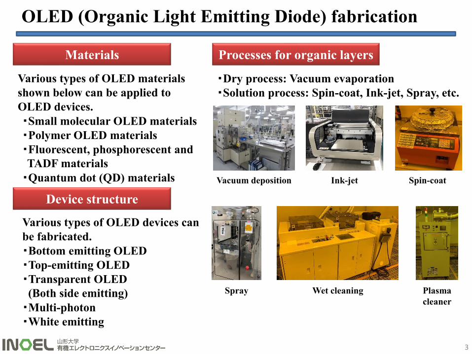
OLED (Organic Light Emitting Diode) fabrication
Various types of OLED materials
shown below can be applied to
OLED devices.
・Small molecular OLED materials
・Polymer OLED materials
・Fluorescent, phosphorescent and
TADF materials
・Quantum dot (QD) materials
・Dry process: Vacuum evaporation
・Solution process: Spin-coat, Ink-jet, Spray, etc.
Various types of OLED devices can
be fabricated.
・Bottom emitting OLED
・Top-emitting OLED
・Transparent OLED
(Both side emitting)
・Multi-photon
・White emitting
Vacuum deposition Ink-jet
Materials Processes for organic layers
Device structure
Spray Wet cleaning
Spin-coat
Plasma
cleaner

4
OPV (Organic Photovoltaic) fabrication
Various types of OPV materials
shown below can be applied to
OPV devices.
・Vacuum deposition materials
・Solution materials
・Quantum dot (QD) materials
Two types of OPV devices can be
fabricated.
・Normal structure
・Inverted structure
Materials Processes for organic layers
Device structure
・Dry process: Vacuum evaporation
・Solution process: Spin-coat, Ink-jet, Spray, etc.
Vacuum deposition Ink-jet
Spray Wet cleaning
Spin-coat
Plasma
cleaner
5
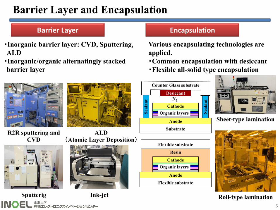
Barrier Layer and Encapsulation
・Inorganic barrier layer: CVD, Sputtering,
ALD
・Inorganic/organic alternatingly stacked
barrier layer
Various encapsulating technologies are
applied.
・Common encapsulation with desiccant
・Flexible all-solid type encapsulation
Barrier Layer Encapsulation
ALD
(Atomic Layer Deposition)
Ink-jet
R2R sputtering and
CVDS
eala
nt
Sea
lan
t
Substrate
Anode
Cathode
Organic layers
Counter Glass substrate
Desiccant
N2
Resin
Flexible substrate
Anode
Cathode
Organic layers
Flexible substrate
Sheet-type lamination
Roll-type laminationSputterig
6
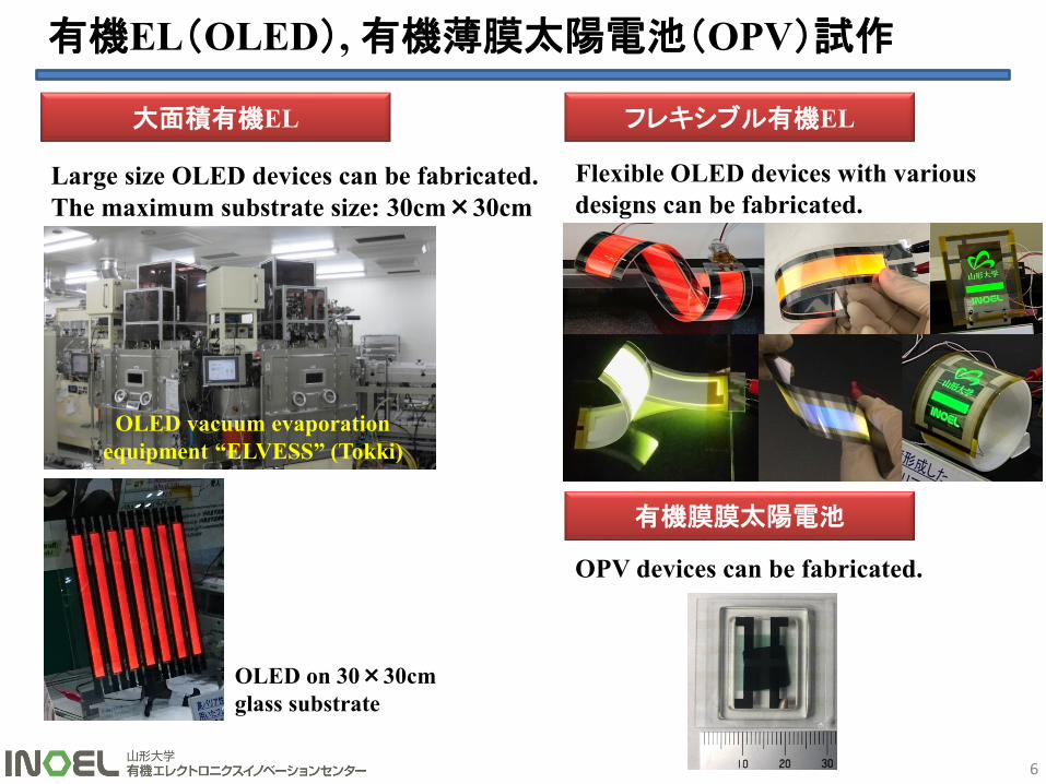
有機EL(OLED), 有機薄膜太陽電池(OPV)試作
OPV devices can be fabricated.
大面積有機EL フレキシブル有機EL
有機膜膜太陽電池
Large size OLED devices can be fabricated.
The maximum substrate size: 30cm×30cm
Flexible OLED devices with various
designs can be fabricated.
OLED vacuum evaporation
equipment “ELVESS” (Tokki)
OLED on 30×30cm
glass substrate
7
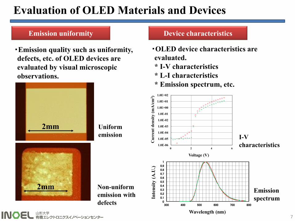
Evaluation of OLED Materials and Devices
Emission uniformity Device characteristics
・Emission quality such as uniformity,
defects, etc. of OLED devices are
evaluated by visual microscopic
observations.
・OLED device characteristics are
evaluated.
* I-V characteristics
* L-I characteristics
* Emission spectrum, etc.
I-V
characteristics
Uniform
emission
Non-uniform
emission with
defects
1.0E-06
1.0E-05
1.0E-04
1.0E-03
1.0E-02
1.0E-01
1.0E+00
1.0E+01
1.0E+02
0 2 4 6
Cu
rren
td
ensi
ty(m
A/c
m2)
1.0E-01
1.0E+00
1.0E+01
1.0E+02
1.0E+03
1.0E+04
1.0E-03 1.0E-02 1.0E-01 1.0E+00 1.0E+01 1.0E+02
Lu
min
an
ce(c
d/m
2)
Current density (mA/cm2)Voltage (V)
0
0.1
0.2
0.3
0.4
0.5
0.6
0.7
0.8
0.9
1
300 400 500 600 700 800
Wavelength (nm)
Inte
nsi
ty (
A.U
.)
Emission
spectrum
8
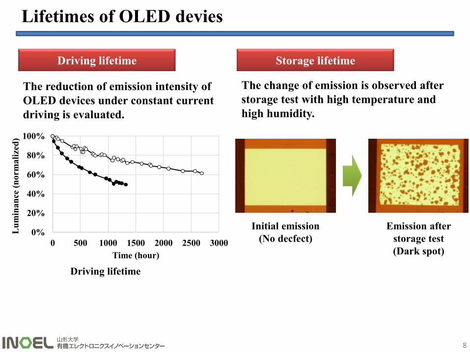
Lifetimes of OLED devies
Driving lifetime Storage lifetime
The reduction of emission intensity of
OLED devices under constant current
driving is evaluated.
The change of emission is observed after
storage test with high temperature and
high humidity.
0%
20%
40%
60%
80%
100%
0 500 1000 1500 2000 2500 3000
Lu
min
an
ce (
no
rma
lize
d)
Time (hour)
Initial emission
(No decfect)
Emission after
storage test
(Dark spot)
Driving lifetime

9
Evaluation of OPV
Equipment
OPV characteristics
Solar simulator
Newport MODEL 66902
1SUN(1000W/m2)
AM1.5 room temp.
About 100,000 LUX
OPV device
10
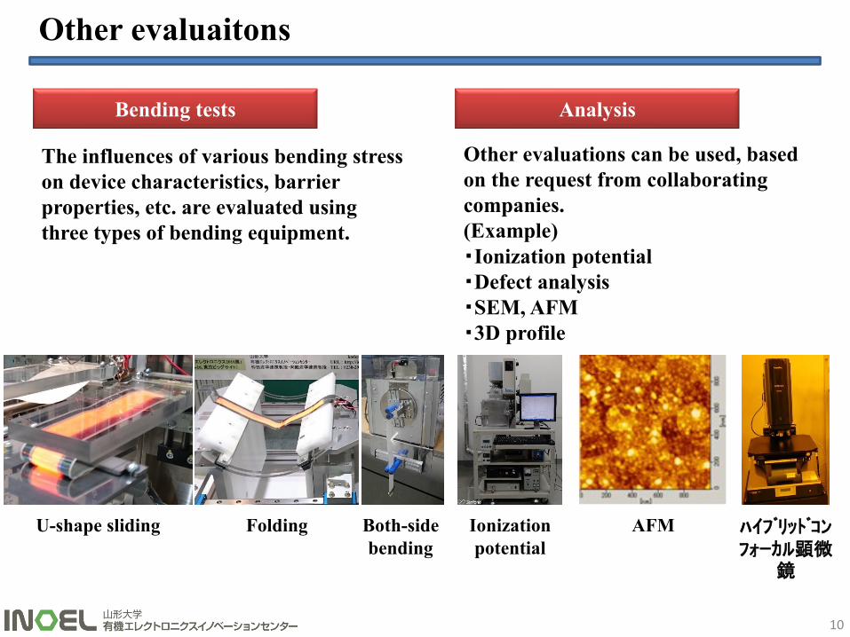
Other evaluaitons
Bending tests Analysis
The influences of various bending stress
on device characteristics, barrier
properties, etc. are evaluated using
three types of bending equipment.
Other evaluations can be used, based
on the request from collaborating
companies.
(Example)
・Ionization potential
・Defect analysis
・SEM, AFM
・3D profile
U-shape sliding Folding Both-side
bending
AFM ハイブリッドコンフォーカル顕微
鏡
Ionization
potential
11
Fabricated flexible organic electronics
devices (OLED and OPV)
Fabricated flexible organic electronics
devices (OLED and OPV)
12
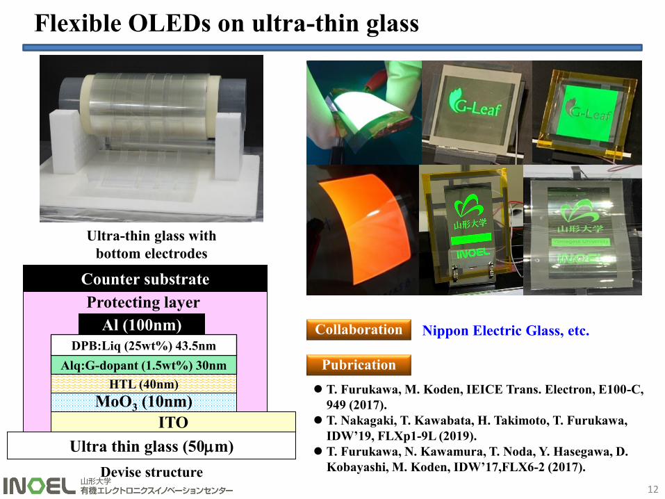
Flexible OLEDs on ultra-thin glass
Protecting layer
ITO
MoO3 (10nm)
Al (100nm)
Ultra thin glass (50mm)
Counter substrate
HTL (40nm)
Alq:G-dopant (1.5wt%) 30nm
DPB:Liq (25wt%) 43.5nm
Ultra-thin glass with
bottom electrodes
Devise structure
Nippon Electric Glass, etc.Collaboration
⚫ T. Furukawa, M. Koden, IEICE Trans. Electron, E100-C,
949 (2017).
⚫ T. Nakagaki, T. Kawabata, H. Takimoto, T. Furukawa,
IDW’19, FLXp1-9L (2019).
⚫ T. Furukawa, N. Kawamura, T. Noda, Y. Hasegawa, D.
Kobayashi, M. Koden, IDW’17,FLX6-2 (2017).
Pubrication

Flexible OLEDs on stainless steel foil
13
Barrier resin
Stainless steel foil (50mm)
Flexible substrate
Semi-transparent cathode
Organic layers
(plural layers)
ITO
Planarization layer (3mm)
Ag alloyStainless steel foil of NIPPON
STEEL CORPORATION GROUP
NIPPON STEEL CORPORATION
NIPPON STEEL Chemical & Material Co., Ltd.Collaroration
⚫ Y. Hagiwara, T. Furukawa, T. Yuki, S. Yamaguchi, N. Yamada, J. Nakatsuka, M. Koden,
H. Nakada, IDW’17, FLXp1-9L (2017).
⚫ M. Koden, T. Furukawa, T. Yuki, H. Kobayashi, H. Nakada, IDW/AD’16, FLX3-1 (2016).
Publication

Flexible OLEDs on barrier film
AEF barrier resin
Organic layers(plural layers)
Cathode
PEN film
IZO
Ag
Barrier layer
Flexible film
Barrier layer
PEN film (50mm)
Insulator(with particles)
Barrier layer
AEF barrier resin
Organic layers(plural layers)
Cathode
Barrier layer
Flexible film
IZO
14
TEIJIN LIMITED, etc.
⚫ K. Taira, Taiga Suzuki, W. Konno, H Chiba, H. Itoh, M. Koden, T. Takahashi, T.
Furukawa, IDW’18, FLX2-4L (2018).
Collaroration
Publication

Concept samples using flexible OLED device
15
KOMORI Corporation / TAKEDA PRINTING CO., LTD.
⚫ Yamagata University; “JFlex2020” (Jan. 2020 / Tokyo).
Flexible substrate
Adhesive resin
Organic layers
(plural layers)
Cathode
TCO (Transparent Conducting Oxide)
Barrier layer
Flexible substrate
Collaroration
Publication

Flexible OLEDs on EXPEEK® barrier film
16
Device size: 50 × 50mm
Emission area: 32 × 32mm
KURABO INDUSTRIES LTD.
⚫ T. Yuki, T. Nishikawa, M. Sugimoto, H. Nakada, M. Koden, IDW’20, FLX2-3 (2020).
⚫ Yamagata University; “JFlex2020” (Jan. 2020 / Tokyo); “JFlex2019” (Jan. 2019 / Tokyo).
⚫ KURABO; “7th Fine Plastic Exhibition” (Dec. 2018 / Tokyo), “SEMICON Japan 2018” (Dec. 2018 / Tokyo).
Collaroration
Publication

Flexible OLEDs with TFEL
17
TOYO INK SC HOLDINGS CO., LTD.
⚫ Yamagata University; “JFlex2020” (Jan. 2020 / Tokyo); “JFlex2019” (Jan. 2019 / Tokyo).
Collaroration
Publication

18
Flexible OLEDs with laminating encapsulation
AEF barrier resin
Organic layers
(plural layers)
Cathode
Flexible substrate
Transparent electrode
Flexible substrate
Exhibited in “Printable Electronics
2018” exhibition (Feb. 2018, Tokyo)
Ajinomoto Co., Inc. /
Ajinomoto Fine-Techno Co., Inc.
Collaroration
Publication
⚫ Yamagata University;“JFlex2019” (Jan. 2019 / Tokyo).

19
Flexible OLED with transparent electrode of Ag nanowire and conducting polymer
Panel size: 50mm x 50mmEmission area: 32mm x 32mm
[*1] Supplied from Ajinomoto Fine-Techno
[*2] developed by Nippon Electric Glass
[*3] developed by Mitsubishi Plastics
Encapsulating layer [*1]
Ultra-thin glass (50mm) [*2]
Conducting polymer
Organic layers
Cathode
Metal foil [*1]
AgNW
Protecting film [*3]
Flexible OLED without ITO was successfully fabricated.
⚫ M. Koden, T. Furukawa, T. Yuki, H. Kobayashi, H. Nakada, IDW/AD’16, FLX3-1 (2016). Publication

Flexible OLEDs with printing non-ITO electrode
Flexible OLED without ITO was successfully fabricated.✓Substrate size : 50mm X 50mm✓Emission aria : 32mm X 32mm
Collaboration by:
✓Yamagata University
✓Dai Nippon Printing
✓DIC
✓Komori Machinery
✓SERIA
✓Taiyo Kikai
20
Encapsulating layer [*]
Organic layers
Ultra-thin glass (50mm)
Cathode
Metal foil [*]
Ag Transparent conducting polymer Insulator
Screen printingScreen
printingFlexography
printingFlexography
printingGravure off-set
printingGravure off-set
printing
[*] supplied from Ajinomoto
Fine-Techno
T. Furukawa, N. Kawamura, M. Sakakibara, M. Koden, International Display
Manufacturing Conference (IDMC’15), S4-4 (2015).

21
substrate:60mm×100mm
Al (Cathode)
Organic layers(plural layers)
PEDOT:PSS
Resin
Substrate (Glass or film)
Cu mesh
Substrate: Glass Substrate: PEN
OLEDs with metal-mesh electrode
Toyo Aluminium K.K., Prof. Takeshi Sano (INOEL, Yamagata University)Collaboration
Publication ⚫ M. Koden, N. Kawamura, T. Yuki, H. Nakada, R. Waguri, K. Den, R. Nakao, H. Minamiyama,
The 31th Meeting of Japan OLED Forum, S7-2 (2020).
⚫ R. Waguri, K. Den, R. Nakao, H. Minamiyama, MES2020, 1B1-2 (2020).
⚫ Yamagata University; “JFlex2020” (Jan. 2020 / Tokyo), “TCTJAPAN” (Jan. 2020 / Tokyo,
“JFlex2019” (Jan. 2019 / Tokyo).

OLEDs with on-demand patterns
2222
⚫ M. Sugimoto, Y. Fukuchi, H. Tsuruta, M.Koden, H. Nakada, T. Yuki, A-COE 2021, PA-17 (2021).
TOYO INK SC HOLDINGS CO., LTD.Collaboration
Publication

Printed flexible OPV fabricated roll-to-roll (R2R) processes
23
MORESCO Corporation / ideal star inc.Collaboration
⚫Yamagata University; “JFlex2020” (Jan. 2020 / Tokyo).
⚫Yamagata University; “PVEXPO 2021”」(Mar. 2021 / Tokyo).
⚫Yamagata University; Press Release 2019.11.6.
⚫MORESCO; Press Release 2019.11.6.
Publication
Features of flexible OPV
Developed technologies
◼Fabricated by roll-to-roll (R2R) printing◼Width:30cm、Length>1m◼Fabrication processes
1) Transparent electrode (TCO) deposition
2) TCO patterning3) Cleaning of substrate4) Printing of ETL(R2R)5) Printing of active layer(R2R)6) Printing of HTL(R2R)7) Printing of electrode(R2R)8) Current collection9) Encapsulation
◼can be applied to windows etc. due to the transparent feature.
◼thin, light weight and un-breakable due to flexible and film
◼applied to various places such as windows, walls, etc. by double-sided tape etc.
Structure of flexible
R2Rprinting

24
Our technologies on flexible organic electronics devices (OLED,
OPV, etc.) contribute practical R&D in industrial companies by
collaborations using our rich knowledge and skills.
Please do not hesitate to contact with us.
Research Group for Flexible Technologies
(Nakada/Furukawa/Yuki/Koden Group)
Innovation Center for Organic Electronics (INOEL)
Yamagata University
URL:https://inoel.yz.yamagata-u.ac.jp/F-consortium/home-e.html
(Contact)
E-mail: [email protected]
E-mail: [email protected]
Summary