carbon nanotube array sensor for mems lab-on-a-chip · lab-on-a-chip devices have the potential to...
TRANSCRIPT

Carbon Nanotube Array Sensor for MEMS Lab-on-a-chip L. Joseph *, V. Veedu ** and D. Garmire ***
*Oceanit, 828 Fort Street Mall, Honolulu Hi, USA, [email protected]
** Oceanit, 828 Fort Street Mall, Honolulu Hi, USA, [email protected]
***University of Hawaii, Honolulu, Hi, USA, [email protected]
ABSTRACT This paper describes fabrication and testing of vertically
aligned carbon nanotube arrays (VANTAs) for biological sensor applications. This structure is created using a standard MEMS process and chemical vapor deposition (CVD) nanotube (NT) post-processing. With further development, the device will be well suited for integration into a microfluidic lab-on-a-chip solution. Included is a spectroscopic characterization of the galvanostatic impedance of the device, as well as scanning electron microscopy (SEM) images. Optical interferometric 3D profiling and X-ray spectroscopy were also used in the characterization. The devices exhibit low resistance, conducting primarily through end regions of the nanotubes where functionalization occurs. The tests validate that this approach is an ideal candidate for low-cost, high-throughput manufacturing of sensitive biochemical sensors.
Keywords: carbon nanotube arrays, biochemical sensor, lab-on-a-chip
1 INTRODUCTION Lab-on-a-chip devices have the potential to provide
point-of-care diagnostics that can save many thousands of lives per year. Adverse drug reactions account for 100,000 deaths annually [1]. One of the primary limitations to wide-spread adoption of lab-on-a-chip technology is the excessive cost of fabrication and integration in high-volume production of these systems. In this paper, we describe a relatively inexpensive, high-volume technique of fabricating well defined patterns of vertically aligned carbon nanotube arrays (VANTAs) using a standard MEMS process, PolyMUMPs, and a single chemical vapor deposition (CVD) step for nanotube growth. VANTA sensor test structures have been fabricated showing vertical growth of over 300 microns, minimum wall width under 20 microns, and high conformance to the defined pattern. In the near future these VANTA sensors will be integrated into a single-die lab-on-a-chip device that includes microfluidics.
Carbon nanotube based devices have been shown to be extremely sensitive biological sensors [2,3,4]; however, these devices require complicated fabrication or post-processing techniques, not compatible with existing high-volume processes. We have developed a simplified method
using standard MEMS process parameters and geometry to create well-defined VANTA sensor structures that can be spaced within close proximity and well suited for sensor geometries. The post-processing steps are fast, low-cost, and uncomplicated. The techniques can be used to create a number of other structures for various applications that use combinations of MEMS and NTs.
2 EXPERIMENTAL SETUP Unlike many published NT biosensors the structure
presented is fabricated using a standard and widely available commercial MEMS process. The MEMSCAP PolyMUMPs process is ideal for the further integration and transition into a production lab-on-a-chip. The PolyMUMPs process consists of three polysilicon layers, two oxide layers and one metal layer. When post-processed using a NT CVD process, this combination provides the capability to create well defined VANTA structures with connectivity to metal contacts. In addition it provides the capability to fabricate on-chip polysilicon microfluidic channels [5] on the same die and system.
Multiple MEMS structures were designed and fabricated on this die as sub components in the development of a lab-on-a-chip sensor. These devices included combinations of sensor structures and microfluidics channels. In addition several other sensor test structures where fabricated. The PolyMUMPs die of all of the lab-on-a-chip subcomponents can be see in Figure 1.
µ-fluidics channel
Figure 1: Multiple sensor and microfluidic channel lab-on-a-chip subsystems fabricated in PolyMUMPs
CNT Growth area
Gold test pads for electrical contact
NSTI-Nanotech 2009, www.nsti.org, ISBN 978-1-4398-1783-4 Vol. 2, 2009 193

2.1 Fabrication and Composition
The VANTA structures fabricated were formed between the pyrolyzed photoresist film (PPF) and the gold contacts, where mismatched thermal expansion coefficients created surface shearing of the PPF. At the interface of the shearing, underlying oxide layers were exposed providing a catalyst site for the growth of multiwalled carbon nanotubes (MWCNT). The thermal shearing occurred in the initial stages of the CNT CVD growth process. Subsequent fabrication of the devices over different time periods showed shearing occurred within the first 5 minutes of exposure in the CVD process. In Figure 2 a Wyko optical interferometric 3D profile is show. This image exhibits the fissure and the early stages of NT growth along the edges of the fissure’s periphery.
Figure 2: Wyko optical interferometric 3D profile of fissure
The CVD process employed was a chemical mixture of a catalyst precursor (ferrocene) and carbon source (xylene) that were atomized and sprayed into a furnace with temperature ranging from 700ºC to 900ºC. Pyrolysis of organic compound deposits carbon nanotubes onto the substrate at the sites of exposed oxide in shear fissures. In future efforts, this process can be simplified by patterning the photoresist to create desired VANTA structures. In Figure 3, a scanning electron micrograph (SEM) of two VANTA structures fabricated using the aforementioned process are shown. The structures shown in Figure 3 are typical of those on the die, exhibiting VANTA of approximately 500µm in height and 500µm across. The structure consists of two VANTA on each side of the fissure that is approximately 20um across. As the VANTA’s height increases, the incidence of physical contact between the VANTA likewise increases. In the biological sensor application the physical and electrical contact is further enhanced when treatment causes the normally hydrophobic NTs to be hydrophilic. When in contact with the test solution the VANTA will be drawn in together increasing physical and electrical contact.
Figure 3: SEM of two VANTA structures fabricated by post processing a PolyMUMPs MEMS die
The process is well suited for biosensor applications for a number of reasons. The most elementary reason is the ability to easily create VANTA structures that are electrically connected to gold contacts. A specific benefit is that the structure forms an electrical test path resulting from the growth of two separate VANTA ribbons on opposite sides of a fissure. In addition another positive characteristic is that the majority of the contact between the two VANTAs is at the top of the structures where the concentration of NT tips is the highest. This can effectively promote the detection current through the tips of the NT where they are most easily carboxalized, which is required for functionalization with antibodies.
The height of the VANTA scales well over time and is controllable to a height of approximately 500µm, provided the CVD process parameters are maintained. Devices ranging from 50µm to 500µm were fabricated all exhibiting similar structural characteristics. The interface between the gold contact and NTs has good electrical continuity, providing a direct electrical interface with the VANTA. In addition to the interface between the gold contact and the VANTA the pyrolyzed photoresist adds an alternate path of conduction from the contact to the VANTA. In this design, the PPF feature is not fully utilized and further investigation of the PPF in the future, will likely yield additional uses. At this time it is unknown how significant the PPF’s contribution is to the connection.
It is desired that the two gold test contacts be electrically connected only through tip to tip VANTA contact. In these prototypes, a conduction pathway across the VANTA junction exists through the fissure. Since the two VANTA are physically separated at the base and touch at the tips the test path can still be characterized. A dilemma is present in determining the cause of the conduction path across the fissure of the gold contacts, from which the VANTA grow. Three conductive paths exist, with the VANTA, PPF, and residual gold all with similar characteristics. Since the gold’s resistivity is 2.4 e -8 Ω・m,
Surface capillary effects will allow biological fluid to
flow to functionalized
VANTAs.
Good electrical conductivity
exists between the gold pads
and the VANTA walls.
VANTA walls grow in parallel vertically
from both sides of the defined fissure.
Gold padCapillary structures
Fissure
Oxide+PPF
1µm
50µm
50µm
NSTI-Nanotech 2009, www.nsti.org, ISBN 978-1-4398-1783-4 Vol. 2, 2009194

the PPF resistivity has been measured as about 1 e -5 Ω・m (about that of graphite) and the VANTA resistivity has been measured approximately as 3 e -5 Ω・m (in the direction along the length of the tubes). It is difficult to determine the absolute conduction path across a fissure from one contact to the other. X-ray spectroscopy has shown that gold is still present in the fissure and it is believed that gold provides a lower path of resistance than through the VANTA. In Figure 4, the X-ray spectroscopy measurement of the inside of the fissure is shown.
Figure 4: X-ray spectroscopy measurement detecting significant amounts of gold in the fissure.
In future devices, better process procedures will provide complete isolation. In this series of preliminary device characterization, the sensor aspect of the VANTA conduction is isolated by using the probe tips rather than the contacts. Although not completely isolated between pads, the continuity between VANTA and its underling contact is independently valuable in the context of future devices.
3 RESULTS
A device was characterized to provide preliminary electrical characterization, prior to biological functionalization. This characterization provides a baseline of the device characteristics and determines continuity between the various contacts and VANTA. In order to account for contact resistance, all characterizations were made using a PARSTAT 2378 potentiostat configured for a 4 wire galvanostatic electronic impedance spectroscopy measurement technique. Our preliminary characterization of functionalized macro-scale VANTA showed that sensitivity to various antigens was acceptable at low frequencies and DC. It is our intent to create a device that provides the necessary sensitivity, but does not require more complicated detection techniques, such as cyclic voltammetry. Future testing will be expanded based on the results of the biological testing. In this series of characterization, the frequency response of the devices were tested from 1 Hz to 2 MHz. It is assumed that 1 Hz closely approximates DC behavior.
Measurements were taken using a Cascade M150 probe station configured with four micromanipulators outfitted
with electrical probes. The probes were connected to the PARSTAT galvanostat and set to measure impedance in a four wire configuration. The four probes were placed across the tops of the VANTA as shown in Figure 5 to directly characterize the impedance through the VANTA structures.
I
V
C.E. W.E.
R.E. S.E.
Carbon Silicon
Gold
Oxygen
Figure 5: Schematic showing device and connectivity used in characterization of VANTA
keV
In this configuration, the contribution from the probe impedance is removed and the impedance between the voltage sensing inner probes is more accurately measured. This impedance is shown over frequency from 1 Hz to 2 MHz in Figure 6. The blue trace is the impedance and the green trace is the phase.
Figure 6: Bode Plot of device impedance from 1 Hz to 2
MHz
Figure 6 shows that the impedance remains close to 13 Ω at low frequencies and begins to increase as reactive components begin contributing around 500 kHz. This increase in reactance continues, until it peaks around 1 MHz, where it then declines back down to close to 15 ohms. The relatively low impedance prior to 500 kHz is well suited for low frequency sensor applications where a low RBefore will likely result in higher sensitivity.
NSTI-Nanotech 2009, www.nsti.org, ISBN 978-1-4398-1783-4 Vol. 2, 2009 195
4 CONCLUSIONS Sensitivity in biosensors is often quantified as shown in Equation 1. Carbon nanotubes are an excellent material for sensor
applications primarily due to their high conductivity and ability to be biologically functionalized. A NT CVD process that is compatible with an existing MEMS fabrication process (PolyMUMPs) has been shown. This process may lead to a cost-effective and simple manufacturing technique for NT biosensors. The device described is an excellent candidate for further refinement and integration into a lab-on-a-chip sensor platform. Continuity between gold contacts and the VANTA was shown, as well as the impedance properties of the array. By optimizing the device dimensions, the path of the test current can be isolated to primarily occur through the tips of the two VANTA. Since the path of current has both transverse and lateral components, electron transport through the VANTA may be particularly sensitive to events such as the charge transfer between antibodies and antigen. Furthermore, the devices low RBefore provides a good baseline resistance for low frequency sensor use, and higher frequency impedance values are also suitable for higher frequency sensor operation. The device was fabricated using a readily available MEMS process and one-step post-processing for growth of the VANTA sensor arrays.
ySensitivitRR
Before
After = (1)
To establish the electrical continuity between the
VANTA and the gold contact a 4 point measurement was taken from the contact to the top of the VANTA structure. Figure 7 shows a schematic of the connection.
I
I
V
W.E.
R.E.
C.E.
S.E.
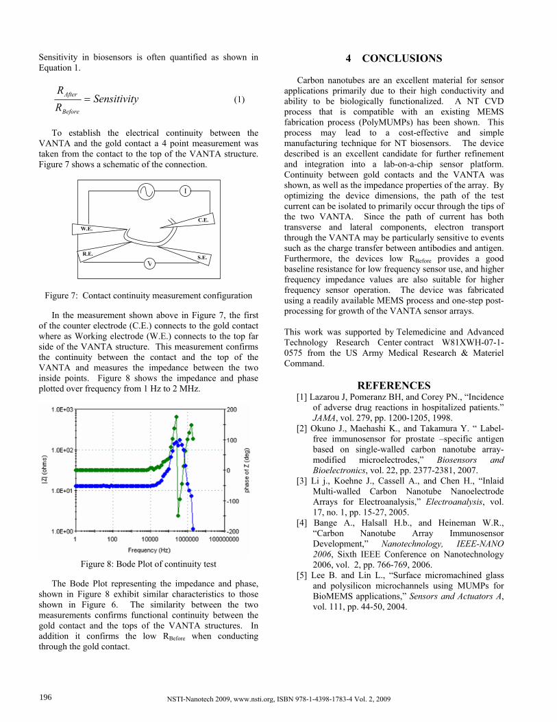
Figure 7: Contact continuity measurement configuration
In the measurement shown above in Figure 7, the first of the counter electrode (C.E.) connects to the gold contact where as Working electrode (W.E.) connects to the top far side of the VANTA structure. This measurement confirms the continuity between the contact and the top of the VANTA and measures the impedance between the two inside points. Figure 8 shows the impedance and phase plotted over frequency from 1 Hz to 2 MHz.
This work was supported by Telemedicine and Advanced Technology Research Center contract W81XWH-07-1-0575 from the US Army Medical Research & Materiel Command.
REFERENCES
[1] Lazarou J, Pomeranz BH, and Corey PN., “Incidence of adverse drug reactions in hospitalized patients.” JAMA, vol. 279, pp. 1200-1205, 1998.
[2] Okuno J., Maehashi K., and Takamura Y. “ Label-free immunosensor for prostate –specific antigen based on single-walled carbon nanotube array-modified microelectrodes,” Biosensors and Bioelectronics, vol. 22, pp. 2377-2381, 2007.
[3] Li j., Koehne J., Cassell A., and Chen H., “Inlaid Multi-walled Carbon Nanotube Nanoelectrode Arrays for Electroanalysis,” Electroanalysis, vol. 17, no. 1, pp. 15-27, 2005.
[4] Bange A., Halsall H.b., and Heineman W.R., “Carbon Nanotube Array Immunosensor Development,” Nanotechnology, IEEE-NANO 2006, Sixth IEEE Conference on Nanotechnology 2006, vol. 2, pp. 766-769, 2006. Figure 8: Bode Plot of continuity test
[5] Lee B. and Lin L., “Surface micromachined glass and polysilicon microchannels using MUMPs for BioMEMS applications,” Sensors and Actuators A, vol. 111, pp. 44-50, 2004.
The Bode Plot representing the impedance and phase, shown in Figure 8 exhibit similar characteristics to those shown in Figure 6. The similarity between the two measurements confirms functional continuity between the gold contact and the tops of the VANTA structures. In addition it confirms the low RBefore when conducting through the gold contact.
NSTI-Nanotech 2009, www.nsti.org, ISBN 978-1-4398-1783-4 Vol. 2, 2009196