buck-boost converter based voltage source inverter using space … · 2014-10-18 · buck-boost...
TRANSCRIPT

IJSRD - International Journal for Scientific Research & Development| Vol. 2, Issue 06, 2014 | ISSN (online): 2321-0613
All rights reserved by www.ijsrd.com 373
Buck-Boost Converter based Voltage Source Inverter using Space Vector
Pulse Width Amplitude modulation Jeetesh Gupta
1 K.P.Singh
2
2Associate Professor
1,2Department of Electrical Engineering
1,2Madan Mohan Malaviya University of Technology, Gorakhpur, India
Abstract— In this paper, a space vector pulse width
amplitude modulation (SVPWAM) technique has been
developed for a Buck-Boost Converter based voltage/
current source Inverter. The switching loss is reduced by
87%, compared to conventional sinusoidal pulse width
modulation (SPWM) technique for a Voltage source
Inverter, and the switching loss is reduced by 60% for
Current source Inverter. The power density is increased by a
factor of 2 to 3 in both cases. In addition it is also proved
that the output harmonics distortion of SVPWAM is lower
than SPWM, by using one third switching frequency of the
latter one. The maximum overall system efficiency 96.7%
has been achieved at full power rating .As a result ,it is
economical to use SVPWAM to make the Buck-Boost
converter based Inverter suitable for application that require
high efficiency, high power density ,high temperature ,and
low cost.
Key words: Buck-Boost converter, SVPWAM, switching
loss reduction, THD
I. INTRODUCTION
Recently, two existing inverter topologies are used for
hybrid electric vehicles (HEVs) and electric vehicles (EVs):
the conventional three-phase inverter with a high voltage
battery and a three-phase pulse width modulation (PWM)
inverter with a dc/dc boost front end. The conventional
PWM inverter imposes high stress on switching devices and
motor thus limits the motor’s constant power speed range
(CPSR), which can be alleviated through the dc–dc boosted
PWM inverter.
The inverter is required to inject low harmonic
current to the motor, in order to reduce the winding loss and
core loss. For this purpose, the switching frequency of the
inverter is designed within a high range from 15 to 20 kHz,
resulting in the switching loss increase in switching device
and also the core loss increase in the motor stator. To solve
this problem, various soft-switching methods have been
proposed [1]–[3]. Active switching rectifier or a diode
rectifier with small DC link capacitor has been proposed in
[4], [5], [8]–[12]. Varies types of modulation method have
been proposed previously such as optimized pulse-width-
modulation [13], improved Space-Vector-PWM control for
different optimization targets and applications [14], and
discontinuous PWM (DPWM). Different switching
sequence arrangement can also affect
The harmonics, power loss and voltage/current
ripples .DPWM has been widely used to reduce the
switching frequency, by selecting only one zero vector in
one sector. It results in 50% switching frequency reduction.
However, if an equal output THD is required, DPWM
cannot reduce switching loss than SPWM.
In this paper, a space vector pulse width amplitude
modulation (SVPWAM) technique has been developed for a
Buck-Boost Converter based voltage/ current source
Inverter. By eliminating conventional zero vector in Space
Vector Modulation, one third and two third switching
frequency reduction in CSI and VSI can be achieved,
respectively. An 87% switching loss reduction can be
achieved in VSI, and a 74% reduction can be achieved in
CSI when unity power factor is assumed. Therefore, a high-
efficiency, high-power density, high-temperature, and low
cost 1-kW inverter is achieved by using an SVPWAM
method.
Fig. 1: SVPWAM for
Fig. 2: DC Link Voltage for SVPWAM in VSI
II. SVPWAM FOR VSI
A. Principle of SVPWAM control technique in VSI
The principle of an SVPWAM control technique is to
eliminate the zero vector in each sector. The modulation
principle of SVPWAM is shown in Fig. 1. In each sector,
only one phase leg is doing PWM switching; thus, the
switching frequency is reduced by two-third. This imposes
zero switching for one phase leg in the adjacent two sectors.
For example, in sector VI and I, phase leg A has no

Buck-Boost Converter based Voltage Source Inverter using Space Vector Pulse Width Amplitude modulation
(IJSRD/Vol. 2/Issue 06/2014/082)
All rights reserved by www.ijsrd.com 374
switching at all. The dc-link voltage thus is directly
generated from the output line-to-line voltage. In sector I, no
zero vector is selected. Therefore, S1 and S2 keep constant
ON, and S3 and S6 are doing PWM switching. As a result, if
the output voltage is kept at the normal three-phase
sinusoidal voltage, the dc-link voltage should be equal to
line-to-line voltage Vac at this time. Consequently, the dc-
link voltage should present a 6ω varied feature to maintain a
desired output voltage. The corresponding waveform is
shown in Fig. 2. A dc–dc conversion is needed in the front
stage to generate this 6ω voltage.
The original equations for time period are
√
√
(1)
Fig. 3: Vector placement in each sector
Where θ ∈ [0, π/3] is relative angle from the output
voltage vector to the first adjacent basic voltage vector like
in Fig 1. If the time period for each vector maintains the
same, the switching frequency will vary with angle, which
results in a variable inductor current ripple and muti
frequency output harmonics. Therefore, in order to keep the
switching period constant but still keep the same pulse width
as the original one, the new time periods can be calculated
as
(2)
Fig. 4: simulink model of SVPWAM for VSI
Fig. 5: Theoretical waveform of output line to line voltage
Fig. 6: Switching signals SVPWAM for VSI
B. Inverter Switching Loss Reduction for VSI
In VSI, the device voltage stress is equal to dc-link voltage
, and the current stress is equal to output current .
Thus the switching loss for each switch is
[∫
| |
⁄
⁄
∫
| |
⁄
⁄
]
= √
(3)
Where , are the references.
Since the SVPWAM only has PWM switching in
two 60 degrees sections, the integration over 2π can be
narrowed down into integration within two 60 degrees
= √
(4)
The switching loss for a conventional SPWM method is
=
(5)
III. TOPOLOGY OF SVPWAM
The topologies that can utilize SVPWAM have two stages:
dc–dc conversion which converts a dc voltage or current
into a 6ω varied dc-link voltage or current; VSI for which
SVPWAM is applied. One typical example of this structure
is the boost converter inverter discussed previously.
However, the same function can also be implemented in a
single stage. The front stage can also be integrated with
inverter to form a single stage. Example. Instead of controlling the dc-link current
to have a constant average value, the open zero state
duty cycle will be regulated instantaneously to control
to have a 6ω fluctuate average value, resulting in a
pulse type 6ω waveform at the real dc-link current ,
since I1 is related to the input dc current by a transfer
function.

Buck-Boost Converter based Voltage Source Inverter using Space Vector Pulse Width Amplitude modulation
(IJSRD/Vol. 2/Issue 06/2014/082)
All rights reserved by www.ijsrd.com 375
Fig . 7: SVPWAM-based boost-converter-inverter motor
drive system
(6)
IV. 1-KW BOOST-CONVERTER INVERTER FOR EV MOTOR
DRIVE APPLICATION
A. Operating Principle
The circuit schematic and control system for a 1-kW Boost
converter inverter motor drive system is shown in Fig. 7. A
6ω dc-link voltage is generated from a constant dc voltage
by a boost converter, using open-loop control. Inverter then
could be modulated by a SVPWAM method. The
specifications for the system are input voltage is 100–200 V;
the average dc-link voltage is 300 V; output line-to-line
voltage RMS is 230 V; and frequency is from 60 Hz to 1
kHz.
Fig. 8: Simulink model of SVPWAM-based boost-
converter-inverter motor drive system
In SVPWAM control of boost mode, dc-link voltage varies
with the output voltage, in which the modulation index is
always kept maximum. So, when dc-link voltage is above
the battery voltage, dc-link voltage level varies with the
output voltage. The voltage utilization increased and the
total power stress on the devices has been reduced.
B. Variable DC-Link SPWM Control at High Frequency
When the output needs to operate at a relative high
frequency, like between 120 Hz and 1 kHz, it is challenging
to obtain a 6ω dc-link voltage without increasing the
switching frequency of a boost converter. Because the
controller does not have enough bandwidth. Furthermore,
increasing boost converter switching frequency would cause
a substantial increase of the total switching loss, because it
takes up more than 75% of the total switching loss. The
reason is because it switches at a complete current region.
Also a normal SPWM cannot be used in this range because
the capacitor is designed to be small that it cannot hold a
constant dc link voltage. Therefore, the optimum option is to
control the dc link voltage to be 6ω and do a variable dc link
SPWM modulation. In this variable dc-link SPWM control,
in order to get better utilization of the dc-link voltage, an
integer times between the dc-link fundamental frequency
and output frequency is preferred. When the output
frequency is in [60 Hz, 120 Hz], a 6ω dc link is chosen;
when the frequency is in [120 Hz, 240 Hz], a 3ω dc link is
chosen; when the frequency is in [240 Hz, 360 Hz], a 2ω dc
link is chosen.
C. Test Results of Boost converter VSI using SVPWAM
(1) SVPWAM Control at 60 Hz: Figs. 9-12 show the
output and input voltage, current waveform when
input voltage increases from 20 to 100 V, while
keeping the boost ratio constant. In this case, the
output voltage increases linearly with input voltage
increase. The output power increases in proportion
to square of the input voltage. The parameters used
in this test are input voltage 20 V, average dc link
voltage is 60 V, RMS Voltage is 46V,rated power
40W, Switching frequency 20 KHz and output
frequency is 60 Hz.
Fig. 9: DC Link Voltage

Buck-Boost Converter based Voltage Source Inverter using Space Vector Pulse Width Amplitude modulation
(IJSRD/Vol. 2/Issue 06/2014/082)
All rights reserved by www.ijsrd.com 376
Fig. 10: Three phase output voltage before filter
Fig. 11: Three phase output voltage after filter
Fig. 12: Three phase output current before filter
Fig. 13: Three phase output current after filter
(2) A 1-kW boost-converter inverter prototype has
been built in the laboratory to implement the
SVPWAM control at 60 Hz and SPWM control at
1 kHz.in order to demonstrate their merits in
reducing power loss and reducing the size
compared to traditional methods. The Parameters
are use in this test are rated power: 1 kW; battery
voltage: 100–200 V; rated line voltage RMS: 230
V; dc-link voltage peak: 324 V; switching
frequency: 20 kHz; output frequency: 60 Hz–1
KHz .
Fig. 14: DC Link Voltage
Fig. 15: Three phase output voltage before filter
Fig. 16: Three phase output voltage after filter
Fig. 17: Three phase output current before filter
Fig. 18: Three phase output current after filter
V. FFT ANALYSIS FOR BUCK-BOOST CONVERTER VSI USING
SVPWAM
The object of THD analysis is the output voltage or current
before filter. The reason is that certain orders of harmonics
can be eliminated by sum of switching functions in VSI. The
modulation index selected here is the maximum modulation
index 1.15, since the SVPWAM always only has the
maximum modulation index. Theoretically, the THD varies
with modulation index. The dc-link voltage is designed to
be a constant for SVPWM and an ideal 6ω envelope of the
output six line-to-line voltages for SVPWAM. Thus, the
harmonic of the SVPWAM here does not contain the
harmonics from the dc–dc converter output. It is direct
comparison between two modulation methods from
mathematics point of view. We get 4.74 % THD in
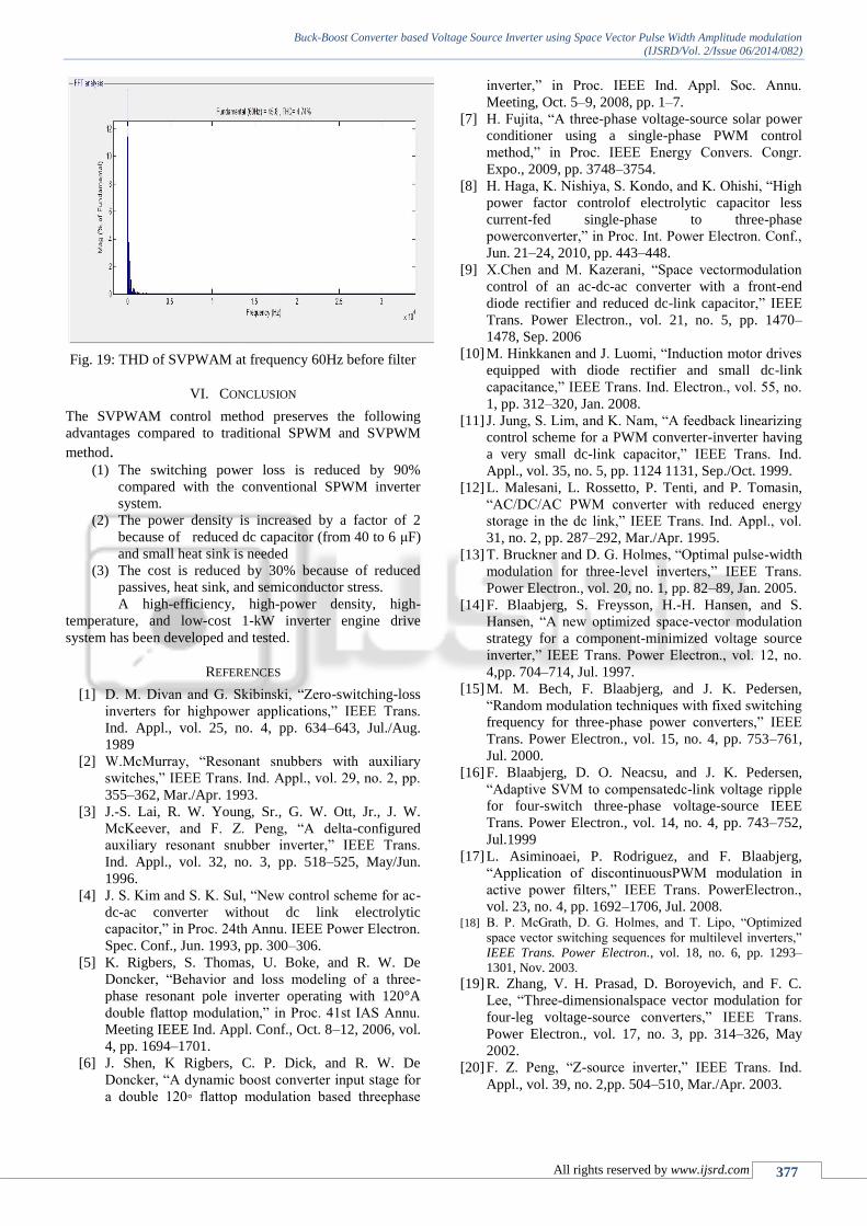
SVPWAM control for Buck boost VSI.
Buck-Boost Converter based Voltage Source Inverter using Space Vector Pulse Width Amplitude modulation
(IJSRD/Vol. 2/Issue 06/2014/082)
All rights reserved by www.ijsrd.com 377
Fig. 19: THD of SVPWAM at frequency 60Hz before filter
VI. CONCLUSION
The SVPWAM control method preserves the following
advantages compared to traditional SPWM and SVPWM
method. (1) The switching power loss is reduced by 90%
compared with the conventional SPWM inverter
system.
(2) The power density is increased by a factor of 2
because of reduced dc capacitor (from 40 to 6 μF)
and small heat sink is needed
(3) The cost is reduced by 30% because of reduced
passives, heat sink, and semiconductor stress.
A high-efficiency, high-power density, high-
temperature, and low-cost 1-kW inverter engine drive
system has been developed and tested.
REFERENCES
[1] D. M. Divan and G. Skibinski, “Zero-switching-loss
inverters for highpower applications,” IEEE Trans.
Ind. Appl., vol. 25, no. 4, pp. 634–643, Jul./Aug.
1989
[2] W.McMurray, “Resonant snubbers with auxiliary
switches,” IEEE Trans. Ind. Appl., vol. 29, no. 2, pp.
355–362, Mar./Apr. 1993.
[3] J.-S. Lai, R. W. Young, Sr., G. W. Ott, Jr., J. W.
McKeever, and F. Z. Peng, “A delta-configured
auxiliary resonant snubber inverter,” IEEE Trans.
Ind. Appl., vol. 32, no. 3, pp. 518–525, May/Jun.
1996.
[4] J. S. Kim and S. K. Sul, “New control scheme for ac-
dc-ac converter without dc link electrolytic
capacitor,” in Proc. 24th Annu. IEEE Power Electron.
Spec. Conf., Jun. 1993, pp. 300–306.
[5] K. Rigbers, S. Thomas, U. Boke, and R. W. De
Doncker, “Behavior and loss modeling of a three-
phase resonant pole inverter operating with 120°A
double flattop modulation,” in Proc. 41st IAS Annu.
Meeting IEEE Ind. Appl. Conf., Oct. 8–12, 2006, vol.
4, pp. 1694–1701.
[6] J. Shen, K Rigbers, C. P. Dick, and R. W. De
Doncker, “A dynamic boost converter input stage for
a double 120◦ flattop modulation based threephase
inverter,” in Proc. IEEE Ind. Appl. Soc. Annu.
Meeting, Oct. 5–9, 2008, pp. 1–7.
[7] H. Fujita, “A three-phase voltage-source solar power
conditioner using a single-phase PWM control
method,” in Proc. IEEE Energy Convers. Congr.
Expo., 2009, pp. 3748–3754.
[8] H. Haga, K. Nishiya, S. Kondo, and K. Ohishi, “High
power factor controlof electrolytic capacitor less
current-fed single-phase to three-phase
powerconverter,” in Proc. Int. Power Electron. Conf.,
Jun. 21–24, 2010, pp. 443–448.
[9] X.Chen and M. Kazerani, “Space vectormodulation
control of an ac-dc-ac converter with a front-end
diode rectifier and reduced dc-link capacitor,” IEEE
Trans. Power Electron., vol. 21, no. 5, pp. 1470–
1478, Sep. 2006
[10] M. Hinkkanen and J. Luomi, “Induction motor drives
equipped with diode rectifier and small dc-link
capacitance,” IEEE Trans. Ind. Electron., vol. 55, no.
1, pp. 312–320, Jan. 2008.
[11] J. Jung, S. Lim, and K. Nam, “A feedback linearizing
control scheme for a PWM converter-inverter having
a very small dc-link capacitor,” IEEE Trans. Ind.
Appl., vol. 35, no. 5, pp. 1124 1131, Sep./Oct. 1999.
[12] L. Malesani, L. Rossetto, P. Tenti, and P. Tomasin,
“AC/DC/AC PWM converter with reduced energy
storage in the dc link,” IEEE Trans. Ind. Appl., vol.
31, no. 2, pp. 287–292, Mar./Apr. 1995.
[13] T. Bruckner and D. G. Holmes, “Optimal pulse-width
modulation for three-level inverters,” IEEE Trans.
Power Electron., vol. 20, no. 1, pp. 82–89, Jan. 2005.
[14] F. Blaabjerg, S. Freysson, H.-H. Hansen, and S.
Hansen, “A new optimized space-vector modulation
strategy for a component-minimized voltage source
inverter,” IEEE Trans. Power Electron., vol. 12, no.
4,pp. 704–714, Jul. 1997.
[15] M. M. Bech, F. Blaabjerg, and J. K. Pedersen,
“Random modulation techniques with fixed switching
frequency for three-phase power converters,” IEEE
Trans. Power Electron., vol. 15, no. 4, pp. 753–761,
Jul. 2000.
[16] F. Blaabjerg, D. O. Neacsu, and J. K. Pedersen,
“Adaptive SVM to compensatedc-link voltage ripple
for four-switch three-phase voltage-source IEEE
Trans. Power Electron., vol. 14, no. 4, pp. 743–752,
Jul.1999
[17] L. Asiminoaei, P. Rodriguez, and F. Blaabjerg,
“Application of discontinuousPWM modulation in
active power filters,” IEEE Trans. PowerElectron.,
vol. 23, no. 4, pp. 1692–1706, Jul. 2008. [18] B. P. McGrath, D. G. Holmes, and T. Lipo, “Optimized
space vector switching sequences for multilevel inverters,”
IEEE Trans. Power Electron., vol. 18, no. 6, pp. 1293–
1301, Nov. 2003.
[19] R. Zhang, V. H. Prasad, D. Boroyevich, and F. C.
Lee, “Three-dimensionalspace vector modulation for
four-leg voltage-source converters,” IEEE Trans.
Power Electron., vol. 17, no. 3, pp. 314–326, May
2002.
[20] F. Z. Peng, “Z-source inverter,” IEEE Trans. Ind.
Appl., vol. 39, no. 2,pp. 504–510, Mar./Apr. 2003.