brochure of mx3700xxa waveform pattern
TRANSCRIPT

MX3700xxA Waveform PatternMX370x series software
MG3700A Vector Signal Generator
Product Brochure
2 Product Brochure l MX3700xxA
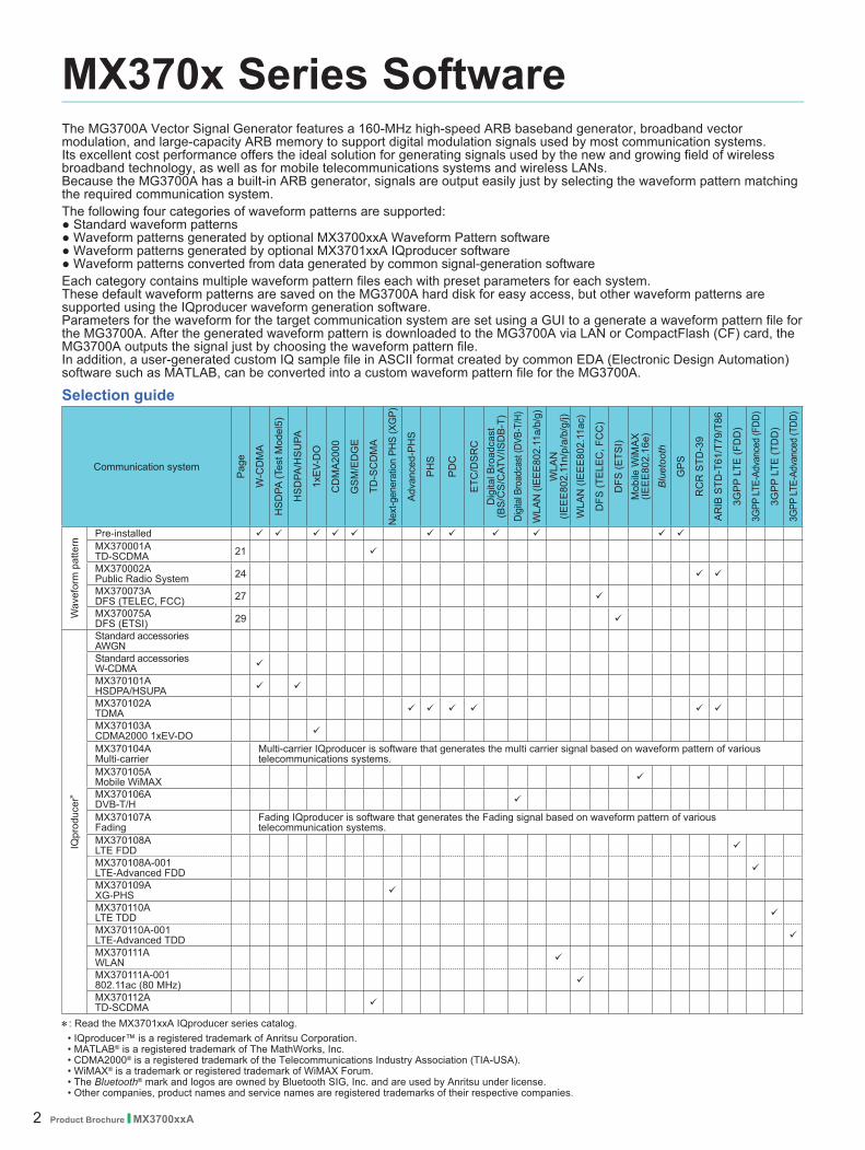
The MG3700A Vector Signal Generator features a 160-MHz high-speed ARB baseband generator, broadband vector modulation, and large-capacity ARB memory to support digital modulation signals used by most communication systems. Its excellent cost performance offers the ideal solution for generating signals used by the new and growing field of wireless broadband technology, as well as for mobile telecommunications systems and wireless LANs.Because the MG3700A has a built-in ARB generator, signals are output easily just by selecting the waveform pattern matching the required communication system.The following four categories of waveform patterns are supported: Standard waveform patterns Waveform patterns generated by optional MX3700xxA Waveform Pattern software Waveform patterns generated by optional MX3701xxA IQproducer software Waveform patterns converted from data generated by common signal-generation softwareEach category contains multiple waveform pattern files each with preset parameters for each system.These default waveform patterns are saved on the MG3700A hard disk for easy access, but other waveform patterns are supported using the IQproducer waveform generation software.Parameters for the waveform for the target communication system are set using a GUI to a generate a waveform pattern file for the MG3700A. After the generated waveform pattern is downloaded to the MG3700A via LAN or CompactFlash (CF) card, the MG3700A outputs the signal just by choosing the waveform pattern file.In addition, a user-generated custom IQ sample file in ASCII format created by common EDA (Electronic Design Automation) software such as MATLAB, can be converted into a custom waveform pattern file for the MG3700A.
Selection guide
Communication system
Pag
e
W-C
DM
A
HS
DPA
(Tes
t Mod
el5)
HS
DPA
/HS
UPA
1xE
V-D
O
CD
MA
2000
GS
M/E
DG
E
TD-S
CD
MA
Nex
t-gen
erat
ion
PHS
(XG
P)
Adv
ance
d-P
HS
PH
S
PD
C
ETC
/DS
RC
Dig
ital B
road
cast
(B
S/C
S/C
ATV
/ISD
B-T
)Di
gital
Broa
dcas
t (DV
B-T/
H)
WLA
N (I
EEE8
02.1
1a/b
/g)
WLA
N
(IEE
E80
2.11
n/p/
a/b/
g/j)
WLA
N (I
EE
E80
2.11
ac)
DFS
(TE
LEC
, FC
C)
DFS
(ETS
I)M
obile
WiM
AX
(IE
EE
802.
16e)
Blu
etoo
th
GP
S
RC
R S
TD-3
9
AR
IB S
TD-T
61/T
79/T
86
3GP
P LT
E (F
DD
)
3GPP
LTE-
Adva
nced
(FDD
)
3GP
P LT
E (T
DD
)
3GPP
LTE-
Adva
nced
(TDD
)
Wav
efor
m p
atte
rn
Pre-installed MX370001A TD-SCDMA 21
MX370002A Public Radio System 24
MX370073A DFS (TELEC, FCC) 27
MX370075A DFS (ETSI) 29
IQpr
oduc
er*
Standard accessories AWGNStandard accessories W-CDMA
MX370101A HSDPA/HSUPA
MX370102A TDMA
MX370103A CDMA2000 1xEV-DO
MX370104A Multi-carrier
Multi-carrier IQproducer is software that generates the multi carrier signal based on waveform pattern of various telecommunications systems.
MX370105A Mobile WiMAX
MX370106A DVB-T/H
MX370107A Fading
Fading IQproducer is software that generates the Fading signal based on waveform pattern of various telecommunication systems.
MX370108A LTE FDD
MX370108A-001 LTE-Advanced FDD
MX370109A XG-PHS
MX370110A LTE TDD
MX370110A-001 LTE-Advanced TDD
MX370111A WLAN
MX370111A-001 802.11ac (80 MHz)
MX370112A TD-SCDMA
*: Read the MX3701xxA IQproducer series catalog. • IQproducer™ is a registered trademark of Anritsu Corporation. • MATLAB® is a registered trademark of The MathWorks, Inc. • CDMA2000® is a registered trademark of the Telecommunications Industry Association (TIA-USA). • WiMAX® is a trademark or registered trademark of WiMAX Forum. • The Bluetooth® mark and logos are owned by Bluetooth SIG, Inc. and are used by Anritsu under license. • Other companies, product names and service names are registered trademarks of their respective companies.
MX370x Series Software

Product Brochure l MX3700xxA 3

4 Product Brochure l MX3700xxA
Additive White Gaussian Noise (AWGN) Waveform Patterns AWGN Waveform PatternsThe AWGN waveform patterns listed in the table below are stored on the MG3700A internal hard disk.Signals for evaluating the UE receiver and transmitter performance and modules, etc., are output by selecting one of these AWGN waveform patterns.
Waveform Pattern Screen
In-band AWGN Power Screen
Standard
Waveform Patterns MAX Peak/ RMS Ratio
3 dB Bandwidth(MHz)
In-band PowerConversion Ratio (dB)* Evaluation
AWGN_3_84MHz_x2 >12 dB 7.68 3.01 Added with W-CDMA UL signal to test dynamic rangeAWGN_3_84MHz_x1_5 >12 dB 5.76 1.76 Added with W-CDMA UL signal to test dynamic range
AWGN_1.23MHz_x2 >12 dB 2.46 3.01 Added with reverse signals of CDMA2000 or CDMA2000 1xEV-DO to test dynamic range
AWGN_1.23MHz_x1_5 >12 dB 3.69 1.76 Added with reverse signals of CDMA2000 or CDMA2000 1xEV-DO to test dynamic range
*: The in-band power conversion ratio is the ratio of the system bandwidth of each communication system to the total power of the MG3700A output measured with a power meter or equivalent device.
Product Brochure l MX3700xxA 5
AWGN Waveform PatternsStandard
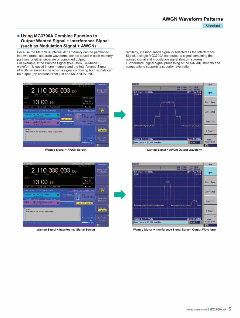
Using MG3700A Combine Function to Output Wanted Signal + Interference Signal (such as Modulation Signal + AWGN)
Because the MG3700A internal ARB memory can be partitioned into two areas, separate waveforms can be saved in each memory partition for either separate or combined output.For example, if the Wanted Signal (W-CDMA, CDMA2000) waveform is saved in one memory and the Interference Signal (AWGN) is saved in the other, a signal combining both signals can be output (top screens) from just one MG3700A unit.
Similarly, if a modulation signal is selected as the Interference Signal, a single MG3700A can output a signal combining the wanted signal and modulation signal (bottom screens).Furthermore, digital signal processing of the S/N adjustments and computations supports a superior level ratio.
Wanted Signal + AWGN Screen
Wanted Signal + Interference Signal Screen
Wanted Signal + AWGN Output Waveform
Wanted Signal + Interference Signal Screen Output Waveform

6 Product Brochure l MX3700xxA
W-CDMA Waveform Patterns W-CDMA Waveform PatternsThe following W-CDMA waveform patterns are installed on the internal hard disk when MG3700A Vector Signal Generator is installed. Details for each pattern file is given on the next page.
• For Evaluating Base Station Transmitter Devices (TS 25.141 Test Model 1 to 4)
TestModel_1_16DPCHTestModel_1_32DPCHTestModel_1_64DPCHTestModel_1_64x2_10MTestModel_1_64x2_15MTestModel_2TestModel_3_16DPCHTestModel_3_32DPCHTestModel_4TestModel_5_2HSPDSCHTestModel_5_4HSPDSCHTestModel_5_8HSPDSCHTestModel_6_8HSPDSCHTestModel_1_64DPCHx2TestModel_1_64DPCHx3TestModel_1_64DPCHx4DL_CPICH
• For Testing BS Receiver Performance (TS 25.101/ 25.104 UL RMC 12.2 to 384 kbps)
UL_RMC_12_2kbpsUL_RMC_12_2kbps_ACSUL_RMC_64kbpsUL_RMC_144kbpsUL_RMC_384kbpsUL_AMR_TFCS1UL_AMR_TFCS2UL_AMR_TFCS3UL_ISDNUL_64kbps_PacketUL_InterfereUL_Interfere_ov3
• For Evaluating UE Transmitter Devices (TS 25.101 A2.1)
UL_RMC_12_2kbps_TX
• For Testing UE Receiver Performance (TS 25.101 DL RMC 12.2 to 384 kbps)
DL_RMC_12_2kbps_RXDL_RMC_12_2kbpsDL_RMC_12_2kbps_MILDL_RMC_12_2kbps_ACSDL_RMC_64kbpsDL_RMC_144kbpsDL_RMC_384kbpsDL_AMR_TFCS1DL_AMR_TFCS2DL_AMR_TFCS3DL_ISDNDL_384kbps_PacketDL_InterfereDL_Interfere_ov3P_CCPCH
Uplink and downlink W-CDMA modulation signals conforming to the 3GPP (FDD) standards can be output simply by selecting the waveform from the patterns on the MG3700A internal hard disk without setting any complex 3GPP-compliant parameters.
Standard
Selecting Waveform Pattern

Product Brochure l MX3700xxA 7
W-CDMA Waveform Patterns
• W-CDMA Waveform Patterns ListWaveform Patterns UL/DL Channel 3GPP (Release1999) Evaluation
UL_RMC_12_2kbps
UL
DPCCH, DPDCHTS 25.141 A.2
BS RX Test
UL_RMC_12_2kbps_ACS*1 DPCCH, DPDCHUL_RMC_64kbps*1 DPCCH, DPDCH TS 25.141 A.3UL_RMC_144kbps*1 DPCCH, DPDCH TS 25.141 A.4UL_RMC_384kbps*1 DPCCH, DPDCH TS 25.141 A.5UL_AMR_TFCS1 DPCCH, DPDCH
TS 25.944 4.1.2UL_AMR_TFCS2 DPCCH, DPDCHUL_AMR_TFCS3 DPCCH, DPDCHUL_ISDN*1 DPCCH, DPDCHUL_64kbps_Packet DPCCH, DPDCHUL_Interfere DPCCH, DPDCH
TS 25.141 IUL_Interfere_ov3 DPCCH, DPDCH
UL_RMC_12_2kbps_TX DPCCH, DPDCH TS 25.101 A.2.1 UE TX Device Test
P_CCPCH*2
DL
P-CCPCH TS 25.944 4.1.1*3
UE RX Test
DL_RMC_12_2kbps_RX*2 P-CPICH, SCH, PICH, DPCHTS 25.101 A.3.1TS 25.101 C.3.1DL_RMC_12_2kbps_ACS*1 P-CPICH, SCH, PICH, DPCH, P-CCPCH
DL_RMC_12_2kbps_MIL*2 P-CPICH, SCH, PICH, DPCH, OCNSDL_RMC_12_2kbps*2 P-CPICH, SCH, PICH, DPCH, OCNS TS 25.101 A.3.1/C3.2DL_RMC_64kbps*2 P-CPICH, SCH, PICH, DPCH, OCNS TS 25.101 A.3.2/C3.2DL_RMC_144kbps*2 P-CPICH, SCH, PICH, DPCH, OCNS TS 25.101 A.3.3/C3.2DL_RMC_384kbps*2 P-CPICH, SCH, PICH, DPCH, OCNS TS 25.101 A.3.4/C3.2DL_AMR_TFCS1*2 P-CPICH, SCH, PICH, DPCH, OCNS
TS 25.944 4.1.1.3TS 25.101 C.3.2
DL_AMR_TFCS2*2 P-CPICH, SCH, PICH, DPCH, OCNSDL_AMR_TFCS3*2 P-CPICH, SCH, PICH, DPCH, OCNSDL_ISDN*2 P-CPICH, SCH, PICH, DPCH, OCNSDL_384kbps_Packet*2 P-CPICH, SCH, PICH, DPCH, OCNSDL_Interfere P-CPICH, P-CCPCH, SCH, PICH, OCNS
TS 25.101 C.4DL_Interfere_ov3*6 P-CPICH, P-CCPCH, SCH, PICH, OCNSDL_CPICH P-CPICH –
BS TX Device Test
TestModel_1_16DPCH P-CPICH, P-CCPCH, SCH, PICH, S-CCPCH, 16DPCH
TS 25.141 6.1.1
TestModel_1_32DPCH P-CPICH, P-CCPCH, SCH, PICH, S-CCPCH, 32DPCHTestModel_1_64DPCH P-CPICH, P-CCPCH, SCH, PICH, S-CCPCH, 64DPCHTestModel_1_64DPCHx2*4 P-CPICH, P-CCPCH, SCH, PICH, S-CCPCH, 64DPCHTestModel_1_64DPCHx3*4 P-CPICH, P-CCPCH, SCH, PICH, S-CCPCH, 64DPCHTestModel_1_64DPCHx4*4 P-CPICH, P-CCPCH, SCH, PICH, S-CCPCH, 64DPCHTestModel_1_64x2_10M*4, *5 P-CPICH, P-CCPCH, SCH, PICH, S-CCPCH, 64DPCHTestModel_1_64x2_15M*4, *5 P-CPICH, P-CCPCH, SCH, PICH, S-CCPCH, 64DPCHTestModel_2 P-CPICH, P-CCPCH, SCH, PICH, S-CCPCH, 3DPCHTestModel_3_16DPCH P-CPICH, P-CCPCH, SCH, PICH, S-CCPCH, 16DPCHTestModel_3_32DPCH P-CPICH, P-CCPCH, SCH, PICH, S-CCPCH, 32DPCHTestModel_4 P-CCPCH, SCH
TestModel_5_2HSPDSCH P-CPICH, P-CCPCH, SCH, PICH, S-CCPCH, 6DPCH, HS-SCCH, 2HS-PDSCH
TestModel_5_4HSPDSCH P-CPICH, P-CCPCH, SCH, PICH, S-CCPCH, 14DPCH, HS-SCCH, 4HS-PDSCH
TestModel_5_8HSPDSCH P-CPICH, P-CCPCH, SCH, PICH, S-CCPCH, 30DPCH, HS-SCCH, 8HS-PDSCH
TestModel_6_8HSPDSCH P-CPICH, P-CCPCH, SCH, PICH, S-CCPCH, 30DPCH, HS-SCCH, 8HS-PDSCH TS 25.141 8.2.0
*1: The UL_RMC_12_2kbps_ACS, UL_RMC_64kbps, UL_RMC_144kbps, UL_RMC_384kbps, UL_ISDN and DL_RMC_12_2kbps_ACS patterns can be added to the standard AWGN waveform pattern only when the optional ARB Memory Expansion 512 Msamples (Option 021/121) is installed.
*2: Since waveform patterns (excluding DL_RMC12_2kbps_ACS) for the UE RX test do not include P-CCPCH, they must be used in combination with a P-CCPCH waveform pattern.
*3: A 12-bit SFN is added to the head of each BCH Transport block.*4: x2, x3, and x4 indicate multi-carrier 2, 3, and 4, respectively.*5: 10 M and 15 M indicate the multi-carrier inter frequency gap.*6: Select a waveform pattern generated using the W-CDMA waveform pattern generation function of the MG3700A IQproducer or by the MX370101A HSDPA
IQproducer (only the waveform patterns that can be configured using only one memory) for memory A on the MG3700A while selecting this pattern for memory B to output a signal that is generated by adding the desired signal and the interference signal using baseband.
Standard
8 Product Brochure l MX3700xxA
W-CDMA Waveform PatternsStandard
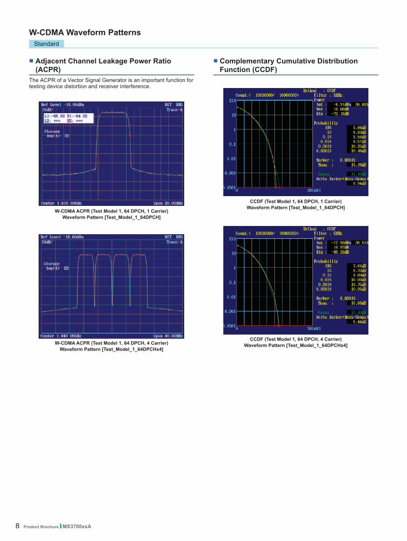
Adjacent Channel Leakage Power Ratio (ACPR)
The ACPR of a Vector Signal Generator is an important function for testing device distortion and receiver interference.
Complementary Cumulative Distribution Function (CCDF)
W-CDMA ACPR (Test Model 1, 64 DPCH, 1 Carrier)Waveform Pattern [Test_Model_1_64DPCH]
W-CDMA ACPR (Test Model 1, 64 DPCH, 4 Carrier)Waveform Pattern [Test_Model_1_64DPCHx4]
CCDF (Test Model 1, 64 DPCH, 1 Carrier)Waveform Pattern [Test_Model_1_64DPCH]
CCDF (Test Model 1, 64 DPCH, 4 Carrier)Waveform Pattern [Test_Model_1_64DPCHx4]
Product Brochure l MX3700xxA 9
W-CDMA Waveform PatternsStandard
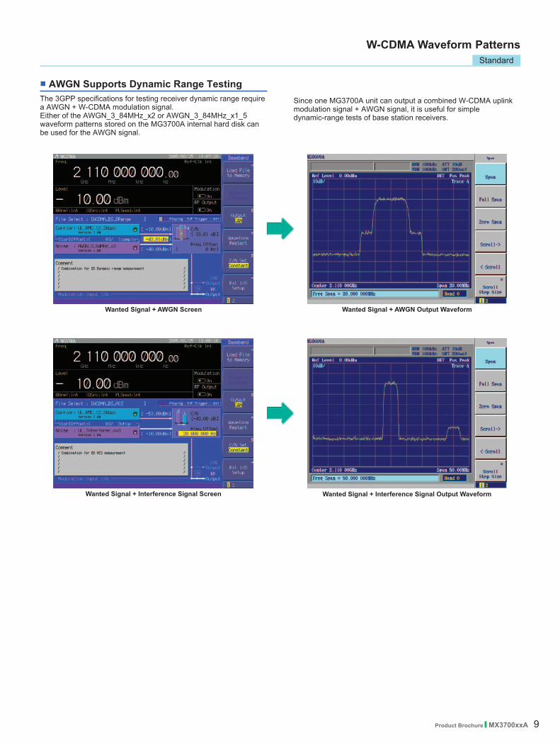
AWGN Supports Dynamic Range TestingThe 3GPP specifications for testing receiver dynamic range require a AWGN + W-CDMA modulation signal.Either of the AWGN_3_84MHz_x2 or AWGN_3_84MHz_x1_5 waveform patterns stored on the MG3700A internal hard disk can be used for the AWGN signal.
Since one MG3700A unit can output a combined W-CDMA uplink modulation signal + AWGN signal, it is useful for simple dynamic-range tests of base station receivers.
Wanted Signal + AWGN Screen Wanted Signal + AWGN Output Waveform
Wanted Signal + Interference Signal Screen Wanted Signal + Interference Signal Output Waveform

10 Product Brochure l MX3700xxA
CDMA2000 1xEV-DO Waveform PatternsStandard
CDMA2000 1xEV-DO Waveform PatternsThe CDMA2000 1xEV-DO waveform patterns listed opposite are stored on the MG3700A internal hard disk.The 3GPP2 signals specified for testing receivers and transmitters of CDMA2000 1xEV-DO access networks (base station) and access terminal (AT) are output by selecting one of the 13 forward and 10 reverse data rate patterns.When multi-carrier signals, mixed idle and active signals and/or multi-user signals are required, the optional MX370103A CDMA2000 1xEV-DO IQproducer application, software can be used to set parameters and generate waveform patterns.
Selecting Waveform Pattern
• Access Terminal (AT) Receiver Test CDMA2000 1xEV-DO forward
Baseband filter: IS-95 SPEC +EQ Data: PN15 fix* (excluding FWD-Idle)
FWD_38_4kbps_16slotFWD_76_8kbps_8slotFWD_153_6kbps_4slotFWD_307_2kbps_2slotFWD_614_4kbps_1slotFWD_307_2kbps_4slotFWD_614_4kbps_2slotFWD_1228_8kbps_1slotFWD_921_6kbps_2slotFWD_1843_2kbps_1slotFWD_1228_8kbps_2slotFWD_2457_6kbps_1slotFWD_Idle
• Access Network (AN) Receiver Test CDMA2000 1xEV-DO Reverse
Baseband filter: IS-95 SPEC Data: PN9 fix*
RVS_9_6kbps_RXRVS_19_2kbps_RXRVS_38_4kbps_RXRVS_76_8kbps_RXRVS_153_6kbps_RXRVS_9_6kbps_TXRVS_19_2kbps_TXRVS_38_4kbps_TXRVS_76_8kbps_RTRVS_153_6kbps_RT
*: This displays the delimited PN sequence for each packet. Therefore, the PN sequence is discontinuous between the end data of one packet and the header data of the next packet.
• Access Terminal (AT) Receiver Test3GPP2 C.S0033 standard receiver tests (PER: Packet Error Rate) can be performed by selecting a forward signal pattern for testing the AT. Since protocols are not supported for the access network simulator and all transmission channels are traffic, while all other channels (Sync, etc.) are unsupported., an external controller (PC) must be used to control the AT and calculate the PER.

Product Brochure l MX3700xxA 11
CDMA2000 1xEV-DO Waveform PatternsStandard
• Access Network (AN) Receiver TestGPP2 C.S0032 standard receiver tests (PER: Packet Error Rate) can be performed by selecting a reverse signal pattern required for testing the AN. Since access terminal simulator protocols are unsupported, an external controller must be used to control the AN and calculate PER.
* Trigger: Timing for synchronizing start of frame (frame trigger)* Clock: Clock for synchronizing chip rate of 1.2288 Mcps (11 x 1.2288 MHz or 5 MHz/10 MHz)
AWGN Supports Dynamic Range TestingThe 3GPP2 specifications require a 1xEV-DO modulation signal + AWGN for performing the receiver dynamic range test.Either of the AWGN_1.23MHz_x2 or AWGN_1.23MHz_x1_5 waveform patterns stored on the MG3700A internal hard disk can be used for the AWGN signal.
Wanted Signal + AWGN Screen Wanted Signal + AWGN Output Waveform
Since one MG3700A unit can output a combined CDMA2000 uplink modulation signal + AWGN signal, it is useful for simple dynamic-range tests of an AN receiver.

12 Product Brochure l MX3700xxA
CDMA2000 Waveform PatternsStandard
CDMA2000 Waveform PatternsThe CDMA2000 waveform patterns listed in the table below are stored on the MG3700A internal hard disk.The 3GPP2 C.S0002-0-2-specified CDMA2000 modulation signals are output by selecting one of these CDMA2000 waveform patterns.Reverse channel signals are output by channel coding (convolutional coding, etc.) 4-frame length PN9 fix*1 data, which is useful for measuring the Frame Error Rate (FER)*2 of base stations and evaluating devices.*1: Since the data length is not an integer multiple of the PN sequence length
(511 bits for PN9), the PN sequence becomes discontinuous at the end.*2: This is the case when the timing signal and 1.2288 Mcps x 11 clock
signal (or 5 or 10 MHz reference clock) can be input from the test target base station to the MG3700A in order to synchronize the frame start point and chip clock.
Selecting Waveform Pattern
Waveform Patterns System Frame Coding Symbol DataRVS_RC1_FCH CDMA2000 1XRTT RC1 Reverse Coded FCH 9.6 kbpsRVS_RC2_FCH CDMA2000 1XRTT RC2 Reverse Coded FCH 14.4 kbpsRVS_RC3_FCH CDMA2000 1XRTT RC3 Reverse Coded PICH, FCH 9.6 kbps RVS_RC3_FCH_SCH CDMA2000 1XRTT RC3 Reverse Coded PICH, FCH 9.6 kbps, SCH 9.6 kbpsRVS_RC3_DCCH CDMA2000 1XRTT RC3 Reverse Coded PICH, DCCH 9.6 kbps RVS_RC4_FCH CDMA2000 1XRTT RC4 Reverse Coded PICH, FCH 14.4 kbpsFWD_RC1-2_9channel CDMA2000 1XRTT RC1, RC2 Forward Spreading only PICH, SyncCH, PagingCH, FCH 19.2 ksps x 6FWD_RC3-5_9channel CDMA2000 1XRTT RC3, RC4, RC5 Forward Spreading only PICH, SyncCH, PagingCH, FCH 38.4 ksps x 6
Waveform Patterns Walsh Code Code Power Data Rate DataRVS_RC1_FCH R-FCH 9.6 kbps PN9fix*
RVS_RC2_FCH R-FCH 14.4 kbps PN9fix*
RVS_RC3_FCH R-PICHR-FCH
04
–5.278 dB–1.528 dB
N/A9.6 kbps
All“0”PN9fix*
RVS_RC3_FCH_SCHR-PICHR-FCHR-SCH
042
–7.5912 dB–3.8412 dB–3.8412 dB
N/A9.6 kbps9.6 kbps
All“0”PN9fix*
PN9fix*
RVS_RC3_DCCH R-PICHR-DCCH
08
–5.278 dB–1.528 dB
N/A9.6 kbps
All“0”PN9fix*
RVS_RC4_FCH R-PICHR-FCH
04
–5.278 dB–1.528 dB
N/A14.4 kbps
All“0”PN9fix*
Waveform Patterns Walsh Code Code Power Symbol Rate Symbol Data
FWD_RC1-2_9channel
F-PICHF-SyncCHPagingCHF-FCH x6
0321
8−13
–7.0 dB–13.3 dB–7.3 dB
–10.3 dB
N/A4.8 kbps
19.2 kbps19.2 kbps
All“0”PN9fix*
PN9fix*
PN9fix*
FWD_RC3-5_9channel
F-PICHF-SyncCHPagingCHF-FCH x6
0321
8−13
–7.0 dB–13.3 dB–7.3 dB
–10.3 dB
N/A4.8 kbps
19.2 kbps38.4 kbps
All“0”PN9fix*
PN9fix*
PN9fix*
R-PICH (Reverse Pilot Channel)R-FCH (Reverse Fundamental Channel)R-SCH (Reverse Supplemental Channel)R-DCCH (Reverse Dedicated Control Channel)F-PICH (Forward Pilot Channel)F-SyncCH (Forward Sync Channel)PagingCH (Paging Channel)F-FCH (Forward Fundamental Channel)

Product Brochure l MX3700xxA 13
GSM/EDGE Waveform PatternsStandard
GSM/EDGE Waveform PatternsThe GSM/EDGE waveform patterns listed in the table below are installed on the internal hard disk when MG3700A Vector Signal Generator is installed. Details for the pattern files are given below.Signals for testing receivers and for evaluating devices in a GSM/EDGE system are output by selecting one of these GSM/EDGE waveform patterns.
• GMSK_PN9, 8PSK_PN9PN9 data which doesn't have slot format is inserted.
• GMSK_TN0, 8PSK_TN0PN9 data is inserted into the entire area of the slots, except the guard. The PN9 data in each slot is continuous.
• NB_GMSK, NB_ALL_GMSK, NB_8PSK, NB_ALL_8PSKPN9 data is inserted into the normal burst encrypted bit area.The PN9 data in the slots is continuous.
• TCH_FSSupports Speech channel at full rate (TCH/FS) specified in Section 3.1 of 3GPP TS05.03
• CS-1_1 (4)_SLOT (_4SLOT )Supports packet data block type 1 (CS-4) and 4 (CS-1) specified in Section 5.1 of 3GPP TS05.03
• DL (UL)_MCS-1 (5, 9)_1SLOT (_4SLOT)Supports packet data block types 5 (MCS-1), 9 (MCS-5), and 13 (MCS-9) specified in Section 5.1 of 3GPP TS05.03
Selecting Waveform Pattern
Waveform Patterns Uplink/Downlink Data Output Slot CommunicationsGMSK_PN9 Uplink/Downlink
PN9*1 – –8PSK_PN9 Uplink/Downlink – –GMSK_TN0 Uplink/Downlink
PN9*2 TN0 –8PSK_TN0 Uplink/Downlink TN0 –NB_GMSK Uplink/Downlink
PN9*3
TN0
GSM
NB_ALL_GMSK Uplink/Downlink All SlotsNB_8PSK Uplink/Downlink TN0NB_ALL_8PSK Uplink/Downlink All SlotsTCH_FS Uplink/Downlink
PN9*4
TN0CS-1_1SLOT Uplink/Downlink TN0CS-4_1SLOT Uplink/Downlink TN0DL_MCS-1_1SLOT Uplink/Downlink TN0
GPRSUL_MCS-1_1SLOT Uplink/Downlink TN0DL_MCS-5_1SLOT Uplink/Downlink TN0
EDGE
UL_MCS-5_1SLOT Uplink/Downlink TN0DL_MCS-9_1SLOT Uplink/Downlink TN0UL_MCS-9_1SLOT Uplink/Downlink TN0DL_MCS-9_4SLOT Uplink/Downlink TN0, 1, 2, 3UL_MCS-9_4SLOT Uplink/Downlink TN0, 1, 2, 3
*1: PN9 data is inserted into the entire area that does not have the slot format.*2: PN9 data is inserted into the entire area of the slots, except the guard.*3: PN9 data is inserted into the normal burst encrypted bit area.*4: The bit string channel-coded for PN9 data is inserted into the normal burst encrypted bit area.
14 Product Brochure l MX3700xxA
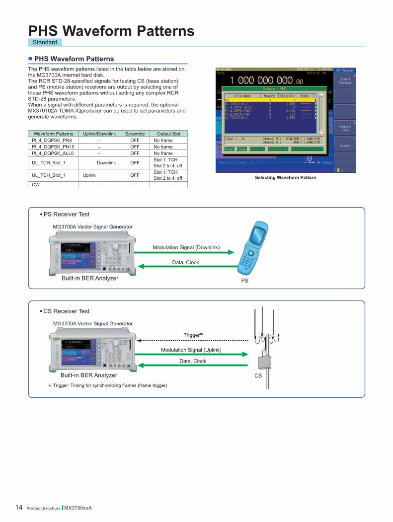
PHS Waveform PatternsStandard
PHS Waveform PatternsThe PHS waveform patterns listed in the table below are stored on the MG3700A internal hard disk.The RCR STD-28-specified signals for testing CS (base station) and PS (mobile station) receivers are output by selecting one of these PHS waveform patterns without setting any complex RCR STD-28 parameters.When a signal with different parameters is required, the optional MX370102A TDMA IQproducer can be used to set parameters and generate waveforms.
Waveform Patterns Uplink/Downlink Scramble Output SlotPI_4_DQPSK_PN9 – OFF No framePI_4_DQPSK_PN15 – OFF No framePI_4_DQPSK_ALL0 – OFF No frame
DL_TCH_Slot_1 Uplink/Downlink OFF Slot 1: TCH Slot 2 to 4: off
UL_TCH_Slot_1 Uplink/Downlink OFF Slot 1: TCH Slot 2 to 4: off
CW – – –Selecting Waveform Pattern
* Trigger: Timing for synchronizing frames (frame trigger)

Product Brochure l MX3700xxA 15
PDC Waveform PatternsStandard
PDC Waveform PatternsWaveform patterns for the Wanted Signals and Interference Signals required to execute the ARIB STD-27-specified transmission and reception tests are stored on the MG3700A internal hard disk. and can be output without requiring options (but check the parameters on the next page first).Waveform patterns to output uplink/downlink Slot 0 data only and unframed waveform pattern for interference signals are provided for full rate and half rate.When a signal with different parameters is required, the optional MX370102A TDMA IQproducer can be used to set parameters and generate waveforms.
Selecting Waveform Pattern
Waveform Patterns Uplink/Downlink Half Rate/Full Rate Output Slot EvaluationPI_4_DQPSK_PN9 – – No frame TX Device TestPI_4_DQPSK_PN15 – – No frame Interfering SignalDL_Full_Rate_Slot0 Uplink/Downlink Full rate Slot 0 only
Wanted Signal for Receiver Test
DL_Half_Rate_Slot0 Uplink/Downlink Half rate Slot 0 onlyUL_Full_Rate_Slot0 Uplink/Downlink Full rate Slot 0 onlyUL_Half_Rate_Slot0 Uplink/Downlink Half rate Slot 0 onlyCW – – – Interfering Signal

16 Product Brochure l MX3700xxA
PDC Packet Waveform PatternsStandard
PDC Packet Waveform PatternsThe four waveform patterns listed in the table below are stored on the MG3700A internal hard disk.The RCR STD-27-specified signals for testing base station and mobile station receivers for UPCH communications can be output by selecting one of these waveform patterns without setting any complex RCR STD-27 parameters.In addition, the Downlink3 data rate UPCH pattern and Uplink1 UPCH pattern can be switched.When a signal with different parameters is required, the optional MX370102A TDMA IQproducer can be used to set parameters and generate waveforms.
Waveform Patterns Uplink/Downlink Output Slot
DL_Packet_Slot_0 Uplink/DownlinkSlot 0=UPCHSlot 1=IDLE (all "1")Slot 2=IDLE (all "1")
DL_Packet_Slot_01 Uplink/DownlinkSlot 0=UPCHSlot 1=UPCHSlot 2=IDLE (all "1")
DL_Packet_Slot_all Uplink/DownlinkSlot 0=UPCHSlot 1=UPCHSlot 2=UPCH
UL_Packet_Slot_0 Uplink/DownlinkSlot 0=UPCHSlot 1=Transmit offSlot 2=Transmit off
Selecting Waveform Pattern
* Trigger: Timing for synchronizing sub frames (frame trigger)

Product Brochure l MX3700xxA 17
Digital Broadcast Waveform PatternsStandard
Digital Broadcast Waveform PatternsThe BS/CS/CATV/ISDB-T waveform patterns listed in the table below are stored on the MG3700A internal hard disk and signals for testing devices are output by selecting one of these waveform patterns.There is also a pattern for evaluating ISDB-T video and audio as well as for simple BER measurements.
Waveform Patterns Outline Parameter
BS_1ch Physical layer waveform pattern of digital BS broadcastFor device evaluation
1channel PN23fix*1 Modulation only
Roll-off factor: 0.35Nyquist Bandwidth: 28.86 MHzModulation: QPSK
CS_1ch Physical layer waveform pattern of digital CS broadcastFor device evaluation
Roll-off factor: 0.35Nyquist Bandwidth: 21.096 MHzModulation: QPSK
CATV_AnnexC_1ch Physical layer waveform pattern for CATV (ITU-T J83 Annex C)For device evaluation
Roll-off factor: 0.13Nyquist Bandwidth: 5.274 MHzModulation: 64QAM
ISDBT_1layer_1chPhysical layer waveform pattern for ISDB-TFor device evaluation
1 channel PN23fix*1 Pilot Signal With TMCC
Mode: 3, GI: 1/8A-Layer: 13seg, 64QAM
ISDBT_2layer_1chMode: 3, GI: 1/8A-Layer: 1seg, QPSKB-Layer: 12seg, 64QAM
ISDBT_2layer_MovieWaveform pattern for ISDB-T partial receptionFor evaluating video and audio data of terminals40-frame waveform length
1 channel For video and audio
Mode: 3, GI: 1/8A-Layer: 1seg, QPSK, CR=2/3, TI=2B-Layer: 12seg, 64QAM, CR=7/8, TI=2
ISDBT_2layer_Movie2Mode: 3, GI: 1/8A-Layer: 1seg, QPSK, CR=2/3, TI=4B-Layer: 12seg, 64QAM, CR=3/4, TI=2
ISDBT_2layer_Coded
Waveform pattern for ISDB-T partial receptionFor simple BER measurement.4-frame waveform length
1 channel For simple BER
Mode: 3, GI: 1/8A-Layer: 1seg, QPSK, CR=2/3, TI=2B-Layer: 12seg, 64QAM, CR=7/8, TI=2
ISDBT_QPSK_1_2Mode: 3, GI: 1/8A-Layer: 1seg, QPSK, CR=1/2, TI=0B-Layer: 12seg, 64QAM, CR=7/8, TI=1
ISDBT_QPSK_2_3Mode: 3, GI: 1/8A-Layer: 1seg, QPSK, CR=2/3, TI=0B-Layer: 12seg, 64QAM, CR=7/8, TI=1
ISDBT_16QAM_1_2Mode: 3, GI: 1/8A-Layer: 1seg, 16QAM, CR=1/2, TI=0B-Layer: 12seg, 64QAM, CR=7/8, TI=1
ISDBT_QPSK_2_3_TI4Mode: 3, GI: 1/8A-Layer: 1seg, QPSK, CR=2/3, TI=4B-Layer: 12seg, 64QAM, CR=3/4, TI=2
ISDBTsb_MovieWaveform pattern for ISDB-Tsb partial reception*2
For evaluation video and audio data of terminals.68-frame waveform length
1 channel For video and audio
Mode: 3, GI: 1/8A/B-Layer: QPSK, CR=1/2, TI=4Seg#1 to #5: 8-segment concatenation transmission in 1-segment formatSeg#6 to #8: 8-segment concatenation transmission in 3-segment format
ISDBTsb_QPSK_1_2
Waveform pattern for ISDB-Tsb partial reception*2
For simple BER measurement.4-frame waveform length
1 channel For simple BER
Mode: 3, GI: 1/8A/B-Layer: QPSK, CR=1/2, TI=0Seg#1 to #5: 8-segment concatenation transmission in 1-segment formatSeg#6 to #8: 8-segment concatenation transmission in 3-segment format
ISDBTsb_QPSK_2_3
Mode: 3, GI: 1/8A/B-Layer: QPSK, CR=2/3, TI=0Seg#1 to #5: 8-segment concatenation transmission in 1-segment formatSeg#6 to #8: 8-segment concatenation transmission in 3-segment format
ISDBTsb_16QAM_1_2
Mode: 3, GI: 1/8A/B-Layer: 16QAM, CR=1/2, TI=0Seg#1 to #5: 8-segment concatenation transmission in 1-segment formatSeg#6 to #8: 8-segment concatenation transmission in 3-segment format
*1: The PN sequence is discontinuous at the waveform pattern connection. This cannot be used to measure BER (PN23) although it can be used for simple BER measurement.
*2: It is not guaranteed that any receiver can receive a waveform with this length.

18 Product Brochure l MX3700xxA
WLAN Waveform PatternsStandard
WLAN Waveform PatternsThe WLAN (IEEE802.11a/b/g) waveform patterns listed in the table below are stored on the MG3700A internal hard disk.Signals for testing the receiver and transmitter of a terminal or module can be output by selecting one of these patterns.The waveform patterns shown below are the signals for one packet. When a waveform pattern is selected, the signal is output in an endless loop. To stop the signal at a fixed number of packets, use the IQproducer Combination File Edit function to generate the sequence file first and select it using the MG3700A (see Section 4.8 of the IQproducer manual).
Selecting Waveform Pattern
• IEEE_802.11a/802.11g (ERP-OFDM) Waveform Patterns List
Waveform Patterns Data Rate(Mbps) Modulation Coding Rate Coding Bits per
Sub-carrierCoding Bits perOFDM Symbol
Data Bits perOFDM Symbol
11a_OFDM_6Mbps 6 BPSK 1/2 1 48 2411a_OFDM_9Mbps 9 BPSK 3/4 1 48 3611a_OFDM_9Mbps_PN9*1 9 BPSK 3/4 1 48 3611a_OFDM_12Mbps 12 QPSK 1/2 2 96 4811a_OFDM_18Mbps 18 QPSK 3/4 2 96 7211a_OFDM_18Mbps_PN9*1 18 QPSK 3/4 2 96 7211a_OFDM_24Mbps 24 16QAM 1/2 4 192 9611a_OFDM_36Mbps 36 16QAM 3/4 4 192 14411a_OFDM_36Mbps_PN9*1 36 16QAM 3/4 4 192 14411a_OFDM_48Mbps 48 64QAM 2/3 6 288 19211a_OFDM_54Mbps 54 64QAM 3/4 6 288 21611a_OFDM_54Mbps_PN9*1 54 64QAM 3/4 6 288 21611a_OFDM_54Mbps_ACP*2 54 64QAM 3/4 6 288 216
*1: Continuous PN9 data between PSDUs*2: Improved ACPR
• IEEE_802.11b Waveform Patterns ListWaveform Patterns Spreading, Coding Modulation
11b_DSSS_1Mbps DSSS, 11 chip Barker Code DBPSK11b_DSSS_2Mbps DSSS, 11 chip Barker Code DQPSK11b_DSSS_2Mbps_PN9*1 DSSS, 11 chip Barker Code DQPSK11b_CCK_5_5Mbps CCK DQPSK11b_CCK_11Mbps CCK DQPSK11b_CCK_11Mbps_PN9*1 CCK DQPSK11b_CCK_11Mbps_ACP*2 CCK DQPSK
• IEEE_802.11g (DSSS-OFDM) Waveform Patterns List
Waveform Patterns Data Rate(Mbps) Modulation Coding Rate Coding Bits per
Sub-carrierCoding Bits perOFDM Symbol
Data Bits perOFDM Symbol
11g_DSSS_OFDM_6Mbps 6 BPSK 1/2 1 48 2411g_DSSS_OFDM_9Mbps 9 BPSK 3/4 1 48 3611g_DSSS_OFDM_12Mbps 12 QPSK 1/2 2 96 4811g_DSSS_OFDM_18Mbps 18 QPSK 3/4 2 96 7211g_DSSS_OFDM_24Mbps 24 16QAM 1/2 4 192 9611g_DSSS_OFDM_36Mbps 36 16QAM 3/4 4 192 14411g_DSSS_OFDM_48Mbps 48 64QAM 2/3 6 288 19211g_DSSS_OFDM_54Mbps 54 64QAM 3/4 6 288 216

Product Brochure l MX3700xxA 19
Bluetooth Waveform PatternsStandard
Waveform Timing Chart
Bluetooth Waveform PatternsThe Bluetooth waveform patterns listed in the table below are stored on the MG3700A internal hard disk.Selecting one of these waveform patterns outputs the best signal for the evaluation.
• POLL:This is used for operation checks and PER measurement of mobile terminals with Bluetooth.
• No Packet Format (PN9, PN15):This is used for BER measurement of mobile terminals and modules with Bluetooth.
• DH1, DH3, DH5:This is used in combination with an external demodulator for loop-back tests (no FEC) of mobile terminals and modules with Bluetooth.
*1: PN9 data is inserted into the payload body.*2: PN9 data is inserted into all areas that do not have a packet format.*3: PN15 data is inserted into all areas that do not have a packet format.*4: Modulation index=0.32*5: Bandwidth time (BT)=0.5*6: Roll-off rate ß=0.4
Waveform Pattern Name Data Rate (Mbits/s) Modulation for Payload Filter Packet Type Dirty, FM File Size [MB]DH1*1 1 GFSK*4 Gaussian*5 DH1 – 0.1 DH3*1 1 GFSK*4 Gaussian*5 DH3 – 0.2 DH5*1 1 GFSK*4 Gaussian*5 DH5 – 0.3 DH3_3SlotOff*1 1 GFSK*4 Gaussian*5 DH3 – 0.2 DH5_5SlotOff*1 1 GFSK*4 Gaussian*5 DH5 – 0.3 POLL 1 GFSK*4 Gaussian*5 POLL – 0.1 2-DH1*1 2 π/4-DQPSK Root Nyquist*6 2-DH1 – 0.1 2-DH3*1 2 π/4-DQPSK Root Nyquist*6 2-DH3 – 0.2 2-DH5*1 2 π/4-DQPSK Root Nyquist*6 2-DH5 – 0.3 2-DH3_3SlotOff*1 2 π/4-DQPSK Root Nyquist*6 2-DH3 – 0.2 2-DH5_5SlotOff*1 2 π/4-DQPSK Root Nyquist*6 2-DH5 – 0.3 3-DH1*1 3 8-DPSK Root Nyquist*6 3-DH1 – 0.1 3-DH3*1 3 8-DPSK Root Nyquist*6 3-DH3 – 0.2 3-DH5*1 3 8-DPSK Root Nyquist*6 3-DH5 – 0.3 3-DH3_3SlotOff*1 3 8-DPSK Root Nyquist*6 3-DH3 – 0.2 3-DH5_5SlotOff*1 3 8-DPSK Root Nyquist*6 3-DH5 – 0.3 GFSK-PN9*2 1 GFSK*4 Gaussian*5 No Packet Format – 0.6 GFSK-PN15*3 1 GFSK*4 Gaussian*5 No Packet Format – 37.5 PI_4_DQPSK-PN9*2 2 π/4-DQPSK Root Nyquist*6 No Packet Format – 0.1 PI_4_DQPSK-PN15*3 2 π/4-DQPSK Root Nyquist*6 No Packet Format – 6.0 8DPSK-PN9*2 3 8-DPSK Root Nyquist*6 No Packet Format – 0.2 8DPSK-PN15*3 3 8-DPSK Root Nyquist*6 No Packet Format – 12.0 DH1_dirty*1 1 GFSK*4 Gaussian*5 DH1 Dirty 9.2 DH3_dirty*1 1 GFSK*4 Gaussian*5 DH3 Dirty 9.2 DH5_dirty*1 1 GFSK*4 Gaussian*5 DH5 Dirty 9.2 2-DH1_dirty*1 2 π/4-DQPSK Root Nyquist*6 2-DH1 Dirty 3.5 2-DH3_dirty*1 2 π/4-DQPSK Root Nyquist*6 2-DH3 Dirty 10.3 2-DH5_dirty*1 2 π/4-DQPSK Root Nyquist*6 2-DH5 Dirty 17.2 3-DH1_dirty*1 3 8-DPSK Root Nyquist*6 3-DH1 Dirty 3.5 3-DH3_dirty*1 3 8-DPSK Root Nyquist*6 3-DH3 Dirty 10.3 3-DH5_dirty*1 3 8-DPSK Root Nyquist*6 3-DH5 Dirty 17.2 DH1_Dirty_withFM*1 1 GFSK*4 Gaussian*5 DH1 Dirty, FM 9.2 DH3_Dirty_withFM*1 1 GFSK*4 Gaussian*5 DH3 Dirty, FM 9.2 DH5_Dirty_withFM*1 1 GFSK*4 Gaussian*5 DH5 Dirty, FM 9.2 2-DH1_Dirty_withFM*1 2 π/4-DQPSK Root Nyquist*6 2-DH1 Dirty, FM 3.52-DH3_Dirty_withFM*1 2 π/4-DQPSK Root Nyquist*6 2-DH3 Dirty, FM 10.3 2-DH5_Dirty_withFM*1 2 π/4-DQPSK Root Nyquist*6 2-DH5 Dirty, FM 17.2 3-DH1_Dirty_withFM*1 3 8-DPSK Root Nyquist*6 3-DH1 Dirty, FM 3.5 3-DH3_Dirty_withFM*1 3 8-DPSK Root Nyquist*6 3-DH3 Dirty, FM 10.3 3-DH5_Dirty_withFM*1 3 8-DPSK Root Nyquist*6 3-DH5 Dirty, FM 17.2 BLE*1 1 GFSK*8 Gaussian*5 BLE Reference Signal – 0.1 BLE_Dirty*1 1 GFSK*8 Gaussian*5 BLE Reference Signal Dirty 28.7 BLE_Dirty_withFM*1 1 GFSK*8 Gaussian*5 BLE Reference Signal Dirty, FM 28.7 BLE_CRC_corrupted*1, *7 1 GFSK*8 Gaussian*5 BLE Reference Signal – 0.2 GFSK-PN15_BLE*3 1 GFSK*8 Gaussian*5 No Packet Format – 6.0
*7: Use in RF-PHY.TS/4.0.0 RCV-LE/CA/07/C (PER Report Integrity) with intentional CRC errors in every other packet is assumed.
*8: Modulation index = 0.5
* Since the recorded file size is rounded up to the nearest 0.1 MB, the true file size may be smaller. Consider this when selecting the ARB memory upgrade option

20 Product Brochure l MX3700xxA
GPS Waveform PatternsStandard
GPS Waveform PatternsThe four GPS waveform patterns listed below are stored on the MG3700A internal hard disk.Selecting one of these waveform patterns outputs the best signal for the evaluation.
• SYNC_ADJThis is used for synchronization adjustment of mobile terminals with GPS.
• TLM, TLM_PARITYThis is used for receiver sensitivity measurement and operation checks of mobile terminals with GPS.
• PARITYThis is used for detecting the parity of mobile terminals with GPS.
• PN9This is used for BER measurement during device evaluation. Selecting Waveform Pattern
Waveform Patterns Main Usage Outline of Data
SYNC_ADJ*1 Synchronization adjustment*2
Consists of TLM, HOW, and default navigation data, formatted according to subframe configuration prescribed in GLOBAL POSITIONING SYSTEM STANDARD POSITIONING SERVICE SIGNAL SPECIFICATION
TLM*3 Sensitivity test Consists of TLM, HOW, and default navigation data, formatted according to subframe configuration prescribed in GLOBAL POSITIONING SYSTEM STANDARD POSITIONING SERVICE SIGNAL SPECIFICATION
PN9 BER measurement Consecutive PN9 data not configured in subframe format
PARITY Parity detectionConfigured in Word format prescribed in GLOBAL POSITIONING SYSTEM STANDARD POSITIONING SERVICE SIGNAL SPECIFICATION One Word consists of 24-bit PN9 fix data and 6-bit parity bit data.
TLM_PARITY Sensitivity test
Consists of TLM, HOW, and Nav Data, formatted according to subframe configuration prescribed in GLOBAL POSITIONING SYSTEM STANDARD POSITIONING SERVICE SIGNAL SPECIFICATION. Random data is inserted into the Nav Data part of Word3 to Word10. One period is configured with 5 subframes.
Data0, Data1, Data10, Data1C
Synchronization adjustment
Used in combination with SYNC_ADJ. These waveform patterns are automatically loaded into the memory when SYNC_ADJ is loaded into the memory. Users do not have to perform loading and selecting of these waveform patterns, because these waveform patterns are automatically selected when SYNC_ADJ is selected.
*1: Use SYNC_ADJ in combination with Data0, Data1, and Data10. When selecting a file, press the Baseband key on the MG3700A to set Pattern Combination to Defined. Refer to the MG3700A Vector Signal Generator Operation Manual (main frame) for details about how to make the settings.
*2: The repeatability of the subframe output timing of the RF output versus external start trigger input is reduced to 10 ns max.*3: When executing a Doppler test, change the RF frequency and sampling clock at the same rate.
The sampling clock when the Doppler frequency is 0 Hz is 4.092 MHz. For example, when applying a +4 kHz Doppler frequency, the following expression establishes (providing the sampling clock as "CLK"): (1575.42 MHz + 4 kHz)/1575.42 MHz = CLK/4.092 MHz then: CLK = 4.09201039 MHz. Refer to the MG3700A Operation Manual (Mainframe) for RF frequency and sampling clock settings.
SYNC_ADJ output timing

Product Brochure l MX3700xxA 21
MX370001A TD-SCDMA Waveform Pattern TD-SCDMA Waveform PatternsSignals for the 3GPP 1.28 Mcps TDD options can be output by installing the MX370001A TD-SCDMA Waveform Pattern option in the MG3700A.
Simple Operation and Fast Signal Pattern Change
Typical waveforms specified in 3GPP, such as the reference management channel, are output just by selecting the waveform pattern stored on the MG3700A internal hard disk without setting any complex TD-SCDMA parameters.• For Evaluating BS Transmitter
BS_DL RMC 1CodeBS_DL RMC 1Code+P-CCPCHBS_DL RMC 8CodeBS_DL RMC 10Code
• For Evaluating BS Receiver BS_UL RMC 12.2kbps (Single)BS_UL RMC 12.2kbps+OCNSBS_UL RMC 64kbps+OCNSBS_UL RMC 144kbps+OCNSBS_UL RMC 384kbps
• For Evaluating UE ReceiverUE_DL RMC 12.2kbpsUE_DL RMC 12.2kbps+OCNSUE_DL RMC 64kbps+OCNSUE_DL RMC 144kbps+OCNSUE_DL RMC 384kbps
• Waveform Patterns for Evaluating BS Transmitters
TargetBS Transmitter Test (DL)
BSTest Signal BS-DL RMC
Waveform Patterns rmc_1 code_bs_dl rmc_P-CCPCH_bs_dl rmc_8 code_bs_dl rmc_10 code_bs_dl
Test Freq/Power Ctrl/ Minimum Pwr P-CCPCH Pwr
OBW/OnOffRatio/ Max Pwr/spurious/
ACLR/TxIM
EVM/ Peak code domain err
Standard TS 25.142DwPTS/UpPTSSYNC_DL/ULNUMBER (quadruples)
SYNC_DL #0(S1)
SYNC_DL #0(S1)
SYNC_DL #0(S1)
SYNC_DL #0(S1)
P-CCPCH – add – –Scrambling Code 0 0 0 0Midamble ID 0 0 0 0Maximum User (user number) 2 (1) 8 (1) 2 (1) 2 (1)Spread Factor 16 16 16 16TimeSlot Number 4, 5, 6 0 4, 5, 6 4, 5, 6Number of DPCH0 – – 0 0DPCH Channelizaton Codes C (i, 16), i=1 C (i, 16), i=1, 2 C (i, 16),1≤i≤8 C (i, 16), 1≤i≤10DPCH0 Channelizaton Codes – – – –Data: DPCH0 PN9 – PN9 PN9Data: other channel – P-CCPCH: All 0 – –Σ DPCH_Ec/Ior [dB] 0 – 0 0DPCH0_Ec/Ior [dB] – – – –DPCH Channelizaton Codes Power [dB]/1 ch 0 – –9 –10
DPCH0 Channelizaton Codes Power [dB]/1 ch – – – –
Optional

22 Product Brochure l MX3700xxA
MX370001A TD-SCDMA Waveform PatternOptional
• Waveform Patterns for Evaluating BS Receivers
TargetBS Receive Test (UL)
BSTest Signal BS-UL RMC
Waveform Patterns rmc12_2k_bs_ul rmc12k_ocns_bs_ul rmc64k_ocns_bs_ul rmc144k_bs_ul rmc384k_bs_ul
TestRS/Min. Input Lev./
Dynamic range/ACS/ Blocking/Rx IM
Performance Req. Performance Req. Performance Req. Performance Req.
Standard TS 25.142DwPTS/UpPTS/SYNC_DL/ UL NUMBER (quadruples) – – – – –
P-CCPCH – – – – –Scrambling Code 0 0 0 0 0Midamble ID 0 0 0 0 0Maximum User (user number) 2 (1) 2 (1) 2 (1) 2 (1) 2 (1)
Spread Factor 8 8 2, 8 2, 8 8, 2TimeSlot Number 1 1 1 1, 2 1, 2, 3, 4Number of DPCH 0 4 1 1 0
DPCH Channelizaton Codes C (i, 8), i=1 C (i, 8), i=1 C (i, 2), i=1 C (i, 2), i=1 C (i, 2), i=1 C (i, 8), i=5
DPCH0 Channelizaton Codes – C (i, 8), 2≤i≤5 C (i, 8), i=5 C (i, 8), i=5 –Data: DPCH0 PN9 PN9 PN9 PN9 PN9Data: other channel – PN9 PN9 PN9 –Σ DPCH_Ec/Ior [dB] 0 – – – 0DPCH0_Ec/Ior [dB] – –7 –7 –7 –DPCH Channelizaton Codes Power [dB]/1ch 0 –7 –0.97 –0.97 C (i, 2)=−6.99
C (i, 8)=−0.97DPCH0 Channelizaton Codes Power [dB]/1ch – –7 –7 –7 –
• Waveform Patterns for Evaluating UE Receivers
TargetUE Receiver Test (DL)
UETest Signal UE-DL RMC
Waveform Patterns rmc12_2k_ue_dl rmc12k_ocns_ue_dl rmc64k_ocns_ue_dl rmc144k_ocns_ue_dl rmc384k_ue_dl
TestRS/Min. Input Lev./
ACS/Blocking/ Spur.Resp. /Inter Mod
Maximum input level test/
RMC 12.2kPerformance Req. Performance Req. Performance Req.
Standard TS 25.102DwPTS/UpPTSSYNC_DL/UL NUMBER (quadruples)
SYNC_DL #0(S1)
SYNC_DL #0(S1)
SYNC_DL #0(S1)
SYNC_DL #0(S1)
SYNC_DL #0(S1)
P-CCPCH Add Add Add Add AddScramblng Code 0 0 0 0 0Midamble ID 0 0 0 0 0Maximum User (user number) 8 (1) 8 (1) 8 (1) 8 (1) 8 (1)
Spread Factor 16 16 16 16 16TimeSlot Number 4 4 4 4, 5 3, 4, 5, 6Number of DPCH0 0 8 2 2 0DPCH Channelizaton Codes C (i, 16), i=1,2 C (i,16), i=1, 2 C (i, 16), i=1, …, 8 C (i, 16), i=1, …, 8 C (i, 16), i=1, …, 10
DPCH0 Channelizaton Codes – C (i, 16) 3≤i≤10
C (i, 16) 9≤i≤10
C (i, 16) 9≤i≤10 –
Data: DPCH0 PN9 PN9 PN9 PN9 PN9Data: other channel – PN9 PN9 PN9 –Σ DPCH_Ec/Ior [dB] 0 –7 – – –DPCH0_Ec/Ior [dB] – –10 –10 –10 0DPCH Channelizaton Codes Power [dB]/1ch –3.01 –10.00 –10.00 –10.00 −10
DPCH0 Channelizaton Codes Power [dB]/1ch – –10.00 –10.00 –10.00 –

Product Brochure l MX3700xxA 23
MX370001A TD-SCDMA Waveform PatternOptional
Frame Configuration• UL-RMC12.2 kbps: For BS receiver test (Uplink)TS-25.142: BS UL reference measurement channel p132, A2.1.2, 1.28 Mcps, SF = 8Test items: 7.2 Reference sensitivity level
7.3 Dynamic range 7.4 Adjacent Channel Selectivity (ACS) 7.5 Blocking characteristics 7.6 Intermodulation characteristics
• DL-RMC12.2 kbps: For UE receiver test (Downlink)TS-25.102: UE DL reference measurement channel p58, A.2.2.2.1, 1.28 Mcps, 12.2 kbps, SF = 16Test items: 7.3 Reference sensitivity level
7.4 Maximum input level 7.5 Adjacent Channel selectivity (ACS) 7.6 Blocking characteristics 7.7 Spurious response 7.8 Intermodulation characteristics

24 Product Brochure l MX3700xxA
MX370002A Public Radio System Waveform PatternOptional
Public Radio System Waveform PatternsThe downlink and uplink modulation signals for the following ARIB standards can be output by installing the MX370002A Public Radio System Waveform Pattern option in the MG3700A.
• RCR STD-39Waveform Patterns Uplink/Downlink Transmit Frame
UpLink Uplink/Downlink 0, x, x, xDownLink 1 Uplink/Downlink 0, x, x, xDownLink 4 Uplink/Downlink 0, 1, 2, 3DownCCH 4 Uplink/Downlink 0, 1, 2, 3PN9 – –PN15 – –
Sampling Rate 128 kHzSymbol Rate 16 ksps
• ARIB STD-T61Waveform Patterns Uplink/Downlink Transmit Frame
UpDownLink Uplink/Downlink 040ms_Burst_all Uplink/Downlink 0, 1, 2, 320ms_Burst_all Uplink/Downlink 0, 1, 2, 3, 4, 5, 6, 740ms_Burst_1_4 Uplink/Downlink 0, x, x, x,20ms_Burst_1_8 Uplink/Downlink 0, x, x, x, x, x, x, x40ms_Burst_all_Ramp* Uplink/Downlink 0, 1, 2, 320ms_Burst_all_Ramp* Uplink/Downlink 0, 1, 2, 3, 4, 5, 6, 740ms_Burst_1_4_Ramp* Uplink/Downlink 0, x, x, x,20ms_Burst_1_8_Ramp* Uplink/Downlink 0, x, x, x, x, x, x, xPN9 – –PN15 – –
Sampling Rate 153.6 kHzSymbol Rate 4.8 ksps
*: Waveform pattern names to which _Ramp is appended are in accordance with the ARIB STD-T61 standard. Appending _Ramp to waveforms patterns improves the adjacent-channel leakage-power ratio by lengthening the rise and fall times of the guard time transient response.
Simple Operation and Fast Signal Pattern Change
Signals for the ARIB-specified receiver and transmitter tests are output by selecting the waveform pattern stored on the MG3700A internal hard disk without setting complex ARIB standard parameters.The TCH/CCH, PN9, and PN15 continuous modulation patterns can be switched quickly.
• ARIB STD-T79Waveform Patterns Uplink/Downlink Transmit Frame
UpLink Uplink/Downlink 0, x, x, xDownLink 1 Uplink/Downlink 0, x, x, xDownLink 4 Uplink/Downlink 0, 1, 2, 3Direct Uplink/Downlink 1, x, x, xPN9 – –PN15 – –
Sampling Rate 128 kHzSymbol Rate 16 ksps
• ARIB STD-T86Waveform Patterns Uplink/Downlink Transmit Frame
Up_cch Uplink/Downlink x, x, x, 3, x, xUp_tch Uplink/Downlink x, x, x, 3, x, x Down_tch_all Uplink/Downlink 0, 1, 2, 3, 4, 5Down_cch Uplink/Downlink 0, x, x, x, x, xDown_tch Uplink/Downlink 0, 1, 2, x, 4, 5PN9 – –PN15 – –
Sampling Rate 90 kHzSymbol Rate 11.25 ksps
Product Brochure l MX3700xxA 25
MX370002A Public Radio System Waveform PatternOptional
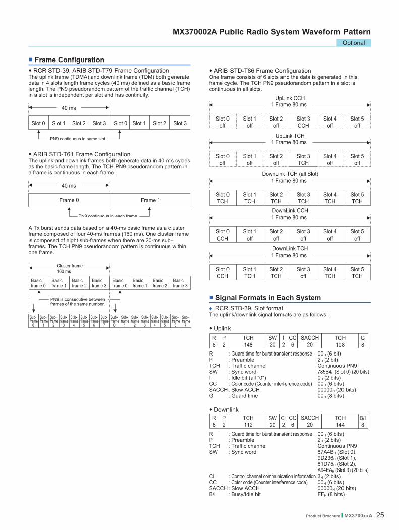
• ARIB STD-T61 Frame ConfigurationThe uplink and downlink frames both generate data in 40-ms cycles as the basic frame length. The TCH PN9 pseudorandom pattern in a frame is continuous in each frame.
A Tx burst sends data based on a 40-ms basic frame as a cluster frame composed of four 40-ms frames (160 ms). One cluster frame is composed of eight sub-frames when there are 20-ms sub-frames. The TCH PN9 pseudorandom pattern is continuous within one frame.
• ARIB STD-T86 Frame ConfigurationOne frame consists of 6 slots and the data is generated in this frame cycle. The TCH PN9 pseudorandom pattern in a slot is continuous in all slots.
Frame Configuration• RCR STD-39, ARIB STD-T79 Frame ConfigurationThe uplink frame (TDMA) and downlink frame (TDM) both generate data in 4 slots length frame cycles (40 ms) defined as a basic frame length. The PN9 pseudorandom pattern of the traffic channel (TCH) in a slot is independent per slot and has continuity.
Signal Formats in Each System♦ RCR STD-39, Slot formatThe uplink/downlink signal formats are as follows:
• Uplink
R : Guard time for burst transient response 00H (6 bits)P : Preamble 2H (2 bits)TCH : Traffic channel Continuous PN9SW : Sync word 87A4BH (Slot 0), 9D236H (Slot 1), 81D75H (Slot 2), A94EAH (Slot 3) (20 bits)CI : Control channel communication information 3H (2 bits)CC : Color code (Counter interference code) 00H (6 bits)SACCH : Slow ACCH 00000H (20 bits)B/I : Busy/Idle bit FFH (8 bits)
R : Guard time for burst transient response 00H (6 bit)P : Preamble 2H (2 bit)TCH : Traffic channel Continuous PN9SW : Sync word 785B4H (Slot 0) (20 bits)I : Idle bit (all "0") 0H (2 bits)CC : Color code (Counter interference code) 00H (6 bits)SACCH : Slow ACCH 00000H (20 bits)G : Guard time 00H (8 bits)
• Downlink

26 Product Brochure l MX3700xxA
R : Ramp time for transient response 0H (16 bits)P : Pilot symbol AH (4 bits)SW : Sync word Uplink=00A000000AH (40 bits) Downlink=00A000AAAAH (40 bits)C : Channel identification 8H (4 bits)TCH : Information channel PN9 pseudo random pattern (The TCH PN pattern is
continuous in all slots.)G : Guard time for transient response 00000H (20 bits)
• Uplink/Downlink control channel
MX370002A Public Radio System Waveform PatternOptional
• Downlink control channel
R : Guard time for burst transient response 00H (6 bits)P : Preamble 2H (2 bits)TCH : Traffic channel Continuous PN9SW : Sync word 87A4BH (Slot 0), 9D236H (Slot 1), 81D75H (Slot 2), A94EAH (Slot 3) (20 bits)CI : Control channel communication information 3H (2 bits)CC : Color code (Counter interference code) 00H (6 bits)SACCH : Slow ACCH 00000H (20 bits)B/I : Busy/Idle bit FFH (8 bits)
• Direct communication between mobile stations
R : Guard time for burst transient response 00H (6 bits)P : Preamble 2H (2 bits)TCH : Traffic channel Continuous PN9SW : Sync word 785B4H (Slot 0) (20 bits)I : Idle bit (all "0") 0H (2 bits)CC : Color code (Counter interference code) 00H (6 bits)SACCH : Slow ACCH 00000H (20 bits)G : Guard time for transient response 00H (8 bits)
R : Guard time for burst transient response 00H (8 bit)SW1 : Sync word 1 1E56FH (20 bit)RICH : Radio information channel 0000000000000H (52 bit)TCH1 : Traffic channel 1 Continuous PN9G : Guard time 0H (4 bit)
• Burst signal (20 ms)
R : Guard time for burst transient response 00H (8 bit)SW2 : Sync word 2 31BAFH (20 bit)TCH2 : Traffic channel 2 Continuous PN9G : Guard time 0H (4 bit)
♦ ARIB STD-T79, Slot formatThe uplink/downlink and direct communication signal formats between mobile stations are as follows:
• Uplink
G : Guard time for transient response 00H (8 bits), 0000H (16 bits)R : Guard time for burst transient response 00H (6 bits)P : Preamble 2H (2 bits)TCH : Traffic channel Continuous PN9SW : Sync word 4D9DEH (20 bits)PICH : Parameter information channel 000H (12 bits)
♦ ARIB STD-T86, Slot formatThere are four types of slots: uplink/downlink traffic channels and uplink/downlink control channels.
• Uplink/Downlink traffic channel
R : Guard time for burst transient response 00H (6 bit)P : Preamble 2H (2 bit)CAC : Control signal Continuous PN9SW : Sync word 87A4BH (Slot 0), 9D236H (Slot 1), 81D75H (Slot 2), A94EAH (Slot 3) (20 bits)CC : Color code (Counter interference code) 00H (6 bit)I : Idle bit 0H (4 bit)
♦ ARIB STD-T61, Frame formatThe uplink/downlink signal formats are as follows:
LP+R : Preamble for linearizer and guard time for burst transient response 00000000H (30 bits)
Pa : Preamble 2H (2 bits)TCH : Traffic channel Continuous PN9RI : Radio information channel 00000000000000H (56 bits)SW : Sync word 1E56FH (20 bits)Undefined : 00000H (20 bits)
• Burst signal (40 ms)
• Downlink
R : Ramp time for transient response 0H (16 bits)AP : Repetition of AGC preamble 20A800080AH
P : Pilot symbol AH (4 bits)SW : Sync word Uplink=000A0AA00AH (40 bits) Downlink=000A0A00A0H (40 bits)C : Channel identification AH (4 bits)CAC : Information channel random patternG : Guard time for transient response 00000H (20 bits)

Product Brochure l MX3700xxA 27
MX370073A DFS Radar PatternOptional
Selecting Waveform Pattern(Example: TELEC Waveform Patterns)
Sequence Function Display
DFS Radar PatternsInstalling the MX370073A DFS Radar Pattern option in the MG3700A Vector Signal Generator supports output of TELEC-T403 and FCC06-96 DFS test signals.Output of complex combinations of pulse, chirp and hopping signals required to support DFS tests is made easy just by selecting combination files supplied with the MX370073A.* DFS: Dynamic Frequency Selection
• One unit supports pulse, chirp and hopping signals.• PC not required. Simply selecting prepared waveform
pattern outputs various signals.
• Setup
• Sequence FunctionThis standard function switches and outputs multiple waveform patterns continuously.Standards-compliant test signals can be created by selecting a combination file combining complex patterns of pulse, chirp, hopping, and null signal waveforms.

28 Product Brochure l MX3700xxA
MX370073A DFS Radar PatternOptional
• TELEC Test Waveform Patterns
Specification No. Package Combination File Name Note File Size [MB]
Appended Table 1
Type 1DFS_behhyoudai1gou-1_2
behhyou_dai1gou-1
Fixed Pulse Radar Signals One pattern each
60
Type 2 behhyou_dai1gou-2
Appended Table 2
Type 1DFS_behhyoudai2gou-1_2_3
behhyou_dai2gou-1Type 2 behhyou_dai2gou-2Type 3 behhyou_dai2gou-3
Type 4 DFS_behhyoudai2gou-4 behhyou2-4-1 to behhyou2-4-40
Variable Pulse Radar Signals Forty patterns eachType 5 DFS_behhyoudai2gou-5 behhyou2-5-1 to
behhyou2-5-40
Type 6 DFS_behhyoudai2gou-6 behhyou2-6-1 to behhyou2-6-40
Appended Table 3 Type 1 DFS_behhyoudai3gou behhyou3-1 to
behhyou3-40Variable Chirp Radar Signals Forty patterns each
Appended Table 4 Type 1
DFS_behhyoudai4gou behhyou4-1 to behhyou4-40
Frequency Hopping Radar Signals Forty patterns each For DUT 20 MHz detection bandwidth
DFS_behhyoudai4gou_40M behhyou4-1_40M to behhyou4-40_40M
Frequency Hopping Radar Signals Forty patterns each For DUT 40 MHz detection bandwidth
• FCC Test Waveform Patterns
Specification No. Package Combination File Name Note File Size [MB]
Short Pulse Radar
Type 1 RadarType1 ShortPulse1 Fixed Pulse Radar Signals One pattern
60
Type 2 RadarType2 ShortPulse2-1 to ShortPulse2-40
Variable Pulse Radar Signals Forty patterns eachType 3 RadarType3 ShortPulse3-1 to
ShortPulse3-40
Type 4 RadarType4 ShortPulse4-1 to ShortPulse4-40
Long Pulse Radar Type 5 RadarType5 LongPulse-1 to
LongPulse-40Variable Chirp Radar Signals Forty patterns each
Frequency Hopping Radar
Type 6
RadarType6_20M Hopping-1_20M to Hopping-40_20M
Frequency Hopping Radar Signals Forty patterns each For 20 MHz DUT detection bandwidth
RadarType6_40M Hopping-1_40M to Hopping-40_40M
Frequency Hopping Radar Signals Forty patterns each For 40 MHz DUT detection bandwidth
* Since the recorded file size is rounded up to the nearest 0.1 MB, the true file size may be smaller. Consider this when selecting the ARB memory upgrade option

Product Brochure l MX3700xxA 29
MX370075A DFS (ETSI) Waveform PatternOptional
DFS (ETSI) Waveform PatternsInstalling the MX370075A DFS (ETSI) Waveform Pattern option in the MG3700A Vector Signal Generator supports output of ETSI EN 301 893 DFS test signals.Output of complex combinations of pulse and chirp signals required to support DFS tests is made easy just by selecting combination files supplied with the MX370075A.* DFS: Dynamic Frequency Selection
• One unit supports pulse and chirp signals.• PC not required. Simply selecting prepared waveform
pattern outputs various signals.
• Setup
• Sequence FunctionThis standard function switches and outputs multiple waveform patterns continuously.Standards-compliant test signals can be created by combining complex patterns of pulse, chirp, and null signal waveforms.Users can output pulse and chirp signals for DFS tests easily just by selecting a combination file with this sequence information.

30 Product Brochure l MX3700xxA
MX370075A DFS (ETSI) Waveform PatternOptional
• ETSI Test Waveform Patterns
Specification No. Package Combination File Name Note File Size [MB]
Reference Signal ReferenceDFSSignal ReferenceDFSsignal Fixed Pulse Radar SignalsOne pattern
600Radar Test Signal
1
TestSignal-1_Single
TestSignal-1_S_00 to TestSignal-1_S_19
Variable Pulse Radar Signals for single burst Twenty patterns
TestSignal-1B_S_00 to TestSignal-1B_S_19
Variable Pulse Radar Signals for single burst Twenty patternsUsed from 5600 MHz to 5650 MHz
TestSignal-1_Multi
TestSignal-1_M_00 to TestSignal-1_M_19
Variable Pulse Radar Signals for multi-burst Twenty patterns
TestSignal-1B_M_00 to TestSignal-1B_M_19
Variable Pulse Radar Signals for multi-burst Twenty patternsUsed from 5600 MHz to 5650 MHz
2
TestSignal-2_Single
TestSignal-2_S_00 to TestSignal-2_S_19
Variable Pulse Radar Signals for single burst Twenty patterns
TestSignal-2B_S_00 to TestSignal-2B_S_19
Variable Pulse Radar Signals for single burst Twenty patternsUsed from 5600 MHz to 5650 MHz
TestSignal-2_Multi
TestSignal-2_M_00 to TestSignal-2_M_19
Variable Pulse Radar Signals for multi-burst Twenty patterns
TestSignal-2B_M_00 to TestSignal-2B_M_19
Variable Pulse Radar Signals for multi-burst Twenty patternsUsed from 5600 MHz to 5650 MHz
3TestSignal-3_Single TestSignal-3_S_00 to
TestSignal-3_S_19Variable Pulse Radar Signals for single burst Twenty patterns
TestSignal-3_Multi TestSignal-3_M_00 to TestSignal-3_M_19
Variable Pulse Radar Signals for multi-burst Twenty patterns
4TestSignal-4_Single TestSignal-4_S_00 to
TestSignal-4_S_19Variable Chirp Radar Signals for multi-burst Twenty patterns
TestSignal-4_Multi TestSignal-4_M_00 to TestSignal-4_M_19
Variable Chirp Radar Signals for multi-burst Twenty patterns
5
TestSignal-5_Single
TestSignal-5_S_00 to TestSignal-5_S_19
Variable Pulse Radar Signals for single burst Twenty patterns
TestSignal-5B_S_00 to TestSignal-5B_S_19
Variable Pulse Radar Signals for single burst Twenty patternsUsed from 5600 MHz to 5650 MHz
TestSignal-5_Multi
TestSignal-5_M_00 to TestSignal-5_M_19
Variable Pulse Radar Signals for multi-burst Twenty patterns
TestSignal-5B_M_00 to TestSignal-5B_M_19
Variable Pulse Radar Signals for multi-burst Twenty patternsUsed from 5600 MHz to 5650 MHz
6
TestSignal-6_Single
TestSignal-6_S_00 to TestSignal-6_S_19
Variable Pulse Radar Signals for single burst Twenty patterns.
TestSignal-6B_S_00 to TestSignal-6B_S_19
Variable Pulse Radar Signals for single burst Twenty patternsUsed from 5600 MHz to 5650 MHz
TestSignal-6_Multi
TestSignal-6_M_00 to TestSignal-6_M_19
Variable Pulse Radar Signals for multi-burst Twenty patterns
TestSignal-6B_M_00 to TestSignal-6B_M_19
Variable Pulse Radar Signals for multi-burst Twenty patternsUsed from 5600 MHz to 5650 MHz
* Since the recorded file size is rounded up to the nearest 0.1 MB, the true file size may be smaller. Consider this when selecting the ARB memory upgrade option

Product Brochure l MX3700xxA 31
Ordering InformationPlease specify model/order number, name, and quantity when ordering.The names listed in the chart below are Order Names. The actual name of the item may differ from the Order Name.
Model/Order No. Name Remarks
MG3700A― Main frame ―Vector Signal Generator
J1276
J1254Z0742
― Standard accessories ―Power Cord: 1 pcLAN Straight Cable: 1 pcCompactFlash: 1 pcCompactFlash Adapter: 1 pcMG3700A CD-ROM: 1 pc
10 cm, For U link connection on Rear panel64 MB or more
Main frame operation manual, IQproducer operation manual, Standard waveform operation manual, IQproducer software
MG3700A-002MG3700A-011MG3700A-021MG3700A-031
― Options ―Mechanical AttenuatorUpper Frequency 6 GHzARB Memory Upgrade 512 MsampleHigh Speed BER Test Function
Changes standard electronic attenuator to mechanical attenuator250 kHz to 3 GHz extended to 250 kHz to 6 GHzExtends standard 128 Msample/channel × 2 to 256 Msample/channel × 2Extends standard BER test function
MG3700A-102MG3700A-103MG3700A-111MG3700A-121MG3700A-131
Mechanical Attenuator RetrofitElectronic Attenuator RetrofitUpper Frequency 6 GHz RetrofitARB Memory Upgrade 512 Msample RetrofitHigh Speed BER Test Function Retrofit
Retrofitted to shipped MG3700ARetrofitted to shipped MG3700ARetrofitted to shipped MG3700ARetrofitted to shipped MG3700ARetrofitted to shipped MG3700A
MG3700A-ES210MG3700A-ES310MG3700A-ES510
― Maintenance service ―Extended Warranty ServiceExtended Warranty ServiceExtended Warranty Service
2 years3 years5 years
MX370001AMX370002AMX370073AMX370075A
MX370101AMX370102AMX370103AMX370104AMX370105AMX370106AMX370107AMX370108AMX370108A-001MX370109AMX370110AMX370110A-001MX370111AMX370111A-001MX370112A
― Softwares (Waveform pattern) ―TD-SCDMA Waveform PatternPublic Radio System Waveform Pattern DFS Radar PatternDFS (ETSI) Waveform Pattern― Softwares (License key for IQproducer system) ―HSDPA/HSUPA IQproducerTDMA IQproducerCDMA2000 1xEV-DO IQproducerMulti-carrier IQproducerMobile WiMAX IQproducerDVB-T/H IQproducerFading IQproducerLTE IQproducerLTE-Advanced FDD OptionXG-PHS IQproducerLTE TDD IQproducerLTE-Advanced TDD OptionWLAN IQproducer802.11ac (80MHz) OptionTD-SCDMA IQproducer
RCR STD-39, ARIB STD-T61/T79/T86WLAN 5.3/5.6 GHz band DFS tests (for TELEC and FCC)WLAN 5.3/5.6 GHz DFS test (ETSI)
Requires MX370108A.
Requires MX370110A.
Requires MX370111A. Only for MG3700A.
Z0777W2495AEW2496AEW2539AEW2533AEW3596AEW3597AEW2503AEW2504AEW2505AEW2633AEW2734AEW2798AEW2995AEW3022AEW3152AEW3221AEW3488AEW3582AEG0141K240BMA1612AMP752AMA2512AJ0576BJ0576DJ0127AJ0127BJ0127CJ0322AJ0322BJ0322CJ0322DJ0004J1261BJ1261DJ0008J1277B0329CB0331CB0332B0333CB0334C
― Optional accessories ―Standard Waveform Pattern Upgrade KitMG3700A Operation Manual (Main Unit)MG3700A Operation Manual (IQproducer)MG3700A Operation Manual (Standard Waveform Pattern)MX370001A Operation ManualMX370073A Operation ManualMX370075A Operation ManualMX370101A Operation ManualMX370102A Operation ManualMX370103A Operation ManualMX370104A Operation ManualMX370105A Operation ManualMX370106A Operation ManualMX370107A Operation ManualMX370108A Operation ManualMX370109A Operation ManualMX370110A Operation ManualMX370111A Operation ManualMX370112A Operation ManualHDD ASSYPower Divider (K connector)Four-port Junction PadTerminationBand Pass FilterCoaxial Cord, 1.0 mCoaxial Cord, 2.0 mCoaxial Cord, 1.0 mCoaxial Cord, 2.0 mCoaxial Cord, 0.5 mCoaxial Cord, 0.5 mCoaxial Cord, 1.0 mCoaxial Cord, 1.5 mCoaxial Cord, 2.0 mCoaxial AdapterEthernet Cable (Shield Type)Ethernet Cable (Shield Type)GPIB Cable, 2.0 mIQ Output Conversion AdapterFront Cover for 1MW 4UFront Panel Handle KitJoint PlateRack Mount KitHardtype Carrying Case
DVD 4 piece sets
TD-SCDMA Waveform PatternDFS Rader Pattern (TELEC and FCC)DFS (ETSI) Waveform PatternHSDPA/HSUPA IQproducerTDMA IQproducerCDMA2000 1xEV-DO IQproducerMulti-carrier IQproducerMobile WiMAX IQproducerDVB-T/H IQproducerFading IQproducerLTE IQproducerXG-PHS IQproducerLTE TDD IQproducerWLAN IQproducerTD-SCDMA IQproducer Hard diskDC to 26.5 GHz, K-J, 50Ω, 1 Wmax5 MHz to 3 GHz, N-JDC to 12.4 GHz, 50Ω, N-PFor W-CDMA, Pass band: 1.92 GHz to 2.17 GHzN-P · 5D-2W · N-PN-P · 5D-2W · N-PBNC-P · RG-58A/U · BNC-PBNC-P · RG-58A/U · BNC-PBNC-P · RG-58A/U · BNC-PSMA-P · SMA-P, DC to 18 GHz, 50ΩSMA-P · SMA-P, DC to 18 GHz, 50ΩSMA-P · SMA-P, DC to 18 GHz, 50ΩSMA-P · SMA-P, DC to 18 GHz, 50ΩN-P · SMA-J Conversion Adapter, DC to 12.4 GHzStraight-through, 3 mCross, 3 m
D-Sub/BNC
2 pcs/set4 pcs/setEIAWith Front cover and Casters

• United StatesAnritsu Company1155 East Collins Blvd., Suite 100, Richardson, TX 75081, U.S.A.Toll Free: 1-800-267-4878Phone: +1-972-644-1777Fax: +1-972-671-1877
• CanadaAnritsu Electronics Ltd.700 Silver Seven Road, Suite 120, Kanata, Ontario K2V 1C3, CanadaPhone: +1-613-591-2003 Fax: +1-613-591-1006
• Brazil Anritsu Eletrônica Ltda.Praça Amadeu Amaral, 27 - 1 Andar01327-010 - Bela Vista - São Paulo - SP - BrazilPhone: +55-11-3283-2511Fax: +55-11-3288-6940
• MexicoAnritsu Company, S.A. de C.V.Av. Ejército Nacional No. 579 Piso 9, Col. Granada11520 México, D.F., MéxicoPhone: +52-55-1101-2370Fax: +52-55-5254-3147
• United KingdomAnritsu EMEA Ltd.200 Capability Green, Luton, Bedfordshire, LU1 3LU, U.K.Phone: +44-1582-433200 Fax: +44-1582-731303
• FranceAnritsu S.A.12 avenue du Québec, Bâtiment Iris 1- Silic 612,91140 VILLEBON SUR YVETTE, FrancePhone: +33-1-60-92-15-50Fax: +33-1-64-46-10-65
• GermanyAnritsu GmbHNemetschek Haus, Konrad-Zuse-Platz 1 81829 München, Germany Phone: +49-89-442308-0 Fax: +49-89-442308-55
• ItalyAnritsu S.r.l.Via Elio Vittorini 129, 00144 Roma, ItalyPhone: +39-6-509-9711 Fax: +39-6-502-2425
• SwedenAnritsu ABBorgarfjordsgatan 13A, 164 40 KISTA, SwedenPhone: +46-8-534-707-00 Fax: +46-8-534-707-30
• FinlandAnritsu ABTeknobulevardi 3-5, FI-01530 VANTAA, FinlandPhone: +358-20-741-8100Fax: +358-20-741-8111
• DenmarkAnritsu A/S (Service Assurance)Anritsu AB (Test & Measurement)Kay Fiskers Plads 9, 2300 Copenhagen S, DenmarkPhone: +45-7211-2200Fax: +45-7211-2210
• RussiaAnritsu EMEA Ltd. Representation Office in RussiaTverskaya str. 16/2, bld. 1, 7th floor.Russia, 125009, MoscowPhone: +7-495-363-1694Fax: +7-495-935-8962
• United Arab EmiratesAnritsu EMEA Ltd.Dubai Liaison OfficeP O Box 500413 - Dubai Internet CityAl Thuraya Building, Tower 1, Suit 701, 7th FloorDubai, United Arab EmiratesPhone: +971-4-3670352Fax: +971-4-3688460
• IndiaAnritsu India Private Limited2nd & 3rd Floor, #837/1, Binnamangla 1st Stage, Indiranagar, 100ft Road, Bangalore - 560038, IndiaPhone: +91-80-4058-1300Fax: +91-80-4058-1301
• SingaporeAnritsu Pte. Ltd.60 Alexandra Terrace, #02-08, The Comtech (Lobby A)Singapore 118502Phone: +65-6282-2400Fax: +65-6282-2533
• P.R. China (Shanghai)Anritsu (China) Co., Ltd.Room 1715, Tower A CITY CENTER of Shanghai, No.100 Zunyi Road, Chang Ning District, Shanghai 200051, P.R. ChinaPhone: +86-21-6237-0898Fax: +86-21-6237-0899
• P.R. China (Hong Kong)Anritsu Company Ltd.Unit 1006-7, 10/F., Greenfield Tower, Concordia Plaza,No. 1 Science Museum Road, Tsim Sha Tsui East, Kowloon, Hong Kong, P.R. ChinaPhone: +852-2301-4980Fax: +852-2301-3545
• JapanAnritsu Corporation8-5, Tamura-cho, Atsugi-shi, Kanagawa, 243-0016 JapanPhone: +81-46-296-1221Fax: +81-46-296-1238
• KoreaAnritsu Corporation, Ltd.502, 5FL H-Square N B/D, 681Sampyeong-dong, Bundang-gu, Seongnam-si, Gyeonggi-do, 463-400 KoreaPhone: +82-31-696-7750Fax: +82-31-696-7751
• AustraliaAnritsu Pty. Ltd.Unit 21/270 Ferntree Gully Road, Notting Hill, Victoria 3168, AustraliaPhone: +61-3-9558-8177Fax: +61-3-9558-8255
• TaiwanAnritsu Company Inc.7F, No. 316, Sec. 1, NeiHu Rd., Taipei 114, TaiwanPhone: +886-2-8751-1816Fax: +886-2-8751-1817
Specifications are subject to change without notice.
1209
Printed on Recycled Paper Catalog No. MX3700xxA-E-A-1-(16.00) Printed in Japan 18/MAR/2013 ddcm/CDT
• IQproducer™ is a registered trademark of Anritsu Corporation.• MATLAB® is a registered trademark of The MathWorks, Inc.• CDMA2000® is a registered trademark of the Telecommunications Industry Association (TIA-USA).• The Bluetooth® mark and logos are owned by Bluetooth SIG, Inc. and are used by Anritsu under license.• Pentium® is registered trademarks of Intel Corporation or its subsidiaries in the USA and other countries.• Windows® is a registered trademark of Microsoft Corporation in the USA and other countries.• CompactFlash® is a registered trademark of SanDisk Corporation in the United States and is licensed to CFA (Compact Flash Association).• WiMAX® is a trademark or registered trademark of WiMAX Forum.• Other companies, product names and service names are registered trademarks of their respective companies.