bounding and reducing memory interference in cots-based ... · bounding and reducing memory...
TRANSCRIPT
Bounding and Reducing Memory Interference in
COTS-based Multi-Core Systems∗
Hyoseung Kim†
Dionisio de Niz‡
Bjorn Andersson‡
Mark Klein‡
Onur Mutlu†
Ragunathan (Raj) Rajkumar†
†Electrical and Computer Engineering, Carnegie Mellon University
‡Software Engineering Institute, Carnegie Mellon University
Abstract
In multi-core systems, main memory is a major shared resource among processor cores. A
task running on one core can be delayed by other tasks running simultaneously on other cores
due to interference in the shared main memory system. Such memory interference delay can
be large and highly variable, thereby posing a significant challenge for the design of predictable
real-time systems. In this paper, we present techniques to reduce this interference and provide
an upper bound on the worst-case interference on a multi-core platform that uses a commercial-
off-the-shelf (COTS) DRAM system. We explicitly model the major resources in the DRAM
system, including banks, buses, and the memory controller. By considering their timing char-
acteristics, we analyze the worst-case memory interference delay imposed on a task by other
tasks running in parallel. We find that memory interference can be significantly reduced by (i)
partitioning DRAM banks, and (ii) co-locating memory-intensive tasks on the same processing
core. Based on these observations, we develop a memory interference-aware task allocation
algorithm for reducing memory interference. We evaluate our approach on a COTS-based
multi-core platform running Linux/RK. Experimental results show that the predictions made
by our approach are close to the measured worst-case interference under workloads with both
high and low memory contention. In addition, our memory interference-aware task allocation
algorithm provides a significant improvement in task schedulability over previous work, with
as much as 96% more tasksets being schedulable.
∗This material is based upon work funded and supported by the Department of Defense under Contract No.FA8721-05-C-0003 with Carnegie Mellon University for the operation of the Software Engineering Institute, a fed-erally funded research and development center. This material has been approved for public release and unlimiteddistribution. Carnegie Mellon® is registered in the U.S. Patent and Trademark Office by Carnegie Mellon University.DM-0001596
1

1 Introduction
In multi-core systems, main memory is a major shared resource among processor cores. Tasks
running concurrently on different cores contend with each other to access main memory, thereby
increasing their execution times. As memory-intensive applications are becoming more prevalent in
real-time embedded systems, an upper bound on the memory interference delay is needed to evaluate
their schedulability. Moreover, the reduction of this interference is critical to make effective use of
multicore platforms.
Previous studies on bounding memory interference delay [9, 54, 40, 45, 5] model main memory as
a black-box system, where each memory request takes a constant service time and memory requests
from different cores are serviced in either Round-Robin (RR) or First-Come First-Serve (FCFS)
order. This model has assumptions that are not representative of commercial-off-the-shelf (COTS)
memory components. Specifically, in modern systems, COTS DRAM systems have been widely used
as main memory to cope with high performance and capacity demands. The DRAM system contains
multiple resources such as ranks, banks, and buses; the access time of these resources depends on
previous accesses. In addition, for the scheduling of memory requests, many memory controllers use
schemes based on the First-Ready First-Come First-Serve (FR-FCFS) policy [43, 36, 32, 56, 46],
where memory requests arriving early may be serviced later than the ones arriving later if the
memory system is not ready to service the former. Therefore, the over-simplified memory model
used by previous studies may produce pessimistic or optimistic estimates on the memory interference
delay in a COTS multicore system.
In this paper, we propose a white-box approach for bounding and reducing memory interfer-
ence. By explicitly considering the timing characteristics of major resources in the DRAM system,
including the re-ordering effect of FR-FCFS and the rank/bank/bus timing constraints, we ob-
tain an upper bound on the worst-case memory interference delay for a task when it executes
in parallel with other tasks. Our technique combines two approaches: a request-driven approach
focused on the task’s own memory requests and a job-driven approach focused on interfering mem-
ory requests during the task’s execution. Combining them, our analysis yields a tighter upper
bound on the worst-case response time of a task in the presence of memory interference. To reduce
the negative impact of memory interference, we propose to use software DRAM bank partition-
ing [29, 48, 53, 17, 52]. We consider both dedicated and shared bank partitions due to the limited
availability of DRAM banks, and our analysis results in an upper bound on the interference delay
in both cases. In the evaluation section, we show the effectiveness of our analysis on a well-known
COTS multicore platform.
In addition, we develop a memory interference-aware task allocation algorithm that accommo-
dates memory interference delay during the allocation phase. The key idea of our algorithm is to
2

co-locate memory-intensive tasks on the same core with dedicated DRAM banks. This approach
reduces the amount of memory interference among tasks, thereby improving task schedulability.
Experimental results indicate that our algorithm yields a significant improvement in task schedula-
bility over existing approaches such as in [38], with as much as 96% more tasksets being schedulable.
The rest of this paper is organized as follows. Section 2 explains how modern DRAM systems
work. Section 3 describes the system and task model used in this paper. Section 4 presents how we
bound memory interference. Section 5 provides our memory interference-aware allocation algorithm.
Section 6 provides a detailed evaluation. Section 7 reviews related work. Section 8 concludes the
paper.
2 Background on DRAM Systems
The memory interference delay in a DRAM system is largely affected by two major components:
(i) the DRAM chips where the actual data are stored, and (ii) the memory controller that schedules
memory read/write requests to the DRAM chips. In this section, we provide a brief description
of these two components. Our description is based on DDR3 SDRAM systems, but it generally
applies to other types of COTS DRAM systems. For more information, interested readers may
refer to [43, 36, 32, 34].
2.1 DRAM Organization
A DRAM system as shown in Figure 1(a) is organized as a set of ranks, each of which consists of
multiple DRAM chips. Each DRAM chip has a narrow data interface (e.g. 8 bits), so the DRAM
chips in the same rank are combined to widen the width of the data interface (e.g. 8 bits/chip × 8
chips = 64 bits data bus). A DRAM chip consists of multiple DRAM banks and memory requests
to different banks can be serviced in parallel. Each DRAM bank has a two-dimensional array of
rows and columns of memory locations. To access a column in the array, the entire row containing
the column first needs to be transfered to a row-buffer. This action is known as opening a row.
Each bank has one row-buffer that contains at most one row at a time. The size of the row-buffer
is therefore equal to the size of one row, which is 1024 or 2048 columns in a DDR3 SDRAM chip
[13].
The DRAM access latency varies depending on which row is currently stored in the row-buffer
of a requested bank. If a memory request accesses a row already in the row-buffer, the request is
directly serviced from the row-buffer, resulting in a short latency. This case is called a row hit. If
the request is to a row that is different from the one in the row-buffer, the currently open row should
be closed by a precharge command and the requested row should be delivered to the row-buffer by
3
DRAM Rank
CHIP
0
CHIP
1
CHIP
2
CHIP
3
CHIP
4
CHIP
5
CHIP
6
CHIP
7
Data bus 8-bit
Address bus
Command bus
DRAM Chip
Bank 0
Co
mm
an
d d
eco
de
r
Data bus
Address bus
Command bus
8-bit
Bank ... Bank 7
64-bit
Columns
Ro
ws
Row buffer
Ro
w d
eco
de
r
Column decoder
Ro
w a
dd
re
ss
Column
address
(a) DRAM device organization
Request
Buffer Bank 0 Priority Queue
Bank 1 Priority Queue
Bank n Priority Queue
...
Bank 0 Scheduler
Bank 1 Scheduler
Bank n Scheduler ...
Channel Scheduler
Memory
Scheduler
Read/
Write
Buffers
DRAM address/command buses
Processor data bus
DRAM data bus
Memory requests from processors (last-level cache)
(b) Logical structure of a DRAM controller
... 22 21 20 19 18 17 16 15 14 13 12 11 10 9 8 7 6 5 4 3 2 1 0
Page offset Virtual page number
Page offset Physical page number
Cache line offset Cache set index
Byte in bus Column Rank + Bank Row
Bit index
Virtual address
Physical address
LLC mapping
DRAM mapping
(c) Task address to cache and DRAM mapping (Intel i7-2600)
Figure 1: Modern DDR SDRAM systems
an activate command. Then the request can be serviced from the row-buffer. This case is called
a row conflict and results in a much longer latency. In both cases, transferring data through the
data bus incurs additional latency. The data is transferred in a burst mode and a burst length (BL)
4

determines the number of columns transferred per read/write access.
2.2 Memory Controller
Figure 1(b) shows the structure of a memory controller in a modern DRAM system. The memory
controller is a mediator between the last-level cache of a processor and the DRAM chips. It
translates read/write memory requests into corresponding DRAM commands and schedules the
commands while satisfying the timing constraints of DRAM banks and buses. To do so, a memory
controller consists of a request buffer, read/write buffers, and a memory scheduler. The request
buffer holds the state information of each memory request, such as an address, a read/write type,
a timestamp and its readiness status. The read/write buffers hold the data read from or to be
written to the DRAM. The memory scheduler determines the service order of the pending memory
requests.
The memory scheduler typically has a two-level hierarchical structure.1 As shown in Figure 1(b),
the first level consists of per-bank priority queues and bank schedulers. When a memory request is
generated, the request is enqueued into the priority queue that corresponds to the request’s bank
index. The bank scheduler determines priorities of pending requests and generates a sequence of
DRAM commands to service each request. The bank scheduler also tracks the state of the bank.
If the highest-priority command does not violate any timing constraints of the bank, the command
is said to be ready for the bank and is sent to the next level. The second level consists of a channel
scheduler. It keeps track of DRAM commands from all bank schedulers, and monitors the timing
constraints of ranks and address/command/data buses. Among the commands that are ready
with respect to such channel timing constraints, the channel scheduler issues the highest-priority
command. Once the command is issued, the channel scheduler signals ACK to the corresponding
bank scheduler, and then the bank scheduler selects the next command to be sent.
Memory Scheduling Policy: Scheduling algorithms for COTS memory controllers have been
developed to maximize the data throughput and minimize the average-case latency of DRAM
systems. Specifically, modern memory controllers employ First-Ready First-Come First-Serve (FR-
FCFS) [43, 36] as their base scheduling policy. FR-FCFS first prioritizes ready DRAM commands
over others, just as the two-level scheduling structure does. At the bank scheduler level, FR-FCFS
re-orders memory requests as follows:
1. Row-hit memory requests have higher priorities than row-conflict requests.
2. In case of a tie, older requests have higher priorities.
1The physical structure of priority queues, bank schedulers, and the channel scheduler depends on the implemen-tation. They can be implemented as a single hardware structure [36] or as multiple decoupled structures [34, 35, 6].
5

Note that, in order to prevent starvation, many DRAM controllers impose a limit on the number
of consecutive row-hit requests that can be serviced before a row-conflict request [34, 46]. We will
discuss such a limit in Section 4. At the channel scheduler level, FR-FCFS issues DRAM commands
in the order of their arrival time. Therefore, under FR-FCFS, the oldest row-hit request has the
highest priority and the newest row-miss request has the lowest priority.
2.3 Bank Address Mapping and Bank Partitioning
In modern DRAM systems, physical addresses are interleaved among multiple banks (and ranks)
to exploit bank-level parallelism for average-case performance improvement. The granularity of
address interleaving is typically equal to the size of one row, because mapping adjacent addresses
to the same row may provide better row-buffer locality. This strategy is called a row-interleaved
address mapping policy and it is widely used in many COTS systems. As an example, Figure 1(c)
shows the address mapping of the system equipped with the Intel i7-2600 processor which follows
the row-interleaved policy.2 In this system, bits 13 to 16 of the physical address are used for the
rank and bank indices.
The row-interleaved policy, however, can significantly increase the memory access latency in a
multi-core system [33, 29, 14]. For instance, multiple tasks running simultaneously on different cores
may be mapped to the same DRAM banks. This mapping can unexpectedly decrease the row-buffer
hit ratio of each task and introduce re-ordering of the memory requests, causing significant delays
in memory access.
Software bank partitioning [29, 48, 53, 17, 52] is a technique used to avoid the delays due to
shared banks. By dedicating a set of specific DRAM banks to each core, bank partitioning prevents
both (i) the unexpected close of the currently-open row and (ii) the negative effect of request re-
ordering. Therefore, with bank partitioning, bank-level interference among tasks simultaneously
executing on different cores can be effectively eliminated. The key to bank partitioning is in the
mapping between physical addresses and rank-bank indices. If a task is assigned only physical
pages with a specific rank-bank index b, all the memory accesses of that task are performed on the
rank-bank b. By controlling the physical page allocation in the OS, the physical memory space can
be divided into bank partitions and a specific bank partition can be assigned to a core by allocating
corresponding physical pages to the tasks of the core. Each bank partition may comprise one or
more DRAM banks. If the memory requirement of the tasks of a core is larger than the size of one
DRAM bank, each bank partition can be configured to have multiple DRAM banks to sufficiently
satisfy the memory requirement with a single bank partition. However, due to the resulting smaller
number of bank partitions, it may not be feasible to assign a dedicated bank partition to each core.
2The DRAM mapping of Figure 1(c) is for the single-channel configuration in this system. Section 6 gives moredetails on this system.
6

In our work, we therefore consider not only dedicated DRAM banks to reduce memory interference
delay but also shared banks to cope with the limited number of banks.
3 System Model
We present our system model here. Our system model assumes a multi-core system with the DDR
SDRAM sub-system described in Section 2. The memory controller uses the FR-FCFS policy, and
the arrival times of memory requests are assumed to be recorded when they arrive at the memory
controller. DRAM consists of one or more ranks. The memory controller uses an open-row policy
which keeps the row-buffer open. We assume that the DRAM is not put into a low-power state at
any time.
Four DRAM commands are considered in this work: precharge (PRE), activate (ACT), read
(RD) and write (WR). Depending on the current state of the bank, the memory controller generates
a sequence of DRAM commands for a single read/write memory request as follows:
• Row-hit request: RD/WR
• Row-conflict request: PRE, ACT and RD/WR
Each DRAM command is assumed to have the same priority and arrival time as the corresponding
memory request. Note that the auto-precharge commands (RDAP/WRAP) are not generated
under the open-row policy. We do not consider the refresh (REF) command because the effect
of REF in memory interference delay is rather negligible compared to that of other commands.3
The DRAM timing parameters used in this work are summarized in Table 1 and are taken from
Micron’s datasheet [1].
The system is equipped with a single-chip multi-core processor that has NP identical cores
running at a fixed clock speed. The processor has a last-level cache (LLC), and the LLC and the
DRAM are connected by a single memory channel. We assume that all data fetched from the
DRAM system by cores are stored in the LLC. A single memory request can fetch one entire cache
line from the DRAM because of the burst-mode data transfer. The addresses of memory requests
are aligned to the size of BL (burst length). We limit our focus on memory requests from cores
and leave DMA (Direct Memory Access) as our future work. In this paper, we assume that each
core has a fully timing-compositional architecture as described in [49]. This means that each core
is in-order with one outstanding memory request and any delays from shared resources are additive
to the task execution times.
3The effect of REF (ER) in memory interference delay can be roughly estimated as Ek+1R =
d{(total delay from analysis) + EkR}/tREFIe · tRFC , where E0R = 0. For the DDR3-1333 with 2Gb density be-
low 85℃, tRFC/tREFI is 160ns/7.8µs = 0.02, so the effect of REF results in only about 2% increase in the totalmemory interference delay. A more detailed analysis on REF can be found in [7].
7

Table 1: DRAM timing parameters [1]
Parameters Symbols DDR3-1333 UnitsDRAM clock cycle time tCK 1.5 nsecPrecharge latency tRP 9 cyclesActivate latency tRCD 9 cyclesCAS read latency CL 9 cyclesCAS write latency WL 7 cyclesBurst Length BL 8 columnsWrite to read delay tWTR 5 cyclesWrite recovery time tWR 10 cyclesActivate to activate delay tRRD 4 cyclesFour activate windows tFAW 20 cyclesActivate to precharge delay tRAS 24 cyclesRow cycle time tRC 33 cyclesRead to precharge delay tRTP 5 cyclesRefresh to activate delay tRFC 160 nsecAverage refresh interval tREFI 7.8 µsecRank-to-rank switch delay tRTRS 2 cycles
We focus on partitioned fixed-priority preemptive task scheduling because it is widely used in
many commercial real-time embedded OSes such as OSEK [2] and VxWorks [50]. We later show
that the use of partitioned scheduling can reduce the amount of memory access interference by
co-locating memory-access-intensive tasks.
For the task model, we assume sporadic tasks with constrained deadlines. Any fixed-priority
assignment can be used, such as Rate Monotonic [28]. Tasks are ordered in decreasing order of
priorities, i.e. i < j implies that task τi has higher priority than task τj . Each task is assumed to
have a unique priority ranging from 1 to n.4 We assume that tasks fit in the memory capacity. It is
also assumed that tasks do not suspend themselves during execution and do not share data.5 Task
τi is represented as follows:
τi := (Ci, Ti, Di, Hi)
• Ci: the worst-case execution time (WCET) of any job of task τi, when τi executes in isolation.
• Ti: the minimum inter-arrival time of each job of τi
• Di: the relative deadline of each job of τi (Di ≤ Ti)
• Hi: an upper bound on the number of DRAM requests generated by any job of τi
Note that no assumptions are made on the memory access pattern of a task (e.g., access rate).
Parameters Ci and Hi can be obtained by either measurement-based or static-analysis tools. When
a measurement-based approach is used, Ci and Hi need to be conservatively estimated. Especially
4An arbitrary tie-breaking rule can be used to assign a unique priority to each task.5These assumptions will be relaxed in future work.
8

in a system with a write-back cache, Hi should take into account dirty lines remaining in the cache.
It is assumed that task preemption does not incur cache-related preemption delay (CRPD), so Hi
does not change due to preemption. This assumption is easily satisfied in COTS systems by using
cache coloring [18]. However, it is worth noting that our analysis can be easily combined with
CRPD analyses such as in [4]. As we only use the number of memory accesses rather than access
patterns, the memory interference of additional cache reloads due to preemption can be bounded
by the maximum number of cache reloads that CRPD analyses provide.
Bank partitioning is considered to divide DRAM banks into NBP partitions. Each bank par-
tition comprises one or more DRAM banks that are not shared with other bank partitions, and
is represented as a unique integer in the range from 1 to NBP . It is assumed that the number of
DRAM banks in each bank partition and the number of bank partitions assigned to a task do not
affect the task’s WCET. Bank partitions are assigned to cores and tasks running on the same core
use the same set of bank partitions. Depending on assignment, bank partitions may be dedicated
to a specific core or shared among multiple cores.
Lastly, each task is assumed to have sufficient cache space of its own to store one row of each
DRAM bank assigned to it.6 This is a reasonable assumption in a modern multi-core system which
typically has a large LLC. For instance, Figure 1(c) shows a physical address mapping to the LLC
and the DRAM in the Intel Core-i7 system. For the LLC mapping, the last 6 bits of a physical
address are used as a cache line offset, and the next 11 bits are used as a cache set index. For the
DRAM mapping, the last 13 bits are used as a column index and the next 4 bits are used as a bank
index. In order for a task to store one row in its cache, consecutive 213−6 = 128 cache sets need to
be allocated to the task. If cache coloring is used, this is equal to 2 out of 32 cache partitions in
the example system.
We use the following notation for convenience:
• hp(τi): the set of tasks with higher priorities than i
• proc(τi): the processor core index where τi is assigned
• task(p): the set of tasks assigned to a processor core p
• bank(p): the set of bank partitions assigned to a core p
• shared(p, q): the intersection of bank(p) and bank(q)
6This assumption is required to bound the re-ordering effect of the memory controller, which will be described inSection 4.1.
9
ACTs BANK 0, 1, 2, 3, 4
AC T
AC T
AC T
tRRD
AC T
AC T
tRRD tRRD
tFAW
tFAW ± 3 ·tRRD
DRAM CLK
CMD/ADDR
Figure 2: Inter-bank row-activate timing constraints
4 Bounding Memory Interference Delay
The memory interference delay that a task can suffer from other tasks can be bounded by using
either of two factors: (i) the number of memory requests generated by the task itself, and (ii) the
number of interfering requests generated by other tasks that run in parallel. For instance, if a
task τi does not generate any memory requests during its execution, this task will not suffer from
any delays regardless of the number of interfering memory requests from other tasks. In this case,
the use of factor (i) will give a tighter bound. Conversely, assume that other tasks simultaneously
running on different cores do not generate any memory requests. Task τi will not experience any
delays because there is no extra contention on the memory system from τi’s perspective, so the use
of factor (ii) will give a tighter bound in this case.
In this section, we present our approach for bounding memory interference based on the afore-
mentioned observation. We first analyze the memory interference delay using two different ap-
proaches: request-driven (Section 4.1) and job-driven (Section 4.2). Then by combining them, we
present a response-time-based schedulability analysis that tightly bounds the worst-case memory
interference delay of a task.
4.1 Request-Driven Bounding Approach
The request-driven approach focuses on the number of memory requests generated by a task τi
(Hi) and the amount of additional delay imposed on each request of τi. In other words, it bounds
the total interference delay by Hi×(per-request interference delay), where the per-request delay is
bounded by using DRAM and processor parameters, not by using task parameters of other tasks.
The interference delay for a memory request generated by a processor core p can be categorized
into two types: inter-bank and intra-bank. If there is one core q that does not share any bank
partitions with p, the core q only incurs inter-bank memory interference delay to p. If there is
another core q′ that shares bank partitions with p, the core q′ incurs intra-bank memory interference.
We present analyses on the two types of interference delay and calculate the total interference delay
based on them.
Inter-bank interference delay: Suppose that a core p is assigned dedicated bank partitions.
10
WR BANK 0, RD BANK 1
DRAM CLK
CMD/ADDR R D
BANK 0
W R
BANK 1
DATA BUS BL/2 (Bank 0)
WL
CL
tWTR
WL+BL/2+tWTR
(a) WR followed by RD, different banks in the same rank
RD BANK 0, WR BANK 1
DRAM CLK
CMD/ADDR W R
BANK 0
R D
BANK 1
DATA BUS BL/2 (Bank 0)
CL
WL
BL/2 (Bank 1) 2 ·tCK
CL+BL/2+2±WL
(b) RD followed by WR, different banks in the same rank
Figure 3: Data bus turn-around delay
When a memory request is generated by one task on p, the request is enqueued into the request
queue of the corresponding DRAM bank. Then, a sequence of DRAM commands is generated based
on the type of the request, i.e., one command (RD/WR) for a row-hit request, and three commands
(PRE, ACT, RD/WR) for a row-conflict request. At the bank scheduler, there is no interference
delay from other cores because p does not share its banks. In contrast, once a command of the
request is sent to the channel scheduler, it can be delayed by the commands from other banks,
because the FR-FCFS policy at the channel scheduler issues ready commands (with respect to the
channel timing constraints) in the order of arrival time. The amount of delay imposed on each
DRAM command is determined by the following factors:
• Address/command bus scheduling time: Each DRAM command takes one DRAM clock cycle
on the address/command buses. For a PRE command, as it is not affected by other timing
constraints, the delay caused by each of the commands that have arrived earlier is:
LPREinter = tCK
• Inter-bank row-activate timing constraints: The JEDEC standard [13] specifies that there be
a minimum separation time of tRRD between two ACTs to different banks, and no more than
11

WR RANK 0:BANK 0, RD RANK 1:BANK 2
DRAM CLK
CMD/ADDR R D
RANK 0:: BANK 0
W R
RANK 1:: BANK 2
DATA BUS BL/2 (Rank 0)
WL
CL
tRTRS
WL+BL/2+tRTRS±CL
BL/2 (Rank 1)
(a) WR followed by RD, different ranks
RD RANK 0::BANK 0, WR RANK 1::BANK 2
DRAM CLK
CMD/ADDR W R
RANK 0:: BANK 0
R D
RANK 1:: BANK 2
DATA BUS BL/2 (Rank 0)
CL
WL
BL/2 (Rank 1) tRTRS
CL+BL/2+tRTRS±WL
(b) RD followed by WR, different ranks
RD RANK 0::BANK 0, RD RANK 1::BANK 2
DRAM CLK
CMD/ADDR R D
RANK 0:: BANK 0
R D
RANK 1:: BANK 2
DATA BUS BL/2 (Rank 0)
CL
CL
tRTRS
BL/2+tRTRS
BL/2 (Rank 1)
(c) RD followed by RD, different ranks
Figure 4: Rank-to-rank switch delay
four ACTs can be issued during tFAW (Figure 2). Thus, in case of an ACT command, the
maximum delay from each of the commands that have arrived earlier is:
LACTinter = max(tRRD, tFAW − 3 · tRRD) · tCK
• Data bus turn-around and rank-to-rank switch delay: When a RD/WR command is issued,
data is transfered in burst mode on both the rising and falling edges of the DRAM clock
signal, resulting in BL/2 of delay due to data bus contention. In addition, if a WR/RD
command is followed by an RD/WR command to different banks in the same rank, the data
flow direction of the data bus needs to be reversed, resulting in data bus turn-around delay.
12
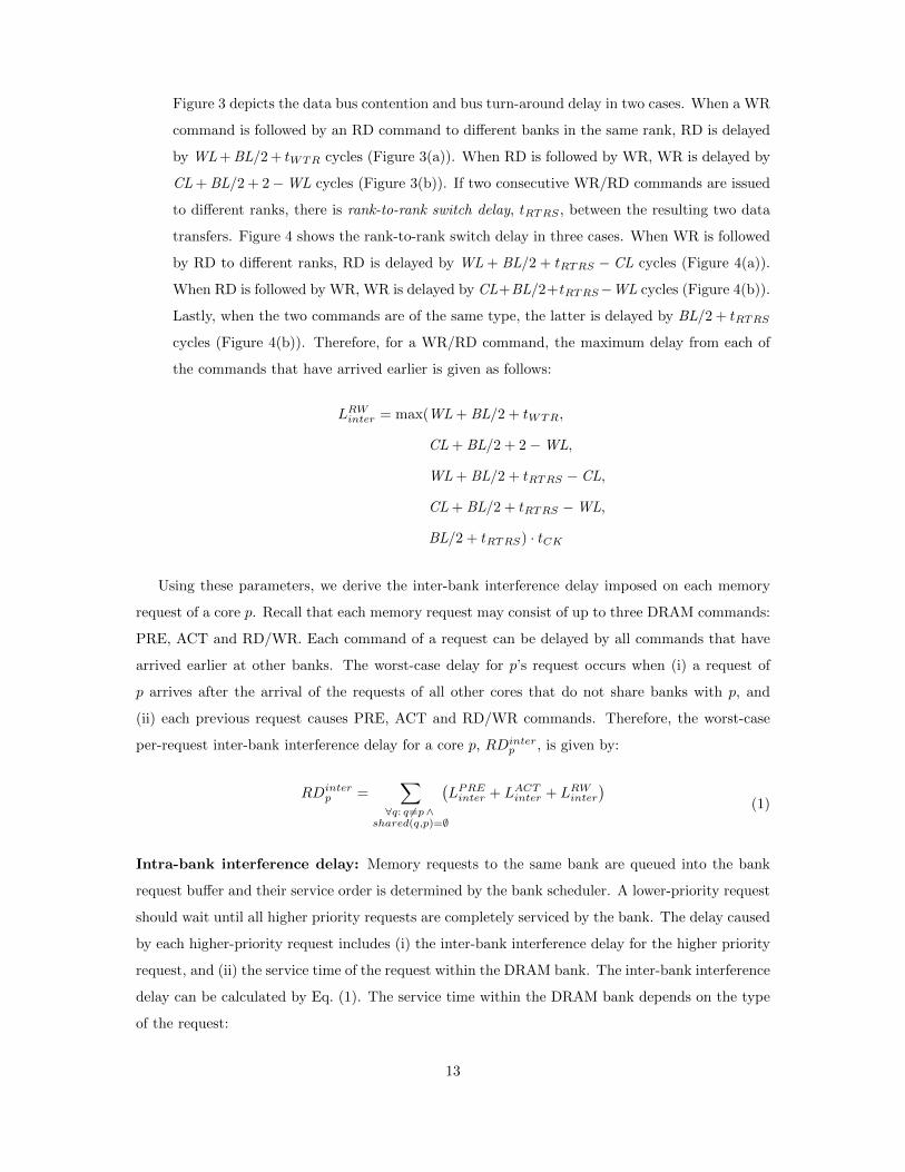
Figure 3 depicts the data bus contention and bus turn-around delay in two cases. When a WR
command is followed by an RD command to different banks in the same rank, RD is delayed
by WL + BL/2 + tWTR cycles (Figure 3(a)). When RD is followed by WR, WR is delayed by
CL + BL/2 + 2−WL cycles (Figure 3(b)). If two consecutive WR/RD commands are issued
to different ranks, there is rank-to-rank switch delay, tRTRS , between the resulting two data
transfers. Figure 4 shows the rank-to-rank switch delay in three cases. When WR is followed
by RD to different ranks, RD is delayed by WL + BL/2 + tRTRS − CL cycles (Figure 4(a)).
When RD is followed by WR, WR is delayed by CL+BL/2+tRTRS−WL cycles (Figure 4(b)).
Lastly, when the two commands are of the same type, the latter is delayed by BL/2 + tRTRS
cycles (Figure 4(b)). Therefore, for a WR/RD command, the maximum delay from each of
the commands that have arrived earlier is given as follows:
LRWinter = max(WL + BL/2 + tWTR,
CL + BL/2 + 2−WL,
WL + BL/2 + tRTRS − CL,
CL + BL/2 + tRTRS −WL,
BL/2 + tRTRS) · tCK
Using these parameters, we derive the inter-bank interference delay imposed on each memory
request of a core p. Recall that each memory request may consist of up to three DRAM commands:
PRE, ACT and RD/WR. Each command of a request can be delayed by all commands that have
arrived earlier at other banks. The worst-case delay for p’s request occurs when (i) a request of
p arrives after the arrival of the requests of all other cores that do not share banks with p, and
(ii) each previous request causes PRE, ACT and RD/WR commands. Therefore, the worst-case
per-request inter-bank interference delay for a core p, RDinterp , is given by:
RDinterp =
∑∀q: q 6=p∧
shared(q,p)=∅
(LPREinter + LACTinter + LRWinter
)(1)
Intra-bank interference delay: Memory requests to the same bank are queued into the bank
request buffer and their service order is determined by the bank scheduler. A lower-priority request
should wait until all higher priority requests are completely serviced by the bank. The delay caused
by each higher-priority request includes (i) the inter-bank interference delay for the higher priority
request, and (ii) the service time of the request within the DRAM bank. The inter-bank interference
delay can be calculated by Eq. (1). The service time within the DRAM bank depends on the type
of the request:
13

• Row-hit service time: The row-hit request is for a requested column already in the row-
buffer. Hence, it can simply read/write its column. In case of read, an RD command takes
CL + BL/2 for data transfer and may cause 2 cycles of delay to the next request for data
bus turn-around time [13]. Note that the read-to-precharge delay (tRTP ) does not need to
be explicitly considered here because the worst-case delay of an RD command is larger than
tRTP in DDR3 SDRAM [13] (or Table 1 for DDR3-1333), i.e., tRTP < CL+BL/2+2. In case
of write, a WR command takes WL+BL/2 for data transfer and may cause max(tWTR, tWR)
of delay to the next request for bus turn-around or write recovery time, depending on the
type of the next request. Thus, in the worst case, the service time for one row-hit request is:
Lhit = max{CL + BL/2 + 2,WL + BL/2 + max(tWTR, tWR)} · tCK
• Row-conflict service time: The row-conflict request should open a row before accessing a
column by issuing PRE and ACT commands, which may take up to tRP and tRCD cycles,
respectively. Hence, the worst-case service time for one row-conflict request is represented as
follows:
Lconf = (tRP + tRCD) · tCK + Lhit
If the next request is also row-conflict and issues PRE and ACT commands, constraints on the
active-to-precharge delay (tRAS) and the row-cycle time (tRC , a minimum separation between
two ACTs in the same bank) should be satisfied. The row-conflict service time Lconf satisfies
tRAS because tRCD · tCK + Lhit is larger than tRAS · tCK in DDR3 SDRAM [13] (or Table 1
for DDR3-1333). Lconf also satisfies tRC , because tRC is equal to tRAS + tRP where tRP is
time for the PRE command of the next request to be completed.
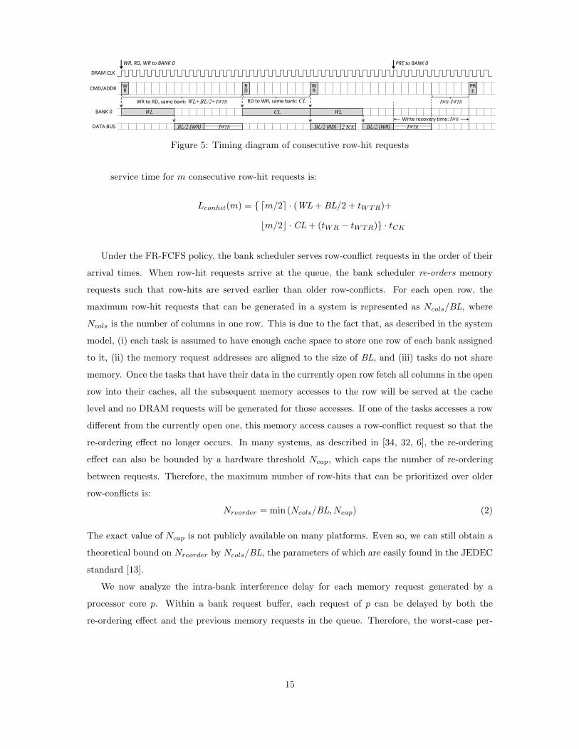
• Consecutive row-hit requests: If m row-hit requests are present in the memory request buffer,
their service time is much smaller than m · Lhit. Due to the data bus turn-around time,
the worst-case service time happens when the requests alternate between read and write, as
depicted in Figure 5. WR followed by RD causes WL+BL/2+ tWTR of delay to RD, and RD
followed by WR causes CL of delay to WR. As WR-to-RD causes larger delay than RD-to-WR
in DDR3 SDRAM [13, 26], m row-hits takes dm2 e · (WL + BL/2 + tWTR) + bm2 c ·CL cycles. In
addition, if a PRE command is the next command to be issued after the m row-hits, it needs
to wait an extra tWR− tWTR cycles due to the write recovery time. Therefore, the worst-case
14
PRE to BANK 0 WR, RD, WR to BANK 0
DRAM CLK
CMD/ADDR R D
BANK 0
W R
DATA BUS BL/2 (WR)
WL
BL/2 (RD)
WR to RD, same bank: WL+BL/2+tWTR
tWTR
CL
W R
WL
2 ·tCK BL/2 (WR) tWTR
RD to WR, same bank: CL
PR E
Write recovery time: tWR
tWR±tWTR
Figure 5: Timing diagram of consecutive row-hit requests
service time for m consecutive row-hit requests is:
Lconhit(m) = { dm/2e · (WL + BL/2 + tWTR)+
bm/2c · CL + (tWR − tWTR)} · tCK
Under the FR-FCFS policy, the bank scheduler serves row-conflict requests in the order of their
arrival times. When row-hit requests arrive at the queue, the bank scheduler re-orders memory
requests such that row-hits are served earlier than older row-conflicts. For each open row, the
maximum row-hit requests that can be generated in a system is represented as Ncols/BL, where
Ncols is the number of columns in one row. This is due to the fact that, as described in the system
model, (i) each task is assumed to have enough cache space to store one row of each bank assigned
to it, (ii) the memory request addresses are aligned to the size of BL, and (iii) tasks do not share
memory. Once the tasks that have their data in the currently open row fetch all columns in the open
row into their caches, all the subsequent memory accesses to the row will be served at the cache
level and no DRAM requests will be generated for those accesses. If one of the tasks accesses a row
different from the currently open one, this memory access causes a row-conflict request so that the
re-ordering effect no longer occurs. In many systems, as described in [34, 32, 6], the re-ordering
effect can also be bounded by a hardware threshold Ncap, which caps the number of re-ordering
between requests. Therefore, the maximum number of row-hits that can be prioritized over older
row-conflicts is:
Nreorder = min (Ncols/BL, Ncap) (2)
The exact value of Ncap is not publicly available on many platforms. Even so, we can still obtain a
theoretical bound on Nreorder by Ncols/BL, the parameters of which are easily found in the JEDEC
standard [13].
We now analyze the intra-bank interference delay for each memory request generated by a
processor core p. Within a bank request buffer, each request of p can be delayed by both the
re-ordering effect and the previous memory requests in the queue. Therefore, the worst-case per-
15
request interference delay for a core p (RDintrap ) is calculated as follows:
RDintrap = reorder(p) +
∑∀q: q 6=p∧
shared(q,p)6=∅
(Lconf +RDinter
q
)(3)
reorder(p) =
0 if @q : q 6= p ∧ shared(q, p) 6= ∅
Lconhit(Nreorder) +
(Nreorder ·
∑∀q: q 6=p∧
shared(q,p)=∅
LRWinter
)+ (tRP + tRCD) · tCK otherwise (4)
In Eq. (3), the summation part calculates the delay from memory requests that can be queued before
the arrival of p’s request. It considers processor cores that share bank partitions with p. Since row-
conflict causes a longer delay than row-hit, the worst-case delay from each of the older requests is
the sum of the row-conflict service time (Lconf ) and the per-request inter-bank interference delay
(RDinterq ). The function reorder(p) calculates the delay from the re-ordering effect. As shown in
Eq. (4), it gives zero if there is no core sharing bank partitions with p. Otherwise, it calculates
the re-ordering effect as the sum of the consecutive row-hits’ service time (Lconhit(Nreorder)) and
the inter-bank delay for the row-hits (Nreorder ·∑LRWinter). In addition, since the memory request
of p that was originally row-hit could become row-conflict due to interfering requests from cores
sharing bank partitions with p, Eq. (4) captures delays for additional PRE and ACT commands
((tRP + tRCD) · tCK).
Total interference delay: A memory request from a core p experiences both inter-bank and
intra-bank interference delay. Hence, the worst-case per-request interference delay for p, RDp, is
represented as follows:
RDp = RDinterp +RDintra
p (5)
Since RDp is the worst-case delay for each request, the total memory interference delay of τi is
upper bounded by Hi ·RDp.
4.2 Job-Driven Bounding Approach
The job-driven approach focuses on how many interfering memory requests are generated during
a task’s job execution time. In the worst case, every memory request from other cores can delay
the execution of a task running on a specific core. Therefore, by capturing the maximum number
of requests generated by the other cores during a time interval t, the job-driven approach bounds
the memory interference delay that can be imposed on tasks running on a specific core in any time
interval t.
We define Ap(t), which is the maximum number of memory requests generated by the core p
16

during a time interval t as:
Ap(t) =∑
∀τi∈task(p)
(⌈t
Ti
⌉+ 1
)·Hi (6)
The “+1” term is to capture the carry-in job of each task during a given time interval t. Note that
this calculation is quite pessimistic, because we do not make assumptions on memory access patterns
(e.g. access rate or distribution). It is possible to add this type of assumptions, such as the specific
memory access pattern of the tasks [9, 5] or using memory request throttling mechanisms [55, 11, 54].
This helps to calculate a tighter Ap(t), while other equations in our work can be used independent
of such additional assumptions.
Inter-bank interference delay: The worst-case inter-bank interference delay imposed on a core
p during a time interval t is represented as follows:
JDinterp (t) =
∑∀q: q 6=p∧
shared(q,p)=∅
Aq(t) ·(LACTinter + LRWinter + LPREinter
)(7)
In this equation, the summation considers processor cores that do not share bank partitions with p.
The other cores sharing banks with p will be taken into account in Eq. (8). The number of memory
requests generated by other cores (Aq(t)) is multiplied by the maximum inter-bank interference
delay from each of these requests (LACTinter + LRWinter + LPREinter).
Intra-bank interference delay: The worst-case intra-bank interference delay imposed on a core
p during t is as follows:
JDintrap (t) =
∑∀q: q 6=p∧
shared(q,p)6=∅
(Aq(t) · Lconf + JDinter
q (t))
(8)
Eq. (8) considers other cores that share bank partitions with p. The number of requests generated
by each of these cores during t is calculated as Aq(t). Since a row-conflict request causes larger
delay than a row-hit one, Aq(t) is multiplied by the row-conflict service time Lconf . In addition,
JDinterq is added because each interfering core q itself may be delayed by inter-bank interference
depending on its bank partitions. Note that the re-ordering effect of the bank scheduler does not
need to be considered here because Eq. (8) captures the worst case where all the possible memory
requests generated by other cores arrived ahead of any request from p.
Total interference delay: The worst-case memory interference delay is the sum of the worst-case
inter-bank and intra-bank delays. Therefore, the memory interference delay for a core p during a
17

time interval t, JDp(t), is upper bounded by:
JDp(t) = JDinterp (t) + JDintra
p (t) (9)
It is worth noting that the job-driven approach will give a tighter bound than the request-driven
approach when the number of interfering memory requests from other cores is relatively small
compared to the number of the memory requests of the task under analysis. Conversely, in the
opposite case, the request-driven approach will give a tighter bound than the job-driven approach.
We will compare the results of these two approaches in Section 6.
4.3 Response-Time Based Schedulability Analysis
We have presented the request-driven and the job-driven approaches to analyze the worst-case
memory interference delay. Since each of the two approaches bounds the interference delay by
itself, a tighter upper bound can be obtained by taking the smaller result from the two approaches.
Based on the analyses of the two approaches, the iterative response time test [16] is extended as
follows to incorporate the memory interference delay:
Rk+1i = Ci +
∑τj∈hp(τi)
⌈RkiTj
⌉· Cj
+ min
Hi ·RDp+∑
τj∈hp(τi)
⌈RkiTj
⌉·Hj ·RDp, JDp(R
ki )
(10)
where Rki is the worst-case response time of τi at the kth iteration, and p is proc(τi). The test
terminates when Rk+1i = Rki . The task τi is schedulable if its response time does not exceed its
deadline: Rki ≤ Di. The first and the second terms are the same as the classical response time test.
In the third term, the memory interference delay for τi is bounded by using the two approaches. The
request-driven approach bounds the delay with the addition of of Hi ·RDp and∑dR
ki
Tje ·Hj ·RDp,
which is the total delay imposed on τi and its higher priority tasks. The job-driven approach bounds
the delay by JDp(Rki ), that captures the total delay incurred during τi’s response time.
4.4 Memory Controllers with Write Batching
Many recent memory controllers handle write requests in batches when the write buffer is close to
full so that the bus turn-around delay can be amortized across many requests [26, 57]. Although
the modeling of memory controllers using write batching is not within the scope of our work, we
believe that our analysis could still be used to bound memory interference in systems with such
memory controllers. If a memory controller uses write batching, the worst-case delay of a single
18

memory operation can be much larger than the one computed by LPREinter + LACTinter + LRWinter, due
to write-buffer draining.7 However, this does not restrict the applicability of our theory on such
memory controllers. We discuss this from two cases as follows.
First, consider a job of task τi and how it experiences interference from a job of task τj where τj
is assigned to a different core than τi. If the job of τi starts its execution at a time when the write
buffer is fully filled with the memory requests of the job of τj , then the job of τi suffers additional
interference from at most w memory requests, where w is the size of the write buffer. However, this
effect can only happen once per the job of τi and be bounded by a constant value. Afterwards, the
total number of interfering memory requests remains the same during the execution of the job of
τi. In addition, since the use of write batching reduces memory bus turn-around delay, it may even
shorten the response time of the job of τi.
Second, consider a job of task τi and how it experiences interference from a job of task τj where
τj is assigned to the same core as τi. If the job of τi starts its execution at a time when the write
buffer is full with the memory requests of the job of τj , all the memory requests in the write buffer
need to be serviced first, which can delay the execution of the job of τi. However, this effect can
only happen once per context switch and hence it can be accounted for as a preemption cost.
5 Reducing Memory Interference via Task Allocation
In this section, we present our memory interference-aware task allocation algorithm to reduce
memory interference during the allocation phase. Our algorithm is motivated by the following
observations we have made from our analysis given in Section 4: (i) memory interference for a
task is caused by other tasks running on other cores in parallel, (ii) tasks running on the same
core do not interfere with each other, and (iii) the use of bank partitioning reduces the memory
interference delay. These observations lead to an efficient task allocation under partitioned schedul-
ing. By co-locating memory-intensive tasks on the same core with dedicated DRAM banks, the
amount of memory interference among tasks can be significantly reduced, thereby providing better
schedulability.
Our memory interference-aware allocation algorithm (MIAA) is given in Algorithm 1. MIAA
takes three input parameters: Γ is a set of tasks to be allocated, NP is the number of available
processor cores, and NBP is the number of available bank partitions. MIAA returns schedulable, if
every task in Γ can meet its deadline, and unschedulable, if any task misses its deadline.
7Note that the write-buffer draining does not completely block read requests until all the write requests areserviced. In a memory controller with write batching, read requests are always exposed to the memory controller,but write requests are exposed to and scheduled by the memory controller only when the write buffer is close tofull [26]. Hence, even when the write buffer is being drained, a read request can be scheduled if its commands areready with respect to DRAM timing constraints (e.g., read and write requests to different banks).
19

Algorithm 1 MIAA(Γ, NP , NBP )
Input: Γ: a taskset to be allocated, NP : the number of processor cores, NBP : the number of available bankpartitions
Output: Schedulability of Γ1: G← MemoryInterferenceGraph(Γ)2: task(p1)← ∅3: bank(p1)← LeastInterferingBank(NBP ,P,G,Γ)4: P← {p1}5: Φ← {Γ}6: while Φ 6= ∅ do7: /* Allocates bundles */8: Φ′ ← Φ; Φrest ← ∅9: for all ϕi ∈ Φ′ in descending order of utilization do
10: Φ← Φ \ {ϕi}11: pbestfit ← BestFit(ϕi,P)12: if pbestfit 6= invalid then13: for all pj ∈ P : pj 6= pbestfit ∧ ¬schedulable(pj) do14: Φ← Φ ∪ {RemoveExcess(pj ,G)}15: else16: Φrest ← Φrest ∪ {ϕi}17: if |Φrest| = 0 then18: continue19: /* Breaks unallocated bundles */20: all singletons← true21: for all ϕi ∈ Φrest do22: if |ϕi| > 1 then23: all singletons← false24: pemptiest ← argmin
pi∈P(utilization(pi))
25: (ϕj , ϕk)←ExtractMinCut(ϕi, 1− utilization(pemptiest),G)26: Φ← Φ ∪ {ϕj , ϕk}27: else28: Φ← Φ ∪ {ϕi}29: /* Opens a new processor core */30: if all singletons = true then31: if |P| = NP then32: return unschedulable33: ϕ←
⋃ϕi∈Φ
ϕi
34: task(pnew)← ∅35: bank(pnew)←LeastInterferingBank(NBP ,P,G, ϕ)36: P← P ∪ {pnew}37: Φ← {ϕ}38: return schedulable
To understand the intensity of memory interference among tasks, MIAA first constructs a mem-
ory interference graph G (line 1 of Alg. 1). The graph G is a fully-connected, weighted, undirected
graph, where each node represents a task and the weight of an edge between two nodes represents
the amount of memory interference that the corresponding two tasks can generate. Algorithm 2
gives the pseudo-code for constructing G. For each pair of two tasks, τi and τj , the edge weight
between the two tasks is calculated as follows. First, the two tasks are assumed to be assigned to
two empty cores that share the same bank partition. Then, the response times of the two tasks,
Ri and Rj , are calculated by using Eq. (10), assuming that no other tasks are executing in the
system. Since each task is the only task allocated to its core, the task response time is equal to
the sum of the task WCET and the memory interference delay imposed on the task. Hence, we use
(Ri −Ci)/Ti + (Rj −Cj)/Tj as the edge weight between τi and τj (weight(G, τi, τj)), which repre-
20

Algorithm 2 MemoryInterferenceGraph(Γ)
Input: Γ: a taskset (Γ = {τ1, τ2, ..., τn})Output: G: a graph with tasks as nodes and memory interference-intensity among nodes as edge weights1: Construct a fully-connected undirected graph G with tasks in Γ as nodes2: for i← 1 to n do3: for j ← i+ 1 to n do4: Let two processors, p1 and p2, share the same bank partition5: task(p1)← {τi}6: task(p2)← {τj}7: Ri ← response time of τi8: Rj ← response time of τj9: weight(G, τi, τj)← (Ri − Ci)/Ti + (Rj − Cj)/Tj
10: return G
Algorithm 3 LeastInterferingBank(NBP ,P,G, ϕ)
Input: NBP : the number of bank partitions, P: a set of processor cores, G: a memory interference graph, ϕ: a setof tasks that have not been allocated to cores yet
Output: b: a bank partition index (1 ≤ b ≤ NBP )1: if |P| < NBP then2: return indexof(unused bank partition())3: pmin ← p1
4: wpmin ←∞5: for all pi ∈ P do6: wpi ←
∑τj∈task(pi)
∑τk∈ϕ weight(G, τj , τk)
7: if wpmin > wpi then8: pmin ← pi9: wpmin ← wpi
10: return bank(pmin)
sents the amount of CPU utilization penalty that may occur due to memory interference among τi
and τj .
After constructing the graph G, MIAA opens one core, p1, by adding it to the core set P.
It is worth noting that every time a new core is opened (added to P), a bank partition is as-
signed to it by the LeastInterferingBank() function given in Algorithm 3. The purpose of
LeastInterferingBank() is to find a bank partition that likely leads to the least amount of memory
interference to the tasks that have not been allocated yet (input parameter ϕ of Alg. 3). If the num-
ber of cores in P does not exceed the number of bank partitions (NBP ), LeastInterferingBank()
returns the index of an unused bank partition (line 2 of Alg. 3). Otherwise, LeastInterferingBank()
tries to find the least interfering bank by using G as follows. For each core pi, it calculates wpi that
is the sum of the weights of all edges between the tasks in pi and the tasks in ϕ. Then, it returns
the bank partition index of a core pmin with the smallest wpmin.
The allocation strategy of MIAA is to group memory-intensive tasks into a single bundle and
allocate as many tasks in each bundle as possible into the same core. To do so, MIAA first groups
all tasks in Γ into a single bundle and assign that bundle as an element of the set of bundles to be
allocated (line 5 of Alg. 1). Then, it allocates all bundles in Φ based on the best-fit decreasing (BFD)
heuristic (from line 9 to line 16). Here, we define the utilization of a bundle ϕi as∑τk∈ϕk
Ck/Tk.
Bundles are sorted in descending order of utilization and MIAA tries to allocate each bundle to a
21

Algorithm 4 BestFit(ϕ,P)
Input: ϕ: a task bundle to be allocated, P: a set of available processor coresOutput: pi: the processor core where ϕ is allocated (pi = invalid, if the allocation fails)1: for all pi ∈ P in non-increasing order of utilization do2: task(pi)← task(pi) ∪ ϕ3: if schedulable(pi) then4: return pi5: task(pi)← task(pi) \ ϕ6: return invalid
Algorithm 5 RemoveExcess(pi,G)
Input: pi: a processor core, G: a memory interference graphOutput: ϕ: a set of tasks removed from pi1: ϕ← ∅2: repeat3: wτmin ←∞4: for all τj ∈ task(pi) do5: wτi ←
∑τk∈task(pi)∧τk 6=τj weight(G, τj , τk)
6: if wτmin > wτi then7: τmin ← τj8: wτmin ← wτi9: task(pi)← task(pi) \ {τmin}
10: ϕ← ϕ ∪ {τmin}11: until schedulable(pi)12: return ϕ
core by using the BestFit() function given in Algorithm 4. This algorithm finds the best-fit core
that can schedule a given bundle with the least amount of remaining utilization. The utilization of
a core pi is defined as∑τk∈task(pi) Ck/Tk. If a bundle is allocated (line 12 of Alg. 1), that bundle
may introduce additional memory interference to all other cores. Therefore, we need to check if
the other cores can still schedule their tasksets. If any core becomes unschedulable due to the
just-allocated bundle, MIAA uses the RemoveExcess() function to remove enough tasks from the
core in order to make it schedulable again, and puts the removed tasks as a new bundle into Φ
(line 14). Conversely, if a bundle is not allocated to any core (line 15), it is put into Φrest and will
be considered later.
We shall explain the RemoveExcess() function before moving onto the next phase of MIAA.
The pseudo-code of RemoveExcess() is given in Algorithm 5. The goal of this function is to make
the core pi schedulable again while keeping as many memory-intensive tasks as possible. To do so,
the function extracts one task at a time from the core with the following two steps. In step one, it
calculates the weight wτi for each task τi, which is the sum of all edge weights from τi to the other
tasks on the same core. In step two, it removes a task τmin with the smallest wτminfrom the core.
These two steps are repeated until the core becomes schedulable. Then, the function groups the
removed tasks into a single bundle and returns it.
Once the bundle allocation phase is done, MIAA attempts to break unallocated bundles in Φrest
(line 21 of Alg. 1). If an unallocated bundle ϕi contains more than one task, it is broken into two
sub-bundles by the ExtractMinCut() function such that the utilization of the first sub-bundle does
22
Algorithm 6 ExtractMinCut(ϕ,max util,G)
Input: ϕ: a task bundle to be broken, max util: the maximum utilization allowed for the first sub-bundle, G: amemory interference graph
Output: (ϕ′, ϕ′′): a tuple of sub-bundles1: Find a task τi ∈ ϕ with the highest utilization2: ϕ′ ← {τi}3: ϕ′′ ← ϕ \ {τi}4: while |ϕ′′| > 1 do5: wτmax ← −16: for all τi ∈ ϕ′′ do7: w ←
∑τj∈ϕ′ weight(G, τi, τj)
8: if wτmax < w then9: τmax ← τi
10: wτmax ← w11: if utilization(ϕ′ ∪ {τmax}) ≤ max util then12: ϕ′ ← ϕ′ ∪ {τmax}13: ϕ′′ ← ϕ′′ \ {τmax}14: else15: break16: return (ϕ′, ϕ′′)
not exceed the remaining utilization of the emptiest core (line 25). If ϕi has only one task in it, ϕi is
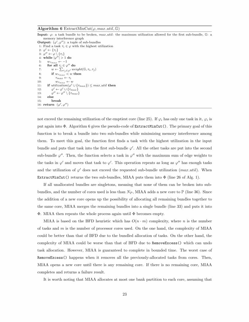
put again into Φ. Algorithm 6 gives the pseudo-code of ExtractMinCut(). The primary goal of this
function is to break a bundle into two sub-bundles while minimizing memory interference among
them. To meet this goal, the function first finds a task with the highest utilization in the input
bundle and puts that task into the first sub-bundle ϕ′. All the other tasks are put into the second
sub-bundle ϕ′′. Then, the function selects a task in ϕ′′ with the maximum sum of edge weights to
the tasks in ϕ′ and moves that task to ϕ′. This operation repeats as long as ϕ′′ has enough tasks
and the utilization of ϕ′ does not exceed the requested sub-bundle utilization (max util). When
ExtractMinCut() returns the two sub-bundles, MIAA puts them into Φ (line 26 of Alg. 1).
If all unallocated bundles are singletons, meaning that none of them can be broken into sub-
bundles, and the number of cores used is less than NP , MIAA adds a new core to P (line 36). Since
the addition of a new core opens up the possibility of allocating all remaining bundles together to
the same core, MIAA merges the remaining bundles into a single bundle (line 33) and puts it into
Φ. MIAA then repeats the whole process again until Φ becomes empty.
MIAA is based on the BFD heuristic which has O(n · m) complexity, where n is the number
of tasks and m is the number of processor cores used. On the one hand, the complexity of MIAA
could be better than that of BFD due to the bundled allocation of tasks. On the other hand, the
complexity of MIAA could be worse than that of BFD due to RemoveExcess() which can undo
task allocation. However, MIAA is guaranteed to complete in bounded time. The worst case of
RemoveExcess() happens when it removes all the previously-allocated tasks from cores. Then,
MIAA opens a new core until there is any remaining core. If there is no remaining core, MIAA
completes and returns a failure result.
It is worth noting that MIAA allocates at most one bank partition to each core, assuming that
23

one bank partition is sufficient to meet the memory requirements of any set of tasks that may be
allocated to a single core. This assumption can be satisfied by configuring one bank partition to have
multiple DRAM banks, as discussed in Section 2.3. However, we believe that explicitly modeling
each task’s memory requirement can help in providing better schedulability, which remains as our
future work.
6 Evaluation
In this section, we first compare the memory interference delay observed in a real platform with
the one predicted by our analysis. Then, we evaluate our memory interference-aware allocation
algorithm.
6.1 Memory Interference in a Real Platform
6.1.1 Experimental Setup
The target platform is equipped with an Intel Core i7-2600 quad-core processor running at 3.4 GHz.
The on-chip memory controller of the processor supports dual memory channels, but by installing
a single DIMM, only one channel is activated in accordance with our system model.8 The platform
uses a single DDR3-1333 DIMM that consists of 2 ranks and 8 banks per each rank. The timing
parameters of the DIMM are shown in Table 1.
We used the latest version of Linux/RK [37, 41] for software cache and bank partitioning [18,
48].9 Cache partitioning divides the shared L3 cache of the processor into 32 partitions, and bank
partitioning divides the DRAM banks into 16 partitions (1 DRAM bank per partition). For the mea-
surement tool, we used the Linux/RK profiler [19] that records execution times and memory accesses
(LLC misses) using hardware performance counters. In addition, we used the memory reservation
mechanism of Linux/RK [12, 20] to protect each application against unexpected page swap-outs.
To reduce measurement inaccuracies and improve predictability, we disabled the stride-based and
adjacent cache-line prefetchers, simultaneous multithreading, and dynamic clock frequency scaling
of the processor. All unrelated system services such as GUI and networking were also disabled.
It is worth noting that some of our assumptions do not hold in the target platform. First, the
processor of the target platform is not fully timing-compositional, in that it can generate multiple
outstanding memory requests and hide memory access delay by out-of-order execution. Second, the
memory controller of the target platform uses write batching, and there may be other discordances
between the memory controller and our system model because detailed information on the memory
8This is why the DRAM address mapping in Figure 1(c) does not have a bit for channel selection.9Linux/RK is available at https://rtml.ece.cmu.edu/redmine/projects/rk.
24
controller is not open to the public. However, we have chosen the target platform because (i) it is
equipped with DDR3 SDRAM which is our main focus in this work, and (ii) it can run an OS that
provides the software cache and DRAM bank partitioning features needed for our experiments. We
will explore how the aforementioned differences between the target platform and our system model
influences our experimental results.
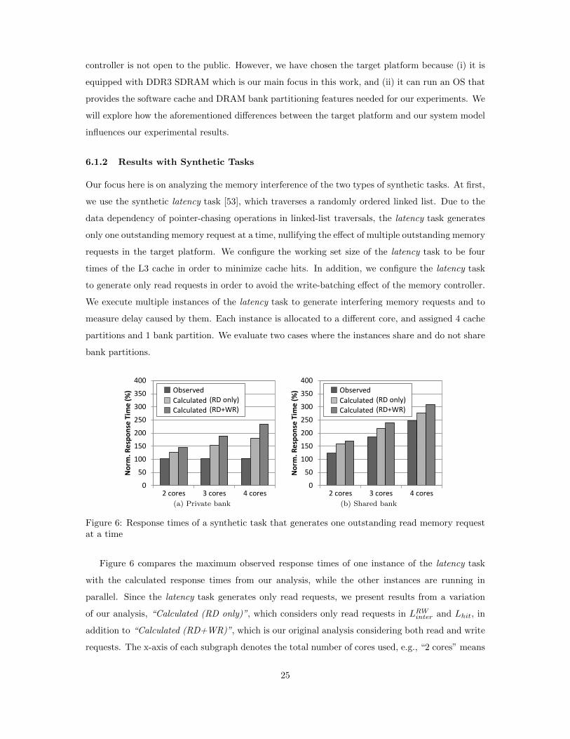
6.1.2 Results with Synthetic Tasks
Our focus here is on analyzing the memory interference of the two types of synthetic tasks. At first,
we use the synthetic latency task [53], which traverses a randomly ordered linked list. Due to the
data dependency of pointer-chasing operations in linked-list traversals, the latency task generates
only one outstanding memory request at a time, nullifying the effect of multiple outstanding memory
requests in the target platform. We configure the working set size of the latency task to be four
times of the L3 cache in order to minimize cache hits. In addition, we configure the latency task
to generate only read requests in order to avoid the write-batching effect of the memory controller.
We execute multiple instances of the latency task to generate interfering memory requests and to
measure delay caused by them. Each instance is allocated to a different core, and assigned 4 cache
partitions and 1 bank partition. We evaluate two cases where the instances share and do not share
bank partitions.
0
50
100
150
200
250
300
350
400
2 cores 3 cores 4 cores
No
rm.
Re
spo
nse
Tim
e (
%) Observed
Calculated (RD+WR)
Calculated (RD only)
(a) Private bank
0
50
100
150
200
250
300
350
400
2 cores 3 cores 4 cores
No
rm.
Re
spo
nse
Tim
e (
%) Observed
Calculated (RD+WR)
Calculated (RD only)
(b) Shared bank
Figure 6: Response times of a synthetic task that generates one outstanding read memory requestat a time
Figure 6 compares the maximum observed response times of one instance of the latency task
with the calculated response times from our analysis, while the other instances are running in
parallel. Since the latency task generates only read requests, we present results from a variation
of our analysis, “Calculated (RD only)”, which considers only read requests in LRWinter and Lhit, in
addition to “Calculated (RD+WR)”, which is our original analysis considering both read and write
requests. The x-axis of each subgraph denotes the total number of cores used, e.g., “2 cores” means
25

that two instances run on two different cores and the other cores are left idle. The y-axis shows
the response time of the instance under analysis, normalized to the case when it runs alone in the
system. Since each instance is allocated alone to each core, the response time increase is equal to
the amount of memory interference suffered from other cores. The difference between the observed
and calculated values represents the pessimism embedded in our analysis. Figure 6(a) shows the
response times when each instance has a private bank partition. We observed a very small increase
in response times even when all four cores were used. This is because (i) each instance of the
latency task does not experience intra-bank interference due to its private bank partition, and (ii)
each instance generates a relatively small number of memory requests, so each memory request is
likely serviced before the arrival of requests from other cores. However, our analysis pessimistically
assumes that each memory request may always be delayed by the memory requests of all other
cores. In addition, the executions of DRAM commands at different banks can be overlapped as
long as DRAM timing constraints are not violated, but our analysis does not consider such an
overlapping effect.
Figure 6(b) depicts the response times when all cores share the same bank partition. We set
the re-ordering window size Nreorder to zero in our analysis, because the latency task accesses a
randomly ordered linked list and has very low row-buffer locality, thereby hardly generating row-hit
requests. As can be seen in this figure, the results from both of our analyses bound the observed
response times. The pessimism of our analysis in the shared bank case is not as significant as
the one in the private bank case. This is due to the fact that the use of a single shared bank
serializes the executions of DRAM commands from multiple cores, making their executions close to
the worst-case considered by our analysis.
0
100
200
300
400
500
600
700
800
900
1000
2 cores 3 cores 4 cores
No
rm.
Re
spo
nse
Tim
e (
%) Observed
Calculated
(a) Private bank
0
100
200
300
400
500
600
700
800
900
1000
2 cores 3 cores 4 cores
No
rm.
Re
spo
nse
Tim
e (
%) Observed
Calculated (Nreorder = 0)
(b) Shared bank
Figure 7: Response times of a synthetic task that generates multiple outstanding read and writememory requests at a time
Next, we use a synthetic memory-intensive task which has the opposite characteristics of the
latency task. The memory-intensive task is a modified version of the stream benchmark [31]. The
26

memory-intensive task generates a combination of read and write requests with very high row-buffer
locality and little computation. In addition, it can generate multiple outstanding memory requests
in the target platform due to the lack of data dependency. Therefore, by using the memory-intensive
task, we can identify the effects of the differences between the target platform and our analysis.
Similar to the latency task experiments, we execute multiple instances of the memory-intensive
task, with each assigned 4 cache partitions and 1 bank partition, and compare private and shared
bank cases.
Figure 7 compares the response times of one instance of the memory-intensive task, while the
other instances are running in parallel. Since the memory-intensive task generates both read and
write requests, we do not consider our read-only analysis used in Figure 6. Figure 7(a) shows the
response times with a private bank partition per core. Since the memory-intensive task generates a
larger number of memory requests than the latency task, the observed response times of the memory-
intensive task is longer than the ones of the latency task. Interestingly, although the memory-
intensive task might generate multiple outstanding memory requests at a time, our analysis could
bound memory interference delay. This is because the extra penalty caused by multiple outstanding
memory requests can be compensated by various latency-hiding effects in the target platform. First,
an increase in the memory access latency can be hidden by the out-of-order execution of the target
processor. Second, the memory controller handles the write requests in batches, which can reduce
the processor stall time. However, in order to precisely analyze memory interference in a platform
like ours, both the extra penalty caused by multiple outstanding memory requests and the latency-
hiding effects from out-of-order execution and write batching should be accounted for by analysis,
which remains as future work.
Figure 7(b) illustrates the response times when all cores share the same bank partition. Since
the memory-intensive task has very high row-buffer locality, we expected that a large re-ordering
window size Nreorder would be needed for our analysis to bound the re-ordering effect. However,
as shown in this figure, our analysis could bound memory interference even when we set Nreorder
to zero. We suspect that the re-ordering effect on the memory-intensive task is canceled out by the
memory latency-hiding techniques of the target platform.
6.1.3 Results with PARSEC Benchmarks
We now analyze the memory interference delay of the PARSEC benchmarks [8], which are closer
to the memory access patterns of real applications compared to the synthetic tasks used in Sec-
tion 6.1.2. A total of eleven PARSEC benchmarks are used in this experiment. Two PARSEC
benchmarks, dedup and facesim, are excluded from the experiment due to their frequent disk ac-
cesses for data files. In order to compare the impact of different amounts of interfering memory
27
requests, we use the two types of synthetic tasks, memory-intensive and memory-non-intensive.
Each PARSEC benchmark is assigned to Core 1 and the synthetic tasks are assigned to the other
cores (Core 2, 3, 4) to generate interfering memory requests. To meet the memory size requirement
of the benchmarks, each benchmark is assigned 20 private cache partitions.10 The synthetic tasks
are each assigned 4 private cache partitions. Each of the benchmarks and the synthetic tasks is
assigned 1 bank partition, and we evaluate two cases where tasks share or do not share bank par-
titions. The memory-intensive task is the one used in Section 6.1.2. When running in isolation,
the memory-intensive task generates up to 40K DRAM requests per msec (combination of read
and write). Since it has very high row-buffer locality with little computations, “40K requests per
msec” is likely close to the maximum possible value that a single core can generate with a single
bank partition in the target system. The memory-non-intensive task has a similar structure to
the stream benchmark [31], but it has multiple non-memory operations between memory opera-
tions, thereby generating much fewer DRAM requests. When running alone in the system, the
memory-non-intensive task generates up to 1K DRAM requests per msec.
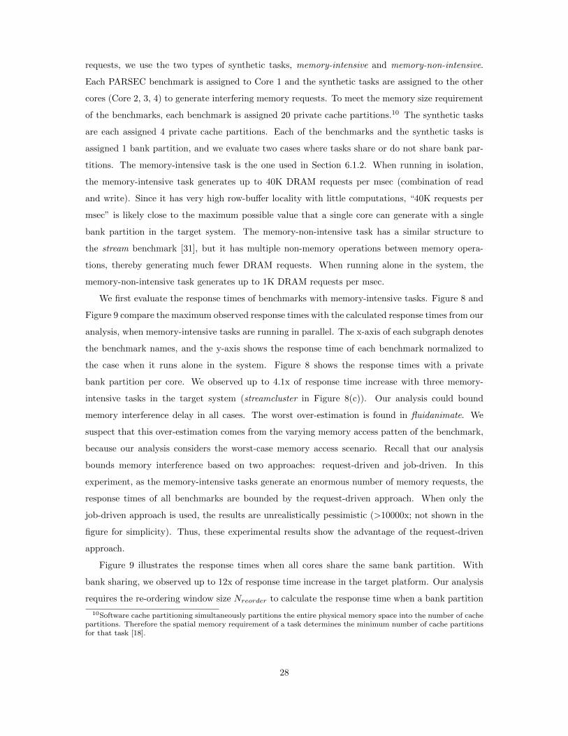
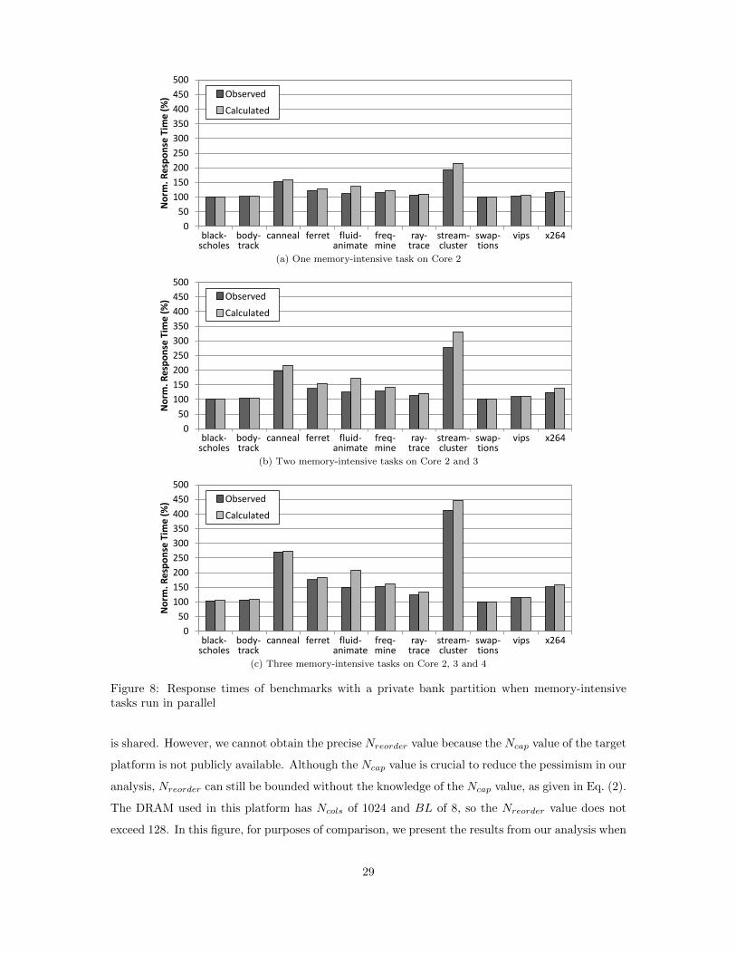
We first evaluate the response times of benchmarks with memory-intensive tasks. Figure 8 and
Figure 9 compare the maximum observed response times with the calculated response times from our
analysis, when memory-intensive tasks are running in parallel. The x-axis of each subgraph denotes
the benchmark names, and the y-axis shows the response time of each benchmark normalized to
the case when it runs alone in the system. Figure 8 shows the response times with a private
bank partition per core. We observed up to 4.1x of response time increase with three memory-
intensive tasks in the target system (streamcluster in Figure 8(c)). Our analysis could bound
memory interference delay in all cases. The worst over-estimation is found in fluidanimate. We
suspect that this over-estimation comes from the varying memory access patten of the benchmark,
because our analysis considers the worst-case memory access scenario. Recall that our analysis
bounds memory interference based on two approaches: request-driven and job-driven. In this
experiment, as the memory-intensive tasks generate an enormous number of memory requests, the
response times of all benchmarks are bounded by the request-driven approach. When only the
job-driven approach is used, the results are unrealistically pessimistic (>10000x; not shown in the
figure for simplicity). Thus, these experimental results show the advantage of the request-driven
approach.
Figure 9 illustrates the response times when all cores share the same bank partition. With
bank sharing, we observed up to 12x of response time increase in the target platform. Our analysis
requires the re-ordering window size Nreorder to calculate the response time when a bank partition
10Software cache partitioning simultaneously partitions the entire physical memory space into the number of cachepartitions. Therefore the spatial memory requirement of a task determines the minimum number of cache partitionsfor that task [18].
28
0
50
100
150
200
250
300
350
400
450
500
No
rm.
Re
spo
nse
Tim
e (
%) Observed
Calculated
black- scholes
body- track
canneal ferret fluid- animate
freq- mine
ray- trace
stream- cluster
swap- tions
vips x264
(a) One memory-intensive task on Core 2
0
50
100
150
200
250
300
350
400
450
500
No
rm.
Re
spo
nse
Tim
e (
%) Observed
Calculated
black- scholes
body- track
canneal ferret fluid- animate
freq- mine
ray- trace
stream- cluster
swap- tions
vips x264
(b) Two memory-intensive tasks on Core 2 and 3
0
50
100
150
200
250
300
350
400
450
500
No
rm.
Re
spo
nse
Tim
e (
%) Observed
Calculated
black- scholes
body- track
canneal ferret fluid- animate
freq- mine
ray- trace
stream- cluster
swap- tions
vips x264
(c) Three memory-intensive tasks on Core 2, 3 and 4
Figure 8: Response times of benchmarks with a private bank partition when memory-intensivetasks run in parallel
is shared. However, we cannot obtain the precise Nreorder value because the Ncap value of the target
platform is not publicly available. Although the Ncap value is crucial to reduce the pessimism in our
analysis, Nreorder can still be bounded without the knowledge of the Ncap value, as given in Eq. (2).
The DRAM used in this platform has Ncols of 1024 and BL of 8, so the Nreorder value does not
exceed 128. In this figure, for purposes of comparison, we present the results from our analysis when
29

0
200
400
600
800
1000
1200
1400
1600
No
rm.
Re
spo
nse
Tim
e (
%)
black- scholes
body- track
canneal ferret fluid- animate
freq- mine
ray- trace
stream- cluster
swap- tions
vips x264
Observed
Calculated
Calculated
(Nreorder = 0)
(Nreorder = 12)
Calculated (Nreorder = 6)
(a) One memory-intensive task on Core 2
0
200
400
600
800
1000
1200
1400
1600
No
rm.
Re
spo
nse
Tim
e (
%)
black- scholes
body- track
canneal ferret fluid- animate
freq- mine
ray- trace
stream- cluster
swap- tions
vips x264
Observed
Calculated
Calculated
(Nreorder = 0)
(Nreorder = 12)
Calculated (Nreorder = 6)
(b) Two memory-intensive tasks on Core 2 and 3
0
200
400
600
800
1000
1200
1400
1600
No
rm.
Re
spo
nse
Tim
e (
%)
black- scholes
body- track
canneal ferret fluid- animate
freq- mine
ray- trace
stream- cluster
swap- tions
vips x264
Observed
Calculated
Calculated
(Nreorder = 0)
(Nreorder = 12)
Calculated (Nreorder = 6)
(c) Three memory-intensive tasks on Core 2, 3 and 4
Figure 9: Response times of benchmarks with a shared bank partition when memory-intensive tasksrun in parallel
Nreorder is set to 0, 6, and 12. If we disregard the re-ordering effect of FR-FCFS in this platform
(Nreorder = 0), the analysis generates overly optimistic values. In case of streamcluster with three
memory-intensive tasks (Figure 9(c)), the analysis that does not account for the re-ordering effect
results in only about half of the observed one. When Nreorder = 12, our analysis can find bounds in
all cases. However, this does not necessarily mean that the re-ordering window size of the memory
30
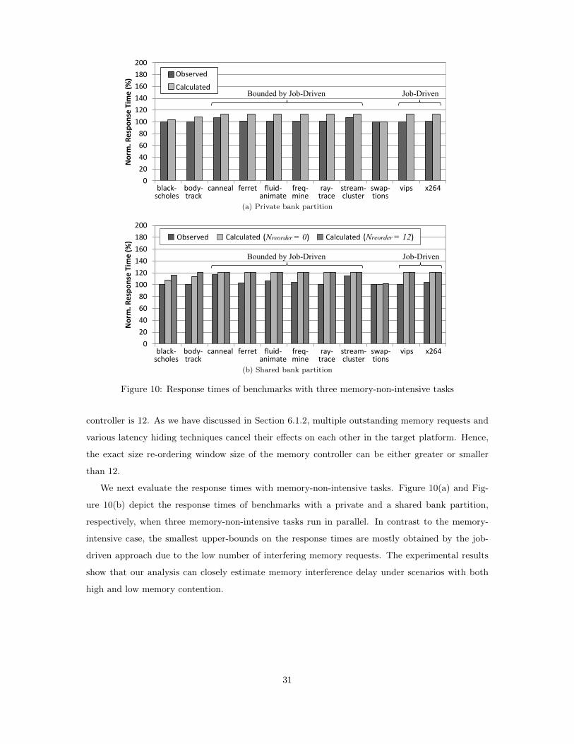
0
20
40
60
80
100
120
140
160
180
200
No
rm.
Re
spo
nse
Tim
e (
%)
Observed
CalculatedBounded by Job-Driven Job-Driven
black- scholes
body- track
canneal ferret fluid- animate
freq- mine
ray- trace
stream- cluster
swap- tions
vips x264
(a) Private bank partition
0
20
40
60
80
100
120
140
160
180
200
No
rm.
Re
spo
nse
Tim
e (
%)
Observed Calculated (Nreorder = 0) Calculated (Nreorder = 12)
Bounded by Job-Driven Job-Driven
black- scholes
body- track
canneal ferret fluid- animate
freq- mine
ray- trace
stream- cluster
swap- tions
vips x264
(b) Shared bank partition
Figure 10: Response times of benchmarks with three memory-non-intensive tasks
controller is 12. As we have discussed in Section 6.1.2, multiple outstanding memory requests and
various latency hiding techniques cancel their effects on each other in the target platform. Hence,
the exact size re-ordering window size of the memory controller can be either greater or smaller
than 12.
We next evaluate the response times with memory-non-intensive tasks. Figure 10(a) and Fig-
ure 10(b) depict the response times of benchmarks with a private and a shared bank partition,
respectively, when three memory-non-intensive tasks run in parallel. In contrast to the memory-
intensive case, the smallest upper-bounds on the response times are mostly obtained by the job-
driven approach due to the low number of interfering memory requests. The experimental results
show that our analysis can closely estimate memory interference delay under scenarios with both
high and low memory contention.
31

Table 2: Base parameters for allocation algorithm experiments
Parameters ValuesNumber of processor cores (NP ) 8Number of bank partitions (NBP ) 8Number of tasks to be allocated 20Task period (Ti) uniform from [100, 200] msecTask utilization (Ui) uniform from [0.1, 0.3]Task WCET (Ci) Ui · TiTask deadline (Di) equal to TiRatio of memory-intensive tasks to memory-non-intensive tasks 5:5Hi for memory-intensive task uniform from [10000, 100000]Hi for memory-non-intensive task uniform from [100, 1000]
6.2 Memory Interference-Aware Task Allocation
In this subsection, we evaluate the effectiveness of our memory interference-aware allocation (MIAA)
algorithm. To do this, we use randomly-generated tasksets and capture the percentage of schedu-
lable tasksets as the metric.
6.2.1 Experimental Setup
The base parameters we use for experiments are summarized in Table 2. Once a taskset is generated,
the priorities of tasks are assigned by the Rate Monotonic Scheduling (RMS) policy [28]. The
same DRAM parameters as in Table 1 are used, and the re-ordering window size of 12 is used
(Nreorder = 12).
We consider the following six schemes for performance comparison: (i) the best-fit decreasing
algorithm (BFDnB), (ii) BFD with bank partitioning (BFDwB), (iii) the first-fit decreasing algo-
rithm (FFDnB), (iv) FFD with bank partitioning (FFDwB), (v) the IA3 algorithm proposed in
[38] (IA3nB), and (vi) IA3 with bank partitioning (IA3wB). The BFD and FFD algorithms are
traditional bin-packing heuristics, and IA3 is a recent interference-aware task allocation algorithm
based on FFD. As none of these algorithms is originally designed to consider bank partitioning,
all cores share all available bank partitions under BFDnB, FFDnB and IA3nB. Conversely, under
BFDwB, FFDwB and IA3wB, bank partitions are assigned to cores in round-robin order so that
each core can have a dedicated bank partition. In all these algorithms, we use our response-time
test given in Eq. 10 to check if a task to be allocated can fit into a candidate core.
IA3 requires each task to have a set of WCET values to represent memory interference as part
of the task’s WCET. Specifically, IA3 assumes that the worst-case memory interference is affected
only by the number of cores used and is not affected by the memory access characteristics of other
tasks running in parallel. Hence, under IA3nB and IA3wB, we calculate each task’s WCET value as
C ′i = Ci+RD ·Hi, and use C ′i instead of Ci when the FFD module of IA3 sorts tasks in descending
32
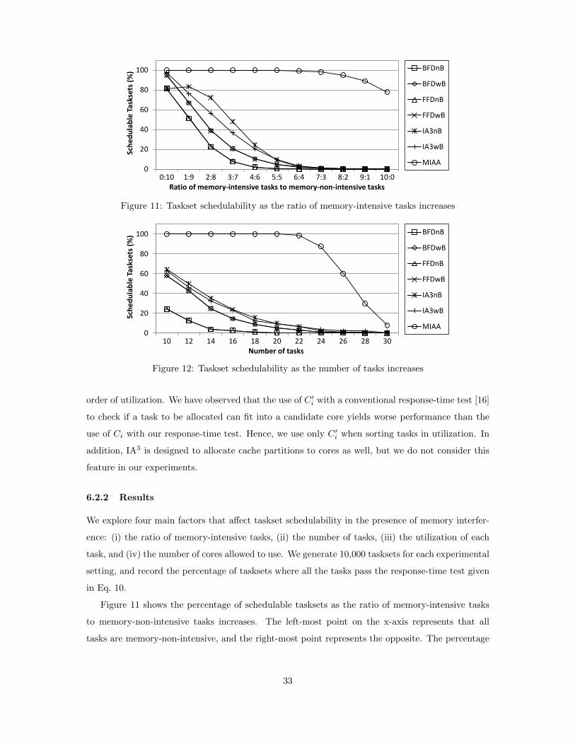
0
20
40
60
80
100
0:10 1:9 2:8 3:7 4:6 5:5 6:4 7:3 8:2 9:1 10:0
Sch
ed
ula
ble
Ta
skse
ts (
%)
Ratio of memory-intensive tasks to memory-non-intensive tasks
BFDnB
BFDwB
FFDnB
FFDwB
IA3nB
IA3wB
MIAA
Figure 11: Taskset schedulability as the ratio of memory-intensive tasks increases
0
20
40
60
80
100
10 12 14 16 18 20 22 24 26 28 30
Sch
ed
ula
ble
Ta
skse
ts (
%)
Number of tasks
BFDnB
BFDwB
FFDnB
FFDwB
IA3nB
IA3wB
MIAA
Figure 12: Taskset schedulability as the number of tasks increases
order of utilization. We have observed that the use of C ′i with a conventional response-time test [16]
to check if a task to be allocated can fit into a candidate core yields worse performance than the
use of Ci with our response-time test. Hence, we use only C ′i when sorting tasks in utilization. In
addition, IA3 is designed to allocate cache partitions to cores as well, but we do not consider this
feature in our experiments.
6.2.2 Results
We explore four main factors that affect taskset schedulability in the presence of memory interfer-
ence: (i) the ratio of memory-intensive tasks, (ii) the number of tasks, (iii) the utilization of each
task, and (iv) the number of cores allowed to use. We generate 10,000 tasksets for each experimental
setting, and record the percentage of tasksets where all the tasks pass the response-time test given
in Eq. 10.
Figure 11 shows the percentage of schedulable tasksets as the ratio of memory-intensive tasks
to memory-non-intensive tasks increases. The left-most point on the x-axis represents that all
tasks are memory-non-intensive, and the right-most point represents the opposite. The percentage
33
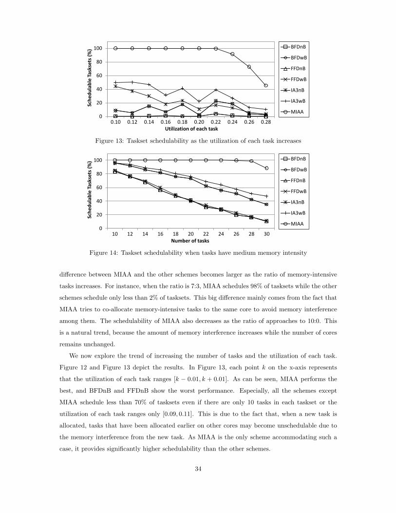
0
20
40
60
80
100
0.10 0.12 0.14 0.16 0.18 0.20 0.22 0.24 0.26 0.28
Sch
ed
ula
ble
Ta
skse
ts (
%)
Utilization of each task
BFDnB
BFDwB
FFDnB
FFDwB
IA3nB
IA3wB
MIAA
Figure 13: Taskset schedulability as the utilization of each task increases
0
20
40
60
80
100
10 12 14 16 18 20 22 24 26 28 30
Sch
ed
ula
ble
Ta
skse
ts (
%)
Number of tasks
BFDnB
BFDwB
FFDnB
FFDwB
IA3nB
IA3wB
MIAA
Figure 14: Taskset schedulability when tasks have medium memory intensity
difference between MIAA and the other schemes becomes larger as the ratio of memory-intensive
tasks increases. For instance, when the ratio is 7:3, MIAA schedules 98% of tasksets while the other
schemes schedule only less than 2% of tasksets. This big difference mainly comes from the fact that
MIAA tries to co-allocate memory-intensive tasks to the same core to avoid memory interference
among them. The schedulability of MIAA also decreases as the ratio of approaches to 10:0. This
is a natural trend, because the amount of memory interference increases while the number of cores
remains unchanged.
We now explore the trend of increasing the number of tasks and the utilization of each task.
Figure 12 and Figure 13 depict the results. In Figure 13, each point k on the x-axis represents
that the utilization of each task ranges [k − 0.01, k + 0.01]. As can be seen, MIAA performs the
best, and BFDnB and FFDnB show the worst performance. Especially, all the schemes except
MIAA schedule less than 70% of tasksets even if there are only 10 tasks in each taskset or the
utilization of each task ranges only [0.09, 0.11]. This is due to the fact that, when a new task is
allocated, tasks that have been allocated earlier on other cores may become unschedulable due to
the memory interference from the new task. As MIAA is the only scheme accommodating such a
case, it provides significantly higher schedulability than the other schemes.
34

0
20
40
60
80
100
8 9 10 11 12
Sch
ed
ula
ble
Ta
skse
ts (
%)
Number of cores
BFDnB
BFDwB
FFDnB
FFDwB
IA3nB
IA3wB
MIAA
Figure 15: Taskset schedulability as the number of cores increases
In Figure 14, we consider the case where tasks have medium memory intensity. For this purpose,
we randomly select the Hi value for each task in the range of [100, 10000]. The results in this figure
show that MIAA also outperforms the other schemes when tasks do not have a bimodal distribution
of memory intensity.
Lastly, we compare in Figure 15 the percentage of schedulable tasksets under different schemes
when the number of cores is more than the number of bank partitions. In this experiment, the
number of tasks per taskset is set to 25, and the Hi value and the utilization Ui of each task
are randomly selected from [100, 10000] and [0.2, 0.4], respectively. The percentage under MIAA
increases with the number of cores. Especially, MIAA can schedule 98% of tasksets with 11 cores.
However, the other schemes cannot schedule more than 70% of tasksets, even with 12 cores. These
experimental results show that a task allocation algorithm cannot scale well on multi-core platforms
without explicit consideration of memory interference and MIAA yields a significant improvement
in task schedulability compared to previous schemes. We expect that the performance of MIAA can
be further improved by elaborating the functions used by MIAA, such as LeastInterferingBank()
and ExtractMinCut(). This remains as part of future work.
7 Related Work
This paper builds upon the first work [17] that upper bounds the request re-ordering effect of COTS
memory controllers. The new contributions of this paper are as follows: (i) an extended analysis
for bounding memory interference delay in DRAM with multiple ranks, (ii) a memory interference-
aware task allocation algorithm (MIAA) that reduces the degree of memory interference, (iii) a
discussion on memory controllers with write batching, and (iv) experimental results exploring the
impact of multiple outstanding requests and latency hiding techniques. Specifically, to our knowl-
edge, MIAA is the first approach to mitigate memory interference while preserving schedulability
35

by co-allocating memory-intensive tasks on the same core with dedicated DRAM banks.
Researchers have developed special (non-COTS) components of memory systems for real-time
systems. The Predator memory controller [3] uses credit-based arbitration and closes an open row
after each access. The AMC memory controller [39] spreads the data of a single cache block across
all DRAM banks so as to reduce the impact of interference by serializing all memory requests. The
PRET DRAM controller [42] hardware partitions banks among cores for predictability. A memory
controller that allows different burst sizes for different memory requests has been proposed [27]. A
memory controller that partitions the set of banks so that a single memory access can fetch data
from multiple banks (bank interleaving) within a partition of banks has been proposed and it uses
the open-row policy [23]. Researchers have also proposed techniques that modify a program and
carefully set up time-triggered schedules so that there is no instant where two processor cores have
outstanding memory operations [44].
We have heard, however, a strong interest from software practitioners in techniques that can
use COTS multi-core processors and existing applications without requiring modifications and,
therefore, this has been the focus of this paper. In this context, some previous work considers the
entire memory system as a single resource, such that a processor core requests this resource when it
generates a cache miss and it must hold this resource exclusively until the data of the cache miss are
delivered to the processor core that requested it [40, 5, 9, 45, 30]. They commonly assumed that each
memory request takes a constant service time and memory requests from multiple cores are serviced
in the order of their arrival time. However, these assumptions may lead to overly pessimistic or
optimistic estimates in COTS systems, where the service time of each memory request varies and
the memory controller re-orders the memory requests [32].
Instead of considering the memory system as a single resource, recent work [51] makes a more
realistic assumption about the memory system, where the memory controller has one request queue
per DRAM bank and one system-wide queue connected to the per-bank queues. That analysis,
however, only considers the case where each processor core is assigned a private DRAM bank.
Unfortunately, the number of DRAM banks is growing more slowly than the number of cores, and
the memory space requirement of a workload in a core may exceed the size of a single bank. Due to
this limited availability of DRAM banks, it is necessary to consider sharing of DRAM banks among
multiple cores. With bank sharing, memory requests can be re-ordered in the per-bank queues,
thereby increasing memory request service times. The work in [51] unfortunately does not model
this request re-ordering effect. In this paper, we have eliminated this limitation.
In the field of task allocation, the problem of finding an optimal allocation of tasks to cores is
known to be NP-complete [15]. Hence, many near-optimal algorithms based on the bin-packing
heuristics have been proposed as practical solutions to the task allocation problem [10, 24, 25]. The
36

IA3 algorithm [38] is the first approach to take memory interference into account when allocating
tasks. IA3 pessimistically assumes that the amount of memory interference for a task is only affected
by the number of cores used, and does not consider the actual number of interfering memory requests
generated by other tasks that run in parallel. Unlike IA3, our memory interference-aware allocation
algorithm (MIAA) reduces memory interference by considering the memory access intensity of each
task. We have shown in Section 6 that our algorithm significantly outperforms IA3.
Finally, there has been recent work in the computer architecture community on the design of
memory controllers and memory systems that can dynamically estimate application slowdowns [47,
32, 11, 58]. These designs do not aim to provide worst-case bounds and can under-estimate memory
interference. Future memory controllers might incorporate ideas like batching and thread prioriti-
zation (e.g., [35, 22, 21, 46]). This will lead to a different analysis, which could be interesting future
work that builds on ours.
8 Conclusions and Future Work
In this paper, we have presented an analysis for bounding memory interference on a multi-core
platform with a COTS DRAM system. Our analysis is based on a realistic memory model, which
considers the JEDEC DDR3 SDRAM standard, the FR-FCFS policy of the memory controller, and
shared/private DRAM banks. To provide a tighter upper-bound on the memory interference delay,
our analysis uses the combination of the request-driven and job-driven approaches. Experimental
results from a real hardware platform show that, although some of our assumptions do not hold in
the platform used, our analysis can closely estimate the memory interference delay under workloads
with both high and low memory contention.
We have also presented a memory interference-aware task allocation algorithm that accommo-
dates memory interference delay during the task allocation phase. Experimental results indicate
that our algorithm yields significant benefits in task schedulability, with as much as 96% more
tasksets being schedulable than previous schemes.
As multi-core processors are already ubiquitous, contention in shared main memory should be
seriously considered and mitigated. We believe that our analysis and task allocation algorithm
can be effectively used for designing predictable multi-core real-time systems. We believe plenty of
future work exists in this area. We plan to (i) explore the effect of hardware prefetchers on memory
interference delay, (ii) examine a non-timing-compositional architecture that allows out-of-order
execution and multiple outstanding cache misses, and (iii) examine the effects of upcoming memory
schedulers that serve heterogeneous agents.
37
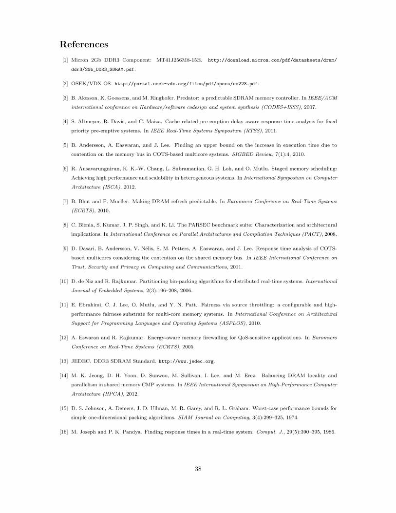
References
[1] Micron 2Gb DDR3 Component: MT41J256M8-15E. http://download.micron.com/pdf/datasheets/dram/
ddr3/2Gb_DDR3_SDRAM.pdf.
[2] OSEK/VDX OS. http://portal.osek-vdx.org/files/pdf/specs/os223.pdf.
[3] B. Akesson, K. Goossens, and M. Ringhofer. Predator: a predictable SDRAM memory controller. In IEEE/ACM
international conference on Hardware/software codesign and system synthesis (CODES+ISSS), 2007.
[4] S. Altmeyer, R. Davis, and C. Maiza. Cache related pre-emption delay aware response time analysis for fixed
priority pre-emptive systems. In IEEE Real-Time Systems Symposium (RTSS), 2011.
[5] B. Andersson, A. Easwaran, and J. Lee. Finding an upper bound on the increase in execution time due to
contention on the memory bus in COTS-based multicore systems. SIGBED Review, 7(1):4, 2010.
[6] R. Ausavarungnirun, K. K.-W. Chang, L. Subramanian, G. H. Loh, and O. Mutlu. Staged memory scheduling:
Achieving high performance and scalability in heterogeneous systems. In International Symposium on Computer
Architecture (ISCA), 2012.
[7] B. Bhat and F. Mueller. Making DRAM refresh predictable. In Euromicro Conference on Real-Time Systems
(ECRTS), 2010.
[8] C. Bienia, S. Kumar, J. P. Singh, and K. Li. The PARSEC benchmark suite: Characterization and architectural
implications. In International Conference on Parallel Architectures and Compilation Techniques (PACT), 2008.
[9] D. Dasari, B. Andersson, V. Nelis, S. M. Petters, A. Easwaran, and J. Lee. Response time analysis of COTS-
based multicores considering the contention on the shared memory bus. In IEEE International Conference on
Trust, Security and Privacy in Computing and Communications, 2011.
[10] D. de Niz and R. Rajkumar. Partitioning bin-packing algorithms for distributed real-time systems. International
Journal of Embedded Systems, 2(3):196–208, 2006.
[11] E. Ebrahimi, C. J. Lee, O. Mutlu, and Y. N. Patt. Fairness via source throttling: a configurable and high-
performance fairness substrate for multi-core memory systems. In International Conference on Architectural
Support for Programming Languages and Operating Systems (ASPLOS), 2010.
[12] A. Eswaran and R. Rajkumar. Energy-aware memory firewalling for QoS-sensitive applications. In Euromicro
Conference on Real-Time Systems (ECRTS), 2005.
[13] JEDEC. DDR3 SDRAM Standard. http://www.jedec.org.
[14] M. K. Jeong, D. H. Yoon, D. Sunwoo, M. Sullivan, I. Lee, and M. Erez. Balancing DRAM locality and
parallelism in shared memory CMP systems. In IEEE International Symposium on High-Performance Computer
Architecture (HPCA), 2012.
[15] D. S. Johnson, A. Demers, J. D. Ullman, M. R. Garey, and R. L. Graham. Worst-case performance bounds for
simple one-dimensional packing algorithms. SIAM Journal on Computing, 3(4):299–325, 1974.
[16] M. Joseph and P. K. Pandya. Finding response times in a real-time system. Comput. J., 29(5):390–395, 1986.
38
[17] H. Kim, D. de Niz, B. Andersson, M. Klein, O. Mutlu, and R. R. Rajkumar. Bounding memory interference
delay in COTS-based multi-core systems. In IEEE Real-Time Technology and Applications Symposium (RTAS),
2014.
[18] H. Kim, A. Kandhalu, and R. Rajkumar. A coordinated approach for practical OS-level cache management in
multi-core real-time systems. In Euromicro Conference on Real-Time Systems (ECRTS), 2013.
[19] H. Kim, J. Kim, and R. R. Rajkumar. A profiling framework in Linux/RK and its application. In Open Demo
Session of IEEE Real-Time Systems Symposium (RTSS@Work), 2012.
[20] H. Kim and R. Rajkumar. Shared-page management for improving the temporal isolation of memory reservations
in resource kernels. In IEEE Conference on Embedded and Real-Time Computing Systems and Applications
(RTCSA), 2012.
[21] Y. Kim, D. Han, O. Mutlu, and M. Harchol-Balter. ATLAS: A scalable and high-performance scheduling
algorithm for multiple memory controllers. In IEEE International Symposium on High-Performance Computer
Architecture (HPCA), 2010.
[22] Y. Kim, M. Papamichael, O. Mutlu, and M. Harchol-Balter. Thread cluster memory scheduling: Exploiting dif-
ferences in memory access behavior. In IEEE/ACM International Symposium on Microarchitecture (MICRO),
2010.
[23] Y. Krishnapillai, Z. P. Wu, and R. Pellizzoni. A rank-switching, open-row DRAM controller for mixed-criticality
systems. In Euromicro Conference on Real-Time Systems (ECRTS), 2014.
[24] K. Lakshmanan, D. de Niz, R. Rajkumar, and G. Moreno. Resource allocation in distributed mixed-criticality
cyber-physical systems. In IEEE International Conference on Distributed Computing Systems (ICDCS), 2010.
[25] K. Lakshmanan, R. Rajkumar, and J. P. Lehoczky. Partitioned fixed-priority preemptive scheduling for multi-
core processors. In Euromicro Conference on Real-Time Systems (ECRTS), 2009.
[26] C. J. Lee, V. Narasiman, E. Ebrahimi, O. Mutlu, and Y. N. Patt. DRAM-aware last-level cache writeback:
Reducing write-caused interference in memory systems. Technical Report TR-HPS-2010-002, UT Austin, 2010.
[27] Y. Li, B. Akesson, and K. Goossens. Dynamic command scheduling for real-time memory controllers. In
Euromicro Conference on Real-Time Systems (ECRTS), 2014.
[28] C. L. Liu and J. W. Layland. Scheduling algorithms for multiprogramming in a hard-real-time environment. J.
ACM, 20(1):46–61, 1973.
[29] L. Liu, Z. Cui, M. Xing, Y. Bao, M. Chen, and C. Wu. A software memory partition approach for eliminat-
ing bank-level interference in multicore systems. In International Conference on Parallel Architectures and
Compilation Techniques (PACT), 2012.
[30] M. Lv, G. Nan, W. Yi, and G. Yu. Combining abstract interpretation with model checking for timing analysis
of multicore software. In IEEE Real-Time Systems Symposium (RTSS), 2010.
[31] J. D. McCalpin. STREAM: Sustainable memory bandwidth in high performance computers. http://www.cs.
virginia.edu/stream.
[32] T. Moscibroda and O. Mutlu. Memory performance attacks: Denial of memory service in multi-core systems.
In USENIX Security Symposium, 2007.
39
[33] S. P. Muralidhara, L. Subramanian, O. Mutlu, M. Kandemir, and T. Moscibroda. Reducing memory inter-
ference in multicore systems via application-aware memory channel partitioning. In IEEE/ACM International
Symposium on Microarchitecture (MICRO), 2011.
[34] O. Mutlu and T. Moscibroda. Stall-time fair memory access scheduling for chip multiprocessors. In IEEE/ACM
International Symposium on Microarchitecture (MICRO), 2007.
[35] O. Mutlu and T. Moscibroda. Parallelism-aware batch scheduling: Enhancing both performance and fairness of
shared DRAM systems. In International Symposium on Computer Architecture (ISCA), 2008.
[36] K. J. Nesbit, N. Aggarwal, J. Laudon, and J. E. Smith. Fair queuing memory systems. In IEEE/ACM
International Symposium on Microarchitecture (MICRO), 2006.
[37] S. Oikawa and R. Rajkumar. Linux/RK: A portable resource kernel in Linux. In IEEE Real-Time Systems
Symposium (RTSS) Work-In-Progress, 1998.
[38] M. Paolieri, E. Quinones, F. Cazorla, R. Davis, and M. Valero. IA3: An interference aware allocation algorithm
for multicore hard real-time systems. In IEEE Real-Time Technology and Applications Symposium (RTAS),
2011.
[39] M. Paolieri, E. Quinones, F. Cazorla, and M. Valero. An analyzable memory controller for hard read-time
CMPs. IEEE Embedded Systems Letters, 1(4):86–90, 2010.
[40] R. Pellizzoni, A. Schranzhofer, J. Chen, M. Caccamo, and L. Thiele. Worst case delay analysis for memory
interference in multicore systems. In Design, Automation Test in Europe Conference Exhibition (DATE), 2010.
[41] R. Rajkumar, K. Juvva, A. Molano, and S. Oikawa. Resource kernels: A resource-centric approach to real-time
and multimedia systems. In SPIE/ACM Conference on Multimedia Computing and Networking, 1998.
[42] J. Reineke, I. Liu, H. D. Patel, S. Kim, and E. A. Lee. PRET DRAM controller: Bank privatization for
predictability and temporal isolation. In IEEE/ACM international conference on Hardware/software codesign
and system synthesis (CODES+ISSS), 2011.
[43] S. Rixner, W. J. Dally, U. J. Kapasi, P. Mattson, and J. D. Owens. Memory access scheduling. In International
Symposium on Computer Architecture (ISCA), 2000.
[44] J. Rosen, A. Andrei, P. Eles, and Z. Peng. Bus access optimization for predictable implementation of real-time
applications on multiprocessor systems-on-chip. In IEEE Real-Time Systems Symposium (RTSS), 2007.
[45] S. Schliecker, M. Negrean, and R. Ernst. Bounding the shared resource load for the performance analysis of
multiprocessor systems. In Design, Automation Test in Europe Conference Exhibition (DATE), 2010.
[46] L. Subramanian, D. Lee, V. Seshadri, H. Rastogi, and O. Mutlu. The blacklisting memory scheduler: Achieving
high performance and fairness at low cost. In IEEE International Conference on Computer Design (ICCD),
2014.
[47] L. Subramanian, V. Seshadri, Y. Kim, B. Jaiyen, and O. Mutlu. MISE: Providing performance predictability and
improving fairness in shared main memory systems. In IEEE International Symposium on High-Performance
Computer Architecture (HPCA), 2013.
40

[48] N. Suzuki, H. Kim, D. de Niz, B. Andersson, L. Wrage, M. Klein, and R. R. Rajkumar. Coordinated bank and
cache coloring for temporal protection of memory accesses. In IEEE International Conference on Embedded
Software and Systems (ICESS), 2013.
[49] R. Wilhelm, D. Grund, J. Reineke, M. Schlickling, M. Pister, and C. Ferdinand. Memory hierarchies, pipelines,
and buses for future architectures in time-critical embedded systems. IEEE Transactions on Computer-Aided
Design of Integrated Circuits and Systems, 28(7):966–978, 2009.
[50] Windriver VxWorks. http://www.windriver.com.
[51] Z. P. Wu, Y. Krish, and R. Pellizzoni. Worst case analysis of DRAM latency in multi-requestor systems. In
IEEE Real-Time Systems Symposium (RTSS), 2013.
[52] M. Xie, D. Tong, K. Huang, and X. Cheng. Improving system throughput and fairness simultaneously in CMP
systems via dynamic bank partitioning. In IEEE International Symposium on High-Performance Computer
Architecture (HPCA), 2014.
[53] H. Yun, R. Mancuso, Z.-P. Wu, and R. Pellizzoni. PALLOC: DRAM bank-aware memory allocator for perfor-
mance isolation on multicore platforms. In IEEE Real-Time Technology and Applications Symposium (RTAS),
2014.
[54] H. Yun, G. Yao, R. Pellizzoni, M. Caccamo, and L. Sha. Memory access control in multiprocessor for real-time
systems with mixed criticality. In Euromicro Conference on Real-Time Systems (ECRTS), 2012.
[55] X. Zhang, S. Dwarkadas, and K. Shen. Hardware execution throttling for multi-core resource management. In
USENIX Annual Technical Conference (USENIX ATC), 2009.
[56] W. K. Zuravleff and T. Robinson. Controller for a synchronous DRAM that maximizes throughput by allowing
memory requests and commands to be issued out of order. U.S. Patent Number 5,630,096, 1997.
[57] V. Seshadri, A. Bhowmick, O. Mutlu, P. B. Gibbons, M. Kozuch, T. C. Mowry, et al. The dirty-block index.
In International Symposium on Computer Architecture (ISCA), 2014.
[58] L. Subramanian, V. Seshadri, A. Ghosh, S. Khan, and O. Mutlu. The application slowdown model: Quantifying
and controlling the impact of inter-application interference at shared caches and main memory. In IEEE/ACM
International Symposium on Microarchitecture (MICRO), 2015.
41