boolean algebra & logic gates - weebly · a logic gate used to perform logical multiplication...
TRANSCRIPT

Basics of Digital Systems Dept. of ECE
KL University, Guntur
BOOLEAN ALGEBRA & LOGIC GATES
Logic gates are electronic circuits that can be used to implement the most elementary logic
expressions, also known as Boolean expressions. The logic gate is the most basic building
block of combinational logic. There are three basic logic gates, namely the OR gate, the AND
gate and the NOT gate. Other logic gates that are derived from these basic gates are the
NAND gate, the NOR gate, the EXCLUSIVEOR gate and the EXCLUSIVE-NOR gate. This
chapter deals with logic gates and implementations using NAND and NOR gates followed by
simplification of Boolean functions using Boolean Laws and theorems and using K-maps.
Positive and Negative Logic
The binary variables can have either of the two states, i.e. the logic ‘0’ state or the logic ‘1’
state. These logic states in digital systems such as computers, for instance, are represented by
two different voltage levels or two different current levels. If the more positive of the two
voltage or current levels represents a logic ‘1’ and the less positive of the two levels
represents a logic ‘0’, then the logic system is referred to as a positive logic system. If the
more positive of the two voltage or current levels represents a logic ‘0’ and the less positive
of the two levels represents a logic ‘1’, then the logic system is referred to as a negative logic
system.
If the two voltage levels are 0 V and +5 V, then in the positive logic system the 0 V
represents logic ‘0’ and the +5 V represents logic ‘1’. In the negative logic system, 0 V
represents logic ‘1’ and 5 V represents logic ‘0’. If the two voltage levels are 0 V and −5 V,
then in the positive logic system the 0 V represents a logic ‘1’ and the −5 V represents a logic
‘0’. In the negative logic system, 0 V represents logic ‘0’ and −5 V represents logic ‘1’.
Logic Gates
The logic gate is the most basic building block of any digital system, including computers.
Each one of the basic logic gates is a piece of hardware or an electronic circuit that can be
used to implement some basic logic expression. While laws of Boolean algebra could be used
to do manipulation with binary variables and simplify logic expressions, these are actually
implemented in a digital system with the help of electronic circuits called logic gates. The
three basic logic gates are the OR gate, the AND gate and the NOT gate.

Basics of Digital Systems Dept. of ECE
KL University, Guntur
OR Gate
A logic gate used to perform the operation of logical addition is called an OR gate. An OR
gate performs an ORing operation on two or more than two logic variables. The OR operation
on two independent logic variables A and B is written as Y = A+B and reads as Y equals A
OR B. An OR gate is a logic circuit with two or more inputs and one output. The output of an
OR gate is LOW only when all of its inputs are LOW. For all other possible input
combinations, the output is HIGH. A truth table lists all possible combinations of input binary
variables and the corresponding outputs of a logic system. Figure shows the circuit symbol
and the truth table of a two-input OR gate. The operation of a two-input OR gate is explained
by the logic expression
Y = A+B
Two input OR Gate
AND Gate
A logic gate used to perform logical multiplication is known as AND gate. An AND gate is a
logic circuit having two or more inputs and one output. The output of an AND gate is HIGH
only when all of its inputs are in the HIGH state. In all other cases, the output is LOW. The
logic symbol and truth table of a two-input AND gate is shown in figure. The AND operation
on two independent logic variables A and B is written as Y = A.B and reads as Y equals A
AND B. The operation of a two-input AND gate is explained by the logic expression
Y = A.B
Two input AND Gate
Basics of Digital Systems Dept. of ECE
KL University, Guntur
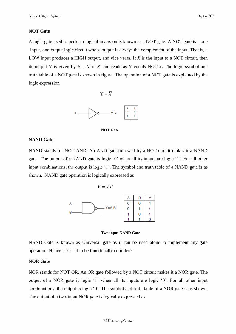
NOT Gate
A logic gate used to perform logical inversion is known as a NOT gate. A NOT gate is a one
-input, one-output logic circuit whose output is always the complement of the input. That is, a
LOW input produces a HIGH output, and vice versa. If is the input to a NOT circuit, then
its output Y is given by Y = ̅ or and reads as Y equals NOT . The logic symbol and
truth table of a NOT gate is shown in figure. The operation of a NOT gate is explained by the
logic expression
Y = ̅
NOT Gate
NAND Gate
NAND stands for NOT AND. An AND gate followed by a NOT circuit makes it a NAND
gate. The output of a NAND gate is logic ‘0’ when all its inputs are logic ‘1’. For all other
input combinations, the output is logic ‘1’. The symbol and truth table of a NAND gate is as
shown. NAND gate operation is logically expressed as
Two input NAND Gate
NAND Gate is known as Universal gate as it can be used alone to implement any gate
operation. Hence it is said to be functionally complete.
NOR Gate
NOR stands for NOT OR. An OR gate followed by a NOT circuit makes it a NOR gate. The
output of a NOR gate is logic ‘1’ when all its inputs are logic ‘0’. For all other input
combinations, the output is logic ‘0’. The symbol and truth table of a NOR gate is as shown.
The output of a two-input NOR gate is logically expressed as

Basics of Digital Systems Dept. of ECE
KL University, Guntur
Two input NOR Gate
NOR gate is also known as Universal gate as it is used alone to implement any gate operation
and hence it is also functionally complete.
EXCLUSIVE-OR Gate
The EXCLUSIVE-OR gate, commonly written as EX-OR gate, is a two-input, one-output
gate. The output of an EX-OR gate is logic ‘1’ when the inputs are unlike and logic ‘0’ when
the inputs are like. Although EX-OR gates are available in integrated circuit form only as
two-input gates, unlike other gates which are available in multiple inputs also, multiple-input
EX-OR logic functions can be implemented using more than one two-input gates. The output
of a multiple-input EX-OR logic function is logic ‘1’ when the number of 1s in the input
sequence is odd and logic ‘0’ when the number of 1s in the input sequence is even, including
zero. The symbol and truth table of an EX-OR gate is shown in figure. The output of a two-
input EX-OR gate is logically expressed as
Two input EX-OR Gate
EXCLUSIVE-NOR Gate
EXCLUSIVE-NOR (commonly written as EX-NOR) means NOT of EX-OR, i.e. the logic
gate that we get by complementing the output of an EX-OR gate. The truth table of an EX-
NOR gate is obtained from the truth table of an EX-OR gate by complementing the output
entries as shown in figure. Logically,

Basics of Digital Systems Dept. of ECE
KL University, Guntur
Two input EX-NOR Gate
The output of a two-input EX-NOR gate is logic ‘1’ when the inputs are like and logic ‘0’
when they are unlike. In general, the output of a multiple-input EX-NOR logic function is
logic ‘0’ when the number of 1s in the input sequence is odd and a logic ‘1’ when the number
of 1s in the input sequence is even including zero.
Boolean algebra:
Boolean algebra is an algebraic structure defined on a set of elements B together with two
binary operators + and · provided the following postulates are satisfied:
1. a) Closure with respect to the operator +.
b) Closure with respect to the operator ·.
2. a) An identity element with respect to +, designated by 0:
b) An identity element with respect to ·, designated by 1: .
3. a) Commutative with respect to +:
b) Commutative with respect to ·:
4. a) · is distributive over +:
b) + is distributive over ·:
5. For every element there exists an element (complement of ) such that
and
Boolean Laws & Theorems:
Duality Principle:
It states that every algebraic expression deducible from the postulates of Boolean algebra
remains valid if the operators and identity elements are interchanged. If the dual of an
algebraic expression is desired, OR and AND operators are interchanged and 1’s are replaced
by 0’s and 0’s by 1’s.
Basics of Digital Systems Dept. of ECE
KL University, Guntur
DeMorgan’s Theorem:
Absorption Theorem:
Simplification using Boolean Laws & Theorems:
The Boolean functions can be simplified by using appropriate Boolean laws and theorems.
Examples:
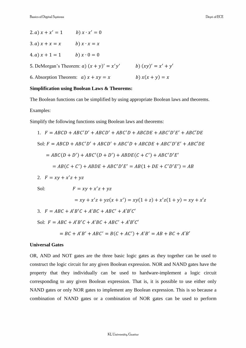
Simplify the following functions using Boolean laws and theorems:
1.
Sol:
2.
Sol:
3.
Sol:
Universal Gates
OR, AND and NOT gates are the three basic logic gates as they together can be used to
construct the logic circuit for any given Boolean expression. NOR and NAND gates have the
property that they individually can be used to hardware-implement a logic circuit
corresponding to any given Boolean expression. That is, it is possible to use either only
NAND gates or only NOR gates to implement any Boolean expression. This is so because a
combination of NAND gates or a combination of NOR gates can be used to perform

Basics of Digital Systems Dept. of ECE
KL University, Guntur
functions of any of the basic logic gates. It is for this reason that NAND and NOR gates are
universal gates.
Implementation of gates using NAND gates
a) NOT gate:
b) AND gate:
c) OR gate:
d) NOR gate:
e) Ex-OR gate:
f) Ex-NOR gate:
Basics of Digital Systems Dept. of ECE
KL University, Guntur
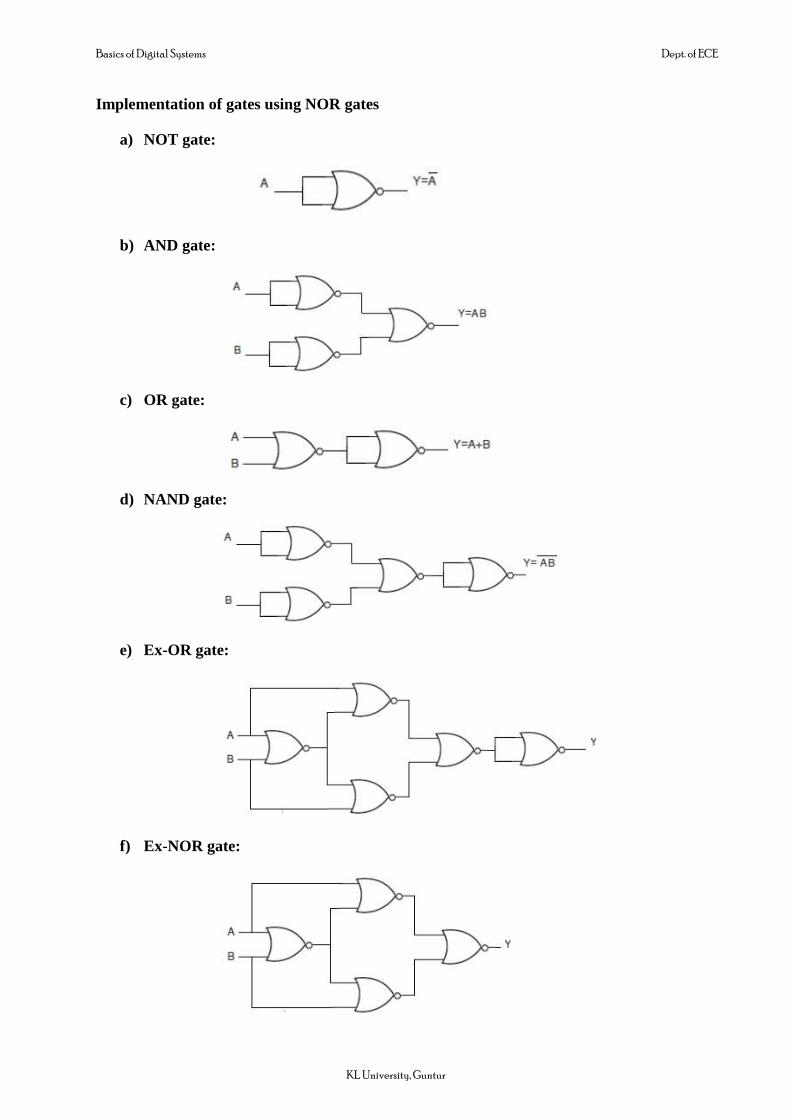
Implementation of gates using NOR gates
a) NOT gate:
b) AND gate:
c) OR gate:
d) NAND gate:
e) Ex-OR gate:
f) Ex-NOR gate:
Basics of Digital Systems Dept. of ECE
KL University, Guntur
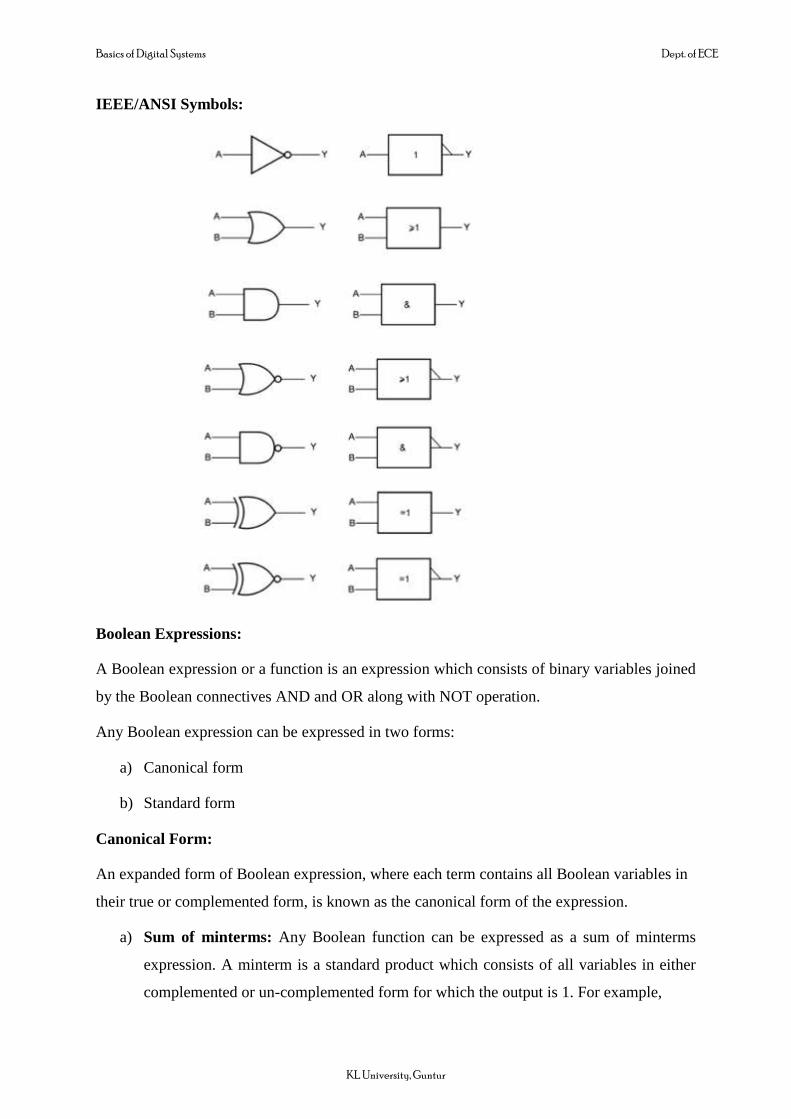
IEEE/ANSI Symbols:
Boolean Expressions:
A Boolean expression or a function is an expression which consists of binary variables joined
by the Boolean connectives AND and OR along with NOT operation.
Any Boolean expression can be expressed in two forms:
a) Canonical form
b) Standard form
Canonical Form:
An expanded form of Boolean expression, where each term contains all Boolean variables in
their true or complemented form, is known as the canonical form of the expression.
a) Sum of minterms: Any Boolean function can be expressed as a sum of minterms
expression. A minterm is a standard product which consists of all variables in either
complemented or un-complemented form for which the output is 1. For example,

Basics of Digital Systems Dept. of ECE
KL University, Guntur
∑
is a sum of minterms expression with three variables.
b) Product of maxterms: Any Boolean function can be expressed as a product of
maxterms expression. A maxterm is a standard sum which consists of all variables in
either complemented or un-complemented form for which the output is 0. For
example,
∏
is a product of maxterms expression with three variables.
Standard Form:
A simplified form of a Boolean expression which may consist of one or more number of
variables in each term in either complemented or un-complemented form, is known as
Standard form of the expression.
a) Sum of Products (SOP): The sum of products is a Boolean expression containing
AND terms, called Product terms, of one or more literals each; the sum denotes the
ORing of these terms. For example,
is a SOP expression with three variables.
b) Product of Sums (POS): It is a Boolean expression containing OR terms called Sum
terms and the product denotes the ANDing of these terms.
is a POS expression with three variables.
** Canonical form is obtained when a function is taken from a truth table. When
implementing a Boolean function with gates, standard form is preferred.
Simplification of Boolean expressions:
The primary objective of all simplification procedures is to obtain an expression that has the
minimum number of terms. Obtaining an expression with the minimum number of literals is
usually the secondary objective. The Boolean functions can be simplified by using
Basics of Digital Systems Dept. of ECE
KL University, Guntur
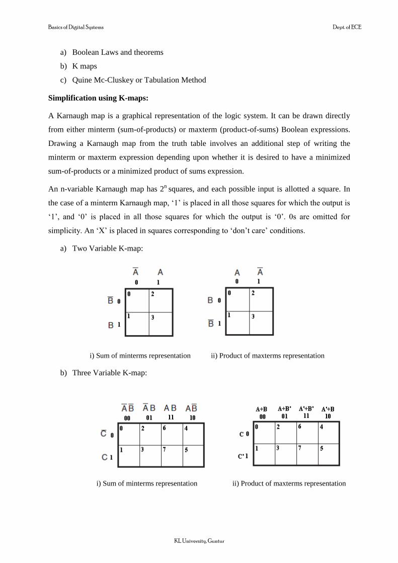
a) Boolean Laws and theorems
b) K maps
c) Quine Mc-Cluskey or Tabulation Method
Simplification using K-maps:
A Karnaugh map is a graphical representation of the logic system. It can be drawn directly
from either minterm (sum-of-products) or maxterm (product-of-sums) Boolean expressions.
Drawing a Karnaugh map from the truth table involves an additional step of writing the
minterm or maxterm expression depending upon whether it is desired to have a minimized
sum-of-products or a minimized product of sums expression.
An n-variable Karnaugh map has 2n
squares, and each possible input is allotted a square. In
the case of a minterm Karnaugh map, ‘1’ is placed in all those squares for which the output is
‘1’, and ‘0’ is placed in all those squares for which the output is ‘0’. 0s are omitted for
simplicity. An ‘X’ is placed in squares corresponding to ‘don’t care’ conditions.
a) Two Variable K-map:
i) Sum of minterms representation ii) Product of maxterms representation
b) Three Variable K-map:
i) Sum of minterms representation ii) Product of maxterms representation

Basics of Digital Systems Dept. of ECE
KL University, Guntur
c) Four Variable K-map:
i) Sum of minterms representation ii) Product of maxterms representation
d) Five Variable K-map:
Simplification Algorithm:
Simplification of logical functions using K-maps is based on the principle of combining
terms in adjacent cells. Two cells are said to be adjacent if they differ in only one variable.
1. Identify the ones which cannot be combined with any other ones and encircle them.
These are called essential prime implicants.
2. Identify the ones that can be combined in groups of two in only one way. Encircle
them.
3. Identify the ones that can be combined with three other ones, to make a group of four
adjacent ones, in only one way. Encircle such group of ones.
4. Identify the ones that can be combined with seven other ones, to make a group of
eight adjacent ones, in only one way. Encircle them.
Basics of Digital Systems Dept. of ECE
KL University, Guntur
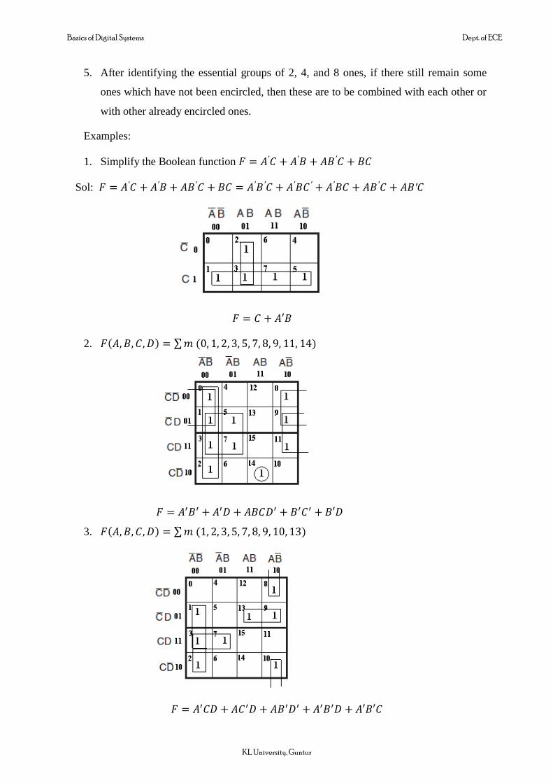
5. After identifying the essential groups of 2, 4, and 8 ones, if there still remain some
ones which have not been encircled, then these are to be combined with each other or
with other already encircled ones.
Examples:
1. Simplify the Boolean function
Sol:
2. ∑
3. ∑
Basics of Digital Systems Dept. of ECE
KL University, Guntur
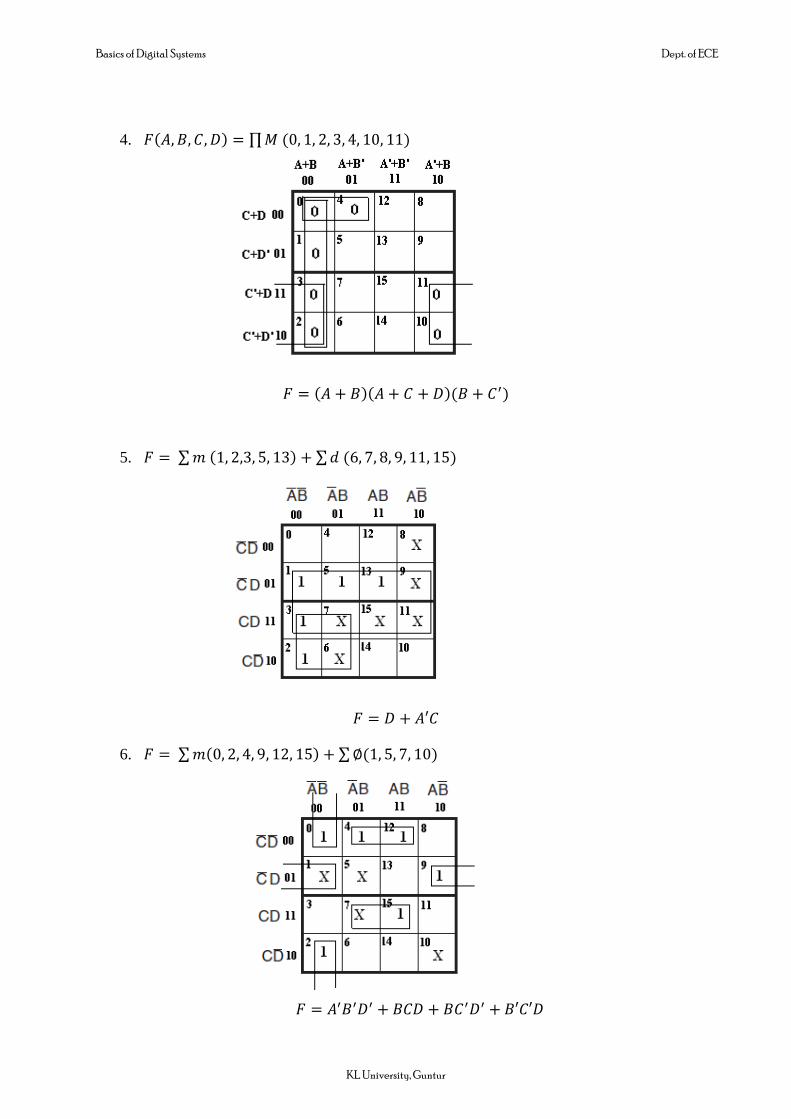
4. ∏
5. ∑ ∑
6. ∑ ∑

Basics of Digital Systems Dept. of ECE
KL University, Guntur
Quine Mc-Cluskey or Tabulation Method:
The K-map method is suitable for simplification of Boolean functions up to 5 or 6 variables.
As the number of variables increases beyond this, the visualization of adjacent squares is
difficult as the geometry is more involved. In case of more variables, Quine Mc-Cluskey
technique or Tabulation method is used which is a systematic procedure.
Procedure for Finding the Minimal Expression
1. Arrange all minterms in groups, such that all terms in the same group have same number of
1’s in their binary representation. Start with the least number of 1’s and continue with
grouping of increasing number of 1’s the number of 1’s in each term is called the index of
that term i.e., all the minterms of some index are placed in a some group. The lowest of value
index is zero. Separate each group by a thick line. This constitutes the 1st stage.
2. Compare every term of the lowest index (say i) group with each term in the successive
group of index (say, i + 1). If two minterms differ only one variable, that variable should be
removed and a dash (–) is placed at the position, thus a new term with only less literal is
formed. If such a situation occurs, a check mark is placed next to both minterms. After all
pairs of terms with indices i and (i + 1) have been considered, a thick line is drawn under the
last terms. When the above process has been repeated for all the groups of 1st stage, one stage
of elimination have been completed. This constitutes the 2nd
stage.
3. The 3rd
stage of elimination should be repeated of the nearly formed groups of second
stage. In this stage, two terms can be compared only than they have dashes in some positions.
The process continues to next higher stages until no further comparisons are possible. (i.e., no
further elimination of literals).
4. All terms which remain unchecked during the process are considered to be prime
implicants (PIs). Thus, a set of all PIs of the function is obtained.
5. From the set of all prime implicants, a set of essential prime implicants (EPIs) must be
determined by preparing prime implicant chart as follow.
(a) The PIs should be represented m rows and each minterm of the function in a column.
(b) Crosses should be placed in each row to show composition of minterms that makes the
PIs.
(c) A complete PIs chart should be inspected for columns containing only a single cross. PIs
that cover minterms with a single cross in their column are called EPIs.
Basics of Digital Systems Dept. of ECE
KL University, Guntur
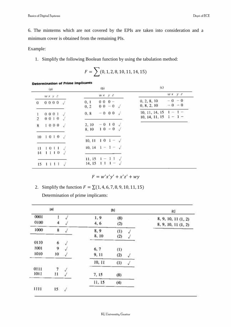
6. The minterms which are not covered by the EPIs are taken into consideration and a
minimum cover is obtained from the remaining PIs.
Example:
1. Simplify the following Boolean function by using the tabulation method:
∑
2. Simplify the function ∑
Determination of prime implicants:

Basics of Digital Systems Dept. of ECE
KL University, Guntur
All the minterms are covered by the prime implicants, except 7 and 15. Hence for 7 and 15,
the term is common and hence it will be included in the final expression.
Therefore
Basics of Digital Systems Dept. of ECE
KL University, Guntur
Two level Implementation:
Any logic circuit can be implemented in two levels by representing the Boolean function
either in SOP or POS form. Two level NAND and NOR circuits can be obtained by
representing the expression in SOP and POS form respectively. Minimum propagation delay
will be obtained by using two level implementation. But as the number of terms increases, the
number of inputs increases for the second level gate.
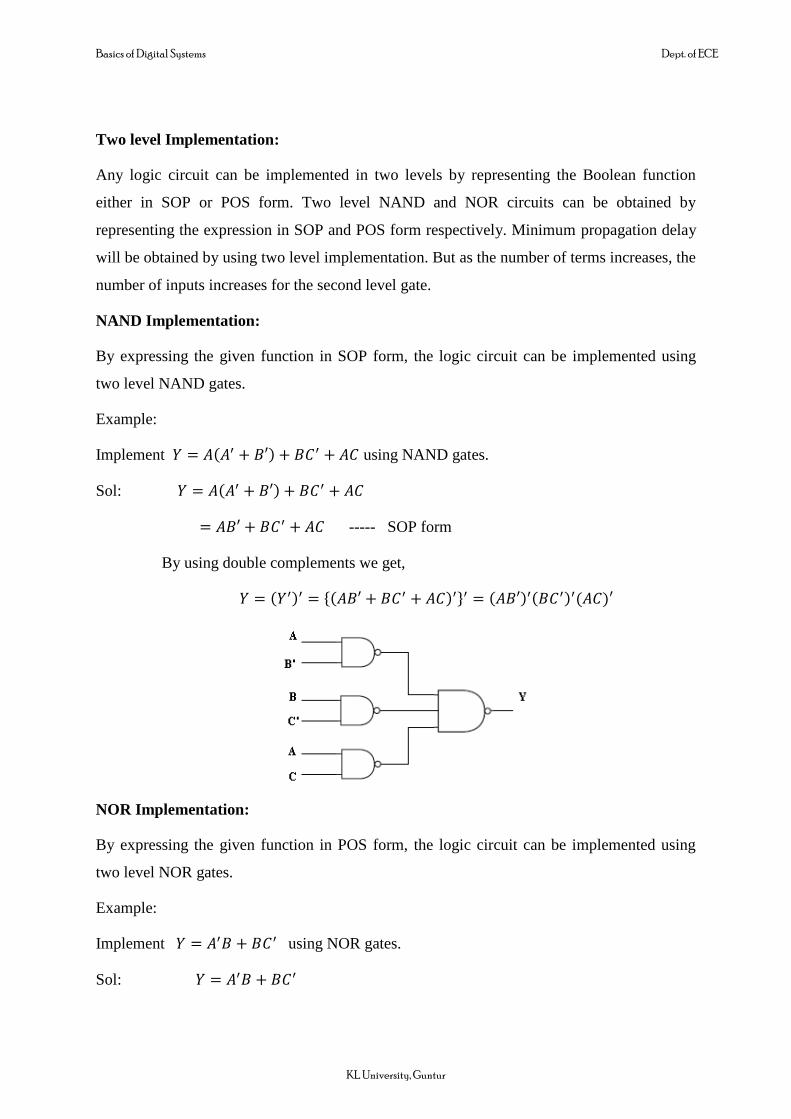
NAND Implementation:
By expressing the given function in SOP form, the logic circuit can be implemented using
two level NAND gates.
Example:
Implement using NAND gates.
Sol:
----- SOP form
By using double complements we get,
{ }
NOR Implementation:
By expressing the given function in POS form, the logic circuit can be implemented using
two level NOR gates.
Example:
Implement using NOR gates.
Sol:

Basics of Digital Systems Dept. of ECE
KL University, Guntur
……. Distributive law
……. Distributive law
and the expression is in POS form.
[{ } ]
[ ]
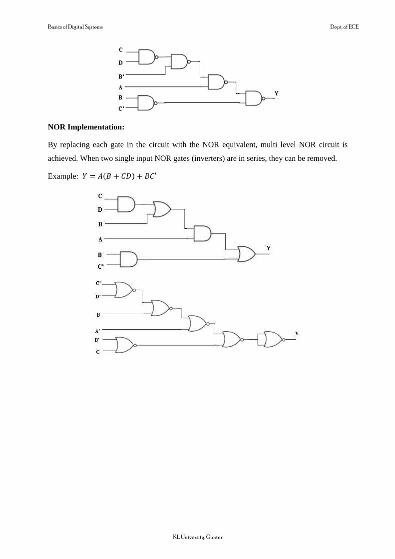
Multilevel Implementation:
Multi level NAND or NOR implementation of a Boolean circuit can be achieved by replacing
each gate in the circuit with the NAND or NOR equivalent circuits respectively. With this
type of implementation, very large propagation delay is achieved and only two input gates are
required.
NAND Implementation:
By replacing each gate in the circuit with the NAND equivalent, multi level NAND circuit is
achieved. When two single input NAND gates (inverters) are in series, they can be removed.
Example:
Basics of Digital Systems Dept. of ECE
KL University, Guntur
NOR Implementation:
By replacing each gate in the circuit with the NOR equivalent, multi level NOR circuit is
achieved. When two single input NOR gates (inverters) are in series, they can be removed.
Example: