bi-directional dc/dc converter topology … instruments 3 september 2016 poer supp esn semnar 201617...
TRANSCRIPT

Bidirectional DC/DC converter topology comparison and design
Zhong YeSystem Engineer
Sanatan RajagopalanFirmware Engineer
High Voltage Power SolutionsTexas Instruments
Texas Instruments 2 September 2016
Power Supply Design Seminar 2016/17
Introduction
Many emerging applications require energy to be
transferable between two ports bidirectionally. The
two applications discussed in this paper using
a low-voltage bidirectional DC/DC converter are
a 48-V/12-V automotive dual-bus system and a
server local energy storage (LES) system. These
systems do not normally require isolation. For
different systems, the reason and purpose for
using bidirectional DC/DC converters can be quite
different. With more and more electrification in
automotive designs, the power demands for start-
stop cars and micro-hybrid electric vehicles (HEVs)
have increased significantly – approaching 3 kW of a
12-V power-supply limit.
A mild HEV demands much higher power. Over
200 A of current distributed on a 12-V bus requires
a larger copper-wire cross-section, which increases
system cost. Besides high-current-distribution
conduction loss, 12-V high-power equipment
becomes less efficient and has higher loss with
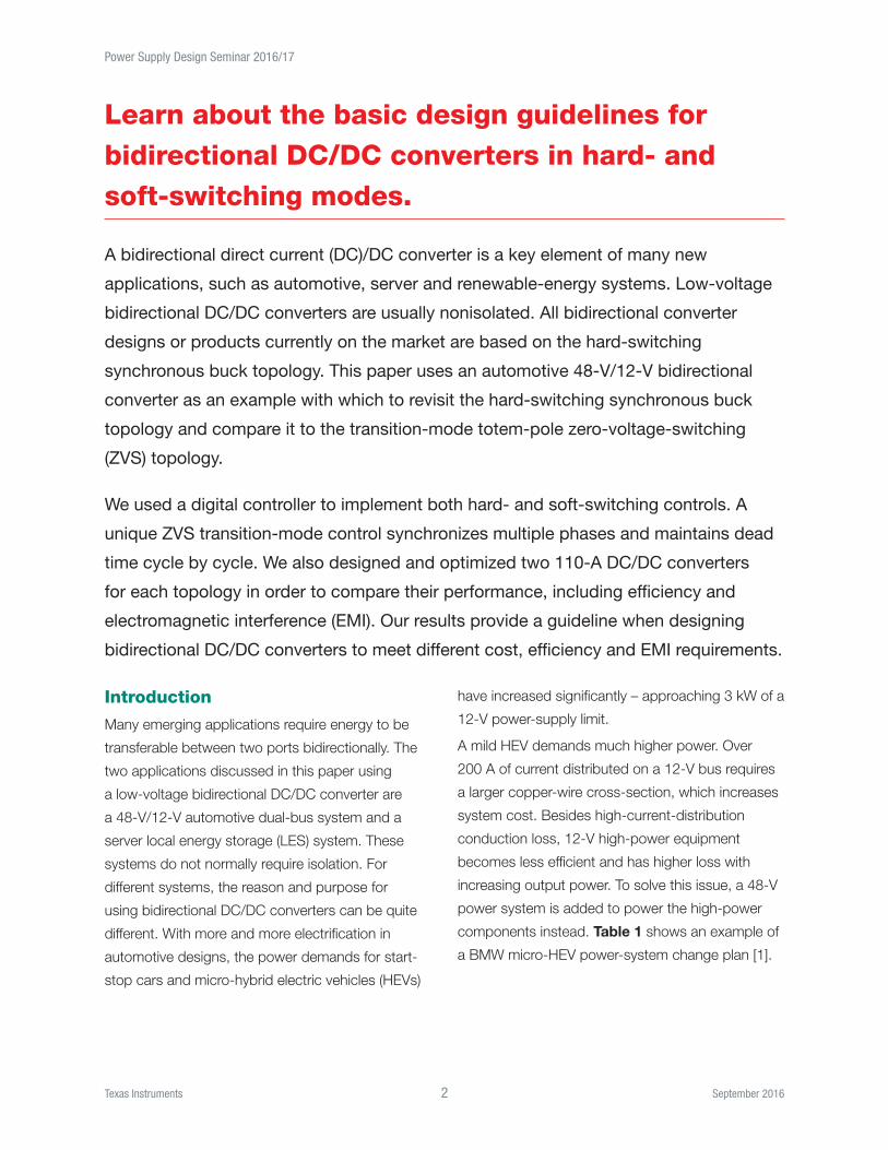
increasing output power. To solve this issue, a 48-V
power system is added to power the high-power
components instead. Table 1 shows an example of
a BMW micro-HEV power-system change plan [1].
Learn about the basic design guidelines for bidirectional DC/DC converters in hard- and soft-switching modes.
A bidirectional direct current (DC)/DC converter is a key element of many new
applications, such as automotive, server and renewable-energy systems. Low-voltage
bidirectional DC/DC converters are usually nonisolated. All bidirectional converter
designs or products currently on the market are based on the hard-switching
synchronous buck topology. This paper uses an automotive 48-V/12-V bidirectional
converter as an example with which to revisit the hard-switching synchronous buck
topology and compare it to the transition-mode totem-pole zero-voltage-switching
(ZVS) topology.
We used a digital controller to implement both hard- and soft-switching controls. A
unique ZVS transition-mode control synchronizes multiple phases and maintains dead
time cycle by cycle. We also designed and optimized two 110-A DC/DC converters
for each topology in order to compare their performance, including efficiency and
electromagnetic interference (EMI). Our results provide a guideline when designing
bidirectional DC/DC converters to meet different cost, efficiency and EMI requirements.
Texas Instruments 3 September 2016
Power Supply Design Seminar 2016/17
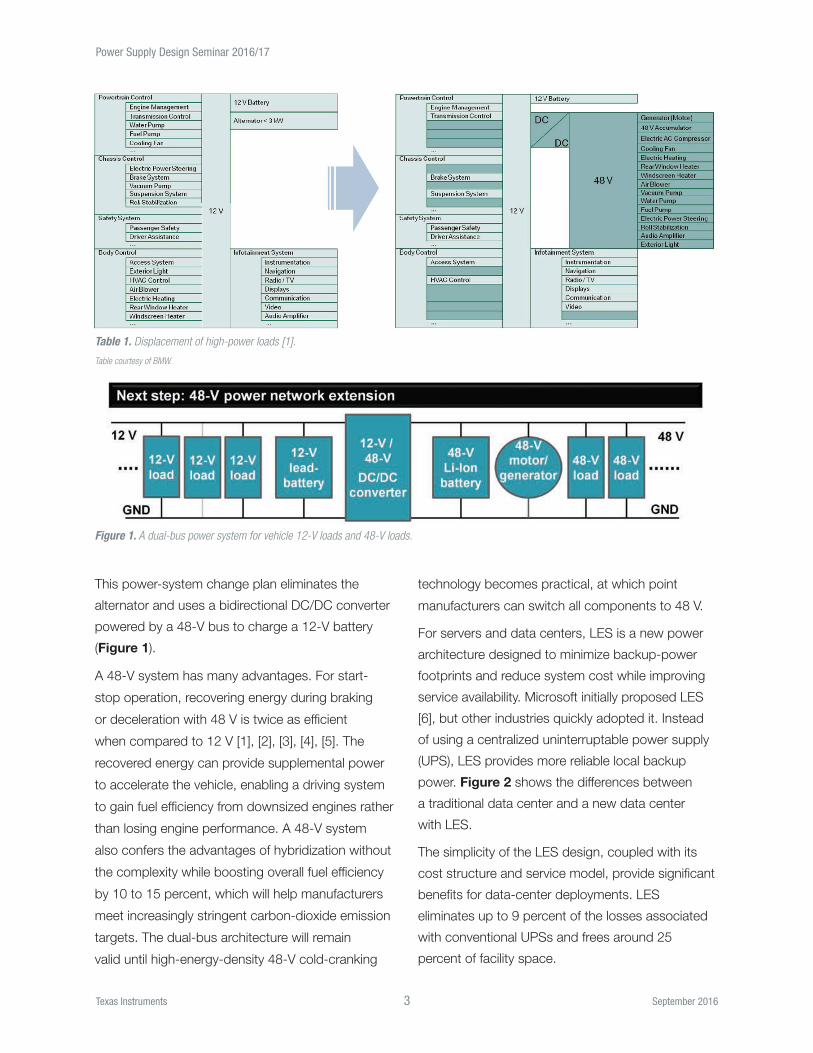
This power-system change plan eliminates the
alternator and uses a bidirectional DC/DC converter
powered by a 48-V bus to charge a 12-V battery
(Figure 1).
A 48-V system has many advantages. For start-
stop operation, recovering energy during braking
or deceleration with 48 V is twice as efficient
when compared to 12 V [1], [2], [3], [4], [5]. The
recovered energy can provide supplemental power
to accelerate the vehicle, enabling a driving system
to gain fuel efficiency from downsized engines rather
than losing engine performance. A 48-V system
also confers the advantages of hybridization without
the complexity while boosting overall fuel efficiency
by 10 to 15 percent, which will help manufacturers
meet increasingly stringent carbon-dioxide emission
targets. The dual-bus architecture will remain
valid until high-energy-density 48-V cold-cranking
technology becomes practical, at which point
manufacturers can switch all components to 48 V.
For servers and data centers, LES is a new power
architecture designed to minimize backup-power
footprints and reduce system cost while improving
service availability. Microsoft initially proposed LES
[6], but other industries quickly adopted it. Instead
of using a centralized uninterruptable power supply
(UPS), LES provides more reliable local backup
power. Figure 2 shows the differences between
a traditional data center and a new data center
with LES.
The simplicity of the LES design, coupled with its
cost structure and service model, provide significant
benefits for data-center deployments. LES
eliminates up to 9 percent of the losses associated
with conventional UPSs and frees around 25
percent of facility space.
Table 1. Displacement of high-power loads [1].
Table courtesy of BMW.
Figure 1. A dual-bus power system for vehicle 12-V loads and 48-V loads.

Texas Instruments 4 September 2016
Power Supply Design Seminar 2016/17
(a)
(b)
Figure 2. Traditional data center (a); Microsoft reinvented data center (b).
A bidirectional DC/DC converter is also a key
element of a server power supply with LES. When
powered by an alternating current (AC)/DC rectifier
output, a bidirectional DC/DC converter charges
LES batteries during normal operation. The LES
batteries provide backup power and regulate the
AC/DC rectifier output voltage in the event of a
power outage.
Bidirectional DC/DC converters have many
applications and play an increasingly important role in
energy recovery and power-system management. The
most popular topology used for a converter design
is a hard-switching synchronous buck converter, due
to its circuit and control simplicity [7]. The other main
topology is a ZVS transition-mode synchronous buck
converter. This topology can operate in ZVS mode
and has higher potential efficiency [8], [9], [10], [11].
Synchronous buck converters can operate in boost
mode when you reverse their output currents.
For automotive applications, a multiphase
interleaving structure avoids the need to use liquid
or air cooling, increases the converter’s power
capacity, and distributes heat dissipation across a
large area. Unlike a fixed-frequency hard-switching
interleaved synchronous buck converter, a ZVS
transition-mode interleaved buck converter operates
in frequency-modulation mode. You must control
its output inductor’s negative current to limit the
maximum switching frequency at light loads and
provide the necessary energy for ZVS operation at
heavy loads.
All phases must remain synchronized in any
operational situation. Optimal and reliable control is
complicated and still poses significant challenges
for converter designers. This paper focuses
on comparing the control implementation and
performance of the two different topologies. We
chose the UCD3138 digital controller for both hard-
switching and ZVS control, and designed a four-
phase 110-A/12-V power board to operate in both
hard-switching and ZVS modes.
Topology and control
A single-phase bidirectional converter (Figure 3)
can operate in buck mode and boost mode with
hard-switching or ZVS operation. When Q_top is an
active switch and Q_bot is a synchronous switch,
the converter operates in buck mode (Figure 4);
when the roles of Q_top and Q_bot reverse, the
converter is in boost mode (Figure 5).

Texas Instruments 5 September 2016
Power Supply Design Seminar 2016/17
Figure 3. A bidirectional converter power stage.
Figure 4. Waveforms in hard-switching buck mode.
Figure 5. Waveforms in hard-switching boost mode.
You can control the same buck converter to
achieve ZVS by letting the inductor current become
negative. When Q_top turns on in buck mode
(Figure 6), the inductor current, IL, builds up linearly.
When Q_top turns off, IL discharges switching node
V_SN down. As long as the dead time Td_off is
long enough, the bottom field-effect transistor (FET)
Q_bot is able to achieve ZVS. However, excessive
dead time results in a Q_bot body-diode conduction
loss increase. Thus, turn on Q_bot as soon as V_SN
discharges to zero.
Figure 6. Waveforms in ZVS buck mode.
Adaptive dead-time control minimizes switching
and body-diode conduction losses. Equation 1
calculates the dead time Td_off as:
(1)
where Coss_tr is the equivalent capacitance of a
metal-oxide semiconductor field-effect transistor
(MOSFET) when Vds swings between 0 and V48,
V48 is the voltage on the 48-V bus, and I_pk is the
active switch Q_top turn-off current.
After Q_bot turns on, IL starts to decline. The switch
stays on until the current reaches the predetermined
negative current expressed as Equation 2:
(2)
where V12 is the voltage on the 12-V bus and
Td_on is the dead time between when Q_bot turns
off and Q_top turns on.
To achieve optimal operation, the dead time Td_on
should be half the switch-node resonant period
(Equation 3):
(3)
𝑇𝑇𝑇𝑇_𝑜𝑜𝑜𝑜𝑜𝑜 = 2 ∙ 𝐶𝐶𝐶𝐶𝐶𝐶𝐶𝐶_𝑡𝑡𝑡𝑡 ∙ 𝑉𝑉!"
𝐼𝐼_𝑝𝑝𝑝𝑝
𝐼𝐼_𝑛𝑛𝑛𝑛𝑛𝑛𝑛𝑛𝑛𝑛𝑛𝑛𝑛𝑛𝑛𝑛 = 2 ∙ 𝐶𝐶𝐶𝐶𝐶𝐶𝐶𝐶_𝑡𝑡𝑡𝑡 (𝑉𝑉!" – 2 ∙ 𝑉𝑉!")
𝑇𝑇𝑇𝑇_𝑜𝑜𝑜𝑜
𝑇𝑇𝑑𝑑!" = 𝜋𝜋 𝐿𝐿𝐿𝐿 ∙ 𝐶𝐶𝐶𝐶𝑠𝑠𝑠𝑠!"

Texas Instruments 6 September 2016
Power Supply Design Seminar 2016/17
The energy stored in the output inductor is then just
enough to charge the switch-node V_SN up to the
V48 bus voltage, and Q_top can turn on with ZVS.
ZVS operation is also possible when operating
in boost mode, as shown in Figure 7. The
same control ideas apply to the negative-current
calculation and dead-time control.
Figure 7. Waveforms in ZVS boost mode.
For a hard-switching bidirectional converter
operating in continuous conduction mode (CCM),
use adaptive dead-time Td_off control to achieve
optimal efficiency but keep Td_on as small as
possible.
Control implementation
The UCD3138 is a hybrid digital controller made
up of three hardware digital loops and an ARM7
microcontroller [12]. The three digital loops can
operate independently or in cascade mode. The
controller architecture maintains the precision and
high speed required for power processing while
providing flexible power management.
A bidirectional DC/DC converter requires three loop
controls. One is a current loop, and the other two
are the V48 voltage loop and the V12 voltage loop.
The controller’s structure and peripherals match this
bidirectional converter application perfectly.
Figure 8 shows a circuit block diagram of a
controller-based bidirectional DC/DC converter.
One controller has eight digital pulse-width
modulator (DPWM) outputs (four pairs), which can
control four phases simultaneously. A shunt resistor
senses each phase inductor current. All phase
currents are summed together and connected to
EADC0 for current-loop control.
Figure 8. Circuit block diagram of a bidirectional DC/DC converter.
The 12-V and 48-V bus voltages are sensed and
fed to EADC1 and EADC2 for voltage-loop control.
Two general-purpose PWMs (PWM0 and PWM1)
generate two programmable analog negative-
current references and connect to compactor 1
and 2. One reference is for ZVS buck mode and
the other is for ZVS boost mode. The comparators
detect the master phase inductor’s negative current.
When the current reaches the reference threshold
values, the comparator output, which connects to
the UCD3138’s sync pin, becomes high.
The rising edge of the signal at synchronous input
forces the controller’s DPWM to restart a new
switching cycle and achieve hardware-based
frequency modulation. All slave phases follow the
master phase’s frequency cycle by cycle. Each slave
phase has a different delay time from the master
phase. The ARM7 can modify the delay time, so all
phases can maintain 90-degree interleaving when
the switching frequency varies.

Texas Instruments 7 September 2016
Power Supply Design Seminar 2016/17
One important feature of the UCD3138 is that
all dead times remain unchanged regardless of
switching-frequency changes, while the ARM7 still
has the privilege and flexibility to modify the dead
time at any point.
A bidirectional DC/DC converter benefits from
current-ripple cancellation of the interleaved
structure. Selecting the right phase number can
minimize or even fully cancel current ripple. For this
specific case, where the high-voltage bus is 48 V
and the low-voltage bus is 12 V, the voltage ratio is
4-to-1. The optimal phase number is thus a multiple
of four.
Figure 9 shows the normalized current ripple versus
the number of phases. You can see that for an ideal
case, the inductor current ripple fully cancels out
when the phase number is a multiple of four. It is for
this reason that we used a four-phase bidirectional
DC/DC converter to compare performance.
Figure 9. Current ripple versus the number of phases.
Design and test
To validate the control scheme and compare
topology performance, we designed a 110-A (on
the 12-V side) bidirectional DC/DC converter. When
loaded with a different set of power components,
the same design can operate in either hard-
switching mode or ZVS mode. Table 2 shows the
power-stage component selection and design, and
Figure 10 shows the 110-A bidirectional DC/DC
reference design.
Table 2. Power-stage component selection and design.

Texas Instruments 8 September 2016
Power Supply Design Seminar 2016/17
Figure 10. Example of a 110-A (1.6-kW) bidirectional DC/DC converter.
Figure 11 shows the switching-node voltage
waveforms and inductor current waveform when
the converter operates in ZVS buck mode. The
switching-node waveforms are clean and soft, with
a 90-degree phase offset from each other. The
maximum frequency is clamped to 450 kHz. As the
load decreases, the switching frequency increases.
When the switching frequency reaches the 450-kHz
limit, the negative current increases to prevent the
switching frequency from increasing further.
Figure 11. Switching-node voltage and inductor-current waveforms in ZVS buck mode.
Figures 12 through 19 show the difference
between hard switching and soft switching. ZVS
operation has softer voltage-rising and falling-edge
waveforms, but you can still see some voltage
overshoot when the MOSFETs turn off at a large
current due to the printed circuit board (PCB) and
power MOSFET pin leakage inductance. Hard-
switching operation has a higher voltage overshoot.
In addition to the PCB and MOSFET lead leakage,
the MOSFET body diode’s reverse recovery
contributes to overshoot and ringing as well.
Figure 12. Hard-switching buck at 20 A.
Figure 13. Soft-switching buck at 20 A.
Figure 14. Hard-switching buck at 110 A.
TI Information – Selective Disclosure. HVPS/ Battery Management Deep Dive 2015
Redefining the future of power through high voltage – www.TI.com/highvoltage Complete Solutions Robust Design Tools Innovative Products
Soft on/off edges
No overshoot
1-4
Fig 13

Texas Instruments 9 September 2016
Power Supply Design Seminar 2016/17
Figure 15. Soft-switching buck at 110 A.
Figure 16. Hard-switching boost at 20 A.
Figure 17. Soft-switching boost at 20 A.
Figure 18. Hard-switching boost at 110 A.
Figure 19. Soft-switching boost at 110 A.
Figure 20 shows the converter’s bidirectional
operation. The 12-V current ramps up and down
between positive and negative values. When
operating in buck mode, the current is positive and
charges the 12-V battery. The current becomes
negative in boost mode and the power from the
12-V battery charges up the 48-V battery.
Figure 20. Waveforms of bidirectional operation.

Texas Instruments 10 September 2016
Power Supply Design Seminar 2016/17
A graphical user interface (GUI) tool (Figure 21)
facilitates circuit debugging and tuning and handles
operation monitoring (Figure 22).
Figure 21. Device GUI for circuit debugging and tuning.
Figure 22. GUI for bidirectional DC/DC converter operation setting and monitoring.
We calculated the power losses of the reference
design and charted the losses in the columns
shown in Figure 23. You can see that the total loss
of the converter with ZVS operation reduces, but
the reduction is not significant. The major change
is the power loss shifting from the MOSFETs to
the inductors. This shift could be advantageous,
since magnetic components are more reliable than
semiconductors. Perhaps better magnetic materials
could improve the ZVS converter’s efficiency even
further. Figures 24 and 25 plot the converter’s
efficiencies versus loads.
Figure 23. Loss breakdown of hard-switching and ZVS buck converters at full load.
Figure 24. Efficiency versus load in buck mode.
Figure 25. Efficiency versus load in boost mode.
In both buck and boost mode, hard switching has
better light-load efficiency, while at heavy loads soft
switching becomes more efficient. Soft switching
still has turn-off loss. When the switching frequency
increases at light loads, the loss becomes more
significant.

Texas Instruments 11 September 2016
Power Supply Design Seminar 2016/17
We conducted additional tests with light-load
management, which showed that disabling the
synchronous FETs or using ideal diode-emulation
control improved efficiency substantially. This project
primarily focused on heavy loads where thermal
performance is the major concern, but real product
designs need light-load management.
Figures 26 through 29 show thermal images at
full loads. We did not use any forced air for cooling,
except a breeze from an electrostatic discharge
(ESD) ion generator on top of the test bench to help
stabilize the downfacing heat-sink temperature.
From the thermal images, you can see that the
MOSFETs’ soft-switching temperature is lower
than its hard-switching temperature in both buck
and boost modes, and the overall soft-switching
temperature is more even.
Figure 26. Hard-switching buck thermal image.
Figure 27. Soft-switching buck thermal image.
Figure 28. Hard-switching boost thermal image.
Figure 29.Soft-switching boost thermal image.
EMI is always one of the main concerns when
selecting a topology. To have a reasonable
comparison and better understand EMI behavior,
we used the same EMI filter design on both the
hard- and soft-switching converters and scanned
the EMI in buck mode at full load. Test data in
Figure 30 indicates that soft switching and hard
switching have no significant EMI difference under
1 MHz, but soft-switching’s advantages become
more substantial when the frequency increases.
At 10 MHz and above, soft switching results in as
much as a 15-dB reduction.

Texas Instruments 12 September 2016
Power Supply Design Seminar 2016/17
Summary and conclusions
We designed and optimized two 110-A bidirectional
DC/DC converters to compare performance in
hard and soft switching and developed a GUI to
facilitate circuit debugging, tuning and monitoring.
Soft switching had softer and smoother switching-
node waveforms and lower voltage overshoot. With
no light-load management, hard switching is more
efficient than soft switching at light loads, while soft
switching has better efficiency at heavy loads.
The efficiency advantage of soft switching at heavy
loads is not significant due to its large peak current
and high turn-off loss, but its shift of losses from
silicon to magnetic parts results in lower MOSFET
temperatures and more even thermal distribution
across the power board.
Light-load management can improve both soft-
and hard-switching light-load efficiency. Soft
switching does not exhibit a lower conducted
EMI emission under 1 MHz, but its advantage
becomes more significant with an increase in
frequency and reaches 15-dB EMI reductions
at 10 MHz and above.
Soft switching works better in general, but its
design and control are more challenging. Topology
selection for a design would depend on the specific
requirements and the time and resources available.
The UCD3138 was a good fit for both the hard-
and soft-switching bidirectional DC/DC converter
designs. Its hybrid architecture offers precise and
fast hardware power-processing control and flexible
software power management. The controller’s
hardware can support multiphase ZVS frequency
modulation and maintain a constant dead time.
Figure 30. Conducted EMI test of bidirectional DC/DC converters in buck mode at full load.

Texas Instruments 13 September 2016
Power Supply Design Seminar 2016/17
References
1. Sirch, O. “48 Volt – its threats and opportunities.”
Automotive 48 V Power Supply Systems 2013 International
Conference, Nov 12-14, 2013.
2. Harrop, P. “48 V vehicle systems becoming significant.”
IDTechEx, Aug. 12, 2015.
3. “48V: Collected facts, latest developments and expert
opinions.” Paper presented at 3rd International Conference
Automotive 48 V Power Supply Systems 2015,
Nov. 24-26, 2015.
4. “48V Technology on the Automotive Horizon.”
Automotive IQ report presented at the 3rd International
Conference Automotive 48 V Power Supply Systems 2015,
Nov. 24-26, 2015.
5. Els, P. “48 Volt Electrification: The next step to achieving
2020 emissions.” Paper presented at 3rd International
Conference Automotive 48 V Power Supply Systems 2015,
Nov. 24-26, 2015.
6. Harris, S. “Microsoft Reinvents Datacenter Power Backup
with New Open Compute Project Specification.” Microsoft
Server & Cloud Blog, March 10, 2015.
7. Waffler, S., and J.W. Kolar. “Efficiency Optimization of an
Automotive Multi-Phase Bi-directional DC-DC Converter.”
2009 IEEE 6th International Power Electronics and Motion
Control Conference (IPEMC 2009) 574-581.
8. Zhang, J. “Bidirectional DC-DC Power Converter Design
Optimization, Modeling and Control.” PhD diss, Virginia
Polytechnic Institute, 2008.
9. Liqin, N., D.J. Patterson, and J.L. Hudgins. “High Power
Current Sensorless Bidirectional 16-Phase Interleaved
DC-DC Converter for Hybrid Vehicle Application.” IEEE
Transactions on Power Electronics 27, No. 3 (2012)
1141-1151.
10. Yu, W., and J.S. Lai. “Ultra High Efficiency Bidirectional
DC-DC Converter with Multi-Frequency Pulse Width
Modulation.” Twenty-Third Annual IEEE Applied Power
Electronics Conference and Exposition (APEC) (2008)
1079-1084.
11. Sah, A., K. Chaudhary, and V.V. Ratnam. “Non-Isolated
Multiphase Buck-Boost Converter Design for Electric
Vehicle Applications.” 2014 Annual International
Conference on Emerging Research Areas: Magnetics,
Machines and Drives (AICERA/iCMMD) (2014) 1-6.
12. UCD3138 Highly Integrated Digital Controller for Isolated
Power. Texas Instruments data sheet (SLUSAP2F),
November 2013

TI Worldwide Technical Support
InternetTI Semiconductor Product Information Center Home Pagesupport.ti.com
TI E2E™ Community Home Pagee2e.ti.com
Product Information CentersAmericas Phone +1(512) 434-1560
Brazil Phone 0800-891-2616
Mexico Phone 0800-670-7544
Fax +1(972) 927-6377 Internet/Email support.ti.com/sc/pic/americas.htm
Europe, Middle East, and AfricaPhone European Free Call 00800-ASK-TEXAS (00800 275 83927) International +49 (0) 8161 80 2121 Russian Support +7 (4) 95 98 10 701
Note: The European Free Call (Toll Free) number is not active in all countries. If you have technical difficulty calling the free call number, please use the international number above.
Fax +(49) (0) 8161 80 2045Internet www.ti.com/asktexasDirect Email [email protected]
JapanFax International +81-3-3344-5317 Domestic 0120-81-0036
Internet/Email International support.ti.com/sc/pic/japan.htm Domestic www.tij.co.jp/pic
AsiaPhone Toll-Free Number Note: Toll-free numbers may not support
mobile and IP phones. Australia 1-800-999-084 China 800-820-8682 Hong Kong 800-96-5941 India 000-800-100-8888 Indonesia 001-803-8861-1006 Korea 080-551-2804 Malaysia 1-800-80-3973 New Zealand 0800-446-934 Philippines 1-800-765-7404 Singapore 800-886-1028 Taiwan 0800-006800 Thailand 001-800-886-0010International +86-21-23073444Fax +86-21-23073686Email [email protected] or [email protected] support.ti.com/sc/pic/asia.htm
A021014
Important Notice: The products and services of Texas Instruments Incorporated and its subsidiaries described herein are sold subject to TI’s standard terms and conditions of sale. Customers are advised to obtain the most current and complete information about TI products and services before placing orders. TI assumes no liability for applications assistance, customer’s applications or product designs, software performance, or infringement of patents. The publication of information regarding any other company’s products or services does not constitute TI’s approval, warranty or endorsement thereof.
© 2016 Texas Instruments IncorporatedPrinted in U.S.A. by (Printer, City, State) SLUP342
The platform bar and E2E are trademarks of Texas Instruments. All other trademarks are the property of their respective owners.

IMPORTANT NOTICE
Texas Instruments Incorporated and its subsidiaries (TI) reserve the right to make corrections, enhancements, improvements and otherchanges to its semiconductor products and services per JESD46, latest issue, and to discontinue any product or service per JESD48, latestissue. Buyers should obtain the latest relevant information before placing orders and should verify that such information is current andcomplete. All semiconductor products (also referred to herein as “components”) are sold subject to TI’s terms and conditions of salesupplied at the time of order acknowledgment.TI warrants performance of its components to the specifications applicable at the time of sale, in accordance with the warranty in TI’s termsand conditions of sale of semiconductor products. Testing and other quality control techniques are used to the extent TI deems necessaryto support this warranty. Except where mandated by applicable law, testing of all parameters of each component is not necessarilyperformed.TI assumes no liability for applications assistance or the design of Buyers’ products. Buyers are responsible for their products andapplications using TI components. To minimize the risks associated with Buyers’ products and applications, Buyers should provideadequate design and operating safeguards.TI does not warrant or represent that any license, either express or implied, is granted under any patent right, copyright, mask work right, orother intellectual property right relating to any combination, machine, or process in which TI components or services are used. Informationpublished by TI regarding third-party products or services does not constitute a license to use such products or services or a warranty orendorsement thereof. Use of such information may require a license from a third party under the patents or other intellectual property of thethird party, or a license from TI under the patents or other intellectual property of TI.Reproduction of significant portions of TI information in TI data books or data sheets is permissible only if reproduction is without alterationand is accompanied by all associated warranties, conditions, limitations, and notices. TI is not responsible or liable for such altereddocumentation. Information of third parties may be subject to additional restrictions.Resale of TI components or services with statements different from or beyond the parameters stated by TI for that component or servicevoids all express and any implied warranties for the associated TI component or service and is an unfair and deceptive business practice.TI is not responsible or liable for any such statements.Buyer acknowledges and agrees that it is solely responsible for compliance with all legal, regulatory and safety-related requirementsconcerning its products, and any use of TI components in its applications, notwithstanding any applications-related information or supportthat may be provided by TI. Buyer represents and agrees that it has all the necessary expertise to create and implement safeguards whichanticipate dangerous consequences of failures, monitor failures and their consequences, lessen the likelihood of failures that might causeharm and take appropriate remedial actions. Buyer will fully indemnify TI and its representatives against any damages arising out of the useof any TI components in safety-critical applications.In some cases, TI components may be promoted specifically to facilitate safety-related applications. With such components, TI’s goal is tohelp enable customers to design and create their own end-product solutions that meet applicable functional safety standards andrequirements. Nonetheless, such components are subject to these terms.No TI components are authorized for use in FDA Class III (or similar life-critical medical equipment) unless authorized officers of the partieshave executed a special agreement specifically governing such use.Only those TI components which TI has specifically designated as military grade or “enhanced plastic” are designed and intended for use inmilitary/aerospace applications or environments. Buyer acknowledges and agrees that any military or aerospace use of TI componentswhich have not been so designated is solely at the Buyer's risk, and that Buyer is solely responsible for compliance with all legal andregulatory requirements in connection with such use.TI has specifically designated certain components as meeting ISO/TS16949 requirements, mainly for automotive use. In any case of use ofnon-designated products, TI will not be responsible for any failure to meet ISO/TS16949.
Products ApplicationsAudio www.ti.com/audio Automotive and Transportation www.ti.com/automotiveAmplifiers amplifier.ti.com Communications and Telecom www.ti.com/communicationsData Converters dataconverter.ti.com Computers and Peripherals www.ti.com/computersDLP® Products www.dlp.com Consumer Electronics www.ti.com/consumer-appsDSP dsp.ti.com Energy and Lighting www.ti.com/energyClocks and Timers www.ti.com/clocks Industrial www.ti.com/industrialInterface interface.ti.com Medical www.ti.com/medicalLogic logic.ti.com Security www.ti.com/securityPower Mgmt power.ti.com Space, Avionics and Defense www.ti.com/space-avionics-defenseMicrocontrollers microcontroller.ti.com Video and Imaging www.ti.com/videoRFID www.ti-rfid.comOMAP Applications Processors www.ti.com/omap TI E2E Community e2e.ti.comWireless Connectivity www.ti.com/wirelessconnectivity
Mailing Address: Texas Instruments, Post Office Box 655303, Dallas, Texas 75265Copyright © 2016, Texas Instruments Incorporated