‘augmented feedback error correction’ (afec) for audio...
TRANSCRIPT

Andrew C. Russell
December 2012
(Updated September 2014)
‘Augmented Feedback Error Correction’ (AFEC) for Audio Amplifiers
AFEC is a simple technique that augments the feedback of a low
OLG CFA topology amplifier to dramatically improve the Large
Signal Non-linearity (LSN) distortion performance by up to 20 dB
across the audio band. Additionally, AFEC acts to remove any DC
offsets and also improve PSRR significantly.
Augmenting the feedback in a manner similar to that described
in this document has been tried previously – the first example is
from the early 1980’s at Hitachi. However, the technique never
entered the mainstream – one can only postulate that lack of
very high performance opamps (bandwidth, SR and distortion
performance), along with the difficultly of being able to
characterize such a system for stability modeling purposes (as we
can do now on LTspice for example) were contributing factors to
its early demise. However, as of 2014, these problems are now
solved, so perhaps we shall now see the return of AFEC as a
viable distortion reduction technique.

‘Augmented Feedback Error Correction’ (AFEC) for Audio Amplifiers
www.hifisonix.com Page 2
1. Introduction
One of the advantages of CFA power amplifiers is their very high slew rates (200+ V/us is not
uncommon), but loop gains tend not to be as high as VFA topology designs. This is fine at low to
medium signal levels, where the very good front end linearity and wide loop gain bandwidths of
CFAs’ manifest as low distortion; however, at higher power output levels where the output
stage and TAS/TIS LSN starts make itself felt, CFA distortion is generally worse, and this is as a
direct result of the lower loop gains – note, I am talking here about minimalist CFA topology
designs similar in structure to that shown in Fig. 6. Cross over is the major type of distortion in
class AB amplifiers and there have been various schemes invented to deal with this over the
years – most relying on feed forward techniques (see Peter Walker’s Quad Current Dumping for
example, or Michael Renardson’s MJR7 design). AFEC does a good job of reducing cross over
distortion artifacts, and in particular, those arising from OPS bias current shifts, but it will not
compensate for an under biased OPS where there is a clear discontinuity in the crossover region.
CFA amplifier PSRR is lower than VFA. This usually necessitates a front end stage regulator - the
D1 and D2 Zener diodes in Fig. 6 - but even then, the best designs are still usually 20~30 dB
below that of VFA exemplars. It will be shown that AFEC can improve CFA PSRR such that it
matches or exceeds VFA PSRR, whilst at the same time removing any output offsets as a result
of the servo action of the AFEC control amplifier.
2. The LSN Distortion Problem
In a conventional class AB power
amplifier, the biggest source of
distortion is as the output signal
transitions between the two halves
of the output stage. There is a
further major error term which is
directly linked to changes in the
output stage devices gain with load
current: LSN. Fig. 1 shows a plot of
output power and you can see the
characteristic form of this type of
distortion. This particular design has
an LF LG of c. 43 dB and at 20 kHz,
32 dB – quite typical figures. At
very low powers (so below about 1
W in this example) the amplifier is
running in class A and distortion is at
the low double digit PPM level; from about 4 W to 30 W the amplifier output stage linearity is
good and the distortion is essentially flat at about 50 PPM. Beyond this, the distortion starts to
increase as the output and TIS stage non-linearity increases due to loading effects. The available
Figure 1 – CFA EF2 Power Amplifier Distortion Profile (for 200W CFA design similar to Fig. 6 into 8 Ωs at 20 kHz)

‘Augmented Feedback Error Correction’ (AFEC) for Audio Amplifiers
www.hifisonix.com Page 3
loop gain from the amplifier in this example is fixed1 because the plot was done at 20 kHz, so it
is not the loop gain that is changing due to frequency changes – this shape correlates with
output stage and TIS non-linearity caused by increasing load.
The overall error (i.e. distortion) of this amplifier is small and in the PPM range compared to the
output power. This then leads to the question: Would it be possible to apply error correction to
augment the main feedback loop to lower the distortion and to remove as much as possible its
dependency upon output power?
3. Error Correction
Because of the assymptotic nature of distortion reduction in feedback2 amplifiers, very high
loop gains are required to get distotion down to ultra low levels – and here I am talking about
low single digit ppm across the audio band width. The solution is to see the main amplifer
feedback loop as simply needing some small amount of assistance in voltage or current terms to
pull it back into line – i.e. the departure from a perfect output is actually a small quanity error in
reality. Fig. 2 shows the basic concept. A more conventional approach to the problem, assuming
only U1 was being used in the conventional way without feedback augmentation, would be to
either raise U1’s open loop gain (OLG) amplifer or to linearize each of U1’s stages in local
feedback loops within a global feedback loop – i.e. a nested feedback loop structure, which it
has been shown elswhere to be the equivalent of raising the overall loop gain. Since what we
are proposing to do here is to augment the main feedback loop in some way, I have called this
technique augmented feedback error correction or AFEC for short - distortion reduction comes
about because the feedback factor is increased (augmented) by the control amplifer U2.
Figure 2 - AFEC concept diagram
1 Note that loop gain does changes due to loading as well, but this is much smaller than loop gain response changes due to compensation design. The -3 dB BW of the loop gain in an MC VFA is typically below a few hundred Hz, while in a classic CFA, it may be as high as 50~60 kHz 2 Error cancellation techniques fair better in theory because the error term is actually cancelled.

‘Augmented Feedback Error Correction’ (AFEC) for Audio Amplifiers
www.hifisonix.com Page 4
There have been many approaches over the years to try to improve the distortion performance
of audio amplifiers – some links to references are included in the back of this document, some
of them quite simple and elegant, others less so. AFEC’s attraction is that it is very simple –
adding only 1 dual op-amp, 3 precision resistors (R2, R3 and R6), some clamp diodes and a
compensation capacitor (not shown in Fig. 2 for clarity). U1 is a generic CFA topology power
amplifier (similar the one shown in Fig. 5), using conventional feedback with gain set by
[1+R2/R3]. The amplifier drives R1, a loudspeaker, with Rload 3~8 Ω3 over the audio bandwidth,
but even lower minimum impedances have been reported. A parallel feedback network
consisting of R4 and R5 - which must be in exactly the same ratio as R2:R3, senses the output
voltage Vo and feeds into the non-inverting input of U2, while the inverting input references the
input signal Vref after the input bandwidth limiting filter formed by R7 and C1. If the bridge
formed by R2, R4 and R3, R5 is well balanced (reasonably easy in practice with a bit of care) and
U2 is a fast, high performance, high open loop gain op-amp like an LM4562 or similar, then any
difference between the input signal (Vref) and Vo - an error term - will be amplified by the AFEC
amplifier U2. This output of U2 is then fed into the feedback node, the inverting input of U1, as
an error correction signal. R6, through which the error correction current is injected into the
summing node at the junction of R2 and R3, is selected to give the lowest distortion at Vo,
carefully considering the stability requirements – a subject to which we will return a bit later on.
In simulation, I found a value between 150 to 220 Ωs consistently delivered between 15 and 20
dB distortion reduction at 20 kHz, and improvements (using a LT1056) right up to about 80kHz
were clearly evident. The higher the value of R6, the lower the error correction current and the
lower the AFEC loop gain, leading to less output distortion reduction at Vo. Set R6 too low, and
when the amplifier clips there are large amounts of overhang and a tendency to oscillate as the
system exits overdrive – there are limits of course to how much feedback can be applied in any
system – this will be covered in section 7 where some guidelines are proposed.
For the scheme to work reliably, U2’s small signal performance in absolute terms really needs to
be better than U1 – if its not, it will actually contribute distortion at low input signal levels,
which of course has to be avoided. Secondly, the bandwidth and phase response of U2 should
be such that it does not lead to any overshoot or ringing, so ideally the small signal response of
U2 should be significantly better than U1, with C11 (Fig. 3) providing the necessary AFEC
amplifier loop compensation. Even though U1 is a CFA topology amplifier, a good VFA opamp
used in the U2 position and operating in its small signal region (which is the case in this design)
will generally be fast enough. Finally, when the system is overdriven, U2 has to recover very
quickly and without any sticky rail overhang – this can be accomplished with clamps as shown in
Fig. 3. Of course, it goes without saying that U2 should have adequate open loop gain as well.
It is important that the bridge (R2, R3 + R4, R5 in Fig. 2) is accurately balanced across the entire
system bandwidth. For this reason, these resistors should be co-located and any stray capacitive
coupling to surrounding circuits minimized. If the ratios are not well matched, this will manifest
3 See http://www.stereophile.com/content/real-life-measurements-page-2 and Keith Howard’s excellent expose here http://www.stereophile.com/reference/707heavy/

‘Augmented Feedback Error Correction’ (AFEC) for Audio Amplifiers
www.hifisonix.com Page 5
as a gain error – not an issue if it is steady state, but any dynamic mismatches due to
asymmetrical capacitive coupling, trace inductances or thermal effects, will result in additional
distortion terms.
The input filter formed by R7 and C1 is an important part of the overall system. It is always
advisable to limit the input signal bandwidth of a power amplifier – both to reduce unwanted
RFI and limit the input signal rise times to ensure SID cannot occur (a concern in VFA amplifiers
that has to be addressed through careful compensation design and input BW limiting4 and less
of an issue in CFA designs). In an AFEC equipped design, the input bandwidth and rise time must
be limited so excessive overshoot introduced by the control amplifier U2 in Fig. 2 does not occur,
and to ensure the system does not try to correct errors outside of its bandwidth capability. If
the AFEC amp introduces any overshoot, this will make the dynamic distortion of the overall
system worse.
Figure 3 - A Practical AFEC Control Amplifier Circuit. The +-15 V rails to power the opamp are derived from the CFA front end regulator circuit
Figure 3 details a practical circuit that was developed on LTSpice to test out the concept. Firstly,
since the input Vin is fed from after the amplifier input filter, any modulation of this node as
would be the case if Fig. 1 were implemented in a practical amplifier, would result in distortion.
Under normal operating conditions, this comes about due to the diode capacitance of the D3-D8,
clamp and any changes in U1’s input bias currents – a small effect in a JFET amplifier, but
significantly worse on some popular bipolar input opamps. The solution is to buffer the input
(U2 in Fig. 3) from the filter (R7 and C1 in Fig. 1) before feeding the actual error correction
amplifier U1 in Fig. 3 above. The AFEC control amplifier’s contribution to overall loop gain can be
reduced if necessary by placing a resistor across C11. In the Fig 6. design, I used 100k (R57), and
found values between 100k and 1MEG gave satisfactory results.
4 See the Ovation e-Amp write up for a detailed explanation of the design process in a VFA amplifier that addresses this type of distortion
Lowest distortion
coincides with
lowest voltage at Vb
Trim R75/R76
for null at Vb
for best
distortion
reduction
‘Augmented Feedback Error Correction’ (AFEC) for Audio Amplifiers
www.hifisonix.com Page 6
4. About the Amplifier Design Used in this Discussion
The overall system design shown in Fig. 6 is a development of the 100 W CFA nx-Amplifier
topology, with increased supply rails, additional OP transistors and is rated at 200W into 8 Ωs.
Above 100W, I would usually recommend that an EF3 OPS is considered, because the peak
output load currents on EF2 designs begin to affect the performance of the TIS through loading,
and distortion is much higher. However, here I have elected to stay with the EF2, as it is a very
useful vehicle for demonstrating the distortion reduction effected by AFEC. Simulations with an
EF3 showed that distortion of this design without AFEC was below 30ppm at 20 kHz, and with
AFEC engaged, around 3~5ppm - all figures at 200W into 8 Ωs. The slew rate without AFEC and
with the front end filter disabled is in the region of 200 V/us and with AFEC enabled and the
amplifier fully compensated 80 V/us; the -3 dB BW with filters and AFEC enabled is 600 kHz –
the upper BW figure can be tailored by adjusting the input filter (R10 and C1) values.
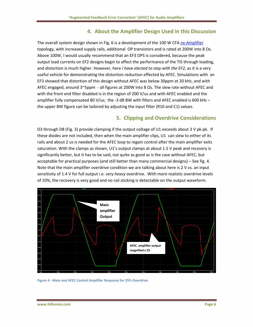
5. Clipping and Overdrive Considerations
D3 through D8 (Fig. 3) provide clamping if the output voltage of U1 exceeds about 3 V pk-pk. If
these diodes are not included, then when the main amplifier clips, U1 can slew to either of its
rails and about 2 us is needed for the AFEC loop to regain control after the main amplifier exits
saturation. With the clamps as shown, U1’s output clamps at about 1.5 V peak and recovery is
significantly better, but it has to be said, not quite as good as is the case without AFEC, but
acceptable for practical purposes (and still better than many commercial designs) – See fig. 4.
Note that the main amplifier overdrive condition we are talking about here is 2 V vs. an input
sensitivity of 1.4 V for full output i.e. very heavy overdrive. With more realistic overdrive levels
of 10%, the recovery is very good and no rail sticking is detectable on the output waveform.
Figure 4 - Main and AFEC Control Amplifier Response for 25% Overdrive
AFEC amplifier output
magnified x 25
Main
amplifier
Output
‘Augmented Feedback Error Correction’ (AFEC) for Audio Amplifiers
www.hifisonix.com Page 7
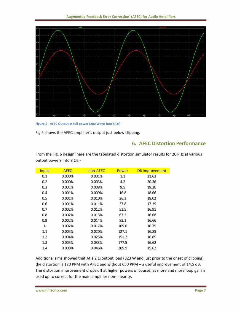
Figure 5 - AFEC Output at full power (200 Watts into 8 Ωs)
Fig 5 shows the AFEC amplifier’s output just below clipping.
6. AFEC Distortion Performance
From the Fig. 6 design, here are the tabulated distortion simulator results for 20 kHz at various
output powers into 8 Ωs:-
Additional sims showed that At a 2 Ω output load (823 W and just prior to the onset of clipping)
the distortion is 120 PPM with AFEC and without 650 PPM – a useful improvement of 14.5 dB.
The distortion improvement drops off at higher powers of course, as more and more loop gain is
used up to correct for the main amplifier non-linearity.
Input AFEC non-AFEC Power DB Improvement
0.1 0.000% 0.001% 1.1 21.63
0.2 0.000% 0.003% 4.2 20.36
0.3 0.001% 0.008% 9.5 19.30
0.4 0.001% 0.009% 16.8 18.66
0.5 0.001% 0.010% 26.3 18.02
0.6 0.001% 0.011% 37.8 17.39
0.7 0.002% 0.012% 51.5 16.91
0.8 0.002% 0.013% 67.2 16.68
0.9 0.002% 0.014% 85.1 16.66
1 0.002% 0.017% 105.0 16.75
1.1 0.003% 0.020% 127.1 16.85
1.2 0.004% 0.025% 151.2 16.85
1.3 0.005% 0.033% 177.5 16.62
1.4 0.008% 0.046% 205.9 15.62

‘Augmented Feedback Error Correction’ (AFEC) for Audio Amplifiers
www.hifisonix.com Page 8
Figure 6 – 200 W RMS CFA Amplifier Employing AFEC

‘Augmented Feedback Error Correction’ (AFEC) for Audio Amplifiers
www.hifisonix.com Page 9
In the sims I used an LT1057 high speed JFET input op-amp that was available in the LTSpice
library. A more thoroughly worked practical design would use something better like an
LME4562 and probably run the EC amp in class A for that last touch of refinement.
Figure 7 - AFEC Distortion Improvement Performance into 8 Ωs
Fig. 7 details the LTspice
simulation results for the Fig.
6 design into 8 Ωs, with the
purple line showing the dB
improvement of AFEC,
while Fig. 8 zooms in on just
the amplifier distortion with
AFEC active (8 Ω 20 kHz).
In Fig. 7, the reduction in
distortion effected by AFEC
is above 15 dB all the way
up to 205 W. The standard
feedback configuration, as
can be seen in Fig. 7, shows
distortion increasing from
70 ppm at ~10 W to double
that at 65 W output and 450
ppm at 205 W output. By
contrast, when AFEC is
engaged, distortion remains
below 50 ppm right up to
about 175 W, and thereafter
peaking at about 75 ppm at
205 W. Below 100 W, with
AFEC engaged, distortion is
under 25 ppm. It’s clear
from the shape of these
curves, and the absolute
value of the distortion, that
AFEC is very effective at
compensating for LSN. Importantly, AFEC is simple and the additional complexities of a high loop
gain amplifier are avoided - buffered TIS stages and EF3 being just two examples.
Fig. 9 shows the amplifier performance into 2 Ω. 2 Ω is an exceptionally heavy load, and usually
Figure 8 - Distortion performance only of AFEC equipped amplifier

‘Augmented Feedback Error Correction’ (AFEC) for Audio Amplifiers
www.hifisonix.com Page 10
Figure 9 - AFEC Performance into 2 Ω Load
only occurs around a few hundred Hz in a speakers impedance between the bass resonance and
the inevitable increase at HF due the crossover and wiring inductances – 3 Ω5 being a rather
more normal minima. However, I’ve done this to demonstrate the ameliorative effects of AFEC
even under extreme drive conditions. In Fig. 9 the 2 Ω load performance improvement across all
power levels from 0 W up to 823 W demonstrates a reduction in distortion >15 dB. Above 823
W, the main amplifier non-linearity starts rising quickly and the AFEC amplifier clamps, and all
distortion reduction comes to an abrupt halt. Recall that the AFEC control amplifier clamp
voltage was set to 1.5 V peak and was a compromise between distortion reduction and recovery
time from clipping. We could raise the clamp voltage to provide a little more headroom, but we
would then need to consider the recovery time from clipping under heavy load and overdrive
conditions – for now, the 1.5 V peak capability is a good compromise.
5 Of course, electrostatics present the worst load of all – see the Final speaker in Keith Howard’s Stereophile article referred to earlier for an extreme example.

‘Augmented Feedback Error Correction’ (AFEC) for Audio Amplifiers
www.hifisonix.com Page 11
Figure 10 – 2 Ω and 8 Ω Distortion Compared (20 kHz)
Fig 10 compares the distortion at both 2 and 8 Ωs. Since the power is 4 x higher on the 2 Ω load,
I plotted distortion vs Vo, rather than power. The green trace is the performance into 2 Ωs, and
the red trace for 8 Ωs. At 2 Ωs, the distortion ~4x the 8 Ω level. Interestingly, the distortion
remains essentially flat, varying little more than 2:1 around the 35 V output mark up until the
onset of clipping. The AFEC amplifier clamps on the 2 Ω load condition with 1.5 V input –in this
plot, I removed to last data point, as we see in Fig 9, to enable closer examination of the
performance at lower powers below the clamping point. It should be highlighted again, that this
performance is with an EF2 OPS – without AFEC, an EF3 is mandated for these levels of
performance, along with the additional circuit complexity required to deal with potential
instability issues.
2 Ω Load
8 Ω Load
175 W
700 W

‘Augmented Feedback Error Correction’ (AFEC) for Audio Amplifiers
www.hifisonix.com Page 12
7. AFEC Amplifier Loop Gain Considerations
Fig. 11 below shows the loop gain plot for the Fig. 6 amplifier. The green and dark blue traces
are for a 2 Ω load, and the red and light blue traces for the 8 Ω load condition.
Figure 11 - Loop gain for Fig. 5 amplifier with and without AFEC engaged into both a 2 Ω and 8 Ω load
The lower two blue traces show the amplifier loop gain without AFEC, and the top two with
AFEC engaged. At 20 kHz, AFEC adds about 30 dB of loop gain (both 2 Ω and 8 Ω cases). The 2
pole loop gain response is a result of combining the overall response of the main amplifier and
the AFEC control amplifier. Referring to Fig. 6, the AFEC and main amplifier response intersect
at a frequency determined by the value of R55 and the main amplifier feedback network R11
and R2, and is linked to the AFEC control amplifier loop gain response and the main amplifier
loop gain response. When R55 is reduced to a low value - say 22 Ω just by way of an example -
the loop gain increases up to as much as 120 dB and the gain intersect increases in frequency,
such that it falls above the ULGF, and the overall loop gain is no longer the classic 2 pole
response. Further, the phase margin under these conditions approaches 0 degrees – i.e. it is
unusable in a practical amplifier. On the other hand, high values for R55 (2.2k for example)
result in a very much lower overall loop gain – for 2.2k it is about 60 dB vs. 51 dB without AFEC
at LF - and results in a 2 pole loop gain response with an intersect frequency of ~100 kHz. The
overall effect in this case is that at 20 kHz the benefit is marginal and only provides 6 dB of loop
gain improvement. As discussed in Section 3, the overall system gain can be further tailored by
adjusting the value of R57. Without it, the full loop gain of the control amplifier is available for
error correction and the enhancement approaches 70 dB – I recommend values of between
100k and 1MEG which result in an LF loop gain enhancement of 30~50 dB, and at 20 kHz 25~30
dB.
Gain Intersect
Frequency

‘Augmented Feedback Error Correction’ (AFEC) for Audio Amplifiers
www.hifisonix.com Page 13
The conclusion to be drawn here is that AFEC should be set up such that there is 25 to 30 dB of
loop gain improvement at 20 kHz, and the overall loop gain is ~100 dB with a classic 2 pole
response and an intersect frequency between the main and AFEC control amplifiers of 500~700
kHz. This then leaves the final design with a 6~10x reduction in HF distortion depending on the
design specifics, 40+ degrees of phase margin, and the additional benefits of improved PSRR and
DC offset servo’ing. In the Fig 6 design, an additional point of note is the very high gain margin of
~35 dB which you can see in Fig. 11.
Many practitioners target phase margins of 45 degrees minimum, and I must admit, I usually
design for a minimum of 60 degrees. However, the use of an output inductor of 1 µH ensures
that this design can comfortably drive any capacitive load of up to 2 uF//2~8 Ωs and still remain
stable. 6
When investigating the overall loop gain in an AFEC equipped system, it is instructive to consider
the attenuation factors around the AFEC control amplifier. The AFEC loop gain is reduced by the
feedback factor (R4 and R5 in Fig. 2), and again by the feedback ratio around R6 and R3 (Fig. 2).
For a big amplifier, the gain is 32 dB, while if we consider the AFEC feedback as 220 Ω and the
main amplifier gain setting resistor at 15 Ω, we get 23 dB for a total of 55 dB. This will mean
that in an opamp with a 120 dB LF OLG used as an AFEC control amplifier, only about 65 dB will
be available to augment the main feedback loop – the cautionary notes about phase margin
covered previously notwithstanding.
Figure 12 - Small signal square wave response
6 It appears to have become fashionable over the last few years to not fit an output inductor - I do not subscribe to this approach.
See the Ovation e-Amp write-up for further details

‘Augmented Feedback Error Correction’ (AFEC) for Audio Amplifiers
www.hifisonix.com Page 14
Fig. 12 shows the small signal square wave response with the overall amplifier BW at the
previously quoted 600 kHz. The rise/fall times selected for this simulation were 100 ns (much
higher than would be found in any audio source signal where >2~3 µs is the norm) and the test
frequency 40 kHz. There is a small amount of overshoot and then recovery on the waveform
tops and bottoms. In a practical amplifier, you would compensate the main amplifier first by
adjusting the value of C3 (Fig. 6) for the best square wave response, then engage the AFEC
amplifier and secondly adjust C12 for the best square wave response. Finally, the input filter
network would then be further fine-tuned to optimize the square wave response. For the
simulation shown in Fig. 12, C12 was set for 22 pF. The overshoot can be reduced further, by
limiting the AFEC control amplifier bandwidth – but this has to be traded off for slew rate. I
experimented with up to 100pF for C12 without any stability issues.
Figure 13 - Large signal square wave performance
Fig. 13 demonstrates the large signal square wave response at 50 kHz. Slew rate is c. 80 V/us on a 40 V
pk-pk signal.

‘Augmented Feedback Error Correction’ (AFEC) for Audio Amplifiers
www.hifisonix.com Page 15
8. AFEC Drives Significant Improvements in PSRR
PSRR performance (See fig. 14) is a clear shortcoming in CFA amplifiers compared to VFA types.
But, AFEC provides a very neat way to improve CFA PSRR performance by upwards of 25 dB,
with simulation showing that an additional 30 dB can be achieved at frequencies below about 10
kHz. This then places CFA PSRR performance in the same league or better than conventional
VFA topology amplifiers. It does this because any PSRR error signals (read: unwanted output
signals) appearing at the output of U1 are suppressed by U2. Fig 14 shows the +Ve rail PSRR (the
–ve rail shows similar performance) improvement of about 30 dB, which is maintained up until
about 10 kHz.
Figure 14 - AFEC Improves CFA PSRR (green trace) by ~35dB below 10 kHz, and ~12 dB at 100 kHz. The blue trace shows PSRR performance of the Fig. 6 design with AFEC disabled
Further, since the design presented here is symmetrical, and the AFEC error correction is also
symmetrical, we get the same PSRR performance on both the negative and positive rails – a trick
‘blameless’ designs cannot pull off. Note that if there are large discrepancies in the control
opamp PSRR, this will of course result in small differences in the +ve and –ve PSRR – for the
most part however, the differences will be small enough not to be of concern. It must be
highlighted of course, that this aspect of AFEC is not a cure all for bad layout or sloppy designs.
As pointed out elsewhere, magnetic and common impedance coupling of unwanted signals and
so forth can quickly turn a fundamentally good design into something altogether pedestrian.
‘Augmented Feedback Error Correction’ (AFEC) for Audio Amplifiers
www.hifisonix.com Page 16
9. Conclusions and Observations
AFEC is a simple technique that provides asymptotic distortion reduction in class A and class AB
audio amplifiers of up to 20 dB at HF. The technique compares the input signal after a
bandwidth limiting filter to the output of the amplifier, magnifies any differences (since this
must be distortion and/or other extraneous signal(s)) and applies this to the amplifier negative
feedback node as an error correction signal. In simulation, the technique shows the promise of
reducing distortion by up to 20 dB at 20 kHz and across all power levels, while benefits up to 100
kHz are also evident. Depending on the compensation design specifics, distortion below ~5 kHz
can be reduced by up to 35 dB.
The approach is considerably simpler and easier to implement than some of the concepts
presented in the references at the end of this document – the Stochino and Quad Current
Dumping being two examples. AFEC specifically targets LSN and loading effects and it fairs less
well in gross cross over distortion reduction – which is what the Quad Current Dumping system
and Michael Renardson’s MFR7 amplifiers address. However, in an adequately biased output
stage, AFEC will also reduce the effects of changes in cross over distortion due to thermal effects
and my sims indicate that it will recover OPS under bias of up to 10%.
Further benefits of the approach presented are DC offset servo’ing (a byproduct of the AFEC
control amplifier DC performance) and improvements in PSRR of up to 35 dB below 10 kHz.
Above this frequency, PSRR improvements fall off, but the overall system is still better than
without AFEC engaged and easily equals or betters conventional ‘blameless’ VFA designs in this
regard.
Further work is needed to try the technique on VFA ‘blameless’ designs, where often a DC servo
is employed to avoid the feedback coupling capacitor7. By simply re-arranging the servo into the
AFEC configuration, the benefits described here may be brought to that topology as well.
Finally, AFEC can be added to any generic CFA amplifier for about $2 – most of which will be in
the expense of a good quality, low distortion opamp. This is considerably lower than the
additional drivers, small signal components and passives in conventional designs that achieve
the same results simply by raising the overall loop gain, to say nothing of the stability issues that
require careful characterization, assessment and mitigation.
7 Note that in the CFA design of Fig. 6, a DC servo is not actually required. In discrete form, the diamond input structure is very stable thermally, and once the initial offset is dialed out, the DC offset upon subsequent power-up cycles quickly settles to under 10 mV within a minute or two from an initial 40mV, and to 1~2mV within a few minutes after that. See the sx and nx amplifier for further discussion on this.

‘Augmented Feedback Error Correction’ (AFEC) for Audio Amplifiers
www.hifisonix.com Page 17
10. Useful links and References
1. Jan Diddens ‘Linear Audio’’ site discussing the pax-1 amplifier
2. Malcom Hawksfords papers on Output stage error Correction ‘Hawksford Error
Correction’ or HEC as it has become known and another paper here
3. Robert Cordell’s Mosfet amplifier incorporating HEC
4. Theory of Feedforward Amplifiers - some information from Italy
5. Michael Renardson The Renardson Feed Forward amplifier
6. Michael Renardson Distortion Measurement in Audio Amplifiers
7. Giovanni Stochino’s Feed Forward Audio Amplifier