atomic layer deposition of crystalline srhfo3 directly on
TRANSCRIPT

Atomic layer deposition of crystalline SrHfO3 directly on Ge (001) for high-k dielectricapplicationsMartin D. McDaniel, Chengqing Hu, Sirong Lu, Thong Q. Ngo, Agham Posadas, Aiting Jiang, David J. Smith,Edward T. Yu, Alexander A. Demkov, and John G. Ekerdt Citation: Journal of Applied Physics 117, 054101 (2015); doi: 10.1063/1.4906953 View online: http://dx.doi.org/10.1063/1.4906953 View Table of Contents: http://scitation.aip.org/content/aip/journal/jap/117/5?ver=pdfcov Published by the AIP Publishing Articles you may be interested in O 3 -based atomic layer deposition of hexagonal La 2 O 3 films on Si(100) and Ge(100) substrates J. Appl. Phys. 108, 084108 (2010); 10.1063/1.3499258 Atomic layer deposition of La x Zr 1 − x O 2 − δ ( x = 0.25 ) high- k dielectrics for advanced gate stacks Appl. Phys. Lett. 94, 053504 (2009); 10.1063/1.3075609 Improved electrical properties of Ge metal-oxide-semiconductor capacitor with HfTa-based gate dielectric byusing Ta O x N y interlayer Appl. Phys. Lett. 92, 262902 (2008); 10.1063/1.2954012 Suppressed growth of unstable low- k Ge O x interlayer in Ge metal-oxide-semiconductor capacitor with high- kgate dielectric by annealing in water vapor Appl. Phys. Lett. 90, 163502 (2007); 10.1063/1.2723074 Atomic layer deposition of gadolinium scandate films with high dielectric constant and low leakage current Appl. Phys. Lett. 89, 133512 (2006); 10.1063/1.2354423
[This article is copyrighted as indicated in the article. Reuse of AIP content is subject to the terms at: http://scitation.aip.org/termsconditions. Downloaded to ] IP:
129.116.140.202 On: Tue, 10 Feb 2015 16:46:16
Atomic layer deposition of crystalline SrHfO3 directly on Ge (001) for high-kdielectric applications
Martin D. McDaniel,1 Chengqing Hu,2 Sirong Lu,3 Thong Q. Ngo,1 Agham Posadas,4
Aiting Jiang,2 David J. Smith,3 Edward T. Yu,2 Alexander A. Demkov,4
and John G. Ekerdt1,a)
1Department of Chemical Engineering, The University of Texas at Austin, Austin, Texas 78712, USA2Microelectronics Research Center, The University of Texas at Austin, Austin, Texas 78758, USA3Department of Physics, Arizona State University, Tempe, Arizona 85287, USA4Department of Physics, The University of Texas at Austin, Austin, Texas 78712, USA
(Received 9 October 2014; accepted 17 January 2015; published online 3 February 2015)
The current work explores the crystalline perovskite oxide, strontium hafnate, as a potential high-kgate dielectric for Ge-based transistors. SrHfO3 (SHO) is grown directly on Ge by atomic layer
deposition and becomes crystalline with epitaxial registry after post-deposition vacuum annealing
at �700 �C for 5 min. The 2� 1 reconstructed, clean Ge (001) surface is a necessary template to
achieve crystalline films upon annealing. The SHO films exhibit excellent crystallinity, as shown
by x-ray diffraction and transmission electron microscopy. The SHO films have favorable elec-
tronic properties for consideration as a high-k gate dielectric on Ge, with satisfactory band offsets
(>2 eV), low leakage current (<10�5 A/cm2 at an applied field of 1 MV/cm) at an equivalent oxide
thickness of 1 nm, and a reasonable dielectric constant (k� 18). The interface trap density (Dit) is
estimated to be as low as �2� 1012 cm�2 eV�1 under the current growth and anneal conditions.
Some interfacial reaction is observed between SHO and Ge at temperatures above �650 �C, which
may contribute to increased Dit value. This study confirms the potential for crystalline oxides
grown directly on Ge by atomic layer deposition for advanced electronic applications. VC 2015AIP Publishing LLC. [http://dx.doi.org/10.1063/1.4906953]
I. INTRODUCTION
In the last decade, significant material changes to com-
plementary metal oxide semiconductor (CMOS) devices
have included the introduction of strained Si channels to
improve performance and efficiency and metal gate/high-kdielectric stacks to address leakage current issues.1–3 More
recently, there has been renewed interest in using Ge as a
channel material due to its higher hole (1900 vs. 500 cm2/V
s) and electron (3900 vs. 1400 cm2/V s) mobility compared
to Si.4–7 Crystalline oxides are also being considered by the
semiconductor industry as next-generation high-k dielec-
trics.8 For example, there is tremendous interest in epitaxial
integration of perovskite oxides, such as SrTiO3 (STO) or
BaTiO3 (BTO), on semiconductors due to their functional
properties and very high permittivities.9–12 One primary
advantage of crystalline, epitaxial dielectrics is the possibil-
ity of having virtually no defects in the bulk of the dielectric
or at the interface with the semiconductor in an ideal hetero-
epitaxial system. For practical realization of high-mobility
channels in CMOS technology, surface passivation of the
semiconductor substrate and a high-quality oxide-semicon-
ductor interface must be realized.
Integration of high-k dielectrics on germanium has been
studied by many groups,13–19 but the electrical performance
of Ge-based devices has been less than optimal. Several
methods have been employed to control the interface trap
density (Dit) in order to achieve high performance.15,16,18
Typical values reported for high-k/Ge gate stacks show
Dit� 1011–1012 cm�2 eV�1. However, crystalline oxides
have the potential to create a nearly perfect electrical inter-
face by drastically reducing the interface trap density
(Dit< 1010 cm�2 eV�1).19,20 For a material to be suitable as a
gate dielectric replacement, it needs to satisfy several
requirements, including high permittivity, sufficiently large
band gap and proper band alignment (with 1 eV offset to
both bands) to the semiconductor, thermodynamic stability,
good film morphology, and high interface quality. Materials
related to TiO2, including STO and BTO, have high permit-
tivities, but the conduction band offsets with Si and Ge are
very small to negligible.21–23 Alternatively, crystalline stron-
tium hafnate, SrHfO3 (SHO), meets many of the high-krequirements and has a reasonable lattice match to Ge
(�1.9% mismatch), making it an ideal material candidate for
Ge-based transistors.
There are relatively few reports on thin film deposition
of SHO to date.24–32 In some early work, crystalline SHO
was investigated as a future gate dielectric material for Si-
based devices.25,27 The SHO films were grown by molecular
beam epitaxy (MBE) on Si (001) despite the 6% lattice mis-
match. The electrical performance of epitaxial SHO on Si
showed low equivalent oxide thickness (EOT) of 0.7 nm and
low leakage current (10�6 A/cm2) at �1 V.25 However, the
relatively high Dit (�1013 eV�1cm�2) likely contributed to
the poor mobility of the SHO/Si field-effect transistors
(FETs), where both n-FETs and p-FETs exhibited carrier
mobilities of �25 cm2/V-s at 1 MV/cm.25 Later work showed
a)Author to whom correspondence should be addressed. Electronic mail:
0021-8979/2015/117(5)/054101/9/$30.00 VC 2015 AIP Publishing LLC117, 054101-1
JOURNAL OF APPLIED PHYSICS 117, 054101 (2015)
[This article is copyrighted as indicated in the article. Reuse of AIP content is subject to the terms at: http://scitation.aip.org/termsconditions. Downloaded to ] IP:
129.116.140.202 On: Tue, 10 Feb 2015 16:46:16

that the SHO films on Si lacked significant strain and con-
firmed the in-plane misalignment of grains, which can de-
grade mobility.30 The large lattice mismatch between SHO
and Si, and subsequent relaxation of the film, likely contrib-
uted to the formation of these undesirable defects.
For epitaxial SrHfO3 thin films, Ge is a more suitable
substrate than Si in terms of the lattice match. Cubic SHO
has a lattice constant of 4.069 A.33 The Ge (001) surface has
an in-plane atomic spacing of 3.992 A, which would lead to
compressive lattice strain in commensurate, epitaxial SHO
films of 1.9%. In addition to the closer lattice match, other
physical properties make crystalline SHO a good candidate
dielectric for Ge-based devices. Polycrystalline SHO films
are reported to have a dielectric constant up to k� 35,24,28
leading to an EOT of less than 0.6 nm with a 5 nm film using
the ratio of k/3.9. However, other studies have reported lower
dielectric constants (k� 20) for SHO,26,32 similar to the bi-
nary oxide HfO2. Finally, SHO has a large band gap of
6.1 eV with favorable conduction band offset (�2.2 eV) and
valence band offset (�3.2 eV) with Ge.26,34 This is in con-
trast with Ti-based perovskites, where the Ti 3d states yield
negligible conduction band offsets with Si and Ge
(�0.1–0.5 eV).21,22,35 A direct comparison between SHO
and STO films on Si (001) has shown a reduction in gate
leakage by 4 orders of magnitude for SHO versus STO.26
Recently, we reported the growth of single crystal STO
(a¼ 3.905 A) on Ge (001) by atomic layer deposition (ALD)
followed by post-deposition annealing in vacuum.23
Capacitor structures revealed a large dielectric constant
(k� 90) for the STO films, but a high leakage current of
�10 A/cm2 for an applied field of 0.7 MV/cm. To circum-
vent this leakage issue, we explore the Hf-based perovskite,
SHO, with optimal band alignments to Ge and associated
reduction in leakage current. As detailed in our previous
report,23 the controlled growth by ALD on a clean Ge (001)
surface enables a chemical route to epitaxial oxide integra-
tion with semiconductors. Here, we confirm this growth and
annealing protocol to realize crystalline SHO films, and eval-
uate the potential for epitaxial SHO films as a future gate
dielectric for Ge-based transistors.
II. EXPERIMENTAL
Strontium hafnate, SrHfO3 (SHO), thin films are depos-
ited by ALD at a substrate temperature of 225 �C using
strontium bis(triisopropylcyclopentadienyl) [Sr(iPr3Cp)2]
(HyperSr),36 hafnium formamidinate (Hf-FAMD),37 and
purified water as co-reactants. Both the Sr and Hf metalor-
ganic precursors are commercially available, reactive with
water, and have been previously used for ALD.38–48
Alternating subcycles of Sr and Hf are used to deposit stoi-
chiometric to slightly Sr-rich (56%) films. During each sub-
cycle the metalorganic is dosed for 2 s to ensure complete
saturation of the surface, and subsequently purged for 15 s
with ultrahigh purity Ar. The water co-reactant is dosed for
1 s followed by a 15 s Ar purge.
The Ge (001) substrate is prepared from a 4-inch Ge wa-
fer (Sb-doped, q� 0.04 X cm) from MTI Corp. The as-
received Ge wafer is diced into approximately 18� 20 mm2
sample pieces. The sample is degreased by placing the wafer
in ultrasonic baths of acetone, isopropyl alcohol, and water
for 10 min each. The sample is then dried with nitrogen and
exposed to ultraviolet/ozone for 30 min to remove residual
carbon contamination. The sample is then immediately
loaded into the load lock chamber and pumped by a turbo-
molecular pump to a vacuum below 5� 10�7 Torr before
transferring into the annealing chamber. The surface GeO2 is
removed by annealing the sample at 700 �C in vacuum
(<2� 10�9 Torr) for 1 hr. After thermal deoxidation, the Ge
substrate is brought to below 200 �C before transfer into the
ALD system. The heating and cooling rates are fixed at
20 �C min�1. The low base pressure of the annealing cham-
ber minimizes potential contamination of the Ge surface dur-
ing thermal deoxidation. The clean Ge (001) surface then
shows a sharp, intense 2� 1 reconstruction that is observed
by in situ reflection high-energy electron diffraction
(RHEED).
After achieving the 2� 1 reconstructed Ge surface, the
sample is transferred into the ALD chamber, with a base
pressure of 5� 10�7 Torr, and allowed at least 30 min to
reach thermal equilibrium. Ultrahigh purity argon is used as
the carrier/purge gas and maintains the deposition pressure at
1.0 Torr. To deposit stoichiometric to Sr-rich (�56%) films
of SHO, a subcycle ratio of 1:1 (Sr:Hf) is used. This is in
contrast to STO films, where the initial deposition on Ge
required a Sr-heavy subcycle ratio of 2:1 (Sr:Ti).23 Upon
deposition of the SHO film, the sample is transferred back
into the annealing chamber for crystallization. Post-
deposition annealing is carried in vacuum (<2� 10�9 Torr)
with a temperature ramp rate of 20 �C/min.
The SHO films were post-deposition annealed at a sub-
strate temperature of 650–850 �C. The transition of the films
from amorphous to crystalline is observed in real time by insitu RHEED. After crystallization, in situ x-ray photoelec-
tron spectroscopy (XPS) is used to check the chemical com-
position and oxidation states, as well as to measure the
valance band offset of the SHO-Ge heterostructure. XPS is
performed using a VG Scienta R3000 analyzer and a mono-
chromated Al Ka source at 1486.6 eV. The analyzer is cali-
brated using a silver foil, where the Ag 3d5/2 core level is
defined to be 368.28 eV and the Fermi level of Ag at
0.00 eV. High-resolution spectra of Sr (3d, 3p), Hf (4f, 4d5/
2), O 1s, C 1s, and Ge (3d, 2p3/2) core levels are measured
using a pass energy of 100 eV with an analyzer slit width of
0.4 mm, resulting in an effective resolution of 350 meV.
Each high-resolution scan is measured four times and
summed, using 50 meV steps with a dwell time of 157 ms
per step. Film composition is estimated using CasaXPS (ver-
sion 2.3.16) peak fitting with a Shirley background subtrac-
tion and relevant sensitivity factors.49
The epitaxial SHO films are characterized ex situ by x-
ray reflectivity (XRR), x-ray diffraction (XRD), and cross-
section transmission electron microscopy (TEM). XRR is
performed using a Rigaku Ultima IV equipped for thin-films
with automated alignment. XRD is performed using an
X’PERT Powder Diffractometer with a sealed tube Cu Karadiation (k� 1.5406 A). Cross-sectional TEM is performed
with a 400-keV high-resolution electron microscope (JEM-
054101-2 McDaniel et al. J. Appl. Phys. 117, 054101 (2015)
[This article is copyrighted as indicated in the article. Reuse of AIP content is subject to the terms at: http://scitation.aip.org/termsconditions. Downloaded to ] IP:
129.116.140.202 On: Tue, 10 Feb 2015 16:46:16

4000EX) equipped with a double-tilt specimen holder. The
samples are prepared using standard mechanical polishing
followed by argon-ion-milling to perforation.
Standard metal-oxide-semiconductor capacitor
(MOSCAP) structures are created for capacitance-voltage
(C-V) and current-voltage (I-V) measurements. The top elec-
trode on the oxide surface is formed using sputtering of TaN,
photolithography, and SF6-based plasma etching. The bot-
tom electrode is formed by using silver paste on the
scratched backside of the Ge substrate. Both C-V and I-V
were measured in air at room temperature under dark condi-
tions using an Agilent B1500A semiconductor device param-
eter analyzer with a Cascade Microtech probe station. The
sweeping voltage was applied to the top electrode with the
bottom electrode grounded. The density of interface traps
(Dit) was estimated using the conductance method with a
range of frequencies extending from 1 kHz to 1.2 MHz.50
III. RESULTS AND DISCUSSION
A. Deposition and crystallization of SrHfO3 on Ge
Strontium hafnate films were deposited by ALD on the
reconstructed Ge (001) at 225 �C. Film thicknesses between
1 and 20 nm were deposited, and the films were subsequently
crystallized in vacuum at temperatures greater than 650 �C(typically 700 �C). Some thicker SHO films (>5 nm) were
grown in a two-step growth and anneal process for compari-
son. Figure 1 shows a series of RHEED images for a 2-nm-
thick SHO deposition: (a) after thermal deoxidation of the
Ge (001) substrate showing a clear 2� 1 reconstructed sur-
face and (b) the amorphous SHO film after ALD and the
crystalline SHO film after post-deposition vacuum annealing
at 700 �C for 5 min, where the beam is aligned along the (c)
h100i and (d) h110i directions of the perovskite oxide. Four-
fold symmetry of the crystalline SHO film was observed by
rotating the sample under electron illumination.
In situ XPS analysis was used to check the SHO film
stoichiometry. High-resolution scans of the most prominent
core-levels, Sr 3d and Hf 4f, were used for compositional
analysis. Representative core-level spectra for a 2-nm-thick
SHO film are shown in Figure 2. Both the Sr 3d and Hf 4fchemical shifts shown in Figs. 2(a) and 2(b), respectively,
are consistent with the fully oxidized species (SrHfO3). The
fitted peak positions are located at binding energies of
134.0 eV and 135.7 eV for Sr 3d5/2 and Sr 3d3/2, respectively,
and 16.9 eV and 18.5 eV for Hf 4f7/2 and Hf 4f5/2, respec-
tively. The asymmetry observed on the high binding energy
side of the Hf 4f high-resolution scan is due to overlap of the
Sr 4p peak, at approximately 19.8 eV. Deconvolution of the
spectra allows for subtraction of the Sr 4p component and
appropriate estimation of the film stoichiometry. For the
sample shown in Fig. 2, the Sr:Hf ratio is 56:44. For the
growth of crystalline perovskite oxides, stoichiometric to
slightly Sr-rich is preferred due to the relative ease with
which additional SrO layers can be incorporated while main-
taining the film crystallinity. Previous work from our group
has shown that Sr-rich STO films maintain the perovskite
structure, while Ti-rich STO films are more likely to be
amorphous.46 The samples grown for this study varied
slightly in cation stoichiometry from 52% to 56% Sr.
XRD and rocking curve analyses were performed ex situto verify the crystalline structure and out-of-plane alignment,
as shown in Figure 3. Fig. 3(a) shows a rocking curve around
the SHO (002) peak for a 4.6-nm-thick SHO film, with a
full-width half-maximum of 1.2�. The SHO film was post-
deposition annealed in vacuum at a substrate temperature of
725 �C for 5 min. Fig. 3(b) shows a schematic model of the
cubic perovskite SrHfO3, where the bulk lattice constant is
4.069 A. Fig. 3(c) shows a h-2h scan of the 4.6 nm SHO film
FIG. 1. RHEED patterns for a 2-nm-
thick SrHfO3 deposition (a) after
thermal deoxidation of the Ge (001)
substrate showing a visible 2� 1
reconstructed surface, (b) the amor-
phous SrHfO3 film after ALD and the
crystalline SHO film after post-
deposition vacuum annealing at 700 �Cfor 5 min where the beam is aligned
along the (c) h100i and (d) h110i direc-
tions of SrHfO3.
FIG. 2. X-ray photoelectron spectra of a 2-nm-thick SrHfO3 film showing
the most prominent core-levels: (a) Sr 3d and (b) Hf 4f. Deconvolution of
the spectra (dashed lines) highlights the individual contributions of the Sr
and Hf core-levels to the overall intensity.
054101-3 McDaniel et al. J. Appl. Phys. 117, 054101 (2015)
[This article is copyrighted as indicated in the article. Reuse of AIP content is subject to the terms at: http://scitation.aip.org/termsconditions. Downloaded to ] IP:
129.116.140.202 On: Tue, 10 Feb 2015 16:46:16

on Ge, where only the (001)-oriented peaks are present. The
SHO (002) peak position, 44.35 6 0.05�, corresponds to an
experimental c-axis lattice spacing of 4.082 6 0.005 A for
the epitaxial film. This suggests that the c-axis is slightly
expanded from the bulk, consistent with compressive in-
plane strain. Assuming SHO (a� 4.069 A) is perfectly
strained to the Ge surface (3.992 A), and a Poisson ratio of
0.25,51 the expected out-of-plane lattice spacing would be
4.088 A. This suggests that the 4.6 nm SHO film is at least
partially strained to the underlying Ge substrate for the
growth and annealing conditions.
B. Band offset of the SrHfO3-Ge heterojunction
In situ XPS analysis was used to estimate the band offset
of the SHO-Ge heterojunction. Shallow core-level and va-
lence band spectra were collected for bulk Ge (001), 11.2-
nm-thick SHO (001) film grown by ALD, and the SHO-Ge
(001) heterojunction. The thick SHO film was grown in a
two-step growth and anneal process, with a measured stoi-
chiometric ratio of 54:46 (Sr:Hf). The Ge substrate was pre-
pared by solvent degreasing, UV/ozone exposure, and UHV
annealing (700 �C for 1 h) as described in Sec. II. Both core-
level and valence band spectra were collected using a mono-
chromated Al Ka source at 1486.6 eV. The valence band
spectra for both the clean Ge (001) substrate and the 11.2-
nm-thick SHO film are shown in Figure 4.
For the Ge (001) substrate, the energy difference
between the valence band edge and Ge 3d5/2 centroid was
29.30 6 0.05 eV. For the 11.2-nm-thick SHO film, the energy
difference between the valence band edge and the Hf 4f7/2
centroid was 13.26 6 0.05 eV. To probe the SHO-Ge
heterojunction, a thin (�2 nm) epitaxial SHO film was grown
on Ge. Both the Ge 3d and Hf 4f core-levels were measured,
where the energy difference between the Ge 3d5/2 and Hf
4f7/2 centroids was 12.77 6 0.05 eV. Using the measured
energy differences, the valence band offset (VBO) between
SHO and Ge was estimated to be �3.27 6 0.10 eV.
To calculate the conduction band offset (CBO), we
assume the bulk band gap values of SHO and Ge to be
6.1 eV and 0.66 eV, respectively.26,52 The resulting CBO is
2.17 6 0.10 eV, as shown schematically in Figure 5. The pos-
itive band offset value means the band energy is higher in
the epitaxial SHO film. It should be noted, however, that the
CBO may be overestimated due to the uncertainty in the
bulk SHO band gap value. In other work, the electronic band
gap for SHO has been reported to be 5.8 eV based on photo-
emission spectra and x-ray absorption data.31 Regardless, the
band alignment between crystalline SHO and Ge (001) is
well above the minimum �1 eV band offset required for suit-
able gate dielectrics.53
C. MOSCAP performance
Capacitor structures were made on five samples of vary-
ing SHO thickness to measure the capacitance of the oxide
FIG. 3. X-ray diffraction and rocking curve analysis of a 4.6-nm SrHfO3
film on Ge: (a) rocking curve around the SHO (002) peak, with a full-width
half-maximum of 1.2�, (b) schematic model of the cubic perovskite SrHfO3
(a� 4.069 A), and (c) h-2h scan of the 4.6-nm SHO film on Ge, where only
(001)-oriented peaks are present.
FIG. 4. Valence band spectra for both clean Ge (001) substrate (red squares)
and 11.2-nm-thick SrHfO3 film (blue circles).
FIG. 5. Band alignment of the SHO-Ge heterojunction estimated using shal-
low core-level and valence band spectra. The bulk band gap values of SHO
and Ge were taken to be 6.1 eV and 0.66 eV, resulting in a CBO of 2.17 eV
and VBO of �3.27 eV.
054101-4 McDaniel et al. J. Appl. Phys. 117, 054101 (2015)
[This article is copyrighted as indicated in the article. Reuse of AIP content is subject to the terms at: http://scitation.aip.org/termsconditions. Downloaded to ] IP:
129.116.140.202 On: Tue, 10 Feb 2015 16:46:16
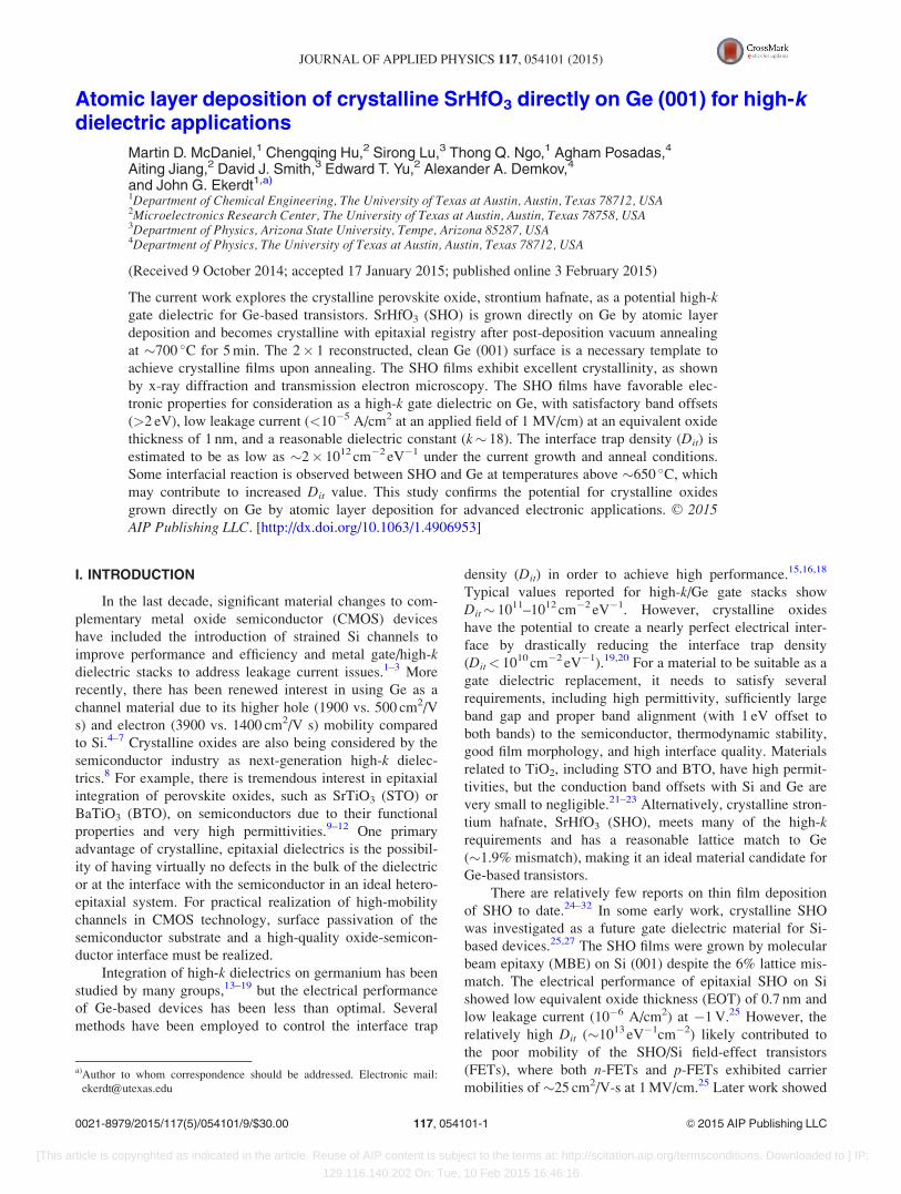
layer (Cox) and extract the dielectric constant. These data are
summarized in Figure 6 as a plot of capacitance equivalent
thickness (CET) versus physical thickness of the epitaxial
SHO layer. The dielectric constant is estimated to be k� 18
for crystalline SHO. This value is much lower than the
k� 35 that was reported previously for polycrystalline SHO
grown on TiN/Si substrates by MBE;24,28 however, it is con-
sistent with lower values reported for epitaxial SHO on Si
(k� 20) and polycrystalline SHO grown by plasma-assisted
ALD (k� 21).26,32 The high dielectric constant (k� 35) for
polycrystalline SHO was only achieved after post-deposition
annealing at 800 �C or higher on TiN/Si substrates,28 possi-
bly resulting in Ti diffusion into the SHO layer. It is there-
fore reasonable to conclude that the dielectric constant of
SHO is similar to that of the binary oxide HfO2 (k� 20).
To understand the effect of crystallization on the electri-
cal performance, a comparison was made between crystalline
and amorphous SHO films. Both SHO films were grown
directly on the 2� 1 reconstructed Ge surface with a nominal
thickness of 20 nm. The amorphous SHO film was not post-
deposition annealed, whereas the crystalline SHO film was
post-deposition annealed at 700 �C for 5 min in vacuum.
MOSCAP structures were formed for both the crystalline
and amorphous SHO samples. The amorphous SHO film
showed a much lower saturation capacitance (Cox) than the
crystalline SHO film. This results in an effective dielectric
constant of k� 12 for the amorphous SHO and k� 20 for the
crystalline SHO film. However, despite an increase in
dielectric constant, the observed Dit was significantly higher
for the crystalline film. Using the conductance method, the
Dit was estimated to be 2� 1012 cm�2 eV�1 and
4� 1013 cm�2 eV�1 for the amorphous and crystalline SHO
films, respectively. The increase of interface traps for the
crystalline film is cause for concern since one of the
expected benefits of epitaxial oxide dielectrics is the poten-
tial for drastically reduced interface traps. Additional studies
are needed to understand the origin of these interface trap
states in ALD-grown epitaxial dielectrics on Ge.
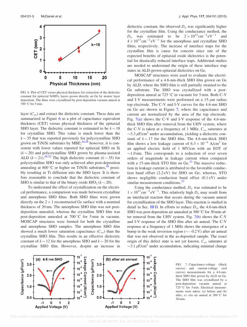
MOSCAP structures were used to evaluate the electri-
cal performance of a 4.6-nm-thick SHO film grown on Ge
by ALD, where the SHO film is still partially strained to the
Ge substrate. The SHO was crystallized with a post-
deposition anneal at 725 �C in vacuum for 5 min. Both C-V
and I-V measurements were performed on a 15-lm radius
top electrode. The C-V and I-V curves for the 4.6-nm SHO
on Ge are shown in Figure 7, where the capacitance and
current are normalized by the area of the top electrode.
Fig. 7(a) shows the C-V and I-V response of the 4.6-nm-
thick SHO film after removal from the UHV system, where
the C-V is taken at a frequency of 1 MHz. Cox saturates at
�3.3 lF/cm2 under accumulation, yielding a dielectric con-
stant of k� 17 for the SHO film. The 4.6-nm-thick SHO
film shows a low leakage current of 6.3� 10�6 A/cm2 for
an applied electric field of 1 MV/cm with an EOT of
�1.0 nm. This corresponds to a reduction of over seven
orders of magnitude in leakage current when compared
with a 15-nm-thick STO film on Ge.23 The massive reduc-
tion in leakage current is attributed to the favorable conduc-
tion band offset (2.2 eV) for SHO on Ge; whereas, STO
shows negligible conduction band offset (0.1 eV) under
similar measurement conditions.23
Using the conductance method, Dit was estimated to be
1� 1013 cm�2 eV�1. This relatively high Dit may result from
an interfacial reaction that occurs during the vacuum anneal
for crystallization of the SHO layer. This reaction is studied in
detail in Sec. III D. In efforts to reduce Dit, the 4.6-nm-thick
SHO was post-deposition air annealed at 300 �C for 30 min af-
ter removal from the UHV system. Fig. 7(b) shows the C-V
and I-V response of the SHO film after air anneal. The C-V
response at a frequency of 1 MHz shows the emergence of a
bump in the weak inversion region (��0.2 V) after air anneal
that was not observed in the as-deposited sample. The exact
origin of this defect state is not yet known. Cox saturates at
�3.1 lF/cm2 under accumulation, indicating minimal change
FIG. 6. Plot of CET versus physical thickness for extraction of the dielectric
constant for epitaxial SrHfO3 layers grown directly on Ge by atomic layer
deposition. The films were crystallized by post-deposition vacuum anneal at
700 �C for 5 min.
FIG. 7. Capacitance-voltage (black
curves) and current-voltage (red
curves) measurements for a 4.6-nm-
thick SHO film grown by ALD on Ge.
The SHO film was crystallized by a
post-deposition vacuum anneal at
725 �C for 5 min. Electrical measure-
ments were taken: (a) before and (b)
after, ex situ air anneal at 300 �C for
30 min.
054101-5 McDaniel et al. J. Appl. Phys. 117, 054101 (2015)
[This article is copyrighted as indicated in the article. Reuse of AIP content is subject to the terms at: http://scitation.aip.org/termsconditions. Downloaded to ] IP:
129.116.140.202 On: Tue, 10 Feb 2015 16:46:16

in the dielectric constant (k� 16). The leakage current is
slightly improved to 4.0� 10�6 A/cm2 for an applied electric
field of 1 MV/cm with an EOT of �1.1 nm. The Dit for the air
annealed sample was reduced to 6� 1012 cm�2 eV�1.
For comparison, the electrical performance of 2-nm-thick
crystalline SHO with a 2-nm-thick Al2O3 capping layer was
evaluated. The 2-nm-thick SHO film was crystallized at a rel-
atively lower temperature of 650 �C, leading to a more abrupt
interface, as discussed in Sec. III D. The Al2O3 capping layer
was needed to prevent excess leakage current through the thin
SHO layer. With this dielectric stack, the crystalline SHO
layer is used to minimize Dit at the oxide-Ge interface and the
amorphous Al2O3 is an excellent leakage barrier. Figure 8
shows the C-V and I-V response of the SHO/Al2O3 dielectric
stack on Ge after air annealing at 300 �C for 30 min. The
SHO/Al2O3 stack has a very low leakage current of
1.9� 10�7 A/cm2 for an applied electric field of 1 MV/cm
with an EOT of �1.5 nm. As expected, the overall Cox satu-
rates at a lower value (�2.3 lF/cm2) than the 4.6-nm-thick
SHO film. Once again, a small bump is observed in the weak
inversion region of the C-V response after air anneal.
Assuming a dielectric constant of k� 18 for the SHO film, the
dielectric constant of the Al2O3 capping layer is k� 8. This
value is consistent with other reports of Al2O3 deposited by
ALD with the same co-reactants under similar conditions.54,55
The Dit for the SHO/Al2O3 dielectric stack is estimated to be
2� 1012 cm�2 eV�1. We attribute this lower Dit value to the
lower annealing temperature (650 �C) required to crystallize
the SHO film. More detailed analysis of the electrical per-
formance and origin of defect states in crystalline SHO on Ge
will be the subject of future work.
D. Crystallization temperature and the SrHfO3-Geinterface
In all cases, strontium hafnate films deposited by ALD
required post-deposition annealing for crystallization; how-
ever, the onset of crystallization varied between 650 and
750 �C depending on the thickness of the SHO film. The
lowest crystallization temperature observed was at a sub-
strate temperature of 650 �C for a 2-nm-thick SHO film. For
very thin (�1 nm) SHO films, the temperature required for
crystallization increased to 750 �C due to the substrate
retarding crystallization. In all cases, SHO films between 2
and 20-nm-thick appeared fully crystallized when vacuum
annealed at a substrate temperature of 700 �C for 5 min. At
700 �C, the temperature is approximately 80% of the Ge
melting point (�940 �C), which could lead to interfacial
instabilities due to Ge diffusion. In the previous work, inter-
facial reaction between Ge and Hf metal has been reported
to cause formation of a hafnium germanide (HfGe2) at tem-
peratures above �600 �C.56
The effects of annealing temperature on the SHO-Ge
heterostructure were examined by in situ RHEED and XPS.
A very thin (�1 nm) SHO film was used so that the subtle
changes in the Ge 3 d core-level with increasing anneal tem-
perature could be observed. A series of RHEED patterns are
shown in Figures 9(a)–9(c). The crystallization of the film
can be observed at increasing temperatures of 650, 750, and
850 �C. At the lowest temperature of 650 �C (Fig. 9(a)), the
SHO film appears amorphous. The film is thin enough that
some electron diffraction is observed from the underlying Ge
substrate. After annealing to 750 �C (Fig. 9(b)), the SHO
film appears crystalline as shown by the appearance of an or-
dered streak pattern. The beam is aligned along the h100idirection of the film. When annealed at 850 �C (Fig. 9(c)),
the diffraction patterns are more prominent. However, there
are additional 1/2-order streaks present that may be due to a
secondary phase formation at the interface.
The corresponding series of Ge 3d spectra collected by insitu XPS shown in Figs. 9(d)–9(f) provide insight into the
interfacial reaction that occurs between SHO and Ge. The
overall Ge 3d signal becomes less defined (broader) with
increasing anneal temperature. Deconvolution of the Ge 3dcore-level in CasaXPS also reveals that spectral components
of both lower and higher binding energy than the bulk peak
increase with higher temperature annealing. The lower bind-
ing energy component is attributed to a combination of
“interfacial Ge” and Ge-Hf bonding. The chemical shift
(De¼�0.5 eV) observed for the interfacial Ge component
appears similar to Ge (001) surface dimerization.57 A similar
chemical shift (�0.46 eV) is expected for Ge-Hf bonding
from first-principles calculations.58 The percentage of the Ge
3d5/2 component associated with the lower binding energy rel-
ative to the entire Ge signal is shown to increase with temper-
ature. The relative area of this component is 2.2%, 2.7%, and
5.6% for the film annealed at 650 �C, 750 �C, and 850 �C,
respectively. We associate the increase in this component
with an interfacial reaction between SHO and Ge with
increasing temperature, although the small difference in rela-
tive area between 650 �C and 750 �C may not be significant.
The more substantial change in the relative area of the lower
binding energy component at 850 �C is attributed to an
increase in Ge-Hf bonding. There is also an increase in the
higher binding energy component, which is attributed to Ge1þ
formation (De¼ 0.70 eV).59 At higher annealing temepera-
tures, desorption of the SHO film may occur; however, no
noticeable changes in the Sr 3d or O 1s core-levels were
observed after annealing at 850 �C (not shown). Only a slight
shift (�0.2 eV) to lower binding energy was observed in the
FIG. 8. Capacitance-voltage (black curve) and current-voltage (red curve)
measurements for 2-nm-thick SHO film on Ge with a 2-nm-thick Al2O3 cap-
ping layer. The SHO film was crystallized by a post-deposition vacuum
anneal at 650 �C for 5 min before depositing the amorphous Al2O3 capping
layer.
054101-6 McDaniel et al. J. Appl. Phys. 117, 054101 (2015)
[This article is copyrighted as indicated in the article. Reuse of AIP content is subject to the terms at: http://scitation.aip.org/termsconditions. Downloaded to ] IP:
129.116.140.202 On: Tue, 10 Feb 2015 16:46:16

Hf 4f core-level with increased annealing temperature (not
shown), which is also attributed to an increase in Ge-Hf
bonding.
As further confirmation of an interfacial reaction, the
SHO-Ge heterostructure was explored by cross-sectional
TEM observations. SHO films were vacuum annealed at
650 �C and 700 �C to compare the abruptness of the SHO-Ge
interface. The 2-nm-thick SHO film was post-deposition
annealed at 650 �C for 5 min and then capped with 2 nm of
amorphous Al2O3 before removal from the UHV system.
The thicker SHO film (5.2-nm-thick) was annealed at 700 �Cand was removed from the system without a capping layer.
The 5.2-nm-thick SHO film was grown in a two-step growth
and anneal process (2 nm plus 3.2 nm) with post-deposition
annealing at 700 �C for 5 min following each growth.
Electron micrographs of the two films are compared in
Figure 10. At a substrate temperature of 650 �C (Fig. 10(a)),
the SHO-Ge interface appears abrupt with a negligible inter-
facial layer (IL). However, for the higher substrate tempera-
ture of 700 �C (Fig. 10(b)), there is a clear presence of an IL
at the SHO-Ge interface. The thickness of this IL appears to
be �0.5 nm, indicating that the interfacial reaction here is
limited to 1–2 atomic layers. Regardless, this IL formation
appears correlated to higher Dit values as discussed Sec.
III C. The electron micrographs, along with the XPS analy-
sis, indicate that a low crystallization temperature (<650 �C)
is necessary to maintain an abrupt interface for the SHO-Ge
heterojunction. An abrupt interface may be necessary to
reduce Dit for the desired electrical performance of the crys-
talline oxide on Ge.
With this material system, there is a tradeoff between
sufficient thermal energy for crystallization to achieve a
higher dielectric constant, while also maintaining a lower
temperature to minimize interfacial reactions and Dit. As
mentioned above, the 2-nm-thick SHO film began crystalliz-
ing at the lowest temperature of 650 �C. However, typical
SHO films grown by this method crystallized somewhere
between 650–700 �C, appearing fully crystalline by RHEED
at 700 �C. The obvious concern is that at temperatures below
700 �C, films will not be fully crystallized and suffer from a
lower dielectric constant. As a complicating factor, higher
anneal temperatures are also correlated with increasing Dit
values. The lowest Dit values for SHO on Ge were measured
for films with no post-deposition anneal (amorphous films)
or where the post-deposition anneal was kept at or below
650 �C. Low magnification electron micrographs of the two
films discussed above are shown in Figure 11. The top image
(Fig. 11(a)) reveals that the SHO film annealed at 650 �C has
some tiny isolated amorphous regions, as denoted by the
FIG. 9. Effects of annealing temperature on the SHO-Ge heterostructure examined by in situ RHEED and XPS. RHEED patterns are shown at increasing
anneal temperatures of (a) 650 �C, (b) 750 �C, and (c) 850 �C. The corresponding Ge 3d core-level spectra are shown in (d)–(f) for the 650–850 �C anneal tem-
perature, respectively. The extent of interfacial reaction is quantified by the percent of Ge 3d5/2 for the lower binding energy component relative to the total Ge
signal, as shown graphically on the right side of the high-resolution scan.
FIG. 10. Transmission electron micrographs of: (a) 2-nm-thick SHO post-
deposition annealed at 650 �C for 5 min and then capped with 2 nm of amor-
phous Al2O3 and (b) 5.2-nm-thick SHO film grown in a two-step growth and
anneal process (2 nm and 3.2 nm) with post-deposition annealing at 700 �Cfor 5 min. A higher anneal temperature of 700 �C, results in the formation of
a very thin IL at the SHO-Ge interface.
054101-7 McDaniel et al. J. Appl. Phys. 117, 054101 (2015)
[This article is copyrighted as indicated in the article. Reuse of AIP content is subject to the terms at: http://scitation.aip.org/termsconditions. Downloaded to ] IP:
129.116.140.202 On: Tue, 10 Feb 2015 16:46:16

arrows. The thicker SHO film annealed at 700 �C, shown in
Fig. 11(b), does not show any sign of amorphous regions. In
both cases, the SHO films show excellent epitaxial alignment
with the Ge substrate, and the deposited films are uniform in
thickness. Further study is clearly required to optimize the
annealing conditions to achieve high crystallinity to increase
the dielectric constant, while maintaining an abrupt interface
to minimize interface traps.
IV. CONCLUSIONS
Crystalline strontium hafnate, SrHfO3 (SHO), films
have been grown by atomic layer deposition directly on Ge
(001) substrates. The 2� 1 reconstructed Ge (001) surface
was prepared by thermal annealing in vacuum and trans-
ferred in situ to the ALD system. After deposition of an
amorphous SHO layer (�2–20 nm), the film was crystallized
by post-deposition anneal (�700 �C) in vacuum. The crystal-
line SHO films were confirmed to be (001)-oriented with epi-
taxial registry to the Ge (001) surface. Band offset
measurements indicate that the SHO has favorable band off-
sets with Ge for gate dielectric applications, with a VBO of
�3.27 eV and CBO of 2.17 eV. Electrical measurements of
MOSCAP structures estimate the dielectric constant of crys-
talline SHO to be k� 18. The leakage current of a 4.6-nm-
thick SHO film was 6.3� 10�6 A/cm2 for an applied electric
field of 1 MV/cm, which indicates a significant advantage of
Hf-based perovskites over Ti-based perovskites, such as
STO. The lowest Dit value for the SHO-Ge heterojunction
was estimated to be 2� 1012 cm�2 eV�1. Interestingly, Dit is
not improved by crystallization of the SHO layer and is neg-
atively impacted by higher post-deposition annealing tem-
perature and corresponding abruptness of the SHO-Ge
interface. The current work shows extremely promising
potential for the integration of crystalline oxides on Ge by
atomic layer deposition for advanced electronic applications.
ACKNOWLEDGMENTS
This work was supported by the National Science
Foundation (Award Nos. CMMI-1437050 and DMR-
1207342), the Office of Naval Research (Grant No. N00014-
10-10489), and the Air Force Office of Scientific Research
(Grant No. FA9550-12-10494).
1K. Rim, R. Anderson, D. Boyd, F. Cardone, K. Chan, H. Chen, S.
Christansen, J. Chu, K. Jenkins, T. Kanarsky, S. Koester, B. H. Lee, K.
Lee, V. Mazzeo, A. Mocuta, D. Mocuta, P. M. Mooney, P. Oldiges, J. Ott,
P. Ronsheim, R. Roy, A. Steegen, M. Yang, H. Zhu, M. Ieong, and H. S.
P. Wong, Solid-State Electron. 47, 1133 (2003).2S. E. Thompson, M. Armstrong, C. Auth, M. Alavi, M. Buehler, R. Chau,
S. Cea, T. Ghani, G. Glass, and T. Hoffman, IEEE Trans. Electron.
Devices 51, 1790 (2004).3R. Chau, B. Doyle, S. Datta, J. Kavalieros, and K. Zhang, Nat. Mater. 6,
810 (2007).4K. C. Saraswat, C. O. Chui, T. Krishnamohan, A. Nayfeh, and P.
McIntyre, Microelectron. Eng. 80, 15 (2005).5D. P. Brunco, B. De Jaeger, G. Eneman, A. Satta, V. Terzieva, L. Souriau,
F. E. Leys, G. Pourtois, M. Houssa, K. Opsomer, G. Nicholas, M.
Meurius, and M. Heyns, ECS Trans. 11, 479 (2007).6R. Pillarisetty, Nature 479, 324 (2011).7S. Gupta, X. Gong, R. Zhang, Y.-C. Yeo, S. Takagi, and K. C. Saraswat,
MRS Bull. 39, 678 (2014).8R. Droopad, K. Eisenbeiser, and A. A. Demkov, in High DielectricConstant Materials, edited by H. R. Huff and D. C. Gilmer (Springer,
Berlin, Heidelberg, 2005), Vol. 16, p. 639.9R. A. McKee, F. J. Walker, and M. F. Chisholm, Phys. Rev. Lett. 81, 3014
(1998).10R. Droopad, Z. Yu, J. Ramdani, L. Hilt, J. Curless, C. Overgaard, J. L.
Edwards, Jr., J. Finder, K. Eisenbeiser, and W. Ooms, Mater. Sci. Eng. B
87, 292 (2001).11R. John, Rep. Prog. Phys. 69, 327 (2006).12A. A. Demkov, A. B. Posadas, H. Seo, M. Choi, K. J. Kormondy, P.
Ponath, R. C. Hatch, M. D. McDaniel, T. Q. Ngo, and J. G. Ekerdt, ECS
Trans. 54, 255 (2013).13C. Claeys and E. Simoen, Germanium-Based Technologies: From Materials
to Devices (Elsevier Science, 2007).14Y. Kamata, Mater. Today 11, 30 (2008).15K. Kita, T. Takahashi, H. Nomura, S. Suzuki, T. Nishimura, and A.
Toriumi, Appl. Surf. Sci. 254, 6100 (2008).16M. Caymax, M. Houssa, G. Pourtois, F. Bellenger, K. Martens, A.
Delabie, and S. Van Elshocht, Appl. Surf. Sci. 254, 6094 (2008).17R. M. Wallace, P. C. McIntyre, J. Kim, and Y. Nishi, MRS Bull. 34, 493
(2009).18I.-K. Oh, M.-K. Kim, J.-S. Lee, C.-W. Lee, C. Lansalot-Matras, W. Noh,
J. Park, A. Noori, D. Thompson, S. Chu, W. J. Maeng, and H. Kim, Appl.
Surf. Sci. 287, 349 (2013).19K. D. Fredrickson, P. Ponath, A. B. Posadas, M. R. McCartney, T. Aoki,
D. J. Smith, and A. A. Demkov, Appl. Phys. Lett. 104, 242908 (2014).20R. A. McKee, F. J. Walker, and M. F. Chisholm, Science 293, 468 (2001).21S. A. Chambers, Y. Liang, Z. Yu, R. Droopad, and J. Ramdani, J. Vac.
Sci. Technol. A 19, 934 (2001).22F. Amy, A. S. Wan, A. Kahn, F. J. Walker, and R. A. McKee, J. Appl.
Phys. 96, 1635 (2004).23M. D. McDaniel, T. Q. Ngo, A. Posadas, C. Hu, S. Lu, D. J. Smith, E. T.
Yu, A. A. Demkov, and J. G. Ekerdt, Adv. Mater. Interfaces 1(8), 1400081
(2014).24I. McCarthy, M. P. Agustin, S. Shamuilia, S. Stemmer, V. V. Afanas’ev,
and S. A. Campbell, Thin Solid Films 515, 2527 (2006).25C. Rossel, B. Mereu, C. Marchiori, D. Caimi, M. Sousa, A. Guiller, H.
Siegwart, R. Germann, J. P. Locquet, J. Fompeyrine, D. J. Webb, C.
Dieker, and J. W. Seo, Appl. Phys. Lett. 89, 053506 (2006).26M. Sousa, C. Rossel, C. Marchiori, H. Siegwart, D. Caimi, J.-P. Locquet,
D. J. Webb, R. Germann, J. Fompeyrine, K. Babich, J. W. Seo, and C.
Dieker, J. Appl. Phys. 102, 104103 (2007).27C. Rossel, M. Sousa, C. Marchiori, J. Fompeyrine, D. Webb, D. Caimi, B.
Mereu, A. Ispas, J. P. Locquet, H. Siegwart, R. Germann, A. Tapponnier,
and K. Babich, Microelectron. Eng. 84, 1869 (2007).28G. Lupina, G. Kozłowski, J. Dabrowski, P. Dudek, G. Lippert, and H.-J.
MussigMussig, Appl. Phys. Lett. 93, 252907 (2008).29G. Łupina, O. Seifarth, G. Kozłowski, P. Dudek, J. Dabrowski, G. Lippert,
and H. J. M€ussig, Microelectron. Eng. 86, 1842 (2009).30M. Sawkar-Mathur, C. Marchiori, J. Fompeyrine, M. F. Toney, J. Bargar,
and J. P. Chang, Thin Solid Films 518, S118 (2010).
FIG. 11. Low magnification electron micrographs of: (a) 2-nm-thick SHO
film post-deposition annealed at 650 �C for 5 min and then capped with 2 nm
of amorphous Al2O3 and (b) 5.2-nm-thick SHO film grown in a two-step
growth and anneal process (2 nm and 3.2 nm) with post-deposition annealing
at 700 �C for 5 min. Tiny amorphous regions are visible in (a), attributed to
the reduced post-deposition anneal temperature.
054101-8 McDaniel et al. J. Appl. Phys. 117, 054101 (2015)
[This article is copyrighted as indicated in the article. Reuse of AIP content is subject to the terms at: http://scitation.aip.org/termsconditions. Downloaded to ] IP:
129.116.140.202 On: Tue, 10 Feb 2015 16:46:16

31G. Lupina, O. Seifarth, P. Dudek, G. Kozlowski, J. Dabrowski, H.-J.
Thieme, G. Lippert, T. Schroeder, and H.-J. M€ussig, Phys. Status Solidi B
248, 323 (2011).32K. Black, M. Werner, R. Rowlands–Jones, P. R. Chalker, and M. J.
Rosseinsky, Chem. Mater. 23, 2518 (2011).33A. S. Verma and V. K. Jindal, J. Alloys Compd. 485, 514 (2009).34L. Bjaalie, B. Himmetoglu, L. Weston, A. Janotti, and C. G. Van de
Walle, New J. Phys. 16, 025005 (2014).35X. Zhang, A. A. Demkov, H. Li, X. Hu, Y. Wei, and J. Kulik, Phys. Rev.
B 68, 125323 (2003).36Manufactured and supplied by Air Liquide ALOHA Electronics
Performance Materials, Air Liquide Electronics U.S. LP, Houston,
TX.37Manufactured and supplied by Dow Electronic Materials, The Dow
Chemical Company, North Andover, MA.38M. Vehkam€aki, T. Hatanp€a€a, T. H€anninen, M. Ritala, and M. Leskel€a,
Electrochem. Solid-State Lett. 2, 504 (1999).39M. Vehkam€aki, T. H€anninen, M. Ritala, M. Leskel€a, T. Sajavaara, E.
Rauhala, and J. Keinonen, Chem. Vap. Deposition 7, 75 (2001).40R. Katamreddy, V. Omarjee, B. Feist, C. Dussarrat, M. Singh, and C.
Takoudis, ECS Trans. 16, 487 (2008).41R. Katamreddy, Z. Wang, V. Omarjee, P. V. Rao, C. Dussarrat, and N.
Blasco, ECS Trans. 25, 217 (2009).42B. Willis and C. B. Zhang, ECS Trans. 33, 51 (2010).43C. B. Zhang, L. Wielunski, and B. G. Willis, Appl. Surf. Sci. 257, 4826
(2011).44S. W. Lee, J. H. Han, S. Han, W. Lee, J. H. Jang, M. Seo, S. K. Kim, C.
Dussarrat, J. Gatineau, Y.-S. Min, and C. S. Hwang, Chem. Mater. 23,
2227 (2011).
45W. Lee, J. H. Han, W. Jeon, Y. W. Yoo, S. W. Lee, S. K. Kim, C.-H. Ko,
C. Lansalot-Matras, and C. S. Hwang, Chem. Mater. 25, 953 (2013).46M. D. McDaniel, A. Posadas, T. Q. Ngo, A. Dhamdhere, D. J. Smith, A. A.
Demkov, and J. G. Ekerdt, J. Vac. Sci. Technol. A 31, 01A136 (2013).47M. D. McDaniel, A. Posadas, T. Q. Ngo, C. M. Karako, J. Bruley, M. M.
Frank, V. Narayanan, A. A. Demkov, and J. G. Ekerdt, J. Appl. Phys. 115,
224108 (2014).48H. Li and D. V. Shenai, Symposium C - CMOS Gate-Stack Scaling-Materials,
Interfaces and Reliability Implications (Mater. Res. Soc. Symp. Proc., 2009),
Vol. 1155, p. C04.49C. D. Wagner, J. Electron. Spectrosc. Relat. Phenom. 32, 99 (1983).50K. Martens, C. O. Chui, G. Brammertz, B. De Jaeger, D. Kuzum, M.
Meuris, M. M. Heyns, T. Krishnamohan, K. Saraswat, H. E. Maes, and G.
Groeseneken, IEEE Trans. Electron. Devices 55, 547 (2008).51S. Yamanaka, T. Maekawa, H. Muta, T. Matsuda, S.-i. Kobayashi, and K.
Kurosaki, J. Alloys Compd. 381, 295 (2004).52O. Madelung, Semiconductors-Data Handbook (Springer, 2004).53D. G. Schlom, S. Guha, and S. Datta, MRS Bull. 33, 1017 (2008).54M. D. Groner, J. W. Elam, F. H. Fabreguette, and S. M. George, Thin
Solid Films 413, 186 (2002).55M. D. Groner, F. H. Fabreguette, J. W. Elam, and S. M. George, Chem.
Mater. 16, 639 (2004).56S. Gaudet, C. Detavernier, A. J. Kellock, P. Desjardins, and C. Lavoie,
J. Vac. Sci. Technol. A 24, 474 (2006).57P. E. J. Eriksson and R. I. G. Uhrberg, Phys. Rev. B 81, 125443 (2010).58G. Pourtois, M. Houssa, A. Delabie, T. Conard, M. Caymax, M. Meuris,
and M. M. Heyns, Appl. Phys. Lett. 92, 032105 (2008).59A. Molle, M. N. K. Bhuiyan, G. Tallarida, and M. Fanciulli, Appl. Phys.
Lett. 89, 083504 (2006).
054101-9 McDaniel et al. J. Appl. Phys. 117, 054101 (2015)
[This article is copyrighted as indicated in the article. Reuse of AIP content is subject to the terms at: http://scitation.aip.org/termsconditions. Downloaded to ] IP:
129.116.140.202 On: Tue, 10 Feb 2015 16:46:16