atomic layer deposition of (k,na)(nb,ta)o3 thin films ... · atomic layer deposition of...
TRANSCRIPT
Atomic layer deposition of (K,Na)(Nb,Ta)O3 thin films
Henrik Hovde Sønsteby, Ola Nilsen, and Helmer Fjellvåg
Citation: Journal of Vacuum Science & Technology A: Vacuum, Surfaces, and Films 34, 041508 (2016); doi:10.1116/1.4953406View online: http://dx.doi.org/10.1116/1.4953406View Table of Contents: http://avs.scitation.org/toc/jva/34/4Published by the American Vacuum Society
Articles you may be interested inCrystallinity of inorganic films grown by atomic layer deposition: Overview and general trendsJournal of Vacuum Science & Technology A: Vacuum, Surfaces, and Films 113, 021301021301 (2013);10.1063/1.4757907
Atomic layer deposition of (K,Na)(Nb,Ta)O3 thin films
Henrik Hovde Sønsteby,a) Ola Nilsen, and Helmer FjellvagDepartment of Chemistry, University of Oslo, Sem Sælands vei 26, 0371 Oslo, Norway
(Received 1 March 2016; accepted 23 May 2016; published 8 June 2016)
Thin films of complex alkali oxides are frequently investigated due to the large range of electric
effects that are found in this class of materials. Their piezo- and ferroelectric properties also place
them as sustainable lead free alternatives in optoelectronic devices. Fully gas-based routes for dep-
osition of such compounds are required for integration into microelectronic devices that need con-
formal thin films with high control of thickness- and composition. The authors here present a route
for deposition of materials in the (K,Na)(Nb,Ta)O3-system, including the four end members
NaNbO3, KNbO3, NaTaO3, and KTaO3, using atomic layer deposition with emphasis on control of
stoichiometry in such mixed quaternary and quinary compunds. VC 2016 American Vacuum Society.
[http://dx.doi.org/10.1116/1.4953406]
I. INTRODUCTION
Thin films of AIBVO3 perovskites based on alkaline AI
elements obtain an increasing amount of attention due to the
many important physical properties that are found in materi-
als of this class. LiNbO3 and KxNa1�xNbO3 are both consid-
ered strong candidates as sustainable lead free piezo- and
ferroelectrics in many applications.1–5 LiTaO3 is renowned
for its piezoelectric properties.6 Anion doped NaTaO3 is
used in visible light photocatalysis.7 KNbO3 is already in use
in devices utilizing surface acoustic waves and in nonlinear
optics.8,9 KTaO3 is under investigation for forming a 2D
electron gas at interfaces toward LaTiO3 analogous to the
SrTiO3kLaAlO3 heteroepitaxial system.10 In addition to this,
multilayer stacks of KTaO3kKNbO3 are reported to exhibit a
strong ferroelectric response.11
Thin films of several AIBVO3-materials have been de-
posited using physical deposition techniques such as pulsed
laser deposition, molecular beam epitaxy and sputter-
ing;12–21 however, reports on low temperature chemical
deposition routes are very limited. Thin films of LiNbO3,
LiTaO3, and KNbO3 have been grown using chemical
vapor deposition,22–24 and LiNbO3 and LiTaO3 is also
reported by atomic layer deposition (ALD).25,26 ALD
would indeed be the technique of choice in many the poten-
tial applications due to excellent thickness control and con-
formality of the deposited films, in particular, on very high
aspect ratio substrates.27 These are crucial features in appli-
cations utilizing surface acoustic waves and in optoelec-
tronics. However, the lack of suitable precursors has so far
limited the possibility of ALD-grown sodium- and potas-
sium containing thin films. In 2014, ALD of sodium- and
potassium aluminates were reported for the first time,
thereby opening for growth of a range of materials contain-
ing these elements.28
In this work, ALD of the four-component (K,Na)(Nb,Ta)O3-
system is investigated. In addition to this, evidence of complete
intermixing of all the four end members is provided.
II. EXPERIMENT
All thin films in this work were deposited using a Beneq
TFS-500 atomic layer deposition reactor. The depositions were
carried out at 3 mbar working pressure, with N2 as the carrier-
and purging gas. Nitrogen gas was supplied from a Schmidelin-
Sirrco 5 generator providing >99.9995% (N2þAr) before
purification through a Mykrolis purifier. Reactor temperature
was maintained at 250 �C unless otherwise stated, consistent
with previous reports of ALD-growth of similar compounds.
Sodium- and potassium tert-butoxide were used as alkali
metal sources, supplied from HS-300 sources at 140 and
150 �C, respectively. Niobium- and tantalum ethoxide was
used as group V metal sources, supplied from a HS-500
source at 68 and 70 �C, respectively. The precursors were
supplied through heated valves. The metalorganic precursors
used are summarized in Table I. Distilled water was used as
the oxygen source. The water pulse was set to 0.25 s, and the
purge duration to 1 s for all experiments. The tert-butoxides
were pulsed for 3 s whereas the ethoxides were pulsed for
2 s. All pulse and purge parameters are well within self-
limiting growth as shown by earlier experiments.28–30
All systems were developed by depositing on Si(100)
1� 1 cm2 single crystal substrates. A Pt-coated Si(100) sub-
strate was used for piezoelectric characterization of one
K0.5Na0.5NbO3 thin film.
Thin film thickness was measured using a J. A. Woolam
a-SE spectroscopic ellipsometer in the range of 390–900 nm.
A Cauchy-function was used to model the data assuming the
films were transparent in this wavelength range.
Cation compositions of the films were measured with
standardless x-ray fluorescence spectroscopy using a Philips
TABLE I. Overview of the precursors used.
Chemical name Formula Supplier Purity
Sodium tert-butoxide NaOC(CH3)3 Aldrich 97%
Potassium tert-butoxide KOC(CH3)3 Aldrich 98%
Niobium ethoxide Nb(OCH2CH3)5 Aldrich 99.9%
Tantalum ethoxide Ta(OCH2CH3)5 Aldrich 99.9%a)Electronic mail: [email protected]
041508-1 J. Vac. Sci. Technol. A 34(4), Jul/Aug 2016 0734-2101/2016/34(4)/041508/6/$30.00 VC 2016 American Vacuum Society 041508-1
PW2400 XRF and analyzed using the UNIQUANT software
package.
Complementary measurements of composition using x-ray
photoelectron spectroscopy were performed using a Thermo
Scientific Theta Probe Angle-Resolved XPS system, also en-
abling measurements of carbon contaminants and possible
segregation of the cations in the films. The instrument is
equipped with a standard Al Ka source (h�¼ 1486.6 eV), and
the analysis chamber pressure is in the order of 10�8 mbar.
Pass energy values of 200 and 50 eV were used for survey
spectra and detailed scans, respectively.
Crystallographic studies were performed on a PANalytical
Empyrean diffractometer equipped with a Cu Ka (k¼1.5406 A) source powered at 45 kV and 40 mA. A parallel
beam x-ray mirror and a proportional point detector were used
for grazing incidence x-ray diffraction (GIXRD) measurements.
Morphology studies were performed using a Park Systems
XE-70 AFM equipped with a standard non-contact high-
resolution tip. Data were analyzed using the Gwyddion 2.43
SPM visualization tool.31 The same apparatus equipped with
an enhanced piezoresponse force microscopy (PFM) tip and
lock-in amplifier was used for mapping of piezoelectric
domains in a K0.5Na0.5NbO3 thin film.32 PFM works by
applying an AC current through a conductive AFM tip to
achieve piezoelectric deformation of the sample, thereby
directly measuring the piezoelectric domains.
III. RESULTS AND DICSUSSION
A. Thin film growth
The thin films were in general grown as a mix of two,
three, or four well known processes for binary systems: K-O,
Na-O, Nb-O, and Ta-O. In all these processes, water is used
as the oxygen source, keeping the amount of precursors to a
minimum and ruling out issues with stronger oxidizing agents
such as O3 that may interfere with layer-by-layer growth of
the alkali metal precursors. This effect was seen for the alkali
aluminate systems, where the ozone based process resulted in
higher carbon contamination due to formation of carbo-
nates.28 Tantalum oxide and niobium oxide were deposited
with a growth rate of 0.40 6 0.01 and 0.38 6 0.01 A/cycle,
respectively, close to previously reported values by Kukli
et al.29,30 It is not possible to examine the alkali metal binary
systems as pure oxides due to the formation of hydroxides or
carbonates. They were therefore initially deposited as alumi-
nates as described by Østreng et al. to verify similar growth
rates.28 All precursors exhibit self-limiting reactions with tra-
ditional ALD type growth for the pulse parameters applied
(also see the supplementary material).33
The four end AIBVO3-members in the (K,Na)(Nb,Ta)O3-
system were deposited by combining two binary systems to
create a ternary reaction cycle. The net super cycle for all
four compounds can be described as
n½ðK=NaÞOCðCH3Þ3 þ H2O�þ m½ðNb=TaÞðOCH2CH3Þ5 þ H2O�:
The pulsing sequence was chosen as to facilitate maxi-
mum mixing, i.e., a pulsed net 2:3 ratio was deposited as
(K/Na)þ (Nb/Ta)þ (K/Na)þ (Nb/Ta)þ (Nb/Ta). All four
end member systems showed typical ALD-behavior, and con-
formal thin films were obtained. The required n and m values
for obtaining stoichiometric ABO3-phases vary slightly
between the systems, but are generally very close to
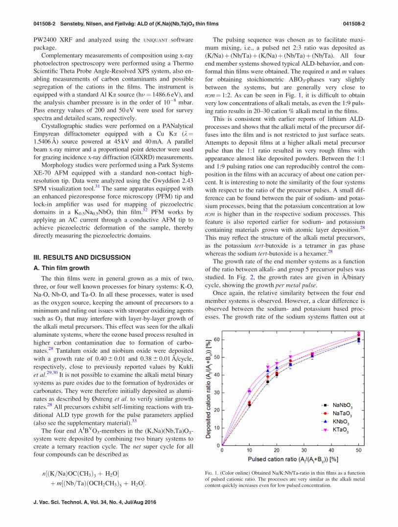
n:m¼ 1:2. As can be seen in Fig. 1, it is difficult to obtain
very low concentrations of alkali metals, as even the 1:9 puls-
ing ratio results in 20–30 cation % alkali metal in the films.
This is consistent with earlier reports of lithium ALD-
processes and shows that the alkali metal of the precursor dif-
fuses into the film and is not restricted to just surface seats.
Attempts to deposit films at a higher alkali metal precursor
pulse than the 1:1 ratio resulted in very rough films with
appearance almost like deposited powders. Between the 1:1
and 1:9 pulsing ratios one can reproducibly control the com-
position in the films with an accuracy of about one cation per-
cent. It is interesting to note the similarity of the four systems
with respect to the ratio of the precursor pulses. A small dif-
ference can be found between the pair of sodium- and potas-
sium processes, being that the potassium concentration at low
n:m is higher than in the respective sodium processes. This
feature is also reported earlier for sodium- and potassium
containing materials grown with atomic layer deposition.28
This may reflect the structure of the alkali metal precursors,
as the potassium tert-butoxide is a tetramer in gas phase
whereas the sodium tert-butoxide is a hexamer.28
The growth rate of the end member systems as a function
of the ratio between alkali- and group 5 precursor pulses was
studied. In Fig. 2, the growth rates are given in A/binary
cycle, showing the growth per metal pulse.
Once again, the relative similarity between the four end
member systems is observed. However, a clear difference is
observed between the sodium- and potassium based proc-
esses. The growth rate of the sodium systems flatten out at
FIG. 1. (Color online) Obtained Na/K:Nb/Ta-ratio in thin films as a function
of pulsed cationic ratio. The processes are very similar as the alkali metal
content quickly increases even for low pulsed concentration.
041508-2 Sønsteby, Nilsen, and Fjellvag: ALD of (K,Na)(Nb,Ta)O3 thin films 041508-2
J. Vac. Sci. Technol. A, Vol. 34, No. 4, Jul/Aug 2016
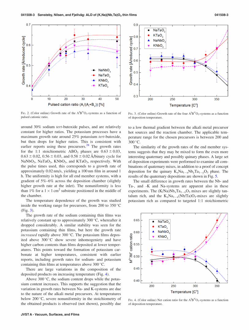
around 30% sodium tert-butoxide pulses, and are relatively
constant for higher ratios. The potassium processes have a
maximum growth rate around 25% potassium tert-butoxide,
but then drops for higher ratios. This is consistent with
earlier reports using these precursors.28 The growth rates
for the 1:1 stoichiometric ABO3 phases are 0.63 6 0.03,
0.63 6 0.02, 0.56 6 0.03, and 0.58 6 0.02 A/binary cycle for
NaNbO3, NaTaO3, KNbO3, and KTaO3, respectively. With
the pulse times used, this corresponds to a growth rate of
approximately 0.02 nm/s, yielding a 100 nm film in around 1
h. The uniformity is high for all end member systems, with a
gradient of 5%–6% across the deposition chamber (slightly
higher growth rate at the inlet). The nonuniformity is less
than 1% for a 1� 1 cm2 substrate positioned in the middle of
the chamber.
The temperature dependence of the growth was studied
inside the working range for precursors, from 200 to 350 �C(Fig. 3).
The growth rate of the sodium containing thin films was
relatively constant up to approximately 300 �C, whereafter it
dropped considerably. A similar stability was seen for the
potassium containing thin films, but here the growth rate
increased rapidly above 300 �C. The potassium films depos-
ited above 300 �C show severe inhomogeniety and have
higher carbon contents than films deposited at lower temper-
atures. This points toward the formation of potassium car-
bonate at higher temperatures, consistent with earlier
reports, including growth rates for sodium- and potassium
containing thin films at temperatures above 300 �C.
There are large variations in the composition of the
deposited products on increasing temperature (Fig. 4).
Above 300 �C, the sodium content drops while the potas-
sium content increases. This supports the suggestion that the
variation in growth rates between Na- and K-systems are due
to the nature of the alkali metal precursors. At temperatures
below 200 �C, severe nonuniformity in the stoichiometry of
the obtained products is observed (not shown), possibly due
to a low thermal gradient between the alkali metal precursor
hot sources and the reaction chamber. The applicable tem-
perature range for the chosen precursors is between 200 and
300 �C.
The similarity of the growth rates of the end member sys-
tems suggests that they may be mixed to form the even more
interesting quaternary and possibly quinary phases. A large set
of deposition experiments were performed to examine all com-
binations of quaternary mixes, in addition to a proof of concept
deposition for the quinary KxNa1�xNbyTa1�yO3 phase. The
results of the quaternary depositions are shown in Fig. 5.
The small difference in growth rates between the Nb- and
Ta-, and -K and Na-systems are apparent also in these
experiments. The (K/Na)NbxTa1�xO3 mixes are slightly tan-
talum rich, and the KxNa1�x(Nb/Ta)O3-mixes are slightly
potassium rich as compared to targeted 1:1 stoichiometric
FIG. 2. (Color online) Growth rate of the AIBVO3-systems as a function of
pulsed cationic ratio.FIG. 3. (Color online) Growth rate of the four AIBVO3-systems as a function
of deposition temperature.
FIG. 4. (Color online) Net cation ratio for the AIBVO3-systems as a function
of deposition temperature.
041508-3 Sønsteby, Nilsen, and Fjellvag: ALD of (K,Na)(Nb,Ta)O3 thin films 041508-3
JVST A - Vacuum, Surfaces, and Films

mixing. However, tuning of pulsed ratios is well feasible in
order to obtain targeted phases and compositions. For proof
of concept, a stoichiometric K0.5Na0.5NbO3 thin film was de-
posited using a pulsed K:Na ratio of 48:52.
The quinary KxNa1�xNbyTa1�yO3-phase was deposited to
fully prove the complete mixing of the involved cation sys-
tems, yielding a close to stoichiometric K0.5Na0.5Nb0.5Ta0.5O3
film at K:Na¼ 48:52 and Nb:Ta¼ 51:49 pulsing ratios,
respectively. It should be noted that these films were heat
treated before measuring the composition, facilitating
improved cation mixing in the films by thermal diffusion.
B. Morphology and structure
All systems investigated in this study were amorphous as
deposited on silicon substrates. This is as expected due to
the amorphous nature of the native silicon oxide layer on the
silicon substrates. In situ annealing GIXRD experiments
revealed that all four end-member structures remain x-ray
amorphous up to 500 �C, and then turn polycrystalline in a
perovskite- or perovskitelike structure. At 750 �C, the long
order disappears, and the films become x-ray amorphous
again. At 800 �C, any signs of crystallinity completely disap-
pear; see Fig. 6 for NaNbO3.
The latter conversion is irreversible as no long range
order reappeared during cooling. Subsequent XPS measure-
ments revealed lower alkali metal content after annealing
above the critical temperature for amorphization, pointing
toward evaporation of alkali compounds or diffusion of
alkali ions into the substrate. This has also been observed in
Li-containing atomic layer deposited thin films.25
The morphology of the AIBVO3 films was analyzed using
AFM in a noncontact tapping mode as the as-deposited
amorphous films were atomically flat, with a measured mean
roughness of 0.1–0.3 nm. After annealing at 500 �C for 10
min, the morphology changed drastically with the formation
of small crystallites (Fig. 7).
No apparent order of the crystallites is visible, but there is
an observable difference in the morphology of the niobium-
FIG. 5. (Color online) Intermixing on the cation and anion site for the four end member systems to form quaternary compounds. The dotted red line indicates a
1:1 linear intermixing; uncertainties within the size of symbols.
FIG. 6. (Color online) Grazing incidence diffraction patterns showing the
temperature evolution of the crystallinity in NaNbO3 thin films as a typical
example for crystallization of AIBVO3 films.
041508-4 Sønsteby, Nilsen, and Fjellvag: ALD of (K,Na)(Nb,Ta)O3 thin films 041508-4
J. Vac. Sci. Technol. A, Vol. 34, No. 4, Jul/Aug 2016
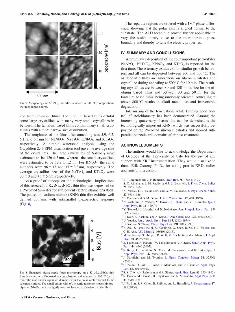
and tantalum-based films. The niobium based films exhibit
some large crystallites with many very small crystallites in
between. The tantalum based films contain many small crys-
tallites with a more narrow size distribution.
The roughness of the films after annealing was 5.9, 6.2,
5.1, and 6.5 nm for NaNbO3, NaTaO3, KNbO3, and KTaO3,
respectively. A simple watershed analysis using the
Gwyddion 2.43 SPM visualization tool gave the average size
of the crystallites. The large crystallites of NaNbO3 were
estimated to be 126 6 5 nm, whereas the small crystallites
were estimated to be 13.8 6 1.2 nm. For KNbO3, the same
numbers were 96 6 13 and 15 6 3.3 nm, respectively. The
average crystallite sizes of the NaTaO3 and KTaO3 were
33 6 3 and 43 6 5 nm, respectively.
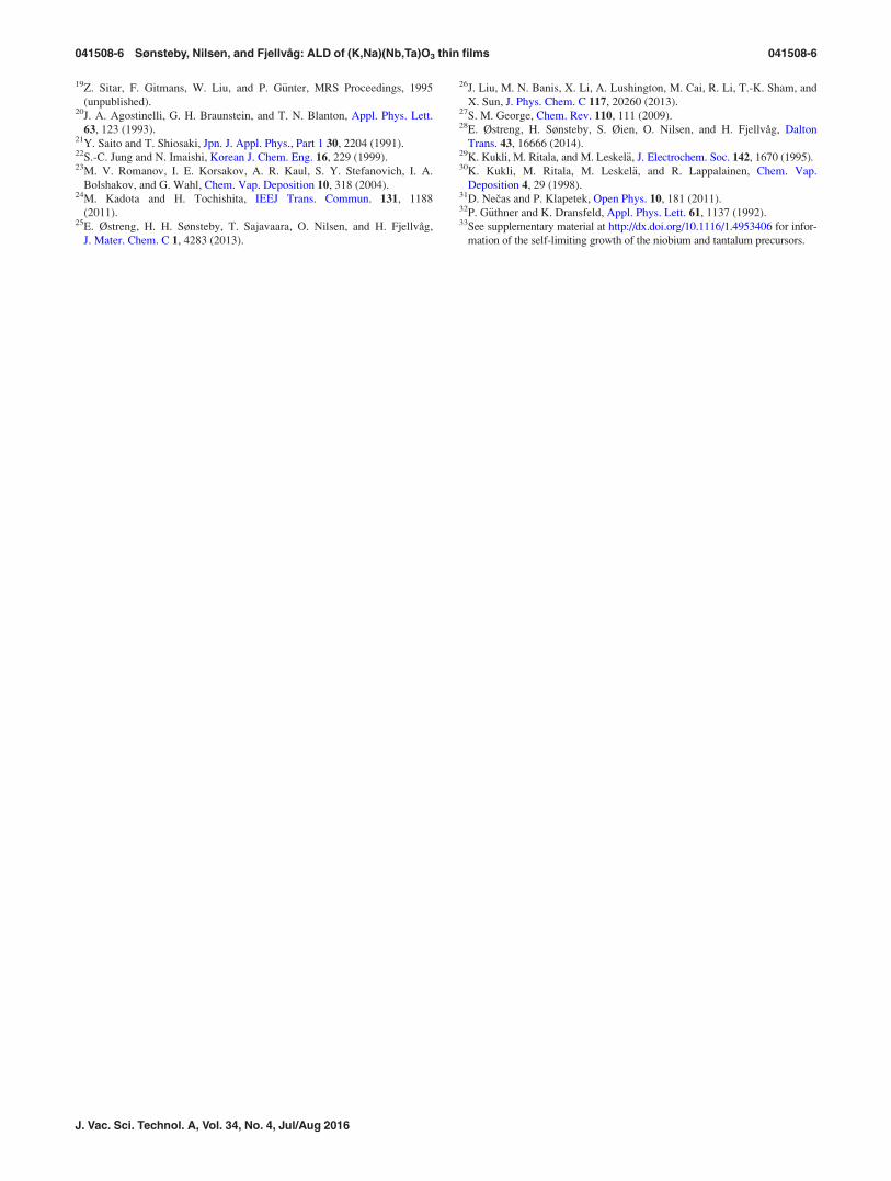
As a proof of concept on the technological implications
of this research, a K0.5Na0.5NbO3 thin film was deposited on
a Pt-coated Si-wafer for subsequent electric characterization.
The potassium sodium niobate (KNN) thin film exhibits well
defined domains with antiparallel piezoelectric response
(Fig. 8).
The separate regions are ordered with a 180� phase differ-
ence, showing that the polar axis is aligned normal to the
substrate. The ALD technique proved further applicable to
vary the stoichiometry close to the morphotropic phase
boundary and thereby to tune the electric properties.
IV. SUMMARY AND CONCLUSIONS
Atomic layer deposition of the four important perovskites
NaNbO3, NaTaO3, KNbO3, and KTaO3 is reported for the
first time. These ternary oxides exhibit similar growth behav-
iors and all can be deposited between 200 and 300 �C. The
as deposited films are amorphous on silicon substrates and
crystallize during annealing at 500 �C for 10 min. The result-
ing crystallites are between 80 and 180 nm in size for the ni-
obium based films and between 30 and 50 nm for the
tantalum based films, being randomly oriented. Annealing at
above 800 �C results in alkali metal loss and irreversible
degradation.
Intermixing of the four cations while keeping good con-
trol of stoichiometry has been demonstrated. Among the
interesting quaternary phases that can be deposited is the
technologically important KNN, which was successfully de-
posited on the Pt-coated silicon substrates and showed anti-
parallel piezoelectric domains after post-treatment.
ACKNOWLEDGMENTS
The authors would like to acknowledge the Department
of Geology at the University of Oslo for the use of and
support with XRF instrumentation. They would also like to
thank Erik Østreng, Ph.D., for taking part in XRD-studies
and fruitful discussion.
1B. T. Matthias and J. P. Remeika, Phys. Rev. 76, 1886 (1949).2S. C. Abrahams, J. M. Reddy, and J. L. Bernstein, J. Phys. Chem. Solids
27, 997 (1966).3K. Nassau, H. J. Levinstein, and G. M. Loiacono, J. Phys. Chem. Solids
27, 983 (1966).4L. Egerton and D. M. Dillon, J. Am. Ceram. Soc. 42, 438 (1959).5N. Yoshifumi, S. Wataru, M. Hiroshi, S. Tetsuo, and Y. Toshinobu, Jpn. J.
Appl. Phys. 46, 311 (2007).6Y. Tomoaki, I. Hiroshi, and N. Nobukazu, Jpn. J. Appl. Phys., Part 1 8,
1127 (1969).7H. Kato, K. Asakura, and A. Kudo, J. Am. Chem. Soc. 125, 3082 (2003).8U. Yutaka, Jpn. J. Appl. Phys., Part 1 13, 1362 (1974).9D. Xue and S. Zhang, Chem. Phys. Lett. 291, 401 (1998).
10K. Zou, S. Ismail-Beigi, K. Kisslinger, X. Shen, D. Su, F. J. Walker, and
C. H. Ahn, APL Mater. 3, 036104 (2015).11M. Sepliarsky, S. Phillpot, D. Wolf, M. Stachiotti, and R. Migoni, J. Appl.
Phys. 90, 4509 (2001).12S. Takehisa, A. Harumi, W. Takahiro, and A. Hideaki, Jpn. J. Appl. Phys.,
Part 1 44, 6969 (2005).13S. Kenji, O. Fumihito, N. Akira, M. Tomoyoshi, and K. Isaku, Jpn. J.
Appl. Phys., Part 1 47, 8909 (2008).14J. Narkilahti and M. Tyunina, J. Phys.: Condens. Matter 24, 325901
(2012).15C. Zaldo, D. Gill, R. Eason, J. Mendiola, and P. Chandler, Appl. Phys.
Lett. 65, 502 (1994).16S. S. Th€ony, H. Lehmann, and P. G€unter, Appl. Phys. Lett. 61, 373 (1992).17S. Takada, M. Ohnishi, H. Hayakawa, and N. Mikoshiba, Appl. Phys. Lett.
24, 490 (1974).18J.-W. Son, S. S. Orlov, B. Phillips, and L. Hesselink, J. Electroceram. 17,
591 (2006).
FIG. 7. Morphology of AIBVO3 thin films annealed at 500 �C; compositions
included in the figures.
FIG. 8. Enhanced piezoelectric force microscopy on a K0.5Na0.5NbO3 thin
film deposited on a Pt-coated silicon substrate and annealed at 500 �C for 10
min. The map shows separated domains with the polar vector normal to the
substrate surface. The small grains with 0 V electric response is possibly pre-
cipitated Nb2O5 due to a slightly overstoichiometry of niobium in the films.
041508-5 Sønsteby, Nilsen, and Fjellvag: ALD of (K,Na)(Nb,Ta)O3 thin films 041508-5
JVST A - Vacuum, Surfaces, and Films
19Z. Sitar, F. Gitmans, W. Liu, and P. G€unter, MRS Proceedings, 1995
(unpublished).20J. A. Agostinelli, G. H. Braunstein, and T. N. Blanton, Appl. Phys. Lett.
63, 123 (1993).21Y. Saito and T. Shiosaki, Jpn. J. Appl. Phys., Part 1 30, 2204 (1991).22S.-C. Jung and N. Imaishi, Korean J. Chem. Eng. 16, 229 (1999).23M. V. Romanov, I. E. Korsakov, A. R. Kaul, S. Y. Stefanovich, I. A.
Bolshakov, and G. Wahl, Chem. Vap. Deposition 10, 318 (2004).24M. Kadota and H. Tochishita, IEEJ Trans. Commun. 131, 1188
(2011).25E. Østreng, H. H. Sønsteby, T. Sajavaara, O. Nilsen, and H. Fjellvag,
J. Mater. Chem. C 1, 4283 (2013).
26J. Liu, M. N. Banis, X. Li, A. Lushington, M. Cai, R. Li, T.-K. Sham, and
X. Sun, J. Phys. Chem. C 117, 20260 (2013).27S. M. George, Chem. Rev. 110, 111 (2009).28E. Østreng, H. Sønsteby, S. Øien, O. Nilsen, and H. Fjellvag, Dalton
Trans. 43, 16666 (2014).29K. Kukli, M. Ritala, and M. Leskel€a, J. Electrochem. Soc. 142, 1670 (1995).30K. Kukli, M. Ritala, M. Leskel€a, and R. Lappalainen, Chem. Vap.
Deposition 4, 29 (1998).31D. Necas and P. Klapetek, Open Phys. 10, 181 (2011).32P. G€uthner and K. Dransfeld, Appl. Phys. Lett. 61, 1137 (1992).33See supplementary material at http://dx.doi.org/10.1116/1.4953406 for infor-
mation of the self-limiting growth of the niobium and tantalum precursors.
041508-6 Sønsteby, Nilsen, and Fjellvag: ALD of (K,Na)(Nb,Ta)O3 thin films 041508-6
J. Vac. Sci. Technol. A, Vol. 34, No. 4, Jul/Aug 2016