at89c51cc01 datasheet enhanced 8-bit mcu with can ... · pdf file• boot code section with...
TRANSCRIPT

Rev. 4129N–CAN–03/08
1
Features• 80C51 Core Architecture
• 256 Bytes of On-chip RAM
• 1K Bytes of On-chip XRAM
• 32K Bytes of On-chip Flash Memory
– Data Retention: 10 Years at 85°C
Erase/Write Cycle: 100K
• Boot Code Section with Independent Lock Bits
• 2K Bytes of On-chip Flash for Bootloader
• In-System Programming by On-Chip Boot Program (CAN, UART) and IAP Capability
• 2K Bytes of On-chip EEPROM
Erase/Write Cycle: 100K
• 14-sources 4-level Interrupts
• Three 16-bit Timers/Counters
• Full Duplex UART Compatible 80C51
• Maximum Crystal Frequency 40 MHz, in X2 Mode, 20 MHz (CPU Core, 20 MHz)
• Five Ports: 32 + 2 Digital I/O Lines
• Five-channel 16-bit PCA with:
– PWM (8-bit)
– High-speed Output
– Timer and Edge Capture
• Double Data Pointer
• 21-bit Watchdog Timer (7 Programmable Bits)
• A 10-bit Resolution Analog to Digital Converter (ADC) with 8 Multiplexed Inputs
• Full CAN Controller:
– Fully Compliant with CAN Rev2.0A and 2.0B
– Optimized Structure for Communication Management (Via SFR)
– 15 Independent Message Objects:
Each Message Object Programmable on Transmission or Reception
Individual Tag and Mask Filters up to 29-bit Identifier/Channel
8-byte Cyclic Data Register (FIFO)/Message Object
16-bit Status and Control Register/Message Object
16-bit Time-Stamping Register/Message Object
CAN Specification 2.0 Part A or 2.0 Part B Programmable for Each Message
Object
Access to Message Object Control and Data Registers Via SFR
Programmable Reception Buffer Length Up To 15 Message Objects
Priority Management of Reception of Hits on Several Message Objects at the
Same Time (Basic CAN Feature)
Priority Management for Transmission
Message Object Overrun Interrupt
– Supports:
Time Triggered Communication
Autobaud and Listening Mode
Programmable Automatic Reply Mode
– 1-Mbit/s Maximum Transfer Rate at 8 MHz (1) Crystal Frequency in X2 Mode
– Readable Error Counters
– Programmable Link to On-chip Timer for Time Stamping and Network
Synchronization
– Independent Baud Rate Prescaler
– Data, Remote, Error and Overload Frame Handling
• On-chip Emulation Logic (Enhanced Hook System)
• Power Saving Modes:
– Idle Mode
– Power-down Mode
1. At BRP = 1 sampling point will be fixed.
Enhanced 8-bit
Microcontroller
with CAN
Controller and
Flash Memory
T89C51CC01
AT89C51CC01

2 A/T89C51CC014129N–CAN–03/08
• Power Supply: 3V to 5.5V
• Temperature Range: Industrial (-40° to +85°C)
• Packages: VQFP44, PLCC44
Description The T89C51CC01 is the first member of the CANaryTM family of 8-bit microcontrollers
dedicated to CAN network applications.
In X2 mode a maximum external clock rate of 20 MHz reaches a 300 ns cycle time.
Besides the full CAN controller T89C51CC01 provides 32K Bytes of Flash memory
including In-System-Programming (ISP), 2K Bytes Boot Flash Memory, 2K Bytes
EEPROM and 1.2-Kbyte RAM.
Special attention is paid to the reduction of the electro-magnetic emission of
T89C51CC01.
Block Diagram
Notes: 1. 8 analog Inputs/8 Digital I/O
2. 2-Bit I/O Port
Timer 0 INT
RAM256x8
T0
T1
RxD
TxD
WR
RD
EA
PSEN
ALE
XTAL2
XTAL1
UART
CPU
Timer 1
INT
1
Ctrl
INT
0
C51 CORE
Port 0
P0
Port 1 Port 2 Port 3
Parallel I/O Ports and Ext. Bus
P1(1
)
P2
P3
XRAM1kx8
IB-bus
PCA
RE
SE
T
WatchDog
PC
A
EC
I
Vss
Vcc
Timer 2
T2E
X
T2
Port 4
P4(2
)
10 bitADC
Flash32kx
8
Bootloader2kx8
EEPROM2kx8
CAN
CONTROLLER
TxD
C
Rx
DC
VA
RE
F
VA
VC
C
VA
GN
D

3
A/T89C51CC01
4129N–CAN–03/08
Pin Configuration
PLCC44
P1
.3/A
N3
/CE
X0
P1
.2/A
N2
/EC
I
P1
.1/A
N1
/T2
EX
P1
.0/A
N 0
/T2
VA
RE
F
VA
GN
D
RE
SE
T
VS
S
VC
C
XT
AL
1
XT
AL
2
P3
.7/R
D
P4
.0/
Tx
DC
P4
.1/R
xD
C
P2
.7/A
15
P2
.6/A
14
P2
.5/A
13
P2
.4/A
12
P2
.3/A
11
P2
.2/A
10
P2
.1/A
9
P3
.6/W
R
39
38
37
36
35
34
33
32
29
30
31
7
8
9
10
11
12
13
14
17
16
15
18
19
20
21
22
23
24
25
26
27
28
6 5 4 3 2
44
43
42
41
40
ALE
PSEN
P0.7/AD7
P0.6/AD6
P0.5/AD5
P0.2/AD2
P0.3/AD3
P0.4/AD4
P0.1/AD1
P0.0/AD0
P2.0/A8
P1.4/AN4/CEX1
P1.5/AN5/CEX2
P1.6/AN6/CEX3
P1.7/AN7/CEX4
EA
P3.0/RxD
P3.1/TxD
P3.2/INT0
P3.3/INT1
P3.4/T0
P3.5/T1
1
43 42 41 40 3944 38 37 36 35 34
12 13 17161514 201918 21 22
33
32
31
30
29
28
27
26
25
24
23
VQFP44
1
2
3
4
5
6
7
8
9
10
11
P1.4/AN4/CEX1
P1.5/AN5/CEX2
P1.6/AN6/CEX3
P1.7/AN7/CEX4
EA
P3.0/RxD
P3.1/TxD
P3.2/INT0
P3.3/INT1
P3.4/T0
P3.5/T1
ALE
PSEN
P0.7/AD7
P0.6/AD6
P0.5/AD5
P0.2 /AD2
P0.3 /AD3
P0.4 /AD4
P0.1 /AD1
P0.0 /AD0
P2.0/A8
P1
.3/A
N3
/CE
X0
P1
.2/A
N2
/EC
I
P1
.1/A
N1
/T2
EX
P1
.0/A
N 0
/T2
VA
RE
F
VA
GN
D
RE
SE
T
VS
S
VC
C
XT
AL
1
XT
AL
2
P3
.7/R
D
P4
.0/T
xD
C
P4
.1/R
xD
C
P2
.7/A
15
P2
.6/A
14
P2
.5/A
13
P2
.4/A
12
P2
.3/A
11
P2
.2/A
10
P2
.1/A
9
P3
.6/W
R

4 A/T89C51CC014129N–CAN–03/08
I/O Configurations Each Port SFR operates via type-D latches, as illustrated in Figure 1 for Ports 3 and 4. A
CPU "write to latch" signal initiates transfer of internal bus data into the type-D latch. A
CPU "read latch" signal transfers the latched Q output onto the internal bus. Similarly, a
"read pin" signal transfers the logical level of the Port pin. Some Port data instructions
activate the "read latch" signal while others activate the "read pin" signal. Latch instruc-
tions are referred to as Read-Modify-Write instructions. Each I/O line may be
independently programmed as input or output.
Port 1, Port 3 and Port 4 Figure 1 shows the structure of Ports 1 and 3, which have internal pull-ups. An external
source can pull the pin low. Each Port pin can be configured either for general-purpose
I/O or for its alternate input output function.
To use a pin for general-purpose output, set or clear the corresponding bit in the Px reg-
ister (x = 1,3 or 4). To use a pin for general-purpose input, set the bit in the Px register.
This turns off the output FET drive.
To configure a pin for its alternate function, set the bit in the Px register. When the latch
is set, the "alternate output function" signal controls the output level (see Figure 1). The
operation of Ports 1, 3 and 4 is discussed further in the "quasi-Bidirectional Port Opera-
tion" section.
Figure 1. Port 1, Port 3 and Port 4 Structure
Note: The internal pull-up can be disabled on P1 when analog function is selected.
Port 0 and Port 2 Ports 0 and 2 are used for general-purpose I/O or as the external address/data bus. Port
0, shown in Figure 3, differs from the other Ports in not having internal pull-ups. Figure 3
shows the structure of Port 2. An external source can pull a Port 2 pin low.
To use a pin for general-purpose output, set or clear the corresponding bit in the Px reg-
ister (x = 0 or 2). To use a pin for general-purpose input, set the bit in the Px register to
turn off the output driver FET.
D
CL
QP1.X
LATCH
INTERNAL
WRITETOLATCH
READPIN
READLATCH
P1.x
P3.XP4.X
ALTERNATEOUTPUTFUNCTION
VCC
INTERNALPULL-UP (1)
ALTERNATEINPUTFUNCTION
P3.xP4.x
BUS
5
A/T89C51CC01
4129N–CAN–03/08
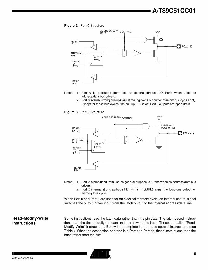
Figure 2. Port 0 Structure
Notes: 1. Port 0 is precluded from use as general-purpose I/O Ports when used as
address/data bus drivers.
2. Port 0 internal strong pull-ups assist the logic-one output for memory bus cycles only.
Except for these bus cycles, the pull-up FET is off, Port 0 outputs are open-drain.
Figure 3. Port 2 Structure
Notes: 1. Port 2 is precluded from use as general-purpose I/O Ports when as address/data bus
drivers.
2. Port 2 internal strong pull-ups FET (P1 in FiGURE) assist the logic-one output for
memory bus cycle.
When Port 0 and Port 2 are used for an external memory cycle, an internal control signal
switches the output-driver input from the latch output to the internal address/data line.
Read-Modify-Write Instructions
Some instructions read the latch data rather than the pin data. The latch based instruc-
tions read the data, modify the data and then rewrite the latch. These are called "Read-
Modify-Write" instructions. Below is a complete list of these special instructions (see
Table ). When the destination operand is a Port or a Port bit, these instructions read the
latch rather than the pin:
D QP0.X
LATCH
INTERNAL
WRITETOLATCH
READPIN
READLATCH
0
1
P0.x (1)
ADDRESS LOW/DATA
CONTROL VDD
BUS
(2)
D QP2.X
LATCH
INTERNAL
WRITETOLATCH
READPIN
READLATCH
0
1
P2.x (1)
ADDRESS HIGH/ CONTROL
BUS
VDD
INTERNALPULL-UP (2)

6 A/T89C51CC014129N–CAN–03/08
It is not obvious the last three instructions in this list are Read-Modify-Write instructions.
These instructions read the port (all 8 bits), modify the specifically addressed bit and
write the new byte back to the latch. These Read-Modify-Write instructions are directed
to the latch rather than the pin in order to avoid possible misinterpretation of voltage
(and therefore, logic) levels at the pin. For example, a Port bit used to drive the base of
an external bipolar transistor can not rise above the transistor’s base-emitter junction
voltage (a value lower than VIL). With a logic one written to the bit, attempts by the CPU
to read the Port at the pin are misinterpreted as logic zero. A read of the latch rather
than the pins returns the correct logic-one value.
Quasi-Bidirectional Port Operation
Port 1, Port 2, Port 3 and Port 4 have fixed internal pull-ups and are referred to as
"quasi-bidirectional" Ports. When configured as an input, the pin impedance appears as
logic one and sources current in response to an external logic zero condition. Port 0 is a
"true bidirectional" pin. The pins float when configured as input. Resets write logic one to
all Port latches. If logical zero is subsequently written to a Port latch, it can be returned
to input conditions by a logical one written to the latch.
Note: Port latch values change near the end of Read-Modify-Write instruction cycles. Output
buffers (and therefore the pin state) update early in the instruction after Read-Modify-
Write instruction cycle.
Logical zero-to-one transitions in Port 1, Port 2, Port 3 and Port 4 use an additional pull-
up (p1) to aid this logic transition (see Figure 4.). This increases switch speed. This
extra pull-up sources 100 times normal internal circuit current during 2 oscillator clock
periods. The internal pull-ups are field-effect transistors rather than linear resistors. Pull-
ups consist of three p-channel FET (pFET) devices. A pFET is on when the gate senses
logical zero and off when the gate senses logical one. pFET #1 is turned on for two
oscillator periods immediately after a zero-to-one transition in the Port latch. A logical
one at the Port pin turns on pFET #3 (a weak pull-up) through the inverter. This inverter
and pFET pair form a latch to drive logical one. pFET #2 is a very weak pull-up switched
on whenever the associated nFET is switched off. This is traditional CMOS switch con-
vention. Current strengths are 1/10 that of pFET #3.
Table 1. Read-Modify-Write Instructions
Instruction Description Example
ANL logical AND ANL P1, A
ORL logical OR ORL P2, A
XRL logical EX-OR XRL P3, A
JBC jump if bit = 1 and clear bit JBC P1.1, LABEL
CPL complement bit CPL P3.0
INC increment INC P2
DEC decrement DEC P2
DJNZ decrement and jump if not zero DJNZ P3, LABEL
MOV Px.y, C move carry bit to bit y of Port x MOV P1.5, C
CLR Px.y clear bit y of Port x CLR P2.4
SET Px.y set bit y of Port x SET P3.3

7
A/T89C51CC01
4129N–CAN–03/08
Figure 4. Internal Pull-Up Configurations
Note: Port 2 p1 assists the logic-one output for memory bus cycles.
READ PIN
INPUT DATA
P1.x
OUTPUT DATA
2 Osc. PERIODS
n
p1(1) p2 p3
VCCVCCVCC
P2.xP3.xP4.x
8 A/T89C51CC014129N–CAN–03/08
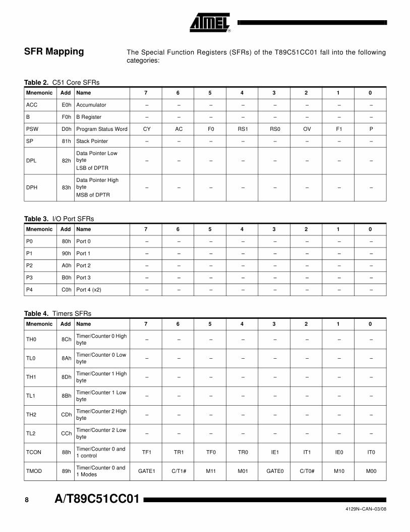
SFR Mapping The Special Function Registers (SFRs) of the T89C51CC01 fall into the following
categories:
Table 2. C51 Core SFRs
Mnemonic Add Name 7 6 5 4 3 2 1 0
ACC E0h Accumulator – – – – – – – –
B F0h B Register – – – – – – – –
PSW D0h Program Status Word CY AC F0 RS1 RS0 OV F1 P
SP 81h Stack Pointer – – – – – – – –
DPL 82h
Data Pointer Low
byte
LSB of DPTR
– – – – – – – –
DPH 83h
Data Pointer High
byte
MSB of DPTR
– – – – – – – –
Table 3. I/O Port SFRs
Mnemonic Add Name 7 6 5 4 3 2 1 0
P0 80h Port 0 – – – – – – – –
P1 90h Port 1 – – – – – – – –
P2 A0h Port 2 – – – – – – – –
P3 B0h Port 3 – – – – – – – –
P4 C0h Port 4 (x2) – – – – – – – –
Table 4. Timers SFRs
Mnemonic Add Name 7 6 5 4 3 2 1 0
TH0 8ChTimer/Counter 0 High
byte– – – – – – – –
TL0 8AhTimer/Counter 0 Low
byte– – – – – – – –
TH1 8DhTimer/Counter 1 High
byte– – – – – – – –
TL1 8BhTimer/Counter 1 Low
byte– – – – – – – –
TH2 CDhTimer/Counter 2 High
byte– – – – – – – –
TL2 CChTimer/Counter 2 Low
byte– – – – – – – –
TCON 88hTimer/Counter 0 and
1 controlTF1 TR1 TF0 TR0 IE1 IT1 IE0 IT0
TMOD 89hTimer/Counter 0 and
1 ModesGATE1 C/T1# M11 M01 GATE0 C/T0# M10 M00
9
A/T89C51CC01
4129N–CAN–03/08
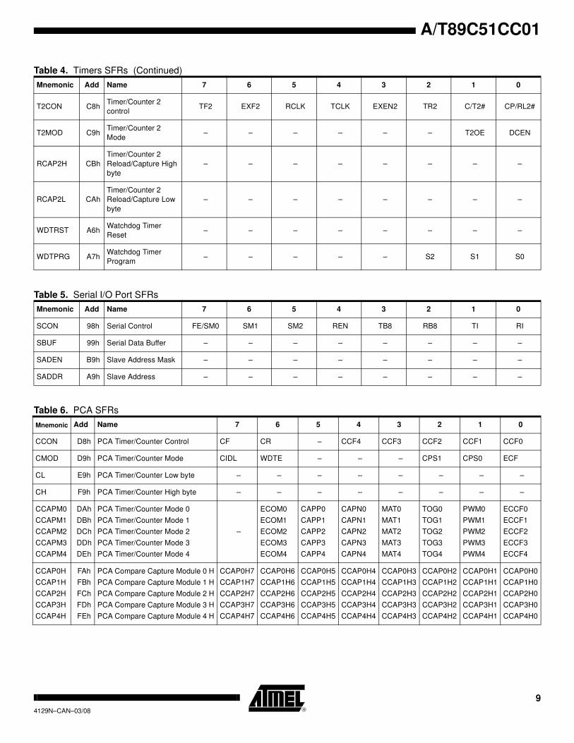
T2CON C8hTimer/Counter 2
controlTF2 EXF2 RCLK TCLK EXEN2 TR2 C/T2# CP/RL2#
T2MOD C9hTimer/Counter 2
Mode– – – – – – T2OE DCEN
RCAP2H CBh
Timer/Counter 2
Reload/Capture High
byte
– – – – – – – –
RCAP2L CAh
Timer/Counter 2
Reload/Capture Low
byte
– – – – – – – –
WDTRST A6hWatchdog Timer
Reset– – – – – – – –
WDTPRG A7hWatchdog Timer
Program– – – – – S2 S1 S0
Table 4. Timers SFRs (Continued)
Mnemonic Add Name 7 6 5 4 3 2 1 0
Table 5. Serial I/O Port SFRs
Mnemonic Add Name 7 6 5 4 3 2 1 0
SCON 98h Serial Control FE/SM0 SM1 SM2 REN TB8 RB8 TI RI
SBUF 99h Serial Data Buffer – – – – – – – –
SADEN B9h Slave Address Mask – – – – – – – –
SADDR A9h Slave Address – – – – – – – –
Table 6. PCA SFRs
Mnemonic Add Name 7 6 5 4 3 2 1 0
CCON D8h PCA Timer/Counter Control CF CR – CCF4 CCF3 CCF2 CCF1 CCF0
CMOD D9h PCA Timer/Counter Mode CIDL WDTE – – – CPS1 CPS0 ECF
CL E9h PCA Timer/Counter Low byte – – – – – – – –
CH F9h PCA Timer/Counter High byte – – – – – – – –
CCAPM0
CCAPM1
CCAPM2
CCAPM3
CCAPM4
DAh
DBh
DCh
DDh
DEh
PCA Timer/Counter Mode 0
PCA Timer/Counter Mode 1
PCA Timer/Counter Mode 2
PCA Timer/Counter Mode 3
PCA Timer/Counter Mode 4
–
ECOM0
ECOM1
ECOM2
ECOM3
ECOM4
CAPP0
CAPP1
CAPP2
CAPP3
CAPP4
CAPN0
CAPN1
CAPN2
CAPN3
CAPN4
MAT0
MAT1
MAT2
MAT3
MAT4
TOG0
TOG1
TOG2
TOG3
TOG4
PWM0
PWM1
PWM2
PWM3
PWM4
ECCF0
ECCF1
ECCF2
ECCF3
ECCF4
CCAP0H
CCAP1H
CCAP2H
CCAP3H
CCAP4H
FAh
FBh
FCh
FDh
FEh
PCA Compare Capture Module 0 H
PCA Compare Capture Module 1 H
PCA Compare Capture Module 2 H
PCA Compare Capture Module 3 H
PCA Compare Capture Module 4 H
CCAP0H7
CCAP1H7
CCAP2H7
CCAP3H7
CCAP4H7
CCAP0H6
CCAP1H6
CCAP2H6
CCAP3H6
CCAP4H6
CCAP0H5
CCAP1H5
CCAP2H5
CCAP3H5
CCAP4H5
CCAP0H4
CCAP1H4
CCAP2H4
CCAP3H4
CCAP4H4
CCAP0H3
CCAP1H3
CCAP2H3
CCAP3H3
CCAP4H3
CCAP0H2
CCAP1H2
CCAP2H2
CCAP3H2
CCAP4H2
CCAP0H1
CCAP1H1
CCAP2H1
CCAP3H1
CCAP4H1
CCAP0H0
CCAP1H0
CCAP2H0
CCAP3H0
CCAP4H0
10 A/T89C51CC014129N–CAN–03/08
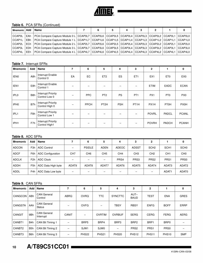
CCAP0L
CCAP1L
CCAP2L
CCAP3L
CCAP4L
EAh
EBh
ECh
EDh
EEh
PCA Compare Capture Module 0 L
PCA Compare Capture Module 1 L
PCA Compare Capture Module 2 L
PCA Compare Capture Module 3 L
PCA Compare Capture Module 4 L
CCAP0L7
CCAP1L7
CCAP2L7
CCAP3L7
CCAP4L7
CCAP0L6
CCAP1L6
CCAP2L6
CCAP3L6
CCAP4L6
CCAP0L5
CCAP1L5
CCAP2L5
CCAP3L5
CCAP4L5
CCAP0L4
CCAP1L4
CCAP2L4
CCAP3L4
CCAP4L4
CCAP0L3
CCAP1L3
CCAP2L3
CCAP3L3
CCAP4L3
CCAP0L2
CCAP1L2
CCAP2L2
CCAP3L2
CCAP4L2
CCAP0L1
CCAP1L1
CCAP2L1
CCAP3L1
CCAP4L1
CCAP0L0
CCAP1L0
CCAP2L0
CCAP3L0
CCAP4L0
Table 6. PCA SFRs (Continued)
Mnemonic Add Name 7 6 5 4 3 2 1 0
Table 7. Interrupt SFRs
Mnemonic Add Name 7 6 5 4 3 2 1 0
IEN0 A8hInterrupt Enable
Control 0EA EC ET2 ES ET1 EX1 ET0 EX0
IEN1 E8hInterrupt Enable
Control 1– – – – – ETIM EADC ECAN
IPL0 B8hInterrupt Priority
Control Low 0– PPC PT2 PS PT1 PX1 PT0 PX0
IPH0 B7hInterrupt Priority
Control High 0– PPCH PT2H PSH PT1H PX1H PT0H PX0H
IPL1 F8hInterrupt Priority
Control Low 1– – – – – POVRL PADCL PCANL
IPH1 F7hInterrupt Priority
Control High1– – – – – POVRH PADCH PCANH
Table 8. ADC SFRs
Mnemonic Add Name 7 6 5 4 3 2 1 0
ADCON F3h ADC Control – PSIDLE ADEN ADEOC ADSST SCH2 SCH1 SCH0
ADCF F6h ADC Configuration CH7 CH6 CH5 CH4 CH3 CH2 CH1 CH0
ADCLK F2h ADC Clock – – – PRS4 PRS3 PRS2 PRS1 PRS0
ADDH F5h ADC Data High byte ADAT9 ADAT8 ADAT7 ADAT6 ADAT5 ADAT4 ADAT3 ADAT2
ADDL F4h ADC Data Low byte – – – – – – ADAT1 ADAT0
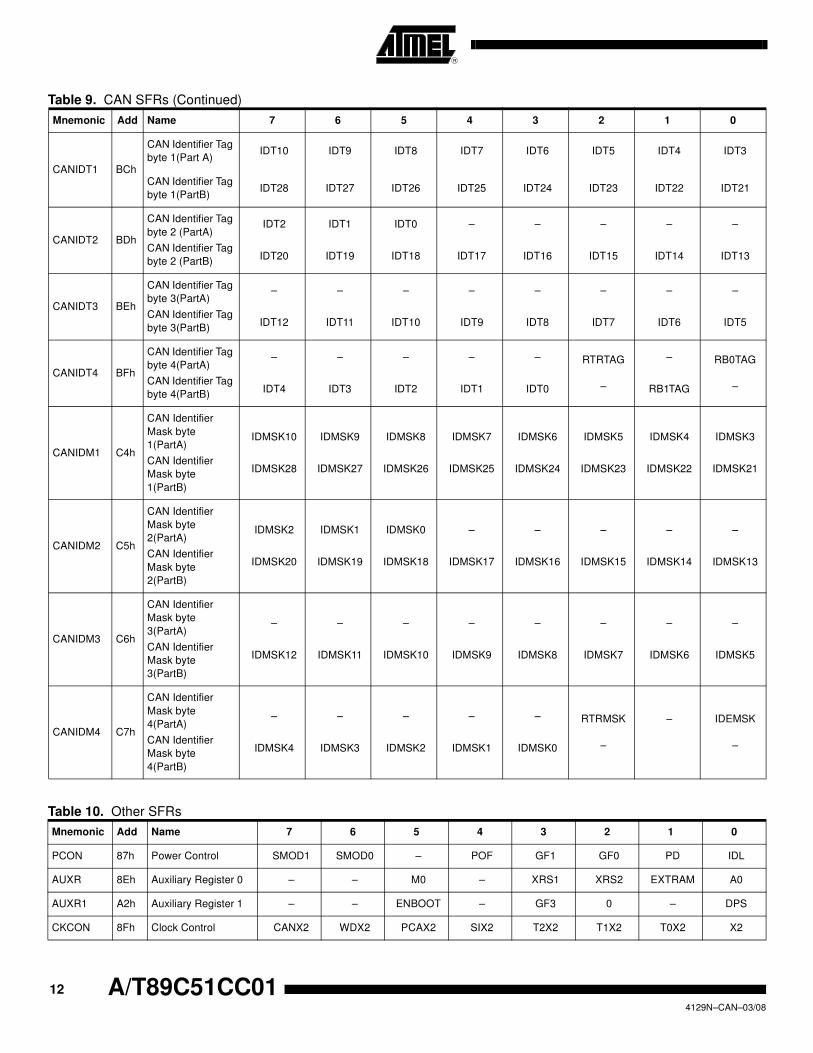
Table 9. CAN SFRs
Mnemonic Add Name 7 6 5 4 3 2 1 0
CANGCON ABhCAN General
ControlABRQ OVRQ TTC SYNCTTC
AUT–
BAUDTEST ENA GRES
CANGSTA AAhCAN General
Status– OVFG – TBSY RBSY ENFG BOFF ERRP
CANGIT 9BhCAN General
InterruptCANIT – OVRTIM OVRBUF SERG CERG FERG AERG
CANBT1 B4h CAN Bit Timing 1 – BRP5 BRP4 BRP3 BRP2 BRP1 BRP0 –
CANBT2 B5h CAN Bit Timing 2 – SJW1 SJW0 – PRS2 PRS1 PRS0 –
CANBT3 B6h CAN Bit Timing 3 – PHS22 PHS21 PHS20 PHS12 PHS11 PHS10 SMP

11
A/T89C51CC01
4129N–CAN–03/08
CANEN1 CEhCAN Enable
Channel byte 1– ENCH14 ENCH13 ENCH12 ENCH11 ENCH10 ENCH9 ENCH8
CANEN2 CFhCAN Enable
Channel byte 2ENCH7 ENCH6 ENCH5 ENCH4 ENCH3 ENCH2 ENCH1 ENCH0
CANGIE C1hCAN General
Interrupt Enable– – ENRX ENTX ENERCH ENBUF ENERG –
CANIE1 C2h
CAN Interrupt
Enable Channel
byte 1
– IECH14 IECH13 IECH12 IECH11 IECH10 IECH9 IECH8
CANIE2 C3h
CAN Interrupt
Enable Channel
byte 2
IECH7 IECH6 IECH5 IECH4 IECH3 IECH2 IECH1 IECH0
CANSIT1 BAh
CAN Status
Interrupt Channel
byte1
– SIT14 SIT13 SIT12 SIT11 SIT10 SIT9 SIT8
CANSIT2 BBh
CAN Status
Interrupt Channel
byte2
SIT7 SIT6 SIT5 SIT4 SIT3 SIT2 SIT1 SIT0
CANTCON A1hCAN Timer
ControlTPRESC 7 TPRESC 6 TPRESC 5 TPRESC 4 TPRESC 3 TPRESC 2 TPRESC 1 TPRESC 0
CANTIMH ADh CAN Timer highCANTIM
15
CANTIM
14
CANTIM
13
CANTIM
12
CANTIM
11
CANTIM
10
CANTIM
9
CANTIM
8
CANTIML ACh CAN Timer low CANTIM 7 CANTIM 6 CANTIM 5 CANTIM 4 CANTIM 3 CANTIM 2 CANTIM 1 CANTIM 0
CANSTMH AFhCAN Timer Stamp
high
TIMSTMP
15
TIMSTMP
14
TIMSTMP
13
TIMSTMP
12
TIMSTMP
11
TIMSTMP
10
TIMSTMP
9
TIMSTMP
8
CANSTML AEhCAN Timer Stamp
low
TIMSTMP
7
TIMSTMP
6
TIMSTMP
5
TIMSTMP
4
TIMSTMP
3
TIMSTMP
2
TIMSTMP
1
TIMSTMP
0
CANTTCH A5hCAN Timer TTC
highTIMTTC 15 TIMTTC 14 TIMTTC 13 TIMTTC 12 TIMTTC 11 TIMTTC 10 TIMTTC 9 TIMTTC 8
CANTTCL A4hCAN Timer TTC
low
TIMTTC
7
TIMTTC
6
TIMTTC
5
TIMTTC
4
TIMTTC
3
TIMTTC
2
TIMTTC
1
TIMTTC
0
CANTEC 9ChCAN Transmit
Error CounterTEC7 TEC6 TEC5 TEC4 TEC3 TEC2 TEC1 TEC0
CANREC 9DhCAN Receive
Error CounterREC7 REC6 REC5 REC4 REC3 REC2 REC1 REC0
CANPAGE B1h CAN Page CHNB3 CHNB2 CHNB1 CHNB0 AINC INDX2 INDX1 INDX0
CANSTCH B2hCAN Status
ChannelDLCW TXOK RXOK BERR SERR CERR FERR AERR
CANCONH B3hCAN Control
ChannelCONCH1 CONCH0 RPLV IDE DLC3 DLC2 DLC1 DLC0
CANMSG A3hCAN Message
DataMSG7 MSG6 MSG5 MSG4 MSG3 MSG2 MSG1 MSG0
Table 9. CAN SFRs (Continued)
Mnemonic Add Name 7 6 5 4 3 2 1 0
12 A/T89C51CC014129N–CAN–03/08
CANIDT1 BCh
CAN Identifier Tag
byte 1(Part A)IDT10 IDT9 IDT8 IDT7 IDT6 IDT5 IDT4 IDT3
CAN Identifier Tag
byte 1(PartB)IDT28 IDT27 IDT26 IDT25 IDT24 IDT23 IDT22 IDT21
CANIDT2 BDh
CAN Identifier Tag
byte 2 (PartA)
CAN Identifier Tag
byte 2 (PartB)
IDT2
IDT20
IDT1
IDT19
IDT0
IDT18
–
IDT17
–
IDT16
–
IDT15
–
IDT14
–
IDT13
CANIDT3 BEh
CAN Identifier Tag
byte 3(PartA)
CAN Identifier Tag
byte 3(PartB)
–
IDT12
–
IDT11
–
IDT10
–
IDT9
–
IDT8
–
IDT7
–
IDT6
–
IDT5
CANIDT4 BFh
CAN Identifier Tag
byte 4(PartA)
CAN Identifier Tag
byte 4(PartB)
–
IDT4
–
IDT3
–
IDT2
–
IDT1
–
IDT0
RTRTAG
–
–
RB1TAG
RB0TAG
–
CANIDM1 C4h
CAN Identifier
Mask byte
1(PartA)
CAN Identifier
Mask byte
1(PartB)
IDMSK10
IDMSK28
IDMSK9
IDMSK27
IDMSK8
IDMSK26
IDMSK7
IDMSK25
IDMSK6
IDMSK24
IDMSK5
IDMSK23
IDMSK4
IDMSK22
IDMSK3
IDMSK21
CANIDM2 C5h
CAN Identifier
Mask byte
2(PartA)
CAN Identifier
Mask byte
2(PartB)
IDMSK2
IDMSK20
IDMSK1
IDMSK19
IDMSK0
IDMSK18
–
IDMSK17
–
IDMSK16
–
IDMSK15
–
IDMSK14
–
IDMSK13
CANIDM3 C6h
CAN Identifier
Mask byte
3(PartA)
CAN Identifier
Mask byte
3(PartB)
–
IDMSK12
–
IDMSK11
–
IDMSK10
–
IDMSK9
–
IDMSK8
–
IDMSK7
–
IDMSK6
–
IDMSK5
CANIDM4 C7h
CAN Identifier
Mask byte
4(PartA)
CAN Identifier
Mask byte
4(PartB)
–
IDMSK4
–
IDMSK3
–
IDMSK2
–
IDMSK1
–
IDMSK0
RTRMSK
–
– IDEMSK
–
Table 9. CAN SFRs (Continued)
Mnemonic Add Name 7 6 5 4 3 2 1 0
Table 10. Other SFRs
Mnemonic Add Name 7 6 5 4 3 2 1 0
PCON 87h Power Control SMOD1 SMOD0 – POF GF1 GF0 PD IDL
AUXR 8Eh Auxiliary Register 0 – – M0 – XRS1 XRS2 EXTRAM A0
AUXR1 A2h Auxiliary Register 1 – – ENBOOT – GF3 0 – DPS
CKCON 8Fh Clock Control CANX2 WDX2 PCAX2 SIX2 T2X2 T1X2 T0X2 X2

13
A/T89C51CC01
4129N–CAN–03/08
Reserved
Note: 1. These registers are bit–addressable.
Sixteen addresses in the SFR space are both byte–addressable and bit–addressable. The bit–addressable SFR’s are those
whose address ends in 0 and 8. The bit addresses, in this area, are 0x80 through to 0xFF.
FCON D1h Flash Control FPL3 FPL2 FPL1 FPL0 FPS FMOD1 FMOD0 FBUSY
EECON D2h EEPROM Contol EEPL3 EEPL2 EEPL1 EEPL0 – – EEE EEBUSY
Table 10. Other SFRs
Mnemonic Add Name 7 6 5 4 3 2 1 0
Table 11. SFR Mapping
0/8(1) 1/9 2/A 3/B 4/C 5/D 6/E 7/F
F8hIPL1
xxxx x000
CH
0000 0000
CCAP0H
0000 0000
CCAP1H
0000 0000
CCAP2H
0000 0000
CCAP3H
0000 0000
CCAP4H
0000 0000FFh
F0hB
0000 0000
ADCLK
xxx0 0000
ADCON
x000 0000
ADDL
0000 0000
ADDH
0000 0000
ADCF
0000 0000
IPH1
xxxx x000F7h
E8hIEN1
xxxx x000
CL
0000 0000
CCAP0L
0000 0000
CCAP1L
0000 0000
CCAP2L
0000 0000
CCAP3L
0000 0000
CCAP4L
0000 0000EFh
E0hACC
0000 0000E7h
D8hCCON
00x0 0000
CMOD
00xx x000
CCAPM0
x000 0000
CCAPM1
x000 0000
CCAPM2
x000 0000
CCAPM3
x000 0000
CCAPM4
x000 0000DFh
D0hPSW
0000 0000
FCON
0000 0000
EECON
xxxx xx00D7h
C8hT2CON
0000 0000
T2MOD
xxxx xx00
RCAP2L
0000 0000
RCAP2H
0000 0000
TL2
0000 0000
TH2
0000 0000
CANEN1
x000 0000
CANEN2
0000 0000CFh
C0hP4
xxxx xx11
CANGIE
1100 0000
CANIE1
x000 0000
CANIE2
0000 0000
CANIDM1
xxxx xxxx
CANIDM2
xxxx xxxx
CANIDM3
xxxx xxxx
CANIDM4
xxxx xxxxC7h
B8hIPL0
x000 0000
SADEN
0000 0000
CANSIT1
x000 0000
CANSIT2
0000 0000
CANIDT1
xxxx xxxx
CANIDT2
xxxx xxxx
CANIDT3
xxxx xxxx
CANIDT4
xxxx xxxxBFh
B0hP3
1111 1111
CANPAGE
0000 0000
CANSTCH
xxxx xxxx
CANCONCH
xxxx xxxx
CANBT1
xxxx xxxx
CANBT2
xxxx xxxx
CANBT3
xxxx xxxx
IPH0
x000 0000B7h
A8hIEN0
0000 0000
SADDR
0000 0000
CANGSTA
1010 0000
CANGCON
0000 0000
CANTIML
0000 0000
CANTIMH
0000 0000
CANSTMPL
xxxx xxxx
CANSTMPH
xxxx xxxxAFh
A0hP2
1111 1111
CANTCON
0000 0000
AUXR1
xxxx 00x0
CANMSG
xxxx xxxx
CANTTCL
0000 0000
CANTTCH
0000 0000
WDTRST
1111 1111
WDTPRG
xxxx x000A7h
98hSCON
0000 0000
SBUF
0000 0000
CANGIT
0x00 0000
CANTEC
0000 0000
CANREC
0000 00009Fh
90hP1
1111 111197h
88hTCON
0000 0000
TMOD
0000 0000
TL0
0000 0000
TL1
0000 0000
TH0
0000 0000
TH1
0000 0000
AUXR
x00x 1100
CKCON
0000 00008Fh
80hP0
1111 1111
SP
0000 0111
DPL
0000 0000
DPH
0000 0000
PCON
00x1 000087h
0/8(1) 1/9 2/A 3/B 4/C 5/D 6/E 7/F

14 A/T89C51CC014129N–CAN–03/08
Clock The T89C51CC01 core needs only 6 clock periods per machine cycle. This feature,
called ”X2”, provides the following advantages:
• Divides frequency crystals by 2 (cheaper crystals) while keeping the same CPU
power.
• Saves power consumption while keeping the same CPU power (oscillator power
saving).
• Saves power consumption by dividing dynamic operating frequency by 2 in
operating and idle modes.
• Increases CPU power by 2 while keeping the same crystal frequency.
In order to keep the original C51 compatibility, a divider-by-2 is inserted between the
XTAL1 signal and the main clock input of the core (phase generator). This divider may
be disabled by the software.
An extra feature is available to start after Reset in the X2 mode. This feature can be
enabled by a bit X2B in the Hardware Security Byte. This bit is described in the section
"In-System-Programming".
Description The X2 bit in the CKCON register (see Table 12) allows switching from 12 clock cycles
per instruction to 6 clock cycles and vice versa. At reset, the standard speed is activated
(STD mode).
Setting this bit activates the X2 feature (X2 mode) for the CPU Clock only (see Figure
5.).
The Timers 0, 1 and 2, Uart, PCA, Watchdog or CAN switch in X2 mode only if the cor-
responding bit is cleared in the CKCON register.
The clock for the whole circuit and peripheral is first divided by two before being used by
the CPU core and peripherals. This allows any cyclic ratio to be accepted on the XTAL1
input. In X2 mode, as this divider is bypassed, the signals on XTAL1 must have a cyclic
ratio between 40 to 60%. Figure 5. shows the clock generation block diagram. The X2
bit is validated on the XTAL1÷2 rising edge to avoid glitches when switching from the X2
to the STD mode. Figure 6 shows the mode switching waveforms.

15
A/T89C51CC01
4129N–CAN–03/08
Figure 5. Clock CPU Generation Diagram
XTAL1
XTAL2
PDPCON.1
CPU Core
1
0÷ 2
PERIPHCLOCK
Clock
Peripheral Clock Symbol
CPUCLOCK
CPU Core Clock Symbol
X2CKCON.0
X2BHardware byte
CANX2CKCON.7
WDX2CKCON.6
PCAX2CKCON.5
SIX2CKCON.4
T2X2CKCON.3
T1X2CKCON.2
T0X2CKCON.1
IDLPCON.0
1
0
÷ 2
1
0
÷ 2
1
0
÷ 2
1
0
÷ 2
1
0
÷ 2
1
0
÷ 2
1
0
÷ 2
X2CKCON.0
FCan Clock
FWd Clock
FPca Clock
FUart Clock
FT2 Clock
FT1 Clock
FT0 Clock
and ADC
On RESET

16 A/T89C51CC014129N–CAN–03/08
Figure 6. Mode Switching Waveforms
Note: In order to prevent any incorrect operation while operating in the X2 mode, users must be aware that all peripherals using the
clock frequency as a time reference (UART, timers...) will have their time reference divided by two. For example a free running
timer generating an interrupt every 20 ms will then generate an interrupt every 10 ms. A UART with a 4800 baud rate will have
a 9600 baud rate.
XTAL1/2
XTAL1
CPU clock
X2 bit
X2 ModeSTD Mode STD Mode
17
A/T89C51CC01
4129N–CAN–03/08
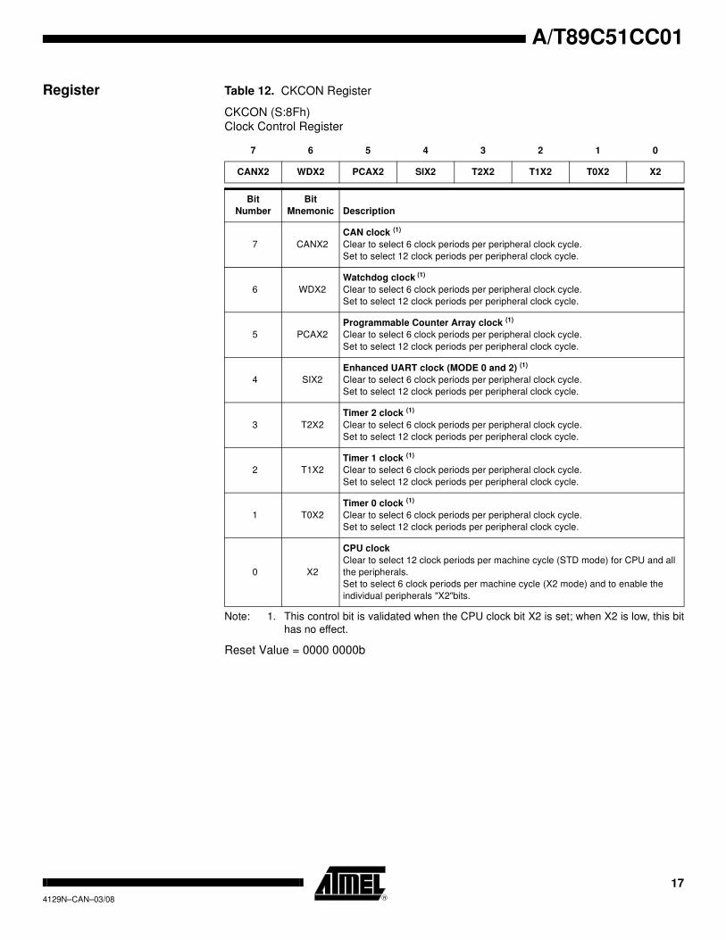
Register Table 12. CKCON Register
CKCON (S:8Fh)
Clock Control Register
Note: 1. This control bit is validated when the CPU clock bit X2 is set; when X2 is low, this bit
has no effect.
Reset Value = 0000 0000b
7 6 5 4 3 2 1 0
CANX2 WDX2 PCAX2 SIX2 T2X2 T1X2 T0X2 X2
Bit
Number
Bit
Mnemonic Description
7 CANX2
CAN clock (1)
Clear to select 6 clock periods per peripheral clock cycle.
Set to select 12 clock periods per peripheral clock cycle.
6 WDX2
Watchdog clock (1)
Clear to select 6 clock periods per peripheral clock cycle.
Set to select 12 clock periods per peripheral clock cycle.
5 PCAX2
Programmable Counter Array clock (1)
Clear to select 6 clock periods per peripheral clock cycle.
Set to select 12 clock periods per peripheral clock cycle.
4 SIX2
Enhanced UART clock (MODE 0 and 2) (1)
Clear to select 6 clock periods per peripheral clock cycle.
Set to select 12 clock periods per peripheral clock cycle.
3 T2X2
Timer 2 clock (1)
Clear to select 6 clock periods per peripheral clock cycle.
Set to select 12 clock periods per peripheral clock cycle.
2 T1X2
Timer 1 clock (1)
Clear to select 6 clock periods per peripheral clock cycle.
Set to select 12 clock periods per peripheral clock cycle.
1 T0X2
Timer 0 clock (1)
Clear to select 6 clock periods per peripheral clock cycle.
Set to select 12 clock periods per peripheral clock cycle.
0 X2
CPU clock
Clear to select 12 clock periods per machine cycle (STD mode) for CPU and all
the peripherals.
Set to select 6 clock periods per machine cycle (X2 mode) and to enable the
individual peripherals "X2"bits.

18 A/T89C51CC014129N–CAN–03/08
Power Management Two power reduction modes are implemented in the T89C51CC01: the Idle mode and
the Power-down mode. These modes are detailed in the following sections. In addition
to these power reduction modes, the clocks of the core and peripherals can be dynami-
cally divided by 2 using the X2 Mode detailed in Section “Clock”.
Reset Pin In order to start-up (cold reset) or to restart (warm reset) properly the microcontroller, a
high level has to be applied on the RST pin. A bad level leads to a wrong initialisation of
the internal registers like SFRs, PC, etc. and to unpredictable behavior of the microcon-
troller. A warm reset can be applied either directly on the RST pin or indirectly by an
internal reset source such as a watchdog, PCA, timer, etc.
At Power-up (Cold Reset) Two conditions are required before enabling a CPU start-up:
• VDD must reach the specified VDD range,
• The level on xtal1 input must be outside the specification (VIH, VIL).
If one of these two conditions are not met, the microcontroller does not start correctly
and can execute an instruction fetch from anywhere in the program space. An active
level applied on the RST pin must be maintained until both of the above conditions are
met. A reset is active when the level VIH1 is reached and when the pulse width covers
the period of time where VDD and the oscillator are not stabilized. Two parameters have
to be taken into account to determine the reset pulse width:
• VDD rise time (vddrst),
• Oscillator startup time (oscrst).
To determine the capacitor the highest value of these two parameters has to be chosen.
The reset circuitry is shown in Figure 7.
Figure 7. Reset Circuitry
Table 13 and Table 15 give some typical examples for three values of VDD rise times,
two values of oscillator start-up time and two pull-down resistor values.
Table 13. Minimum Reset Capacitor for a 15k Pull-down Resistor
Note: These values assume VDD starts from 0v to the nominal value. If the time between two
on/off sequences is too fast, the power-supply de coupling capacitors may not be fully
discharged, leading to a bad reset sequence.
oscrst/vddrst 1ms 10ms 100ms
5ms 2.7µF 4.7µF 47µF
20ms 10µF 15µF 47µF
0
VDD
Rrst
Crst
RST pin
Internal reset
Reset input circuitry

19
A/T89C51CC01
4129N–CAN–03/08
Warm Reset To achieve a valid reset, the reset signal must be maintained for at least 2 machine
cycles (24 oscillator clock periods) while the oscillator is running. The number of clock
periods is mode independent (X2 or X1).
Watchdog Reset As detailed in Section “PCA Watchdog Timer”, page 123, the WDT generates a 96-clock
period pulse on the RST pin. In order to properly propagate this pulse to the rest of the
application in case of external capacitor or power-supply supervisor circuit, a 1KΩ resis-
tor must be added as shown Figure 8.
Figure 8. Reset Circuitry for WDT reset out usage
Reset Recommendation to Prevent Flash Corruption
An example of bad initialization situation may occur in an instance where the bit
ENBOOT in AUXR1 register is initialized from the hardware bit BLJB upon reset. Since
this bit allows mapping of the bootloader in the code area, a reset failure can be critical.
If one wants the ENBOOT cleared in order to unmap the boot from the code area (yet
due to a bad reset) the bit ENBOOT in SFRs may be set. If the value of Program
Counter is accidently in the range of the boot memory addresses then a flash access
(write or erase) may corrupt the Flash on-chip memory.
It is recommended to use an external reset circuitry featuring power supply monitoring to
prevent system malfunction during periods of insufficient power supply voltage (power
supply failure, power supply switched off).
Idle Mode Idle mode is a power reduction mode that reduces the power consumption. In this mode,
program execution halts. Idle mode freezes the clock to the CPU at known states while
the peripherals continue to be clocked. The CPU status before entering Idle mode is
preserved, i.e., the program counter and program status word register retain their data
for the duration of Idle mode. The contents of the SFRs and RAM are also retained. The
status of the Port pins during Idle mode is detailed in Table 14.
Entering Idle Mode To enter Idle mode, you must set the IDL bit in PCON register (see Table 15). The
T89C51CC01 enters Idle mode upon execution of the instruction that sets IDL bit. The
instruction that sets IDL bit is the last instruction executed.
Note: If IDL bit and PD bit are set simultaneously, the T89C51CC01 enters Power-down mode.
Then it does not go in Idle mode when exiting Power-down mode.
Exiting Idle Mode There are two ways to exit Idle mode:
1. Generate an enabled interrupt.
– Hardware clears IDL bit in PCON register which restores the clock to the
CPU. Execution resumes with the interrupt service routine. Upon completion
RR
ST
RST
VSS
To CPU coreand peripherals
VDD
+
VSS
VDD
RST
1K
To otheron-boardcircuitry

20 A/T89C51CC014129N–CAN–03/08
of the interrupt service routine, program execution resumes with the
instruction immediately following the instruction that activated Idle mode.
The general-purpose flags (GF1 and GF0 in PCON register) may be used to
indicate whether an interrupt occurred during normal operation or during Idle
mode. When Idle mode is exited by an interrupt, the interrupt service routine
may examine GF1 and GF0.
2. Generate a reset.
– A logic high on the RST pin clears IDL bit in PCON register directly and
asynchronously. This restores the clock to the CPU. Program execution
momentarily resumes with the instruction immediately following the
instruction that activated the Idle mode and may continue for a number of
clock cycles before the internal reset algorithm takes control. Reset
initializes the T89C51CC01 and vectors the CPU to address C:0000h.
Note: 1. During the time that execution resumes, the internal RAM cannot be accessed; how-
ever, it is possible for the Port pins to be accessed. To avoid unexpected outputs at
the Port pins, the instruction immediately following the instruction that activated Idle
mode should not write to a Port pin or to the external RAM.
2. If Idle mode is invoked by ADC Idle, the ADC conversion completion will exit Idle.
Power-down Mode The Power-down mode places the T89C51CC01 in a very low power state. Power-down
mode stops the oscillator and freezes all clocks at known states. The CPU status prior to
entering Power-down mode is preserved, i.e., the program counter, program status
word register retain their data for the duration of Power-down mode. In addition, the
SFRs and RAM contents are preserved. The status of the Port pins during Power-down
mode is detailed in Table 14.
Entering Power-down Mode To enter Power-down mode, set PD bit in PCON register. The T89C51CC01 enters the
Power-down mode upon execution of the instruction that sets PD bit. The instruction
that sets PD bit is the last instruction executed.
Exiting Power-down Mode If VDD was reduced during the Power-down mode, do not exit Power-down mode until
VDD is restored to the normal operating level.
There are two ways to exit the Power-down mode:
1. Generate an enabled external interrupt.
– The T89C51CC01 provides capability to exit from Power-down using INT0#,
INT1#.
Hardware clears PD bit in PCON register which starts the oscillator and
restores the clocks to the CPU and peripherals. Using INTx# input,
execution resumes when the input is released (see Figure 9) while using
KINx input, execution resumes after counting 1024 clock ensuring the
oscillator is restarted properly (see Figure 8). Execution resumes with the
interrupt service routine. Upon completion of the interrupt service routine,
program execution resumes with the instruction immediately following the
instruction that activated Power-down mode.
Note: 1. The external interrupt used to exit Power-down mode must be configured as level
sensitive (INT0# and INT1#) and must be assigned the highest priority. In addition,
the duration of the interrupt must be long enough to allow the oscillator to stabilize.
The execution will only resume when the interrupt is deasserted.
2. Exit from power-down by external interrupt does not affect the SFRs nor the internal
RAM content.

21
A/T89C51CC01
4129N–CAN–03/08
Figure 9. Power-down Exit Waveform Using INT1:0#
2. Generate a reset.
– A logic high on the RST pin clears PD bit in PCON register directly and
asynchronously. This starts the oscillator and restores the clock to the CPU
and peripherals. Program execution momentarily resumes with the
instruction immediately following the instruction that activated Power-down
mode and may continue for a number of clock cycles before the internal
reset algorithm takes control. Reset initializes the T89C51CC01 and vectors
the CPU to address 0000h.
Notes: 1. During the time that execution resumes, the internal RAM cannot be accessed; how-
ever, it is possible for the Port pins to be accessed. To avoid unexpected outputs at
the Port pins, the instruction immediately following the instruction that activated the
Power-down mode should not write to a Port pin or to the external RAM.
2. Exit from power-down by reset redefines all the SFRs, but does not affect the internal
RAM content.
Table 14. Pin Conditions in Special Operating Modes
3.
INT1:0#
OSC
Power-down phase Oscillator restart phase Active phaseActive phase
Mode Port 0 Port 1 Port 2 Port 3 Port 4 ALE PSEN#
Reset Floating High High High High High High
Idle
(internal
code)
Data Data Data Data Data High High
Idle
(external
code)
Floating Data Data Data Data High High
Power-
Down(inter
nal code)
Data Data Data Data Data Low Low
Power-
Down
(external
code)
Floating Data Data Data Data Low Low
22 A/T89C51CC014129N–CAN–03/08
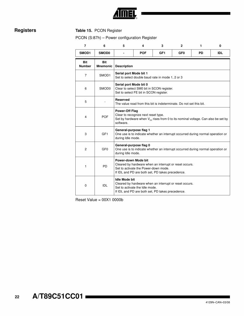
Registers Table 15. PCON Register
PCON (S:87h) – Power configuration Register
Reset Value = 00X1 0000b
7 6 5 4 3 2 1 0
SMOD1 SMOD0 - POF GF1 GF0 PD IDL
Bit
Number
Bit
Mnemonic Description
7 SMOD1Serial port Mode bit 1
Set to select double baud rate in mode 1, 2 or 3
6 SMOD0
Serial port Mode bit 0
Clear to select SM0 bit in SCON register.
Set to select FE bit in SCON register.
5 -Reserved
The value read from this bit is indeterminate. Do not set this bit.
4 POF
Power-Off Flag
Clear to recognize next reset type.
Set by hardware when Vcc rises from 0 to its nominal voltage. Can also be set by
software.
3 GF1
General-purpose flag 1
One use is to indicate whether an interrupt occurred during normal operation or
during Idle mode.
2 GF0
General-purpose flag 0
One use is to indicate whether an interrupt occurred during normal operation or
during Idle mode.
1 PD
Power-down Mode bit
Cleared by hardware when an interrupt or reset occurs.
Set to activate the Power-down mode.
If IDL and PD are both set, PD takes precedence.
0 IDL
Idle Mode bit
Cleared by hardware when an interrupt or reset occurs.
Set to activate the Idle mode.
If IDL and PD are both set, PD takes precedence.

23
A/T89C51CC01
4129N–CAN–03/08
Data Memory The T89C51CC01 provides data memory access in two different spaces:
1. The internal space mapped in three separate segments:
• the lower 128 Bytes RAM segment.
• the upper 128 Bytes RAM segment.
• the expanded 1024 Bytes RAM segment (XRAM).
2. The external space.
A fourth internal segment is available but dedicated to Special Function Registers,
SFRs, (addresses 80h to FFh) accessible by direct addressing mode.
Figure 11 shows the internal and external data memory spaces organization.
Figure 10. Internal Memory - RAM
Figure 11. Internal and External Data Memory Organization XRAM-XRAM
Upper128 Bytes
Internal RAM
Lower128 Bytes
Internal RAM
SpecialFunctionRegisters
80h 80h
00h
FFh FFh
direct addressing
addressing
7Fh
direct or indirect
indirect addressing
256 up to 1024 Bytes
00h
64K BytesExternal XRAM
0000h
FFFFh
Internal XRAMEXTRAM = 0
EXTRAM = 1
FFh or 3FFh
Internal External

24 A/T89C51CC014129N–CAN–03/08
Internal Space
Lower 128 Bytes RAM The lower 128 Bytes of RAM (see Figure 11) are accessible from address 00h to 7Fh
using direct or indirect addressing modes. The lowest 32 Bytes are grouped into 4
banks of 8 registers (R0 to R7). Two bits RS0 and RS1 in PSW register (see Figure 18)
select which bank is in use according to Table 16. This allows more efficient use of code
space, since register instructions are shorter than instructions that use direct address-
ing, and can be used for context switching in interrupt service routines.
Table 16. Register Bank Selection
The next 16 Bytes above the register banks form a block of bit-addressable memory
space. The C51 instruction set includes a wide selection of single-bit instructions, and
the 128 bits in this area can be directly addressed by these instructions. The bit
addresses in this area are 00h to 7Fh.
Figure 12. Lower 128 Bytes Internal RAM Organization
Upper 128 Bytes RAM The upper 128 Bytes of RAM are accessible from address 80h to FFh using only indirect
addressing mode.
Expanded RAM The on-chip 1024 Bytes of expanded RAM (XRAM) are accessible from address 0000h
to 03FFh using indirect addressing mode through MOVX instructions. In this address
range, the bit EXTRAM in AUXR register is used to select the XRAM (default) or the
XRAM. As shown in Figure 11 when EXTRAM = 0, the XRAM is selected and when
EXTRAM = 1, the XRAM is selected.
The size of XRAM can be configured by XRS1-0 bit in AUXR register (default size is
1024 Bytes).
Note: Lower 128 Bytes RAM, Upper 128 Bytes RAM, and expanded RAM are made of volatile
memory cells. This means that the RAM content is indeterminate after power-up and
must then be initialized properly.
RS1 RS0 Description
0 0 Register bank 0 from 00h to 07h
0 1 Register bank 0 from 08h to 0Fh
1 0 Register bank 0 from 10h to 17h
1 1 Register bank 0 from 18h to 1Fh
Bit-Addressable Space
4 Banks of 8 RegistersR0-R7
30h
7Fh
(Bit Addresses 0-7Fh)20h
2Fh
18h1Fh
10h17h
08h0Fh
00h07h

25
A/T89C51CC01
4129N–CAN–03/08
External Space
Memory Interface The external memory interface comprises the external bus (port 0 and port 2) as well as
the bus control signals (RD, WR, and ALE).
Figure 13 shows the structure of the external address bus. P0 carries address A7:0
while P2 carries address A15:8. Data D7:0 is multiplexed with A7:0 on P0. Table 17
describes the external memory interface signals.
Figure 13. External Data Memory Interface Structure
Table 17. External Data Memory Interface Signals
External Bus Cycles This section describes the bus cycles the T89C51CC01 executes to read (see
Figure 14), and write data (see Figure 15) in the external data memory.
External memory cycle takes 6 CPU clock periods. This is equivalent to 12 oscillator
clock period in standard mode or 6 oscillator clock periods in X2 mode. For further infor-
mation on X2 mode.
Slow peripherals can be accessed by stretching the read and write cycles. This is done
using the M0 bit in AUXR register. Setting this bit changes the width of the RD and WR
signals from 3 to 15 CPU clock periods.
For simplicity, the accompanying figures depict the bus cycle waveforms in idealized
form and do not provide precise timing information. For bus cycle timing parameters
refer to the Section “AC Characteristics”.
Signal
Name Type Description
Alternative
Function
A15:8 OAddress Lines
Upper address lines for the external bus.P2.7:0
AD7:0 I/O
Address/Data Lines
Multiplexed lower address lines and data for the external
memory.
P0.7:0
ALE O
Address Latch Enable
ALE signals indicates that valid address information are available
on lines AD7:0.
-
RD ORead
Read signal output to external data memory.P3.7
WR OWrite
Write signal output to external memory.P3.6
RAM
PERIPHERALT89C51CC01
P2
P0AD7:0
A15:8
A7:0
A15:8
D7:0
A7:0
ALE
WR
OERD
WR
Latch

26 A/T89C51CC014129N–CAN–03/08
Figure 14. External Data Read Waveforms
Notes: 1. RD signal may be stretched using M0 bit in AUXR register.
2. When executing MOVX @Ri instruction, P2 outputs SFR content.
Figure 15. External Data Write Waveforms
Notes: 1. WR signal may be stretched using M0 bit in AUXR register.
2. When executing MOVX @Ri instruction, P2 outputs SFR content.
ALE
P0
P2
RD 1
DPL or Ri D7:0
DPH or P22P2
CPU Clock
ALE
P0
P2
WR1
DPL or Ri D7:0
P2
CPU Clock
DPH or P22
27
A/T89C51CC01
4129N–CAN–03/08
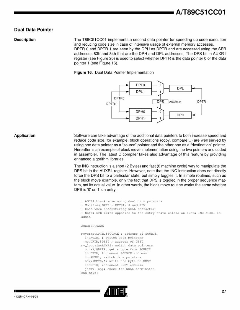
Dual Data Pointer
Description The T89C51CC01 implements a second data pointer for speeding up code execution
and reducing code size in case of intensive usage of external memory accesses.
DPTR 0 and DPTR 1 are seen by the CPU as DPTR and are accessed using the SFR
addresses 83h and 84h that are the DPH and DPL addresses. The DPS bit in AUXR1
register (see Figure 20) is used to select whether DPTR is the data pointer 0 or the data
pointer 1 (see Figure 16).
Figure 16. Dual Data Pointer Implementation
Application Software can take advantage of the additional data pointers to both increase speed and
reduce code size, for example, block operations (copy, compare…) are well served by
using one data pointer as a “source” pointer and the other one as a “destination” pointer.
Hereafter is an example of block move implementation using the two pointers and coded
in assembler. The latest C compiler takes also advantage of this feature by providing
enhanced algorithm libraries.
The INC instruction is a short (2 Bytes) and fast (6 machine cycle) way to manipulate the
DPS bit in the AUXR1 register. However, note that the INC instruction does not directly
force the DPS bit to a particular state, but simply toggles it. In simple routines, such as
the block move example, only the fact that DPS is toggled in the proper sequence mat-
ters, not its actual value. In other words, the block move routine works the same whether
DPS is '0' or '1' on entry.
; ASCII block move using dual data pointers
; Modifies DPTR0, DPTR1, A and PSW
; Ends when encountering NULL character
; Note: DPS exits opposite to the entry state unless an extra INC AUXR1 is
added
AUXR1EQU0A2h
move:movDPTR,#SOURCE ; address of SOURCE
incAUXR1 ; switch data pointers
movDPTR,#DEST ; address of DEST
mv_loop:incAUXR1; switch data pointers
movxA,@DPTR; get a byte from SOURCE
incDPTR; increment SOURCE address
incAUXR1; switch data pointers
movx@DPTR,A; write the byte to DEST
incDPTR; increment DEST address
jnzmv_loop; check for NULL terminator
end_move:
0
1
DPH0
DPH1
DPL0
0
1
DPS AUXR1.0
DPH
DPLDPL1
DPTRDPTR0
DPTR1

28 A/T89C51CC014129N–CAN–03/08
Registers Table 18. PSW Register
PSW (S:D0h)
Program Status Word Register
Reset Value = 0000 0000b
Table 19. AUXR Register
AUXR (S:8Eh)
Auxiliary Register
7 6 5 4 3 2 1 0
CY AC F0 RS1 RS0 OV F1 P
Bit
Number
Bit
Mnemonic Description
7 CYCarry Flag
Carry out from bit 1 of ALU operands.
6 ACAuxiliary Carry Flag
Carry out from bit 1 of addition operands.
5 F0 User Definable Flag 0.
4-3 RS1:0Register Bank Select Bits
Refer to Table 16 for bits description.
2 OVOverflow Flag
Overflow set by arithmetic operations.
1 F1 User Definable Flag 1
0 P
Parity Bit
Set when ACC contains an odd number of 1’s.
Cleared when ACC contains an even number of 1’s.
7 6 5 4 3 2 1 0
- - M0 - XRS1 XRS0 EXTRAM A0
Bit
Number
Bit
Mnemonic Description
7-6 -Reserved
The value read from these bits are indeterminate. Do not set this bit.
5 M0
Stretch MOVX control:
the RD/ and the WR/ pulse length is increased according to the value of M0.
M0 Pulse length in clock period
0 6
1 30
4 -Reserved
The value read from this bit is indeterminate. Do not set this bit.
3-2 XRS1-0
XRAM size:
Accessible size of the XRAM
XRS 1:0 XRAM size
0 0 256 Bytes
0 1 512 Bytes
1 0 768 Bytes
1 1 1024 Bytes (default)

29
A/T89C51CC01
4129N–CAN–03/08
Reset Value = X00X 1100b
Not bit addressable
Table 20. AUXR1 Register
AUXR1 (S:A2h)
Auxiliary Control Register 1
Reset Value = XXXX 00X0b
Note: 1. ENBOOT is initialized with the invert BLJB at reset. See In-System Programming
section.
1 EXTRAM
Internal/External RAM (00h - FFh)
access using MOVX @ Ri/@ DPTR
0 - Internal XRAM access using MOVX @ Ri/@ DPTR.
1 - External data memory access.
0 A0
Disable/Enable ALE)
0 - ALE is emitted at a constant rate of 1/6 the oscillator frequency (or 1/3 if X2
mode is used)
1 - ALE is active only during a MOVX or MOVC instruction.
7 6 5 4 3 2 1 0
- - ENBOOT - GF3 0 - DPS
Bit
Number
Bit
Mnemonic Description
7-6 -Reserved
The value read from these bits is indeterminate. Do not set these bits.
5 ENBOOT(1)
Enable Boot Flash
Set this bit for map the boot Flash between F800h -FFFFh
Clear this bit for disable boot Flash.
4 -Reserved
The value read from this bit is indeterminate. Do not set this bit.
3 GF3 General-purpose Flag 3
2 0
Always Zero
This bit is stuck to logic 0 to allow INC AUXR1 instruction without affecting GF3
flag.
1 - Reserved for Data Pointer Extension.
0 DPS
Data Pointer Select Bit
Set to select second dual data pointer: DPTR1.
Clear to select first dual data pointer: DPTR0.
Bit
Number
Bit
Mnemonic Description
30 A/T89C51CC014129N–CAN–03/08
EEPROM Data
Memory
The 2-Kbyte on-chip EEPROM memory block is located at addresses 0000h to 07FFh of
the XRAM/XRAM memory space and is selected by setting control bits in the EECON
register. A read in the EEPROM memory is done with a MOVX instruction.
A physical write in the EEPROM memory is done in two steps: write data in the column
latches and transfer of all data latches into an EEPROM memory row (programming).
The number of data written on the page may vary from 1 up to 128 Bytes (the page
size). When programming, only the data written in the column latch is programmed and
a ninth bit is used to obtain this feature. This provides the capability to program the
whole memory by Bytes, by page or by a number of Bytes in a page. Indeed, each ninth
bit is set when the writing the corresponding byte in a row and all these ninth bits are
reset after the writing of the complete EEPROM row.
Write Data in the Column Latches
Data is written by byte to the column latches as for an external RAM memory. Out of the
11 address bits of the data pointer, the 4 MSBs are used for page selection (row) and 7
are used for byte selection. Between two EEPROM programming sessions, all the
addresses in the column latches must stay on the same page, meaning that the 4 MSB
must no be changed.
The following procedure is used to write to the column latches:
• Save and disable interrupt.
• Set bit EEE of EECON register
• Load DPTR with the address to write
• Store A register with the data to be written
• Execute a MOVX @DPTR, A
• If needed loop the three last instructions until the end of a 128 Bytes page
• Restore interrupt.
Note: The last page address used when loading the column latch is the one used to select the
page programming address.
Programming The EEPROM programming consists of the following actions:
• writing one or more Bytes of one page in the column latches. Normally, all Bytes
must belong to the same page; if not, the last page address will be latched and the
others discarded.
• launching programming by writing the control sequence (50h followed by A0h) to the
EECON register.
• EEBUSY flag in EECON is then set by hardware to indicate that programming is in
progress and that the EEPROM segment is not available for reading.
• The end of programming is indicated by a hardware clear of the EEBUSY flag.
Note: The sequence 5xh and Axh must be executed without instructions between then other-
wise the programming is aborted.
Read Data The following procedure is used to read the data stored in the EEPROM memory:
• Save and disable interrupt
• Set bit EEE of EECON register
• Load DPTR with the address to read
• Execute a MOVX A, @DPTR
• Restore interrupt

31
A/T89C51CC01
4129N–CAN–03/08
Examples ;*F*************************************************************************
;* NAME: api_rd_eeprom_byte
;* DPTR contain address to read.
;* Acc contain the reading value
;* NOTE: before execute this function, be sure the EEPROM is not BUSY
;***************************************************************************
api_rd_eeprom_byte:
; Save and clear EA
MOV EECON, #02h; map EEPROM in XRAM space
MOVX A, @DPTR
MOV EECON, #00h; unmap EEPROM
; Restore EA
ret
;*F*************************************************************************
;* NAME: api_ld_eeprom_cl
;* DPTR contain address to load
;* Acc contain value to load
;* NOTE: in this example we load only 1 byte, but it is possible upto
;* 128 Bytes.
;* before execute this function, be sure the EEPROM is not BUSY
;***************************************************************************
api_ld_eeprom_cl:
; Save and clear EA
MOV EECON, #02h ; map EEPROM in XRAM space
MOVX @DPTR, A
MOVEECON, #00h; unmap EEPROM
; Restore EA
ret
;*F*************************************************************************
;* NAME: api_wr_eeprom
;* NOTE: before execute this function, be sure the EEPROM is not BUSY
;***************************************************************************
api_wr_eeprom:
; Save and clear EA
MOV EECON, #050h
MOV EECON, #0A0h
; Restore EA
ret

32 A/T89C51CC014129N–CAN–03/08
Registers Table 21. EECON Register
EECON (S:0D2h)
EEPROM Control Register
Reset Value = XXXX XX00b
Not bit addressable
7 6 5 4 3 2 1 0
EEPL3 EEPL2 EEPL1 EEPL0 - - EEE EEBUSY
Bit Number
Bit
Mnemonic Description
7-4 EEPL3-0Programming Launch command bits
Write 5Xh followed by AXh to EEPL to launch the programming.
3 -Reserved
The value read from this bit is indeterminate. Do not set this bit.
2 -Reserved
The value read from this bit is indeterminate. Do not set this bit.
1 EEE
Enable EEPROM Space bit
Set to map the EEPROM space during MOVX instructions (Write in the column
latches)
Clear to map the XRAM space during MOVX.
0 EEBUSY
Programming Busy flag
Set by hardware when programming is in progress.
Cleared by hardware when programming is done.
Can not be set or cleared by software.

33
A/T89C51CC01
4129N–CAN–03/08
Program/Code
Memory
The T89C51CC01 implement 32K Bytes of on-chip program/code memory. Figure 17
shows the partitioning of internal and external program/code memory spaces depending
on the product.
The Flash memory increases EPROM and ROM functionality by in-circuit electrical era-
sure and programming. Thanks to the internal charge pump, the high voltage needed for
programming or erasing Flash cells is generated on-chip using the standard VDD volt-
age. Thus, the Flash Memory can be programmed using only one voltage and allows In-
System-Programming commonly known as ISP. Hardware programming mode is also
available using specific programming tool.
Figure 17. Program/Code Memory Organization
Notes: 1. If the program executes exclusively from on-chip code memory (not from external
memory), beware of executing code from the upper byte of on-chip memory (7FFFh)
and thereby disrupt I/O Ports 0 and 2 due to external prefetch. Fetching code con-
stant from this location does not affect Ports 0 and 2.
2. Default factory programmed parts come with maximum hardware protection. Execu-
tion from external memory is not possible unless the Hardware Security Byte is
reprogrammed. See Table 27.
0000h
32K Bytes
7FFFh
internal
0000h
7FFFh
FFFFh
8000h
Flash
32K Bytesexternalmemory
32K Bytesexternalmemory
EA = 0EA = 1

34 A/T89C51CC014129N–CAN–03/08
17.22 External Code Memory Access
Memory Interface The external memory interface comprises the external bus (port 0 and port 2) as well as
the bus control signals (PSEN#, and ALE).
Figure 18 shows the structure of the external address bus. P0 carries address A7:0
while P2 carries address A15:8. Data D7:0 is multiplexed with A7:0 on P0. Table 18
describes the external memory interface signals.
Figure 18. External Code Memory Interface Structure
External Bus Cycles This section describes the bus cycles the T89C51CC01 executes to fetch code (see
Figure 19) in the external program/code memory.
External memory cycle takes 6 CPU clock periods. This is equivalent to 12 oscillator
clock period in standard mode or 6 oscillator clock periods in X2 mode. For further infor-
mation on X2 mode see section “Clock “.
For simplicity, the accompanying figure depicts the bus cycle waveforms in idealized
form and do not provide precise timing information.
For bus cycling parameters refer to the ‘AC-DC parameters’ section.
Table 23. External Code Memory Interface Signals
Signal
Name Type Description
Alternate
Function
A15:8 OAddress Lines
Upper address lines for the external bus.P2.7:0
AD7:0 I/OAddress/Data Lines
Multiplexed lower address lines and data for the external memory.P0.7:0
ALE O
Address Latch Enable
ALE signals indicates that valid address information are available on lines
AD7:0.
-
PSEN# O
Program Store Enable Output
This signal is active low during external code fetch or external code read
(MOVC instruction).
-
Flash
EPROMT89C51CC01
P2
P0AD7:0
A15:8
A7:0
A15:8
D7:0
A7:0
ALELatch
OEPSEN#

35
A/T89C51CC01
4129N–CAN–03/08
Figure 19. External Code Fetch Waveforms
Flash Memory Architecture
T89C51CC01 features two on-chip Flash memories:
• Flash memory FM0:
containing 32K Bytes of program memory (user space) organized into 128 byte
pages,
• Flash memory FM1:
2K Bytes for boot loader and Application Programming Interfaces (API).
The FM0 can be program by both parallel programming and Serial In-System-Program-
ming (ISP) whereas FM1 supports only parallel programming by programmers. The ISP
mode is detailed in the "In-System-Programming" section.
All Read/Write access operations on Flash Memory by user application are managed by
a set of API described in the "In-System-Programming" section.
Figure 20. Flash Memory Architecture
ALE
P0
P2
PSEN#
PCL
PCHPCH
PCLD7:0 D7:0
PCH
D7:0
CPU Clock
7FFFh
32K Bytes
Flash memory
FM0
0000h
Hardware Security (1 byte)
Column Latches (128 Bytes)
user space
Extra Row (128 Bytes)
2K Bytes
Flash memory
FM1
boot space
FFFFh
F800h
FM1 mapped between F800h andFFFFh when bit ENBOOT is set in AUXR1 register

36 A/T89C51CC014129N–CAN–03/08
FM0 Memory Architecture The Flash memory is made up of 4 blocks (see Figure 20):
• The memory array (user space) 32K Bytes
• The Extra Row
• The Hardware security bits
• The column latch registers
User Space This space is composed of a 32K Bytes Flash memory organized in 256 pages of 128
Bytes. It contains the user’s application code.
Extra Row (XRow) This row is a part of FM0 and has a size of 128 Bytes. The extra row may contain infor-
mation for boot loader usage.
Hardware Security Byte The Hardware security Byte space is a part of FM0 and has a size of 1 byte.
The 4 MSB can be read/written by software, the 4 LSB can only be read by software and
written by hardware in parallel mode.
Column Latches The column latches, also part of FM0, have a size of full page (128 Bytes).
The column latches are the entrance buffers of the three previous memory locations
(user array, XROW and Hardware security byte).
Cross Flash Memory Access
Description
The FM0 memory can be program only from FM1. Programming FM0 from FM0 or from
external memory is impossible.
The FM1 memory can be program only by parallel programming.
The Table 24 show all software Flash access allowed.
Table 24. Cross Flash Memory Access
Co
de
ex
ec
uti
ng
fro
m
Action
FM0
(user Flash)
FM1
(boot Flash)
FM0
(user Flash)
Read ok -
Load column latch ok -
Write - -
FM1
(boot Flash)
Read ok ok
Load column latch ok -
Write ok -
External
memory
EA = 0
Read - -
Load column latch - -
Write - -

37
A/T89C51CC01
4129N–CAN–03/08
Overview of FM0 Operations
The CPU interfaces to the Flash memory through the FCON register and AUXR1
register.
These registers are used to:
• Map the memory spaces in the adressable space
• Launch the programming of the memory spaces
• Get the status of the Flash memory (busy/not busy)
Mapping of the Memory Space By default, the user space is accessed by MOVC instruction for read only. The column
latches space is made accessible by setting the FPS bit in FCON register. Writing is
possible from 0000h to 7FFFh, address bits 6 to 0 are used to select an address within a
page while bits 14 to 7 are used to select the programming address of the page.
Setting FPS bit takes precedence on the EXTRAM bit in AUXR register.
The other memory spaces (user, extra row, hardware security) are made accessible in
the code segment by programming bits FMOD0 and FMOD1 in FCON register in accor-
dance with Table 25. A MOVC instruction is then used for reading these spaces.
Table 25. FM0 Blocks Select Bits
Launching Programming FPL3:0 bits in FCON register are used to secure the launch of programming. A specific
sequence must be written in these bits to unlock the write protection and to launch the
programming. This sequence is 5xh followed by Axh. Table 26 summarizes the memory
spaces to program according to FMOD1:0 bits.
FMOD1 FMOD0 FM0 Adressable space
0 0 User (0000h-7FFFh)
0 1 Extra Row(FF80h-FFFFh)
1 0 Hardware Security Byte (0000h)
1 1 Reserved

38 A/T89C51CC014129N–CAN–03/08
Table 26. Programming Spaces
Notes: 1. The sequence 5xh and Axh must be executing without instructions between them
otherwise the programming is aborted.
2. Interrupts that may occur during programming time must be disabled to avoid any
spurious exit of the programming mode.
Status of the Flash Memory The bit FBUSY in FCON register is used to indicate the status of programming.
FBUSY is set when programming is in progress.
Selecting FM1 The bit ENBOOT in AUXR1 register is used to map FM1 from F800h to FFFFh.
Loading the Column Latches Any number of data from 1 Byte to 128 Bytes can be loaded in the column latches. This
provides the capability to program the whole memory by byte, by page or by any number
of Bytes in a page.
When programming is launched, an automatic erase of the locations loaded in the col-
umn latches is first performed, then programming is effectively done. Thus no page or
block erase is needed and only the loaded data are programmed in the corresponding
page.
The following procedure is used to load the column latches and is summarized in
Figure 21:
• Save then disable interrupt and map the column latch space by setting FPS bit.
• Load the DPTR with the address to load.
• Load Accumulator register with the data to load.
• Execute the MOVX @DPTR, A instruction.
• If needed loop the three last instructions until the page is completely loaded.
• Unmap the column latch and Restore Interrupt
Write to FCON
OperationFPL3:0 FPS FMOD1 FMOD0
User
5 X 0 0 No action
A X 0 0Write the column latches in user
space
Extra Row
5 X 0 1 No action
A X 0 1Write the column latches in extra row
space
Hardware
Security
Byte
5 X 1 0 No action
A X 1 0 Write the fuse bits space
Reserved
5 X 1 1 No action
A X 1 1 No action

39
A/T89C51CC01
4129N–CAN–03/08
Figure 21. Column Latches Loading Procedure
Note: The last page address used when loading the column latch is the one used to select the
page programming address.
Programming the Flash Spaces
User The following procedure is used to program the User space and is summarized in
Figure 22:
• Load up to one page of data in the column latches from address 0000h to 7FFFh.
• Save then disable the interrupts.
• Launch the programming by writing the data sequence 50h followed by A0h in
FCON register (only from FM1).
The end of the programming indicated by the FBUSY flag cleared.
• Restore the interrupts.
Extra Row The following procedure is used to program the Extra Row space and is summarized in
Figure 22:
• Load data in the column latches from address FF80h to FFFFh.
• Save then disable the interrupts.
• Launch the programming by writing the data sequence 52h followed by A2h in
FCON register. This step of the procedure must be executed from FM1. The end of
the programming indicated by the FBUSY flag cleared.
The end of the programming indicated by the FBUSY flag cleared.
• Restore the interrupts.
Column Latches
Loading
Data LoadDPTR = Address
ACC = DataExec: MOVX @DPTR, A
Last Byte
to load?
Column Latches MappingFCON = 08h (FPS=1)
Data memory MappingFCON = 00h (FPS = 0)
Save and Disable ITEA = 0
Restore IT

40 A/T89C51CC014129N–CAN–03/08
Figure 22. Flash and Extra Row Programming Procedure
Hardware Security Byte The following procedure is used to program the Hardware Security Byte spaceand is summarized in Figure 23:
• Set FPS and map Hardware byte (FCON = 0x0C)
• Save and disable the interrupts.
• Load DPTR at address 0000h.
• Load Accumulator register with the data to load.
• Execute the MOVX @DPTR, A instruction.
• Launch the programming by writing the data sequence 54h followed by A4h in
FCON register. This step of the procedure must be executed from FM1. The end of
the programming indicated by the FBUSY flag cleared.
The end of the programming indicated by the FBusy flag cleared.
• Restore the interrupts.
Flash Spaces
Programming
Save and Disable ITEA = 0
Launch ProgrammingFCON = 5xhFCON = Axh
End ProgrammingRestore IT
Column Latches Loadingsee Figure 21
FBusy
Cleared?
Clear ModeFCON = 00h

41
A/T89C51CC01
4129N–CAN–03/08
Figure 23. Hardware Programming Procedure
Reading the Flash Spaces
User The following procedure is used to read the User space:
• Read one byte in Accumulator by executing MOVC A,@A+DPTR where A+DPTR is
the address of the code byte to read.
Note: FCON is supposed to be reset when not needed.
Extra Row The following procedure is used to read the Extra Row space and is summarized in
Figure 24:
• Map the Extra Row space by writing 02h in FCON register.
• Read one byte in Accumulator by executing MOVC A,@A+DPTR with A = 0 and
DPTR = FF80h to FFFFh.
• Clear FCON to unmap the Extra Row.
Hardware Security Byte The following procedure is used to read the Hardware Security space and issummarized in Figure 24:
• Map the Hardware Security space by writing 04h in FCON register.
• Read the byte in Accumulator by executing MOVC A,@A+DPTR with A = 0 and
DPTR = 0000h.
• Clear FCON to unmap the Hardware Security Byte.
Flash Spaces
Programming
Save and Disable ITEA = 0
Launch ProgrammingFCON = 54hFCON = A4h
End ProgrammingRestoreIT
FBusy
Cleared?
Clear ModeFCON = 00h
Data LoadDPTR = 00hACC = Data
Exec: MOVX @DPTR, A
FCON = 0Ch
Save and Disable ITEA = 0
End LoadingRestore IT
42 A/T89C51CC014129N–CAN–03/08
Figure 24. Reading Procedure
Note: 1. aa = 10 for the Hardware Security Byte.
Flash Protection from Parallel
Programming
The three lock bits in Hardware Security Byte (see "In-System-Programming" section)
are programmed according to Table 27 provide different level of protection for the on-
chip code and data located in FM0 and FM1.
The only way to write these bits are the parallel mode. They are set by default to level 4
Table 27. Program Lock bit
Program Lock bits
U: unprogrammed
P: programmed
WARNING: Security level 2 and 3 should only be programmed after Flash and Core
verification.
Preventing Flash Corruption See the “Power Management” section.
Flash Spaces Reading
Flash Spaces MappingFCON = 0000aa0b(1)
Data ReadDPTR = Address
ACC = 0Exec: MOVC A, @A+DPTR
Clear ModeFCON = 00h
Program Lock Bits
Protection Description
Security
LevelLB0 LB1 LB2
1 U U UNo program lock features enabled. MOVC instruction executed from
external program memory returns non coded data.
2 P U U
MOVC instructions executed from external program memory are barred
to return code bytes from internal memory, EA is sampled and latched
on reset, and further parallel programming of the Flash is disabled.
3 U P USame as 2, also verify through parallel programming interface is
disabled.
4 U U PSame as 3, also external execution is disabled if code roll over beyond
7FFFh

43
A/T89C51CC01
4129N–CAN–03/08
Registers FCON RegisterFCON (S:D1h)
Flash Control Register
Reset Value = 0000 0000b
7 6 5 4 3 2 1 0
FPL3 FPL2 FPL1 FPL0 FPS FMOD1 FMOD0 FBUSY
Bit
Number
Bit
Mnemonic Description
7-4 FPL3:0
Programming Launch Command Bits
Write 5Xh followed by AXh to launch the programming according to FMOD1:0
(see Table 26)
3 FPS
Flash Map Program Space
Set to map the column latch space in the data memory space.
Clear to re-map the data memory space.
2-1 FMOD1:0Flash Mode
See Table 25 or Table 26.
0 FBUSY
Flash Busy
Set by hardware when programming is in progress.
Clear by hardware when programming is done.
Can not be changed by software.
44 A/T89C51CC014129N–CAN–03/08
Operation Cross
Memory Access
Space addressable in read and write are:
• RAM
• ERAM (Expanded RAM access by movx)
• XRAM (eXternal RAM)
• EEPROM DATA
• FM0 (user flash)
• Hardware byte
• XROW
• Boot Flash
• Flash Column latch
The table below provide the different kind of memory which can be accessed from differ-
ent code location.
Note: 1. RWW: Read While Write
Table 28. Cross Memory Access
Action RAM
XRAM
ERAM Boot FLASH FM0 E² Data
Hardware
Byte XROW
boot FLASHRead OK OK OK OK -
Write - OK(1) OK(1) OK(1) OK(1)
FM0Read - OK OK OK -
Write - OK (idle) OK(1) - OK
External
memory
EA = 0
or Code Roll
Over
Read - - OK - -
Write - - OK(1) - -

45
A/T89C51CC01
4129N–CAN–03/08
Sharing Instructions Table 29. Instructions shared
Note: by cl: using Column Latch
Table 30. Read MOVX A, @DPTR
Table 31. Write MOVX @DPTR,A
Action RAM
XRAM
ERAM
EEPROM
DATA
Boot
FLASH FM0
Hardware
Byte XROW
Read MOV MOVX MOVX MOVC MOVC MOVC MOVC
Write MOV MOVX MOVX - by cl by cl by cl
EEE bit in
EECON
Register
FPS in
FCON Register ENBOOT EA
XRAM
ERAM
EEPROM
DATA
Flash
Column
Latch
0 0 X X OK
0 1 X X OK
1 0 X X OK
1 1 X X OK
EEE bit in
EECON
Register
FPS bit in
FCON Register ENBOOT EA
XRAM
ERAM
EEPROM
Data
Flash
Column
Latch
0 0 X X OK
0 1 X1 OK
0 OK
1 0 X X OK
1 1 X1 OK
0 OK

46 A/T89C51CC014129N–CAN–03/08
Table 32. Read MOVC A, @DPTR
Code Execution
FCON Register
ENBOOT DPTR FM1 FM0 XROW
Hardware
Byte
External
CodeFMOD1 FMOD0 FPS
From FM0
0 0 X
0 0000h to 7FFFh OK
10000h to 7FFFh OK
F800h to FFFFh Do not use this configuration
0 1 X X0000 to 007Fh
See (1)OK
1 0 X X X OK
1 1 X
0 000h to 7FFFh OK
10000h to 7FFFh OK
F800h to FFFFh Do not use this configuration
From FM1
(ENBOOT =1
0 0
01
0000h to 7FFF OK
F800h to FFFFh OK
0 X NA
11 X OK
0 X NA
0 1 X1 0000h to 007h
See (2)
OK
0 NA
1 0 X1
XOK
0 NA
1 1 X1
000h to 7FFFhOK
0 NA
External code:
EA=0 or Code
Roll Over
X 0 X X X OK
1. For DPTR higher than 007Fh only lowest 7 bits are decoded, thus the behavior is the same as for addresses from 0000h to
007Fh
2. For DPTR higher than 007Fh only lowest 7 bits are decoded, thus the behavior is the same as for addresses from 0000h to
007Fh

47
A/T89C51CC01
4129N–CAN–03/08
In-System
Programming (ISP)
With the implementation of the User Space (FM0) and the Boot Space (FM1) in Flash
technology the T89C51CC01 allows the system engineer the development of applica-
tions with a very high level of flexibility. This flexibility is based on the possibility to alter
the customer program at any stages of a product’s life:
• Before mounting the chip on the PCB, FM0 Flash can be programmed with the
application code. FM1 is always pre programmed by Atmel with a bootloader (chip
can be ordered with CAN bootloader or UART bootloader).(1)
• Once the chip is mounted on the PCB, it can be programmed by serial mode via the
CAN bus or UART.
Note: 1. The user can also program his own bootloader in FM1.
This In-System-Programming (ISP) allows code modification over the total lifetime of the
product.
Besides the default Boot loader Atmel provide to the customer also all the needed Appli-
cation-Programming-Interfaces (API) which are needed for the ISP. The API are located
also in the Boot memory.
This allow the customer to have a full use of the 32-Kbyte user memory.
Flash Programming and Erasure
There are three methods of programming the Flash memory:
• The Atmel bootloader located in FM1 is activated by the application. Low level API
routines (located in FM1)will be used to program FM0. The interface used for serial
downloading to FM0 is the UART or the CAN. API can be called also by the user’s
bootloader located in FM0 at [SBV]00h.
• A further method exists in activating the Atmel boot loader by hardware activation.
See Section “Hardware Security Byte”.
• The FM0 can be programmed also by the parallel mode using a programmer.
Figure 25. Flash Memory Mapping
F800h
7FFFh
32K Bytes
Flash memory
2K Bytes IAPbootloader
FM0
FM1
CustomBoot Loader
[SBV]00h
FFFFh
FM1 mapped between F800h and FFFFhwhen API called
0000h

48 A/T89C51CC014129N–CAN–03/08
Boot Process
Software Boot Process
Example
Many algorithms can be used for the software boot process. Below are descriptions of
the different flags and Bytes.
Boot Loader Jump Bit (BLJB):
- This bit indicates if on RESET the user wants to jump to this application at address
@0000h on FM0 or execute the boot loader at address @F800h on FM1.
- BLJB = 0 (i.e. bootloader FM1 executed after a reset) is the default Atmel factory pro-
gramming.
- To read or modify this bit, the APIs are used.
Boot Vector Address (SBV):
- This byte contains the MSB of the user boot loader address in FM0.
- The default value of SBV is FCh (no user boot loader in FM0).
- To read or modify this byte, the APIs are used.
Extra Byte (EB) and Boot Status Byte (BSB):
- These Bytes are reserved for customer use.
- To read or modify these Bytes, the APIs are used.
Hardware Boot Process At the falling edge of RESET, the bit ENBOOT in AUXR1 register is initialized with the
value of Boot Loader Jump Bit (BLJB).
Further at the falling edge of RESET if the following conditions (called Hardware condi-
tion) are detected. The FCON register is initialized with the value 00h and the PC is
initialized with F800h (FM1 lower byte = Bootloader entry point).
Hardware Conditions:
• PSEN low(1)
• EA high,
• ALE high (or not connected).
The Hardware condition forces the bootloader to be executed, whatever BLJB value is.
Then BLBJ will be checked.
If no hardware condition is detected, the FCON register is initialized with the value F0h.
Then BLJB value will be checked.
Conditions are:
• If bit BLJB = 1:
User application in FM0 will be started at @0000h (standard reset).
• If bit BLJB = 0:
Boot loader will be started at @F800h in FM1.
Note: 1. As PSEN is an output port in normal operating mode (running user applications or
bootloader applications) after reset it is recommended to release PSEN after the fall-
ing edge of Reset is signaled.
The hardware conditions are sampled at reset signal Falling Edge, thus they can be
released at any time when reset input is low.
2. To ensure correct microcontroller startup, the PSEN pin should not be tied to ground
during power-on.

49
A/T89C51CC01
4129N–CAN–03/08
Figure 26. Hardware Boot Process Algorithm
Application Programming Interface
Several Application Program Interface (API) calls are available for use by an application
program to permit selective erasing and programming of Flash pages. All calls are made
by functions.
All of these APIs are described in detail in the following documents on the Atmel web
site.
• Datasheet Bootloader CAN T89C51CC01
• Datasheet Bootloader UART T89C51CC01
XROW Bytes Table 33. XROW Mapping
RESET
Hardwarecondition?
BLJB = = 0?
bit ENBOOT in AUXR1 registeris initialized with BLJB inverted.
Hard
ware
So
ftw
are
ENBOOT = 1PC = F800h
ENBOOT = 1PC = F800h
FCON = 00h
FCON = F0h
Boot Loader
in FM1
ENBOOT = 0PC = 0000h
Yes
Yes
No
No
Application
in FM0
(Example, if BLJB=0, ENBOOT is set (=1) during reset,
thus the bootloader is executed after the reset)
Description Default Value Address
Copy of the Manufacturer Code 58h 30h
Copy of the Device ID#1: Family code D7h 31h
Copy of the Device ID#2: Memories size and type F7h 60h
Copy of the Device ID#3: Name and Revision FFh 61h

50 A/T89C51CC014129N–CAN–03/08
Hardware Security Byte Table 34. Hardware Security Byte
After erasing the chip in parallel mode, the default value is : FFh
The erasing in ISP mode (from bootloader) does not modify this byte.
Notes: 1. Only the 4 MSB bits can be accessed by software.
2. The 4 LSB bits can only be accessed by parallel mode.
7 6 5 4 3 2 1 0
X2B BLJB - - - LB2 LB1 LB0
Bit
Number
Bit
Mnemonic Description
7 X2B
X2 Bit
Set this bit to start in standard mode.
Clear this bit to start in X2 mode.
6 BLJB
Boot Loader JumpBit
- 1: To start the user’s application on next RESET (@0000h) located in FM0,
- 0: To start the boot loader(@F800h) located in FM1.
5-3 -Reserved
The value read from these bits are indeterminate.
2-0 LB2:0 Lock Bits

51
A/T89C51CC01
4129N–CAN–03/08
Serial I/O Port The T89C51CC01 I/O serial port is compatible with the I/O serial port in the 80C52.
It provides both synchronous and asynchronous communication modes. It operates as a
Universal Asynchronous Receiver and Transmitter (UART) in three full-duplex modes
(Modes 1, 2 and 3). Asynchronous transmission and reception can occur simultaneously
and at different baud rates
Serial I/O port includes the following enhancements:
• Framing error detection
• Automatic address recognition
Figure 27. Serial I/O Port Block Diagram
Framing Error Detection Framing bit error detection is provided for the three asynchronous modes. To enable the
framing bit error detection feature, set SMOD0 bit in PCON register.
Figure 28. Framing Error Block Diagram
When this feature is enabled, the receiver checks each incoming data frame for a valid
stop bit. An invalid stop bit may result from noise on the serial lines or from simultaneous
transmission by two CPUs. If a valid stop bit is not found, the Framing Error bit (FE) in
SCON register bit is set.
The software may examine the FE bit after each reception to check for data errors.
Once set, only software or a reset clears the FE bit. Subsequently received frames with
valid stop bits cannot clear the FE bit. When the FE feature is enabled, RI rises on the
stop bit instead of the last data bit (See Figure 29. and Figure 30.).
Write SBUF
RI TI
SBUFTransmitter
SBUFReceiver
IB Bus
Mode 0 Transmit
Receive
Shift register
Load SBUF
Read SBUF
SCON reg
Interrupt Request
Serial Port
TXD
RXD
RITIRB8TB8RENSM2SM1SM0/FE
IDLPDGF0GF1POF-SMOD0SMOD1
To UART framing error control
SM0 to UART mode control
Set FE bit if stop bit is 0 (framing error)
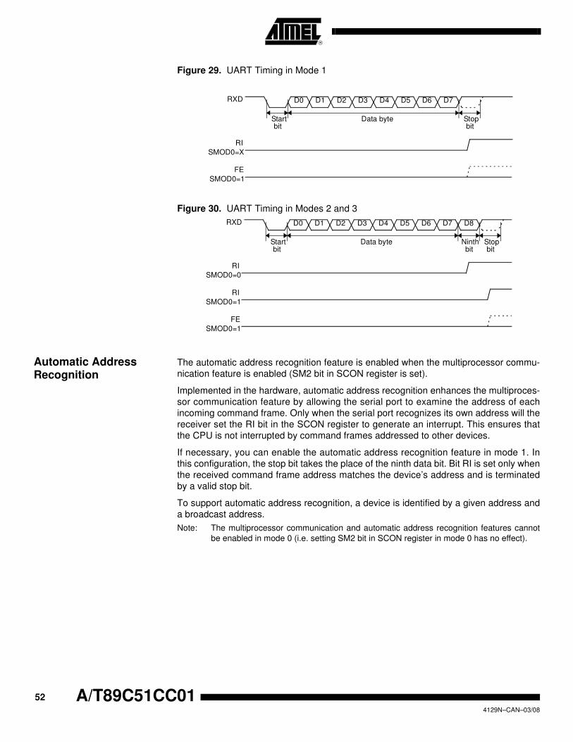
52 A/T89C51CC014129N–CAN–03/08
Figure 29. UART Timing in Mode 1
Figure 30. UART Timing in Modes 2 and 3
Automatic Address Recognition
The automatic address recognition feature is enabled when the multiprocessor commu-
nication feature is enabled (SM2 bit in SCON register is set).
Implemented in the hardware, automatic address recognition enhances the multiproces-
sor communication feature by allowing the serial port to examine the address of each
incoming command frame. Only when the serial port recognizes its own address will the
receiver set the RI bit in the SCON register to generate an interrupt. This ensures that
the CPU is not interrupted by command frames addressed to other devices.
If necessary, you can enable the automatic address recognition feature in mode 1. In
this configuration, the stop bit takes the place of the ninth data bit. Bit RI is set only when
the received command frame address matches the device’s address and is terminated
by a valid stop bit.
To support automatic address recognition, a device is identified by a given address and
a broadcast address.
Note: The multiprocessor communication and automatic address recognition features cannot
be enabled in mode 0 (i.e. setting SM2 bit in SCON register in mode 0 has no effect).
Data byte
RI
SMOD0=X
Stopbit
Startbit
RXD D7D6D5D4D3D2D1D0
FE
SMOD0=1
RI
SMOD0=0
Data byte Ninthbit
Stopbit
Startbit
RXD D8D7D6D5D4D3D2D1D0
RI
SMOD0=1
FE
SMOD0=1

53
A/T89C51CC01
4129N–CAN–03/08
Given Address Each device has an individual address that is specified in the SADDR register; the
SADEN register is a mask byte that contains don’t-care bits (defined by zeros) to form
the device’s given address. The don’t-care bits provide the flexibility to address one or
more slaves at a time. The following example illustrates how a given address is formed.
To address a device by its individual address, the SADEN mask byte must be 1111
1111b.
For example:SADDR0101 0110b
SADEN1111 1100b
Given0101 01XXb
Here is an example of how to use given addresses to address different slaves:Slave A:SADDR1111 0001b
SADEN1111 1010b
Given1111 0X0Xb
Slave B:SADDR1111 0011b
SADEN1111 1001b
Given1111 0XX1b
Slave C:SADDR1111 0011b
SADEN1111 1101b
Given1111 00X1b
The SADEN byte is selected so that each slave may be addressed separately.
For slave A, bit 0 (the LSB) is a don’t-care bit; for slaves B and C, bit 0 is a 1. To com-
municate with slave A only, the master must send an address where bit 0 is clear (e.g.
1111 0000b).
For slave A, bit 1 is a 0; for slaves B and C, bit 1 is a don’t care bit. To communicate with
slaves A and B, but not slave C, the master must send an address with bits 0 and 1 both
set (e.g. 1111 0011b).
To communicate with slaves A, B and C, the master must send an address with bit 0 set,
bit 1 clear, and bit 2 clear (e.g. 1111 0001b).
Broadcast Address A broadcast address is formed from the logical OR of the SADDR and SADEN registers
with zeros defined as don’t-care bits, e.g.:SADDR 0101 0110b
SADEN 1111 1100b
SADDR OR SADEN1111 111Xb
The use of don’t-care bits provides flexibility in defining the broadcast address, however
in most applications, a broadcast address is FFh. The following is an example of using
broadcast addresses:Slave A:SADDR1111 0001b
SADEN1111 1010b
Given1111 1X11b,
Slave B:SADDR1111 0011b
SADEN1111 1001b
Given1111 1X11B,
Slave C:SADDR=1111 0010b
SADEN1111 1101b
Given1111 1111b
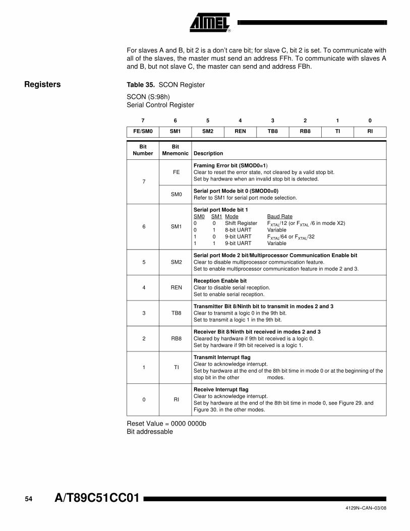
54 A/T89C51CC014129N–CAN–03/08
For slaves A and B, bit 2 is a don’t care bit; for slave C, bit 2 is set. To communicate with
all of the slaves, the master must send an address FFh. To communicate with slaves A
and B, but not slave C, the master can send and address FBh.
Registers Table 35. SCON Register
SCON (S:98h)
Serial Control Register
Reset Value = 0000 0000b
Bit addressable
7 6 5 4 3 2 1 0
FE/SM0 SM1 SM2 REN TB8 RB8 TI RI
Bit
Number
Bit
Mnemonic Description
7
FE
Framing Error bit (SMOD0=1)
Clear to reset the error state, not cleared by a valid stop bit.
Set by hardware when an invalid stop bit is detected.
SM0Serial port Mode bit 0 (SMOD0=0)
Refer to SM1 for serial port mode selection.
6 SM1
Serial port Mode bit 1
SM0 SM1 Mode Baud Rate
0 0 Shift Register FXTAL/12 (or FXTAL /6 in mode X2)
0 1 8-bit UART Variable
1 0 9-bit UART FXTAL/64 or FXTAL/32
1 1 9-bit UART Variable
5 SM2
Serial port Mode 2 bit/Multiprocessor Communication Enable bit
Clear to disable multiprocessor communication feature.
Set to enable multiprocessor communication feature in mode 2 and 3.
4 REN
Reception Enable bit
Clear to disable serial reception.
Set to enable serial reception.
3 TB8
Transmitter Bit 8/Ninth bit to transmit in modes 2 and 3
Clear to transmit a logic 0 in the 9th bit.
Set to transmit a logic 1 in the 9th bit.
2 RB8
Receiver Bit 8/Ninth bit received in modes 2 and 3
Cleared by hardware if 9th bit received is a logic 0.
Set by hardware if 9th bit received is a logic 1.
1 TI
Transmit Interrupt flag
Clear to acknowledge interrupt.
Set by hardware at the end of the 8th bit time in mode 0 or at the beginning of the
stop bit in the other modes.
0 RI
Receive Interrupt flag
Clear to acknowledge interrupt.
Set by hardware at the end of the 8th bit time in mode 0, see Figure 29. and
Figure 30. in the other modes.

55
A/T89C51CC01
4129N–CAN–03/08
Table 36. SADEN Register
SADEN (S:B9h)
Slave Address Mask Register
Reset Value = 0000 0000b
Not bit addressable
Table 37. SADDR Register
SADDR (S:A9h)
Slave Address Register
Reset Value = 0000 0000b
Not bit addressable
Table 38. SBUF Register
SBUF (S:99h)
Serial Data Buffer
Reset Value = 0000 0000b
Not bit addressable
7 6 5 4 3 2 1 0
– – – – – – – –
Bit
Number
Bit
Mnemonic Description
7-0 Mask Data for Slave Individual Address
7 6 5 4 3 2 1 0
– – – – – – – –
Bit
Number
Bit
Mnemonic Description
7-0 Slave Individual Address
7 6 5 4 3 2 1 0
– – – – – – – –
Bit
Number
Bit
Mnemonic Description
7-0 Data sent/received by Serial I/O Port

56 A/T89C51CC014129N–CAN–03/08
Table 39. PCON Register
PCON (S:87h)
Power Control Register
Reset Value = 00X1 0000b
Not bit addressable
7 6 5 4 3 2 1 0
SMOD1 SMOD0 – POF GF1 GF0 PD IDL
Bit
Number
Bit
Mnemonic Description
7 SMOD1Serial port Mode bit 1
Set to select double baud rate in mode 1, 2 or 3.
6 SMOD0
Serial port Mode bit 0
Clear to select SM0 bit in SCON register.
Set to select FE bit in SCON register.
5 -Reserved
The value read from this bit is indeterminate. Do not set this bit.
4 POF
Power-Off Flag
Clear to recognize next reset type.
Set by hardware when VCC rises from 0 to its nominal voltage. Can also be set
by software.
3 GF1
General-purpose Flag
Cleared by user for general-purpose usage.
Set by user for general-purpose usage.
2 GF0
General-purpose Flag
Cleared by user for general-purpose usage.
Set by user for general-purpose usage.
1 PD
Power-Down mode bit
Cleared by hardware when reset occurs.
Set to enter power-down mode.
0 IDL
Idle mode bit
Clear by hardware when interrupt or reset occurs.
Set to enter idle mode.

57
A/T89C51CC01
4129N–CAN–03/08
Timers/Counters The T89C51CC01 implements two general-purpose, 16-bit Timers/Counters. Such are
identified as Timer 0 and Timer 1, and can be independently configured to operate in a
variety of modes as a Timer or an event Counter. When operating as a Timer, the
Timer/Counter runs for a programmed length of time, then issues an interrupt request.
When operating as a Counter, the Timer/Counter counts negative transitions on an
external pin. After a preset number of counts, the Counter issues an interrupt request.
The various operating modes of each Timer/Counter are described in the following
sections.
Timer/Counter Operations
A basic operation is Timer registers THx and TLx (x = 0, 1) connected in cascade to
form a 16-bit Timer. Setting the run control bit (TRx) in TCON register (see Figure 40)
turns the Timer on by allowing the selected input to increment TLx. When TLx overflows
it increments THx; when THx overflows it sets the Timer overflow flag (TFx) in TCON
register. Setting the TRx does not clear the THx and TLx Timer registers. Timer regis-
ters can be accessed to obtain the current count or to enter preset values. They can be
read at any time but TRx bit must be cleared to preset their values, otherwise the behav-
ior of the Timer/Counter is unpredictable.
The C/Tx# control bit selects Timer operation or Counter operation by selecting the
divided-down peripheral clock or external pin Tx as the source for the counted signal.
TRx bit must be cleared when changing the mode of operation, otherwise the behavior
of the Timer/Counter is unpredictable.
For Timer operation (C/Tx# = 0), the Timer register counts the divided-down peripheral
clock. The Timer register is incremented once every peripheral cycle (6 peripheral clock
periods). The Timer clock rate is FPER/6, i.e. FOSC/12 in standard mode or FOSC/6 in X2
mode.
For Counter operation (C/Tx# = 1), the Timer register counts the negative transitions on
the Tx external input pin. The external input is sampled every peripheral cycles. When
the sample is high in one cycle and low in the next one, the Counter is incremented.
Since it takes 2 cycles (12 peripheral clock periods) to recognize a negative transition,
the maximum count rate is FPER/12, i.e. FOSC/24 in standard mode or FOSC/12 in X2
mode. There are no restrictions on the duty cycle of the external input signal, but to
ensure that a given level is sampled at least once before it changes, it should be held for
at least one full peripheral cycle.
Timer 0 Timer 0 functions as either a Timer or event Counter in four modes of operation.
Figure 31 to Figure 34 show the logical configuration of each mode.
Timer 0 is controlled by the four lower bits of TMOD register (see Figure 41) and bits 0,
1, 4 and 5 of TCON register (see Figure 40). TMOD register selects the method of Timer
gating (GATE0), Timer or Counter operation (T/C0#) and mode of operation (M10 and
M00). TCON register provides Timer 0 control functions: overflow flag (TF0), run control
bit (TR0), interrupt flag (IE0) and interrupt type control bit (IT0).
For normal Timer operation (GATE0 = 0), setting TR0 allows TL0 to be incremented by
the selected input. Setting GATE0 and TR0 allows external pin INT0# to control Timer
operation.
Timer 0 overflow (count rolls over from all 1s to all 0s) sets TF0 flag generating an inter-
rupt request.
It is important to stop Timer/Counter before changing mode.
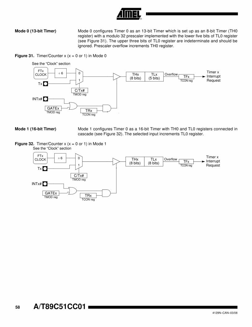
58 A/T89C51CC014129N–CAN–03/08
Mode 0 (13-bit Timer) Mode 0 configures Timer 0 as an 13-bit Timer which is set up as an 8-bit Timer (TH0
register) with a modulo 32 prescaler implemented with the lower five bits of TL0 register
(see Figure 31). The upper three bits of TL0 register are indeterminate and should be
ignored. Prescaler overflow increments TH0 register.
Figure 31. Timer/Counter x (x = 0 or 1) in Mode 0
Mode 1 (16-bit Timer) Mode 1 configures Timer 0 as a 16-bit Timer with TH0 and TL0 registers connected in
cascade (see Figure 32). The selected input increments TL0 register.
Figure 32. Timer/Counter x (x = 0 or 1) in Mode 1
FTxCLOCK
TRxTCON reg
TFxTCON reg
0
1
GATExTMOD reg
÷ 6 OverflowTimer xInterruptRequest
C/Tx#TMOD reg
TLx(5 bits)
THx(8 bits)
INTx#
Tx
See the “Clock” section
TRxTCON reg
TFxTCON reg
0
1
GATExTMOD reg
OverflowTimer xInterruptRequest
C/Tx#TMOD reg
TLx(8 bits)
THx(8 bits)
INTx#
Tx
FTxCLOCK ÷ 6
See the “Clock” section

59
A/T89C51CC01
4129N–CAN–03/08
Mode 2 (8-bit Timer with Auto-
Reload)
Mode 2 configures Timer 0 as an 8-bit Timer (TL0 register) that automatically reloads
from TH0 register (see Figure 33). TL0 overflow sets TF0 flag in TCON register and
reloads TL0 with the contents of TH0, which is preset by software. When the interrupt
request is serviced, hardware clears TF0. The reload leaves TH0 unchanged. The next
reload value may be changed at any time by writing it to TH0 register.
Figure 33. Timer/Counter x (x = 0 or 1) in Mode 2
Mode 3 (Two 8-bit Timers) Mode 3 configures Timer 0 such that registers TL0 and TH0 operate as separate 8-bit
Timers (see Figure 34). This mode is provided for applications requiring an additional 8-
bit Timer or Counter. TL0 uses the Timer 0 control bits C/T0# and GATE0 in TMOD reg-
ister, and TR0 and TF0 in TCON register in the normal manner. TH0 is locked into a
Timer function (counting FPER /6) and takes over use of the Timer 1 interrupt (TF1) and
run control (TR1) bits. Thus, operation of Timer 1 is restricted when Timer 0 is in mode
3.
Figure 34. Timer/Counter 0 in Mode 3: Two 8-bit Counters
TRxTCON reg
TFxTCON reg
0
1
GATExTMOD reg
OverflowTimer xInterruptRequest
C/Tx#TMOD reg
TLx(8 bits)
THx(8 bits)
INTx#
Tx
FTxCLOCK ÷ 6
See the “Clock” section
TR0TCON.4
TF0TCON.5
INT0#
0
1
GATE0TMOD.3
OverflowTimer 0InterruptRequest
C/T0#TMOD.2
TL0(8 bits)
TR1TCON.6
TH0(8 bits) TF1
TCON.7
OverflowTimer 1InterruptRequest
T0
FTxCLOCK ÷ 6
FTxCLOCK ÷ 6
See the “Clock” section

60 A/T89C51CC014129N–CAN–03/08
Timer 1 Timer 1 is identical to Timer 0 excepted for Mode 3 which is a hold-count mode. The fol-
lowing comments help to understand the differences:
• Timer 1 functions as either a Timer or event Counter in three modes of operation.
Figure 31 to Figure 33 show the logical configuration for modes 0, 1, and 2. Timer
1’s mode 3 is a hold-count mode.
• Timer 1 is controlled by the four high-order bits of TMOD register (see Figure 41)
and bits 2, 3, 6 and 7 of TCON register (see Figure 40). TMOD register selects the
method of Timer gating (GATE1), Timer or Counter operation (C/T1#) and mode of
operation (M11 and M01). TCON register provides Timer 1 control functions:
overflow flag (TF1), run control bit (TR1), interrupt flag (IE1) and interrupt type
control bit (IT1).
• Timer 1 can serve as the Baud Rate Generator for the Serial Port. Mode 2 is best
suited for this purpose.
• For normal Timer operation (GATE1 = 0), setting TR1 allows TL1 to be incremented
by the selected input. Setting GATE1 and TR1 allows external pin INT1# to control
Timer operation.
• Timer 1 overflow (count rolls over from all 1s to all 0s) sets the TF1 flag generating
an interrupt request.
• When Timer 0 is in mode 3, it uses Timer 1’s overflow flag (TF1) and run control bit
(TR1). For this situation, use Timer 1 only for applications that do not require an
interrupt (such as a Baud Rate Generator for the Serial Port) and switch Timer 1 in
and out of mode 3 to turn it off and on.
• It is important to stop Timer/Counter before changing mode.
Mode 0 (13-bit Timer) Mode 0 configures Timer 1 as a 13-bit Timer, which is set up as an 8-bit Timer (TH1 reg-
ister) with a modulo-32 prescaler implemented with the lower 5 bits of the TL1 register
(see Figure 31). The upper 3 bits of TL1 register are ignored. Prescaler overflow incre-
ments TH1 register.
Mode 1 (16-bit Timer) Mode 1 configures Timer 1 as a 16-bit Timer with TH1 and TL1 registers connected in
cascade (see Figure 32). The selected input increments TL1 register.
Mode 2 (8-bit Timer with Auto-
Reload)
Mode 2 configures Timer 1 as an 8-bit Timer (TL1 register) with automatic reload from
TH1 register on overflow (see Figure 33). TL1 overflow sets TF1 flag in TCON register
and reloads TL1 with the contents of TH1, which is preset by software. The reload
leaves TH1 unchanged.
Mode 3 (Halt) Placing Timer 1 in mode 3 causes it to halt and hold its count. This can be used to halt
Timer 1 when TR1 run control bit is not available i.e. when Timer 0 is in mode 3.
Interrupt Each Timer handles one interrupt source that is the timer overflow flag TF0 or TF1. This
flag is set every time an overflow occurs. Flags are cleared when vectoring to the Timer
interrupt routine. Interrupts are enabled by setting ETx bit in IEN0 register. This assumes
interrupts are globally enabled by setting EA bit in IEN0 register.

61
A/T89C51CC01
4129N–CAN–03/08
Figure 35. Timer Interrupt System
TF0TCON.5
ET0IEN0.1
Timer 0Interrupt Request
TF1TCON.7
ET1IEN0.3
Timer 1Interrupt Request

62 A/T89C51CC014129N–CAN–03/08
Registers Table 40. TCON Register
TCON (S:88h)
Timer/Counter Control Register
Reset Value = 0000 0000b
7 6 5 4 3 2 1 0
TF1 TR1 TF0 TR0 IE1 IT1 IE0 IT0
Bit
Number
Bit
Mnemonic Description
7 TF1
Timer 1 Overflow Flag
Cleared by hardware when processor vectors to interrupt routine.
Set by hardware on Timer/Counter overflow, when Timer 1 register overflows.
6 TR1
Timer 1 Run Control Bit
Clear to turn off Timer/Counter 1.
Set to turn on Timer/Counter 1.
5 TF0
Timer 0 Overflow Flag
Cleared by hardware when processor vectors to interrupt routine.
Set by hardware on Timer/Counter overflow, when Timer 0 register overflows.
4 TR0
Timer 0 Run Control Bit
Clear to turn off Timer/Counter 0.
Set to turn on Timer/Counter 0.
3 IE1
Interrupt 1 Edge Flag
Cleared by hardware when interrupt is processed if edge-triggered (see IT1).
Set by hardware when external interrupt is detected on INT1# pin.
2 IT1
Interrupt 1 Type Control Bit
Clear to select low level active (level triggered) for external interrupt 1 (INT1#).
Set to select falling edge active (edge triggered) for external interrupt 1.
1 IE0
Interrupt 0 Edge Flag
Cleared by hardware when interrupt is processed if edge-triggered (see IT0).
Set by hardware when external interrupt is detected on INT0# pin.
0 IT0
Interrupt 0 Type Control Bit
Clear to select low level active (level triggered) for external interrupt 0 (INT0#).
Set to select falling edge active (edge triggered) for external interrupt 0.

63
A/T89C51CC01
4129N–CAN–03/08
Table 41. TMOD Register
TMOD (S:89h)
Timer/Counter Mode Control Register
Notes: 1. Reloaded from TH1 at overflow.
2. Reloaded from TH0 at overflow.
Reset Value = 0000 0000b
7 6 5 4 3 2 1 0
GATE1 C/T1# M11 M01 GATE0 C/T0# M10 M00
Bit
Number
Bit
Mnemonic Description
7 GATE1
Timer 1 Gating Control Bit
Clear to enable Timer 1 whenever TR1 bit is set.
Set to enable Timer 1 only while INT1# pin is high and TR1 bit is set.
6 C/T1#
Timer 1 Counter/Timer Select Bit
Clear for Timer operation: Timer 1 counts the divided-down system clock.
Set for Counter operation: Timer 1 counts negative transitions on external pin T1.
5 M11 Timer 1 Mode Select Bits
M11 M01 Operating mode
0 0 Mode 0: 8-bit Timer/Counter (TH1) with 5-bit prescaler (TL1).
0 1 Mode 1: 16-bit Timer/Counter.
1 0 Mode 2: 8-bit auto-reload Timer/Counter (TL1)(1)
1 1 Mode 3: Timer 1 halted. Retains count
4 M01
3 GATE0
Timer 0 Gating Control Bit
Clear to enable Timer 0 whenever TR0 bit is set.
Set to enable Timer/Counter 0 only while INT0# pin is high and TR0 bit is set.
2 C/T0#
Timer 0 Counter/Timer Select Bit
Clear for Timer operation: Timer 0 counts the divided-down system clock.
Set for Counter operation: Timer 0 counts negative transitions on external pin T0.
1 M10
Timer 0 Mode Select Bit
M10 M00 Operating mode
0 0 Mode 0: 8-bit Timer/Counter (TH0) with 5-bit prescaler (TL0).
0 1 Mode 1: 16-bit Timer/Counter.
1 0 Mode 2: 8-bit auto-reload Timer/Counter (TL0)(2)
1 1 Mode 3: TL0 is an 8-bit Timer/Counter
TH0 is an 8-bit Timer using Timer 1’s TR0 and TF0 bits.
0 M00

64 A/T89C51CC014129N–CAN–03/08
Table 42. TH0 Register
TH0 (S:8Ch)
Timer 0 High Byte Register
Reset Value = 0000 0000b
Table 43. TL0 Register
TL0 (S:8Ah)
Timer 0 Low Byte Register
Reset Value = 0000 0000b
Table 44. TH1 Register
TH1 (S:8Dh)
Timer 1 High Byte Register
Reset Value = 0000 0000b
7 6 5 4 3 2 1 0
– – – – – – – –
Bit
Number
Bit
Mnemonic Description
7:0 High Byte of Timer 0.
7 6 5 4 3 2 1 0
– – – – – – – –
Bit
Number
Bit
Mnemonic Description
7:0 Low Byte of Timer 0.
7 6 5 4 3 2 1 0
– – – – – – – –
Bit
Number
Bit
Mnemonic Description
7:0 High Byte of Timer 1.

65
A/T89C51CC01
4129N–CAN–03/08
Table 45. TL1 Register
TL1 (S:8Bh)
Timer 1 Low Byte Register
Reset Value = 0000 0000b
7 6 5 4 3 2 1 0
– – – – – – – –
Bit
Number
Bit
Mnemonic Description
7:0 Low Byte of Timer 1.
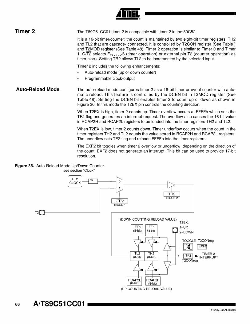
66 A/T89C51CC014129N–CAN–03/08
Timer 2 The T89C51CC01 timer 2 is compatible with timer 2 in the 80C52.
It is a 16-bit timer/counter: the count is maintained by two eight-bit timer registers, TH2
and TL2 that are cascade- connected. It is controlled by T2CON register (See Table )
and T2MOD register (See Table 48). Timer 2 operation is similar to Timer 0 and Timer
1. C/T2 selects FT2 clock/6 (timer operation) or external pin T2 (counter operation) as
timer clock. Setting TR2 allows TL2 to be incremented by the selected input.
Timer 2 includes the following enhancements:
• Auto-reload mode (up or down counter)
• Programmable clock-output
Auto-Reload Mode The auto-reload mode configures timer 2 as a 16-bit timer or event counter with auto-
matic reload. This feature is controlled by the DCEN bit in T2MOD register (See
Table 48). Setting the DCEN bit enables timer 2 to count up or down as shown in
Figure 36. In this mode the T2EX pin controls the counting direction.
When T2EX is high, timer 2 counts up. Timer overflow occurs at FFFFh which sets the
TF2 flag and generates an interrupt request. The overflow also causes the 16-bit value
in RCAP2H and RCAP2L registers to be loaded into the timer registers TH2 and TL2.
When T2EX is low, timer 2 counts down. Timer underflow occurs when the count in the
timer registers TH2 and TL2 equals the value stored in RCAP2H and RCAP2L registers.
The underflow sets TF2 flag and reloads FFFFh into the timer registers.
The EXF2 bit toggles when timer 2 overflow or underflow, depending on the direction of
the count. EXF2 does not generate an interrupt. This bit can be used to provide 17-bit
resolution.
Figure 36. Auto-Reload Mode Up/Down Counter
(DOWN COUNTING RELOAD VALUE)
TF2
T2
EXF2
TH2(8-bit)
TL2(8-bit)
RCAP2H(8-bit)
RCAP2L(8-bit)
FFh(8-bit)
FFh(8-bit)
TOGGLE
(UP COUNTING RELOAD VALUE)
TIMER 2INTERRUPT
:6
T2CONreg
T2CONreg
T2EX:
1=UP
2=DOWN
0
1
CT/2T2CON.1
TR2T2CON.2
FT2CLOCK
see section “Clock”
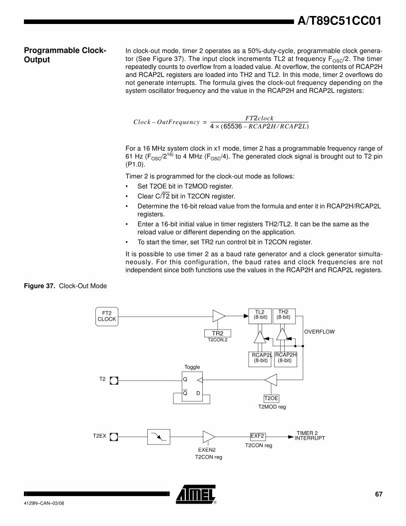
67
A/T89C51CC01
4129N–CAN–03/08
Programmable Clock-Output
In clock-out mode, timer 2 operates as a 50%-duty-cycle, programmable clock genera-
tor (See Figure 37). The input clock increments TL2 at frequency FOSC/2. The timer
repeatedly counts to overflow from a loaded value. At overflow, the contents of RCAP2H
and RCAP2L registers are loaded into TH2 and TL2. In this mode, timer 2 overflows do
not generate interrupts. The formula gives the clock-out frequency depending on the
system oscillator frequency and the value in the RCAP2H and RCAP2L registers:
For a 16 MHz system clock in x1 mode, timer 2 has a programmable frequency range of
61 Hz (FOSC/216) to 4 MHz (FOSC/4). The generated clock signal is brought out to T2 pin
(P1.0).
Timer 2 is programmed for the clock-out mode as follows:
• Set T2OE bit in T2MOD register.
• Clear C/T2 bit in T2CON register.
• Determine the 16-bit reload value from the formula and enter it in RCAP2H/RCAP2L
registers.
• Enter a 16-bit initial value in timer registers TH2/TL2. It can be the same as the
reload value or different depending on the application.
• To start the timer, set TR2 run control bit in T2CON register.
It is possible to use timer 2 as a baud rate generator and a clock generator simulta-
neously. For this configuration, the baud rates and clock frequencies are not
independent since both functions use the values in the RCAP2H and RCAP2L registers.
Figure 37. Clock-Out Mode
Clock OutFrequency–FT2clock
4 65536 RCAP2H– RCAP2L⁄( )×-----------------------------------------------------------------------------------------=
EXEN2
EXF2
OVERFLOW
T2EX
TH2(8-bit)
TL2(8-bit)
TIMER 2
RCAP2H(8-bit)
RCAP2L(8-bit)
T2OE
T2CON reg
T2CON reg
T2MOD reg
INTERRUPT
TR2T2CON.2
FT2CLOCK
T2
Q D
Toggle
Q

68 A/T89C51CC014129N–CAN–03/08
Registers Table 46. T2CON Register
T2CON (S:C8h)
Timer 2 Control Register
Reset Value = 0000 0000b
Bit addressable
7 6 5 4 3 2 1 0
TF2 EXF2 RCLK TCLK EXEN2 TR2 C/T2# CP/RL2#
Bit
Number
Bit
Mnemonic Description
7 TF2
Timer 2 Overflow Flag
TF2 is not set if RCLK=1 or TCLK = 1.
Must be cleared by software.
Set by hardware on timer 2 overflow.
6 EXF2
Timer 2 External Flag
Set when a capture or a reload is caused by a negative transition on T2EX pin if
EXEN2=1.
Set to cause the CPU to vector to timer 2 interrupt routine when timer 2 interrupt
is enabled.
Must be cleared by software.
5 RCLK
Receive Clock bit
Clear to use timer 1 overflow as receive clock for serial port in mode 1 or 3.
Set to use timer 2 overflow as receive clock for serial port in mode 1 or 3.
4 TCLK
Transmit Clock bit
Clear to use timer 1 overflow as transmit clock for serial port in mode 1 or 3.
Set to use timer 2 overflow as transmit clock for serial port in mode 1 or 3.
3 EXEN2
Timer 2 External Enable bit
Clear to ignore events on T2EX pin for timer 2 operation.
Set to cause a capture or reload when a negative transition on T2EX pin is
detected, if timer 2 is not used to clock the serial port.
2 TR2
Timer 2 Run Control bit
Clear to turn off timer 2.
Set to turn on timer 2.
1 C/T2#
Timer/Counter 2 Select bit
Clear for timer operation (input from internal clock system: FOSC).
Set for counter operation (input from T2 input pin).
0 CP/RL2#
Timer 2 Capture/Reload bit
If RCLK=1 or TCLK=1, CP/RL2# is ignored and timer is forced to auto-reload on
timer 2 overflow.
Clear to auto-reload on timer 2 overflows or negative transitions on T2EX pin if
EXEN2=1.
Set to capture on negative transitions on T2EX pin if EXEN2=1.

69
A/T89C51CC01
4129N–CAN–03/08
Table 47. T2MOD Register
T2MOD (S:C9h)
Timer 2 Mode Control Register
Reset Value = XXXX XX00b
Not bit addressable
Table 48. TH2 Register
TH2 (S:CDh)
Timer 2 High Byte Register
Reset Value = 0000 0000b
Not bit addressable
7 6 5 4 3 2 1 0
- - - - - - T2OE DCEN
Bit
Number
Bit
Mnemonic Description
7 -Reserved
The value read from this bit is indeterminate. Do not set this bit.
6 -Reserved
The value read from this bit is indeterminate. Do not set this bit.
5 -Reserved
The value read from this bit is indeterminate. Do not set this bit.
4 -Reserved
The value read from this bit is indeterminate. Do not set this bit.
3 -Reserved
The value read from this bit is indeterminate. Do not set this bit.
2 -Reserved
The value read from this bit is indeterminate. Do not set this bit.
1 T2OE
Timer 2 Output Enable bit
Clear to program P1.0/T2 as clock input or I/O port.
Set to program P1.0/T2 as clock output.
0 DCEN
Down Counter Enable bit
Clear to disable timer 2 as up/down counter.
Set to enable timer 2 as up/down counter.
7 6 5 4 3 2 1 0
- - - - - - - -
Bit
Number
Bit
Mnemonic Description
7-0 High Byte of Timer 2.

70 A/T89C51CC014129N–CAN–03/08
Table 49. TL2 Register
TL2 (S:CCh)
Timer 2 Low Byte Register
Reset Value = 0000 0000b
Not bit addressable
Table 50. RCAP2H Register
RCAP2H (S:CBh)
Timer 2 Reload/Capture High Byte Register
Reset Value = 0000 0000b
Not bit addressable
Table 51. RCAP2L Register
RCAP2L (S:CAH)
TIMER 2 REload/Capture Low Byte Register
Reset Value = 0000 0000b
Not bit addressable
7 6 5 4 3 2 1 0
- - - - - - - -
Bit
Number
Bit
Mnemonic Description
7-0 Low Byte of Timer 2.
7 6 5 4 3 2 1 0
- - - - - - - -
Bit
Number
Bit
Mnemonic Description
7-0 High Byte of Timer 2 Reload/Capture.
7 6 5 4 3 2 1 0
- - - - - - - -
Bit
Number
Bit
Mnemonic Description
7-0 Low Byte of Timer 2 Reload/Capture.

71
A/T89C51CC01
4129N–CAN–03/08
Watchdog Timer T89C51CC01 contains a powerful programmable hardware Watchdog Timer (WDT) that
automatically resets the chip if it software fails to reset the WDT before the selected time
interval has elapsed. It permits large Time-Out ranking from 16ms to 2s @Fosc =
12MHz in X1 mode.
This WDT consists of a 14-bit counter plus a 7-bit programmable counter, a Watchdog
Timer reset register (WDTRST) and a Watchdog Timer programming (WDTPRG) regis-
ter. When exiting reset, the WDT is -by default- disable.
To enable the WDT, the user has to write the sequence 1EH and E1H into WDTRST
register no instruction in between. When the Watchdog Timer is enabled, it will incre-
ment every machine cycle while the oscillator is running and there is no way to disable
the WDT except through reset (either hardware reset or WDT overflow reset). When
WDT overflows, it will generate an output RESET pulse at the RST pin. The RESET
pulse duration is 96xTOSC, where TOSC=1/FOSC. To make the best use of the WDT, it
should be serviced in those sections of code that will periodically be executed within the
time required to prevent a WDT reset
Note: When the Watchdog is enable it is impossible to change its period.
Figure 38. Watchdog Timer
WDTPRG
RESETDecoder
Control
WDTRST
WR
Enable
14-bit COUNTER 7-bit COUNTER
Outputs
RESET
- - - - - 2 1 0
Fwd Clock

72 A/T89C51CC014129N–CAN–03/08
Watchdog Programming The three lower bits (S0, S1, S2) located into WDTPRG register permit to program the
WDT duration.
Table 52. Machine Cycle Count
To compute WD Time-Out, the following formula is applied:
Note: Svalue represents the decimal value of (S2 S1 S0)
The following table outlines the time-out value for FoscXTAL = 12 MHz in X1 mode
Table 53. Time-Out Computation
S2 S1 S0 Machine Cycle Count
0 0 0 214 - 1
0 0 1 215 - 1
0 1 0 216 - 1
0 1 1 217 - 1
1 0 0 218 - 1
1 0 1 219 - 1
1 1 0 220 - 1
1 1 1 221 - 1
S2 S1 S0 Fosc = 12 MHz Fosc = 16 MHz Fosc = 20 MHz
0 0 0 16.38 ms 12.28 ms 9.82 ms
0 0 1 32.77 ms 24.57 ms 19.66 ms
0 1 0 65.54 ms 49.14 ms 39.32 ms
0 1 1 131.07 ms 98.28 ms 78.64 ms
1 0 0 262.14 ms 196.56 ms 157.28 ms
1 0 1 524.29 ms 393.12 ms 314.56 ms
1 1 0 1.05 s 786.24 ms 629.12 ms
1 1 1 2.10 s 1.57 s 1.25 s
FTime OutFosc
6 2×WDX2 X2∧
214
2Svalue
×( )
-----------------------------------------------------------------------------=–

73
A/T89C51CC01
4129N–CAN–03/08
Watchdog Timer During Power-down Mode and Idle
In Power-down mode the oscillator stops, which means the WDT also stops. While in
Power-down mode, the user does not need to service the WDT. There are 2 methods of
exiting Power-down mode: by a hardware reset or via a level activated external interrupt
which is enabled prior to entering Power-down mode. When Power-down is exited with
hardware reset, the Watchdog is disabled. Exiting Power-down with an interrupt is sig-
nificantly different. The interrupt shall be held low long enough for the oscillator to
stabilize. When the interrupt is brought high, the interrupt is serviced. To prevent the
WDT from resetting the device while the interrupt pin is held low, the WDT is not started
until the interrupt is pulled high. It is suggested that the WDT be reset during the inter-
rupt service for the interrupt used to exit Power-down.
To ensure that the WDT does not overflow within a few states of exiting powerdown, it is
best to reset the WDT just before entering powerdown.
In the Idle mode, the oscillator continues to run. To prevent the WDT from resetting
T89C51CC01 while in Idle mode, the user should always set up a timer that will periodi-
cally exit Idle, service the WDT, and re-enter Idle mode.
Register Table 54. WDTPRG Register
WDTPRG (S:A7h)
Watchdog Timer Duration Programming Register
Reset Value = XXXX X000b
7 6 5 4 3 2 1 0
– – – – – S2 S1 S0
Bit
Number
Bit
Mnemonic Description
7 -Reserved
The value read from this bit is indeterminate. Do not set this bit.
6 -Reserved
The value read from this bit is indeterminate. Do not set this bit.
5 -Reserved
The value read from this bit is indeterminate. Do not set this bit.
4 -Reserved
The value read from this bit is indeterminate. Do not set this bit.
3 -Reserved
The value read from this bit is indeterminate. Do not set this bit.
2 S2Watchdog Timer Duration selection bit 2
Work in conjunction with bit 1 and bit 0.
1 S1Watchdog Timer Duration selection bit 1
Work in conjunction with bit 2 and bit 0.
0 S0Watchdog Timer Duration selection bit 0
Work in conjunction with bit 1 and bit 2.
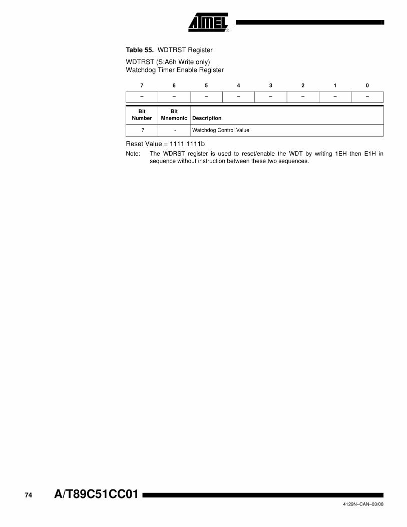
74 A/T89C51CC014129N–CAN–03/08
Table 55. WDTRST Register
WDTRST (S:A6h Write only)
Watchdog Timer Enable Register
Reset Value = 1111 1111b
Note: The WDRST register is used to reset/enable the WDT by writing 1EH then E1H in
sequence without instruction between these two sequences.
7 6 5 4 3 2 1 0
– – – – – – – –
Bit
Number
Bit
Mnemonic Description
7 - Watchdog Control Value

75
A/T89C51CC01
4129N–CAN–03/08
CAN Controller The CAN Controller provides all the features required to implement the serial communi-
cation protocol CAN as defined by BOSCH GmbH. The CAN specification as referred to
by ISO/11898 (2.0A and 2.0B) for high speed and ISO/11519-2 for low speed. The CAN
Controller is able to handle all types of frames (Data, Remote, Error and Overload) and
achieves a bitrate of 1-Mbit/sec. at 8 MHz1 Crystal frequency in X2 mode.
Note: 1. At BRP = 1 sampling point will be fixed.
CAN Protocol The CAN protocol is an international standard defined in the ISO 11898 for high speed
and ISO 11519-2 for low speed.
Principles CAN is based on a broadcast communication mechanism. This broadcast communica-
tion is achieved by using a message oriented transmission protocol. These messages
are identified by using a message identifier. Such a message identifier has to be unique
within the whole network and it defines not only the content but also the priority of the
message.
The priority at which a message is transmitted compared to another less urgent mes-
sage is specified by the identifier of each message. The priorities are laid down during
system design in the form of corresponding binary values and cannot be changed
dynamically. The identifier with the lowest binary number has the highest priority.
Bus access conflicts are resolved by bit-wise arbitration on the identifiers involved by
each node observing the bus level bit for bit. This happens in accordance with the "wired
and" mechanism, by which the dominant state overwrites the recessive state. The com-
petition for bus allocation is lost by all nodes with recessive transmission and dominant
observation. All the "losers" automatically become receivers of the message with the
highest priority and do not re-attempt transmission until the bus is available again.
Message Formats The CAN protocol supports two message frame formats, the only essential difference
being in the length of the identifier. The CAN standard frame, also known as CAN 2.0 A,
supports a length of 11 bits for the identifier, and the CAN extended frame, also known
as CAN 2.0 B, supports a length of 29 bits for the identifier.
Can Standard Frame
Figure 39. CAN Standard Frames
A message in the CAN standard frame format begins with the "Start Of Frame (SOF)",
this is followed by the "Arbitration field" which consist of the identifier and the "Remote
Transmission Request (RTR)" bit used to distinguish between the data frame and the
data request frame called remote frame. The following "Control field" contains the "IDen-
tifier Extension (IDE)" bit and the "Data Length Code (DLC)" used to indicate the
11-bit identifier ID10..0
Interframe Space
4-bit DLC DLC4..0
CRC del.
ACK del.
15-bit CRC0 - 8 bytesSOFSOF RTR IDE r0 ACK 7 bitsIntermission
3 bitsBus Idle Bus Idle
(Indefinite)
Arbitration Field
Data Field
Data Frame
Control Field
End of Frame
CRC Field
ACK Field
Interframe Space
11-bit identifier ID10..0
Interframe Space
4-bit DLC DLC4..0
CRC del.
ACK del.
15-bit CRCSOFSOF RTR IDE r0 ACK 7 bitsIntermission
3 bitsBus Idle Bus Idle
(Indefinite)
Arbitration Field
Remote Frame
Control Field
End of Frame
CRC Field
ACK Field
Interframe Space

76 A/T89C51CC014129N–CAN–03/08
number of following data bytes in the "Data field". In a remote frame, the DLC contains
the number of requested data bytes. The "Data field" that follows can hold up to 8 data
bytes. The frame integrity is guaranteed by the following "Cyclic Redundant Check
(CRC)" sum. The "ACKnowledge (ACK) field" compromises the ACK slot and the ACK
delimiter. The bit in the ACK slot is sent as a recessive bit and is overwritten as a domi-
nant bit by the receivers which have at this time received the data correctly. Correct
messages are acknowledged by the receivers regardless of the result of the acceptance
test. The end of the message is indicated by "End Of Frame (EOF)". The "Intermission
Frame Space (IFS)" is the minimum number of bits separating consecutive messages. If
there is no following bus access by any node, the bus remains idle.
CAN Extended Frame
Figure 40. CAN Extended Frames
A message in the CAN extended frame format is likely the same as a message in CAN
standard frame format. The difference is the length of the identifier used. The identifier is
made up of the existing 11-bit identifier (base identifier) and an 18-bit extension (identi-
fier extension). The distinction between CAN standard frame format and CAN extended
frame format is made by using the IDE bit which is transmitted as dominant in case of a
frame in CAN standard frame format, and transmitted as recessive in the other case.
Format Co-existence As the two formats have to co-exist on one bus, it is laid down which message has
higher priority on the bus in the case of bus access collision with different formats and
the same identifier / base identifier: The message in CAN standard frame format always
has priority over the message in extended format.
There are three different types of CAN modules available:
– 2.0A - Considers 29 bit ID as an error
– 2.0B Passive - Ignores 29 bit ID messages
– 2.0B Active - Handles both 11 and 29 bit ID Messages
Bit Timing To ensure correct sampling up to the last bit, a CAN node needs to re-synchronize
throughout the entire frame. This is done at the beginning of each message with the fall-
ing edge SOF and on each recessive to dominant edge.
Bit Construction One CAN bit time is specified as four non-overlapping time segments. Each segment is
constructed from an integer multiple of the Time Quantum. The Time Quantum or TQ is
the smallest discrete timing resolution used by a CAN node.
11-bit base identifier IDT28..18
Interframe Space
CRC del.
ACK del.
15-bit CRC0 - 8 bytesSOFSOF SRR IDE ACK 7 bitsIntermission
3 bitsBus Idle Bus Idle
(Indefinite)
Arbitration Field
Arbitration Field
Data Field
Data Frame
Control Field
Control Field
End of Frame
CRC Field
ACK Field
Interframe Space
11-bit base identifier IDT28..18
18-bit identifier extension ID17..0
18-bit identifier extension ID17..0
Interframe Space
4-bit DLC DLC4..0
CRC del.
ACK del.
15-bit CRCSOFSOF SRR IDE r0
4-bit DLC DLC4..0
RTR
RTR
r0r1
r1 ACK 7 bitsIntermission
3 bitsBus Idle Bus Idle
(Indefinite)
Remote Frame
End of Frame
CRC Field
ACK Field
Interframe Space

77
A/T89C51CC01
4129N–CAN–03/08
Figure 41. CAN Bit Construction
Synchronization Segment The first segment is used to synchronize the various bus nodes.
On transmission, at the start of this segment, the current bit level is output. If there is a
bit state change between the previous bit and the current bit, then the bus state change
is expected to occur within this segment by the receiving nodes.
Propagation Time Segment This segment is used to compensate for signal delays across the network.
This is necessary to compensate for signal propagation delays on the bus line and
through the transceivers of the bus nodes.
Phase Segment 1 Phase Segment 1 is used to compensate for edge phase errors.
This segment may be lengthened during resynchronization.
Sample Point The sample point is the point of time at which the bus level is read and interpreted as the
value of the respective bit. Its location is at the end of Phase Segment 1 (between the
two Phase Segments).
Phase Segment 2 This segment is also used to compensate for edge phase errors.
This segment may be shortened during resynchronization, but the length has to be at
least as long as the information processing time and may not be more than the length of
Phase Segment 1.
Information Processing Time It is the time required for the logic to determine the bit level of a sampled bit.
The Information processing Time begins at the sample point, is measured in TQ and is
fixed at 2 TQ for the Atmel CAN. Since Phase Segment 2 also begins at the sample
point and is the last segment in the bit time, Phase Segment 2 minimum shall not be
less than the Information processing Time.
Bit Lengthening As a result of resynchronization, Phase Segment 1 may be lengthened or Phase Seg-
ment 2 may be shortened to compensate for oscillator tolerances. If, for example, the
transmitter oscillator is slower than the receiver oscillator, the next falling edge used for
resynchronization may be delayed. So Phase Segment 1 is lengthened in order to
adjust the sample point and the end of the bit time.
Time Quantum (producer)
Nominal CAN Bit Time
Segments (producer)
SYNC_SEG PROP_SEG PHASE_SEG_1 PHASE_SEG_2
propagation
delay
Segments (consumer)
SYNC_SEG PROP_SEG PHASE_SEG_1 PHASE_SEG_2
Sample Point
Transmission Point (producer)
CAN Frame (producer)

78 A/T89C51CC014129N–CAN–03/08
Bit Shortening If, on the other hand, the transmitter oscillator is faster than the receiver one, the next
falling edge used for resynchronization may be too early. So Phase Segment 2 in bit N
is shortened in order to adjust the sample point for bit N+1 and the end of the bit time
Synchronization Jump Width The limit to the amount of lengthening or shortening of the Phase Segments is set by the
Resynchronization Jump Width.
This segment may not be longer than Phase Segment 2.
Programming the Sample Point Programming of the sample point allows "tuning" of the characteristics to suit the bus.
Early sampling allows more Time Quanta in the Phase Segment 2 so the Synchroniza-
tion Jump Width can be programmed to its maximum. This maximum capacity to
shorten or lengthen the bit time decreases the sensitivity to node oscillator tolerances,
so that lower cost oscillators such as ceramic resonators may be used.
Late sampling allows more Time Quanta in the Propagation Time Segment which allows
a poorer bus topology and maximum bus length.
Arbitration Figure 42. Bus Arbitration
The CAN protocol handles bus accesses according to the concept called “Carrier Sense
Multiple Access with Arbitration on Message Priority”.
During transmission, arbitration on the CAN bus can be lost to a competing device with
a higher priority CAN Identifier. This arbitration concept avoids collisions of messages
whose transmission was started by more than one node simultaneously and makes sure
the most important message is sent first without time loss.
The bus access conflict is resolved during the arbitration field mostly over the identifier
value. If a data frame and a remote frame with the same identifier are initiated at the
same time, the data frame prevails over the remote frame (c.f. RTR bit).
Errors The CAN protocol signals any errors immediately as they occur. Three error detection
mechanisms are implemented at the message level and two at the bit level:
Error at Message Level • Cyclic Redundancy Check (CRC)
The CRC safeguards the information in the frame by adding redundant check bits at
the transmission end. At the receiver these bits are re-computed and tested against
the received bits. If they do not agree there has been a CRC error.
• Frame Check
This mechanism verifies the structure of the transmitted frame by checking the bit
fields against the fixed format and the frame size. Errors detected by frame checks
are designated "format errors".
node A TXCAN
node B TXCAN
ID10 ID9 ID8 ID7 ID6 ID5 ID4 ID3 ID2 ID1 ID0SOFSOF RTR IDE
CAN bus
- - - - - - - - -
Arbitration lost
Node A loses the bus
Node B wins the bus
79
A/T89C51CC01
4129N–CAN–03/08
• ACK Errors
As already mentioned frames received are acknowledged by all receivers through
positive acknowledgement. If no acknowledgement is received by the transmitter of
the message an ACK error is indicated.
Error at Bit Level • Monitoring
The ability of the transmitter to detect errors is based on the monitoring of bus
signals. Each node which transmits also observes the bus level and thus detects
differences between the bit sent and the bit received. This permits reliable detection
of global errors and errors local to the transmitter.
• Bit Stuffing
The coding of the individual bits is tested at bit level. The bit representation used by
CAN is "Non Return to Zero (NRZ)" coding, which guarantees maximum efficiency
in bit coding. The synchronization edges are generated by means of bit stuffing.
Error Signalling If one or more errors are discovered by at least one node using the above mechanisms,
the current transmission is aborted by sending an "error flag". This prevents other nodes
accepting the message and thus ensures the consistency of data throughout the net-
work. After transmission of an erroneous message that has been aborted, the sender
automatically re-attempts transmission.
CAN Controller Description
The CAN Controller accesses are made through SFR.
Several operations are possible by SFR:
• arithmetic and logic operations, transfers and program control (SFR is accessible by
direct addressing).
• 15 independent message objects are implemented, a pagination system manages
their accesses.
Any message object can be programmed in a reception buffer block (even non-consec-
utive buffers). For the reception of defined messages one or several receiver message
objects can be masked without participating in the buffer feature. An IT is generated
when the buffer is full. The frames following the buffer-full interrupt will not be taken into
account until at least one of the buffer message objects is re-enabled in reception.
Higher priority of a message object for reception or transmission is given to the lower
message object number.
The programmable 16-bit Timer (CANTIMER) is used to stamp each received and sent
message in the CANSTMP register. This timer starts counting as soon as the CAN con-
troller is enabled by the ENA bit in the CANGCON register.
The Time Trigger Communication (TTC) protocol is supported by the T89C51CC01.

80 A/T89C51CC014129N–CAN–03/08
Figure 43. CAN Controller Block Diagram
CAN Controller Mailbox and Registers Organization
The pagination allows management of the 321 registers including 300(15x20) Bytes of
mailbox via 34 SFR’s.
All actions on the message object window SFRs apply to the corresponding message
object registers pointed by the message object number find in the Page message object
register (CANPAGE) as illustrate in Figure 44.
Bit
Stuffing /Destuffing
Cyclic
Redundancy Check
Receive Transmit
Error
Counter
Rec/Tec
Bit
Timing
Logic
Page
RegisterDPR(Mailbox + Registers) Priority
Encoder
µC-Core Interface
Core
Control
Interface
Bus
TxDC
RxDC
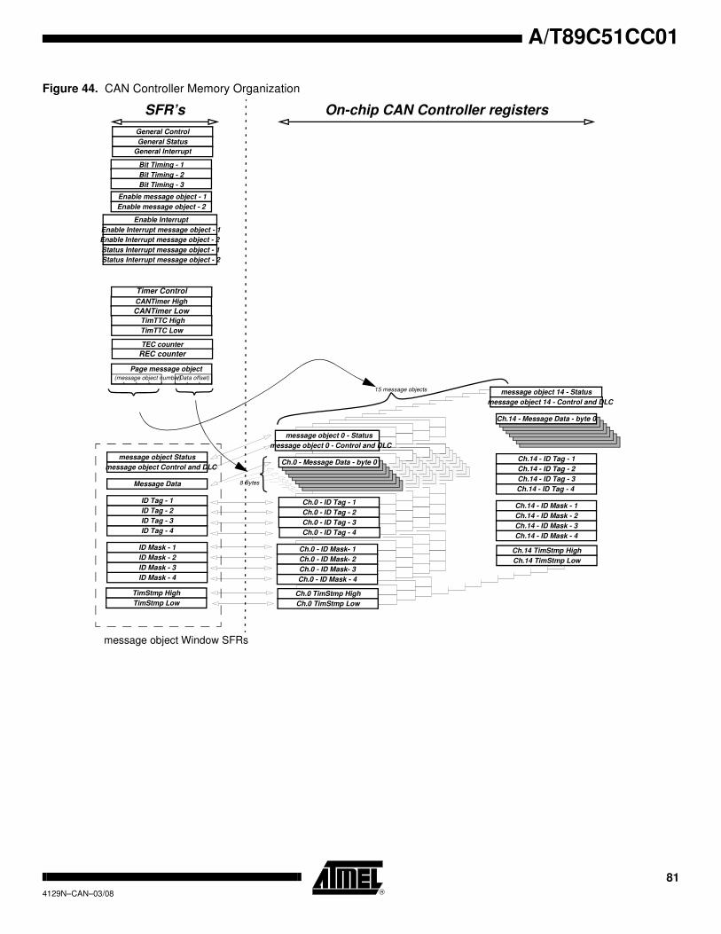
81
A/T89C51CC01
4129N–CAN–03/08
Figure 44. CAN Controller Memory Organization
Ch.14 - ID Tag - 1
Ch.14 - ID Tag - 2
Ch.14 - ID Tag - 4
Ch.14 - ID Tag - 3
Ch.14 - ID Mask - 1
Ch.14 - ID Mask - 2
Ch.14 - ID Mask - 4
Ch.14 - ID Mask - 3
Ch.14 - Message Data - byte 0
General Control
General Status
Bit Timing - 1
Bit Timing - 2
Bit Timing - 3
Enable Interrupt
Enable Interrupt message object - 1
Page message object
message object Status
message object Control and DLC
Message Data
ID Tag - 1
ID Tag - 2
ID Tag - 4
ID Tag - 3
ID Mask - 1
ID Mask - 2
ID Mask - 4
ID Mask - 3
message object 0 - Status
message object 0 - Control and DLC
Ch.0 - ID Tag - 1
Ch.0 - ID Tag - 2
Ch.0 - ID Tag - 4
Ch.0 - ID Tag - 3
Ch.0 - Message Data - byte 0
message object 14 - Status
message object 14 - Control and DLC
Enable Interrupt message object - 2
Status Interrupt message object - 1
Status Interrupt message object - 2
(message object number)(Data offset)
SFR’s On-chip CAN Controller registers
15 message objects
8 Bytes
TimStmp High
TimStmp Low
Ch.0 - ID Mask- 1
Ch.0 - ID Mask- 2
Ch.0 - ID Mask - 4
Ch.0 - ID Mask- 3
CANTimer High
CANTimer Low
TimTTC High
TimTTC Low
TEC counter
REC counter
Timer Control
Enable message object - 1
Enable message object - 2
message object Window SFRs
Ch.0 TimStmp High
Ch.0 TimStmp Low
Ch.14 TimStmp High
Ch.14 TimStmp Low
General Interrupt

82 A/T89C51CC014129N–CAN–03/08
Working on Message Objects The Page message object register (CANPAGE) is used to select one of the 15 message
objects. Then, message object Control (CANCONCH) and message object Status
(CANSTCH) are available for this selected message object number in the corresponding
SFRs. A single register (CANMSG) is used for the message. The mailbox pointer is
managed by the Page message object register with an auto-incrementation at the end of
each access. The range of this counter is 8.
Note that the maibox is a pure RAM, dedicated to one message object, without overlap.
In most cases, it is not necessary to transfer the received message into the standard
memory. The message to be transmitted can be built directly in the maibox. Most calcu-
lations or tests can be executed in the mailbox area which provide quicker access.
CAN Controller Management
In order to enable the CAN Controller correctly the following registers have to be
initialized:
• General Control (CANGCON),
• Bit Timing (CANBT 1, 2 and 3),
• And for each page of 15 message objects
– message object Control (CANCONCH),
– message object Status (CANSTCH).
During operation, the CAN Enable message object registers 1 and 2 (CANEN 1 and 2)
gives a fast overview of the message objects availability.
The CAN messages can be handled by interrupt or polling modes.
A message object can be configured as follows:
• Transmit message object,
• Receive message object,
• Receive buffer message object.
• Disable
This configuration is made in the CONCH field of the CANCONCH register (see
Table 56).
When a message object is configured, the corresponding ENCH bit of CANEN 1 and 2
register is set.
Table 56. Configuration for CONCH1:2
When a Transmitter or Receiver action of a message object is completed, the corre-
sponding ENCH bit of the CANEN 1 and 2 register is cleared. In order to re-enable the
message object, it is necessary to re-write the configuration in CANCONCH register.
Non-consecutive message objects can be used for all three types of message objects
(Transmitter, Receiver and Receiver buffer),
CONCH 1 CONCH 2 Type of Message Object
0 0 disable
0 1 Transmitter
1 0 Receiver
1 1 Receiver buffer

83
A/T89C51CC01
4129N–CAN–03/08
Buffer Mode Any message object can be used to define one buffer, including non-consecutive mes-
sage objects, and with no limitation in number of message objects used up to 15.
Each message object of the buffer must be initialized CONCH2 = 1 and CONCH1 = 1;
Figure 45. Buffer mode
The same acceptance filter must be defined for each message objects of the buffer.
When there is no mask on the identifier or the IDE, all messages are accepted.
A received frame will always be stored in the lowest free message object.
When the flag Rxok is set on one of the buffer message objects, this message object
can then be read by the application. This flag must then be cleared by the software and
the message object re-enabled in buffer reception in order to free the message object.
The OVRBUF flag in the CANGIT register is set when the buffer is full. This flag can
generate an interrupt.
The frames following the buffer-full interrupt will not stored and no status will be over-
written in the CANSTCH registers involved in the buffer until at least one of the buffer
message objects is re-enabled in reception.
This flag must be cleared by the software in order to acknowledge the interrupt.
message object 0
message object 1
message object 2
message object 3
message object 4
message object 5
message object 6
message object 7
message object 8
message object 9
message object 10
message object 11
message object 12
message object 13
Block buffer
buffer 0
buffer 1
buffer 2
buffer 3
buffer 4
buffer 5
buffer 6
buffer 7
message object 14
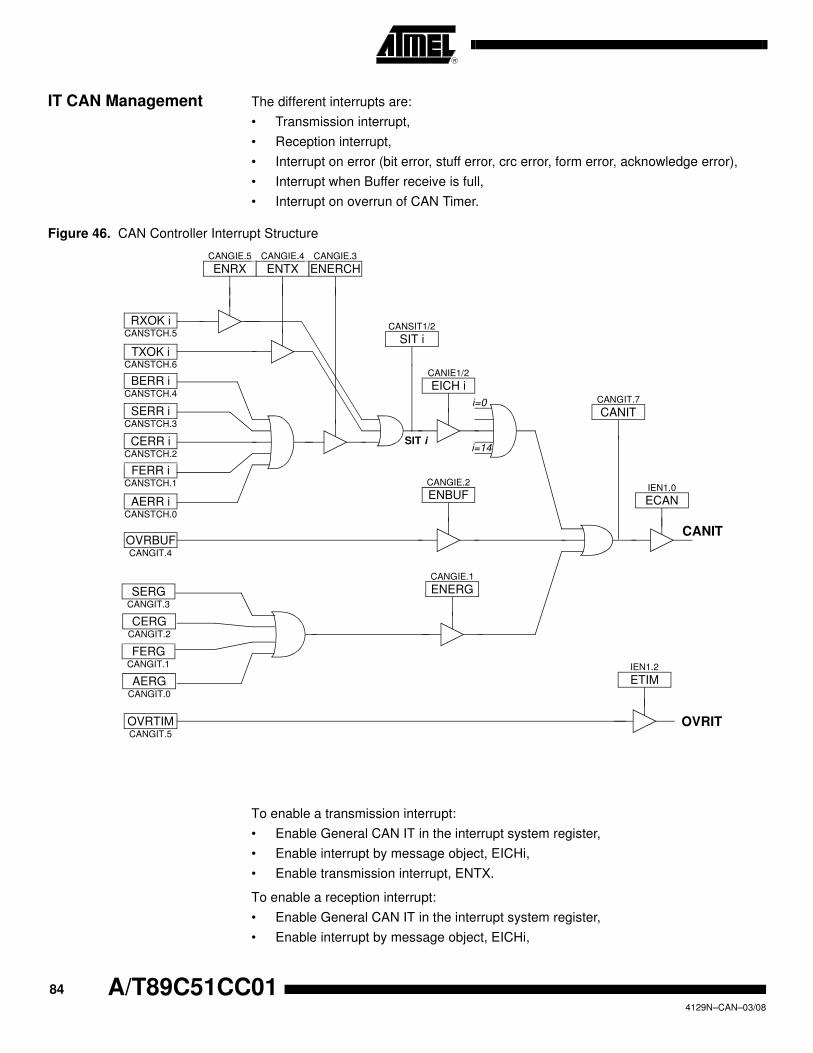
84 A/T89C51CC014129N–CAN–03/08
IT CAN Management The different interrupts are:
• Transmission interrupt,
• Reception interrupt,
• Interrupt on error (bit error, stuff error, crc error, form error, acknowledge error),
• Interrupt when Buffer receive is full,
• Interrupt on overrun of CAN Timer.
Figure 46. CAN Controller Interrupt Structure
To enable a transmission interrupt:
• Enable General CAN IT in the interrupt system register,
• Enable interrupt by message object, EICHi,
• Enable transmission interrupt, ENTX.
To enable a reception interrupt:
• Enable General CAN IT in the interrupt system register,
• Enable interrupt by message object, EICHi,
SIT i
i=0
i=14
OVRIT
ENRXCANGIE.5
ENTXCANGIE.4
ENERCHCANGIE.3
ENBUFCANGIE.2
ECANIEN1.0
RXOK iCANSTCH.5
TXOK iCANSTCH.6
BERR iCANSTCH.4
SERR iCANSTCH.3
FERR iCANSTCH.1
CERR iCANSTCH.2
AERR iCANSTCH.0
EICH iCANIE1/2
OVRTIMCANGIT.5
OVRBUFCANGIT.4
FERGCANGIT.1
AERGCANGIT.0
SERGCANGIT.3
CERGCANGIT.2
ENERGCANGIE.1
ETIMIEN1.2
SIT iCANSIT1/2
CANIT
CANITCANGIT.7

85
A/T89C51CC01
4129N–CAN–03/08
• Enable reception interrupt, ENRX.
To enable an interrupt on message object error:
• Enable General CAN IT in the interrupt system register,
• Enable interrupt by message object, EICHi,
• Enable interrupt on error, ENERCH.
To enable an interrupt on general error:
• Enable General CAN IT in the interrupt system register,
• Enable interrupt on error, ENERG.
To enable an interrupt on Buffer-full condition:
• Enable General CAN IT in the interrupt system register,
• Enable interrupt on Buffer full, ENBUF.
To enable an interrupt when Timer overruns:
• Enable Overrun IT in the interrupt system register.
When an interrupt occurs, the corresponding message object bit is set in the SIT
register.
To acknowledge an interrupt, the corresponding CANSTCH bits (RXOK, TXOK,...) or
CANGIT bits (OVRTIM, OVRBUF,...), must be cleared by the software application.
When the CAN node is in transmission and detects a Form Error in its frame, a bit Error
will also be raised. Consequently, two consecutive interrupts can occur, both due to the
same error.
When a message object error occurs and is set in CANSTCH register, no general error
are set in CANGIE register.

86 A/T89C51CC014129N–CAN–03/08
Bit Timing and Baud Rate
FSM’s (Finite State Machine) of the CAN channel need to be synchronous to the time
quantum. So, the input clock for bit timing is the clock used into CAN channel FSM’s.
Field and segment abbreviations:
• BRP: Baud Rate Prescaler.
• TQ: Time Quantum (output of Baud Rate Prescaler).
• SYNS: SYNchronization Segment is 1 TQ long.
• PRS: PRopagation time Segment is programmable to be 1, 2, ..., 8 TQ long.
• PHS1: PHase Segment 1 is programmable to be 1, 2, ..., 8 TQ long.
• PHS2: PHase Segment 2 is programmable to be superior or equal to the
INFORMATION PROCESSING TIME and inferior or equal to TPHS1.
• INFORMATION PROCESSING TIME is 2 TQ.
• SJW: (Re) Synchronization Jump Width is programmable to be minimum of PHS1
and 4.
The total number of TQ in a bit time has to be programmed at least from 8 to 25.
Figure 47. Sample And Transmission Point
The baud rate selection is made by Tbit calculation:
Tbit = Tsyns + Tprs + Tphs1 + Tphs2
1. Tsyns = Tscl = (BRP[5..0]+ 1)/Fcan = 1TQ.
2. Tprs = (1 to 8) * Tscl = (PRS[2..0]+ 1) * Tscl
3. Tphs1 = (1 to 8) * Tscl = (PHS1[2..0]+ 1) * Tscl
4. Tphs2 = (1 to 8) * Tscl = (PHS2[2..0]+ 1) * Tscl
Tphs2 = Max of (Tphs1 and 2TQ)
5. Tsjw = (1 to 4) * Tscl = (SJW[1..0]+ 1) * Tscl
The total number of Tscl (Time Quanta) in a bit time must be comprised between 8 to
25.
FCANCLOCK
Prescaler BRP
PRS 3-bit length
PHS1 3-bit length
PHS2 3-bit length
SJW 2-bit length
Bit Timing
System clock Tscl
Time Quantum
Sample point
Transmission point

87
A/T89C51CC01
4129N–CAN–03/08
Figure 48. General Structure of a Bit Period
example of bit timing determination for CAN baudrate of 500kbit/s:
Fosc = 12 MHz in X1 mode => FCAN = 6 MHz
Verify that the CAN baud rate you want is an integer division of FCAN clock.
FCAN/CAN baudrate = 6 MHz/500 kHz = 12
The time quanta TQ must be comprised between 8 and 25: TQ = 12 and BRP = 0
Define the various timing parameters: Tbit = Tsyns + Tprs + Tphs1 + Tphs2 =
12TQ
Tsyns = 1TQ and Tsjw =1TQ => SJW = 0
If we chose a sample point at 66.6% => Tphs2 = 4TQ => PHS2 = 3
Tbit = 12 = 4 + 1 + Tphs1 + Tprs, let us choose Tprs = 3 Tphs1 = 4
PHS1 = 3 and PRS = 2
BRP = 0 so CANBT1 = 00h
SJW = 0 and PRS = 2 so CANBT2 = 04h
PHS2 = 3 and PHS1 = 3 so CANBT3 = 36h
Bit Rate Prescaler
oscillator
1/ Fcan
Tscl
system clock
one nominal bit
Tsyns (*) Tprs
Sample Point(*) Synchronization Segment: SYNS
Tbit
Tsyns = 1xTscl (fixed)
data
Tbit Tsyns Tprs Tphs1 Tphs2+ + +=Tbit calculation:
Transmission Point
Tphs1 + Tsjw (3)Tphs2 - Tsjw (4)
(1) Phase error ≤ 0
(2) Phase error ≥ 0
(3) Phase error > 0(4) Phase error < 0
Tphs2 (2)Tphs1 (1)

88 A/T89C51CC014129N–CAN–03/08
Fault Confinement With respect to fault confinement, a unit may be in one of the three following status:
• error active
• error passive
• bus off
An error active unit takes part in bus communication and can send an active error frame
when the CAN macro detects an error.
An error passive unit cannot send an active error frame. It takes part in bus communica-
tion, but when an error is detected, a passive error frame is sent. Also, after a
transmission, an error passive unit will wait before initiating further transmission.
A bus off unit is not allowed to have any influence on the bus.
For fault confinement, two error counters (TEC and REC) are implemented.
See CAN Specification for details on Fault confinement.
Figure 49. Line Error Mode
TEC>255
ErrorActive
ErrorPassive
BusOff
Init.
TEC<127and
REC<127
TEC>127or
REC>127 128 Occurrencesof
11 ConsecutiveRecessive
bit
TEC: Transmit Error CounterREC: Receive Error Counter
ERRP = 0BOFF = 0
ERRP = 1BOFF = 0
ERRP = 0BOFF = 1

89
A/T89C51CC01
4129N–CAN–03/08
Acceptance Filter Upon a reception hit (i.e., a good comparison between the ID+RTR+RB+IDE received
and an ID+RTR+RB+IDE specified while taking the comparison mask into account) the
ID+RTR+RB+IDE received are written over the ID TAG Registers.
ID => IDT0-29
RTR => RTRTAG
RB => RB0-1TAG
IDE => IDE in CANCONCH register
Figure 50. Acceptance filter block diagram
example:
To accept only ID = 318h in part A.
ID MSK = 111 1111 1111 b
ID TAG = 011 0001 1000 b
13/32
=
13/32
RxDC
13/32
Write
13/32
1
Hit
13/32
ID MSK Registers (Ch i)
ID and RB RTR IDE
Rx Shift Register (internal)
ID and RB RTR IDE
Enable
(Ch i)
ID TAG Registers (Ch i) and CanConch
ID and RB RTR IDE

90 A/T89C51CC014129N–CAN–03/08
Data and Remote Frame Description of the different steps for:
• Data Frame
• Remote Frame, With Automatic Reply,
• Remote Frame
u uu uu0 1 x 0 0
u uu uu
ENCH
RTR
RPLV
TXO
KRXO
K
0 1 x 0 0
c uc uu0 0 x 1 0
u cc uu0 0 x 0 1
DATA FRAME
Node A Node B
ENCH
RTR
RPLV
TXO
KRXO
K
message object in reception
message object disabled
message object in
message object disabled
transmission
u uu uu1 1 x 0 0
c uu uc0 1 x 1 0
u cc uu0 0 x 0 1
REMOTE FRAME
DATA FRAME
u uu uu1 1 1 0 0
u uu cc0 1 0 0 0
c uc cu0 0 0 1 0
ENCH
RTR
RPLV
TXO
KRXO
K
ENCH
RTR
RPLV
TXO
KRXO
K
(immediate)
message object in reception
message object in transmission
message object disabled
message object in
message object in
message object disabled
by CAN controller by CAN controller
transmission
reception
u uu uu1 1 x 0 0
u uu uu
ENC
H
RTR
RPLV
TXO
KR
XO
K
1 1 0 0 0
c uu uc0 1 x 1 0
u cc uu1 0 0 0 1
REMOTE FRAME
ENC
H
RTR
RPLV
TXO
KR
XO
K
u uu uu0 1 x 0 0
c uc uu0 0 x 1 0
u cc uc0 0 x 0 1 DATA FRAME
(deferred)
u : modified by useri
c : modified by CANi
message object in reception
message object in transmission by user
message object disabled
message object disabled
message object in
message object in
message object disabled
reception by user
transmission

91
A/T89C51CC01
4129N–CAN–03/08
Time Trigger Communication (TTC) and Message Stamping
The T89C51CC01 has a programmable 16-bit Timer (CANTIMH and CANTIML) for
message stamp and TTC.
This CAN Timer starts after the CAN controller is enabled by the ENA bit in the CANG-
CON register.
Two modes in the timer are implemented:
• Time Trigger Communication:
– Capture of this timer value in the CANTTCH and CANTTCL registers on
Start Of Frame (SOF) or End Of Frame (EOF), depending on the SYNCTTC
bit in the CANGCON register, when the network is configured in TTC by the
TTC bit in the CANGCON register.
Note: In this mode, CAN only sends the frame once, even if an error occurs.
• Message Stamping
– Capture of this timer value in the CANSTMPH and CANSTMPL registers of
the message object which received or sent the frame.
– All messages can be stamps.
– The stamping of a received frame occurs when the RxOk flag is set.
– The stamping of a sent frame occurs when the TxOk flag is set.
The CAN Timer works in a roll-over from FFFFh to 0000h which serves as a time base.
When the timer roll-over from FFFFh to 0000h, an interrupt is generated if the ETIM bit
in the interrupt enable register IEN1 is set.
Figure 51. Block Diagram of CAN Timer
EOF on CAN frame
ENACANGCON.1
CANTCON
RXOK iCANSTCH.5
TXOK iCANSTCH.4
÷ 6Fcan
CLOCK
SOF on CAN frame
TTC
CANGCON.5
SYNCTTC
CANGCON.4
CANTTCH and CANTTCLCANSTMPH and CANSTMPL
CANTIMH and CANTIML
OVRTIMCANGIT.5
When 0xFFFF to 0x0000

92 A/T89C51CC014129N–CAN–03/08
CAN Autobaud and Listening Mode
To activate the Autobaud feature, the AUTOBAUD bit in the CANGCON register must
be set. In this mode, the CAN controller is only listening to the line without acknowledg-
ing the received messages. It cannot send any message. The error flags are updated.
The bit timing can be adjusted until no error occurs (good configuration find).
In this mode, the error counters are frozen.
To go back to the standard mode, the AUTOBAUD bit must be cleared.
Figure 52. Autobaud Mode
Routines Examples 1. Init of CAN macro
// Reset the CAN macro
CANGCON = 01h;
// Disable CAN interrupts
ECAN = 0;
ETIM = 0;
// Init the Mailbox
for num_page =0; num_page <15; num_page++
CANPAGE = num_channel << 4;
CANCONCH = 00h
CANSTCH = 00h;
CANIDT1 = 00h;
CANIDT2 = 00h;
CANIDT3 = 00h;
CANIDT4 = 00h;
CANIDM1 = 00h;
CANIDM2 = 00h;
CANIDM3 = 00h;
CANIDM4 = 00h;
for num_data =0; num_data <8; num_data++)
CANMSG = 00h;
// Configure the bit timing
CANBT1 = xxh
CANBT2 = xxh
CANBT3 = xxh
0
1
TxDC
RxDC’
AUTOBAUD
CANGCON.3 RxDC
TxDC’

93
A/T89C51CC01
4129N–CAN–03/08
// Enable the CAN macro
CANGCON = 02h
2. Configure message object 3 in reception to receive only standard (11-bit identi-
fier) message 100h
// Select the message object 3
CANPAGE = 30h
// Enable the interrupt on this message object
CANIE2 = 08h
// Clear the status and control register
CANSTCH = 00h
CANCONCH = 00h
// Init the acceptance filter to accept only message 100h in standard mode
CANIDT1 = 20h
CANIDT2 = 00h
CANIDT3 = 00h
CANIDT4 = 00h
CANIDM1 = FFh
CANIDM2 = FFh
CANIDM3 = FFh
CANIDM4 = FFh
// Enable channel in reception
CANCONCH = 88h // enable reception
Note: To enable the CAN interrupt in reception:
EA = 1
ECAN = 1
CANGIE = 20h
3. Send a message on the message object 12
// Select the message object 12
CANPAGE = C0h
// Enable the interrupt on this message object
CANIE1 = 01h
// Clear the Status register
CANSTCH = 00h;
// load the identifier to send (ex: 555h)
CANIDT1 = AAh;
CANIDT2 = A0h;
// load data to send
CANMSG = 00h
CANMSG = 01h
CANMSG = 02h
CANMSG = 03h
CANMSG = 04h
CANMSG = 05h
CANMSG = 06h
CANMSG = 07h
// configure the control register
CANCONCH = 18h
94 A/T89C51CC014129N–CAN–03/08
4. Interrupt routine
// Save the current CANPAGE
// Find the first message object which generate an interrupt in CANSIT1 and
CANSIT2
// Select the corresponding message object
// Analyse the CANSTCH register to identify which kind of interrupt is
generated
// Manage the interrupt
// Clear the status register CANSTCH = 00h;
// if it is not a channel interrupt but a general interrupt
// Manage the general interrupt and clear CANGIT register
// restore the old CANPAGE

95
A/T89C51CC01
4129N–CAN–03/08
CAN SFR’s
Table 57. CAN SFR’s With Reset Values
0/8(1) 1/9 2/A 3/B 4/C 5/D 6/E 7/F
F8hIPL1
xxxx x000
CH
0000 0000
CCAP0H
0000 0000
CCAP1H
0000 0000
CCAP2H
0000 0000
CCAP3H
0000 0000
CCAP4H
0000 0000FFh
F0hB
0000 0000
ADCLK
xxx0 0000
ADCON
x000 0000
ADDL
0000 0000
ADDH
0000 0000
ADCF
0000 0000
IPH1
xxxx x000F7h
E8hIEN1
xxxx x000
CL
0000 0000
CCAP0L
0000 0000
CCAP1L
0000 0000
CCAP2L
0000 0000
CCAP3L
0000 0000
CCAP4L
0000 0000EFh
E0hACC
0000 0000E7h
D8hCCON
00x0 0000
CMOD
00xx x000
CCAPM0
x000 0000
CCAPM1
x000 0000
CCAPM2
x000 0000
CCAPM3
x000 0000
CCAPM4
x000 0000DFh
D0hPSW
0000 0000
FCON
0000 0000
EECON
xxxx xx00D7h
C8hT2CON
0000 0000
T2MOD
xxxx xx00
RCAP2L
0000 0000
RCAP2H
0000 0000
TL2
0000 0000
TH2
0000 0000
CANEN1
x000 0000
CANEN2
0000 0000CFh
C0hP4
xxxx xx11
CANGIE
1100 0000
CANIE1
x000 0000
CANIE2
0000 0000
CANIDM1
xxxx xxxx
CANIDM2
xxxx xxxx
CANIDM3
xxxx xxxx
CANIDM4
xxxx xxxxC7h
B8hIPL0
x000 0000
SADEN
0000 0000
CANSIT1
x000 0000
CANSIT2
0000 0000
CANIDT1
xxxx xxxx
CANIDT2
xxxx xxxx
CANIDT3
xxxx xxxx
CANIDT4
xxxx xxxxBFh
B0hP3
1111 1111
CANPAGE
0000 0000
CANSTCH
xxxx xxxx
CANCONCH
xxxx xxxx
CANBT1
xxxx xxxx
CANBT2
xxxx xxxx
CANBT3
xxxx xxxx
IPH0
x000 0000B7h
A8hIEN0
0000 0000
SADDR
0000 0000
CANGSTA
1010 0000
CANGCON
0000 0000
CANTIML
0000 0000
CANTIMH
0000 0000
CANSTMPL
xxxx xxxx
CANSTMPH
xxxx xxxxAFh
A0hP2
1111 1111
CANTCON
0000 0000
AUXR1
xxxx 00x0
CANMSG
xxxx xxxx
CANTTCL
0000 0000
CANTTCH
0000 0000
WDTRST
1111 1111
WDTPRG
xxxx x000A7h
98hSCON
0000 0000
SBUF
0000 0000
CANGIT
0x00 0000
CANTEC
0000 0000
CANREC
0000 00009Fh
90hP1
1111 111197h
88hTCON
0000 0000
TMOD
0000 0000
TL0
0000 0000
TL1
0000 0000
TH0
0000 0000
TH1
0000 0000
AUXR
x00x 1100
CKCON
0000 00008Fh
80hP0
1111 1111
SP
0000 0111
DPL
0000 0000
DPH
0000 0000
PCON
00x1 000087h
0/8(1) 1/9 2/A 3/B 4/C 5/D 6/E 7/F
96 A/T89C51CC014129N–CAN–03/08
Registers Table 58. CANGCON Register
CANGCON (S:ABh)
CAN General Control Register
Reset Value = 0000 0000b
7 6 5 4 3 2 1 0
ABRQ OVRQ TTC SYNCTTC AUTOBAUD TEST ENA GRES
Bit
Number Bit Mnemonic Description
7 ABRQ
Abort Request
Not an auto-resetable bit. A reset of the ENCH bit (message object control
and DLC register) is done for each message object. The pending transmission
communications are immediately aborted but the on-going communication will
be terminated normally, setting the appropriate status flags, TXOK or RXOK.
6 OVRQ
Overload frame request (initiator)
Auto-resetable bit.
Set to send an overload frame after the next received message.
Cleared by the hardware at the beginning of transmission of the overload
frame.
5 TTC
Network in Timer Trigger Communication
set to select node in TTC.
clear to disable TTC features.
4 SYNCTTC
Synchronization of TTC
When this bit is set the TTC timer is caught on the last bit of the End Of
Frame.
When this bit is clear the TTC timer is caught on the Start Of Frame.
This bit is only used in the TTC mode.
3 AUTOBAUD
AUTOBAUD
set to active listening mode.
Clear to disable listening mode
2 TESTTest mode. The test mode is intended for factory testing and not for customer
use.
1 ENA/STB
Enable/Standby CAN Controller
When this bit is set, it enables the CAN controller and its input clock.
When this bit is clear, the on-going communication is terminated normally and
the CAN controller state of the machine is frozen (the ENCH bit of each
message object does not change).
In the standby mode, the transmitter constantly provides a recessive level; the
receiver is not activated and the input clock is stopped in the CAN controller.
During the disable mode, the registers and the mailbox remain accessible.
Note that two clock periods are needed to start the CAN controller state of the
machine.
0 GRES
General Reset (software reset)
Auto-resetable bit. This reset command is ‘ORed’ with the hardware reset in
order to reset the controller. After a reset, the controller is disabled.
97
A/T89C51CC01
4129N–CAN–03/08
Table 59. CANGSTA Register
CANGSTA (S:AAh Read Only)
CAN General Status Register
Reset Value = x0x0 0000b
7 6 5 4 3 2 1 0
- OVFG - TBSY RBSY ENFG BOFF ERRP
Bit
Number Bit Mnemonic Description
7 -Reserved
The values read from this bit is indeterminate. Do not set this bit.
6 OVFG
Overload Frame Flag
This status bit is set by the hardware as long as the produced overload frame
is sent.
This flag does not generate an interrupt
5 -Reserved
The values read from this bit is indeterminate. Do not set this bit.
4 TBSY
Transmitter Busy
This status bit is set by the hardware as long as the CAN transmitter
generates a frame (remote, data, overload or error frame) or an ack field. This
bit is also active during an InterFrame Spacing if a frame must be sent.
This flag does not generate an interrupt.
3 RBSY
Receiver Busy
This status bit is set by the hardware as long as the CAN receiver acquires or
monitors a frame.
This flag does not generate an interrupt.
2 ENFG
Enable On-chip CAN Controller Flag
Because an enable/disable command is not effective immediately, this status
bit gives the true state of a chosen mode.
This flag does not generate an interrupt.
1 BOFFBus Off Mode
see Figure 49
0 ERRPError Passive Mode
see Figure 49

98 A/T89C51CC014129N–CAN–03/08
Table 60. CANGIT Register
CANGIT (S:9Bh)
CAN General Interrupt
Note: 1. This field is Read Only.
Reset Value = 0x00 0000b
7 6 5 4 3 2 1 0
CANIT - OVRTIM OVRBUF SERG CERG FERG AERG
Bit
Number Bit Mnemonic Description
7 CANIT
General Interrupt Flag(1)
This status bit is the image of all the CAN controller interrupts sent to the
interrupt controller.
It can be used in the case of the polling method.
6 -Reserved
The values read from this bit is indeterminate. Do not set this bit.
5 OVRTIM
Overrun CAN Timer
This status bit is set when the CAN timer switches 0xFFFF to 0x0000.
If the bit ETIM in the IE1 register is set, an interrupt is generated.
Clear this bit in order to reset the interrupt.
4 OVRBUF
Overrun BUFFER
0 - no interrupt.
1 - IT turned on
This bit is set when the buffer is full.
Bit resetable by user.
see Figure 46.
3 SERG
Stuff Error General
Detection of more than five consecutive bits with the same polarity.
This flag can generate an interrupt. resetable by user.
2 CERG
CRC Error General
The receiver performs a CRC check on each destuffed received message
from the start of frame up to the data field.
If this checking does not match with the destuffed CRC field, a CRC error is
set.
This flag can generate an interrupt. resetable by user.
1 FERG
Form Error General
The form error results from one or more violations of the fixed form in the
following bit fields:
CRC delimiter
acknowledgment delimiter
end_of_frame
This flag can generate an interrupt. resetable by user.
0 AERG
Acknowledgment Error General
No detection of the dominant bit in the acknowledge slot.
This flag can generate an interrupt. resetable by user.

99
A/T89C51CC01
4129N–CAN–03/08
Table 61. CANTEC Register
CANTEC (S:9Ch Read Only)
CAN Transmit Error Counter
Reset Value = 00h
Table 62. CANREC Register
CANREC (S:9Dh Read Only)
CAN Reception Error Counter
Reset Value = 00h
7 6 5 4 3 2 1 0
TEC7 TEC6 TEC5 TEC4 TEC3 TEC2 TEC1 TEC0
Bit
Number Bit Mnemonic Description
7-0 TEC7:0Transmit Error Counter
see Figure 49
7 6 5 4 3 2 1 0
REC7 REC6 REC5 REC4 REC3 REC2 REC1 REC0
Bit
Number Bit Mnemonic Description
7-0 REC7:0Reception Error Counter
see Figure 49

100 A/T89C51CC014129N–CAN–03/08
Table 63. CANGIE Register
CANGIE (S:C1h)
CAN General Interrupt Enable
Note: See Figure 46
Reset Value = xx00 000xb
Table 64. CANEN1 Register
CANEN1 (S:CEh Read Only)
CAN Enable Message Object Registers 1
Reset Value = x000 0000b
7 6 5 4 3 2 1 0
- - ENRX ENTX ENERCH ENBUF ENERG -
Bit
Number Bit Mnemonic Description
7-6 -Reserved
The values read from these bits are indeterminate. Do not set these bits.
5 ENRX
Enable Receive Interrupt
0 - Disable
1 - Enable
4 ENTX
Enable Transmit Interrupt
0 - Disable
1 - Enable
3 ENERCH
Enable Message Object Error Interrupt
0 - Disable
1 - Enable
2 ENBUF
Enable BUF Interrupt
0 - Disable
1 - Enable
1 ENERG
Enable General Error Interrupt
0 - Disable
1 - Enable
0 -Reserved
The value read from this bit is indeterminate. Do not set this bit.
7 6 5 4 3 2 1 0
- ENCH14 ENCH13 ENCH12 ENCH11 ENCH10 ENCH9 ENCH8
Bit
Number Bit Mnemonic Description
7 -Reserved
The values read from this bit is indeterminate. Do not set this bit.
6-0 ENCH14:8
Enable Message Object
0 - message object is disabled => the message object is free for a new
emission or reception.
1 - message object is enabled.
This bit is resetable by re-writing the CANCONCH of the corresponding
message object.

101
A/T89C51CC01
4129N–CAN–03/08
Table 65. CANEN2 Register
CANEN2 (S:CFh Read Only)
CAN Enable Message Object Registers 2
Reset Value = 0000 0000b
Table 66. CANSIT1 Register
CANSIT1 (S:BAh Read Only)
CAN Status Interrupt Message Object Registers 1
Reset Value = x000 0000b
7 6 5 4 3 2 1 0
ENCH7 ENCH6 ENCH5 ENCH4 ENCH3 ENCH2 ENCH1 ENCH0
Bit
Number Bit Mnemonic Description
7-0 ENCH7:0
Enable Message Object
0 - message object is disabled => the message object is free for a new
emission or reception.
1 - message object is enabled.
This bit is resetable by re-writing the CANCONCH of the corresponding
message object.
7 6 5 4 3 2 1 0
- SIT14 SIT13 SIT12 SIT11 SIT10 SIT9 SIT8
Bit
Number Bit Mnemonic Description
7 -Reserved
The values read from this bit is indeterminate. Do not set this bit.
6-0 SIT14:8
Status of Interrupt by Message Object
0 - no interrupt.
1 - IT turned on. Reset when interrupt condition is cleared by user.
SIT14:8 = 0b 0000 1001 -> IT’s on message objects 11 and 8.
see Figure 46.
102 A/T89C51CC014129N–CAN–03/08
Table 67. CANSIT2 Register
CANSIT2 (S:BBh Read Only)
CAN Status Interrupt Message Object Registers 2
Reset Value = 0000 0000b
Table 68. CANIE1 Register
CANIE1 (S:C2h)
CAN Enable Interrupt Message Object Registers 1
Reset Value = x000 0000b
7 6 5 4 3 2 1 0
SIT7 SIT6 SIT5 SIT4 SIT3 SIT2 SIT1 SIT0
Bit
Number Bit Mnemonic Description
7-0 SIT7:0
Status of Interrupt by Message Object
0 - no interrupt.
1 - IT turned on. Reset when interrupt condition is cleared by user.
SIT7:0 = 0b 0000 1001 -> IT’s on message objects 3 and 0
see Figure 46.
7 6 5 4 3 2 1 0
- IECH14 IECH13 IECH12 IECH11 IECH10 IECH9 IECH8
Bit
Number Bit Mnemonic Description
7 -Reserved
The values read from this bit is indeterminate. Do not set this bit.
6-0 IECH14:8
Enable interrupt by Message Object
0 - disable IT.
1 - enable IT.
IECH14:8 = 0b 0000 1100 -> Enable IT’s of message objects 11 and 10.
see Figure 46.

103
A/T89C51CC01
4129N–CAN–03/08
Table 69. CANIE2 Register
CANIE2 (S:C3h)
CAN Enable Interrupt Message Object Registers 2
Reset Value = 0000 0000b
Table 70. CANBT1 Register
CANBT1 (S:B4h)
CAN Bit Timing Registers 1
Note: The CAN controller bit timing registers must be accessed only if the CAN controller is dis-
abled with the ENA bit of the CANGCON register set to 0.
See Figure 48.
No default value after reset.
7 6 5 4 3 2 1 0
IECH 7 IECH 6 IECH 5 IECH 4 IECH 3 IECH 2 IECH 1 IECH 0
Bit
Number Bit Mnemonic Description
7-0 IECH7:0
Enable interrupt by Message Object
0 - disable IT.
1 - enable IT.
IECH7:0 = 0b 0000 1100 -> Enable IT’s of message objects 3 and 2.
7 6 5 4 3 2 1 0
- BRP 5 BRP 4 BRP 3 BRP 2 BRP 1 BRP 0 -
Bit
Number Bit Mnemonic Description
7 -Reserved
The value read from this bit is indeterminate. Do not set this bit.
6-1 BRP5:0
Baud rate prescaler
The period of the CAN controller system clock Tscl is programmable and
determines the individual bit timing.
0 -Reserved
The value read from this bit is indeterminate. Do not set this bit.
Tscl =BRP[5..0] + 1
Fcan

104 A/T89C51CC014129N–CAN–03/08
Table 71. CANBT2 Register
CANBT2 (S:B5h)
CAN Bit Timing Registers 2
Note: The CAN controller bit timing registers must be accessed only if the CAN controller is dis-
abled with the ENA bit of the CANGCON register set to 0.
See Figure 48.
No default value after reset.
7 6 5 4 3 2 1 0
- SJW 1 SJW 0 - PRS 2 PRS 1 PRS 0 -
Bit
Number Bit Mnemonic Description
7 -Reserved
The value read from this bit is indeterminate. Do not set this bit.
6-5 SJW1:0
Re-synchronization Jump Width
To compensate for phase shifts between clock oscillators of different bus
controllers, the controller must re-synchronize on any relevant signal edge of
the current transmission.
The synchronization jump width defines the maximum number of clock cycles.
A bit period may be shortened or lengthened by a re-synchronization.
4 -Reserved
The value read from this bit is indeterminate. Do not set this bit.
3-1 PRS2:0
Programming Time Segment
This part of the bit time is used to compensate for the physical delay times
within the network. It is twice the sum of the signal propagation time on the
bus line, the input comparator delay and the output driver delay.
0 -Reserved
The value read from this bit is indeterminate. Do not set this bit.
Tsjw = Tscl x (SJW [1..0] +1)
Tprs = Tscl x (PRS[2..0] + 1)

105
A/T89C51CC01
4129N–CAN–03/08
Table 72. CANBT3 Register
CANBT3 (S:B6h)
CAN Bit Timing Registers 3
Note: The CAN controller bit timing registers must be accessed only if the CAN controller is dis-
abled with the ENA bit of the CANGCON register set to 0.
See Figure 48.
No default value after reset.
7 6 5 4 3 2 1 0
- PHS2 2 PHS2 1 PHS2 0 PHS1 2 PHS1 1 PHS1 0 SMP
Bit
Number Bit Mnemonic Description
7 -Reserved
The value read from this bit is indeterminate. Do not set this bit.
6-4 PHS2 2:0
Phase Segment 2
This phase is used to compensate for phase edge errors. This segment can
be shortened by the re-synchronization jump width.
Phase segment 2 is the maximum of Phase segment1 and the Information
Processing Time (= 2TQ).
3-1 PHS1 2:0
Phase Segment 1
This phase is used to compensate for phase edge errors. This segment can
be lengthened by the re-synchronization jump width.
0 SMP
Sample Type
0 - once, at the sample point.
1 - three times, the threefold sampling of the bus is the sample point and twice
over a distance of a 1/2 period of the Tscl. The result corresponds to the
majority decision of the three values.
Tphs2 = Tscl x (PHS2[2..0] + 1)
Tphs1 = Tscl x (PHS1[2..0] + 1)

106 A/T89C51CC014129N–CAN–03/08
Table 73. CANPAGE Register
CANPAGE (S:B1h)
CAN Message Object Page Register
Reset Value = 0000 0000b
Table 74. CANCONCH Register
CANCONCH (S:B3h)
CAN Message Object Control and DLC Register
No default value after reset
7 6 5 4 3 2 1 0
CHNB 3 CHNB 2 CHNB 1 CHNB 0 AINC INDX2 INDX1 INDX0
Bit
Number Bit Mnemonic Description
7-4 CHNB3:0Selection of Message Object Number
The available numbers are: 0 to 14 (see Figure 44).
3 AINC
Auto Increment of the Index (active low)
0 - auto-increment of the index (default value).
1 - non-auto-increment of the index.
2-0 INDX2:0Index
Byte location of the data field for the defined message object (see Figure 44).
7 6 5 4 3 2 1 0
CONCH 1 CONCH 0 RPLV IDE DLC 3 DLC 2 DLC 1 DLC 0
Bit
Number Bit Mnemonic Description
7-6 CONCH1:0
Configuration of Message Object
CONCH1 CONCH0
0 0: disable
0 1: Launch transmission
1 0: Enable Reception
1 1: Enable Reception Buffer
Note: The user must re-write the configuration to enable the corresponding bit
in the CANEN1:2 registers.
5 RPLV
Reply Valid
Used in the automatic reply mode after receiving a remote frame
0 - reply not ready.
1 - reply ready and valid.
4 IDE
Identifier Extension
0 - CAN standard rev 2.0 A (ident = 11 bits).
1 - CAN standard rev 2.0 B (ident = 29 bits).
3-0 DLC3:0
Data Length Code
Number of Bytes in the data field of the message.
The range of DLC is from 0 up to 8.
This value is updated when a frame is received (data or remote frame).
If the expected DLC differs from the incoming DLC, a warning appears in the
CANSTCH register.
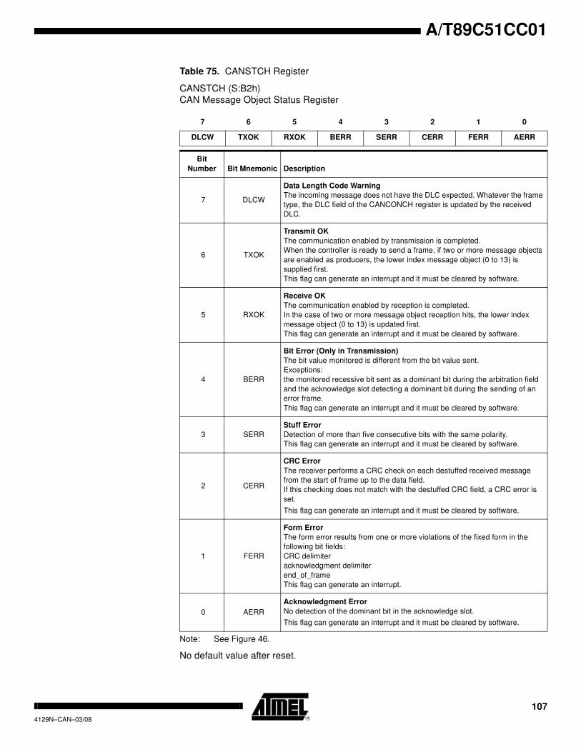
107
A/T89C51CC01
4129N–CAN–03/08
Table 75. CANSTCH Register
CANSTCH (S:B2h)
CAN Message Object Status Register
Note: See Figure 46.
No default value after reset.
7 6 5 4 3 2 1 0
DLCW TXOK RXOK BERR SERR CERR FERR AERR
Bit
Number Bit Mnemonic Description
7 DLCW
Data Length Code Warning
The incoming message does not have the DLC expected. Whatever the frame
type, the DLC field of the CANCONCH register is updated by the received
DLC.
6 TXOK
Transmit OK
The communication enabled by transmission is completed.
When the controller is ready to send a frame, if two or more message objects
are enabled as producers, the lower index message object (0 to 13) is
supplied first.
This flag can generate an interrupt and it must be cleared by software.
5 RXOK
Receive OK
The communication enabled by reception is completed.
In the case of two or more message object reception hits, the lower index
message object (0 to 13) is updated first.
This flag can generate an interrupt and it must be cleared by software.
4 BERR
Bit Error (Only in Transmission)
The bit value monitored is different from the bit value sent.
Exceptions:
the monitored recessive bit sent as a dominant bit during the arbitration field
and the acknowledge slot detecting a dominant bit during the sending of an
error frame.
This flag can generate an interrupt and it must be cleared by software.
3 SERR
Stuff Error
Detection of more than five consecutive bits with the same polarity.
This flag can generate an interrupt and it must be cleared by software.
2 CERR
CRC Error
The receiver performs a CRC check on each destuffed received message
from the start of frame up to the data field.
If this checking does not match with the destuffed CRC field, a CRC error is
set.
This flag can generate an interrupt and it must be cleared by software.
1 FERR
Form Error
The form error results from one or more violations of the fixed form in the
following bit fields:
CRC delimiter
acknowledgment delimiter
end_of_frame
This flag can generate an interrupt.
0 AERR
Acknowledgment Error
No detection of the dominant bit in the acknowledge slot.
This flag can generate an interrupt and it must be cleared by software.
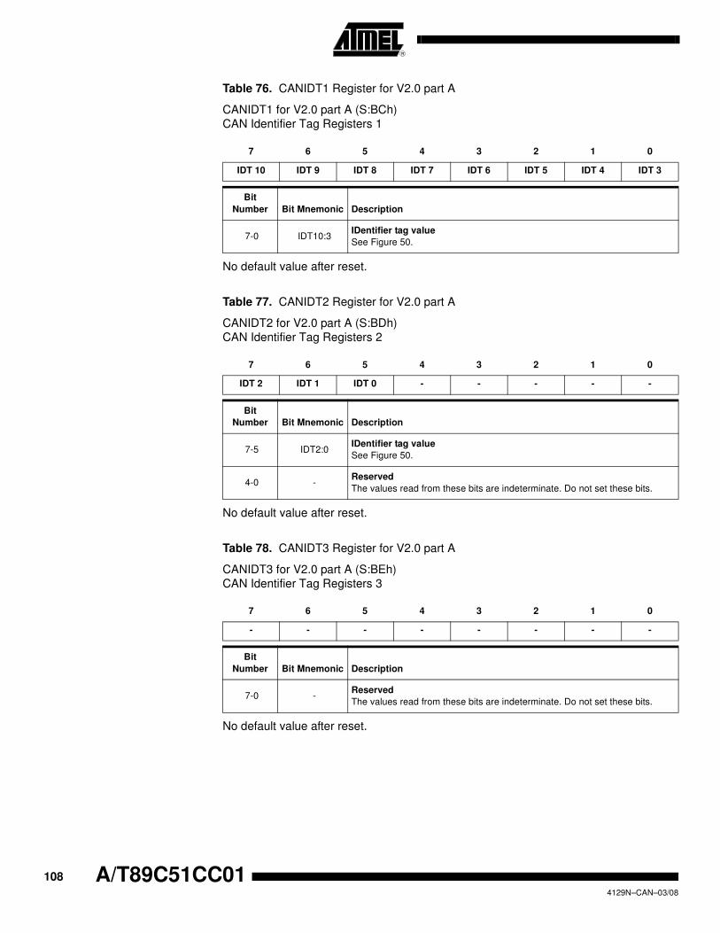
108 A/T89C51CC014129N–CAN–03/08
Table 76. CANIDT1 Register for V2.0 part A
CANIDT1 for V2.0 part A (S:BCh)
CAN Identifier Tag Registers 1
No default value after reset.
Table 77. CANIDT2 Register for V2.0 part A
CANIDT2 for V2.0 part A (S:BDh)
CAN Identifier Tag Registers 2
No default value after reset.
Table 78. CANIDT3 Register for V2.0 part A
CANIDT3 for V2.0 part A (S:BEh)
CAN Identifier Tag Registers 3
No default value after reset.
7 6 5 4 3 2 1 0
IDT 10 IDT 9 IDT 8 IDT 7 IDT 6 IDT 5 IDT 4 IDT 3
Bit
Number Bit Mnemonic Description
7-0 IDT10:3IDentifier tag value
See Figure 50.
7 6 5 4 3 2 1 0
IDT 2 IDT 1 IDT 0 - - - - -
Bit
Number Bit Mnemonic Description
7-5 IDT2:0IDentifier tag value
See Figure 50.
4-0 -Reserved
The values read from these bits are indeterminate. Do not set these bits.
7 6 5 4 3 2 1 0
- - - - - - - -
Bit
Number Bit Mnemonic Description
7-0 -Reserved
The values read from these bits are indeterminate. Do not set these bits.
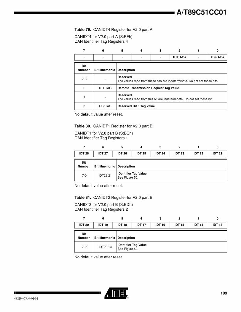
109
A/T89C51CC01
4129N–CAN–03/08
Table 79. CANIDT4 Register for V2.0 part A
CANIDT4 for V2.0 part A (S:BFh)
CAN Identifier Tag Registers 4
No default value after reset.
Table 80. CANIDT1 Register for V2.0 part B
CANIDT1 for V2.0 part B (S:BCh)
CAN Identifier Tag Registers 1
No default value after reset.
Table 81. CANIDT2 Register for V2.0 part B
CANIDT2 for V2.0 part B (S:BDh)
CAN Identifier Tag Registers 2
No default value after reset.
7 6 5 4 3 2 1 0
- - - - - RTRTAG - RB0TAG
Bit
Number Bit Mnemonic Description
7-3 -Reserved
The values read from these bits are indeterminate. Do not set these bits.
2 RTRTAG Remote Transmission Request Tag Value.
1 -Reserved
The values read from this bit are indeterminate. Do not set these bit.
0 RB0TAG Reserved Bit 0 Tag Value.
7 6 5 4 3 2 1 0
IDT 28 IDT 27 IDT 26 IDT 25 IDT 24 IDT 23 IDT 22 IDT 21
Bit
Number Bit Mnemonic Description
7-0 IDT28:21IDentifier Tag Value
See Figure 50.
7 6 5 4 3 2 1 0
IDT 20 IDT 19 IDT 18 IDT 17 IDT 16 IDT 15 IDT 14 IDT 13
Bit
Number Bit Mnemonic Description
7-0 IDT20:13IDentifier Tag Value
See Figure 50.

110 A/T89C51CC014129N–CAN–03/08
Table 82. CANIDT3 Register for V2.0 part B
CANIDT3 for V2.0 part B (S:BEh)
CAN Identifier Tag Registers 3
No default value after reset.
Table 83. CANIDT4 Register for V2.0 part B
CANIDT4 for V2.0 part B (S:BFh)
CAN Identifier Tag Registers 4
No default value after reset.
Table 84. CANIDM1 Register for V2.0 part A
CANIDM1 for V2.0 part A (S:C4h)
CAN Identifier Mask Registers 1
No default value after reset.
7 6 5 4 3 2 1 0
IDT 12 IDT 11 IDT 10 IDT 9 IDT 8 IDT 7 IDT 6 IDT 5
Bit
Number Bit Mnemonic Description
7-0 IDT12:5IDentifier Tag Value
See Figure 50.
7 6 5 4 3 2 1 0
IDT 4 IDT 3 IDT 2 IDT 1 IDT 0 RTRTAG RB1TAG RB0TAG
Bit
Number Bit Mnemonic Description
7-3 IDT4:0IDentifier Tag Value
See Figure 50.
2 RTRTAG Remote Transmission Request Tag Value
1 RB1TAG Reserved bit 1 Tag Value
0 RB0TAG Reserved bit 0 Tag Value
7 6 5 4 3 2 1 0
IDMSK 10 IDMSK 9 IDMSK 8 IDMSK 7 IDMSK 6 IDMSK 5 IDMSK 4 IDMSK 3
Bit
Number Bit Mnemonic Description
7-0 IDTMSK10:3
IDentifier mask value
0 - comparison true forced.
1 - bit comparison enabled.
See Figure 50.
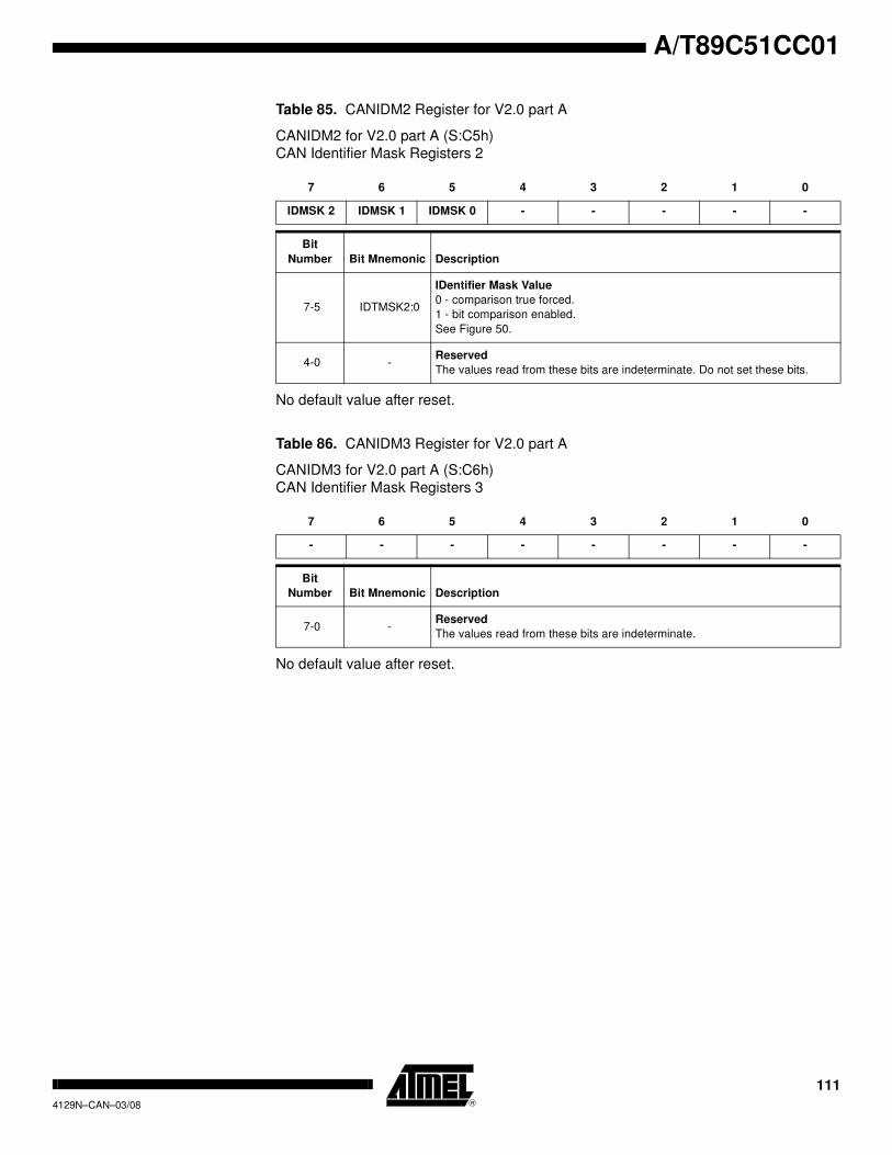
111
A/T89C51CC01
4129N–CAN–03/08
Table 85. CANIDM2 Register for V2.0 part A
CANIDM2 for V2.0 part A (S:C5h)
CAN Identifier Mask Registers 2
No default value after reset.
Table 86. CANIDM3 Register for V2.0 part A
CANIDM3 for V2.0 part A (S:C6h)
CAN Identifier Mask Registers 3
No default value after reset.
7 6 5 4 3 2 1 0
IDMSK 2 IDMSK 1 IDMSK 0 - - - - -
Bit
Number Bit Mnemonic Description
7-5 IDTMSK2:0
IDentifier Mask Value
0 - comparison true forced.
1 - bit comparison enabled.
See Figure 50.
4-0 -Reserved
The values read from these bits are indeterminate. Do not set these bits.
7 6 5 4 3 2 1 0
- - - - - - - -
Bit
Number Bit Mnemonic Description
7-0 -Reserved
The values read from these bits are indeterminate.
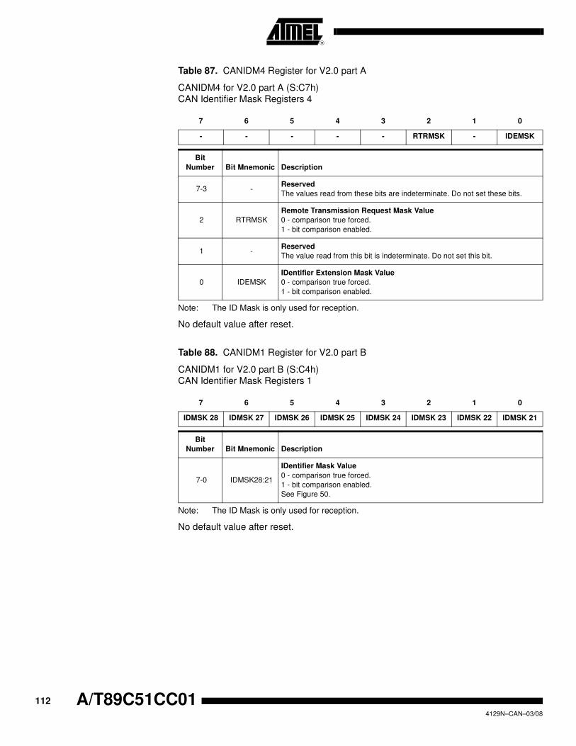
112 A/T89C51CC014129N–CAN–03/08
Table 87. CANIDM4 Register for V2.0 part A
CANIDM4 for V2.0 part A (S:C7h)
CAN Identifier Mask Registers 4
Note: The ID Mask is only used for reception.
No default value after reset.
Table 88. CANIDM1 Register for V2.0 part B
CANIDM1 for V2.0 part B (S:C4h)
CAN Identifier Mask Registers 1
Note: The ID Mask is only used for reception.
No default value after reset.
7 6 5 4 3 2 1 0
- - - - - RTRMSK - IDEMSK
Bit
Number Bit Mnemonic Description
7-3 -Reserved
The values read from these bits are indeterminate. Do not set these bits.
2 RTRMSK
Remote Transmission Request Mask Value
0 - comparison true forced.
1 - bit comparison enabled.
1 -Reserved
The value read from this bit is indeterminate. Do not set this bit.
0 IDEMSK
IDentifier Extension Mask Value
0 - comparison true forced.
1 - bit comparison enabled.
7 6 5 4 3 2 1 0
IDMSK 28 IDMSK 27 IDMSK 26 IDMSK 25 IDMSK 24 IDMSK 23 IDMSK 22 IDMSK 21
Bit
Number Bit Mnemonic Description
7-0 IDMSK28:21
IDentifier Mask Value
0 - comparison true forced.
1 - bit comparison enabled.
See Figure 50.

113
A/T89C51CC01
4129N–CAN–03/08
Table 89. CANIDM2 Register for V2.0 part B
CANIDM2 for V2.0 part B (S:C5h)
CAN Identifier Mask Registers 2
Note: The ID Mask is only used for reception.
No default value after reset.
Table 90. CANIDM3 Register for V2.0 part B
CANIDM3 for V2.0 part B (S:C6h)
CAN Identifier Mask Registers 3
Note: The ID Mask is only used for reception.
No default value after reset.
7 6 5 4 3 2 1 0
IDMSK 20 IDMSK 19 IDMSK 18 IDMSK 17 IDMSK 16 IDMSK 15 IDMSK 14 IDMSK 13
Bit
Number Bit Mnemonic Description
7-0 IDMSK20:13
IDentifier Mask Value
0 - comparison true forced.
1 - bit comparison enabled.
See Figure 50.
7 6 5 4 3 2 1 0
IDMSK 12 IDMSK 11 IDMSK 10 IDMSK 9 IDMSK 8 IDMSK 7 IDMSK 6 IDMSK 5
Bit
Number Bit Mnemonic Description
7-0 IDMSK12:5
IDentifier Mask Value
0 - comparison true forced.
1 - bit comparison enabled.
See Figure 50.
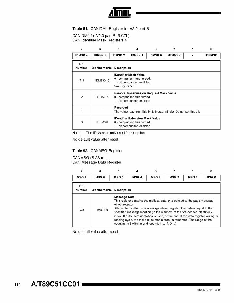
114 A/T89C51CC014129N–CAN–03/08
Table 91. CANIDM4 Register for V2.0 part B
CANIDM4 for V2.0 part B (S:C7h)
CAN Identifier Mask Registers 4
Note: The ID Mask is only used for reception.
No default value after reset.
Table 92. CANMSG Register
CANMSG (S:A3h)
CAN Message Data Register
No default value after reset.
7 6 5 4 3 2 1 0
IDMSK 4 IDMSK 3 IDMSK 2 IDMSK 1 IDMSK 0 RTRMSK - IDEMSK
Bit
Number Bit Mnemonic Description
7-3 IDMSK4:0
IDentifier Mask Value
0 - comparison true forced.
1 - bit comparison enabled.
See Figure 50.
2 RTRMSK
Remote Transmission Request Mask Value
0 - comparison true forced.
1 - bit comparison enabled.
1 -Reserved
The value read from this bit is indeterminate. Do not set this bit.
0 IDEMSK
IDentifier Extension Mask Value
0 - comparison true forced.
1 - bit comparison enabled.
7 6 5 4 3 2 1 0
MSG 7 MSG 6 MSG 5 MSG 4 MSG 3 MSG 2 MSG 1 MSG 0
Bit
Number Bit Mnemonic Description
7-0 MSG7:0
Message Data
This register contains the mailbox data byte pointed at the page message
object register.
After writing in the page message object register, this byte is equal to the
specified message location (in the mailbox) of the pre-defined identifier +
index. If auto-incrementation is used, at the end of the data register writing or
reading cycle, the mailbox pointer is auto-incremented. The range of the
counting is 8 with no end loop (0, 1,..., 7, 0,...)

115
A/T89C51CC01
4129N–CAN–03/08
Table 93. CANTCON Register
CANTCON (S:A1h)
CAN Timer ClockControl
Reset Value = 00h
Table 94. CANTIMH Register
CANTIMH (S:ADh)
CAN Timer High
Reset Value = 0000 0000b
Table 95. CANTIML Register
CANTIML (S:ACh)
CAN Timer Low
Reset Value = 0000 0000b
7 6 5 4 3 2 1 0
TPRESC 7 TPRESC 6 TPRESC 5 TPRESC 4 TPRESC 3 TPRESC 2 TPRESC 1 TPRESC 0
Bit
Number Bit Mnemonic Description
7-0 TPRESC7:0
Timer Prescaler of CAN Timer
This register is a prescaler for the main timer upper counter
range = 0 to 255.
See Figure 51.
7 6 5 4 3 2 1 0
CANGTIM
15
CANGTIM
14
CANGTIM
13
CANGTIM
12
CANGTIM
11
CANGTIM
10 CANGTIM 9 CANGTIM 8
Bit
Number Bit Mnemonic Description
7-0 CANGTIM15:8High byte of Message Timer
See Figure 51.
7 6 5 4 3 2 1 0
CANGTIM 7 CANGTIM 6 CANGTIM 5 CANGTIM 4 CANGTIM 3 CANGTIM 2 CANGTIM 1 CANGTIM 0
Bit
Number Bit Mnemonic Description
7-0 CANGTIM7:0Low byte of Message Timer
See Figure 51.

116 A/T89C51CC014129N–CAN–03/08
Table 96. CANSTMPH Register
CANSTMPH (S:AFh Read Only)
CAN Stamp Timer High
No default value after reset
Table 97. CANSTMPL Register
CANSTMPL (S:AEh Read Only)
CAN Stamp Timer Low
No default value after reset
Table 98. CANTTCH Register
CANTTCH (S:A5h Read Only)
CAN TTC Timer High
Reset Value = 0000 0000b
7 6 5 4 3 2 1 0
TIMSTMP
15
TIMSTMP
14
TIMSTMP
13
TIMSTMP
12
TIMSTMP
11
TIMSTMP
10 TIMSTMP 9 TIMSTMP 8
Bit
Number Bit Mnemonic Description
7-0 TIMSTMP15:8High byte of Time Stamp
See Figure 51.
7 6 5 4 3 2 1 0
TIMSTMP 7 TIMSTMP 6 TIMSTMP 5 TIMSTMP 4 TIMSTMP 3 TIMSTMP 2 TIMSTMP 1 TIMSTMP 0
Bit
Number Bit Mnemonic Description
7-0 TIMSTMP7:0Low byte of Time Stamp
See Figure 51.
7 6 5 4 3 2 1 0
TIMTTC 15 TIMTTC 14 TIMTTC 13 TIMTTC 12 TIMTTC 11 TIMTTC 10 TIMTTC 9 TIMTTC 8
Bit
Number Bit Mnemonic Description
7-0 TIMTTC15:8High byte of TTC Timer
See Figure 51.

117
A/T89C51CC01
4129N–CAN–03/08
Table 99. CANTTCL Register
CANTTCL (S:A4h Read Only)
CAN TTC Timer Low
Reset Value = 0000 0000b
7 6 5 4 3 2 1 0
TIMTTC 7 TIMTTC 6 TIMTTC 5 TIMTTC 4 TIMTTC 3 TIMTTC 2 TIMTTC 1 TIMTTC 0
Bit
Number Bit Mnemonic Description
7-0 TIMTTC7:0Low byte of TTC Timer
See Figure 51.

118 A/T89C51CC014129N–CAN–03/08
Programmable
Counter Array (PCA)
The PCA provides more timing capabilities with less CPU intervention than the standard
timer/counters. Its advantages include reduced software overhead and improved accu-
racy. The PCA consists of a dedicated timer/counter which serves as the time base for
an array of five compare/capture modules. Its clock input can be programmed to count
any of the following signals:
• PCA clock frequency/6 (see “clock” section)
• PCA clock frequency/2
• Timer 0 overflow
• External input on ECI (P1.2)
Each compare/capture modules can be programmed in any one of the following modes:
• rising and/or falling edge capture,
• software timer,
• high-speed output,
• pulse width modulator.
Module 4 can also be programmed as a Watchdog timer. see the "PCA Watchdog
Timer" section.
When the compare/capture modules are programmed in capture mode, software timer,
or high speed output mode, an interrupt can be generated when the module executes its
function. All five modules plus the PCA timer overflow share one interrupt vector.
The PCA timer/counter and compare/capture modules share Port 1 for external I/Os.
These pins are listed below. If the pin is not used for the PCA, it can still be used for
standard I/O.
PCA Timer The PCA timer is a common time base for all five modules (see Figure 53). The timer
count source is determined from the CPS1 and CPS0 bits in the CMOD SFR (see Table
8) and can be programmed to run at:
• 1/6 the PCA clock frequency.
• 1/2 the PCA clock frequency.
• the Timer 0 overflow.
• the input on the ECI pin (P1.2).
PCA Component External I/O Pin
16-bit Counter P1.2/ECI
16-bit Module 0 P1.3/CEX0
16-bit Module 1 P1.4/CEX1
16-bit Module 2 P1.5/CEX2
16-bit Module 3 P1.6/CEX3
16-bit Module 4 P1.7/CEX4
119
A/T89C51CC01
4129N–CAN–03/08
Figure 53. PCA Timer/Counter
The CMOD register includes three additional bits associated with the PCA.
• The CIDL bit which allows the PCA to stop during idle mode.
• The WDTE bit which enables or disables the Watchdog function on module 4.
• The ECF bit which when set causes an interrupt and the PCA overflow flag CF in
CCON register to be set when the PCA timer overflows.
The CCON register contains the run control bit for the PCA and the flags for the PCA
timer and each module.
• The CR bit must be set to run the PCA. The PCA is shut off by clearing this bit.
• The CF bit is set when the PCA counter overflows and an interrupt will be generated
if the ECF bit in CMOD register is set. The CF bit can only be cleared by software.
• The CCF0:4 bits are the flags for the modules (CCF0 for module0...) and are set by
hardware when either a match or a capture occurs. These flags also can be cleared
by software.
PCA Modules Each one of the five compare/capture modules has six possible functions. It can
perform:
• 16-bit Capture, positive-edge triggered
• 16-bit Capture, negative-edge triggered
• 16-bit Capture, both positive and negative-edge triggered
• 16-bit Software Timer
• 16-bit High Speed Output
• 8-bit Pulse Width Modulator.
In addition module 4 can be used as a Watchdog Timer.
CIDL CPS1 CPS0 ECF
ItCH CL
16 bit up counter
To PCAmodules
FPca/6
FPca/2
T0 OVF
P1.2
Idle
CMOD0xD9WDTE
CF CRCCON0xD8CCF4 CCF3 CCF2 CCF1 CCF0
overflow

120 A/T89C51CC014129N–CAN–03/08
Each module in the PCA has a special function register associated with it (CCAPM0 for
module 0 ...). The CCAPM0:4 registers contain the bits that control the mode that each
module will operate in.
• The ECCF bit enables the CCF flag in the CCON register to generate an interrupt
when a match or compare occurs in the associated module.
• The PWM bit enables the pulse width modulation mode.
• The TOG bit when set causes the CEX output associated with the module to toggle
when there is a match between the PCA counter and the module’s capture/compare
register.
• The match bit MAT when set will cause the CCFn bit in the CCON register to be set
when there is a match between the PCA counter and the module’s capture/compare
register.
• The two bits CAPN and CAPP in CCAPMn register determine the edge that a
capture input will be active on. The CAPN bit enables the negative edge, and the
CAPP bit enables the positive edge. If both bits are set both edges will be enabled.
• The bit ECOM in CCAPM register when set enables the comparator function.
PCA Interrupt
Figure 54. PCA Interrupt System
PCA Capture Mode To use one of the PCA modules in capture mode either one or both of the CCAPM bits
CAPN and CAPP for that module must be set. The external CEX input for the module
(on port 1) is sampled for a transition. When a valid transition occurs the PCA hardware
loads the value of the PCA counter registers (CH and CL) into the module’s capture reg-
isters (CCAPnL and CCAPnH). If the CCFn bit for the module in the CCON SFR and the
ECCFn bit in the CCAPMn SFR are set then an interrupt will be generated.
CF CRCCON
CCF4 CCF3 CCF2 CCF1 CCF0
Module 4
Module 3
Module 2
Module 1
Module 0
PCA Timer/Counter
ECCFn
CCAPMn.0
To Interrupt
EAIEN0.7
ECIEN0.6
ECFCMOD.0

121
A/T89C51CC01
4129N–CAN–03/08
Figure 55. PCA Capture Mode
16-bit Software Timer Mode
The PCA modules can be used as software timers by setting both the ECOM and MAT
bits in the modules CCAPMn register. The PCA timer will be compared to the module’s
capture registers and when a match occurs an interrupt will occur if the CCFn (CCON
SFR) and the ECCFn (CCAPMn SFR) bits for the module are both set.
Figure 56. PCA 16-bit Software Timer and High Speed Output Mode
CEXn
n = 0, 4
PCA Counter
CH(8bits)
CL(8bits)
CCAPnH CCAPnL
CCFn
CCON
PCA
Interrupt
Request
- 0CAPPn CAPNn 000 ECCFn
7
CCAPMn Register (n = 0, 4)0
CCAPnL(8 bits)
CCAPnH(8 bits)
- ECOMn0 0 MATn TOGn0 ECCFn
7 0
CCAPMn Register
(n = 0, 4)
CH(8 bits)
CL(8 bits)
16-Bit ComparatorMatch
EnableCCFn
CCON reg
PCA
Interrupt
Request
CEXn
Compare/Capture ModulePCA Counter
“0”
“1”
Reset
Write to
CCAPnL
Write to CCAPnH
For software Timer mode, set ECOMn and MATn.
For high speed output mode, set ECOMn, MATn and TOGn.
Toggle

122 A/T89C51CC014129N–CAN–03/08
High Speed Output Mode In this mode the CEX output (on port 1) associated with the PCA module will toggle
each time a match occurs between the PCA counter and the module’s capture registers.
To activate this mode the TOG, MAT, and ECOM bits in the module’s CCAPMn SFR
must be set.
Figure 57. PCA High Speed Output Mode
Pulse Width Modulator Mode
All the PCA modules can be used as PWM outputs. The output frequency depends on
the source for the PCA timer. All the modules will have the same output frequency
because they all share the PCA timer. The duty cycle of each module is independently
variable using the module’s capture register CCAPLn. When the value of the PCA CL
SFR is less than the value in the module’s CCAPLn SFR the output will be low, when it
is equal to or greater than it, the output will be high. When CL overflows from FF to 00,
CCAPLn is reloaded with the value in CCAPHn. the allows the PWM to be updated with-
out glitches. The PWM and ECOM bits in the module’s CCAPMn register must be set to
enable the PWM mode.
CH CL
CCAPnH CCAPnL
ECOMnCCAPMn, n = 0 to 4
0xDA to 0xDECAPNn MATn TOGn PWMn ECCFnCAPPn
16-bit comparatorMatch
CF CRCCON
0xD8CCF4 CCF3 CCF2 CCF1 CCF0
PCA IT
Enable
CEXn
PCA counter/timer
“1”“0”
Write toCCAPnL
ResetWrite to
CCAPnH

123
A/T89C51CC01
4129N–CAN–03/08
Figure 58. PCA PWM Mode
PCA Watchdog Timer An on-board Watchdog timer is available with the PCA to improve system reliability with-
out increasing chip count. Watchdog timers are useful for systems that are sensitive to
noise, power glitches, or electrostatic discharge. Module 4 is the only PCA module that
can be programmed as a Watchdog. However, this module can still be used for other
modes if the Watchdog is not needed. The user pre-loads a 16-bit value in the compare
registers. Just like the other compare modes, this 16-bit value is compared to the PCA
timer value. If a match is allowed to occur, an internal reset will be generated. This will
not cause the RST pin to be driven high.
To hold off the reset, the user has three options:
• periodically change the compare value so it will never match the PCA timer,
• periodically change the PCA timer value so it will never match the compare values,
or
• disable the Watchdog by clearing the WDTE bit before a match occurs and then re-
enable it.
The first two options are more reliable because the Watchdog timer is never disabled as
in the third option. If the program counter ever goes astray, a match will eventually occur
and cause an internal reset. If other PCA modules are being used the second option not
recommended either. Remember, the PCA timer is the time base for all modules;
changing the time base for other modules would not be a good idea. Thus, in most appli-
cations the first solution is the best option.
CL rolls over from FFh TO 00h loads
CCAPnH contents into CCAPnL
CCAPnL
CCAPnH
8-Bit
ComparatorCL (8 bits)
“0”
“1”
CL < CCAPnL
CL > = CCAPnL
CEX
PWMnCCAPMn.1
ECOMnCCAPMn.6
124 A/T89C51CC014129N–CAN–03/08
PCA Registers Table 100. CMOD Register
CMOD (S:D9h)
PCA Counter Mode Register
Reset Value = 00XX X000b
7 6 5 4 3 2 1 0
CIDL WDTE - - - CPS1 CPS0 ECF
Bit
Number
Bit
Mnemonic Description
7 CIDL
PCA Counter Idle Control bit
Clear to let the PCA run during Idle mode.
Set to stop the PCA when Idle mode is invoked.
6 WDTE
Watchdog Timer Enable
Clear to disable Watchdog Timer function on PCA Module 4,
Set to enable it.
5 -Reserved
The value read from this bit is indeterminate. Do not set this bit.
4 -Reserved
The value read from this bit is indeterminate. Do not set this bit.
3 -Reserved
The value read from this bit is indeterminate. Do not set this bit.
2-1 CPS1:0
EWC Count Pulse Select bits
CPS1 CPS0 Clock source
0 0 Internal Clock, FPca/6
0 1 Internal Clock, FPca/2
1 0 Timer 0 overflow
1 1 External clock at ECI/P1.2 pin (Max. Rate = FPca/4)
0 ECF
Enable PCA Counter Overflow Interrupt bit
Clear to disable CF bit in CCON register to generate an interrupt.
Set to enable CF bit in CCON register to generate an interrupt.

125
A/T89C51CC01
4129N–CAN–03/08
Table 101. CCON Register
CCON (S:D8h)
PCA Counter Control Register
Reset Value = 00X0 0000b
7 6 5 4 3 2 1 0
CF CR - CCF4 CCF3 CCF2 CCF1 CCF0
Bit
Number
Bit
Mnemonic Description
7 CF
PCA Timer/Counter Overflow flag
Set by hardware when the PCA Timer/Counter rolls over. This generates a PCA
interrupt request if the ECF bit in CMOD register is set.
Must be cleared by software.
6 CR
PCA Timer/Counter Run Control bit
Clear to turn the PCA Timer/Counter off.
Set to turn the PCA Timer/Counter on.
5 -Reserved
The value read from this bit is indeterminate. Do not set this bit.
4 CCF4
PCA Module 4 Compare/Capture flag
Set by hardware when a match or capture occurs. This generates a PCA
interrupt request if the ECCF 4 bit in CCAPM 4 register is set.
Must be cleared by software.
3 CCF3
PCA Module 3 Compare/Capture flag
Set by hardware when a match or capture occurs. This generates a PCA
interrupt request if the ECCF 3 bit in CCAPM 3 register is set.
Must be cleared by software.
2 CCF2
PCA Module 2 Compare/Capture flag
Set by hardware when a match or capture occurs. This generates a PCA
interrupt request if the ECCF 2 bit in CCAPM 2 register is set.
Must be cleared by software.
1 CCF1
PCA Module 1 Compare/Capture flag
Set by hardware when a match or capture occurs. This generates a PCA
interrupt request if the ECCF 1 bit in CCAPM 1 register is set.
Must be cleared by software.
0 CCF0
PCA Module 0 Compare/Capture flag
Set by hardware when a match or capture occurs. This generates a PCA
interrupt request if the ECCF 0 bit in CCAPM 0 register is set.
Must be cleared by software.

126 A/T89C51CC014129N–CAN–03/08
Table 102. CCAPnH Registers
CCAP0H (S:FAh)
CCAP1H (S:FBh)
CCAP2H (S:FCh)
CCAP3H (S:FDh)
CCAP4H (S:FEh)
PCA High Byte Compare/Capture Module n Register (n=0..4)
Reset Value = 0000 0000b
Table 103. CCAPnL Registers
CCAP0L (S:EAh)
CCAP1L (S:EBh)
CCAP2L (S:ECh)
CCAP3L (S:EDh)
CCAP4L (S:EEh)
PCA Low Byte Compare/Capture Module n Register (n=0..4)
Reset Value = 0000 0000b
7 6 5 4 3 2 1 0
CCAPnH 7 CCAPnH 6 CCAPnH 5 CCAPnH 4 CCAPnH 3 CCAPnH 2 CCAPnH 1 CCAPnH 0
Bit
Number
Bit
Mnemonic Description
7:0CCAPnH
7:0High byte of EWC-PCA comparison or capture values
7 6 5 4 3 2 1 0
CCAPnL 7 CCAPnL 6 CCAPnL 5 CCAPnL 4 CCAPnL 3 CCAPnL 2 CCAPnL 1 CCAPnL 0
Bit
Number
Bit
Mnemonic Description
7:0CCAPnL
7:0Low byte of EWC-PCA comparison or capture values

127
A/T89C51CC01
4129N–CAN–03/08
Table 104. CCAPMn Registers
CCAPM0 (S:DAh)
CCAPM1 (S:DBh)
CCAPM2 (S:DCh)
CCAPM3 (S:DDh)
CCAPM4 (S:DEh)
PCA Compare/Capture Module n Mode registers (n=0..4)
Reset Value = X000 0000b
7 6 5 4 3 2 1 0
- ECOMn CAPPn CAPNn MATn TOGn PWMn ECCFn
Bit
Number
Bit
Mnemonic Description
7 -Reserved
The Value read from this bit is indeterminate. Do not set this bit.
6 ECOMn
Enable Compare Mode Module x bit
Clear to disable the Compare function.
Set to enable the Compare function.
The Compare function is used to implement the software Timer, the high-speed
output, the Pulse Width Modulator (PWM) and the Watchdog Timer (WDT).
5 CAPPn
Capture Mode (Positive) Module x bit
Clear to disable the Capture function triggered by a positive edge on CEXx pin.
Set to enable the Capture function triggered by a positive edge on CEXx pin
4 CAPNn
Capture Mode (Negative) Module x bit
Clear to disable the Capture function triggered by a negative edge on CEXx pin.
Set to enable the Capture function triggered by a negative edge on CEXx pin.
3 MATn
Match Module x bit
Set when a match of the PCA Counter with the Compare/Capture register sets
CCFx bit in CCON register, flagging an interrupt.
2 TOGn
Toggle Module x bit
The toggle mode is configured by setting ECOMx, MATx and TOGx bits.
Set when a match of the PCA Counter with the Compare/Capture register
toggles the CEXx pin.
1 PWMn
Pulse Width Modulation Module x Mode bit
Set to configure the module x as an 8-bit Pulse Width Modulator with output
waveform on CEXx pin.
0 ECCFn
Enable CCFx Interrupt bit
Clear to disable CCFx bit in CCON register to generate an interrupt request.
Set to enable CCFx bit in CCON register to generate an interrupt request.

128 A/T89C51CC014129N–CAN–03/08
Table 105. CH Register
CH (S:F9h)
PCA Counter Register High Value
Reset Value = 0000 00000b
Table 106. CL Register
CL (S:E9h)
PCA counter Register Low Value
Reset Value = 0000 00000b
7 6 5 4 3 2 1 0
CH 7 CH 6 CH 5 CH 4 CH 3 CH 2 CH 1 CH 0
Bit
Number
Bit
Mnemonic Description
7:0 CH 7:0 High byte of Timer/Counter
7 6 5 4 3 2 1 0
CL 7 CL 6 CL 5 CL 4 CL 3 CL 2 CL 1 CL 0
Bit
Number
Bit
Mnemonic Description
7:0 CL0 7:0 Low byte of Timer/Counter

129
A/T89C51CC01
4129N–CAN–03/08
Analog-to-Digital
Converter (ADC)
This section describes the on-chip 10 bit analog-to-digital converter of the
T89C51CC01. Eight ADC channels are available for sampling of the external sources
AN0 to AN7. An analog multiplexer allows the single ADC converter to select one from
the 8 ADC channels as ADC input voltage (ADCIN). ADCIN is converted by the 10-bit
cascaded potentiometric ADC.
Two modes of conversion are available:
- Standard conversion (8 bits).
- Precision conversion (10 bits).
For the precision conversion, set bit PSIDLE in ADCON register and start conversion.
The device is in a pseudo-idle mode, the CPU does not run but the peripherals are
always running. This mode allows digital noise to be as low as possible, to ensure high
precision conversion.
For this mode it is necessary to work with end of conversion interrupt, which is the only
way to wake the device up.
If another interrupt occurs during the precision conversion, it will be served only after
this conversion is completed.
Features • 8 channels with multiplexed inputs
• 10-bit cascaded potentiometric ADC
• Conversion time 16 micro-seconds (typ.)
• Zero Error (offset) ± 2 LSB max
• Positive External Reference Voltage Range (VAREF) 2.4 to 3.0 Volt (typ.)
• ADCIN Range 0 to 3Volt
• Integral non-linearity typical 1 LSB, max. 2 LSB
• Differential non-linearity typical 0.5 LSB, max. 1 LSB
• Conversion Complete Flag or Conversion Complete Interrupt
• Selectable ADC Clock
ADC Port 1 I/O Functions Port 1 pins are general I/O that are shared with the ADC channels. The channel select
bit in ADCF register define which ADC channel/port1 pin will be used as ADCIN. The
remaining ADC channels/port1 pins can be used as general-purpose I/O or as the alter-
nate function that is available.
A conversion launched on a channel which are not selected on ADCF register will not
have any effect.
VAREF VAREF should be connected to a low impedance point and must remain in the range
specified in Table 122. If the ADC is not used, it is recommended to connect VAREF to
VAGND.

130 A/T89C51CC014129N–CAN–03/08
Figure 59. ADC Description
Figure 60 shows the timing diagram of a complete conversion. For simplicity, the figure
depicts the waveforms in idealized form and do not provide precise timing information.
For ADC characteristics and timing parameters refer to the Section “AC Characteristics”
of the T89C51CC01 datasheet.
Figure 60. Timing Diagram
Notes: 1. Tsetup min, see the AC Parameter for A/D conversion.
2. Tconv = 11 clock ADC = 1sample and hold + 10 bit conversion
The user must ensure that Tsetup time between setting ADEN and the start of the first conversion.
Rai
AN0/P1.0
AN1/P1.1
AN2/P1.2
AN3/P1.3
AN4/P1.4
AN5/P1.5
AN6/P1.6
AN7/P1.7
000
001
010
011
100
101
110
111
SCH2ADCON.2
SCH0ADCON.0
SCH1ADCON.1
ADCCLOCK
ADENADCON.5
ADSSTADCON.3
ADEOCADCON.4 ADC
InterruptRequest
EADCIEN1.1
CONTROL
AVSS
Sample and Hold
ADDH
VAREF
R/2R DAC
VAGND
8
10
+
-
ADDL2SAR
ADCIN
Cai
ADEN
ADSST
ADEOC
TSETUP (1)
TCONV (2)
CLK

131
A/T89C51CC01
4129N–CAN–03/08
ADC Converter Operation
A start of single A/D conversion is triggered by setting bit ADSST (ADCON.3).
After completion of the A/D conversion, the ADSST bit is cleared by hardware.
The end-of-conversion flag ADEOC (ADCON.4) is set when the value of conversion is
available in ADDH and ADDL, it must be cleared by software. If the bit EADC (IEN1.1) is
set, an interrupt occur when flag ADEOC is set (see Figure 62). Clear this flag for re-
arming the interrupt.
The bits SCH0 to SCH2 in ADCON register are used for the analog input channel
selection.(1)
Note: 1. Always leave Tsetup time before starting a conversion unless ADEN is permanently
high. In this case one should wait Tsetup only before the first conversion.
Table 107. Selected Analog input
Voltage Conversion When the ADCIN is equals to VAREF the ADC converts the signal to 3FFh (full scale). If
the input voltage equals VAGND, the ADC converts it to 000h. Input voltage between
VAREF and VAGND are a straight-line linear conversion. All other voltages will result in
3FFh if greater than VAREF and 000h if less than VAGND.
Note: ADCIN should not exceed VAREF absolute maximum range (see “Absolute Maximum
Ratings” on page 144)
Clock Selection The ADC clock is the same as CPU.
The maximum clock frequency is defined in the DC parmeters for A/D converter. A pres-
caler is featured (ADCCLK) to generate the ADC clock from the oscillator frequency.
if PRS > 0 then fADC = Fperiph / 2 x PRS
if PRS = 0 then fADC = Fperiph / 64
SCH2 SCH1 SCH0 Selected Analog input
0 0 0 AN0
0 0 1 AN1
0 1 0 AN2
0 1 1 AN3
1 0 0 AN4
1 0 1 AN5
1 1 0 AN6
1 1 1 AN7
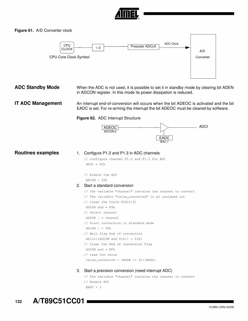
132 A/T89C51CC014129N–CAN–03/08
Figure 61. A/D Converter clock
ADC Standby Mode When the ADC is not used, it is possible to set it in standby mode by clearing bit ADEN
in ADCON register. In this mode its power dissipation is reduced.
IT ADC Management An interrupt end-of-conversion will occurs when the bit ADEOC is activated and the bit
EADC is set. For re-arming the interrupt the bit ADEOC must be cleared by software.
Figure 62. ADC Interrupt Structure
Routines examples 1. Configure P1.2 and P1.3 in ADC channels
// configure channel P1.2 and P1.3 for ADC
ADCF = 0Ch
// Enable the ADC
ADCON = 20h
2. Start a standard conversion
// The variable "channel" contains the channel to convert
// The variable "value_converted" is an unsigned int
// Clear the field SCH[2:0]
ADCON and = F8h
// Select channel
ADCON | = channel
// Start conversion in standard mode
ADCON | = 08h
// Wait flag End of conversion
while((ADCON and 01h)! = 01h)
// Clear the End of conversion flag
ADCON and = EFh
// read the value
value_converted = (ADDH << 2)+(ADDL)
3. Start a precision conversion (need interrupt ADC)
// The variable "channel" contains the channel to convert
// Enable ADC
EADC = 1
Prescaler ADCLK
A/D
Converter
ADC ClockCPU
CLOCK
CPU Core Clock Symbol
÷ 2
ADEOCADCON.2
EADCIEN1.1
ADCI

133
A/T89C51CC01
4129N–CAN–03/08
// clear the field SCH[2:0]
ADCON and = F8h
// Select the channel
ADCON | = channel
// Start conversion in precision mode
ADCON | = 48h
Note: to enable the ADC interrupt:
EA = 1

134 A/T89C51CC014129N–CAN–03/08
Registers Table 108. ADCF Register
ADCF (S:F6h)
ADC Configuration
Reset Value = 0000 0000b
Table 109. ADCON Register
ADCON (S:F3h)
ADC Control Register
Reset Value = X000 0000b
7 6 5 4 3 2 1 0
CH 7 CH 6 CH 5 CH 4 CH 3 CH 2 CH 1 CH 0
Bit
Number
Bit
Mnemonic Description
7-0 CH 0:7
Channel Configuration
Set to use P1.x as ADC input.
Clear to use P1.x as standart I/O port.
7 6 5 4 3 2 1 0
- PSIDLE ADEN ADEOC ADSST SCH2 SCH1 SCH0
Bit
Number
Bit
Mnemonic Description
7 -
6 PSIDLE
Pseudo Idle Mode (Best Precision)
Set to put in idle mode during conversion
Clear to convert without idle mode.
5 ADEN
Enable/Standby Mode
Set to enable ADC
Clear for Standby mode (power dissipation 1 uW).
4 ADEOC
End Of Conversion
Set by hardware when ADC result is ready to be read. This flag can generate an
interrupt.
Must be cleared by software.
3 ADSST
Start and Status
Set to start an A/D conversion.
Cleared by hardware after completion of the conversion
2-0 SCH2:0Selection of Channel to Convert
see Table 107

135
A/T89C51CC01
4129N–CAN–03/08
Table 110. ADCLK Register
ADCLK (S:F2h)
ADC Clock Prescaler
Reset Value = XXX0 0000b
Table 111. ADDH Register
ADDH (S:F5h Read Only)
ADC Data High Byte Register
Reset Value = 00h
Table 112. ADDL Register
ADDL (S:F4h Read Only)
ADC Data Low Byte Register
Reset Value = 00h
7 6 5 4 3 2 1 0
- - - PRS 4 PRS 3 PRS 2 PRS 1 PRS 0
Bit
Number
Bit
Mnemonic Description
7-5 -Reserved
The value read from these bits are indeterminate. Do not set these bits.
4-0 PRS4:0Clock Prescaler
fADC = fcpu clock/ (4 (or 2 in X2 mode)* PRS )
7 6 5 4 3 2 1 0
ADAT 9 ADAT 8 ADAT 7 ADAT 6 ADAT 5 ADAT 4 ADAT 3 ADAT 2
Bit
Number
Bit
Mnemonic Description
7-0 ADAT9:2ADC result
bits 9-2
7 6 5 4 3 2 1 0
- - - - - - ADAT 1 ADAT 0
Bit
Number
Bit
Mnemonic Description
7-2 -Reserved
The value read from these bits are indeterminate. Do not set these bits.
1-0 ADAT1:0ADC result
bits 1-0
136 A/T89C51CC014129N–CAN–03/08
Interrupt System
Introduction The CAN Controller has a total of 10 interrupt vectors: two external interrupts (INT0 and
INT1), three timer interrupts (timers 0, 1 and 2), a serial port interrupt, a PCA, a CAN
interrupt, a timer overrun interrupt and an ADC. These interrupts are shown below.
Figure 63. Interrupt Control System
ECANIEN1.0
EX0IEN0.0
00
01
10
11
ExternalInterrupt 0INT0#
EAIEN0.7
EX1IEN0.2
ExternalInterrupt 1INT1#
ET0IEN0.1
Timer 0
ECIEN0.6
PCA
ET1IEN0.3
Timer 1
ESIEN0.4
UART
EADCIEN1.1
A to DConverter
ETIMIEN1.2
CAN Timer
CAN
Interrupt Enable Lowest Priority Interrupts
Highest
Priority Enable
00
01
10
11
00
01
10
11
00
01
10
11
00
01
10
11
00
01
10
11
00
01
10
11
00
01
10
11
00
01
10
11
PriorityInterrupts
TxDC
RxDC
AIN1:0
IPH/L
controller
Timer 2
00
01
10
11
ET2IEN0.5
TxD
RxD
CEX0:5

137
A/T89C51CC01
4129N–CAN–03/08
Each of the interrupt sources can be individually enabled or disabled by setting or clear-
ing a bit in the Interrupt Enable register. This register also contains a global disable bit
which must be cleared to disable all the interrupts at the same time.
Each interrupt source can also be individually programmed to one of four priority levels
by setting or clearing a bit in the Interrupt Priority registers. The Table below shows the
bit values and priority levels associated with each combination.
Table 113. Priority Level Bit Values
A low-priority interrupt can be interrupted by a high priority interrupt but not by another
low-priority interrupt. A high-priority interrupt cannot be interrupted by any other interrupt
source.
If two interrupt requests of different priority levels are received simultaneously, the
request of the higher priority level is serviced. If interrupt requests of the same priority
level are received simultaneously, an internal polling sequence determines which
request is serviced. Thus within each priority level there is a second priority structure
determined by the polling sequence, see Table 114.
Table 114. Interrupt Priority Within level
IPH.x IPL.x Interrupt Level Priority
0 0 0 (Lowest)
0 1 1
1 0 2
1 1 3 (Highest)
Interrupt Name Interrupt Address Vector Interrupt Number Polling Priority
external interrupt (INT0) 0003h 1 1
Timer 0 (TF0) 000Bh 2 2
external interrupt (INT1) 0013h 3 3
Timer 1 (TF1) 001Bh 4 4
PCA (CF or CCFn) 0033h 7 5
UART (RI or TI) 0023h 5 6
Timer 2 (TF2) 002Bh 6 7
CAN (Txok, Rxok, Err or
OvrBuf)003Bh 8 8
ADC (ADCI) 0043h 9 9
CAN Timer Overflow (OVRTIM) 004Bh 10 10
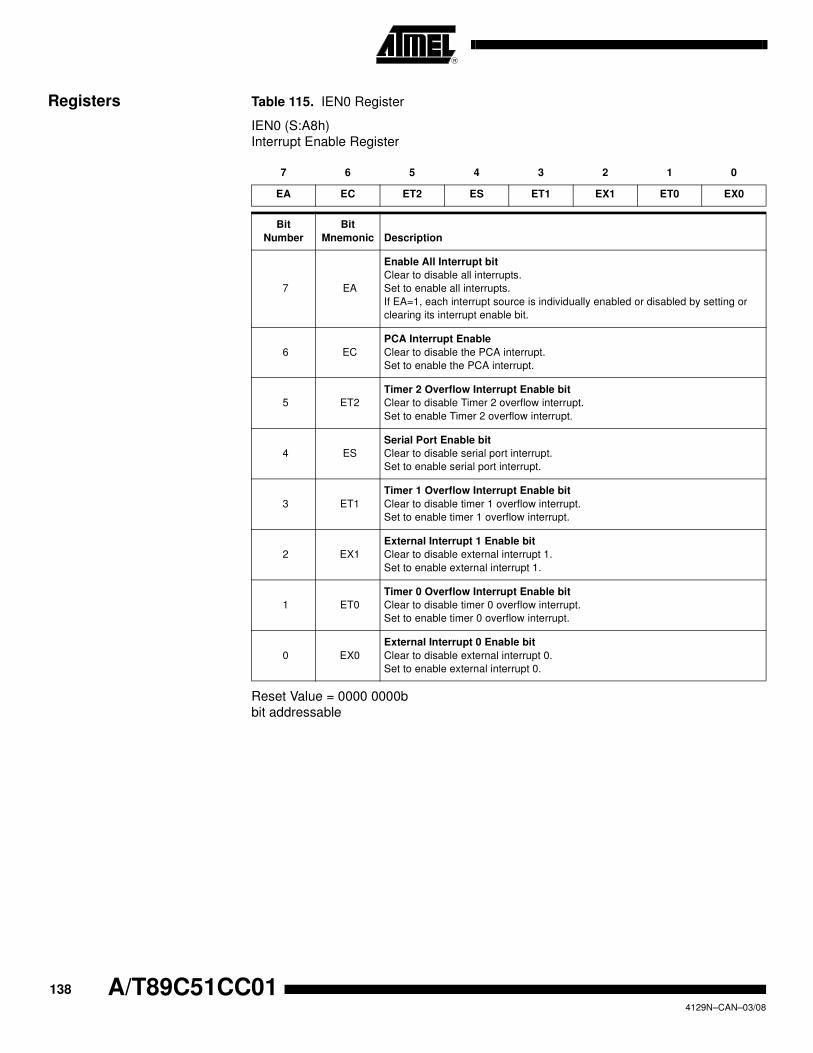
138 A/T89C51CC014129N–CAN–03/08
Registers Table 115. IEN0 Register
IEN0 (S:A8h)
Interrupt Enable Register
Reset Value = 0000 0000b
bit addressable
7 6 5 4 3 2 1 0
EA EC ET2 ES ET1 EX1 ET0 EX0
Bit
Number
Bit
Mnemonic Description
7 EA
Enable All Interrupt bit
Clear to disable all interrupts.
Set to enable all interrupts.
If EA=1, each interrupt source is individually enabled or disabled by setting or
clearing its interrupt enable bit.
6 EC
PCA Interrupt Enable
Clear to disable the PCA interrupt.
Set to enable the PCA interrupt.
5 ET2
Timer 2 Overflow Interrupt Enable bit
Clear to disable Timer 2 overflow interrupt.
Set to enable Timer 2 overflow interrupt.
4 ES
Serial Port Enable bit
Clear to disable serial port interrupt.
Set to enable serial port interrupt.
3 ET1
Timer 1 Overflow Interrupt Enable bit
Clear to disable timer 1 overflow interrupt.
Set to enable timer 1 overflow interrupt.
2 EX1
External Interrupt 1 Enable bit
Clear to disable external interrupt 1.
Set to enable external interrupt 1.
1 ET0
Timer 0 Overflow Interrupt Enable bit
Clear to disable timer 0 overflow interrupt.
Set to enable timer 0 overflow interrupt.
0 EX0
External Interrupt 0 Enable bit
Clear to disable external interrupt 0.
Set to enable external interrupt 0.

139
A/T89C51CC01
4129N–CAN–03/08
Table 116. IEN1 Register
IEN1 (S:E8h)
Interrupt Enable Register
Reset Value = xxxx x000b
bit addressable
7 6 5 4 3 2 1 0
- - - - - ETIM EADC ECAN
Bit
Number
Bit
Mnemonic Description
7 -Reserved
The value read from this bit is indeterminate. Do not set this bit.
6 -Reserved
The value read from this bit is indeterminate. Do not set this bit.
5 -Reserved
The value read from this bit is indeterminate. Do not set this bit.
4 -Reserved
The value read from this bit is indeterminate. Do not set this bit.
3 -Reserved
The value read from this bit is indeterminate. Do not set this bit.
2 ETIM
TImer Overrun Interrupt Enable bit
Clear to disable the timer overrun interrupt.
Set to enable the timer overrun interrupt.
1 EADC
ADC Interrupt Enable bit
Clear to disable the ADC interrupt.
Set to enable the ADC interrupt.
0 ECAN
CAN Interrupt Enable bit
Clear to disable the CAN interrupt.
Set to enable the CAN interrupt.

140 A/T89C51CC014129N–CAN–03/08
Table 117. IPL0 Register
IPL0 (S:B8h)
Interrupt Enable Register
Reset Value = X000 0000b
bit addressable
7 6 5 4 3 2 1 0
- PPC PT2 PS PT1 PX1 PT0 PX0
Bit
Number
Bit
Mnemonic Description
7 -Reserved
The value read from this bit is indeterminate. Do not set this bit.
6 PPCPCA Interrupt Priority bit
Refer to PPCH for priority level
5 PT2Timer 2 Overflow Interrupt Priority bit
Refer to PT2H for priority level.
4 PSSerial Port Priority bit
Refer to PSH for priority level.
3 PT1Timer 1 Overflow Interrupt Priority bit
Refer to PT1H for priority level.
2 PX1External Interrupt 1 Priority bit
Refer to PX1H for priority level.
1 PT0Timer 0 Overflow Interrupt Priority bit
Refer to PT0H for priority level.
0 PX0External Interrupt 0 Priority bit
Refer to PX0H for priority level.

141
A/T89C51CC01
4129N–CAN–03/08
Table 118. IPL1 Register
IPL1 (S:F8h)
Interrupt Priority Low Register 1
Reset Value = XXXX X000b
bit addressable
7 6 5 4 3 2 1 0
- - - - POVRL PADCL PCANL
Bit
Number
Bit
Mnemonic Description
7 -Reserved
The value read from this bit is indeterminate. Do not set this bit.
6 -Reserved
The value read from this bit is indeterminate. Do not set this bit.
5 -Reserved
The value read from this bit is indeterminate. Do not set this bit.
4 -Reserved
The value read from this bit is indeterminate. Do not set this bit.
3 -Reserved
The value read from this bit is indeterminate. Do not set this bit.
2 POVRLTimer Overrun Interrupt Priority Level Less Significant Bit
Refer to PI2CH for priority level.
1 PADCLADC Interrupt Priority Level Less Significant Bit
Refer to PSPIH for priority level.
0 PCANLCAN Interrupt Priority Level Less Significant Bit
Refer to PKBH for priority level.

142 A/T89C51CC014129N–CAN–03/08
Table 119. IPH0 Register
IPH0 (B7h)
Interrupt High Priority Register
Reset Value = X000 0000b
7 6 5 4 3 2 1 0
- PPCH PT2H PSH PT1H PX1H PT0H PX0H
Bit
Number
Bit
Mnemonic Description
7 -Reserved
The value read from this bit is indeterminate. Do not set this bit.
6 PPCH
PCA Interrupt Priority Level Most Significant bit
PPCH PPC Priority level
0 0 Lowest
0 1
1 0
1 1 Highest priority
5 PT2H
Timer 2 Overflow Interrupt High Priority bit
PT2H PT2 Priority Level
0 0 Lowest
0 1
1 0
1 1 Highest
4 PSH
Serial Port High Priority bit
PSH PS Priority Level
0 0 Lowest
0 1
1 0
1 1 Highest
3 PT1H
Timer 1 Overflow Interrupt High Priority bit
PT1H PT1 Priority Level
0 0 Lowest
0 1
1 0
1 1 Highest
2 PX1H
External Interrupt 1 High Priority bit
PX1H PX1 Priority Level
0 0 Lowest
0 1
1 0
1 1 Highest
1 PT0H
Timer 0 Overflow Interrupt High Priority bit
PT0H PT0 Priority Level
0 0 Lowest
0 1
1 0
1 1 Highest
0 PX0H
External Interrupt 0 high priority bit
PX0H PX0 Priority Level
0 0 Lowest
0 1
1 0
1 1 Highest
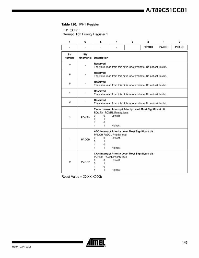
143
A/T89C51CC01
4129N–CAN–03/08
Table 120. IPH1 Register
IPH1 (S:F7h)
Interrupt High Priority Register 1
Reset Value = XXXX X000b
7 6 5 4 3 2 1 0
- - - - POVRH PADCH PCANH
Bit
Number
Bit
Mnemonic Description
7 -Reserved
The value read from this bit is indeterminate. Do not set this bit.
6 -Reserved
The value read from this bit is indeterminate. Do not set this bit.
5 -Reserved
The value read from this bit is indeterminate. Do not set this bit.
4 -Reserved
The value read from this bit is indeterminate. Do not set this bit.
3 -Reserved
The value read from this bit is indeterminate. Do not set this bit.
2 POVRH
Timer overrun Interrupt Priority Level Most Significant bit
POVRH POVRL Priority level
0 0 Lowest
0 1
1 0
1 1 Highest
1 PADCH
ADC Interrupt Priority Level Most Significant bit
PADCH PADCL Priority level
0 0 Lowest
0 1
1 0
1 1 Highest
0 PCANH
CAN Interrupt Priority Level Most Significant bit
PCANH PCANLPriority level
0 0 Lowest
0 1
1 0
1 1 Highest

144 A/T89C51CC014129N–CAN–03/08
Electrical Characteristics
Absolute Maximum Ratings
DC Parameters for Standard Voltage
TA = -40°C to +85°C; VSS = 0V; VCC = 3V to 5.5V; F = 0 to 40 MHz
Ambiant Temperature Under Bias:
I = industrial ....................................................... -40°C to 85°C
Storage Temperature .................................... -65°C to + 150°C
Voltage on VCC from VSS ......................................-0.5V to + 6V
Voltage on Any Pin from VSS.................... -0.5V to VCC + 0.2 V
Power Dissipation .............................................................. 1 W
Table 121. DC Parameters in Standard Voltage
Symbol Parameter Min Typ(5) Max Unit Test Conditions
VIL Input Low Voltage -0.5 0.2Vcc - 0.1 V
VIH Input High Voltage except XTAL1, RST 0.2 VCC + 0.9 VCC + 0.5 V
VIH1(8) Input High Voltage, XTAL1, RST 0.7 VCC VCC + 0.5 V
VOL Output Low Voltage, ports 1, 2, 3 and 4(6)
0.3
0.45
1.0
V
V
V
IOL = 100 µA(4)
IOL = 1.6 mA(4)
IOL = 3.5 mA(4)
VOL1 Output Low Voltage, port 0, ALE, PSEN (6)
0.3
0.45
1.0
V
V
V
IOL = 200 µA(4)
IOL = 3.2 mA(4)
IOL = 7.0 mA(4)
VOH Output High Voltage, ports 1, 2, 3, 4 and 5
VCC - 0.3
VCC - 0.7
VCC - 1.5
V
V
V
IOH = -10 µA
IOH = -30 µA
IOH = -60 µA
VOH1 Output High Voltage, port 0, ALE, PSEN
VCC - 0.3
VCC - 0.7
VCC - 1.5
V
V
V
IOH = -200 µA
IOH = -3.2 mA
IOH = -7.0 mA
RRST RST Pulldown Resistor 15 40 200 kΩ
IIL Logical 0 Input Current ports 1, 2, 3 and 4 -50 µA Vin = 0.45V
ILI Input Leakage Current ±10 µA 0.45V < Vin < VCC
ITL
Logical 1 to 0 Transition Current, ports 1, 2, 3
and 4-650 µA Vin = 2.0V
CIO Capacitance of I/O Buffer 10 pFFc = 1 MHz
TA = 25°C
IPD Power-down Current 160 400 µA 3V < VCC < 5.5V(3)
ICC Power Supply Current
ICCOP = 0.7 Freq (MHz) + 3 mA
ICC_FLASH_WRITE(7) =0.4 Freq (MHz) + 20 ma
ICCIDLE = 0.6 Freq (MHz) + 2 mA
3V < VCC < 5.5V(1)(2)
*NOTICE: Stresses at or above those listed under “Absolute Max-
imum Ratings” may cause permanent damage to the
device. This is a stress rating only and functional oper-
ation of the device at these or any other conditions
above those indicated in the operational sections of
this specification is not implied. Exposure to absolute
maximum rating conditions may affect device reliability.
The power dissipation is based on the maximum allow-
able die temperature and the thermal resistance of the
package.

145
A/T89C51CC01
4129N–CAN–03/08
Notes: 1. Operating ICC is measured with all output pins disconnected; XTAL1 driven with
TCLCH, TCHCL = 5 ns (see Figure 67.), VIL = VSS + 0.5V,
VIH = VCC - 0.5V; XTAL2 N.C.; EA = RST = Port 0 = VCC. ICC would be slightly higher
if a crystal oscillator used (see Figure 64.).
2. Idle ICC is measured with all output pins disconnected; XTAL1 driven with TCLCH,
TCHCL = 5 ns, VIL = VSS + 0.5V, VIH = VCC - 0.5V; XTAL2 N.C; Port 0 = VCC; EA = RST
= VSS (see Figure 65.).
3. Power-down ICC is measured with all output pins disconnected; EA = VCC, PORT 0 =
VCC; XTAL2 NC.; RST = VSS (see Figure 66.). In addition, the WDT must be inactive
and the POF flag must be set.
4. Capacitance loading on Ports 0 and 2 may cause spurious noise pulses to be super-
imposed on the VOLs of ALE and Ports 1 and 3. The noise is due to external bus
capacitance discharging into the Port 0 and Port 2 pins when these pins make 1 to 0
transitions during bus operation. In the worst cases (capacitive loading 100pF), the
noise pulse on the ALE line may exceed 0.45V with maxi VOL peak 0.6V. A Schmitt
Trigger use is not necessary.
5. Typicals are based on a limited number of samples and are not guaranteed. The val-
ues listed are at room temperature.
6. Under steady state (non-transient) conditions, IOL must be externally limited as fol-
lows:
Maximum IOL per port pin: 10 mA
Maximum IOL per 8-bit port:
Port 0: 26 mA
Ports 1, 2 and 3: 15 mA
Maximum total IOL for all output pins: 71 mA
If IOL exceeds the test condition, VOL may exceed the related specification. Pins are
not guaranteed to sink current greater than the listed test conditions.
7. ICC_FLASH_WRITE operating current while a Flash block write is on going.
8. Flash Retention is guaranteed with the same formula for VCC Min down to 0.
Figure 64. ICC Test Condition, Active Mode
EA
VCC
VCC
ICC
(NC)CLOCK
SIGNAL
VCC
All other pins are disconnected.
RST
XTAL2
XTAL1
VSS
VCC
P0
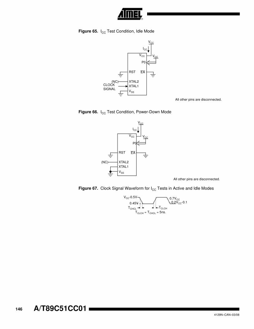
146 A/T89C51CC014129N–CAN–03/08
Figure 65. ICC Test Condition, Idle Mode
Figure 66. ICC Test Condition, Power-Down Mode
Figure 67. Clock Signal Waveform for ICC Tests in Active and Idle Modes
RST EA
XTAL2
XTAL1
VSS
VCC
VCC
ICC
(NC)
P0
VCC
All other pins are disconnected.
CLOCK
SIGNAL
RST EA
XTAL2
XTAL1
VSS
VCC
VCC
ICC
(NC)
P0
VCC
All other pins are disconnected.
VCC-0.5V
0.45V
0.7VCC
0.2VCC-0.1
TCLCHTCHCL
TCLCH = TCHCL = 5ns.

147
A/T89C51CC01
4129N–CAN–03/08
DC Parameters for A/D Converter
Notes: 1. Typicals are based on a limited number of samples and are not guaranteed.
2. With ADC enabled.
AC Parameters
Explanation of the AC
Symbols
Each timing symbol has 5 characters. The first character is always a “T” (stands for
time). The other characters, depending on their positions, stand for the name of a signal
or the logical status of that signal. The following is a list of all the characters and what
they stand for.
Example: TAVLL = Time for Address Valid to ALE Low.
TLLPL = Time for ALE Low to PSEN Low.
TA = -40°C to +85°C; VSS = 0V; VCC = 5V ±10%; F = 0 to 40 MHz.
TA = -40°C to +85°C; VSS = 0V; VCC = 5V ± 10%.
(Load Capacitance for port 0, ALE and PSEN = 60 pF; Load Capacitance for all other
outputs = 60 pF.)
Table 123, Table 126 and Table 129 give the description of each AC symbols.
Table 124, Table 128 and Table 130 give for each range the AC parameter.
Table 125, Table 128 and Table 131 give the frequency derating formula of the AC
parameter for each speed range description. To calculate each AC symbols: Take the x
value and use this value in the formula.
Example: TLLIV and 20 MHz, Standard clock.
x = 30 ns
T = 50 ns
TCCIV = 4T - x = 170 ns
Table 122. DC Parameters for AD Converter in Precision Conversion
Symbol Parameter Min Typ(1) Max Unit Test Conditions
AVin Analog input voltage Vss- 0.2 Vref + 0.2 V
Rref(2) Resistance between Vref and Vss 12 16 24 kΩ
Varef Reference voltage 2.40 3.00 V
Cai Analog input Capacitance 60 pF During sampling
Rai Analog input Resistor 400 Ω During sampling
INL Integral non linearity 1 2 lsb
DNL Differential non linearity 0.5 1 lsb
OE Offset error -2 2 lsb

148 A/T89C51CC014129N–CAN–03/08
External Program Memory
Characteristics
Table 123. Symbol Description
Table 124. AC Parameters for a Fix Clock (F = 40 MHz)
Symbol Parameter
T Oscillator clock period
TLHLL ALE pulse width
TAVLL Address Valid to ALE
TLLAX Address Hold After ALE
TLLIV ALE to Valid Instruction In
TLLPL ALE to PSEN
TPLPH PSEN Pulse Width
TPLIV PSEN to Valid Instruction In
TPXIX Input Instruction Hold After PSEN
TPXIZ Input Instruction Float After PSEN
TAVIV Address to Valid Instruction In
TPLAZ PSEN Low to Address Float
Symbol Min Max Units
T 25 ns
TLHLL 40 ns
TAVLL 10 ns
TLLAX 10 ns
TLLIV 70 ns
TLLPL 15 ns
TPLPH 55 ns
TPLIV 35 ns
TPXIX 0 ns
TPXIZ 18 ns
TAVIV 85 ns
TPLAZ 10 ns

149
A/T89C51CC01
4129N–CAN–03/08
Table 125. AC Parameters for a Variable Clock
External Program Memory Read Cycle
Symbol Type
Standard
Clock X2 Clock X parameter Units
TLHLL Min 2 T - x T - x 10 ns
TAVLL Min T - x 0.5 T - x 15 ns
TLLAX Min T - x 0.5 T - x 15 ns
TLLIV Max 4 T - x 2 T - x 30 ns
TLLPL Min T - x 0.5 T - x 10 ns
TPLPH Min 3 T - x 1.5 T - x 20 ns
TPLIV Max 3 T - x 1.5 T - x 40 ns
TPXIX Min x x 0 ns
TPXIZ Max T - x 0.5 T - x 7 ns
TAVIV Max 5 T - x 2.5 T - x 40 ns
TPLAZ Max x x 10 ns
TPLIVTPLAZ
ALE
PSEN
PORT 0
PORT 2
A0-A7A0-A7 INSTR ININSTR IN INSTR IN
ADDRESSOR SFR-P2 ADDRESS A8-A15ADDRESS A8-A15
12 TCLCL
TAVIV
TLHLL
TAVLL
TLLIV
TLLPL
TPLPH
TPXAV
TPXIX
TPXIZTLLAX
150 A/T89C51CC014129N–CAN–03/08
External Data Memory
Characteristics
Table 126. Symbol Description
Table 127. AC Parameters for a Variable Clock (F=40MHz)
Symbol Parameter
TRLRH RD Pulse Width
TWLWH WR Pulse Width
TRLDV RD to Valid Data In
TRHDX Data Hold After RD
TRHDZ Data Float After RD
TLLDV ALE to Valid Data In
TAVDV Address to Valid Data In
TLLWL ALE to WR or RD
TAVWL Address to WR or RD
TQVWX Data Valid to WR Transition
TQVWH Data set-up to WR High
TWHQX Data Hold After WR
TRLAZ RD Low to Address Float
TWHLH RD or WR High to ALE high
Symbol Min Max Units
TRLRH 130 ns
TWLWH 130 ns
TRLDV 100 ns
TRHDX 0 ns
TRHDZ 30 ns
TLLDV 160 ns
TAVDV 165 ns
TLLWL 50 100 ns
TAVWL 75 ns
TQVWX 10 ns
TQVWH 160 ns
TWHQX 15 ns
TRLAZ 0 ns
TWHLH 10 40 ns
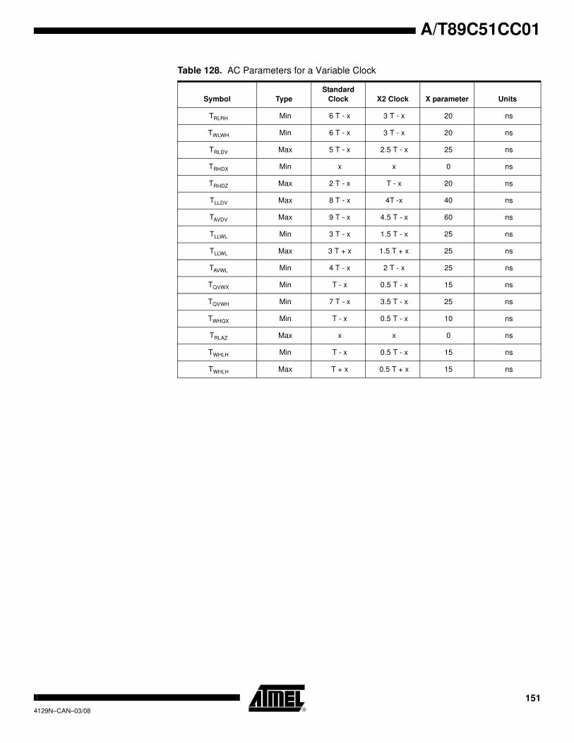
151
A/T89C51CC01
4129N–CAN–03/08
Table 128. AC Parameters for a Variable Clock
Symbol Type
Standard
Clock X2 Clock X parameter Units
TRLRH Min 6 T - x 3 T - x 20 ns
TWLWH Min 6 T - x 3 T - x 20 ns
TRLDV Max 5 T - x 2.5 T - x 25 ns
TRHDX Min x x 0 ns
TRHDZ Max 2 T - x T - x 20 ns
TLLDV Max 8 T - x 4T -x 40 ns
TAVDV Max 9 T - x 4.5 T - x 60 ns
TLLWL Min 3 T - x 1.5 T - x 25 ns
TLLWL Max 3 T + x 1.5 T + x 25 ns
TAVWL Min 4 T - x 2 T - x 25 ns
TQVWX Min T - x 0.5 T - x 15 ns
TQVWH Min 7 T - x 3.5 T - x 25 ns
TWHQX Min T - x 0.5 T - x 10 ns
TRLAZ Max x x 0 ns
TWHLH Min T - x 0.5 T - x 15 ns
TWHLH Max T + x 0.5 T + x 15 ns

152 A/T89C51CC014129N–CAN–03/08
External Data Memory Write Cycle
External Data Memory Read Cycle
Serial Port Timing – Shift Register Mode
Table 129. Symbol Description (F = 40 MHz)
TQVWHTLLAX
ALE
PSEN
WR
PORT 0
PORT 2
A0-A7 DATA OUT
ADDRESSOR SFR-P2
TAVWL
TLLWL
TQVWX
ADDRESS A8-A15 OR SFR P2
TWHQX
TWHLH
TWLWH
ALE
PSEN
RD
PORT 0
PORT 2
A0-A7 DATA IN
ADDRESSOR SFR-P2
TAVWL
TLLWL
TRLAZ
ADDRESS A8-A15 OR SFR P2
TRHDZ
TWHLH
TRLRH
TLLDV
TRHDXTLLAX
TAVDV
Symbol Parameter
TXLXL Serial port clock cycle time
TQVHX Output data set-up to clock rising edge
TXHQX Output data hold after clock rising edge
TXHDX Input data hold after clock rising edge
TXHDV Clock rising edge to input data valid

153
A/T89C51CC01
4129N–CAN–03/08
Table 130. AC Parameters for a Fix Clock (F = 40 MHz)
Table 131. AC Parameters for a Variable Clock
Shift Register Timing
Waveforms
External Clock Drive
Characteristics (XTAL1)
Table 132. AC Parameters
Symbol Min Max Units
TXLXL 300 ns
TQVHX 200 ns
TXHQX 30 ns
TXHDX 0 ns
TXHDV 117 ns
Symbol Type
Standard
Clock X2 Clock
X parameter
for -M range Units
TXLXL Min 12 T 6 T ns
TQVHX Min 10 T - x 5 T - x 50 ns
TXHQX Min 2 T - x T - x 20 ns
TXHDX Min x x 0 ns
TXHDV Max 10 T - x 5 T- x 133 ns
VALID VALID VALID VALID VALIDVALIDINPUT DATA VALID
0 1 2 3 4 5 6 87
ALE
CLOCK
OUTPUT DATA
WRITE to SBUF
CLEAR RI
TXLXL
TQVXHTXHQX
TXHDV
TXHDX SET TI
SET RI
INSTRUCTION
0 1 2 3 4 5 6 7
VALID
Symbol Parameter Min Max Units
TCLCL Oscillator Period 25 ns
TCHCX High Time 5 ns
TCLCX Low Time 5 ns
TCLCH Rise Time 5 ns
TCHCL Fall Time 5 ns
TCHCX/TCLCX Cyclic ratio in X2 mode 40 60 %
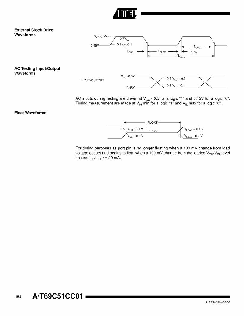
154 A/T89C51CC014129N–CAN–03/08
External Clock Drive
Waveforms
AC Testing Input/Output
Waveforms
AC inputs during testing are driven at VCC - 0.5 for a logic “1” and 0.45V for a logic “0”.
Timing measurement are made at VIH min for a logic “1” and VIL max for a logic “0”.
Float Waveforms
For timing purposes as port pin is no longer floating when a 100 mV change from load
voltage occurs and begins to float when a 100 mV change from the loaded VOH/VOL level
occurs. IOL/IOH ≥ ± 20 mA.
VCC-0.5V
0.45V
0.7VCC
0.2VCC-0.1
TCHCL TCLCX
TCLCL
TCLCH
TCHCX
INPUT/OUTPUT0.2 VCC + 0.9
0.2 VCC - 0.1
VCC -0.5V
0.45V
FLOAT
VOH - 0.1 V
VOL + 0.1 V
VLOADVLOAD + 0.1 V
VLOAD - 0.1 V

155
A/T89C51CC01
4129N–CAN–03/08
Clock Waveforms Valid in normal clock mode. In X2 mode XTAL2 must be changed to XTAL2/2.
This diagram indicates when signals are clocked internally. The time it takes the signals to propagate to the pins, however,
ranges from 25 to 125 ns. This propagation delay is dependent on variables such as temperature and pin loading. Propaga-
tion also varies from output to output and component. Typically though (TA=25°C fully loaded) RD and WR propagation
delays are approximately 50ns. The other signals are typically 85 ns. Propagation delays are incorporated in the AC
specifications.
DATA PCL OUT DATA PCL OUT DATA PCL OUT SAMPLED SAMPLED SAMPLED
STATE4 STATE5 STATE6 STATE1 STATE2 STATE3 STATE4 STATE5
P1 P2 P1 P2 P1 P2 P1 P2 P1 P2 P1 P2 P1 P2 P1 P2
FLOAT FLOAT FLOAT
THESE SIGNALS ARE NOT ACTIVATED DURING THEEXECUTION OF A MOVX INSTRUCTION
INDICATES ADDRESS TRANSITIONS
EXTERNAL PROGRAM MEMORY FETCH
FLOAT
DATASAMPLED
DPL OR Rt OUT
INDICATES DPH OR P2 SFR TO PCH TRANSITION
PCL OUT (IF PROGRAMMEMORY IS EXTERNAL)
PCL OUT (EVEN IF PROGRAMMEMORY IS INTERNAL)
PCL OUT (IF PROGRAMMEMORY IS EXTERNAL)
OLD DATA NEW DATA
P0 PINS SAMPLED
P1, P2, P3 PINS SAMPLED P1, P2, P3 PINS SAMPLED
P0 PINS SAMPLED
RXD SAMPLED
INTERNALCLOCK
XTAL2
ALE
PSEN
P0
P2 (EXT)
READ CYCLE
WRITE CYCLE
RD
P0
P2
WR
PORT OPERATION
MOV PORT SRC
MOV DEST P0
MOV DEST PORT (P1. P2. P3)(INCLUDES INTO. INT1. TO T1)
SERIAL PORT SHIFT CLOCK
TXD (MODE 0)
DATA OUT
DPL OR Rt OUT
INDICATES DPH OR P2 SFR TO PCH TRANSITION
P0
P2
RXD SAMPLED

156 A/T89C51CC014129N–CAN–03/08
Flash/EEPROM Memory Table 133. Timing Symbol Definitions
Table 134. Memory AC Timing
VDD = 3V to 5.5V, TA = -40 to +85°C
Figure 68. Flash Memory – ISP Waveforms
Figure 69. Flash Memory – Internal Busy Waveforms
A/D Converter Table 135. AC Parameters for A/D Conversion
Signals Conditions
S (Hardware
condition)PSEN#,EA L Low
R RST V Valid
B FBUSY flag X No Longer Valid
Symbol Parameter Min Typ Max Unit
TSVRL Input PSEN# Valid to RST Edge 50 ns
TRLSX Input PSEN# Hold after RST Edge 50 ns
TBHBL
Flash/EEPROM Internal Busy
(Programming) Time (2.7 V)14 21 ms
Flash/EEPROM Internal Busy
(Programming) Time (3.3 V)10 15 ms
NFCY
Number of Flash/EEPROM Erase/Write
Cycles100 000 cycles
TFDR Flash/EEPROM Data Retention Time 10 years
RST
TSVRL
PSEN#1
TRLSX
FBUSY bitTBHBL
Symbol Parameter Min Typ Max Unit
TSETUP 4 µs
ADC Clock Frequency 700 KHz

157
A/T89C51CC01
4129N–CAN–03/08
Ordering Information
• Factory default programming for T89C51CC01CA-xxxx is bootloader CAN and
HSB=BBh
– . X1 mode
– . BLJB = 0; jump to Bootloader
– . LB2 = 0 Security Level 4
• Factory default programming for T89C51CC01UA-xxxx is bootloader UART and
HSB=BBh
– . X1 mode
– . BLJB = 0; jump to Bootloader
– . LB2 = 0 Security Level 4
Note: Customer can change these modes by re-programming with a parallel programmer, this
can be done by an Atmel distributor.
Table 136. Possible Order Entries
Part Number Boot Loader Temperature Range Package Packing Product Marking
T89C51CC01UA-7CTIM
OBSOLETE
T89C51CC01UA-RLTIM
T89C51CC01UA-SLSIM
T89C51CC01CA-7CTIM
T89C51CC01CA-RLTIM
T89C51CC01CA-SLSIM
AT89C51CC01UA-RLTUM UART Industrial & Green VQFP44 Tray 89C51CC01UA-UM
AT89C51CC01UA-SLSUM UART Industrial & Green PLCC44 Stick 89C51CC01UA-UM
AT89C51CC01CA-RLTUM CAN Industrial & Green VQFP44 Tray 89C51CC01CA-UM
AT89C51CC01CA-SLSUM CAN Industrial & Green PLCC44 Stick 89C51CC01CA-UM

158 A/T89C51CC014129N–CAN–03/08
Package Drawings
VQFP44

159
A/T89C51CC01
4129N–CAN–03/08
STANDARD NOTES FOR PQFP/ VQFP / TQFP / DQFP
1/ CONTROLLING DIMENSIONS : INCHES
2/ ALL DIMENSIONING AND TOLERANCING CONFORM TO ANSI Y 14.5M -1982.
3/ "D1 AND E1" DIMENSIONS DO NOT INCLUDE MOLD PROTUSIONS.
MOLD PROTUSIONS SHALL NOT EXCEED 0.25 mm (0.010 INCH).
THE TOP PACKAGE BODY SIZE MAY BE SMALLER THAN THE BOTTOM
PACKAGE BODY SIZE BY AS MUCH AS 0.15 mm.
4/ DATUM PLANE "H" LOCATED AT MOLD PARTING LINE AND
COINCIDENT WITH LEAD, WHERE LEAD EXITS PLASTIC BODY AT
BOTTOM OF PARTING LINE.
5/ DATUM "A" AND "D" TO BE DETERMINED AT DATUM PLANE H.
6/ DIMENSION " f " DOES NOT INCLUDE DAMBAR PROTUSION ALLOWABLE
DAMBAR PROTUSION SHALL BE 0.08mm/.003" TOTAL IN EXCESS OF THE
" f " DIMENSION AT MAXIMUM MATERIAL CONDITION .
DAMBAR CANNOT BE LOCATED ON THE LOWER RADIUS OR THE FOOT.
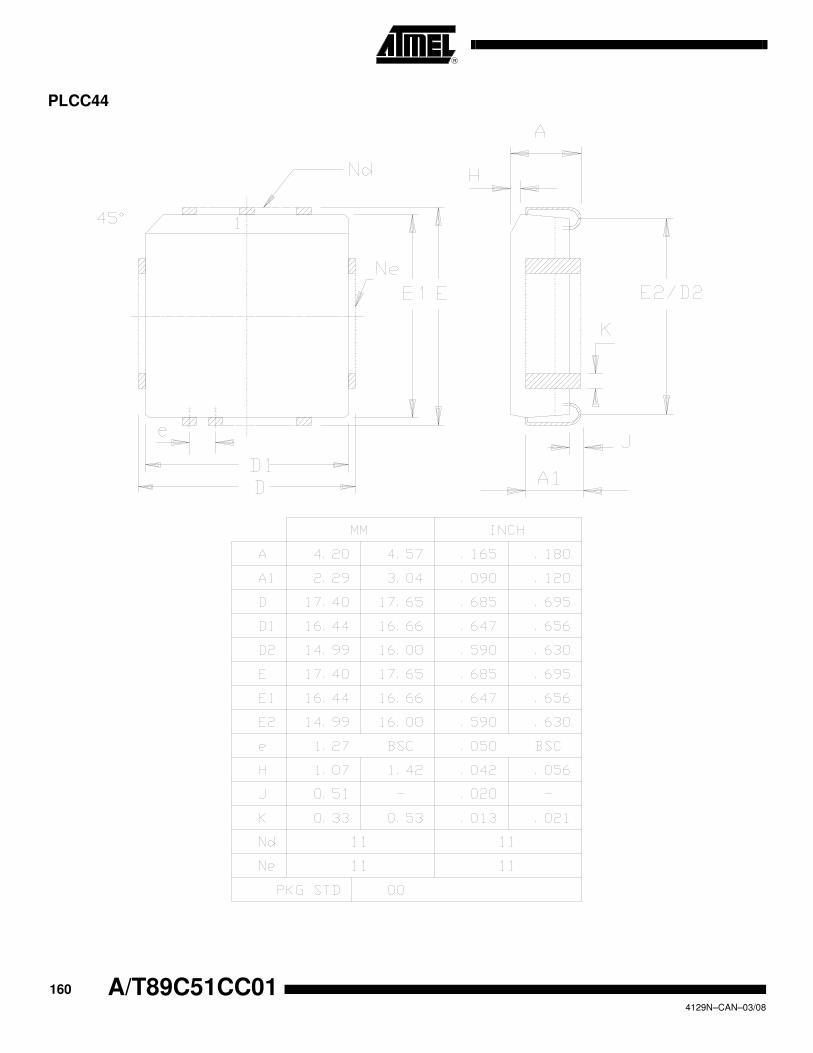
160 A/T89C51CC014129N–CAN–03/08
PLCC44

161
A/T89C51CC01
4129N–CAN–03/08
STANDARD NOTES FOR PLCC
1/ CONTROLLING DIMENSIONS : INCHES
2/ DIMENSIONING AND TOLERANCING PER ANSI Y 14.5M - 1982.
3/ "D" AND "E1" DIMENSIONS DO NOT INCLUDE MOLD FLASH OR PROTUSIONS.MOLD FLASH OR PROTUSIONS SHALL NOT EXCEED 0.20 mm (.008 INCH) PER
SIDE.

162 A/T89C51CC014129N–CAN–03/08
Datasheet Change
Log for T89C51CC01
Changes from 4129F - 11/02 to 4129G - 04/03
1. Changed the endurance of Flash to 100, 000 Write/Erase cycles.
2. Added note on Flash retention formula for VIH1, in Section "DC Parameters for
Standard Voltage", page 144.
Changes from 4129G - 04/03 to 4129H - 10/03
1. Updated “Electrical Characteristics” on page 144.
2. Corrected Figure 46 on page 84.
Changes from 4129H - 10/03 to 4129I - 12/03
1. Correction in Registers CPA and CPS0.
2. Added note regarding PSEN during power On see Section “Hardware Boot Pro-
cess”, page 48.
Changes from 4129I - 12/03 to 4129J - 08/04
1. Figure clock-out mode modified see, Figure 37 on page 67.
2. Added explanation on the CAN protocol, see Section “CAN Controller”, page 75.
3. Corrected error in Table 53 on page 72, (1.25ms to 1.25s) for Time-out
Computation.
Changes from 4129J - 08/04 to 4129K 01/05
1. Minor corrections throughout the document.
2. Clarification to Mode Switching Waveforms diagram. See page 16.
Changes from 4129K 01/05 to 4129L 08/05
1. Added green product ordering information.
Changes from 4129L 08/05 to 4129M 02/08
1. Removed non-green packages from ordering information.
Changes from 4129M 02/08 to 4129N 03/08
1. Removed CA-BGA package offering from ordering information.
2. Updated package drawings.

Table of Contents
i
Table of Contents
Features ................................................................................................. 1
Description ............................................................................................ 2
Block Diagram ....................................................................................... 2
Pin Configuration .................................................................................. 3
I/O Configurations ................................................................................................ 4
Port 1, Port 3 and Port 4....................................................................................... 4
Port 0 and Port 2 .................................................................................................. 4
Read-Modify-Write Instructions ............................................................................ 5
Quasi-Bidirectional Port Operation ....................................................................... 6
SFR Mapping ......................................................................................... 8
Clock .................................................................................................... 14
Description ......................................................................................................... 14
Register ............................................................................................................... 17
Power Management ............................................................................ 18
Reset Pin............................................................................................................ 18
At Power-up (Cold Reset) .................................................................................. 18
Reset Recommendation to Prevent Flash Corruption........................................ 19
Idle Mode............................................................................................................ 19
Power-down Mode ............................................................................................. 20
Registers ............................................................................................................ 22
Data Memory ....................................................................................... 23
Internal Space ..................................................................................................... 24
External Space ................................................................................................... 25
Dual Data Pointer ................................................................................................ 27
Registers ............................................................................................................ 28
EEPROM Data Memory ....................................................................... 30
Write Data in the Column Latches...................................................................... 30
Programming...................................................................................................... 30
Read Data .......................................................................................................... 30
Examples............................................................................................................ 31
Registers ............................................................................................................ 32

ii
Program/Code Memory ...................................................................... 33
External Code Memory Access ........................................................................... 34
Flash Memory Architecture ................................................................................ 35
Overview of FM0 Operations.............................................................................. 37
Registers ............................................................................................................ 43
Operation Cross Memory Access ..................................................... 44
Sharing Instructions ........................................................................... 45
In-System Programming (ISP) ........................................................... 47
Flash Programming and Erasure ....................................................................... 47
Boot Process ...................................................................................................... 48
Application Programming Interface .................................................................... 49
XROW Bytes ...................................................................................................... 49
Hardware Security Byte...................................................................................... 50
Serial I/O Port ...................................................................................... 51
Framing Error Detection .................................................................................... 51
Automatic Address Recognition ......................................................................... 52
Given Address..................................................................................................... 53
Broadcast Address ............................................................................................. 53
Registers ............................................................................................................ 54
Timers/Counters ................................................................................. 57
Timer/Counter Operations.................................................................................. 57
Timer 0 ............................................................................................................... 57
Timer 1 ................................................................................................................ 60
Interrupt .............................................................................................................. 60
Registers ............................................................................................................ 62
Timer 2 ................................................................................................. 66
Auto-Reload Mode ............................................................................................ 66
Programmable Clock-Output .............................................................................. 67
Registers ............................................................................................................ 68
Watchdog Timer .................................................................................. 71
Watchdog Programming...................................................................................... 72
Watchdog Timer During Power-down Mode and Idle.......................................... 73
CAN Controller .................................................................................... 75
CAN Protocol...................................................................................................... 75

Table of Contents
iii
CAN Controller Description ................................................................................ 79
CAN Controller Mailbox and Registers Organization ......................................... 80
CAN Controller Management ............................................................................. 82
IT CAN Management........................................................................................... 84
Bit Timing and Baud Rate .................................................................................. 86
Fault Confinement .............................................................................................. 88
Acceptance Filter................................................................................................ 89
Data and Remote Frame.................................................................................... 90
Time Trigger Communication (TTC) and Message Stamping ............................ 91
CAN Autobaud and Listening Mode ................................................................... 92
Routines Examples ............................................................................................ 92
CAN SFR’s ......................................................................................................... 95
Registers ............................................................................................................ 96
Programmable Counter Array (PCA) ............................................... 118
PCA Timer ........................................................................................................ 118
PCA Modules ................................................................................................... 119
PCA Interrupt.................................................................................................... 120
PCA Capture Mode .......................................................................................... 120
16-bit Software Timer Mode ............................................................................. 121
High Speed Output Mode.................................................................................. 122
Pulse Width Modulator Mode ........................................................................... 122
PCA Watchdog Timer....................................................................................... 123
PCA Registers ................................................................................................... 124
Analog-to-Digital Converter (ADC) .................................................. 129
Features ........................................................................................................... 129
ADC Port 1 I/O Functions................................................................................. 129
VAREF ............................................................................................................. 129
ADC Converter Operation ................................................................................ 131
Voltage Conversion .......................................................................................... 131
Clock Selection................................................................................................. 131
ADC Standby Mode.......................................................................................... 132
IT ADC Management........................................................................................ 132
Routines examples........................................................................................... 132
Registers ........................................................................................................... 134
Interrupt System ............................................................................... 136
Introduction....................................................................................................... 136
Registers .......................................................................................................... 138
Electrical Characteristics ................................................................. 144
iv
Absolute Maximum Ratings ............................................................................. 144
DC Parameters for Standard Voltage............................................................... 144
DC Parameters for A/D Converter.................................................................... 147
AC Parameters................................................................................................. 147
Ordering Information ........................................................................ 157
Package Drawings ............................................................................ 158
VQFP44............................................................................................................ 158
PLCC44............................................................................................................. 160
Datasheet Change Log for T89C51CC01 ........................................ 162
Changes from 4129F - 11/02 to 4129G - 04/03 ............................................... 162
Changes from 4129G - 04/03 to 4129H - 10/03 ............................................... 162
Changes from 4129H - 10/03 to 4129I - 12/03 ................................................. 162
Changes from 4129I - 12/03 to 4129J - 08/04.................................................. 162
Changes from 4129J - 08/04 to 4129K 01/05 .................................................. 162
Changes from 4129K 01/05 to 4129L 08/05 .................................................... 162
Changes from 4129L 08/05 to 4129M 02/08.................................................... 162
Changes from 4129M 02/08 to 4129N 03/08 ................................................... 162
Table of Contents ................................................................................... i

Printed on recycled paper.
Disclaimer: Atmel Corporation makes no warranty for the use of its products, other than those expressly contained in the Company’s standardwarranty which is detailed in Atmel’s Terms and Conditions located on the Company’s web site. The Company assumes no responsibility for anyerrors which may appear in this document, reserves the right to change devices or specifications detailed herein at any time without notice, anddoes not make any commitment to update the information contained herein. No licenses to patents or other intellectual property of Atmel aregranted by the Company in connection with the sale of Atmel products, expressly or by implication. Atmel’s products are not authorized for useas critical components in life support devices or systems.
Atmel Corporation Atmel Operations
2325 Orchard Parkway
San Jose, CA 95131, USA
Tel: 1(408) 441-0311
Fax: 1(408) 487-2600
Regional Headquarters
Europe
Atmel Sarl
Route des Arsenaux 41
Case Postale 80
CH-1705 Fribourg
Switzerland
Tel: (41) 26-426-5555
Fax: (41) 26-426-5500
Asia
Room 1219
Chinachem Golden Plaza
77 Mody Road Tsimshatsui
East Kowloon
Hong Kong
Tel: (852) 2721-9778
Fax: (852) 2722-1369
Japan
9F, Tonetsu Shinkawa Bldg.
1-24-8 Shinkawa
Chuo-ku, Tokyo 104-0033
Japan
Tel: (81) 3-3523-3551
Fax: (81) 3-3523-7581
Memory
2325 Orchard Parkway
San Jose, CA 95131, USA
Tel: 1(408) 441-0311
Fax: 1(408) 436-4314
Microcontrollers
2325 Orchard Parkway
San Jose, CA 95131, USA
Tel: 1(408) 441-0311
Fax: 1(408) 436-4314
La Chantrerie
BP 70602
44306 Nantes Cedex 3, France
Tel: (33) 2-40-18-18-18
Fax: (33) 2-40-18-19-60
ASIC/ASSP/Smart Cards
Zone Industrielle
13106 Rousset Cedex, France
Tel: (33) 4-42-53-60-00
Fax: (33) 4-42-53-60-01
1150 East Cheyenne Mtn. Blvd.
Colorado Springs, CO 80906, USA
Tel: 1(719) 576-3300
Fax: 1(719) 540-1759
Scottish Enterprise Technology Park
Maxwell Building
East Kilbride G75 0QR, Scotland
Tel: (44) 1355-803-000
Fax: (44) 1355-242-743
RF/Automotive
Theresienstrasse 2
Postfach 3535
74025 Heilbronn, Germany
Tel: (49) 71-31-67-0
Fax: (49) 71-31-67-2340
1150 East Cheyenne Mtn. Blvd.
Colorado Springs, CO 80906, USA
Tel: 1(719) 576-3300
Fax: 1(719) 540-1759
Biometrics/Imaging/Hi-Rel MPU/
High Speed Converters/RF Datacom
Avenue de Rochepleine
BP 123
38521 Saint-Egreve Cedex, France
Tel: (33) 4-76-58-30-00
Fax: (33) 4-76-58-34-80
Literature Requests
www.atmel.com/literature
4129N–CAN–03/08
© Atmel Corporation 2008. All rights reserved. Atmel® and combinations thereof are the registered trademarks of Atmel Corporation or its
subsidiaries. Other terms and product names may be the trademarks of others.