architectural power management for battery lifetime optimization in portable systems department of...
Post on 19-Dec-2015
213 views
TRANSCRIPT

Architectural Power Management for Battery Lifetime Optimization in Portable Systems
Department of Electrical and Computer Engineering Auburn University, Auburn, AL 36849, USA
1
Manish Kulkarni Vishwani D. Agrawal
Manish Kulkarni and Vishwani AgrawalVLSI Design and Test Symposium, July 2011

Outline• Recent work and publications• Summary of tutorial on battery modeling and efficiency (VDAT’10)• Energy source optimization methods• Functional management• Hardware modes for power reduction• Power gating example• Power savings in components of a processor• SLOP implementation in a pipeline• Power and energy savings• Conclusion • References
2Manish Kulkarni and Vishwani AgrawalVLSI Design and Test Symposium, July 2011

Recent Work and Publications Khushaboo Sheth, “A Hardware-Software Processor Architecture using
Pipeline Stalls for Leakage Power Management,” Master’s Thesis, Auburn University, ECE Dept.,Dec. 2008.
M. Kulkarni and V. D. Agrawal, “Matching Power Source to Electronic System: A Tutorial on Battery Simulation,” Proc. VLSI Design and Test Symposium, July 2010.
M. Kulkarni, “Energy Source Lifetime Optimization for a Digital System through Power Management,” Master’s Thesis, Auburn University, ECE Dept., Dec. 2010.
M. Kulkarni and V. D. Agrawal, “Energy Source Lifetime Optimization for a Digital System through Power Management,” Proc. 43rd IEEE Southeastern Symp. System Theory, Mar. 2011, pp. 75–80.
M. Kulkarni, K. Sheth, and V. D. Agrawal, “Architectural Power Management for High Leakage Technologies,” Proc. 43rd IEEE Southeastern Symp. System Theory, Mar. 2011, pp. 69–74.
3Manish Kulkarni and Vishwani AgrawalVLSI Design and Test Symposium, July 2011

An Electronic System Model for Dynamic Voltage and Frequency Scaling (DVFS)
VLSI Design and Test Symposium, July 2011 Manish Kulkarni and Vishwani Agrawal 4
DC – DCVoltage
Converter [9]
Electronic System
4.2 V to 3.5 V Lithium- ion
BatteryDecoupling Capacitor
VDD
GND
• Electronic systems are not always required to be in highest performance mode
• Frequency and voltage can be varied• Multi-voltage domains can be created which can use DVFS or
power shutdown

VLSI Design and Test Symposium, July 2011 5
Battery Simulation ModelLithium-ion battery, unit cell capacity: N = 1 (400mAh)Battery sizes, N = 2 (800mAh), N = 3 (1.2Ah), etc.
[3] M. Chen and G. A. Rincón-Mora, “Accurate Electrical Battery Model Capable of Predicting Runtime and I-V Performance,” IEEE Transactions on Energy Conversion, vol. 21, no. 2, pp. 504–511, June 2006.
Manish Kulkarni and Vishwani Agrawal

0.00 0.20 0.40 0.60 0.80 1.00 1.200.00E+00
2.00E+11
4.00E+11
6.00E+11
8.00E+11
1.00E+12
1.20E+12
1.40E+12
1.60E+12
1.80E+12
Ideal Battery
Simulated Battery
VDD (Volts)
Num
ber o
f Cyc
les p
er R
echa
rge
VLSI Design and Test Symposium, July 2011 6
Higher Circuit Speed,Lower Battery Efficiency
Simulation of 70-Million Gate SOC With 400mAh Battery
0.098 0.560 3.860 23.00 88.00 199.0 325.0 446.0 557.0 657.0 (MHz) Manish Kulkarni and Vishwani Agrawal
DVFS
619 Giga Cyclesor
50 minutes
Higher Battery Lifetime,Lower Circuit Speed

Summary of Battery Tutorial
Battery sizeVDD = 0.6V, 200MHz VDD = 0.3V*, 3.86MHz
Effici.%
LifetimeEffici.
%
Lifetime
N mAh x103 seconds
X10 9 cycles
x103 seconds
X10 9 cycles
1 400 98 3 619 100+ 430 16604 1600 100+ 12.7 2540 100+ 1717 6630
VLSI Design and Test Symposium, July 2011 7
> two-times
1. Battery size should match the current need and satisfy the lifetime requirement of the system:a) Undersize battery has poor efficiency.b) Oversize battery is bulky and expensive.
2. Minimum energy mode can significantly increase battery lifetime.3. A practical case of application where a miniature (undersized) battery
is required is discussed in [9].* Operation of circuits in sub-threshold voltage range (below 200 mV) have been verified [12][13]
Manish Kulkarni and Vishwani Agrawal

8
Clock Rate Management
Functional Management
Voltage Management
Energy Source Optimization Methods
• Dynamic Voltage Management • Multi-Voltage design
• Dynamic Frequency Management • Retiming
• Fetch Throttling• Dynamic Task Scheduling • Instruction Slowdown• Low Power solutions to common
operations e.g. Low Power FSMs, Bus Encoding etc
• Dynamic Voltage and Frequency Scaling (DVFS)
Clock Rate Management
Functional Management
Voltage Management
• Parallel and Multi-core Architectures
Manish Kulkarni and Vishwani AgrawalVLSI Design and Test Symposium, July 2011

• Low Power Design Techniques– Dynamic voltage and frequency scaling (DVFS)
• Scale Voltage and Frequency depending on throughput requirement.• Use of multi-voltage domains and multiple clocks.
– Frequency scaling at constant voltage (Clock Slowdown)• Increase in leakage energy in high leakage technologies• Voltage scaling has a limit.
22nm bulk CMOS, Vnom = 0.8 V, Vth = 0.32 V [4]• High power delivered at low voltages causes higher IR drops in
power rails in chips.• Proposed method
– Instruction slowdown [8]• Voltage and Frequency are kept constant.• Specialized instructions called Slowdown for LOw Power (SLOP) are
inserted in the pipeline.• Additional control is provided in the data path to execute Clock
Gating (CG) or Power Gating (PG) of idle units in the pipeline.
9
Functional Management
Manish Kulkarni and Vishwani AgrawalVLSI Design and Test Symposium, July 2011

Hardware Modes for Power Reduction
• Power gating (PG)– Used primarily for combinational logic– Header or footer switches to reduce leakage
power • Clock gating (CG)
– Used for flip flops and registers– Reduces switching activity; data is retained – No need for state retention
• Drowsy mode– Used for caches, memories and register files– Memory cells are put in low voltage mode– Address decoders and sense amplifiers in
power gated mode10
Figure: Power Gating
Figure: Clock Gating
LogicBlock
Header SwitchSleep
Virtual Supply
Manish Kulkarni and Vishwani AgrawalVLSI Design and Test Symposium, July 2011
11
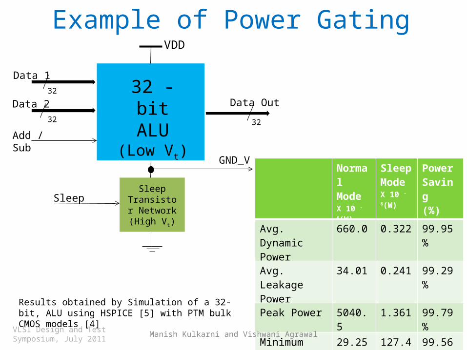
Example of Power Gating
Data 1
Data 2
Add / Sub
Data Out32
32 32
32 - bitALU
(Low Vt)
Sleep Transistor Network(High Vt)
VDD
Sleep
GND_V NormalModeX 10 -6(W)
SleepMode X 10 -6(W)
Power Saving (%)
Avg. Dynamic Power
660.0 0.322 99.95 %
Avg. Leakage Power
34.01 0.241 99.29 %
Peak Power 5040.5 1.361 99.79 %
Minimum Power
29.254 127.4 99.56 %Results obtained by Simulation of a 32-bit, ALU using HSPICE [5] with PTM bulk CMOS models [4]
Manish Kulkarni and Vishwani AgrawalVLSI Design and Test Symposium, July 2011

12
Hardware block Power mode during SLOP
Power consumed (%)*
Dynamic Static
PC CG 25 100
Instruction and Data cache Drowsy 25 25
Register file CG 30 100
Forwarding, hazard unit PG ≈0 ≈0
ALU, FPU, comparators, branch decoders
PG ≈0 ≈0
Control Unit Normal 100 100
Pipeline registers CG 50 100
Multiplexers, other adders PG ≈0 ≈0
*Normal mode power consumption for each block is 100%PG – Power gating, CG – Clock gating
Power Savings in Processor Blocks
Manish Kulkarni and Vishwani AgrawalVLSI Design and Test Symposium, July 2011

13
CC1 CC2 CC3 CC4 CC5 CC6 CC7
Normal Mode Operation
LW $8, 0($7)
ADD $9, $8, $2
SW $9, 0($7)
Manish Kulkarni and Vishwani AgrawalVLSI Design and Test Symposium, July 2011

14
Operation With One SLOP CC1 CC2 CC3 CC4 CC5 CC6 CC7
LW $8, 0($7)
ADD $9, $8, $2
SW $9, 0($7)
SLOP
SLOP
CC8 CC9
Manish Kulkarni and Vishwani AgrawalVLSI Design and Test Symposium, July 2011

15
IF
CG
PG
Dro
wsy
ID
CG
PG
DM
Dro
wsy
PG
PG
PG
PG
EX
PG
PG
WB
PG
Manish Kulkarni and Vishwani AgrawalVLSI Design and Test Symposium, July 2011Ref. Patterson and Hennessey.

16
T
T
T
0 1 2 3 4
Inst
an
tan
eo
us
Po
we
r
0 1 2 3 4
0 1 2 3 4
SLOP
Freq. Scaling(Clock Slowdown)
Instruction Slowdown
Dynamic Power
Leakage Power
SLOP
Normal
VLSI Design and Test Symposium, July 2011 Manish Kulkarni and Vishwani Agrawal

17
Power, Energy and Lifetime Ratios• For 32 nm bulk CMOS models• Ideal Battery of 800 mAh Capacity
Power, energy and lifetimes are normalized to their values with zero SLOPs inserted, i.e., normal mode of operation.
Manish Kulkarni and Vishwani AgrawalVLSI Design and Test Symposium, July 2011

18
Battery Lifetime Improvement • For 32 nm bulk CMOS models• Battery of 800 mAh Capacity
0 1 2 3 40
0.2
0.4
0.6
0.8
1
1.2
1.4
1.6
1.8
Energy Used by Circuit
Battery Lifetime
Task completion time
Number of SLOPs
Tim
e in
Nor
mal
ized
Use
ful C
lock
Cyc
les
or
Ener
gy
Manish Kulkarni and Vishwani AgrawalVLSI Design and Test Symposium, July 2011

1. The proposed architectural power management method is demonstrated to be beneficial towards power optimization and energy source efficiency in high leakage technologies.
2. SLOP insertion method offers a unique opportunity in hardware and software management for energy efficiency. SLOPs may additionally eliminate pipeline hazards.
3. Use of SLOPs in superscalers and out-of-order processors can be further studied and analyzed.
19
Conclusion
Manish Kulkarni and Vishwani AgrawalVLSI Design and Test Symposium, July 2011

References1. M. Pedram and Q. Wu, “Design Considerations for Battery-Powered Electronics,” Proc. 36th Design Automation
Conference, June 1999, pp. 861–866.2. L. Benini, G. Castelli, A. Macii, E. Macii, M. Poncino, and R. Scarsi, “A Discrete-Time Battery Model for High-Level Power
Estimation,” Proc. Conference on Design, Automation and Test in Europe, Mar. 2000, pp. 35–41.3. M. Chen and G. A. Rincón-Mora, “Accurate Electrical Battery Model Capable of Predicting Runtime and I-V
Performance,” IEEE Transactions on Energy Conversion, vol. 21, no. 2, pp. 504–511, June 2006.4. Simulation model: 45nm bulk CMOS, predictive technology model (PTM), http://ptm.asu.edu/ 5. Simulator: Synopsys HSPICE,
www.synopsys.com/Tools/Verification/AMSVerification/CircuitSimulation/HSPICE/Documents/hspice ds.pdf
7. M. Kulkarni and V. D. Agrawal, “Matching Power Source to Electronic System: A Tutorial on Battery Simulation,” Proc. VLSI Design and Test Symposium, July 2010.
8. K. Sheth, “A Hardware-Software Processor Architecture using Pipeline Stalls for Leakage Power Management,” Master’s Thesis, Auburn University, ECE Dept., Dec. 2008.
9. M. Kulkarni, “Energy Source Lifetime Optimization for a Digital System through Power Management,” Master’s Thesis, Auburn University, ECE Dept., Dec. 2010.
10. M. Kulkarni and V. D. Agrawal, “Energy Source Lifetime Optimization for a Digital System through Power Management,” Proc. 43rd IEEE Southeastern Symp. System Theory, Mar. 2011, pp. 75–80.
11. M. Kulkarni, K. Sheth, and V. D. Agrawal, “Architectural Power Management for High Leakage Technologies,” Proc. 43rd IEEE Southeastern Symp. System Theory, Mar. 2011, pp. 69–74.
12. S. Hanson, B. Zhai, M. Seok, B. Cline, K. Zhou, M. Singhal, M. Minuth, J. Olson, L. Nazhandali, T. Austin, D. Sylvester, and D. S. Blaauw, “Performance and variability optimization strategies in a sub-200 mV, 3.5 pJ/inst, 11 nW subthreshold processor,” Symp. VLSI Circuits Digest, Jun. 2007, pp. 152–153.
13. B. Zhai, S. Hanson, D. Blaauw, and D. Sylvester, “A Variation-Tolerant Sub-200mV 6-T Subthreshold SRAM,” IEEE Journal of Solid-State Circuits, vol. 43, no. 10. pp. 2338-2348, Oct. 2008.
20Manish Kulkarni and Vishwani AgrawalVLSI Design and Test Symposium, July 2011