april 2015 volume 25 number 1 industry’s first 0.8µv noise · 4 | april 2015 : lt journal of...
TRANSCRIPT

www.l inear.com
April 2015 Volume 25 Number 1
I N T H I S I S S U E
patent-pending boost-buck
LED driver topology 8
I2C programmable
supervisors with EEPROM
12
18V buck-boost converter
with intelligent PowerPath
control delivers >2A 16
advantages of 75W boost
mode LED driver 22
how to design an isolated,
high frequency, push-pull
DC/DC converter 25
Industry’s First 0.8µVRMS Noise LDO Has 79dB Power Supply Rejection Ratio at 1MHzAmit Patel
When it comes to powering noise-sensitive analog/RF applications, low dropout (LDO) linear regulators are generally preferred over their switching counterparts. Low noise LDOs power a wide range of analog/RF designs, including frequency synthesizers (PLLs/VCOs), RF mixers and modulators, high speed and high resolution data converters (ADCs and DACs) and precision sensors. Nevertheless, these applications have reached capabilities and sensitivities that are testing the limits of conventional low noise LDOs.
For instance, in many high end VCOs, power supply noise
directly affects the VCO output phase noise (jitter). Moreover,
to meet overall system efficiency requirements, the LDO usually post-regulates the output of a relatively noisy
switching converter, so the high frequency power supply
rejection ratio (PSRR) performance of the LDO becomes
paramount. With its ultralow output noise and ultrahigh
PSRR performance, the LT®3042 can directly power some
of most noise-sensitive applications while post-regulating
the output of a switching converter, without requir-
ing bulky filtering. Table 1 compares the LT3042’s noise
performance with conventional low noise regulators.
PERFORMANCE, ROBUSTNESS & SIMPLICITY
The LT3042 is a high performance low dropout linear
regulator featuring Linear Technology’s ultralow noise and
ultrahigh PSRR architecture for powering noise-sensitive
(continued on page 4)The LT3042 brings noise-free power to high performance electronics.

2 | April 2015 : LT Journal of Analog Innovation
In this issue...
New Analog Circuit Design Book Published by Elsevier
The third volume in Linear Technology’s Analog Circuit Design book series has
been published by Elsevier/Newnes Publishers. The book, Analog Circuit Design,
Volume 3, Design Note Collection, edited by Bob Dobkin and John Hamburger, is
a compilation of applied circuit design solutions that can be used in a broad range
of applications and systems.
The book is a comprehensive collection of Linear Technology’s highly regarded
Design Notes. The Notes have been written over the past 25 years by some of the
leading lights of analog design, including Jim Williams, Bob Dobkin, Carl Nelson
and George Erdi, among many others. They serve as a framework to provide cir-
cuit design techniques for a range of analog design challenges.
The book is logically organized for easy reference. It includes an in-depth Power
Management section, including such topics as:
•Power management design
•Microprocessor power design
•Switching regulator design for step-down and boost converters, buck-boost
controllers and DC/DC controllers
•Linear regulator design
•µModule® power design
•Battery management
•Power over Ethernet
•Powering LED lighting
•Automotive and industrial power design
The Mixed Signal section spans a range of topics, including:
•Data conversion—analog-to-digital and digital-to-analog
•Data acquisition
•Communications interface design
•Instrumentation design
The Signal Conditioning section covers:
•Operational amplifier design techniques
•Special function amplifier design
•Voltage reference design
•Filter design
•Comparator design techniques
•System timing design
•RMS-to-DC conversion
Linear in the News
COVER STORY
Industry’s First 0.8µVRMS Noise LDO Has 79dB Power Supply Rejection Ratio at 1MHzAmit Patel 1
DESIGN FEATURES
Boost-Buck LED Driver Topology for Automotive LEDs Operates with Low Input and Output RippleKeith Szolusha 8
I2C Programmable Multichannel Voltage Supervisors with EEPROM Michael Petersen 12
18V Buck-Boost Converter with Intelligent PowerPath™ Control Delivers >2A at 95% Efficiency from Dual InputsEddy Wells 16
DESIGN IDEAS
What’s New with LTspice IV?Gabino Alonso 20
Can’t Find the Right Synchronous Boost LED Driver? Use a Synchronous Buck Converter Instead: Boost Mode Topology Drives 25V, 3A LEDs from 12V Keith Szolusha 22
How to Design an Isolated, High Frequency, Push-Pull DC/DC Converter Dawson Huang 25
new product briefs 30
back page circuits 32

April 2015 : LT Journal of Analog Innovation | 3
Linear in the news
The final section of the book covers
a range of topics in Wireless, RF and
Communications Design.
In his introduction to the book, Bob
Dobkin, CTO & Co-founder of Linear
Technology, states, “The teaching designs
in this Design Note Collection help bring
new designers up to speed and give expe-
rienced designers a starting point for even
more sophisticated designs. This book has
two purposes: to speed designs by present-
ing finished examples, as well as provid-
ing a teaching resource for designers.”
Bill Schweber, Contributing Editor to
EE Times Planet Analog, stated in his
review of the book, “There are so many
good circuit ideas and topologies along
with analysis of subtleties and design
issues, that anyone who is a serious
student or practitioner of the art and
reality of analog design will receive a
substantial return on time invested.”
Analog Circuit Design, Volume 3, Design
Note Collection, follows the positive
reception of the two prior books in
this series, Analog Circuit Design, A
Tutorial Guide to Applications and
Solutions, and Analog Circuit Design,
Volume 2, Immersion in the Black
Art of Analog Design, both edited
by Bob Dobkin and Jim Williams.
For more information on the book,
a video interview with Bob Dobkin
and ordering information from either
Elsevier or Amazon, visit www.linear.
com/designtools/acd_book.php
AWARDS
Technical Support Award
Linear Technology was presented with
the award for Best Technical Support
by SPDEI, the French Association of
Electronic Components Distributors
at an event in Paris in December.
EEPW Editors’ Choice Award
Linear’s LTC®2338-18 18-bit, 1Msps,
±10.24V true bipolar SAR ADC (analog-
to-digital converter) was selected for
the Best Mixed-Signal Chip Award by
the editors of Electronic Engineering &
Product World (China). Operating from
a single 5V supply, the LTC2338-18 has a
±10.24V true bipolar input range, making
it ideal for high voltage applications which
require a wide dynamic range. The fast
1Msps throughput with no cycle latency
makes the LTC2338-18 ideally suited for a
wide variety of high speed applications.
China Electronic Market Editors’ Choice Awards
Two Linear Technology products were
selected by the editors of China Electronic
Market magazine for Editors’ Choice
Awards:
•The LTC3355 20V 1A Buck DC/DC with
Integrated Supercap Charger and Backup
Regulator was chosen as the Most
Competitive Power Product for 2014.
•The LTC2323-16 Dual, 16-Bit, 5Msps
Differential Input ADC with Wide
Input Common Mode Range was
selected as the Most Competitive
ADC Product for 2014.
CONFERENCES & EVENTS
IPC & Embedded Expo 2015, Shenzhen Convention
& Exhibition Center, Shenzhen, China, April
15–17—Linear is presenting “99.999%
Reliable Wireless Sensor Network that
Uses Low Power” at 11:20 am, April 16 at
their 3rd Internet of Things Conference.
More info at en.embeddedexpo.com/
2nd Annual LTspice Users Conference, Tokyo
Conference Center, Tokyo, Japan, April 17, Halls
A & B—Mike Engelhardt, a developer of
LTspice® design tools, will make a pre-
sentation on the latest developments
regarding LTspice software. For registra-
tion and more info, visit www.ltspice.jp
Wireless Japan 2015, Tokyo Big Site, Tokyo,
Japan, May 27–29—Presenting customer
case studies of Linear’s Dust Networks®
products, as well as industrial wire-
less sensor network solutions at the
Linear Technology booth. More info at
www8.ric.co.jp/expo/wj/en/index.html
Sensors Expo/Energy Harvesting Pavilion, Long
Beach Convention Center, Long Beach, CA,
June 9–11, Booth 649—Presenting Linear’s
energy harvesting family and low power
wireless sensor networks. Sam Nork
is presenting “Energy Harvesting for
Battery-Operated Applications” and
Joy Weiss is presenting “Low Power
Wireless Sensor Networks for IoT.” For
more info, visit www.sensorsexpo.com
Analog Circuit Design, Volume 3, Design Note Collection, recently published by Elsevier/Newnes Publishers, is the latest volume in the Linear book series.

4 | April 2015 : LT Journal of Analog Innovation
applications. Even with its high per-
formance, the LT3042 maintains sim-
plicity and robustness. Figure 1 is a
typical application and Figure 2 shows
a complete demonstration circuit. The
LT3042’s tiny 3mm × 3mm DFN pack-
age and minimal component require-
ments keep overall solution size small.
Designed as a precision current refer-
ence followed by a high performance
voltage buffer, the LT3042 is easily paral-
leled to increase output current, spread
heat on the PCB and further reduce
noise—output noise decreases by the
square-root of the number of devices
in parallel. Its current-reference based
architecture offers wide output volt-
age range (0V to 15V) while maintaining
unity-gain operation, thereby providing
virtually constant output noise, PSRR, bandwidth and load regulation, indepen-
dent of the programmed output voltage.
In addition to offering ultralow noise and
ultrahigh PSRR performance, the LT3042
includes features desired in modern
systems, such as programmable cur-
rent limit, programmable power good
threshold and fast start-up capability.
Furthermore, the LT3042 incorporates
protection features for battery-powered
systems. Its reverse input protection
circuitry tolerates negative voltages at
the input without damaging the IC or
developing negative voltages at the out-
put—essentially acting as if an ideal diode
is connected in series with the input. In
battery backup systems where the output
can be held higher than the input, the
LT3042’s reverse output-to-input protec-
tion circuitry prevents reverse current
flow to the input supply. The LT3042
includes internal foldback current limit,
as well as thermal limit with hysteresis
for safe-operating-area protection.
(LT3042, continued from page 1)
The LT3042 is a high performance low dropout regulator featuring Linear’s ultralow noise and ultrahigh PSRR architecture for powering noise-sensitive applications. Even with its high performance, the LT3042 maintains simplicity and robustness.
Table 1. The LT3042 vs traditional low noise LDOs
PARAMETER LT1763 LT3062 LT3082 LT3042
RMS Noise (10Hz to 100kHz) 20µVRMS 30µVRMS 33µVRMS 0.8µVRMS
Spot Noise (10kHz) 35nV/√Hz 80nV/√Hz 100nV/√Hz 2nV/√Hz
PSRR at 1MHz 22dB 55dB 45dB 79dB
Minimum PSRR (DC to 1MHz) 22dB 30dB 40dB 77dB
Directly Parallelable L L
Programmable Current Limit L
Programmable Power Good L
Fast Start-up Capability L
Rail-to-Rail Output Range L
Quiescent Current 30µA 45µA 300µA 2mA
+–
100µA
IN
EN/UV
PG
GND
OUT
LT3042
ILIM PGFB450k
4.7µF
4.7µF
VIN5V ±5%
200k
4.7µF
VOUT3.3VIOUT(MAX)200mA
50k499Ω
33.2k
SET
OUTS
Figure 1. Typical LT3042 application
Figure 2. LT3042 demonstration circuit

April 2015 : LT Journal of Analog Innovation | 5
design features
Increasing SET pin bypass capacitance
for lower output noise generally leads
to increased start-up time. But the
LT3042’s fast start-up circuitry allevi-
ates this trade-off. The fast start-up
circuitry is easily configured using two
resistors; Figure 6 shows the signifi-
cant improvement in start-up time.
ULTRAHIGH PSRR PERFORMANCE
LT3042’s high PSRR* is important when
powering noise-sensitive applications.
Figure 7 shows the LT3042’s incredible
low and high frequency PSRR perfor-
mance—approaching almost 120dB at
120Hz, 79dB at 1MHz, and better than
70dB all the way to 3MHz. PSRR per-
formance is even better with decreasing
load currents, as shown in Figure 8.
Unlike conventional LDOs whose PSRR performance deteriorates into the 10s
of dB as you approach dropout, the
LT3042 maintains high PSRR at even low
input-to-output differentials. As Figure 9
illustrates, LT3042 maintains 70dB PSRR
ULTRALOW OUTPUT NOISE
With its 0.8µVRMS output noise* in 10Hz
to 100kHz bandwidth, the LT3042 is the
industry’s first sub-1µVRMS noise regulator.
Figure 3 compares the LT3042’s integrated
output noise from 10Hz to 100kHz to
that of the LT1763, Linear’s lowest noise
regulator for over a decade. The LT3042’s
ultralow noise performance opens up
applications that were previously not
possible, or otherwise required expen-
sive and bulky filtering components.
The SET pin capacitor (CSET) bypasses the
reference current noise, the base cur-
rent noise (of the error amplifier’s input
stage) and the SET pin resistor’s (RSET) inherent thermal noise. As shown in
Figure 4, low frequency noise performance
is significantly improved with increasing
CSET. With a 22µF CSET, the output noise
is under 20nV/√Hz at 10Hz. Note that
capacitors can also produce 1/f noise,
particularly electrolytic capacitors. To
minimize 1/f noise, use ceramic, tanta-
lum or film capacitors on the SET pin.
Actively driving the SET pin with either a
battery or a lower noise voltage reference
reduces noise below 10Hz. Doing so
essentially eliminates the reference cur-
rent noise at lower frequencies, leaving
only the extremely low error amplifier
noise. This ability to drive the SET pin is
another advantage of the current-reference
architecture. The integrated RMS noise
also improves as the SET pin capacitance
increases, dropping below 1µVRMS with
just 2.2µF CSET, as shown in Figure 5.
Designed as a precision current reference followed by a high performance voltage buffer, the LT3042 is easily paralleled to increase output current, spread heat on the PCB and further reduce noise—output noise decreases by the square-root of the number of devices in parallel.
LT1763LT3042
10ms/DIV
50µV/DIV
Figure 3. Output noise: 10Hz to 100kHz
OUTP
UT N
OISE
(nV/
√Hz)
1000
1
100
10
0.1
FREQUENCY (Hz)10 100 1k 1M 10M100k10k
VIN = 5VRSET = 33.2kΩCOUT = 4.7µFIL = 200mA
CSET = 0.047µFCSET = 0.47µFCSET = 1µFCSET = 4.7µFCSET = 22µF
Figure 4. Noise spectral density
10 10010.10.01
RMS
OUTP
UT N
OISE
(µV R
MS)
9
8
6
4
2
7
5
3
1
0
SET PIN CAPACITANCE (µF)
VIN = 5VRSET = 33.2kΩCOUT = 4.7µFIL = 200mA
Figure 5. Integrated RMS output noise (10Hz to 100kHz)
100ms/DIV
OUTPUTWITH FASTSTART-UP
(SET AT 95%)500mV/DIV
OUTPUT WITHOUTFAST START-UP
500mV/DIV
PULSE EN/UV2V/DIV
VIN = 5VRSET = 33kCOUT = 4.7µF
CSET = 4.7µFRL = 16.5Ω
Figure 6. Fast start-up capability

6 | April 2015 : LT Journal of Analog Innovation
ultralow noise devices like the LT3042
and its load. While the LT3042’s orienta-
tion with respect to the “warm-loop”
can be optimized for minimum magnetic
coupling, it can be challenging in practice
to achieve 80dB of rejection simply with
optimized orientation—multiple itera-
tions of the PC board may be required.
Consider Figure 10, where the LT3042 is
post-regulating the LT8614 Silent Switcher®
regulator running at 500kHz with an EMI filter at switching regulator input. With the
LT3042 located just one to two inches from
the switching converter and its external
components, almost 80dB rejection at
500kHz is achieved without any shielding.
To achieve this performance, however,
as Figure 11a highlights, no additional
capacitor—other than the 22µF at switch-
er’s output—is placed at the input of the
LT3042. However, as shown in Figure 11b,
even placing a small 4.7µF capacitor
directly at the input of the LT3042 results
in over 10× degradation in PSRR.
up to 2MHz with only 1V input-to-output
differential and almost 60dB PSRR up to
2MHz at a mere 600mV input-to-output
differential. This capability allows the
LT3042 to post-regulate switching con-
verters at low input-to-output differ-
entials—for high efficiency—while its
PSRR performance satisfies the require-
ments of noise-sensitive applications.
POST-REGULATING A SWITCHER
In applications where the LT3042 is
post-regulating the output of a switch-
ing converter to achieve ultrahigh PSRR at high frequencies, care must be taken
with the electromagnetic coupling from
the switching converter to the output of
the LT3042. In particular, while the “hot-
loop” of the switching converter should
be as small as possible, the “warm-loop”
(with AC currents flowing at the switch-
ing frequency) formed by the switcher
IC, output inductor, and output capaci-
tor (for a buck converter) should also be
minimized, and it should either be shielded
or placed a couple of inches away from
This is peculiarly counter-intuitive—add-
ing input capacitance generally reduces
output ripple—but at 80dB rejection,
the magnetic coupling, which is usually
insignificant, resulting from moderately
high frequency (500kHz) switching cur-
rents flowing though this 4.7µF capaci-
tor, significantly degrades output ripple.
While changing the orientation of the
4.7µF input capacitor and the traces
connecting the switcher’s output to
this capacitor help minimize magnetic
coupling, it remains rather difficult to
achieve nearly 80dB of rejection at these
frequencies, not to mention the multiple
PC board iterations it may require.
The relatively high input impedance of
the LT3042 prevents high frequency AC currents from flowing to its input ter-
minal. Given that the LT3042 is stable
without an input capacitor if located
within three inches of the pre-regulating
switching power supply’s output capaci-
tor, to achieve best PSRR performance,
For perspective, trying to achieve 80dB rejection at 500kHz without using the ultrahigh PSRR LT3042 LDO is a tall order. Alternatives don’t measure up. For instance, an LC filter would require nearly 40µH of inductance and 40µF of capacitance to achieve 80dB rejection at 500kHz, adding large, expensive components.
PSRR
(dB)
120
110
70
80
50
30
100
90
60
40
20
FREQUENCY (Hz)10 100 1k 1M 10M100k10k
VIN = 5VRSET = 33.2kΩCOUT = 4.7µFCSET = 0.47µF
IL = 200mAIL = 100mAIL = 50mAIL = 1mA
Figure 8. PSRR for various load currents
FREQUENCY (Hz)
40
PSRR
(dB) 80
120
60
100
10 100 10k 100k 1M 10M20
1k
30
70
110
50
90
VIN = 5VRSET = 33.2kΩCSET = 4.7µFCOUT = 4.7µFIL = 200mA
Figure 7. PSRR performance
INPUT-TO-OUTPUT DIFFERENTIAL (V)
PSRR
(dB)
100
70
80
50
30
90
60
40
0
10
20
0 1 2 543
IL = 200mARSET = 33.2kΩCOUT = 4.7µFCSET = 0.47µF
100kHz500kHz1MHz2MHz
Figure 9. PSRR vs input-to-output differential

April 2015 : LT Journal of Analog Innovation | 7
design features
we recommend not placing a capacitor
at the LT3042’s input, or minimizing it.
A couple of inches of trace inductance
connecting the LT8614 to the LT3042
input significantly attenuates the very
high frequency power switch transi-
tion spikes. Some spikes still propagate
to the output due to magnetic cou-
pling from the LT8614’s “hot-loop.”
Optimizing the LT3042 board orienta-
tion reduces the remaining spikes. Due
to instrumentation bandwidth limitation,
these very high frequency spikes are not
shown in Figure 11’s output ripple.
For perspective, trying to achieve 80dB rejection at 500kHz without using the
ultrahigh PSRR LT3042 LDO is a tall
order. Alternatives don’t measure up.
For instance, an LC filter would require
nearly 40µH of inductance and 40µF of capacitance to achieve 80dB rejec-
tion at 500kHz, adding large, expensive
components. Costs and board real estate
aside, the LC can resonate if not properly
damped, adding complexity. Using an
RC filter is untenable, requiring imprac-
tical resistance to achieve 80dB rejec-
tion. Similarly, using conventional LDOs
require cascading at least two of them to
achieve 80dB rejection at 500kHz, which
requires additional components and
cost, and degrades the dropout voltage.
Additionally, to achieve 80dB rejection,
these alternatives also require attention to
magnetic field couplings. In particular, high
frequency AC currents must be minimized.
Owing to its ultrahigh PSRR over a wide
frequency range, the LT3042 allows lower
frequency operation of the upstream
switching converter—for improved
efficiency and EMI—without requiring
any increase in filter component size for
powering noise-sensitive applications.
CONCLUSION
The LT3042’s breakthrough noise and
PSRR performance, coupled with its
robustness and ease-of-use, make it ideal
for powering noise-sensitive applica-
tions. With its current-reference based
architecture, noise and PSRR perfor-
mance remain independent of the output
voltage. Additionally, multiple LT3042s
can be directly paralleled to further
reduce output noise, increase output
current and spread heat on the PCB. n
NOTES
* Proper measurement of noise and PSRR at these levels requires extreme care and special instrumentation. These measurement processes will be comprehensively treated in a forthcoming Linear Application Note.
5V
4.7µF
0.47µF 33.2k
88.7k
1µF
3.3µH
0.1µF
COUT(LT8614)22µF1M
243k
4.7pF
BIASINTVCC
BST
VIN1
GND1
SW
GND2
VIN2EN/UV
RtTR/SS
MODE
GND
PG
FB
LT86141µF 1µF
1nF
6.8µH
10µF 22µF//10µF
4.7µF//0.1µF
OUT
IN
SET
LT3042
VOUT3.3V200mA
100µA
OUTS
PGFB
ILIMGND
PG
EN/UV
EMI FILTER
NO CAPACITOR NEEDED AT THE
INPUT OF THE LT3042 IF LOCATED LESS THAN
THREE INCHES FROMTHE LT8614’s COUT
FERRITE BEADVIN12V
Figure 10. The LT3042 post-regulating LT8614 Silent Switcher regulator
Input Ripple
Output Ripple
1µs/DIV
10mV/DIV
10µV/DIV
Input Ripple
Output Ripple
1µs/DIV
10mV/DIV
50µV/DIV
Figure 11. The LT3042 post-regulating the LT8614 Silent Switcher (a) without any capacitor at the LT3042 input, (b) with a 4.7µF capacitor at LT3042 input
(a) (b)

8 | April 2015 : LT Journal of Analog Innovation
Boost-Buck LED Driver Topology for Automotive LEDs Operates with Low Input and Output RippleKeith Szolusha
The overall size of the combined boost-
buck inductors (or coupled induc-
tor) is similar to the single inductor
in buck-boost mode. The input ripple
is similar to a SEPIC, but the output
ripple is much lower. The inductor size
This new topology is not the only step-
up/step-down topology available. There
are a number of other topologies that
can convert a wide-ranging input volt-
age to a VLED within that range. The most
commonly used nonisolated step-up/
step-down LED driver topologies include:
•4-switch buck-boost for very
high power and efficiency
•coupled or uncoupled SEPIC
•single inductor buck-boost mode
•positive-to-negative (buck-based)
single inductor buck-boost.
There are advantages to each of these
topologies, but none can produce both
truly low input and output ripple. Linear
Technology’s patent-pending “boost-
buck” (boost-then-buck-mode) floating
output LED driver topology features
low input and output ripple, due to the
input-and output-facing inductors (or
coupled windings). In various ways, it
resembles a single inductor buck-boost
mode, a single-switch-node SEPIC and a
positive version of a Cuk (which also has
low input and output ripple, but requires
a negative-referenced feedback circuit).
Automotive LED drivers often require step-up/step-down DC/DC converters that can produce constant current at a voltage stepped up and stepped down from a varying input voltage (battery). Another important requirement for automotive applications is low EMI, namely, low input and output ripple. EMI requirements can be difficult to satisfy, as few of the most commonly used step-up/step-down DC/DC converter topologies can operate with both low input and low output ripple, while also meeting other requirements. These demands, however, are easily met by the unique, patent-pending, boost-buck topology described here.
•
EN/UVLO
OVLO
VREF
CTRL
DIM
IVINCOMP
VC
SS RT SYNC/SPRD INTVCC
VIN IVINP IVINN
LT3952
SW
DFLS260L1
22µH
L222µH
GND
FB
93.1k
3.3k
287k
350kHz
100k 100k
499k
22.6k
365k
143k
1M
100k
ANALOG DIM
1µF50V
4.7nF
0.1µF2.2µF
ISP
ISN
ISP
ISN
ISMON
PWM
TG
PWM
L1: SUMIDA CDRH8D43-220NC (UNCOUPLED)L2: SUMIDA CDRH6D38-220NCL1A, L1B: COILCRAFT MSD1278-223ML (COUPLED)M1: VISHAY Si7309DNQ1: ZETEX FMMT591A
LED–
LED+LED–
6V TO 18V LED1A
TG
ISN
250mΩ
ISP
TG
OPENLED
SHORTLED
OPENLED
SHORTLED
10µF50V
VIN8V TO 36V
VIN
10µF25V
4.7µF100V
•
ES1B
M1
Q1
Figure 1. The LT3952 8V–36V input to 6V–18V LED 1A boost-buck LED driver has low input and output ripple with 300:1 PWM dimming capability at 120Hz and 90% efficiency.

April 2015 : LT Journal of Analog Innovation | 9
design features
is the same as a SEPIC, but with a single
switch node instead of two (a smaller
hot-loop) and without the complica-
tion of a coupling capacitor between
the two windings. The input and output
ripple resemble that of a low input and
output ripple (inverting) Cuk converter,
but again, with a single switch node
instead of two, and most importantly,
without the need for a negative-refer-
enced circuit feedback architecture.
A low EMI positive boost-buck
can easily be built with a boost
LED driver, such as the LT3952.
BOOST-BUCK TOPOLOGY AND FLOATING LED OUTPUT
Figure 1 shows a single switch 60V monolithic LT3952 LED driver with 4A peak switch current, which can be used
as an automotive boost-buck LED driver.
This 350kHz, 1A LED driver can power
6V to 18V of LEDs from an 8V to 36V input with up to 90% efficiency at maxi-
mum load. High conversion efficiency
is a result of the powerful internal MOS switch. Efficiencies with various LED string voltages are shown in Figure 3.
Like other LED drivers, the LT3952’s
versatile single, low side power switch
architecture can be used to power floating
output step-up and step-down converters
such as boost-buck and single inductor
buck-boost mode. The LED string’s volt-
age reference to ground is not important
since LED output is visible light only.
Because of this, the unique floating LED driver topologies such as boost-buck
and buck-boost mode are possible.
The LT3952’s ability to PWM dim the
floating LED string with the floating top
gate (TG) pin PWM MOSFET driver easily
supports floating LED loads. The boost-
buck in Figure 1 can PWM dim at ratios
of 300:1 and higher (at a “no-flicker”
120Hz). The high side TG driver effort-
lessly provides PWM dimming to boost,
SEPIC, buck-boost mode, buck mode and
boost-buck LED drivers. It even doubles
as a short-circuit protection disconnect
There are several step-up/step-down topologies, but none can produce both truly low input and output ripple. Linear Technology’s patent-pending “boost-buck” (boost-then-buck-mode) floating output LED driver topology features low input and output ripple, due to the input- and output-facing inductors (or coupled windings).
EN/UVLO
OVLO
VREF
CTRL
DIM
IVINCOMP
VC
SS RT SYNC/SPRD INTVCC
VIN IVINP IVINN
LT3952
SW
DFLS260L1
10µH
GND
FB
93.1k
2.7k
287k
350kHz
100k 100k
499k
22.6k
365k
143k
1M
100k
ANALOG DIM
1µF50V
2.2nF
0.1µF2.2µF
ISP
ISN
ISP
ISN
ISMON
PWM
TG
PWM
LED–
LED+LED–
6V TO 18V LED1A
TGM1
Q1
ISN
250mΩ
ISP
TG
OPENLED
SHORTLED
OPENLED
SHORTLED
10µF50V
VIN8V TO 36V
VIN
10µF25V
4.7µF100V
ES1B
L1: SUMIDA CDRH104R-100M1: VISHAY Si7309DNQ1: ZETEX FMMT591A
Figure 2. The LT3952 single inductor buck-boost mode LED driver used for comparison to Figure 1 boost-buck topology
VIN (V)5
100
95
85
EFFI
CIEN
CY (%
)
75
90
80
702515 35 402010 30
17.5V LED
1A ILED
14.5V LED
7.3V LED9.7V LED
Figure 3. Boost-buck efficiency of Figure 1 is as high as 90% with 12V input and 17.5V 1A LED string.

10 | April 2015 : LT Journal of Analog Innovation
to protect against dreaded LED+-to-GND conditions. The LT3952 protects against
and reports short-circuit and open LED conditions in boost-buck topology.
The boost-buck LED driver topology can
both step-up and step-down the input-
to-output voltage as it regulates the LED current. Boost-buck duty cycle, efficiency,
switch current and VOUT node voltage are
the same as both single inductor buck-
boost mode and SEPIC. Here are some
properties of the boost-buck LED driver:
•VOUT = VIN + VLED
•DC = VLED/(VIN + VLED)
•ISW(PEAK) = IIN + ILED + IL(P–P)/2
•IL(P–P) = IL1(P–P) + IL2(P–P)
LOW INPUT AND OUTPUT RIPPLE TOPOLOGY = LOW EMI
Figure 2 shows an “equivalent” single
inductor buck-boost driver—compa-
rable to the boost-buck driver shown in
Figure 1. Although there are similarities
between the two, they differ greatly in
input and output ripple. Figure 4 demon-
strates the reduced conducted EMI of the
boost-buck driver (Figure 1) versus the
buck-boost mode version (Figure 2). The
separation of input and output wind-
ings prevents the output ripple current
from coupling to the input capacitor of
the boost-buck, thus reducing EMI. The
EMI in Figure 4 shows low AM band EMI from 530kHz to 1.8Mhz, reducing the
requirement for a large EMI input filter.
Figure 5 compares the input and output
ripple paths of the boost-buck topology
with those of a SEPIC converter, which
does not have the same low output ripple.
High ripple on either the input or out-
put lines can radiate and increase EMI, especially if those lines are several meters
long, as in a car. Mitigating radiated EMI with additional LC filtering on the output
of an LED driver is not recommended,
since it can inhibit optimal PWM dimming
performance by slowing PWM transi-
tions and causing unwanted ringing. The
low ripple, output-facing inductor of the
boost-buck yields the best combination of
PWM dimming performance and low out-
put EMI, similar to a buck-only converter.
Note that the positive-to-negative single
inductor buck-boost converter also has
low output ripple and high bandwidth,
but its input and output ripple are coupled
into the large system input capacitance,
creating greater conducted EMI.
Both the input and output capacitors
in the boost-buck topology easily filter
low triangular ripple current equal to
IL1(P–P)/√12. A bit more capacitance or
inductance can further reduce EMI in this
topology. Neither the input nor output
capacitor is crucial in the converter’s high
dI/dt hot-loop. In this topology, the critical
hot-loop is constrained to the catch diode,
OUT-to-GND capacitor, and the internal
low side switch, as indicated in Figure 5,
simplifying the layout. If the two induc-
tors or windings of the boost-buck are tied
together and the LED− node is connected
to the input, the boost-buck is converted
to buck-boost mode. In this scenario,
the hot-loop currents and the input and
COUT
L1
SW1
HOTLOOP
SW2
INVERTING CUK
VIN –VOUT
CIN S1
•
COUT
L1
SW1
HOTLOOP
SW2
SEPIC
VIN VOUT
CIN S1 L2
••
COUT
L1
SW1
HOTLOOP
VOUT
FLOATING OUTPUT POSITIVE BOOST-BUCK LED DRIVER
VIN LED–
LED+
CIN S1
•L2
•
L2
•
Figure 5. Boost-buck LED driver is similar to SEPIC LED driver topology
PEAK
AM
PLIT
UDE
(dBµ
V)FREQUENCY (Hz)
10M150k
100
0
10
20
30
40
50
60
70
80
90
FIGURE 1BOOST-BUCK
FIGURE 2BUCK-BOOST MODE
PEAK VIN = 12V, VLED = 18V, 1A
AVER
AGE
AMPL
ITUD
E (d
BµV)
FREQUENCY (Hz)10M150k
100
0
10
20
30
40
50
60
70
80
90
FIGURE 1BOOST-BUCK
FIGURE 2BUCK-BOOST MODE
AVERAGE VIN = 12V, VLED = 18V, 1A
Figure 4. (a) Figure 1 boost-buck conducted EMI is much lower than (b) Figure 2 buck-boost mode conducted EMI for 12V input, 18V, 1A LED string.

April 2015 : LT Journal of Analog Innovation | 11
design features
output ripple currents can find their
way onto the input and output capaci-
tors, respectively, resulting in increased
input and output ripple measurements.
LOOP ANALYSIS FOR STABILITY (SEPIC-LIKE CONTROL LOOP)
The control loop of the boost-buck
converter has the personality of a SEPIC. The loop response can be measured
with a network analyzer by injecting a
noise perturbation into the ISN line and
measuring the gain and phase of the
loop response at the sense resistor. The
uncoupled boost-buck in Figure 1 pro-
duces a 7kHz crossover frequency and well
over 60° of phase margin and 10° of gain
margin at 12V input to 18V VLED at 1A.
If no network analyzer is available, the
loop dynamics can be determined by the
shape of LED current transient response
waveforms when the CTRL input is
toggled from 50% to 100% LED cur-
rent or vice versa. The merged lower
frequency boost response and higher
frequency buck response of this boost-
buck can be seen in both the loop Bode
plots and in the transient response.
POSITIVE-TO-NEGATIVE BOOST-MODE-THEN-BUCK TOPOLOGY WITH SIMILAR PERFORMANCE ADVANTAGES
Another patent-pending boost-buck LED driver topology with low ripple input and
output is shown in Figure 6. The LT3744
positive-to-negative boost-buck (boost-
mode-then-buck) is also a low input and
output ripple LED driver, but instead uses
using a synchronous step-down converter
with negative regulation capability.
This unique floating negative output topol-
ogy takes advantage of the strengths of the
synchronous step-down LT3744 LED driver
with PWM and output flag level-shift
capabilities. One of those strengths is the
high efficiency that is only possible with
a synchronous switching IC, especially
when driving a high power LED string,
such as the 3A, 48W LED load in Figure 6.
Synchronous step-up and down boost-
buck LED drivers are possible with both
synchronous boost and buck LED drivers.
CONCLUSION
New, patent-pending boost-buck LED driver topologies from Linear Technology
provide step-up and step-down input to
VLED ratios with low input and output rip-
ple. New LED drivers such as the LT3952
and LT3744 can be used for both simple
and high power LED strings in automotive
and industrial applications, where high
power and low noise are crucial, without
sacrificing PWM dimming performance. n
EN/UVLOEN
CTRLTVREF
CTRL2,3
FAULT
VC1
SS
VIN
LT3744
TG
M1
BOOST
38.3k
200k1%
2V
2V0V
1µF25V
4.7nF
10nF
2.2nF
220nF
10µF
10µF50V×4
10µF25V×2
VEEVFNEG
FB
PWM_OUT2,3
12V TO 16V3A LED
PWM_OUT1
LED_ISP
LED_ISN
9V TO 16V
VEE
VEE
VEE
VEE
VEE
VEE
CTRL1
PWM2,3SYNC
VC2,3
PWM1
30.1k
10k1%
1M
10Ω
10Ω
M1, M2: INFINEON BSC067N06LS3M3: INFINEON BSC010N04LSL1: WÜRTH 7443551470 4.7µHL2: WÜRTH 744325420 4.2µHD1: PMEG4002EBD2: PMEG4010
71.5k
RT
VEE
10k
102k400kHz
INTVCC
SW
BG
ISNISP
SGND
L24.7µH
L14.7µH
5mΩ
20mΩ
D2
D1
100k
M2
M2
10µF25V×4
Figure 6. The LT3744 9V–16V input, 16V, 3A LED string positive-to-negative boost-buck LED driver has low input and output ripple and high 93% efficiency at 48W LED.

12 | April 2015 : LT Journal of Analog Innovation
I2C Programmable Multichannel Voltage Supervisors with EEPROM Michael Petersen
UNMATCHED VERSATILITY
The following features can be configured,
read, modified, and stored in the onboard
EEPROM via the I2C/SMBus interface:
•Two voltage thresholds for each of the
six inputs
•Comparator polarity and mapping to
GPIO pins
•GPIO mode, polarity, and delay
•GPI mode, polarity, and mapping to
GPIO pins
•Comparator output mapping to
dedicated comparator output pins
(LTC2936 only)
•I2C/SMBus write protection
•First fault snapshot
The threshold settings for each channel
are programmable over multiple voltage
ranges and feature 256 settings per range
(see Tables 2 and 3). Programmability
eliminates the need to qualify, source or
stock unique parts for different threshold
voltages or other feature combinations.
A snapshot of the first fault to occur after
power-up is stored in the EEPROM, which
can be used for debugging power failures
in complex systems. These devices also
record subsequent faults in the volatile
memory. Both the instantaneous status
and the fault history can be accessed
remotely through the I2C/SMBus interface.
Various combinations of faults and input
signals can be mapped to any general
purpose input-output (GPIO) pin, pro-
viding flexibility in application design.
The GPIO pins can also be programmed
to act as SMBus ALERT outputs. The
The LTC2933 and LTC2936 are 6-channel, I2C/SMBus programmable voltage supervisors with EEPROM. Table 1 shows Linear Technology’s broad line of programmable voltage supervisors and Power System Managers. The LTC2933 and LTC2936 are well suited for multirail systems that require accurate power supply overvoltage (OV) and undervoltage (UV) detection.
Table 1. Feature comparison of Linear’s programmable voltage supervisors
LTC2933 LTC2936 LTC2970 LTC2974 LTC2975 LTC2977 LTC2978 LTM®2987
Sequence L L L L L
Trim and Margin L L L L L L
Supervise L L L L L L L L
Monitor Telemetry L L L L L L
Manage Faults L L L L L L
Create Fault logs L L L L L L L
Number of Channels 6 6 2 4 4 8 8 16
Autonomous Operation L L L L L L L
LTpowerPlay GUI Support L L L L L L L
PMBus Compliant Command Set L L L L L
Package 5×4 DFN 4×5 QFN 4×5 QFN 9×9 QFN 9×9 QFN 9×9 QFN 9×9 QFN 15×15 BGA

April 2015 : LT Journal of Analog Innovation | 13
design features
VDD33
GPI1
DC/DCCONVERTERS
GPI2
GPIO2
GPIO1RST
OV
ALERTGPIO3
SDA
SCL
SYSTEM
LTC2933
GND
V1
MR
220nFV2 V3 V4 V5 V6
ASEL
2.5V1.8V1.5V
12V5V3.3V
100nF
Figure 1. Typical application
LTC2936 has six dedicated comparator
outputs (CMPn), which can be used
in simple sequencing applications.
An additional pair of auxiliary com-
parators, on the general purpose input
(GPIn) pins, are available with 500mV preset thresholds and programmable
polarities. The outputs of these auxiliary
comparators can be mapped to any of
the GPIOn pins, allowing the device to
supervise up to eight inputs. The GPIn
pins can also be configured to mask any
UV faults (UVDIS), mask both UV and
OV faults (MARG), act as a manual reset
input (MR) or write protect the part (WP, LTC2936 only). Masking of the OV and
UV faults can be used for sequencing
or power supply margining purposes.
An accurate linear regulator output
(3.3V ± 2.5%) can be used as a refer-
ence voltage for level shifting negative
power supply rails into a range where
they can be supervised by the device.
The high input impedance Precision
Range enables this capability with
an input current less than 10nA. This
mode is available on V5 and V6 of the
LTC2933 and all inputs of the LTC2936.
The LTC2933 automatically selects the
highest voltage applied on channels
V1–V4 as the supply voltage. This
increases system reliability when multiple
power rails might fail in a multirail
system. The LTC2936 uses a dedicated
power supply input. This input can be
driven by an external 3.3V regulator, or
from a 3.4V to 13.9V power supply.
THRESHOLD ACCURACY
In most applications, the supply voltages
must be maintained within relatively nar-
row tolerances. The effective tolerance a
supervisor can guarantee is a function of
both the threshold setting resolution and
the comparator accuracy. The LTC2933
and LTC2936 provide multiple threshold
ranges, each with 256 threshold settings.
By selecting the smallest range that encom-
passes the expected variation of the supply
voltage being supervised, the error due
to the threshold setting resolution can be
minimized. The devices are also guaran-
teed to have less than 1% threshold error
across a broad range of threshold settings.
PREVENTING FALSE ALARMS
False triggering of a supervisor can
happen when excessive noise is present
on the voltage rail being supervised.
To handle this noise, the LTC2933 and
The threshold settings for each channel are programmable over multiple voltage ranges and feature 256 steps per range (see Tables 1 and 2). Programmability eliminates the need to qualify, source or stock unique parts for different threshold voltages or other feature combinations.
Table 2. LTC2933 voltage threshold summary
V1 V2–V6
Range High Medium Medium Low Precision
Limits 2.5V–13.9V 1V–5.8V 1V–5.8V 0.5V–3V 0.2V–1.2V
Step Size 50mV 20mV 20mV 10mV 4mV
Table 3. LTC2936 voltage threshold summary
V1–V6
Range Medium Low Precision
Limits 1V–5.8V 0.5V–3V 0.2V–1.2V
Step Size 20mV 10mV 4mV

14 | April 2015 : LT Journal of Analog Innovation
LTC2936 internally filter these tran-
sients. Additionally, the GPIOn pins can
be configured to have an output delay
of up to 1.6s, which can also be used
to mask transients on the supply.
CONNECTING MULTIPLE OPEN-DRAIN OUTPUTS
The GPIOn outputs of the LTC2933 and
LTC2936 can be configured to address
the needs of a wide variety of applica-
tions. The factory default output type
is an active low, open-drain output.
Multiple devices can pull the line low,
in a wired-OR configuration, allow-
ing a single line to communicate fault
information from multiple supervisors.
If configured as an ALERT output, this
feature can be used to allow the SMBus
master to determine which device trig-
gered an alert by accessing all slave devices
using the Alert Response Address (ARA) protocol. Only a slave device that asserted
ALERT acknowledges the ARA by send-
ing its address to the SMBus master and
releasing the ALERT line. When multiple
devices assert ALERT at the same time,
arbitration of the returned address occurs,
with the lowest address winning arbitra-
tion. By reading the ARA address until the
ALERT line is released by all devices, a list
of device addresses can be obtained and
the SMBus master can take further action.
MANUAL RESET
Any GPIn pin can be programmed
as an active low, manual reset input.
This input can be mapped to any
GPIOn pin to force a reset or trigger
an interrupt. Programmable output
delay times can be used to guarantee
a minimum reset pulse width.
The manual reset input can also be
configured to clear the fault history
in volatile memory and re-enable the
fault snapshot in EEPROM. This allows
for a full pushbutton system reset.
MARGINING
Designing a robust system typically
involves some form of power supply
margining. The LTC2933 and LTC2936 have
modes that allow the power supply volt-
ages to be margined beyond their normal
tolerances, without triggering faults, by
configuring a GPIn pin as a margin (MARG) or UV disable (UVDIS) input and pulling
the GPIn pin low during system margin
testing. The MARG mode ignores both OV and UV faults as detected by the com-
parators, while the UVDIS mode ignores
only UV faults from the comparators.
WRITE PROTECTION
The LTC2933 and LTC2936 contain write-
protect features that prevent accidental
I2C/SMBus writes to the user configura-
tion. By setting the lock bit, writes to any
user configuration commands are ignored.
To unlock the part, a user-configurable,
14-bit unlock key must be written.
Additionally, the LTC2936 provides a
hardware write-protect input as one of the
configuration options for the GPIn pins.
I2C/SMBus INTERFACE
The LTC2933 and LTC2936 are I2C/SMBus
transmit/receive slave-only devices. The
LTC2933 can respond to one of three
addresses, depending on whether the
address select pin is grounded, float-
ing, or tied to the VDD33 supply pin
(Table 4). All LTC2933 parts respond to the
global address 0x1B (7-bit)/0x36 (8-bit),
regardless of the address select pin.
Table 5. LTC2936 slave addresses
ASEL0 0 Hi-Z 1 0 Hi-Z 1 0 Hi-Z 1
ASEL1 0 0 0 Hi-Z Hi-Z Hi-Z 1 1 1
7-Bit Address 0x50 0x51 0x52 0x53 0x54 0x55 0x58 0x59 0x5A
8-Bit Address 0xA0 0xA2 0xA4 0xA6 0xA8 0xAA 0xB0 0xB2 0xB4
0.22µF
VDD33
GPI1
SYSTEM
LTC2933
GND
V1
MR
V2 V3 V4 V5 V6
ASEL
R2100k
R1249k
DC/DC
3.3V
5V
NOTE: INTERNAL GPI01-3 PULL-UP ENABLED
–5V
1.5V
3.3V
5V
–5V
1.5V
0.1µF
GPIO2
GPIO1RST
OV
ALERTGPIO3
SDA
SCLMARG
GPI2
Figure 2. Negative power supply monitor
Table 4. LTC2933 slave addresses
ASEL 0 HI-Z 1
7-Bit Address 0x1C 0x1D 0x1E
8-Bit Address 0x38 0x3A 0x3C

April 2015 : LT Journal of Analog Innovation | 15
design features
The LTC2936 has two ternary address
select pins, allowing it to respond to
nine different addresses (Table 5). All
LTC2936 parts respond to the global
address 0x73 (7-bit)/0xE6 (8-bit),
regardless of the address select pins.
All threshold voltages and configura-
tions for the comparators, GPIn pins, and
GPIOn pins can be programmed and read
back through the I2C/SMBus interface.
The interface can also be used to read the
current status, read the fault snapshot,
clear the volatile fault history and store
and restore configuration in EEPROM.
APPLICATIONS
Negative Power Supply Monitor
Figure 2 illustrates how to configure
the LTC2933 to monitor a negative sup-
ply rail. A voltage divider from VDD33
is used to level-shift the negative sup-
ply into the input range of the LTC2933.
The precision input range should be
used to minimize the error caused by
leakage current into the V5 pin.
Five Supply Power-Up Sequencer
Figure 3 illustrates how to use the LTC2936
dedicated comparator outputs to enable
DC/DC converters sequentially, at power-
up. The system is powered by a 12V power source, which is also monitored.
When the pushbutton is pressed, the
LTC2950-1 turns on the LTM4600 by taking
its RUN pin high. The LTM4600 gener-
ates a 5V intermediate rail, which sup-
plies the other four DC/DC converters.
When the programmed UV threshold is
reached on V1, the CMP1 output goes
high enabling the 3.3V supply. When the
programmed UV threshold is reached on
V2, the CMP2 output goes high, enabling
the 2.5V supply. Once all the converters
have been enabled and power is good,
CMP5 goes high, signaling the system
that sequencing is complete. GPIO1 is
configured to go high 6.4ms after CMP5,
disabling the KILL input of the LTC2950-1.
If the KILL input of the LTC2950-1 does
not go high within 512ms of initial
power-up, the LTC2950-1 disables the sup-
plies by pulling the LTM4600 RUN pin low.
Additionally, if the external 12V supply
drops below its UV threshold, as measured
on V6, CMP6 and GPIO2 go low, causing
the LTC2950-1 to disable the LTM4600.
CONCLUSION
The LTC2933 and LTC2936 complement
Linear Technology’s portfolio of volt-
age supervisors and Power System
Managers. They are ideal for simple,
yet flexible, power system monitoring
and provide programmability, versatile
features, and accurate supervision. n
LTC2936
CMP1CMP2CMP3CMP4VPWRGPIO1GPIO2GPI1
CMP5CMP6
SDASCL
GPI2
V1
ASEL1 VDD33GND
V2 V3 V4 V5 V6LTM4600
12V
ASEL0
5V
–5V
1.8V
2.5V
3.3V
–5V
1.8V
2.5V
3.3V
5V
10k 10k 10k10k
DONE12V STATUS
LT3704VIN VOUT
RUN/UVLO
LT3028VIN VOUT
SHDN
LT3028VIN VOUT
SHDN
LT3028VIN VOUT
SHDN10k
10k
10k
10k
VIN VOUT
GNDRUN
LTC2950-1VIN EN INT
KILLGNDPB
ON/OFF0.1µF
10k
0.1µF
SYSTEM
270k
0.1µF
100k
1M
100k
Figure 3. Five-supply power-up sequencer

16 | April 2015 : LT Journal of Analog Innovation
18V Buck-Boost Converter with Intelligent PowerPath Control Delivers >2A at 95% Efficiency from Dual InputsEddy Wells
While powering from multiple sources
is conceptually straightforward, imple-
mentation can be complicated. Losses
in the power path, prioritization of the
input sources and voltage spikes resulting
from inductive cable insertion can all
add cost and complexity to the system.
The LTC3118 addresses these issues by
combining a dual, low loss PowerPath
controller with a high efficiency buck-
boost converter, as shown in Figure 1. The
unique architecture allows conversion
from either input source, VIN1 or VIN2, to a
regulated output voltage, VOUT, which can
be above or below either input. Operation
up to 18V provides sufficient voltage
margin for 12V nominal supplies. The
converter supports power hungry designs
with the ability to deliver over 2A current
to the load. The LTC3118’s current mode
control architecture responds rapidly to
line or load transients, maintaining tight
regulation of the output. For battery
powered applications, extended run times
are achieved with Burst Mode® operation.
LTC3118-BASED DESIGNS ARE FLEXIBLE, POWER EFFICIENT AND SMALL
Multi-input designs are often imple-
mented with external diode-OR circuits.
Though low cost and simple, these
circuits suffer efficiency losses from the
active diode’s forward drop and reverse
leakage current in the blocking diode at
elevated temperatures. Ideal diode ICs
from Linear Technology can be used to
improve efficiency and minimize leak-
age, but are restricted to operating from
the higher input source. Highest VIN operation is undesirable if the secondary
source is higher voltage than the primary
source where energy is more abundant.
The LTC3118 offers operation in “pri-
ority” mode, where VOUT is powered
from VIN1 (if present and valid) regard-
less of the voltage at VIN2. Diode-OR operation is still available in “ideal
diode” mode, with added hysteresis
to prevent chatter when the inputs are
equal. As with ideal diode ICs, the for-
ward diode drop is eliminated with the
LTC3118’s all N-channel MOSFET design.
For flexibility, each input source has an
independent UVLO threshold, which
should be programmed to set the input’s
minimum operating voltage. Additional
pins are available to provide the system
with VIN and VOUT status, enabling
improved monitoring and control.
The intelligent PowerPath controller plus
a single inductor buck-boost converter
are integrated in a 4mm × 5mm QFN or
28-pin TSSOP package. The simplicity,
flexibility and board area savings of this
solution is unrivaled by either an ideal
diode or conventional diode-OR power
path, followed by a separate buck-boost
DC/DC converter. The LTC3118 operates
at a fixed 1.2MHz frequency, optimizing
the trade-off between switching losses
and external component size. A com-
plete LTC3118-based system is shown in
Figure 2, and is capable of providing over
24W of power in a 400mm2 footprint.
The requirement to operate from multiple input sources is increasingly common for applications powered from various battery chemistries, wall adapters and DC voltage rails such as USB. The ability to provide step-up or step-down conversion is often necessary, depending on the voltage range of each input and the desired output voltage.
A1
A2
B C
D
VIN1 VOUT
VIN2SW1 SW2
L
GND
Figure 1. LTC3118’s dual buck-boost switch architecture
Figure 2. LTC3118 demo board
VIN1
GND
GND
GND
VIN2
VOUT
April 2015 : LT Journal of Analog Innovation | 17
design features
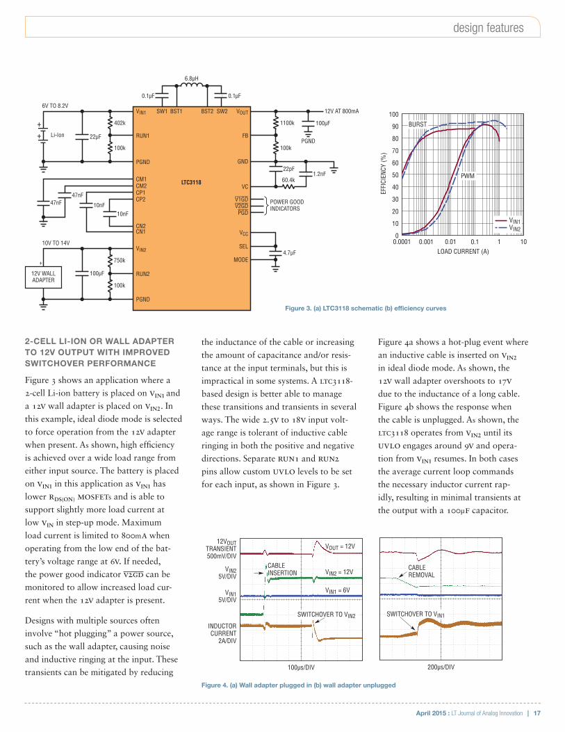
2-CELL LI-ION OR WALL ADAPTER TO 12V OUTPUT WITH IMPROVED SWITCHOVER PERFORMANCE
Figure 3 shows an application where a
2-cell Li-ion battery is placed on VIN1 and
a 12V wall adapter is placed on VIN2. In
this example, ideal diode mode is selected
to force operation from the 12V adapter
when present. As shown, high efficiency
is achieved over a wide load range from
either input source. The battery is placed
on VIN1 in this application as VIN1 has
lower RDS(ON) MOSFETs and is able to
support slightly more load current at
low VIN in step-up mode. Maximum
load current is limited to 800mA when
operating from the low end of the bat-
tery’s voltage range at 6V. If needed,
the power good indicator V2GD can be
monitored to allow increased load cur-
rent when the 12V adapter is present.
Designs with multiple sources often
involve “hot plugging” a power source,
such as the wall adapter, causing noise
and inductive ringing at the input. These
transients can be mitigated by reducing
the inductance of the cable or increasing
the amount of capacitance and/or resis-
tance at the input terminals, but this is
impractical in some systems. A LTC3118-
based design is better able to manage
these transitions and transients in several
ways. The wide 2.5V to 18V input volt-
age range is tolerant of inductive cable
ringing in both the positive and negative
directions. Separate RUN1 and RUN2
pins allow custom UVLO levels to be set
for each input, as shown in Figure 3.
Figure 4a shows a hot-plug event where
an inductive cable is inserted on VIN2
in ideal diode mode. As shown, the
12V wall adapter overshoots to 17V due to the inductance of a long cable.
Figure 4b shows the response when
the cable is unplugged. As shown, the
LTC3118 operates from VIN2 until its
UVLO engages around 9V and opera-
tion from VIN1 resumes. In both cases
the average current loop commands
the necessary inductor current rap-
idly, resulting in minimal transients at
the output with a 100µF capacitor.
LOAD CURRENT (A)0.0001
EFFI
CIEN
CY (%
)
40
60
10
20
00.001 0.01 0.1 1
100
30
50
10
70
80
90
VIN1VIN2
PWM
BURST402k
100k
1100k
12V AT 800mA
100k
60.4k
47nF47nF
6V TO 8.2V
10nF
22µF
100µF
PGND
POWER GOODINDICATORS
100µF
750k
10nF
22pF
10V TO 14V
Li-Ion
++
4.7µF
BST1 BST2VIN1 SW1 SW2
CM1
PGND
CM2
RUN1
CP1CP2
VOUT
VC
GND
V1GD
FB
V2GDPGD
CN2CN1 VCC
SEL
MODE
VIN2
PGND
RUN2
LTC3118
100k
1.2nF
+
12V WALLADAPTER
6.8µH
0.1µF0.1µF
Figure 3. (a) LTC3118 schematic (b) efficiency curves
12VOUTTRANSIENT500mV/DIV
INDUCTORCURRENT
2A/DIV
VIN25V/DIV
VIN15V/DIV
VOUT = 12V
VIN2 = 12V
VIN1 = 6V
SWITCHOVER TO VIN2
CABLE INSERTION
100µs/DIV
SWITCHOVER TO VIN1
CABLE REMOVAL
200µs/DIV
Figure 4. (a) Wall adapter plugged in (b) wall adapter unplugged

18 | April 2015 : LT Journal of Analog Innovation
operation. Figure 6a shows the transi-
tion from a 100mA load where the part
operates in Burst Mode, to a 600mA load
step where the LTC3118 enters PWM mode
quickly, minimizing the VOUT transient.
Note that USB 3.0 supports up to 1.5A for charging, but is restricted to 900mA during data transfer, the proposed USB 3.1 standard supports up to 2A.
Since the LTC3118 has a fixed inductor
current limit of 3A (minimum), the maxi-
mum amount of load current that can be
USB/SYSTEM POWER OR 3 Li-Ion CELLS IN PRIORITY MODE WITH BURST ENABLED TO IMPROVE BATTERY LIFE
A second LTC3118-based application is
shown in Figure 5. In this example, the
3-cell Li-ion battery stack is placed on
VIN2, where VIN1 is used for the USB input.
Since operation from the lower voltage
USB input should be favored when avail-
able, the LTC3118 is set to VIN1 Priority
mode. When operating from the USB, VIN1
and VOUT will be similar in voltage. At
the boundary between step-up and step-
down modes, the LTC3118’s internal PWM circuit seamlessly transitions, resulting in
minimal inductor and output voltage jitter.
Burst Mode operation provides improved
efficiency at light load from either source,
as shown in Figure 5b. While light load
efficiency is clearly important for the
battery input, the USB input may ben-
efit as well if powered from another
portable device. The LTC3118’s average
current mode control provides excellent
load step response, even in Burst Mode
supported in (or approaching) step-up
mode is reduced with VIN as shown in
Figure 6b for both 5V and 12V outputs.
This is an important consideration when
determining the input source voltages as
they relate to the required output voltage
and power budget for the load. If the
LTC3118’s VCC supply is back-fed from the
5V output as shown in Figure 5a, maxi-
mum load current at low input voltages
can be improved, as shown in Figure 6b.
3.3µH
0.1µF0.1µF
232k+
100k
402k
5V UP TO 1.5A,VIN > 4.5V
100k
40.2k
47nF47nF
4V TO 5.5V
10nF
22µF
100µF
PGND
POWER GOODINDICATORS
22µF
523k
10nF
22pF
SYSTEMPOWER
7.5V TO 12.6V
Li-Ion
+++
4.7µF BAT-54SCHOTTKY DIODE
BST1 BST2VIN1 SW1 SW2
CM1
PGND
CM2
RUN1
CP1CP2
VOUT
VC
GND
V1GD
FB
V2GDPGD
CN2CN1 VCC
SEL
MODE
VIN2
PGND
RUN2
LTC3118
100k
1.8nF
LOAD CURRENT (A)0.0001
EFFI
CIEN
CY (%
)
40
60
10
20
00.001 0.01 0.1 1
100
30
50
10
70
80
90
VIN1VIN2
PWM
BURST
Figure 5. (a) LTC3118 schematic (b) efficiency curves
VOUT200mV/DIV
IL2A/DIV
ILOAD1A/DIV
VC200mV/DIV
100µs/DIVVIN1 = VIN2 = 5V100mA to 1A LOAD STEP
VIN1 OR VIN2 VOLTAGE (V)2
MAX
IMUM
LOA
D CU
RREN
T (A
)
2.5
18
1.5
06 14 164 8 1210
3.5
2.0
3.0
1.0
0.5
12VOUTL = 6.8µH
5VOUTL = 3.3µH
DIODE FROM VOUT = 5V TO VCC
Figure 6. (a) Load step performance in Burst Mode operation. (b) Maximum load current for 5Vout and 12Vout

April 2015 : LT Journal of Analog Innovation | 19
design features
BACKUP SYSTEM
Figure 7 shows a backup power system
where the primary power source on VIN1
is supplied by a 12V system rail or lead
acid battery. A 10mF capacitor reservoir on
VIN2 is charged up to 18V from a separate
supply not shown. In the event the priority
VIN1 supply is interrupted, the V1GD indica-
tor transitions high to alert the system,
and the LTC3118 commences operation
from VIN2 to keep VOUT in regulation.
A scope photo of the backup event
is shown in Figure 7, where a 200mA load is supported for over a second to
allow a controlled shutdown. Available
energy at the input is given by:
( )= −
= −
=
E 12
C • V V
10mF • 18 2.22
1.6J
IN IN INITIAL2
FINAL2
2 2
In this case, a constant 200mA load
is drawn from the LTC3118 as the VIN capacitors are depleted in 1.35 seconds.
Output energy is 1.35 joules resulting in
an average conversion efficiency of 84%
including the supercapacitor losses.
===
E I • V • t200mA • 5 • 1.351.35J
OUT OUT OUT
VCC is back fed from VOUT, allowing VIN2
to operate down to 2.2V during the event.
The RUN2 pin is connected between VIN2
and VOUT in this case, requiring system
power on VIN1 to initially start-up VOUT and ensure clean shutdown behavior as
VIN2 decays during the backup event as
shown. The storage capacitance and volt-
age on VIN2 can be easily modified depend-
ing on the requirements of the system.
SUMMARY
The LTC3118 combines an intelligent
PowerPath controller with a single induc-
tor buck-boost converter, resulting in a
compact platform for multi-input designs.
The wide input/output voltage range and
ability to support 2A of load current in
step-down mode provides a robust solu-
tion for a wide variety of applications.
The LTC3118’s unique switch architec-
ture allows operation from the higher or
lower input voltage to a regulated output
voltage. The IC contains the necessary
control and indicator pins to give the
designer maximum system flexibility.
Average current mode control provides
rapid response for output load steps or
input line steps during switchover. With
Linear’s latest generation buck-boost core
and Burst Mode operation, both low noise
and high efficiency can be achieved. n
768k+
100k
402k
100k
40.2k
40.2k
47nF
47nF
10.5V TO 14.5V
10nF
22µF
47µF
5V
PGND
BAT-54SCHOTTKY DIODE
POWER GOODINDICATORS
VCC BACK FED FROM VOUTFOR LOW VIN OPERATION
22µF
2M
10nF
10mFCAPACITORBACKUP
22pF
LEAD ACID BATTERY OR 12VSYSTEM POWER
18V MAX, RUNSDOWN TO 2.2V
+
4.7µF
BST1 BST2
VIN1
SW1 SW2
CM1
PGND
CM2
RUN1
CP1CP2
VOUT
VC
GND
V1GD
FB
V2GDPGD
CN2CN1 VCC
SEL
MODE
VIN2
PGND
RUN2
LTC31181.8nF
3.3µH
0.1µF0.1µF
40.2k
CAN’T RUN FROM VIN2 UNTIL VOUT STARTS UP
Figure 7. Backup system holds up system for more than one second to allow for data storage
200ms/DIV
VIN210V/DIV
VIN110V/DIV
VOUT5V/DIV
INDUCTORCURRENT
1A/DIV

20 | April 2015 : LT Journal of Analog Innovation
SELECTED DEMO CIRCUITS
For a complete list of example simula-
tions utilizing Linear devices, please
visit www.linear.com/democircuits.
Linear Regulators
• LT3063: 1.8V Low noise regulator with
output discharge (2.3V to 1.8V at
200mA) www.linear.com/solutions/5246
Buck Regulators
• LT3667: 40V step-down regulator
with dual LDOs (6V–40V to 5V at 200mA, 2.5V/3.3V at 100mA) www.linear.com/solutions/5359
• LT8609: 5V, 2MHz, μPower step-down
regulator (5.5V–40V to 5V at 2A) www.linear.com/LT8609
• LT8640: 5V 2MHz μPower ultralow EMI step-down converter (5.7V–42V to 5V at
5A) www.linear.com/solutions/5635
• LTM4625: 5A buck µModule
regulator (4V–20V to 1.5V at 5A) www.linear.com/solutions/5613
• LTM4630: High efficiency single 36A step-down regulator (4.5V–15V to 1V at
36A) www.linear.com/solutions/5618
Buck-Boost Regulators
• LT3790: 240W high efficiency parallel
buck-boost regulator (8V–6V to 12V at
10A) www.linear.com/solutions/5464
• LTM8055: High efficiency buck-boost
regulator with accurate current limit &
output current monitor (5V–36V to 12V at 6A) www.linear.com/solutions/5690
• LTM8056: High efficiency buck-boost
regulator with accurate current limit &
output current monitor (7V–58V to 24V at 3A) www.linear.com/solutions/5694
Isolated Converter
• LTM8046: 5V isolated flyback
converter (3.2V–26V to 5V at 350mA) www.linear.com/solutions/5228
Constant Voltage, Constant Current Regulators
• LT3081/LT8612/LTC3632: 24V 3A constant
voltage, constant current bench
supply (10V–40V to 0-25V at 0A–3.1A) www.linear.com/solutions/5086
• LT8705: Bidirectional buck-boost
supercapacitor backup supply
(36V–80V to 15VCAP at 1A) www.linear.com/solutions/1751
SELECT MODELS
To search the LTspice library for a par-
ticular device model, choose Component
from the Edit menu or press F2.
Isolated Converter
• LTM8057: 3.1V–31V VIN isolated
µModule DC/DC converter
www.linear.com/LTM8057
Supercap Charger
• LTC3355: 20V 1A buck DC/DC with
integrated supercap charger and backup
regulator www.linear.com/LTC3355
Linear Regulators
• LT3086: 40V, 2.1A low dropout adjustable
linear regulator with monitoring
and cable drop compensation
www.linear.com/LT3086
What’s New with LTspice IV?Gabino Alonso
BLOG BY ENGINEERS, FOR ENGINEERS
Check out the LTspice® blog
(www.linear.com/solutions/LTspice)
for tech news, insider tips and interest-
ing points of view regarding LTspice.
New Article: “Loop Gain and its Effect on Analog Control Systems” by Simon Bramble www.linear.com/solutions/5587
This article brings together the concepts of
open loop gain, closed loop gain, gain and
phase margin, and minimum gain stability,
and shows how these parameters are inter-
related in a feedback system. It examines
loop gain in terms of a theoretical con-
trol system as well as practical electronic
circuits, including linear regulators.
LTspice® IV is a high performance SPICE simulator, schematic capture and waveform viewer designed to speed the process of power supply design. LTspice IV adds enhancements and models to SPICE, significantly reducing simulation time compared to typical SPICE simulators, allowing one to view waveforms for most switching regulators in minutes compared to hours for other SPICE simulators.
LTspice IV is available free from Linear Technology at www.linear.com/LTspice. Included in the download is a complete working version of LTspice IV, macro models for Linear Technology’s power products, over 200 op amp models, as well as models for resistors, transistors and MOSFETs.
What is LTspice IV?
—Follow @LTspice at www.twitter.com/LTspice —Like us at facebook.com/LTspice

April 2015 : LT Journal of Analog Innovation | 21
design ideas
• LT8613: 42V, 6A synchronous
step-down regulator with current
sense and 3µA quiescent current
www.linear.com/LT8613
• LTM4623: Ultrathin 20V VIN, 3A step-
down DC/DC µModule regulator
www.linear.com/LTM4623
Boost/SEPIC/Inverting Regulator
• LT8580: Boost/SEPIC/inverting DC/DC converter with 1A, 65V switch,
soft-start and synchronization
www.linear.com/LT8580 n
SPEED UP YOUR SIMULATIONS
LTspice is designed from the ground up to produce fast circuit simulations, but there is margin in some simulations to increase the speed. Note, there may be trade-offs in accuracy using the methods described here. For further details on any of these approaches, please refer to the LTspice Help File (F1). To measure the effects of your changes, review the simulation time in the LTspice error log (Ctrl + L).
Reduce Power Supply Start-Up TimeReduce the time required for switch mode power supply (SMPS) simulation by shortening the voltage ramp of the output by changing the value of the soft-start capacitor. Before doing so, make sure you have a good understanding of the power supply’s start-up performance. Then, reduce the soft-start capacitor value—using 0.001µF instead of the of the 0.1µF default—to quickly ramp to the desired output voltage.
Note that the soft-start capacitor should not be decreased to the point where the rising output allows the VC/Ith pin to ramp well beyond its nominal control point and slew further down to stop overshoot.
Delay the Application of the Load to a Power SupplyAnother effective technique to speed up simulation of an SMPS is to delay application of the load via a voltage controlled switch (SW). By using a switch that turns on the main load when the output voltage is near regulation (or at a known time), all the SMPS output energy goes into charging up the large output capacitors prior to the load being applied. A simpler approach can be achieved using a current load configured with a pulse function.
Set the Initial ConditionsSimilarly, it might be effective to use the .ic spice directive to set initial conditions for selected nodes. For example, specify the initial voltage on the output so that it is close to regulation when the simulation starts. Likewise, you can specify the voltage at the compensation node to eliminate the initial droop at start-up.
.ic V(out)=11 V(vc)=1
Reduce the Amount of Transient Analysis DataNormally, LTspice transient analysis starts at time = 0. You can edit the .trans simulation command’s “Time to start saving data” to delay saving until a later time of interest, thus decreasing your overall simulation time. Of course this assumes you do not need the initial data points, which are not saved.
Alternately, if you are only interested in a few node voltages and device currents, you can restrict the quantity of saved data by using the .save directive to save only those specific node voltages and device currents. In the directive, add the “dialogbox” option to display all available nodes and currents so you can choose to save additional data of interest.
.save V(out) I(L1) V(in) dialogbox
Skip the Initial Operating Point SolutionOccasionally you will notice that a simulation stays in “Damped Pseudo-Transient Analysis” for a long period of time (see the lower left corner of the window for simulation status information). This usually occurs when a DC solution is sought in order to find the operating point of the circuit. If it is acceptable in your
simulation, you can select Esc to skip finding the initial operating point and continue with the simulation. Likewise you can also “Skip initial operating point solution” by editing the simulation command.
If you prefer to save a difficult to solve DC operating point, you can use the .savebias command to save the preferred solution to a file in the initial simulation, and then in subsequent simulations, use the .loadbias command to quickly find the DC solution before proceeding with the rest of the simulation.
Use .savebias directive in initial simulation:.savebias filename.txt internal time=10m
Used .loadbias in subsequent simulations:.loadbias filename.txt
Convert to Fast Access Format When Viewing WaveformsTo maintain fast simulation speed, LTspice uses a compressed binary file format that allows additional simulation data to be quickly appended on the fly. However, once the simulation has completed, this format is non-optimal for waveform viewing. To speed up waveform plotting after the simulation is complete, convert the file to an alternate, “Fast Access,” format. Click in the waveform window and choose Files > Convert to Fast Access. This can also be implemented using the .option fastaccess directive:
.option fastaccess
It is important to note that in some simulations this conversion may take longer than the actual simulation.
Power User Tip
Happy simulations!
Buck Regulators
• LT3697: USB 5V, 2.5A output, 35V input
buck with cable drop compensation
www.linear.com/LT3697
• LT8610AC: 42V, 3.5A synchronous step-
down regulator with 2.5µA quiescent
current www.linear.com/LT8610AC

22 | April 2015 : LT Journal of Analog Innovation
There are a number of situations where a
synchronous boost LED driver is not avail-
able for a particular application. For some
of these cases, a synchronous buck LED driver IC can be used, but instead of oper-
ating as a step-down converter, it operates
as a step-up, or boost mode* LED driver.
For instance, take the LT3744 40V synchro-
nous buck LED driver, which is designed
to drive high current LEDs for projectors.
It features a versatile, floating VEE output
that allows it to be used in both high
current buck applications and positive-to-
negative (buck-boost) topologies where
the anode of the high current LED is con-
nected to ground to satisfy heat-sinking
requirements. It is the floating VEE feature
that allows us to effectively use this part,
originally designed for buck applications,
as a synchronous boost mode LED driver.
LT3744 BOOST MODE LED DRIVER
The LT3744 synchronous boost mode LED driver shown in Figure 1 regulates a 3A, 25V (75W) LED string from an automotive
input (9V–16V) at 98% efficiency. Even at
this power level, the maximum compo-
nent temperature rise is 45ºC with a 12V input, as shown in Figure 2. The IC enables
easy implementation of both 10:1 analog
and 100:1 PWM dimming at 120Hz with
ground-referred input signals, even though
neither the LED string nor the PWM dim-
ming MOSFET are connected to GND.
Although the 5mΩ sense resistor sets a 10A peak switch current in this application, the
solution can be altered to operate with a
6V input and a 15A peak switch current;
with an appropriately valued inductor
and a lowered undervoltage lockout.
The negative VEE rail on the LT3744
can reach −21V. The LT3744 simplifies
design by handling the level-shifting of
ground referenced input control signals.
Can’t Find the Right Synchronous Boost LED Driver? Use a Synchronous Buck Converter Instead: Boost Mode Topology Drives 25V, 3A LEDs from 12V Keith Szolusha
Synchronous buck converter drivers are commonly used when the current required for high power LEDs, such as 10A–40A projector LEDs, would overstress the components in a nonsynchronous converter. Synchronous rectification limits power losses and thermal rise due to high current in the converter switches. Synchronous rectification can offer the same benefits in high power step-up (boost) LED drivers—even with 1A to 3A LEDs. In contrast to a buck converter, the peak switch current of a boost can be much higher than the LED current, especially when output power is high and the input voltage is low.
VIN
TG
BG
PWM_OUT1PWM_OUT3PWM_OUT2
FB
VC1VC2VC3
VEE
VFNEG
ISPISN
BOOST
SW
VEE
INTVCC
VREF
CTRLT
SGND
LT3744
FAULT
M1, M2: INFINEON BSC026N04LSM3: INFINEON BSC010N04LSD1: PMEG4002EBD2: PMEG4010L1: WÜRTH 7443551470 4.7µH
EN/UVLO
CTRL1CTRL2CTRL3
PWM1PWM2PWM3SYNC
SS
2V0V
200k
VIN9V TO 16V
30.9k
EN/UVLO
RTVEE
L14.7µH
25V3A LED
5mΩ
VEE VEE
102k680pF
10nF
20k
100k
30.1k
10k
2.2nF
2V
VEE
20mΩ
D2
M3
43.2k
1M
M2
M1
4×10µF50V
2×10µF25V
VEE
VEE
VEE
D1
10µF
1µF25V
220nF
LED_ISN
LED_ISP
Figure 1. Boost mode 9V–16V input to 25V, 3A LED driver with 98% efficiency

April 2015 : LT Journal of Analog Innovation | 23
design ideas
A simple ground referenced PWM input
signal is level shifted to PWMOUT, so
no additional level shifting circuitry is
required to control the PWM MOSFET. Likewise, the LED current-setting sense
resistor can be tied directly to the nega-
tive VEE rail, all the way down to −21V.
LEVEL-SHIFTED GND AND VEE
The level-shifting, positive-to-negative
conversion, feature of the LT3744
LED driver is designed to support high
current grounded-anode LED drivers.
Nevertheless, the same feature can be
used for boost mode applications where
the LED string is connected between VIN and a negative VEE potential. Because the
LED sense resistor and PWM dimming
MOSFET are both located at the bot-
tom of the LED string, the level-shifted
PWMOUT signal from the ground-referred
PWM input yields a topology that looks
no more complicated than a traditional
Figure 2. Boost mode LED thermal scan shows cool operation.
VIN = 12V VLED = 23.45V ILED = 3A NO FORCED AIR
S1
S2
COUTCIN
L1VIN VOUT
S1S2
COUTCIN
VEE (NEGATIVE) = LED–
L1VIN
VIN = LED+
CONTINUOUS MODE
VOLTAGE CURRENT
IIN
0
VOUT
VIN
VIN
VIN
VOUT
0
00
0
0
0
VIN – VOUT
VOUT
IOUT
0IOUT
0IOUT
0IOUT
0
COUT
L1
D1
S1
CONTINUOUS MODE
VOLTAGE CURRENT
IIN
0
VOUT
VIN
VIN
VIN
VOUT
0
00
0
0
0
VIN – VOUT
VOUT
IOUT
0IOUT
0IOUT
0IOUT
0
COUT
L1
D1
S1
VOUT = VLED
–
+Figure 3. Boost mode current ripple, duty cycle and voltage stress are the same as those of traditional boost regulators.
Synchronous rectification is a feature commonly called on to limit power losses in high power LED drivers. As shown, a synchronous buck LED driver can be used as a boost mode converter, capitalizing on the wide availability of this feature in high performance buck regulator ICs.

24 | April 2015 : LT Journal of Analog Innovation
boost PWM dimming setup. The input side
looks like a straightforward LED driver,
with CTRL analog dimming, SYNC input
and enable inputs all referred to signal
GND, no matter where negative VEE lies.
The LT3744’s VEE can go all the way down
to −21V. Open LED overvoltage protec-
tion is set at about 26.5V for the 25V VLED application. With some open LED overshoot in mind, this limits the VIN minimum to about 6V for a 25V VLED boost mode application before nega-
tive VEE goes beyond the −21V limit. To
operate at the minimum 6V input, the
solution in Figure 1 requires a lower
undervoltage lockout and a sense resis-
tor and inductor that can accommodate
15A peak switch current limit. With lower
VLED strings (at any current level), the
minimum input voltage can be dropped
to 4V VIN with some simple adjustments.
MORE ABOUT BOOST MODE
A boost mode converter has many of
the same properties of traditional boost
regulators. As shown in Figure 3, with
the exception of the unusual topological
hookup and the main control of high side
switch S1 instead of a low side switch,
this boost mode converter features the
same duty cycle, ripple current and volt-
age stress that a tradition boost converter
would. If synchronous rectification is not
required, a nonsynchronous buck regula-
tor can be used as a boost mode driver,
with S2 replaced by a typical catch diode
D1, as in a traditional boost regulator.
The gain-phase Bode plot in Figure 4
shows that even the control loop of boost
mode converter acts like a traditional
boost regulator. With a 10kHz crossover
frequency, 60° of phase margin, and
−15dB of gain margin, the LED driver
shown in Figure 1 is stable and reliable.
CONCLUSION
Synchronous rectification is a feature com-
monly called on to limit power losses in
high power LED drivers. As shown here,
a synchronous buck LED driver can be
used as boost mode converter, capitalizing
on the wide availability of this feature
in high performance buck regulator ICs.
Specifically, the LT3744 synchronous buck
LED driver can be used as a high effi-
ciency 9V–16V input, 25V LED 3A boost
mode LED driver, yielding 98% efficiency
for a 75W converter. The unique ability
of this IC to level shift control signals as
needed from SGND to –VEE makes it pos-
sible to produce a floating boost mode
topology with no more components
than needed in a traditional boost. n
Notes:
* Boost mode is a patent pending technology.
FREQUENCY (kHz)1 10 100
–60
–50
–40
–30
–20
–10
0
10
20
30
40
50
60
–180
–150
–120
–90
–60
–30
0
30
60
90
120
150
180
GAIN
(dB)
PHASE (DEGREES)
Figure 4. Boost mode control loop gain and phase shows typical bandwidth.
The LT3744 synchronous buck LED driver can be used as a high efficiency 9V–16V input, 25V LED 3A boost mode LED driver, yielding 98% efficiency for a 75W converter. The unique ability of this IC to level shift control signals as needed from SGND to –VEE makes it possible to produce a floating boost mode topology with no more components than needed in a traditional boost.

April 2015 : LT Journal of Analog Innovation | 25
design ideas
How to Design an Isolated, High Frequency, Push-Pull DC/DC Converter Dawson Huang
The LT3999 monolithic DC/DC push-pull
driver avoids these issues with two impor-
tant features: duty cycle control and high
frequency operation:
•Duty cycle control allows compensation
for wide VIN variation—something stan-
dard fixed duty cycle transformer driv-
ers cannot do—greatly reducing LDO loss when facing a wide input range.
•High switching frequency, up to
1MHz, leads to smaller transform-
ers and lower output ripple.
The LT3999 combines these two
features with high 36V input voltage
and 1A input current capabilities,
making it a high power and flexible
low noise push-pull converter IC.
This article presents two step-by-
step design procedures: One for a
push-pull DC/DC converter with a
wide input range, the other for a
compact high frequency transformer
driver with fixed input voltage.
PUSH-PULL DC/DC CONVERTER DESIGN FOR WIDE RANGING INPUT
The flowchart in Figure 1b shows
how a push-pull converter can be
designed in eight simple steps. These
steps produce the LT3999 10V–15V input, ±12V output, 200mA 1MHz push-
pull converter shown in Figure 1a.
RT UVLO & OVLO/DC
RDC
RECTIFIER
INDUCTOR
LDO
SNUBBER
APPLICATION SPECIFICATIONS fSW, VIN(MIN), VIN(MAX), VOUT1, IOUT1, IOUT2
N = NP:NS
8
7
6
5
4
3
21
VIN
SYNC
UVLO
OVLO/DC
LT3999
L2
L1D1T1
D2
D3
D4
SWA • •
• •
VIN(MIN) TO VIN(MAX)
SWB
GND
R1
R2R3
R4 R4
RBIASRTRDC CSS
CIN
RD
C1C3 COUT1
VOUT
C2
RDC
RT
ILIM/SS
RBIAS
U1POSITIVE
LDO
U2NEGATIVE
LDO COUT2
–VOUT
8
7654
3
2
1
Figure 1. (a) LT3999 push-pull DC/DC converter with wide input range and duty cycle control (b) Easy 8-step push-pull converter design
(b)(a)
A simple push-pull DC/DC converter with a fixed 50% duty cycle is often used as a low noise transformer driver in communication systems, medical instruments and distributed power supplies. This simple scheme provides no voltage regulation—requiring a low dropout (LDO) post regulator—a combination that presents potentially serious problems. First, any significant variation in the driver’s input voltage, along with the fixed 50% duty cycle, can increase the differential voltage across the LDO, resulting in significant power losses and high temperature rise in the LDO. Second, low switching frequency requires relatively bulky transformers, sometimes occupying 30% to 50% of the converter space.

26 | April 2015 : LT Journal of Analog Innovation
Step 1: Set the Switching Frequency (RT)
First, set the switching frequency
with RT; the value chosen from
Table 1 in the LT3999 data sheet.
RT = 12.1k sets fSW = 1MHz.
Step 2: Set the Input Voltage Range (UVLO, OVLO/DC)
The UVLO (undervoltage lockout)
and OVLO/DC (overvoltage lockout/
duty cycle) pins are used to set input
voltage range. Either a 2- or 3-resistor
method can be used. For the 2-resistor
method shown in Figure 2a, RB is calculated using equations 1 and 2 for
UVLO and OVLO/DC, respectively. For
low loss, we can assume RA = 1MΩ.
For UVLO: RB UVLO( ) = RA
VIN MIN( )1.25
1
(1)
For OVLO:
RB OVLO( ) = RAVIN MAX( )
1.251
(2)
For the 3-resistor method shown
in Figure 2b, RA1 and RB are
calculated by equations 3 and 4 for
UVLO and OVLO/DC, respectively.
RA2 can be chosen around 1MΩ.
RA1 = RA2
1VIN MIN( )VIN MAX( )
VIN MIN( )1.25
1
(3)
RB = RA2
VIN MIN( )VIN MAX( )
VIN MIN( )1.25
1
(4)
For the 2-resistor method used in
Figure 1a:
VIN(MIN) = 10V, RA = 1M, RB = 143k.
VIN(MAX) = 15.5V, RA = 1M, RB = 86.6k.
Step 3: Set the Maximum Duty Cycle (RDC(MAX))
The maximum duty cycle (DCMAX) is determined by the switching period
(TS = 1/fSW) and non-overlap time (TD(MIN))
between the two power switches, as
shown in equation 5. For the 2-resistor
method, RDC is calculated by equation
6. For the 3-resistor method, substi-
tute RA = RA1 + RA2 in equation 6.
=−
DC T 2T
2TMAXS D(MIN)
S (5)
= +
R
V • RR R
•R •DC • 4
1.25
DC
IN(MIN)B
A BT MAX
(6)
In the Figure 1(a) example, TS = 1µs,
TD(MIN) = 70ns (typical value in the
data sheet), VIN(MIN) = 10V, RA = 1M,
RB = 143k. Calculations 5 and 6 give
DCMAX = 0.43, and RDC = 13.3k.
Step 4: Select the Transformer (T1)
The transformer turns ratio is
represented in equation 7.
( )
=
=+ + + +
−
N NN
V V V V 2V2 V V • 2DC
s
p
OUT1 OUT2 LDO1 LDO2 F
IN(MIN) SW max
(7)
VSW is the switch saturation voltage
for internal switches. VF is the forward
voltage of the rectifier diodes. VLDO1 and
VLDO2 are the dropout voltages of the
positive and negative LDOs. VSW = 0.4V, VF = 0.7V, VLDO1 = VLDO2 = 0.8V are good
rules of thumb. If a commercial trans-
former with an exact calculated turns
ratio cannot be found, select one that
is close and calculate DCMAX in equa-
tion 7 accordingly. Then, recalculate RDC in equation 6 based on new DCMAX.
In the Figure 1(a) example, VOUT1 =
−VOUT2 = 12V and VIN(MIN) = 10V, so choose
Wurth 750314781(N = 2) for DCMAX = 0.43.
Step 5: Design the Rectifier (D1, D2, D3 and D4)
The peak voltage across the rectifier bridge
is composed of the transformer secondary
side voltage (VSEC) plus any ringing voltage
spikes. VSEC is calculated using equation
8. The ringing voltage spike, however, is
difficult to predict, as it depends on the
loop resistance, the leakage inductance of
the transformer, and the junction capaci-
tance of the rectifiers. As general rule, the
rectifier voltage rating (VREC) should be at
VIN
UVLO
RA2
RA1
RA
RB
RB
OVLO/DC
VIN
UVLOOROVLO/DC
Figure 2. Setting the precision UVLO and OVLO/DC via resistor divider using either (a) a 2-resistor method or (b) a 3-resistor method.
(b)(a)
The LT3999 is a monolithic DC/DC transformer driver, which features duty cycle control, high frequency and high power. It allows a wide input voltage range and low loss at the LDO, while using small passive components due to the high frequency operation. It also features input voltage up to 36V and input current up to 1A.

April 2015 : LT Journal of Analog Innovation | 27
design ideas
least 1.5 times the transformer turns ratio
multiplied by the maximum input voltage.
Because the two secondary windings are
connected across the rectifier bridge, a
factor of two is required, producing the
formula for the rectifier voltage rating:
≥V 1.5 • 2N • VREC IN(MAX) (8)
The current rating of the rectifier (IREC) should be greater than the load current.
When VIN(MAX) = 15.5V, N = 2, VREC ≥ 93V, IREC ≥ 200mA: a Central CMSH1-200HE (200V, 1A) satisfies these requirements.
Step 6: Select the Inductors (L1, L2)
The minimum inductor value (LMIN) is set by the peak current limit of internal
switcher (ILIM) as shown by equation 9.
LMIN
=2N • VIN(MAX) • 1 2DCMIN( ) •DCMIN
TS2
2 ILIM2N
IOUT1
(9)
Higher inductance produces better regula-
tion and lower voltage ripple, but requires
a correspondingly greater volume part.
The optimum inductor value is deter-
mined by taking into account both output
noise and solution volume requirements.
When VIN(MAX) = 15.5V, DCMIN = 0.28, TS = 1µs, N = 2, ILIM = 1A, IOUT1 = IOUT2 = 200mA, LMIN = 38.3µH: A Coilcraft XFL3012-393MEC (39.3µH)
satisfies these requirements without
adding unnecessary size.
Step 7: Select the Low Dropout Linear Regulator (U2, U3)
The maximum voltage of LDO occurs
at maximum input voltage under no
load, when VSEC equals VIN(MAX) • N.
The current rating of the LDO should
be greater than the load current.
When VIN(MAX) = 15.5V, N = 2, the voltage
rating for the LDOs should be 31V and
−31V, satisfied by the LT3065 (45V, 500mA) and LT3090 (−36V, 400mA), respectively.
Step 8: Add a Snubber (CS and RS)
The recommended approach for design-
ing an RC snubber (CS and RS in Figure 1)
is to measure the period of the ringing at
the LT3999’s SWA and SWB pins when its
switchers turn off without the snubber,
and then add capacitance—starting with
something in the range of 100pF—until
the ringing period lengthens by 1.5x to 2x.
The change in period determines the value
of the parasitic capacitance (CPAR), from
which the parasitic inductance (LPAR) can
be determined from the initial period.
Similarly, initial values can be estimated
using data sheet values for switch capaci-
tance and transformer leakage inductance.
Once the value of the drain node capaci-
tance and inductance are known, a
series resistor can be added to the snub-
ber capacitance to dissipate power
and critically dampen the ringing. The
equation for deriving the optimal series
resistance using the observed periods
(tPERIOD, and tPERIOD(SNUBBED)) and snub-
ber capacitance (CS) is below. Refer to
the LT3748 data sheet for more details.
=
−( )
CC
t
t1
PARS
PERIOD SNUBBED
PERIOD
2
(10)
( )=π
Lt
C • 4PAR
PERIOD2
PAR2
(11)
=R LCSNUBBER
PAR
PAR (12)
RESULTS
The measured results in Figures 3, 4
and 5 show that duty cycle control in
the push-pull converter of Figure 1
maintains a low VIN − VOUT differential
across the LDOs, resulting in minimized
power loss and temperature rise. Figure 3
shows that at 200mA per LDO, VDIFF , remains under 2.5V over the entire input
voltage range of 10V–15V. Figure 4
shows power loss remains low across
the load current range. Figure 5 and
Figure 6 show the thermal results.
For comparison, Figure 7 shows the
efficiency comparison of the design with
duty cycle control disabled and duty
POW
ER L
OSS
(W)
V DIF
F (V
)
VIN (V)1610
8
0
4
011 12 13 14 15
4
3
2
1
6
5
7
2
1.5
1
0.5
3
2.5
3.5
POWER LOSS
IOUT1 = IOUT2 = 200mA
VDIFF
Figure 3. LDO (U2) VIN − VOUT differential and power loss vs input voltage
POW
ER L
OSS
(W)
V DIF
F (V
)
IOUT1 = IOUT2 (mA)2000
8
0
4
025 50 75 100 125 150 175
4
3
2
1
6
5
7
2
1.5
1
0.5
3
2.5
3.5
POWER LOSS
VDIFF
VIN = 10V
Figure 4. LDO (U2) VIN − VOUT differential and power loss vs load

28 | April 2015 : LT Journal of Analog Innovation
cycle control enabled. The efficiency
drops dramatically when input voltage
increases. Figure 8 shows the differen-
tial voltage across the positive LDO with
duty cycle control disabled and duty
cycle control enabled. Figures 9 and 10
show the thermal results. It is evident
that the duty cycle control reduces the
differential voltage and improves the
efficiency and thermal performance
COMPACT TRANSFORMER DRIVER FOR A FIXED INPUT VOLTAGE
Normally, the output voltage of the
basic unregulated transformer driver
converter changes significantly with
changes in load current. To produce a
regulated voltage, an LDO on the output
is strongly recommended. Figure 6a
shows the schematic of low part count
transformer driver using the LT3999.
Figure 6b shows the design flowchart.
The four simple steps in the flowchart
can be used to design a 1MHz, low parts
count, 5V input, 5V output 400mA out-
put transformer driver as an example.
Step 1: Set the Switching Frequency (RT)
The switching frequency of the LT3999 is
set by a single RT resistor selected based
on the table in the LT3999 data sheet
(frequency range is from 50kHz to 1MHz).
In the design example, for high
frequency fSW = 1MHz, RT = 12.1k.
Step 2: Select the Transformer (T1)
The transformer turns ratio is
determined by:
= =+ +
−N N
NV V V
V VS
P
OUT LDO(OPTIONAL) F
IN SW (13)
where VSW is the switch saturation volt-
age for internal switchers, and VF is the
forward voltage of a rectifier diode.
VLDO is the drop from the unregulated
transformer driver output to the post
regulated low noise output. VLDO is the
drop at highest current, so it should be
minimized. 0.8V provides enough drop to
avoid dropout without the LDO getting
hot. A good rule of thumb assumption
is VSW = 0.4V, VF = 0.7V, VLDO = 0.8V.
The current rating of the transformer
should be 20%~50% larger than the
output current to leave some room.
The sum of the peak magnetizing current
(IM(PEAK)) and the full load current
reflected to the primary side (N • IOUT) should less than the peak current limit
of the internal switcher (ILIM). Based on
this, minimal LM (LM(MIN)) is required.
EFFI
CIEN
CY (%
)
VIN (V)1610
70
2011 12 13 14 15
60
50
40
30
DUTY CYCLE CONTROLENABLED
DUTY CYCLE CONTROLDISABLED
V DIF
F (V
)
VIN (V)1610
8
011 12 13 14 15
4
3
2
1
6
5
7
DUTY CYCLE CONTROLENABLED
DUTY CYCLE CONTROLDISABLED
Figure 7. Efficiency comparison of the design with duty cycle control disabled and duty cycle control enabled, IOUT1 = IOUT2 = 200mA
Figure 8. LDO (U2) VIN − VOUT differential vs VIN at full load with duty cycle control disabled and with duty cycle control enabled, IOUT1 = IOUT2 = 200mA
Figure 5. Thermal image of the design in Figure 1 in action, VIN = 10V
VIN = 10V VOUT1 = 12V, VOUT2 = −12V IOUT1 = IOUT2 = 200mA NO FORCED AIR
U1
U3
U2T1
Figure 6. Thermal image, VIN = 15V
VIN = 15V VOUT1 = 12V, VOUT2 = −12V IOUT1 = IOUT2 = 200mA NO FORCED AIR
U1
U3
U2T1

April 2015 : LT Journal of Analog Innovation | 29
design ideas
+
= −
+
<
( )I N • I
V VL
• T4
N • I
I
M PEAK OUT
IN SW
M
SOUT
LIM
(14)
> −−
= ( )L V VI N • I
• T4
LMIN SW
LIM OUT
SM MIN
(15)
For VOUT = VIN = 5V, the Coilcraft
PA6383-AL (N = 1.5) is a good fit.
Step 3: Rectifier (D1, D2)
Choose the rectifier diodes based on
voltage and current. The voltage across
the diodes is more than twice that of the
transformer secondary voltage because
of its center tap structure. The voltage
rating of the rectifier should be larger
than 2N • VIN = 15V, maybe by 20%.
The CMSH1-20M (20V, 1A) satisfies these requirements.
Step 4: Low Dropout Linear Regulator (U2, Optional)
The maximum input voltage of
the optional post-regulating LDO (VLDO_IN(MAX)) occurs at no load,
where it equals VIN • N = 7.5V. The
current rating of the LDO should be
larger than the load current (>400mA in the case of the design example).
A good LDO for the 5V, 400mA output is the LT1763 (20V, 500mA).
CONCLUSION
The LT3999 is a monolithic DC/DC trans-
former driver, which features duty cycle
control, high frequency and high power. It
allows a wide input voltage range and low
loss at the LDO, while using small pas-
sive components due to its high frequency
operation. It also features input voltage
up to 36V and input current up to 1A. n
Figure 9. Thermal image of the design with duty cycle control disabled in circuit of Figure 1, VIN = 10V
VIN = 10V VOUT1 = 12V, VOUT2 = −12V IOUT1 = IOUT2 = 200mA NO FORCED AIR
U1
U3
U2T1
Figure 10. Thermal image of the design with duty cycle control disabled in circuit of Figure 1, VIN = 15V
VIN = 15V VOUT1 = 12V, VOUT2 = −12V IOUT1 = IOUT2 = 200mA NO FORCED AIR
U1
U3
U2T1
VIN
UVLO
SYNC
OVLO/DC
RDCLT3999
SWA
COUT
T1 D1
D2
VOUT• •
• •
VIN
SWB
GNDRBIASRT
CIN
RT
ILIM/SS
RBIAS
COUT1LDO
OPTIONAL
IN OUT
IN
4
32
1
RT
N = NP:NS
RECTIFIER
LDO
APPLICATION SPECIFICATIONS fSW, VIN, VOUT, IOUT
4
3
2
1
Figure 11. (a) Low parts count, fixed input voltage transformer driver. (b) Design flowchart for the transformer driver
(a) (b)

30 | April 2015 : LT Journal of Analog Innovation
New Product Briefs
500mA, 1.5MHz, 65V BOOST DC/DC CONVERTER
The LT8570 and LT8570-1 are current
mode, fixed frequency step-up DC/DC converters. The LT8570 uses an internal
500mA, 65V switch, whereas the LT8570-1
uses a 250mA, 65V switch. Both devices
operate from an input voltage range of
2.55V to 40V, making them suitable for
applications with input sources ranging
from a single-cell Li-ion to automotive
inputs. Both the LT8570 and LT8570-1 can
be configured as a boost, SEPIC or invert-
ing converter. The LT8570-1’s smaller
switch enables the use of a smaller induc-
tor in lower current applications. Both
parts offer a programmable switching
frequency between 200kHz and 1.5MHz,
enabling designers to minimize external
component sizes. The combination of a
3mm × 3mm DFN package (or MSOP-8E) and tiny externals ensures a very compact
footprint while minimizing solution cost.
The LT8570 and LT8570-1 use internal
high efficiency switches, which deliver
efficiencies up to 86%. Undervoltage
lockout (UVLO) is user adjustable for
optimal system performance. A single
feedback resistor sets the output voltage,
minimizing external components. Other
features include external synchroniza-
tion capability, internal soft-start, thermal
shutdown protection and the ability to
work in inverting and SEPIC applications.
The LT8570/-1 is available in both a
3mm × 3mm DFN-8 and a thermally
enhanced MSOP-8 package.
140V, 400mA STEP-DOWN CONVERTER WITH ONLY 12µA QUIESCENT CURRENT
The LTC7138 is a 140V input-capable high
efficiency buck converter that delivers up
to 400mA of continuous output current.
It operates from an input voltage range
of 4V to 140V, making it ideal for a wide
range of telecom, industrial, avionic and
automotive applications. The LTC7138
utilizes a programmable hysteretic mode
design to optimize efficiency over a broad
range of output currents. It utilizes an
internal 1.8Ω power MOSFET for robust,
high efficiency operation. A user-pro-
grammable output current limit can set
output current from 100mA to 400mA as required by the particular applica-
tion. The LTC7138 can be programmed
with fixed output voltages of 1.8V, 3.3V or 5V, or a resistor divider can be used
to program outputs from 0.8V to VIN. The LTC7138’s thermally enhanced MSOP offers additional pin spacing required
for high voltage inputs. The combination
of its MSOP and only four tiny exter-
nals provides a highly compact solution
footprint for a wide array of applications.
The LTC7138 draws only 12µA at no load
while maintaining output voltage regula-
tion, making it ideal for always-on battery-
powered applications. Due to the inherent
stability of the converter, no external
compensation is required, thereby simpli-
fying design and minimizing the solution
footprint. Additional features include a
precise 0.8V +1% feedback voltage refer-
ence, 100% duty cycle dropout operation
and, internal or external soft-start, and
a feedback comparator output which
enables multiple LTC7138s to be connected
in parallel for higher current applications.
POWER FACTOR CORRECTION BOOST CONTROLLER
The LT8312 is a power factor correction
(PFC) boost controller that can achieve
a power factor of greater than 0.99 by
actively modulating the input current,
allowing compliance with most harmonic
current emission requirements. This device
operates with current mode control and
critical conduction mode—a variable
frequency switching scheme that returns
the current to zero in the inductor with
every cycle. This switching behavior is
similar to zero voltage switching, which
minimizes electromagnetic interference
and energy lost in the power switch,
improving efficiency as much as 5%.
The LT8312 is suitable for universal AC (90 265VAC) input and higher ranges,
depending on the choice of external
components. The LT8312 uses hysteretic
start-up, eliminating the need for a bias
power supply. After start-up, the device
is powered by a bootstrap winding off
of the inductor. With a strong 1.9A gate
driver, the LT8312 drives most high voltage
MOSFETs. The low 102mV current sense
threshold facilitates the use of small value
shunt resistors, which increase efficiency.
The LT8312 is available in a 16- lead
MSOP package.

April 2015 : LT Journal of Analog Innovation | 31
product briefs
HIGH EFFICIENCY SWITCHING SURGE STOPPER PROTECTS AGAINST 200V & HIGHER TRANSIENTS
The LTC7860 is a high efficiency switch-
ing surge stopper with overvoltage and
overcurrent protection for high availability
systems. During normal operation the
LTC7860 turns on an external P-channel
MOSFET continuously to pass the input
voltage through to the output with mini-
mum conduction loss. During an input
overvoltage condition, the LTC7860 con-
trols the external MOSFET to operate as a
high efficiency switching DC/DC regulator
to protect critical downstream components
by limiting the output voltage and current.
The LTC7860 builds on our popular linear
surge stoppers such as the LTC4363 by
offering high efficiency switching protec-
tion to extend output current capability
and reduce power loss during transients
and faults. Supply voltages surge when
the load current changes abruptly in long
inductive power busses. The situation is
aggravated in automotive applications by
the energy stored in the alternator induc-
tance, causing an elevated and extended
voltage surge during a load dump. The
power handling capability of a surge
stopper is limited by the power lost in the
protection device. In a linear surge stopper,
the power capability is determined by the
size of the pass MOSFET, while in a switch-
ing surge stopper the power capability
is determined by conversion efficiency.
Due to its lower power loss, a switch-
ing surge stopper can operate through
longer input voltage surges at higher
output current than a linear solution.
The LTC7860 has an input voltage operat-
ing range of 3.5V to 60V, which can be
extended with external circuitry up to
200V and higher. An external fault timer
capacitor configures the limited time
spent in overvoltage mode and keeps
the switching surge stopper below a
safe peak operating temperature when
power loss is at its highest levels. The
fault timer reduces system cost and
size by optimizing component selection
for normal mode rather than overvolt-
age transient and fault conditions.
In MIL-STD-1275 applications, the LTC7860
protects devices operating from a 28V vehicle power bus which can reach as high
as 100V for up to 500ms. The LTC7860 is
ideal for industrial, avionics and auto-
motive power applications including
ISO7637, as well as positive high voltage
distributed power Hot Swap™ systems.
The LTC7860 is available in a thermally
enhanced 12-lead MSOP package.
ULTRALOW VOLTAGE STEP-UP ENERGY HARVESTER & POWER MANAGER IC EXTENDS USEFUL LIFE OF PRIMARY BATTERIES IN WSNs
The LTC3107, a highly integrated DC/DC converter designed to extend the life of
a primary battery in low power wireless
system networks (WSNs). The LTC3107
combines energy harvesting and power
management capability with a primary
battery cell to extend the battery’s usable
lifetime. The LTC3107 harvests energy
from thermoelectric generators (TEGs) and
thermopiles when these sources are avail-
able, storing excess power in a storage
capacitor and seamlessly transitioning to
the primary cell to power a wireless sensor
node when harvested power is unavailable.
The LTC3107’s internal boost converter,
combined with a small step-up trans-
former, harvests energy from input volt-
ages as low as 20mV, commonly found
from sources such as TEGs and thermo-
piles, and delivers an output which tracks
the battery voltage. An additional 2.2V LDO output provides power to an exter-
nal microprocessor. If harvested energy
is not available, the system is powered
directly from the battery, requiring only
6µA. The combination of a small step-up
transformer, 3mm × 3mm package and
minimal external components ensures
a highly compact solution footprint.
The LTC3107 is designed to use the pri-
mary battery to start up the IC and power
VOUT and the LDO with or without any
available power from the energy harvest-
ing source. When the energy harvesting
source is available, the LT3107 seamlessly
transitions to run solely from the energy
harvesting source with only 80nA of
quiescent current drawn from the primary
battery. If the energy harvesting source
goes away or if the load exceeds the
energy harvested, the LT3017 transitions
to the primary battery to supply the VOUT and VLDO loads. The BATT_OFF indicator
can be used to track the battery usage.
The LTC3107EDD is offered in a
3mm × 3mm 10-lead DFN package. n
The LT8312 is a power factor correction (PFC) boost controller that can achieve a power factor of greater than 0.99 by actively modulating the input current, allowing compliance with most harmonic current emission requirements. This device operates with current mode control and critical conduction mode—a variable frequency switching scheme that returns the current to zero in the inductor with every cycle.

highlights from circuits.linear.com
Linear Technology Corporation 1630 McCarthy Boulevard, Milpitas, CA 95035 (408) 432-1900 www.linear.com Cert no. SW-COC-001530
L, LT, LTC, LTM, Linear Technology, the Linear logo, Burst Mode, Dust Networks, LTspice, Silent Switcher and µModule are registered trademarks, and Hot Swap and PowerPath are trademarks of Linear Technology Corporation. All other trademarks are the property of their respective owners. © 2015 Linear Technology Corporation/Printed in U.S.A./68.5K
LTC2956 WAKE-UP TIMER WITH PUSHBUTTON CONTROLThe LTC®2956 is a micropower, wide input voltage range, configurable wake-up timer with pushbutton control. It periodically wakes up and turns on a connected system to perform tasks such as monitoring temperature or capturing images. After completing the task, the LTC2956 turns the system off to conserve power.www.linear.com/solutions/5702
TWO LTM8056s PARALLELED AND SYNCHRONIZED, VIN 7V–58V, VOUT 18V AT 8AThe LTM®8056 is a 58V input, buck-boost μModule® (micromodule) regulator. Included in the package are the switching controller, power switches, inductor and support components. Only a resistor to set the switching frequency, a resistor divider to set the output voltage, and input and output capacitors are needed to complete the design. Other features such as input and output average current regulation can be implemented with just a few components. The LTM8056 operates over an input voltage range of 5V to 58V, and can regulate output voltages between 1.2V and 48V. The SYNC input and CLKOUT output allow easy synchronization.www.linear.com/solutions/5693
PBOUT
SLEEP
OFFALERT
ONALERTTURNING OFF
TURNED ON
PBGND
ONMAX
VBAT
ENVIN
RANGE
VOUTVIN
LT3060
SHDN
LTC2956-1
LONG
VMAIN
1.5nF
µP
100k
10k
1µF
10k
10k
280k 9.76k
PERIOD
100k
tLONG = 1s, tONMAX = 20ms, tPERIOD = 250ms
+
VIN
SVIN
IIN
GNDLLMODE
LTM8056
IOUT
0.015ΩVOUT
IINMONIOUTMON
FB
RUNCTLSSSYNCCOMPRTCLKOUT
VOUT18V
2.2µF100V×4 1µF
VIN7V TO 58V
30.9k680kHz
VIN
SVIN
IIN
GND
LTM8056
IOUT
0.015ΩVOUT
CTLCLKOUT
IINMONIOUTMON
FB
RUNCOMPSSSYNC
RT
6.98k
LT6015
100k
6.34k
2.2µF100V×4
1µF
30.9k680kHz
LLMODE
51Ω
100k22µF25V
47µF25V
22µF25V
47µF25V
+
+