application note: methods and problems in evaluating high
TRANSCRIPT
1
Methods and Problems in Evaluating High-Speed Jitter Tolerance
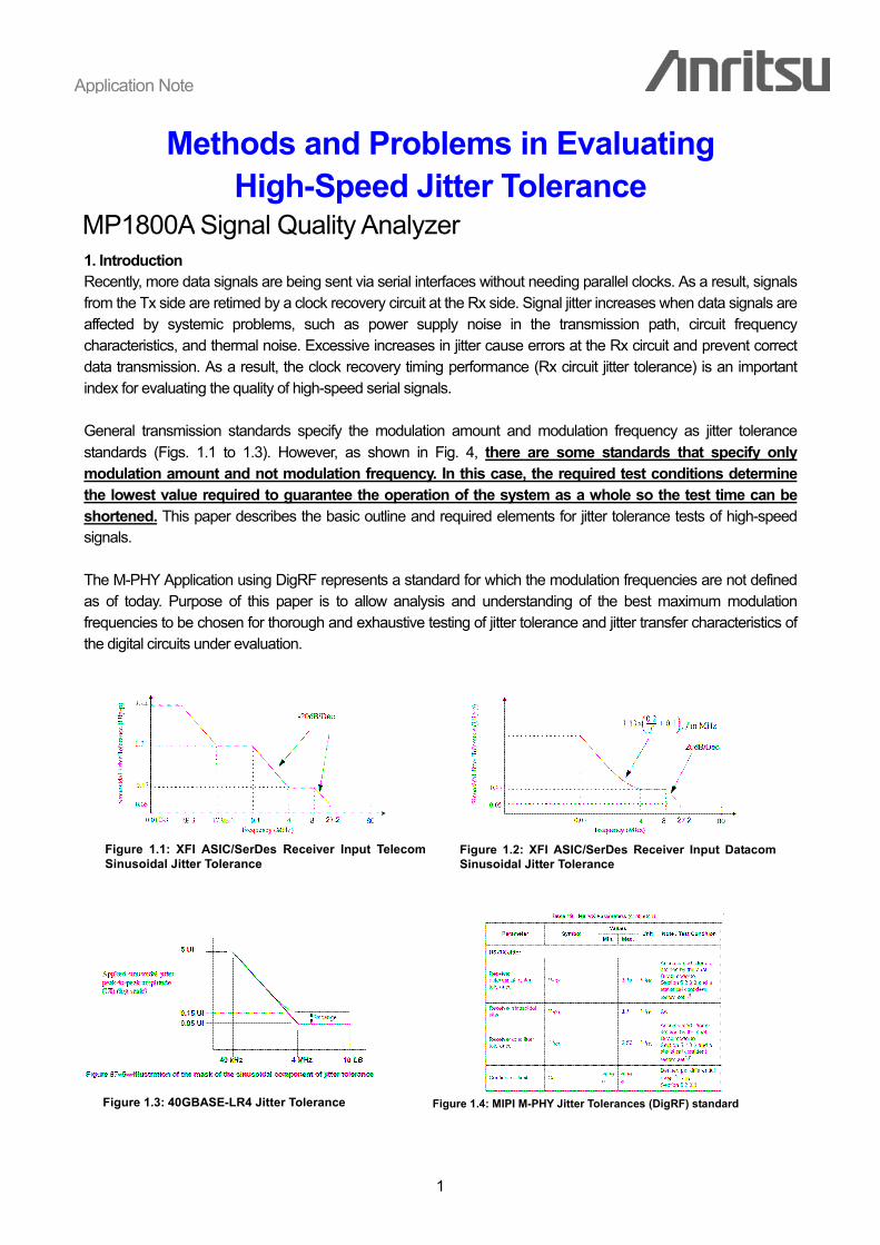
1. Introduction Recently, more data signals are being sent via serial interfaces without needing parallel clocks. As a result, signals from the Tx side are retimed by a clock recovery circuit at the Rx side. Signal jitter increases when data signals are affected by systemic problems, such as power supply noise in the transmission path, circuit frequency characteristics, and thermal noise. Excessive increases in jitter cause errors at the Rx circuit and prevent correct data transmission. As a result, the clock recovery timing performance (Rx circuit jitter tolerance) is an important index for evaluating the quality of high-speed serial signals. General transmission standards specify the modulation amount and modulation frequency as jitter tolerance standards (Figs. 1.1 to 1.3). However, as shown in Fig. 4, there are some standards that specify only modulation amount and not modulation frequency. In this case, the required test conditions determine the lowest value required to guarantee the operation of the system as a whole so the test time can be shortened. This paper describes the basic outline and required elements for jitter tolerance tests of high-speed signals. The M-PHY Application using DigRF represents a standard for which the modulation frequencies are not defined as of today. Purpose of this paper is to allow analysis and understanding of the best maximum modulation frequencies to be chosen for thorough and exhaustive testing of jitter tolerance and jitter transfer characteristics of the digital circuits under evaluation.
Figure 1.1: XFI ASIC/SerDes Receiver Input TelecomSinusoidal Jitter Tolerance
Figure 1.2: XFI ASIC/SerDes Receiver Input Datacom Sinusoidal Jitter Tolerance
Figure 1.3: 40GBASE-LR4 Jitter Tolerance
Figure 1.4: MIPI M-PHY Jitter Tolerances (DigRF) standard
Application Note
MP1800A Signal Quality Analyzer

2
2. Clock Recovery Outline As mentioned above, serial transmission use clock recovery technologies. Generally, clock recovery uses an internal PLL (Phase Locked Loop) circuit (Fig. 2.1).
Reference Signal
Loop Filter
VCOPhase Detector
1/N Clock Output
Fig. 2.1: PLL Block Diagram A specific Loop bandwidth is designated for the PLL circuit and the VCO phase noise is suppressed to the same level as the reference signal by the PLL negative feedback in the Loop bandwidth. When the loop bandwidth is wide, the VCO covers a wider phase noise range, shortening the PLL lock time. When the input signal phase noise characteristics are worse than the VCO, the phase noise reference signal is amplified N times. In general, the PLL band is set to minimize clock output jitter. Figure 2.2 shows the clock recovery circuit.
Input Data Signal
Loop Filter
VCOPhase Detector
Data Output
D-FF
Figure 2.2: Clock Recovery Circuit
Like the PLL circuit, the loop bandwidth is designated for the basic clock recovery circuit. When the loop bandwidth is wide, the jitter tolerance is good and the clock recovery circuit lock time is shortened. On the other hand, more jitter propagates to the circuit after clock recovery. If there are several overlapping wide-loop-bandwidth clock-recovery circuits, more jitter accumulates in the latter levels and the system operation becomes unstable as a whole. ITU-T standards for transmission equipment such as SDH and SONET specify system quality by regulating the amount of jitter that the device itself generates (jitter generation), the jitter transmission characteristics to the next level (jitter transfer) and the error-free data retiming characteristics (jitter tolerance). To improve the overall jitter quality, jitter transfer specifies the smallest permissible amount of jitter transferred to the next level, and jitter tolerance specifies the tolerance to jitter transferred from the previous level. The SDH/SONET technology not only uses a high-Q narrowband PLL but also uses a low-Q, wideband SAW filter. In general, the jitter tolerance of a narrowband circuit is reduced and jitter is not transferred easily to the next level. On the other hand, the jitter tolerance of a wideband circuit is increased and more jitter is transferred to the next level. In a system containing a mixture of circuits with these two types of characteristics, it is necessary to design the circuits so that as little as possible jitter generated from the widest bandwidth parts is transferred to the next level. As a result, the SDH/SONET technology specifies tests at up to 10 times the PLL bandwidth to cover the SAW filter band.
The following section explains errors due to jitter in the clock recovery circuit. In an optical module with built-in clock recovery circuit, optical signals are retimed at the clock recovery circuit after O/E conversion. As mentioned, clock recovery uses a unique standards-defined loop bandwidth. When the input data signal jitter is within the loop bandwidth, the recovered clock follows the data signal jitter and no error occurs (Fig. 2.3-c). However, if the input data signal jitter is outside the loop bandwidth, the recovered clock jitter is
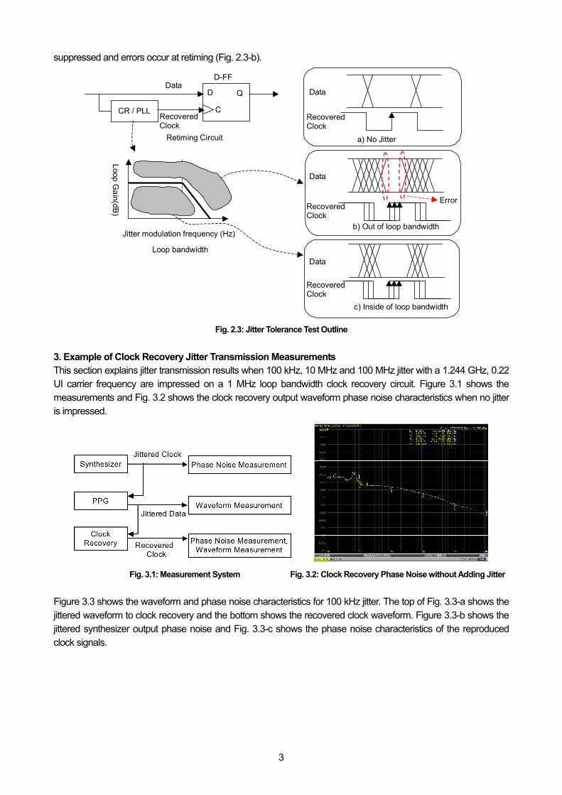
3
suppressed and errors occur at retiming (Fig. 2.3-b).
D-FF
D
C
Q
CR / PLL
Jitter modulation frequency (Hz)
Loop Gain(dB)
a) No Jitter
c) Inside of loop bandwidth
b) Out of loop bandwidth
Error
Data
Recovered Clock
Data
RecoveredClock
Data
RecoveredClock
Data
RecoveredClock
Retiming Circuit
Loop bandwidth
Fig. 2.3: Jitter Tolerance Test Outline
3. Example of Clock Recovery Jitter Transmission Measurements This section explains jitter transmission results when 100 kHz, 10 MHz and 100 MHz jitter with a 1.244 GHz, 0.22 UI carrier frequency are impressed on a 1 MHz loop bandwidth clock recovery circuit. Figure 3.1 shows the measurements and Fig. 3.2 shows the clock recovery output waveform phase noise characteristics when no jitter is impressed.
Fig. 3.1: Measurement System Fig. 3.2: Clock Recovery Phase Noise without Adding Jitter
Figure 3.3 shows the waveform and phase noise characteristics for 100 kHz jitter. The top of Fig. 3.3-a shows the jittered waveform to clock recovery and the bottom shows the recovered clock waveform. Figure 3.3-b shows the jittered synthesizer output phase noise and Fig. 3.3-c shows the phase noise characteristics of the reproduced clock signals.
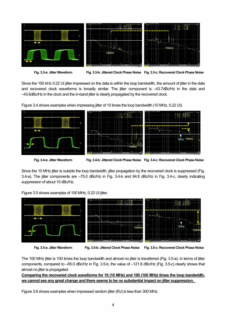
4
Fig. 3.3-a: Jitter Waveform Fig. 3.3-b: Jittered Clock Phase Noise Fig. 3.3-c: Recovered Clock Phase Noise
Since the 100 kHz 0.22 UI jitter impressed on the data is within the loop bandwidth, the amount of jitter in the data and recovered clock waveforms is broadly similar. The jitter component is –43.7dBc/Hz in the data and –43.6dBc/Hz in the clock and the in-band jitter is clearly propagated by the recovered clock. Figure 3.4 shows examples when impressing jitter of 10 times the loop bandwidth (10 MHz, 0.22 UI).
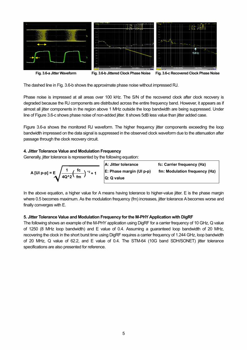
Fig. 3.4-a: Jitter Waveform Fig. 3.4-b: Jittered Clock Phase Noise Fig. 3.4-c: Recovered Clock Phase Noise
Since the 10 MHz jitter is outside the loop bandwidth, jitter propagation by the recovered clock is suppressed (Fig. 3.4-a). The jitter components are –75.0 dBc/Hz in Fig. 3.4-b and 84.8 dBc/Hz in Fig. 3.4-c, clearly indicating suppression of about 10 dBc/Hz. Figure 3.5 shows examples of 100 MHz, 0.22 UI jitter.
Fig. 3.5-a: Jitter Waveform Fig. 3.5-b: Jittered Clock Phase Noise Fig. 3.5-c: Recovered Clock Phase Noise
The 100 MHz jitter is 100 times the loop bandwidth and almost no jitter is transferred (Fig. 3.5-a). In terms of jitter components, compared to –65.0 dBc/Hz in Fig. 3.5-b, the value of –121.6 dBc/Hz (Fig. 3.5-c) clearly shows that almost no jitter is propagated. Comparing the recovered clock waveforms for 10 (10 MHz) and 100 (100 MHz) times the loop bandwidth, we cannot see any great change and there seems to be no substantial impact on jitter suppression. Figure 3.6 shows examples when impressed random jitter (RJ) is less than 300 MHz.
100kHz
100kHz
10MHz
10MHz
1MHz
100MHz100MHz 1MHz
5
Fig. 3.6-a Jitter Waveform Fig. 3.6-b Jittered Clock Phase Noise Fig. 3.6-c Recovered Clock Phase Noise
The dashed line in Fig. 3.6-b shows the approximate phase noise without impressed RJ. Phase noise is impressed at all areas over 100 kHz. The S/N of the recovered clock after clock recovery is degraded because the RJ components are distributed across the entire frequency band. However, it appears as if almost all jitter components in the region above 1 MHz outside the loop bandwidth are being suppressed. Under line of Figure 3.6-c shows phase noise of non-added jitter. It shows 5dB less value than jitter added case. Figure 3.6-a shows the monitored RJ waveform. The higher frequency jitter components exceeding the loop bandwidth impressed on the data signal is suppressed in the observed clock waveform due to the attenuation after passage through the clock recovery circuit. 4. Jitter Tolerance Value and Modulation Frequency Generally, jitter tolerance is represented by the following equation:
√ A [UI p-p] = E 1 4Q^2
fc fm
^2 + 1 )(A: Jitter tolerance fc: Carrier frequency (Hz) E: Phase margin (UI p-p) fm: Modulation frequency (Hz)Q: Q value
In the above equation, a higher value for A means having tolerance to higher-value jitter. E is the phase margin where 0.5 becomes maximum. As the modulation frequency (fm) increases, jitter tolerance A becomes worse and finally converges with E. 5. Jitter Tolerance Value and Modulation Frequency for the M-PHY Application with DigRF The following shows an example of the M-PHY application using DigRF for a carrier frequency of 10 GHz, Q value of 1250 (8 MHz loop bandwidth) and E value of 0.4. Assuming a guaranteed loop bandwidth of 20 MHz, recovering the clock in the short burst time using DigRF requires a carrier frequency of 1.244 GHz, loop bandwidth of 20 MHz, Q value of 62.2, and E value of 0.4. The STM-64 (10G band SDH/SONET) jitter tolerance specifications are also presented for reference.
1MHz
6
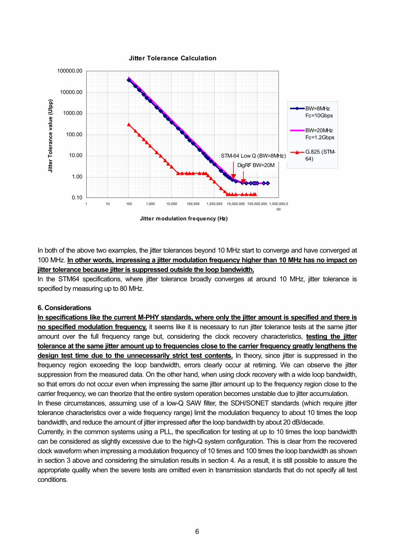
Jitter Tolerance Calculation
0.10
1.00
10.00
100.00
1000.00
10000.00
100000.00
1 10 100 1,000 10,000 100,000 1,000,000 10,000,000 100,000,000 1,000,000,000
Jitter modulation frequency (Hz)
Jitte
r Tol
eran
ce v
alue
(UIp
p)
BW=8MHzFc=10Gbps
BW=20MHzFc=1.2Gbps
G.825 (STM-64)STM-64 Low Q (BW=8MHz)
DigRF BW=20M
In both of the above two examples, the jitter tolerances beyond 10 MHz start to converge and have converged at 100 MHz. In other words, impressing a jitter modulation frequency higher than 10 MHz has no impact on jitter tolerance because jitter is suppressed outside the loop bandwidth. In the STM64 specifications, where jitter tolerance broadly converges at around 10 MHz, jitter tolerance is specified by measuring up to 80 MHz. 6. Considerations In specifications like the current M-PHY standards, where only the jitter amount is specified and there is no specified modulation frequency, it seems like it is necessary to run jitter tolerance tests at the same jitter amount over the full frequency range but, considering the clock recovery characteristics, testing the jitter tolerance at the same jitter amount up to frequencies close to the carrier frequency greatly lengthens the design test time due to the unnecessarily strict test contents. In theory, since jitter is suppressed in the frequency region exceeding the loop bandwidth, errors clearly occur at retiming. We can observe the jitter suppression from the measured data. On the other hand, when using clock recovery with a wide loop bandwidth, so that errors do not occur even when impressing the same jitter amount up to the frequency region close to the carrier frequency, we can theorize that the entire system operation becomes unstable due to jitter accumulation. In these circumstances, assuming use of a low-Q SAW filter, the SDH/SONET standards (which require jitter tolerance characteristics over a wide frequency range) limit the modulation frequency to about 10 times the loop bandwidth, and reduce the amount of jitter impressed after the loop bandwidth by about 20 dB/decade. Currently, in the common systems using a PLL, the specification for testing at up to 10 times the loop bandwidth can be considered as slightly excessive due to the high-Q system configuration. This is clear from the recovered clock waveform when impressing a modulation frequency of 10 times and 100 times the loop bandwidth as shown in section 3 above and considering the simulation results in section 4. As a result, it is still possible to assure the appropriate quality when the severe tests are omitted even in transmission standards that do not specify all test conditions.

7
7. Summary This paper describes the following from the viewpoint of a measuring instrument manufacturer. (a) When the clock recovery loop bandwidth is wide, jitter accumulates at the next level and the whole system may become unstable. (b) Attenuated jitter does not propagate easily outside the clock recovery loop bandwidth. (c) Even in jitter tolerance standards that do not specify the modulation frequency, it is sufficient to test at jitter covering the clock recovery loop band of the system design. Anritsu continues to provide excellent measurement solutions to improve product quality and added value.
References IEEE P802.3ba D3.0 INF-8077i 10 Gigabit Small Form Factor Pluggable Module Rev. 4.5 MIPI Alliance Specification for M-PHY Version 0.71 ITU-T Recommendation G.825 Proposal for Optical Module Test Method to improve Yield and Increase Throughput, “Anritsu Document” Japanese Patent Office Publication of patent applications Japanese published unexamined application 5-56029 Code conversion circuit

Reference: Derivation of Jitter Tolerance The CDR circuit jitter tolerance is approximated by the following model.
NRZ Signal
Jitter amount: J(fj)
Clock Recovery
Jitter Gain: G(fj)
D Q Recovered NRZ Signal
DF/F
The following conditions are set for the error-free data recovery:
J(fj) - J(fj) x G(fj) < E J(fj): Jitter of data signal J(fj) x G(fj): Jitter of Clock Recovery Circuit E: Jitter margin (Generally 1/2 UIp-p) G(fj): (Generally 0 to 1)
J(fj) < (1)
E 1 - G(fj)
Jmax(fj) is the minimum input jitter amount exceeding (1). This is defined by the jitter tolerance of the CDR circuit and G(fj) is defined by the primary RC filter. When fj → 0, Jmax(fj) tends to ∞ and when fj → ∞, Jmax(fj) converges with E.
fc fcfj fj
E
G(fj) Jmax(fj)
-20dB/DEC
Become infinite
<Jmax(fj) Calculation> Considering RC Filter as G(fj)
R
C Vi Vo
Vo(ω) = jωC
1
jωC1R +
Vi(ω) = 1 + jωRC 1
Vi(ω)
G(ω) = = Vo(ω)Vi(ω) 1 + jωRC
1
Jmax(ω) = = = {1 – j ( )} E (2)E1 - G(ω)
1 + jωRC1
E
1 -jωC
1
The Q value of the PLL resonator circuit using this RC filter as the Loop filter is found from the following equation:
Jmax(fj) is found by substituting Eq. (3) into Eq. (2).
Jmax(ω) = {1 – j ( )} E
ω2Qωo
Jmax(ω) = 1 + ( )^2 ・ E = E・ ( )^2 + 1 [Uip-p] ω2Q ωo√ √4Q^2
1 fj
fo
//
http://www.anritsu.com
5-1-1 Onna, Atsugi-shi, Kanagawa, 243-8555Phone : +81 46 223-1111
No. MP1800A-Jitter_Tolerance-E-F-1-(1.00) Printed in Japan 2010-1 PRS