application note 1. tdps3500e0e10 half-bridge evaluation ... · tdps3500e0e10 1 04/04/2016...
TRANSCRIPT

TDPS3500E0E10
1 04/04/2016
Application Note
1. TDPS3500E0E10 Half-Bridge Evaluation Board
1.1 Introduction
This half-bridge evaluation board provides the elements of a simple buck or boost converter for
basic study of switching characteristics and efficiency achievable with Transphorm’s 650V GaN
power switches. In either buck or boost mode the circuit can be configured for synchronous
rectification. Jumpers allow use of a single logic input or separate hi/lo inputs. The high-voltage
input and output can operate at up to 400Vdc, with a power output of up to 3.5kW. The inductor
provided is intended for efficient operation at 100kHz, although other inductors and other
frequencies may be easily used.
Fig. 1. Half-Bridge Evaluation Board

TDPS3500E0E10
2 04/04/2016
1.2 TDPS3500E0E10 Input/output Specifications:
• High-voltage input/output: 400 Vdc maximum
• Auxiliary Supply (J1): 10V min, 18V max
• Logic inputs: nominal 0-5V;
for the pulse-generation circuit, Vlo < 1.5V, Vhi> 3.0V
for direct connection to gate driver, Vlo < 0.8V, Vhi > 2.0V
SMA coaxial connectors
• Switching frequency: configuration dependent
lower limit determined by peak inductor current
upper limit determined by desired dead time and power dissipation
• Power dissipation in HEMTs is limited by maximum junction temperature. Refer to the
TPH3205WS data sheet.
1.3 Circuit Description
The circuit comprises a simple half bridge featuring two TPH3205WS GaN power transistors, as
indicated in the block diagram of Figure 2. Two high-voltage ports are provided which can serve
as either input or output, depending on the configuration: boost or buck. In either case one
transistor acts as the active power switch while the other carries the freewheeling current. The
latter device may be enhanced, as a synchronous rectifier, or not. With GaN power transistors
the reverse recovery charge is low and there is no need for additional freewheeling diodes. Two
input connectors are provided which can be connected to sources of logic-level command signals
for the hi/lo gate driver. Both inputs may be driven by off-board signal sources, or alternatively,
a single signal source may be connected to an on-board pulse-generator circuit which generates
the two non-overlapping pulses. Jumpers determine how the input signals are used.
An inductor is provided as a starting point for investigation. This is a 330uH toroid intended to
demonstrate a reasonable compromise between size and efficiency for power up to 3.5kW at a
switching frequency of 100kHz.

TDPS3500E0E10
3 04/04/2016
Figure 2: Functional Block Diagram
1.4 Using the board
The board can be used for evaluation of basic switching functionality in a variety of circuit
configurations. It is not a complete circuit, but rather a building block. It can be used in steady-
state DC/DC converter mode with output power up to 3.5kW.
1.5 Configurations
Figure 3 shows the basic power connections for buck and boost modes. For buck mode, the
HVdc input (terminals J2, J3) is connected to the high-voltage supply and the output is taken
from terminals J5 and J7. For boost mode the connections are reversed.
Note that in boost mode a load must be connected. The load current affects the output voltage up
to the transition from DCM to CCM. In buck mode the load may be an open circuit.

TDPS3500E0E10
4 04/04/2016
(a) Buck Mode
(b) Boost mode
Figure 3. Supply and Load connections for Buck (a) and Boost (b) configurations.
TDPS3500E0E10
5 04/04/2016
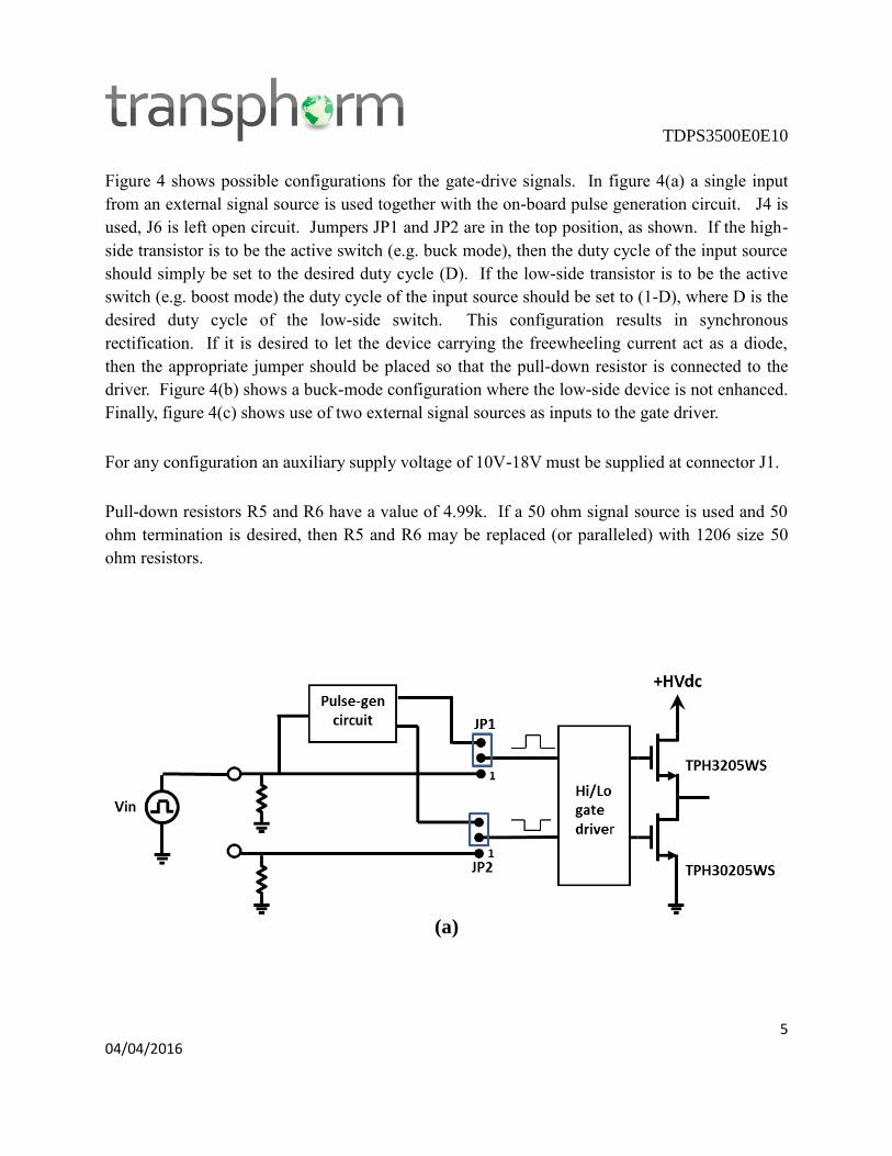
Figure 4 shows possible configurations for the gate-drive signals. In figure 4(a) a single input
from an external signal source is used together with the on-board pulse generation circuit. J4 is
used, J6 is left open circuit. Jumpers JP1 and JP2 are in the top position, as shown. If the high-
side transistor is to be the active switch (e.g. buck mode), then the duty cycle of the input source
should simply be set to the desired duty cycle (D). If the low-side transistor is to be the active
switch (e.g. boost mode) the duty cycle of the input source should be set to (1-D), where D is the
desired duty cycle of the low-side switch. This configuration results in synchronous
rectification. If it is desired to let the device carrying the freewheeling current act as a diode,
then the appropriate jumper should be placed so that the pull-down resistor is connected to the
driver. Figure 4(b) shows a buck-mode configuration where the low-side device is not enhanced.
Finally, figure 4(c) shows use of two external signal sources as inputs to the gate driver.
For any configuration an auxiliary supply voltage of 10V-18V must be supplied at connector J1.
Pull-down resistors R5 and R6 have a value of 4.99k. If a 50 ohm signal source is used and 50
ohm termination is desired, then R5 and R6 may be replaced (or paralleled) with 1206 size 50
ohm resistors.
(a)

TDPS3500E0E10
6 04/04/2016
(b)
(c)
Figure 4: input configurations. (a) using a single source for either buck or boost mode (b) buck mode
without synchronous rectification (c) using two signal sources
1.6 Deadtime control
The required form of the gate-drive signals is shown in Figure 5. The times marked A are the
deadtimes when neither transistor is driven on. The deadtime must be greater than zero to avoid
shoot-through currents. The Si8230BB gate drive chip ensures a minimum deadtime based on

TDPS3500E0E10
7 04/04/2016
the value of resistor R7, connected to the DT input. The deadtime in ns is equal to the resistance
in kohm x 10: so the default value of 12k corresponds to 120ns. This will add to any deadtime
already present in the input signals. The on-board pulse generator circuit, for example, creates
deadtimes of about the 60ns. The resulting deadtime at the gate pins of Q1 and Q2 is about
240ns. Either shorting or removing R7 will reduce the deadtime to 60ns.
Figure 5: Non-overlapping gate pulses
1.7 Design details
The detailed circuit schematic is included with this file as a pdf. The parts list follows in table 1.
Qty Value Package ID Manf Manf P/N
1 HS1 Cool
Innovations 3-242411MS73377
1 74LVC1G17
DBV U3
Texas Instruments SN74LVC1G17DBVR
1 DIODE-DO-
214AC D1
Fairchild ES1J
6 2.2uF 450V ECW-
FD2W225J C9, C18, C26, C27,
C28, C29 Panasonic ECW-FD2W225J
2 0 R-
US_R0603 R11, R12
Vishay MCT06030Z0000ZP500
2 JP2E JP1, JP2 FCI 68001-403HLF
4 KEYSTONE_
7691 J2, J3, J5, J7
Keystone 7691
1 LT3082 U1 Linear
Technology LT3082EST#PBF
1 330uH 330uH
inductor L1
CWS PI 12-18-157
1 .1u C-EUC1812 C7 Kemet C1812V104KDRACTU
7 .1u C-USC0603 C10, C11, C12, C14,
C20, C21, C22 AVX 06033C104JAT2A

TDPS3500E0E10
8 04/04/2016
6 .1u C-
USC2225K C8, C16, C17, C30,
C31, C32 Vishay VJ2225Y104KXGAT
1 12k R-
US_R0603 R7
Rohm ESR03EZPF1202
1 0 R-
US_R1206 R9
Panasonic ERJ-8GEY0R00V
1 10 R-
US_R0805 R4
Panasonic ERJ-6GEYJ100V
4 15 R-
US_R1206 R13, R14, R15, R16
Rohm RNCP1206FTD15R0
2 100pF C-USC0603 C19, C23 AVX 06035A101FAT2A
1 10MEG R-
US_R1206 R3
Stackpole HVCB1206FKC10M0
2 10u C-EUC0805 C13, C15 Kemet C0805C106M4PACTU
2 1k R-
US_R0603 R8, R10
Yageo RC0603FR-071KL
1 1u C-EUC0805 C2 Yageo CC0805ZRY5V8BB105
1 2.2u C-EUC0805 C3 TDK C2012X5R1E225K125AC
1 22-23-2021 22-23-2021 J1 Molex 22-23-2021
1 22u C-USC1206 C1 TDK C3225X7R1C226K250AC
2 47p C-USC1210 C24, C25 Vishay VJ1210A470JXGAT5ZL
3 4.7n C-EUC1206 C4, C5, C6 Kemet C1206C472KDRACTU
3 4.99k R-
US_R1206 R1, R5, R6
Stackpole RMCF1206FT4K99
1 499k R-
US_R1206 R2
Stackpole RMCF1206FT499K
2 74AHC1G86DBV 74AHC1G86
DBV U4, U5
Texas Instruments SN74AHC1G86DBVR
2 BAT54W BAT54W D2, D3 NXP BAT54W
2 BU-SMA-G BU-SMA-G J4, J6 Molex 731000114
1 SI8230 SI8230 U2 Silicon Labs SI8230BB-B-IS1
2 TPH3205WS TPH3205W
S Q1, Q2
Transphorm TPH3205WS
2 TPSPAD1-13 TPSPAD1-
13 TP1, TP3, TP2, TP4,
TP5 Keystone 5001K
1 PCB
AR LeadFree Solder MG
CHEMICALS 4900-454G
1 Q1 insulator (high side)
Aavid Thermalloy
4169G
TDPS3500E0E10
9 04/04/2016
2 plastic shoulder
washers
7721-7PPSG
4 standoffs TBD
1 12V, 24"
red/black cable
Molex 22012025 + 0008500135
or equiv.
Table 1. Bill of Materials for the half-bridge Evaluation Board
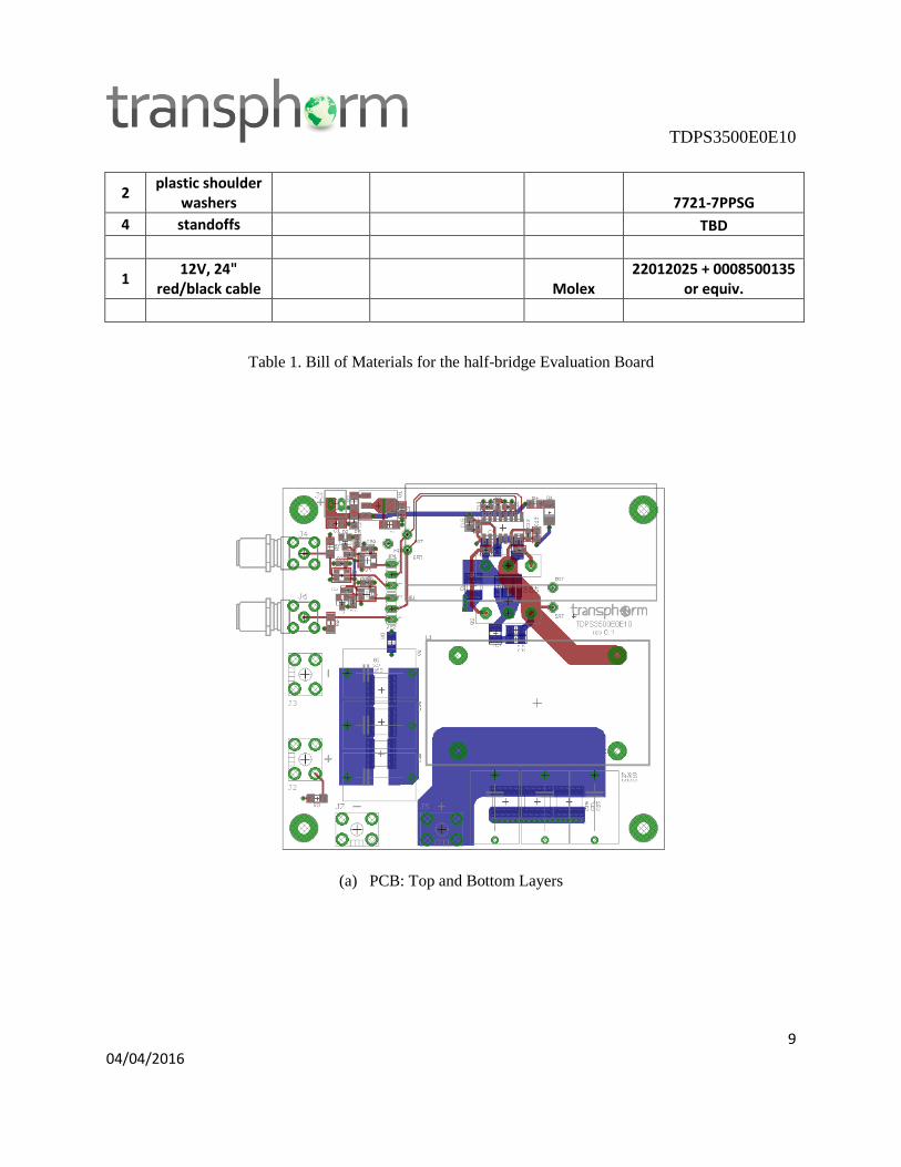
(a) PCB: Top and Bottom Layers

TDPS3500E0E10
10 04/04/2016
(b) PCB: Inner Layer 2, Ground Plane
(c) PCB: Inner Layer 3: Power Plane

TDPS3500E0E10
11 04/04/2016
Figure 7: PCB layers
1.7 Probing
Plated-through holes labeled test points 4 and 5 (TP4, TP5) are provided for probing the
switching waveform. In order to minimize inductance during measurement, the tip and the
ground of the probe should be directly attached to the sensing points to minimize the sensing
loop. For safe, reliable and accurate measurement, a scope probe tip may be directly soldered to
TP4 and a short ground wire soldered to TP5. Figure 8 indicates an alternative which does not
require soldering the probe tip.
WARNINGS:
There is no specific protection against over-current or over-voltage on this board.
If the on-board pulse generation circuit is used in boost mode, a zero input corresponds to 100%
duty cycle for the active low-side switch.
Fig. 8. Low-inductance probing of fast, high-voltage signals

TDPS3500E0E10
12 04/04/2016
Efficiency has been measured for this circuit in boost mode with 200Vdc in and 400Vdc out,
switching at 100kHz.
Figure 9: efficiency for a boost 200V:400V converter
0
10
20
30
40
50
60
97
97.2
97.4
97.6
97.8
98
98.2
98.4
98.6
98.8
99
0 500 1000 1500 2000 2500 3000 3500 4000
Loss
(W
)
Effi
cie
ncy
(%
)
Power (W)
50kHz 100kHz