half-bridge driver ic - nxp semiconductors | automotive ... · latch-up free and robust half bridge...
TRANSCRIPT

1. General description
The UBA2080(A) and UBA2081 are high voltage monolithic integrated circuits made using the latch-up free Silicon-On-Insulator (SOI) process. The circuit is designed for driving MOSFETs in a half-bridge configuration.
2. Features and benefits
Latch-up free and robust half bridge driver
Output driver capability: IO(sink) = 400 mA and IO(source) = 200 mA
Maximum frequency 800 kHz
UBA2080:
Outputs in phase with HIN and LIN inputs
Overlap protection
UBA2081:
Outputs in phase with CLK input
Adjustable dead-time
Low active shutdown input
3. Applications
Driver (via external MOSFETs) for any kind of load in a half-bridge configuration
UBA2080A:
Selectable between UBA2080 and UBA2081 functionality
Thermally enhanced package for high frequency operation.
4. Ordering information
UBA2080; UBA2080A; UBA2081Half-bridge driver ICRev. 3 — 18 June 2012 Product data sheet
Table 1. Ordering information
Type number Package
Name Description Version
UBA2080P DIP8 plastic dual in-line package; 8 leads SOT97-1
UBA2081P
UBA2080T SO8 plastic small outline package; 8 leads SOT96-1
UBA2081T
UBA2080AT SO14 plastic small outline package; 14 leads SOT108-1

NXP Semiconductors UBA2080; UBA2080A; UBA2081Half-bridge driver IC
5. Block diagram
Refer to Figure 7 and Figure 8 for detailed information on the required application components.
Fig 1. Block diagram (UBA2080 and UBA2080A with select = GND)
LOGIC
SEL
ULVO ULVO HS DRIVER
FS
SH
GHVDD
LEVEL SHIFTER
LS DRIVER
OVERLAPPROTECTION
R1R2 S
GND
GL
aaa-001102
LIN
HIN
Fig 2. Block diagram (UBA2080A and UBA2081 with select = VDD)
LOGIC
NON-OVERLAP
ULVO ULVO HS DRIVER
FS
SH
GHVDD
SD
SEL
Vref
CLK LEVEL SHIFTER
LS DRIVER
R1R2 S
GND
GL
aaa-001107
UBA2080_UBA2081 All information provided in this document is subject to legal disclaimers. © NXP B.V. 2012. All rights reserved.
Product data sheet Rev. 3 — 18 June 2012 2 of 15

NXP Semiconductors UBA2080; UBA2080A; UBA2081Half-bridge driver IC
6. Pinning information
6.1 Pinning
6.2 Pin description
Fig 3. UBA2080: Pin configuration DIP8 and SO8 package
Fig 4. UBA2080A: Pin configuration SO14 package
Fig 5. UBA2081: Pin configuration DIP8 and SO8 package
UBA2080
VDD GL
GND SH
LIN GH
HIN FS
aaa-001121
1
2
3
4
6
5
8
7
aaa-001134
UBA2080A
GND SEL
GND GND
SD/LIN VDD
GND GL
CLK/HIN GND
FS GND
GH SH
1
2
3
4
5
6
7 8
10
9
12
11
14
13
UBA2081
VDD GL
GND SH
SD GH
CLK FS
aaa-001126
1
2
3
4
6
5
8
7
Table 2. Pin description UBA2080/UBA2081 DIP8 and SO8
Symbol Pin Description
UBA2080 (DIP8/SO8)
UBA2081 (DIP8/SO8)
VDD 1 IC supply
GND 2 IC ground and low-side driver return
LIN 3 - low-side driver logic input
SD - 3 low active analog shutdown input and non-overlap time setting
HIN 4 - high-side driver logic input
CLK - 4 clock logic input
FS 5 floating supply voltage
GH 6 high-side MOSFET gate
SH 7 high-side MOSFET source
GL 8 low-side MOSFET gate
Table 3. Pin description UBA2080AT (SO14)
Symbol Pin Description
GND 1, 2, 4, 9, 10, 13 IC ground and low side driver return
SD/LIN 3 low-side driver logic input or low active shutdown and non-overlap time setting
CLK/HIN 5 high-side driver logic input or clock logic input
FS 6 floating supply voltage
SH 8 high-side MOSFET source
UBA2080_UBA2081 All information provided in this document is subject to legal disclaimers. © NXP B.V. 2012. All rights reserved.
Product data sheet Rev. 3 — 18 June 2012 3 of 15

NXP Semiconductors UBA2080; UBA2080A; UBA2081Half-bridge driver IC
7. Functional description
7.1 Start-up state
The IC enters the start-up state when the supply voltage on pin VDD increases. In the start-up state, the high-side power transistor is non-conducting and the low-side power transistor is switched on. The internal circuit is reset and the capacitor on the bootstrap pin FS is charged. The start-up state is defined until the value of VDD = the VDD(start) value. After which the IC switches to the oscillation state.
The circuit enters the start-up state again when the voltage on pin VDD < VDD(stop).
7.2 UBA2080 oscillation state
In the oscillation state, the output voltage of the GL and GH drivers depend on the logical signals HIN and LIN (see Table 4).
To prevent cross conduction in the half-bridge MOSFETs, the combination HIN = LIN = 1 is not allowed. Both GL and GH are LOW under this condition.
7.3 UBA2081 oscillation state
In the oscillation state, the output voltage of the GL and GH drivers depend on the logical signals CLK and SD (see Table 5).
GH 7 high-side MOSFET gate
GL 11 low-side MOSFET gate
VDD 12 IC supply
SEL 14 select UBA2080 or UBA2081 functionality; only connect to GND or VDD
Table 3. Pin description UBA2080AT (SO14) …continued
Symbol Pin Description
Table 4. UBA2080 Logic table
State HIN LIN GH GL
Start-up - - LOW HIGH
Oscillation 0 0 LOW LOW
Oscillation 0 1 LOW HIGH
Oscillation 1 0 HIGH LOW
Oscillation 1 1 LOW LOW
Table 5. UBA2081 Logic table
State CLK SD GH GL
Start-up - - LOW HIGH
Oscillation 0 0 LOW HIGH
Oscillation 1 0 HIGH LOW
Oscillation 0 1 LOW LOW
Oscillation 1 1 LOW LOW
UBA2080_UBA2081 All information provided in this document is subject to legal disclaimers. © NXP B.V. 2012. All rights reserved.
Product data sheet Rev. 3 — 18 June 2012 4 of 15

NXP Semiconductors UBA2080; UBA2080A; UBA2081Half-bridge driver IC
7.4 UBA2081 non-overlap time
The external resistor (RSD) on pin SD sets the non-overlap time of the UBA2081. The relationship between this resistor value and actual dead-time is listed in Figure 6.
It is essential to add a 10 nF to 100 nF decoupling capacitor across RSD to ensure a noise immune dead-time system.
7.5 UBA2081 shutdown protection
When the voltage at pin SD is pulled below VIH, the internal sink drivers of the pins GL and GH are immediately enabled to switch off the external power MOSFETs.
The shutdown comparator has a hysteresis of Vhys(SD) to avoid multiple switching.
Preferably, pin SD is pulled low via a collector of a transistor (see application schematic) to avoid loading of this pin (Influences the non-overlap time settings) at normal operation.
7.6 UBA2080 overlap protection
The internal logic takes care that the GL driver and GH driver are both set to LOW in this situation to avoid that HIN = LIN = 1 causes a cross current in the external half-bridge.
7.7 UBA2080A select function
Pin SEL enables the selection of either the UBA2080 or the UBA2081 functionality. SEL = 0 gives the UBA2080 functionality. SEL = VDD gives the UBA2081 functionality.
Fig 6. Non-overlap time versus SD resistor (RSD)
0 1 2 3
aaa-001135
1000
2000
3000
tno(ns)
0RSD (MΩ)
UBA2080_UBA2081 All information provided in this document is subject to legal disclaimers. © NXP B.V. 2012. All rights reserved.
Product data sheet Rev. 3 — 18 June 2012 5 of 15

NXP Semiconductors UBA2080; UBA2080A; UBA2081Half-bridge driver IC
8. Limiting values
[1] In accordance with the Human Body Model (HBM): equivalent to discharging a 100 pF capacitor through a 1.5 kΩ series resistor.
[2] In accordance with the Machine Model (MM): equivalent to discharging a 200 pF capacitor through a 1.5 kΩ series resistor and a 0.75 μH inductor.
9. Thermal characteristics
[1] In accordance with IEC 60747-1.
Table 6. Limiting valuesIn accordance with the Absolute Maximum Rating System (IEC 60134).
Symbol Parameter Conditions Min Max Unit
VDD supply voltage nominal 0 15.5 V
VFS voltage on pin FS VSH VSH + 15.5 V
VSH voltage on pin SH source high-side MOSFET −3 +600 V
t < 1 μs −14 +600 V
Vi(HIN) input voltage on pin HIN logic input for high-side driver 0 15.5 V
Vi(LIN) input voltage on pin LIN logic input for low-side driver 0 15.5 V
Vi(SEL) input voltage on pin SEL 0 15.5 V
VCLK voltage on pin CLK logic input for output drivers 0 15.5 V
Vi(SD) input voltage on pin SD logic input for output drivers and analog input for non-overlap setting
0 15.5 V
SR slew rate on pin SH; repetitive −6 +6 V/ns
Tj junction temperature −40 +150 °C
Tamb ambient temperature −40 +150 °C
Tstg storage temperature −55 +150 °C
VESD electrostatic discharge voltage
human body model: [1]
pins FS, GH and SH - 1 kV
pins VDD, HIN, LIN, SD, CLK, SEL - 2 kV
machine model: [2]
all pins - 250 V
Table 7. Thermal characteristics
Symbol Parameter Conditions Typ Unit
SO8
Rth(j-a) thermal resistance from junction to ambient in free air [1] 160 K/W
SO14 and DIP8
Rth(j-a) thermal resistance from junction to ambient in free air [1] 100 K/W
UBA2080_UBA2081 All information provided in this document is subject to legal disclaimers. © NXP B.V. 2012. All rights reserved.
Product data sheet Rev. 3 — 18 June 2012 6 of 15

NXP Semiconductors UBA2080; UBA2080A; UBA2081Half-bridge driver IC
10. Characteristics
Table 8. CharacteristicsTj = 25 °C; all voltages are measured with respect to SGND; VDD = 12.8 V; positive currents flow into the IC.
Symbol Parameter Conditions Min Typ Max Unit
High-voltage supply
Ileak leakage current FS = GH = SH = 600 V - - 10 μA
Start-up state
IVDD current on pin VDD 420 520 620 μA
VDD(start) start supply voltage 11 12 13 V
VDD(stop) stop supply voltage 8 8.5 9 V
VDD(hys) hysteresis of supply voltage start-to-stop 3 3.5 4 V
Pin LIN input
VIH HIGH-level input voltage 1.6 2.2 2.8 V
Vhys(LIN) hysteresis voltage on pin LIN - 400 - mV
II(LIN) input current on pin LIN - 0 1 μA
Pin HIN input
VIH HIGH-level input voltage 1.6 2.2 2.8 V
Vhys(HIN) hysteresis voltage on pin HIN - 400 - mV
II(HIN) input current on pin HIN - 0 1 μA
Pin CLK input
VIH HIGH-level input voltage 2.7 - - V
VIL LOW-level input voltage - - 0.8 V
II(CLK) input current on pin CLK - 0 1 μA
Pin SD input
VIH HIGH-level input voltage to activate shutdown 1.6 2.2 2.8 V
Vhys(SD) hysteresis voltage on pin SD - 400 - mV
tno non-overlap time RSD = 100 kΩ; typical minimum - 140 - ns
RSD = 3 MΩ; typical maximum - 2.4 - μs
Pin SEL input
II(SEL) input current on pin SEL - 0 1 μA
gate drivers
IO(source) output source current VFS = VVDD = 12 V; VSH = 0 V; VGH = VGL = 8 V
- 200 - mA
IO(sink) output sink current VFS = VVDD = 12 V; VSH = 0 V; VGH = VGL = 4 V
- 400 - mA
Vd(bs) bootstrap diode voltage Id(bs) = 20 mA - 2.3 - V
VUVLO undervoltage lockout voltage reset 3.6 4.2 4.8 V
IFS current on pin FS VFS = VVDD = 12 V; VSH = 0 V 27 32 37 μA
Timing
tPD propagation delay UBA2080; matching; C(GL) = C(GH) = 0, propagation time difference between GL and GH.
- 50 - ns
UBA2080_UBA2081 All information provided in this document is subject to legal disclaimers. © NXP B.V. 2012. All rights reserved.
Product data sheet Rev. 3 — 18 June 2012 7 of 15

NXP Semiconductors UBA2080; UBA2080A; UBA2081Half-bridge driver IC
11. Application information
tPD(LIN-GL) propagation delay from LIN to GL
UBA2080; C(GL) = 0 pF - 240 - ns
tPD(HIN-GH) propagation delay from HIN to GH
UBA2080; C(GH) = 0 pF - 180 - ns
fmax maximum frequency 800 - - kHz
Table 8. Characteristics …continuedTj = 25 °C; all voltages are measured with respect to SGND; VDD = 12.8 V; positive currents flow into the IC.
Symbol Parameter Conditions Min Typ Max Unit
Fig 7. Typical UBA2080 application
Remark: The capacitor connected to the SD pin ensures a noise immune dead-time.
Fig 8. Typical UBA2081 application
UBA2080
from μC
FS
GH
to loadSH
HIN
LIN
GL
HVIN
CFS
CVDD
aaa-001424
VDDVDD supply
GND
UBA2081input clock
shutdown
FS
GH
to loadSH
SD
CLK
GL
GND
HVIN
CFS
CVDD
tno
aaa-001425
VDDVDD supplyRSD
UBA2080_UBA2081 All information provided in this document is subject to legal disclaimers. © NXP B.V. 2012. All rights reserved.
Product data sheet Rev. 3 — 18 June 2012 8 of 15

NXP Semiconductors UBA2080; UBA2080A; UBA2081Half-bridge driver IC
12. Package outline
Fig 9. Package outline SOT96-1 (SO8)
UNITA
max. A1 A2 A3 bp c D(1) E(2) (1)e HE L Lp Q Zywv θ
REFERENCESOUTLINEVERSION
EUROPEANPROJECTION ISSUE DATE
IEC JEDEC JEITA
mm
inches
1.750.250.10
1.451.25
0.250.490.36
0.250.19
5.04.8
4.03.8
1.276.25.8
1.050.70.6
0.70.3 8
0
o
o
0.25 0.10.25
DIMENSIONS (inch dimensions are derived from the original mm dimensions)
Notes
1. Plastic or metal protrusions of 0.15 mm (0.006 inch) maximum per side are not included.
2. Plastic or metal protrusions of 0.25 mm (0.01 inch) maximum per side are not included.
1.00.4
SOT96-1
X
w M
θ
AA1
A2
bp
D
HE
Lp
Q
detail X
E
Z
e
c
L
v M A
(A )3
A
4
5
pin 1 index
1
8
y
076E03 MS-012
0.0690.0100.004
0.0570.049
0.010.0190.014
0.01000.0075
0.200.19
0.160.15
0.050.2440.228
0.0280.024
0.0280.012
0.010.010.041 0.0040.0390.016
0 2.5 5 mm
scale
SO8: plastic small outline package; 8 leads; body width 3.9 mm SOT96-1
99-12-2703-02-18
UBA2080_UBA2081 All information provided in this document is subject to legal disclaimers. © NXP B.V. 2012. All rights reserved.
Product data sheet Rev. 3 — 18 June 2012 9 of 15

NXP Semiconductors UBA2080; UBA2080A; UBA2081Half-bridge driver IC
Fig 10. Package outline SOT97-1 (DIP8)
REFERENCESOUTLINEVERSION
EUROPEANPROJECTION ISSUE DATE
IEC JEDEC JEITA
SOT97-199-12-2703-02-13
UNIT Amax.
1 2 b1(1) (1) (1)
b2 c D E e M ZHL
mm
DIMENSIONS (inch dimensions are derived from the original mm dimensions)
A min.
A max. b
max.wMEe1
1.731.14
0.530.38
0.360.23
9.89.2
6.486.20
3.603.05
0.2542.54 7.628.257.80
10.08.3
1.154.2 0.51 3.2
inches 0.0680.045
0.0210.015
0.0140.009
1.070.89
0.0420.035
0.390.36
0.260.24
0.140.12
0.010.1 0.30.320.31
0.390.33
0.0450.17 0.02 0.13
b2
050G01 MO-001 SC-504-8
MH
c
(e )1
ME
A
L
seat
ing
plan
e
A1
w Mb1
e
D
A2
Z
8
1
5
4
b
E
0 5 10 mm
scale
Note
1. Plastic or metal protrusions of 0.25 mm (0.01 inch) maximum per side are not included.
pin 1 index
DIP8: plastic dual in-line package; 8 leads (300 mil) SOT97-1
UBA2080_UBA2081 All information provided in this document is subject to legal disclaimers. © NXP B.V. 2012. All rights reserved.
Product data sheet Rev. 3 — 18 June 2012 10 of 15

NXP Semiconductors UBA2080; UBA2080A; UBA2081Half-bridge driver IC
Fig 11. Package outline SOT108-1 (SO14)
UNITA
max. A1 A2 A3 bp c D(1) E(1) (1)e HE L Lp Q Zywv θ
REFERENCESOUTLINEVERSION
EUROPEANPROJECTION ISSUE DATE
IEC JEDEC JEITA
mm
inches
1.750.250.10
1.451.25
0.250.490.36
0.250.19
8.758.55
4.03.8
1.276.25.8
0.70.6
0.70.3 8
0
o
o
0.25 0.1
DIMENSIONS (inch dimensions are derived from the original mm dimensions)
Note
1. Plastic or metal protrusions of 0.15 mm (0.006 inch) maximum per side are not included.
1.00.4
SOT108-1
X
w M
θ
AA1
A2
bp
D
HE
Lp
Q
detail X
E
Z
e
c
L
v M A
(A )3
A
7
8
1
14
y
076E06 MS-012
pin 1 index
0.0690.0100.004
0.0570.049
0.010.0190.014
0.01000.0075
0.350.34
0.160.15
0.05
1.05
0.0410.2440.228
0.0280.024
0.0280.012
0.01
0.25
0.01 0.0040.0390.016
99-12-2703-02-19
0 2.5 5 mm
scale
SO14: plastic small outline package; 14 leads; body width 3.9 mm SOT108-1
UBA2080_UBA2081 All information provided in this document is subject to legal disclaimers. © NXP B.V. 2012. All rights reserved.
Product data sheet Rev. 3 — 18 June 2012 11 of 15
NXP Semiconductors UBA2080; UBA2080A; UBA2081Half-bridge driver IC
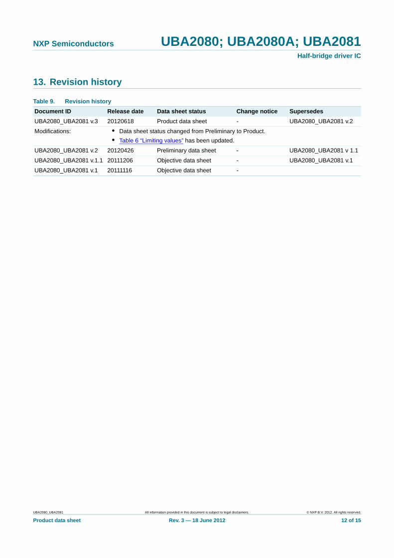
13. Revision history
Table 9. Revision history
Document ID Release date Data sheet status Change notice Supersedes
UBA2080_UBA2081 v.3 20120618 Product data sheet - UBA2080_UBA2081 v.2
Modifications: • Data sheet status changed from Preliminary to Product.
• Table 6 “Limiting values” has been updated.
UBA2080_UBA2081 v.2 20120426 Preliminary data sheet - UBA2080_UBA2081 v 1.1
UBA2080_UBA2081 v.1.1 20111206 Objective data sheet - UBA2080_UBA2081 v.1
UBA2080_UBA2081 v.1 20111116 Objective data sheet -
UBA2080_UBA2081 All information provided in this document is subject to legal disclaimers. © NXP B.V. 2012. All rights reserved.
Product data sheet Rev. 3 — 18 June 2012 12 of 15

NXP Semiconductors UBA2080; UBA2080A; UBA2081Half-bridge driver IC
14. Legal information
14.1 Data sheet status
[1] Please consult the most recently issued document before initiating or completing a design.
[2] The term ‘short data sheet’ is explained in section “Definitions”.
[3] The product status of device(s) described in this document may have changed since this document was published and may differ in case of multiple devices. The latest product status information is available on the Internet at URL http://www.nxp.com.
14.2 Definitions
Draft — The document is a draft version only. The content is still under internal review and subject to formal approval, which may result in modifications or additions. NXP Semiconductors does not give any representations or warranties as to the accuracy or completeness of information included herein and shall have no liability for the consequences of use of such information.
Short data sheet — A short data sheet is an extract from a full data sheet with the same product type number(s) and title. A short data sheet is intended for quick reference only and should not be relied upon to contain detailed and full information. For detailed and full information see the relevant full data sheet, which is available on request via the local NXP Semiconductors sales office. In case of any inconsistency or conflict with the short data sheet, the full data sheet shall prevail.
Product specification — The information and data provided in a Product data sheet shall define the specification of the product as agreed between NXP Semiconductors and its customer, unless NXP Semiconductors and customer have explicitly agreed otherwise in writing. In no event however, shall an agreement be valid in which the NXP Semiconductors product is deemed to offer functions and qualities beyond those described in the Product data sheet.
14.3 Disclaimers
Limited warranty and liability — Information in this document is believed to be accurate and reliable. However, NXP Semiconductors does not give any representations or warranties, expressed or implied, as to the accuracy or completeness of such information and shall have no liability for the consequences of use of such information. NXP Semiconductors takes no responsibility for the content in this document if provided by an information source outside of NXP Semiconductors.
In no event shall NXP Semiconductors be liable for any indirect, incidental, punitive, special or consequential damages (including - without limitation - lost profits, lost savings, business interruption, costs related to the removal or replacement of any products or rework charges) whether or not such damages are based on tort (including negligence), warranty, breach of contract or any other legal theory.
Notwithstanding any damages that customer might incur for any reason whatsoever, NXP Semiconductors’ aggregate and cumulative liability towards customer for the products described herein shall be limited in accordance with the Terms and conditions of commercial sale of NXP Semiconductors.
Right to make changes — NXP Semiconductors reserves the right to make changes to information published in this document, including without limitation specifications and product descriptions, at any time and without notice. This document supersedes and replaces all information supplied prior to the publication hereof.
Suitability for use — NXP Semiconductors products are not designed, authorized or warranted to be suitable for use in life support, life-critical or safety-critical systems or equipment, nor in applications where failure or malfunction of an NXP Semiconductors product can reasonably be expected to result in personal injury, death or severe property or environmental damage. NXP Semiconductors and its suppliers accept no liability for inclusion and/or use of NXP Semiconductors products in such equipment or applications and therefore such inclusion and/or use is at the customer’s own risk.
Applications — Applications that are described herein for any of these products are for illustrative purposes only. NXP Semiconductors makes no representation or warranty that such applications will be suitable for the specified use without further testing or modification.
Customers are responsible for the design and operation of their applications and products using NXP Semiconductors products, and NXP Semiconductors accepts no liability for any assistance with applications or customer product design. It is customer’s sole responsibility to determine whether the NXP Semiconductors product is suitable and fit for the customer’s applications and products planned, as well as for the planned application and use of customer’s third party customer(s). Customers should provide appropriate design and operating safeguards to minimize the risks associated with their applications and products.
NXP Semiconductors does not accept any liability related to any default, damage, costs or problem which is based on any weakness or default in the customer’s applications or products, or the application or use by customer’s third party customer(s). Customer is responsible for doing all necessary testing for the customer’s applications and products using NXP Semiconductors products in order to avoid a default of the applications and the products or of the application or use by customer’s third party customer(s). NXP does not accept any liability in this respect.
Limiting values — Stress above one or more limiting values (as defined in the Absolute Maximum Ratings System of IEC 60134) will cause permanent damage to the device. Limiting values are stress ratings only and (proper) operation of the device at these or any other conditions above those given in the Recommended operating conditions section (if present) or the Characteristics sections of this document is not warranted. Constant or repeated exposure to limiting values will permanently and irreversibly affect the quality and reliability of the device.
Terms and conditions of commercial sale — NXP Semiconductors products are sold subject to the general terms and conditions of commercial sale, as published at http://www.nxp.com/profile/terms, unless otherwise agreed in a valid written individual agreement. In case an individual agreement is concluded only the terms and conditions of the respective agreement shall apply. NXP Semiconductors hereby expressly objects to applying the customer’s general terms and conditions with regard to the purchase of NXP Semiconductors products by customer.
No offer to sell or license — Nothing in this document may be interpreted or construed as an offer to sell products that is open for acceptance or the grant, conveyance or implication of any license under any copyrights, patents or other industrial or intellectual property rights.
Document status[1][2] Product status[3] Definition
Objective [short] data sheet Development This document contains data from the objective specification for product development.
Preliminary [short] data sheet Qualification This document contains data from the preliminary specification.
Product [short] data sheet Production This document contains the product specification.
UBA2080_UBA2081 All information provided in this document is subject to legal disclaimers. © NXP B.V. 2012. All rights reserved.
Product data sheet Rev. 3 — 18 June 2012 13 of 15

NXP Semiconductors UBA2080; UBA2080A; UBA2081Half-bridge driver IC
Export control — This document as well as the item(s) described herein may be subject to export control regulations. Export might require a prior authorization from competent authorities.
Non-automotive qualified products — Unless this data sheet expressly states that this specific NXP Semiconductors product is automotive qualified, the product is not suitable for automotive use. It is neither qualified nor tested in accordance with automotive testing or application requirements. NXP Semiconductors accepts no liability for inclusion and/or use of non-automotive qualified products in automotive equipment or applications.
In the event that customer uses the product for design-in and use in automotive applications to automotive specifications and standards, customer (a) shall use the product without NXP Semiconductors’ warranty of the
product for such automotive applications, use and specifications, and (b) whenever customer uses the product for automotive applications beyond NXP Semiconductors’ specifications such use shall be solely at customer’s own risk, and (c) customer fully indemnifies NXP Semiconductors for any liability, damages or failed product claims resulting from customer design and use of the product for automotive applications beyond NXP Semiconductors’ standard warranty and NXP Semiconductors’ product specifications.
14.4 TrademarksNotice: All referenced brands, product names, service names and trademarks are the property of their respective owners.
15. Contact information
For more information, please visit: http://www.nxp.com
For sales office addresses, please send an email to: [email protected]
UBA2080_UBA2081 All information provided in this document is subject to legal disclaimers. © NXP B.V. 2012. All rights reserved.
Product data sheet Rev. 3 — 18 June 2012 14 of 15

NXP Semiconductors UBA2080; UBA2080A; UBA2081Half-bridge driver IC
16. Contents
1 General description . . . . . . . . . . . . . . . . . . . . . . 1
2 Features and benefits . . . . . . . . . . . . . . . . . . . . 1
3 Applications . . . . . . . . . . . . . . . . . . . . . . . . . . . . 1
4 Ordering information. . . . . . . . . . . . . . . . . . . . . 1
5 Block diagram . . . . . . . . . . . . . . . . . . . . . . . . . . 2
6 Pinning information. . . . . . . . . . . . . . . . . . . . . . 36.1 Pinning . . . . . . . . . . . . . . . . . . . . . . . . . . . . . . . 36.2 Pin description . . . . . . . . . . . . . . . . . . . . . . . . . 3
7 Functional description . . . . . . . . . . . . . . . . . . . 47.1 Start-up state . . . . . . . . . . . . . . . . . . . . . . . . . . 47.2 UBA2080 oscillation state. . . . . . . . . . . . . . . . . 47.3 UBA2081 oscillation state . . . . . . . . . . . . . . . . 47.4 UBA2081 non-overlap time . . . . . . . . . . . . . . . 57.5 UBA2081 shutdown protection . . . . . . . . . . . . . 57.6 UBA2080 overlap protection. . . . . . . . . . . . . . . 57.7 UBA2080A select function . . . . . . . . . . . . . . . . 5
8 Limiting values. . . . . . . . . . . . . . . . . . . . . . . . . . 6
9 Thermal characteristics . . . . . . . . . . . . . . . . . . 6
10 Characteristics. . . . . . . . . . . . . . . . . . . . . . . . . . 7
11 Application information. . . . . . . . . . . . . . . . . . . 8
12 Package outline . . . . . . . . . . . . . . . . . . . . . . . . . 9
13 Revision history. . . . . . . . . . . . . . . . . . . . . . . . 12
14 Legal information. . . . . . . . . . . . . . . . . . . . . . . 1314.1 Data sheet status . . . . . . . . . . . . . . . . . . . . . . 1314.2 Definitions. . . . . . . . . . . . . . . . . . . . . . . . . . . . 1314.3 Disclaimers . . . . . . . . . . . . . . . . . . . . . . . . . . . 1314.4 Trademarks. . . . . . . . . . . . . . . . . . . . . . . . . . . 14
15 Contact information. . . . . . . . . . . . . . . . . . . . . 14
16 Contents . . . . . . . . . . . . . . . . . . . . . . . . . . . . . . 15
© NXP B.V. 2012. All rights reserved.
For more information, please visit: http://www.nxp.comFor sales office addresses, please send an email to: [email protected]
Date of release: 18 June 2012
Document identifier: UBA2080_UBA2081
Please be aware that important notices concerning this document and the product(s)described herein, have been included in section ‘Legal information’.