apple iie technical notes
TRANSCRIPT
Apple IIe#1: Overview of the Apple IIe 1 of 1
Apple IITechnical Notes
Developer Technical SupportApple IIe#1: Overview of the Apple IIe
Revised by: Matt Deatherage November 1988Revised by: Cameron Birse October 1985
This Technical Note formerly presented an overview of the Apple IIe.
This Note formerly presented an overview of the Apple IIe and its differences from the Apple ][and ][+. The Apple IIe Technical Reference Manual now documents this information, as well asdifferences with other members of the Apple II family.
Further Reference• Apple IIe Technical Reference Manual
Apple IIe#2: Hardware Protocol for Doing DMA 1 of 9
Apple IITechnical Notes
Developer Technical SupportApple IIe#2: Hardware Protocol for Doing DMA
Revised by: Glenn A. Baxter & Rob Moore November 1988Written by: Peter Baum January 1983
This Technical Note explains the hardware protocol for doing direct memory access (DMA) onthe Apple IIe and Apple ][ and is meant as a guideline for developing peripherals which do DMAon these machines, not as a specification for future Apple products or revisions.
This Note covers the timing differences between the Apple ][ and IIe and also gives tips on howto design a peripheral card that will work in both systems. The reader should be very familiarwith either the Apple ][+ or the Apple IIe, especially the timing on the data and address buses inrelation to the 6502.
DMA is used by peripheral cards in the Apple II family to transfer data directly into memorywithout benefit of the processor. Transfer of data from a peripheral device into RAM cannormally be handled one byte at a time under control of the processor. By using DMA, you canachieve greater data transfer rates than the 6502 can handle in software. This transfer rate canapproach the full-cycle time of the memory. This technique can also be used to transfer singledata bytes into memory without requiring the CPU to process an interrupt, which can be verytime consuming.
The DMA process entails five steps: turn the processor off, gain access to the R/W* line andboth address and data buses, complete the data transfer, release the data and address buses, andfinally, allow the microprocessor to restart. This Note covers each of these steps in detail.
At this point, I should caution the prospective developer that DMA on an Apple ][+ or Apple IIecan only be done under certain circumstances. Because DMA turns off the processor, anyprogram with a software timing loop will not work properly. These programs assume that eachinstruction will take a fixed amount of time, which is not true when the processor stops in themiddle of an instruction. This assumption means that the Apple II disk drives will not worksince they require a timing loop to read a disk. (Co-processor cards work with DMA becausethey initiate the disk access and know that DMA cannot be used until the disk is finished).
Another problem is that because of the mapping scheme used on the Apple IIe extended 80-column (64K) card, a peripheral card cannot tell which memory bank is being used without acomplicated detection scheme. This problem means that if a DMA device writes to a certainmemory space, it might not be able to read the same data back.
Apple II Technical Notes
2 of 9 Developer Technical Support
6502
A
E0-
FF
RO
M64
KR
AM
80 C
OL.
AU
X R
AM
DA
TA
LA
TC
H
MM
UIO
U
DA
TA
LAT
CH
VID
EO
CIR
CU
ITS
TIM
ING
CIR
CU
ITS
7 4 L S 2 4 4
KE
YB
OA
RD TIM
ING
AN
D C
ON
TR
OL
SIG
NA
LS
AD
DR
ES
S B
US
( A
0 -
A15
)
EX
TE
RN
AL
DA
TA
B
US
MD
IN/O
UT
VID
EO
DA
TA
RA
M A
DD
R B
US
(0
-7)
KB
D
RO
ME
N
INT
ER
NA
L D
AT
A B
US
(M
D 0
-7)
Fig
ure
1–A
pple
IIe
Fun
ctio
nal B
lock
Dia
gram
74LS
245
PE
RIP
HE
RA
L S
LOT
S
November 1988
Apple IIe#2: Hardware Protocol for Doing DMA 3 of 9
Though the differences between the Apple IIe and Apple ][+ architecture appear to be significantto a device which uses DMA, this should not affect the design in most cases. A good rule ofthumb is that if a device is designed to work on the Apple IIe, then it will be backwardcompatible and also run on the Apple ][+. The converse is not true; cards that use DMA on theApple ][+ might not work on the Apple IIe, hence, most of the descriptions in this Note refer tothe Apple IIe with occasional references to the Apple ][+. For example, the timing specificationslisted are calculated from the Apple IIe timing paths unless otherwise noted.
Occasionally the descriptions refer to a chip on the motherboard of the Apple IIe, so a set ofApple IIe schematics should be nearby. The corresponding parts on the Apple ][+ will bespecified when applicable.
The following paragraphs describe and define some of the terms that are used throughout thisNote. The Apple IIe block diagram on the previous page may be helpful when reading about thebuses.
01 (phase one) time The time when the 01 system timing signal is high. During this time thedata bus, address bus, and RAM are used for video refreshing. This timeis also called the video cycle or video phase.
0o (phase zero) time The time when 0o clock is high. 0o is the inverse of 01. During this timethe microprocessor uses the data and address buses. This time is alsoknown as the CPU cycle or CPU phase.
IOU and MMU Two MOS custom chips inside the Apple IIe. See chapter 7 of the AppleIIe Technical Reference Manual for more details on the custom chips.
Data bus The microprocessor, ROM, and RAM are connected to this bus. On theIIe this bus generally has MOS components connected to it rather thanTTL and is sometimes called the MOS data bus. A 74LS245 bidirectionalbus transceiver (location B2 on the original motherboard) connects thisinternal bus to an external bus that the outside world sees through theperipheral slots. The data bus connected to the peripheral slots is calledthe external data bus. The Apple ][ does not have these two data buses.Instead, the peripheral slots are connected to the ROM, CPU data buffers,and RAM data inputs. The RAM data outputs are multiplexed with thekeyboard data onto this bus.
Address bus There are three different sections to the address bus on the Apple IIe. Thefirst section consists of the addresses from the 6502A into a pair of74LS244s (locations B1,B3). Part two connects the other side of the ’244to the address bus that the peripheral slots see. Also connected on this busare the MMU, the ROM, and the chips that decode I/O SELECT,DEVICE SELECT, and I/O STROBE. The third address bus isgenerated by the custom chips and is only used to access the RAM. TheMMU and IOU automatically multiplex this bus with the high byte andlow byte of an address during any RAM access, whether it be for videorefresh or for a microprocessor instruction fetch. This third bus is calledthe RAM address bus. The Apple ][ also has these three buses, but uses8T97s and discrete logic instead of the 74LS244 and custom chips.
Apple II Technical Notes
4 of 9 Developer Technical Support
6502 microprocessor In the Apple IIe a 6502A, a 2 MHz part is used instead of the 1 MHz 6502used in the Apple ][+. Since the custom chips in the Apple IIe are MOSand slower than the TTL in the Apple ][+, the faster 6502A was used toguarantee better margins. For example, the 6502A sets up the address busfaster on the Apple IIe than the 6502 does in the Apple ][+.

November 1988
Apple IIe#2: Hardware Protocol for Doing DMA 5 of 9
On the IIe, all the timing signals are generated by the PAL timing chip, except for the 7 M signalwhich is generated from an 74S109 or 74109 (early versions of the IIe). Although both the PALand the 74S019 use the 14 M signal for a clock, there will be some skew between edges of the 7M clock and the timing signals from the PAL, such as the edges of 0o or 01. This skew meansthe 7 M clock edge may rise as much as 20 ns before, or 5 ns after, the 0o falling edge. Theclock signals of the Apple ][+ should be tighter than this (probably within 5 ns of each other)since 7 M, 0o, and 01 are all generated from the same chip, a 74S175. Take this skew intoaccount whenever using the 7 M signal in a design.
Getting on the Bus (Exact Change Only)
1. Pull DMA low during 01 time.
On the Apple IIe, the DMA line controls the direction of the 74LS245, whichenables the internal data bus outwards to the peripheral slots or enables externaldata onto the internal bus. Changing the state of the DMA line during 0o couldcause the ’245 to change directions, forcing the internal data bus to go tri-stateduring a microprocessor read. The 6502 would read garbage and the computermight go belly up by jumping to a random memory location.
On the Apple ][, pulling the DMA line always forces the CPU data bus buffer topoint inward and drive toward the 6502. Pulling the DMA line low during 0o of awrite cycle would result in garbage being written to memory, since the data bus tothe RAM would suddenly go tri-state.
2. Wait 30 ns, then assert address bus and R/W* line.
Before driving the address bus and R/W* line, the system must process thetransition on the DMA line and release the bus. This requires:
25 ns ’LS244 output disable from low level5 ns ’S02 low to high level output transition
30 ns delay from DMA negative edge before driving address bus
The 30 ns wait will also work on the Apple ][, since it only needs 27 ns (’LS04and 8T97).
2 1
3 0
H i g h
Apple II Technical Notes
6 of 9 Developer Technical Support
Figure 2–Getting On The Bus
3. Address and R/W* line must be valid within 213 ns of 01 positive edge.
This constraint is needed to meet the setup requirements of the IOU, MMU, andRAM. This time can be derived from the 6502A (2 MHz) setup requirements.The Apple ][ can wait for 300 ns before data must be valid, because it uses the 1MHz 6502 which has a longer setup time.
Warning: This specification (the address setup time) is the major cause of failure forcards which use DMA in the Apple IIe. Many DMA cards which wereoriginally designed for the Apple ][+ do not meet this specification.
During DMA (Keep Your Hands Inside the Bus at all Times)
1. Don’t drive the data bus during 01 time.
On an Apple ][+, it is safe to drive the data bus 35 ns after asserting the R/W* linelow, regardless of the point in the timing cycle. When the R/W* line goes low,the 74LS257s at locations B6 and B7 tri-state the data bus, even in the middle of0o or 01. This action prevents a bus fight from occurring between a DMA deviceand the system.
At first glance of the Apple IIe logic schematics, it appears that a bus fight cannotoccur on the data bus. During the 01 half of a write cycle, the 74LS245 tri-statesthe data bus within 30 ns of the R/W* line being pulled low. While this doespreclude a fight from occurring on the data bus during 01, it doesn’t prevent a buscrash from occurring at the beginning of 0o. At the beginning of 0o, the 74LS245is enabled and will drive the external data bus. If the peripheral card also drivesthe data bus, there could be a horrendous bus fight, since the 74LS245 can source15 ma and sink 24 ma per line. This might cause a spike on the ground plane,which could cause a processor to reset on a co-processor card.
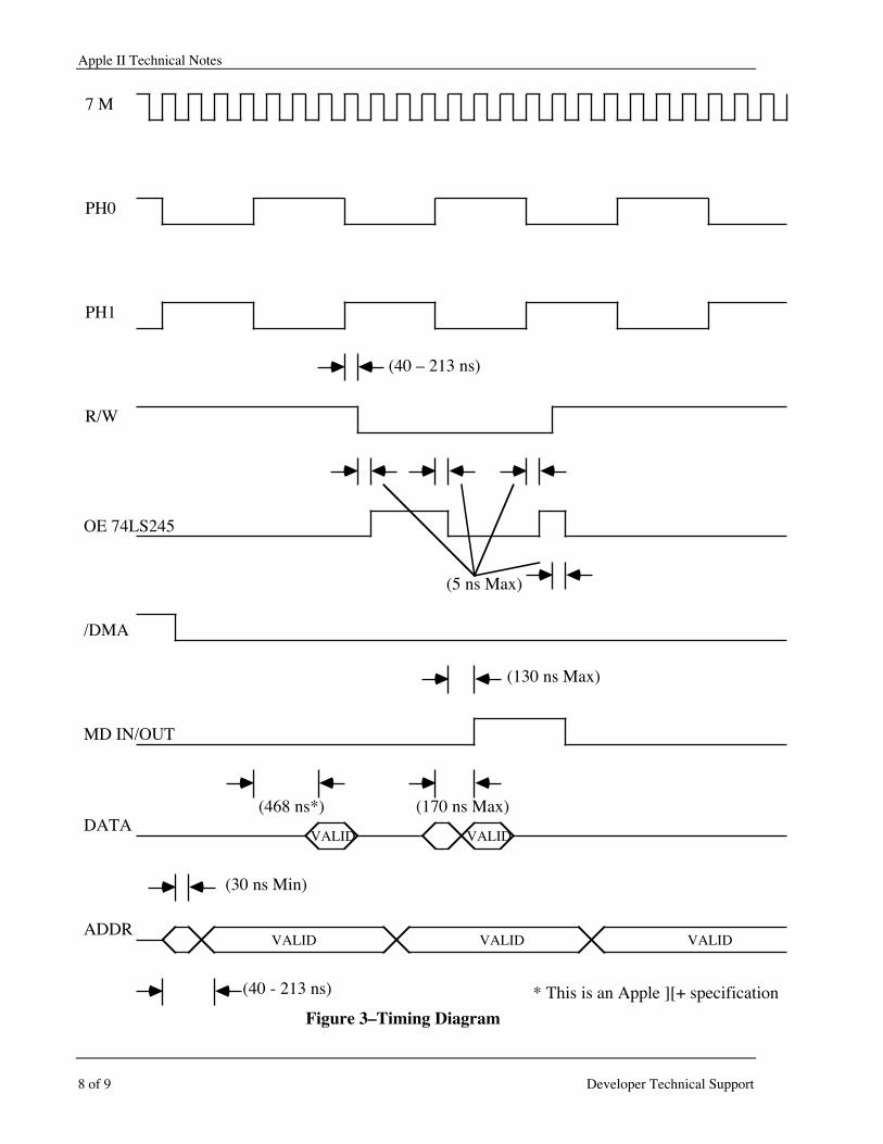
Let us take a look at the problem by stepping thru Figure 3, a timing diagram.
The diagram starts with the video cycle of a read operation. During the videocycle, the video refresh data is read from the RAM and put on the data bus. Thisvideo data will appear on the peripheral slot (external) data bus because the74LS245, as can be seen from Table 1, drives outward during 01 of a read cycle.
Typically, the address bus and R/W* line would be setup by the 6502A during 01for the next CPU cycle, but instead, a peripheral card pulls the DMA line low. Asexplained earlier, the peripheral device should wait at least 30 ns before drivingthe address bus and R/W* line. In this first DMA cycle, the peripheral card wantsto read a byte from RAM, so it keeps the R/W* line high.
November 1988
Apple IIe#2: Hardware Protocol for Doing DMA 7 of 9
At this point we must switch over and use the Apple ][+ to explain the timingrequired to read the data from RAM. The rule of thumb, that designing a DMAcard for the Apple IIe will be backward compatible and run on the Apple ][+, willnot hold here. On the Apple ][+ data is valid on the peripheral connector aminimum of 468 ns from the 0o rising edge and holds to at least the falling edgeof 0o at 490 ns. The hold time is actually the minimum propagation delay fromthe falling edge of 0o thru the following chips: 74LS257 at J1, 74LS139 at F2,74LS20 at D2, 74LS00 at A2, and finally to the enable of the 74LS257s at B5 andB6. On the Apple IIe a byte from RAM becomes valid at most 345 ns after therising edge of 0o and stays valid until the 0o falling edge.
Apple II Technical Notes
8 of 9 Developer Technical Support
OE 74LS245
/DMA
MD IN/OUT
DATA
ADDR
(40 – 213 ns)
(5 ns Max)
(130 ns Max)
(468 ns*) (170 ns Max)
(30 ns Min)
(40 - 213 ns) * This is an Apple ][+ specification
7 M
PH0
PH1
R/W
VALID VALID
VALID VALID VALID
Figure 3–Timing Diagram
November 1988
Apple IIe#2: Hardware Protocol for Doing DMA 9 of 9
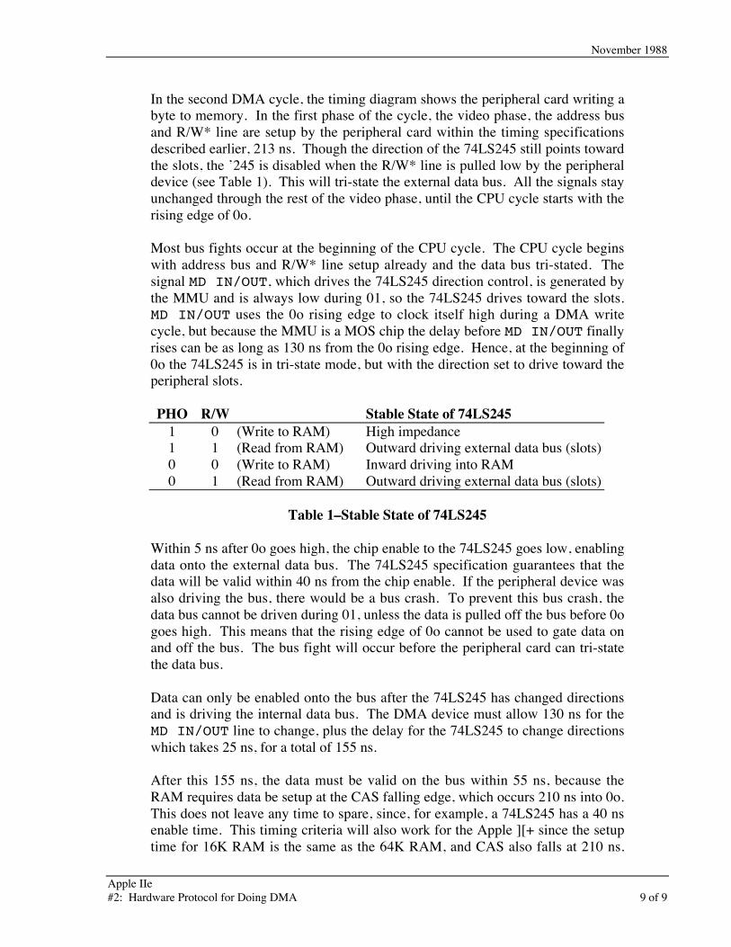
In the second DMA cycle, the timing diagram shows the peripheral card writing abyte to memory. In the first phase of the cycle, the video phase, the address busand R/W* line are setup by the peripheral card within the timing specificationsdescribed earlier, 213 ns. Though the direction of the 74LS245 still points towardthe slots, the ’245 is disabled when the R/W* line is pulled low by the peripheraldevice (see Table 1). This will tri-state the external data bus. All the signals stayunchanged through the rest of the video phase, until the CPU cycle starts with therising edge of 0o.
Most bus fights occur at the beginning of the CPU cycle. The CPU cycle beginswith address bus and R/W* line setup already and the data bus tri-stated. Thesignal MD IN/OUT, which drives the 74LS245 direction control, is generated bythe MMU and is always low during 01, so the 74LS245 drives toward the slots.MD IN/OUT uses the 0o rising edge to clock itself high during a DMA writecycle, but because the MMU is a MOS chip the delay before MD IN/OUT finallyrises can be as long as 130 ns from the 0o rising edge. Hence, at the beginning of0o the 74LS245 is in tri-state mode, but with the direction set to drive toward theperipheral slots.
PHO R/W Stable State of 74LS2451 0 (Write to RAM) High impedance1 1 (Read from RAM) Outward driving external data bus (slots)0 0 (Write to RAM) Inward driving into RAM0 1 (Read from RAM) Outward driving external data bus (slots)
Table 1–Stable State of 74LS245
Within 5 ns after 0o goes high, the chip enable to the 74LS245 goes low, enablingdata onto the external data bus. The 74LS245 specification guarantees that thedata will be valid within 40 ns from the chip enable. If the peripheral device wasalso driving the bus, there would be a bus crash. To prevent this bus crash, thedata bus cannot be driven during 01, unless the data is pulled off the bus before 0ogoes high. This means that the rising edge of 0o cannot be used to gate data onand off the bus. The bus fight will occur before the peripheral card can tri-statethe data bus.
Data can only be enabled onto the bus after the 74LS245 has changed directionsand is driving the internal data bus. The DMA device must allow 130 ns for theMD IN/OUT line to change, plus the delay for the 74LS245 to change directionswhich takes 25 ns, for a total of 155 ns.
After this 155 ns, the data must be valid on the bus within 55 ns, because theRAM requires data be setup at the CAS falling edge, which occurs 210 ns into 0o.This does not leave any time to spare, since, for example, a 74LS245 has a 40 nsenable time. This timing criteria will also work for the Apple ][+ since the setuptime for 16K RAM is the same as the 64K RAM, and CAS also falls at 210 ns.
Apple II Technical Notes
10 of 9 Developer Technical Support
The data hold time of 55 ns after CAS falls is also the same for both the Apple IIeand the Apple ][+.
Here is a scenario for a DMA write. Set up the address bus and R/W* line withinthe required 213 ns, then wait for the first 7 M (pin 36 on slot) falling edge after0o goes high before enabling your buffer onto the data bus. This edge will occurat 140 ns into 0o, and when the gate delay is added, should guarantee the bufferwill not be driving the bus in the first 155 ns. I don’t advocate depending on aminimum gate delay as standard design practice (my college professor thinkspublic whipping would be a justifiable punishment) but this is the real world (I’mnot getting graded anyway). The data bus is valid by the time CAS falls, andshould be stable for at least another 55 ns or until 0o falls.
2. The processor can be held off for a total of 10 µs. (10 0o clock cycles).
This is true if a Rockwell 6502 is being used. (A Synertek part can be held off foras long as 40 µsec.) This time is the maximum cycle time of the 6502 and if thereare no clock transitions within this time, it could result in internal registers(A,X,Y) losing data. This maximum time varies from manufacturer tomanufacturer of the 6502.
3. MMU and IOU multiplex address bus
The custom chips automatically handle the multiplexing required of the RAMaddress bus. The external device doing DMA must set up the address bus andR/W* line within 213 ns of the rising edge of 01 just like the 6502A does. Thecustom chips will automatically generate the addresses to the RAM for the videorefresh cycle during 01, but use the addresses from the address bus to set up forthe next instruction cycle. Hence, the only consideration on the address busduring DMA is to meet the 213 ns setup time requirement.
The 213 ns setup time will also work with the Apple ][ since it can take as long as300 ns to set up the address bus and R/W* line.
Getting Off the Bus
1. Don’t release DMA during 0o.
This is analogous to step 1 of Getting on the Bus. If the DMA line is releasedduring 0o the microprocessor will try to execute a cycle during this time withoutthe data or address bus set up properly. This random instruction fetch willprobably cause the system to crash.
2. Tri-state address bus drivers on peripheral slots
November 1988
Apple IIe#2: Hardware Protocol for Doing DMA 11 of 9
The DMA line is holding off the addresses from the 6502 onto the internaladdress bus by tri-stating the two 74LS244s on the Apple IIe bus and the 8T97son the Apple ][+ bus. The address bus and R/W* line from the external device inthe peripheral slots should be tri-stated before releasing the DMA line or a busfight will occur between the internal bus buffers and the peripheral slot drivers.
Apple II Technical Notes
12 of 9 Developer Technical Support
3. Release DMA line
These last two steps are the opposite of the first two steps required to get on thebus. Both of these steps, releasing the address and R/W* lines then the DMAline, should be done within 178 ns of 01 going high. This allows time for the6502A to set up the address and R/W* lines properly for the next instructioncycle.
213 ns address set up requirements5 ns ’S02 output high-to-low transition
–30 ns ’LS244 out enable time178 ns to release DMA line and allow 6502 to set up address bus
Again, the Apple ][ can take longer, up to 260 ns, before releasing the DMA line.
Further Reference• Apple IIe Technical Reference Manual
Apple IIe#3: Double High-Resolution Graphics 1 of 19
Apple IITechnical Notes
Developer Technical SupportApple IIe#3: Double High-Resolution Graphics
Revised by: Matt Deatherage, Glenn A. Baxter & Cameron Birse November 1988Written by: Peter Baum September 1983
This Technical Note is a tutorial on double high-resolution (hi-res) graphics, a feature availableon 128K Apple IIe, IIc, and IIGS computers.
Introduction
This Note was originally written in the early days of double high-resolution graphics. At thattime, there was no Apple IIc or IIGS, therefore, some of the things originally said may seem alittle strange today, five years later.
For example, this Note talks a fair amount about being sure that you have a Revision B Apple IIewith the jumper installed. All Apple IIe computers shipped since about mid-1983 have aRevision B motherboard, so this is not that big a concern anymore; furthermore, nearly every IIeout there has the aforementioned jumper already installed (it is not even an option on some third-party 80-column cards for the IIe).
Also, the IIc and IIGS are functionally equivalent (for the purposes of this article) to a Revision BIIe with the properly-jumpered 80-column card installed, and most of the references made to theApple IIe apply equally to the IIc and IIGS. We have tried to update most of the references toavoid confusion.
Considering the myriad of programming utilities, games, graphics programs, and other softwarethat now uses double high-resolution graphics, it is probable that this Note will not be as vital asit once was. If you are writing in AppleSoft BASIC, you will probably find it easier to purchasea commercial double hi-res BASIC utility package to add double hi-res commands to AppleSoft,rather than writing your own routines. Similarly, those who want double hi-res art will find adouble hi-res art application much easier than trying to draw it from the monitor or machinelanguage.
However, if you have the insatiable curiosity about these things that Apple II owners anddevelopers so often are blessed (cursed?) with, this Note will show you how double high-resolution works, as well as giving a few type-along examples in the monitor to get your feetwet.
Apple II Technical Notes
2 of 19 Developer Technical Support
This article describes the double high-resolution display mode which is available in the AppleIIc, IIGS, and the Apple IIe (with an extended 80-column card). Double hi-res graphics providestwice the horizontal resolution and more colors than the standard high-resolution mode. On amonochrome monitor, double hi-res displays 560 horizontal by 192 vertical pixels, while on acolor monitor, it allows the use of 16 colors.
Double High-Resolution on the Apple II Series
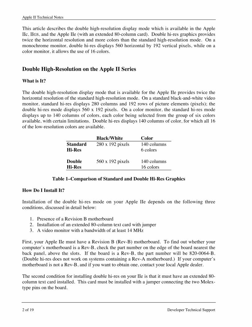
What is It?
The double high-resolution display mode that is available for the Apple IIe provides twice thehorizontal resolution of the standard high-resolution mode. On a standard black-and-white videomonitor, standard hi-res displays 280 columns and 192 rows of picture elements (pixels); thedouble hi-res mode displays 560 x 192 pixels. On a color monitor, the standard hi-res modedisplays up to 140 columns of colors, each color being selected from the group of six colorsavailable, with certain limitations. Double hi-res displays 140 columns of color, for which all 16of the low-resolution colors are available.
Black/White ColorStandard 280 x 192 pixels 140 columnsHi-Res 6 colors
Double 560 x 192 pixels 140 columnsHi-Res 16 colors
Table 1–Comparison of Standard and Double Hi-Res Graphics
How Do I Install It?
Installation of the double hi-res mode on your Apple IIe depends on the following threeconditions, discussed in detail below:
1. Presence of a Revision B motherboard2. Installation of an extended 80-column text card with jumper3. A video monitor with a bandwidth of at least 14 MHz
First, your Apple IIe must have a Revision B (Rev-B) motherboard. To find out whether yourcomputer’s motherboard is a Rev-B, check the part number on the edge of the board nearest theback panel, above the slots. If the board is a Rev-B, the part number will be 820-0064-B.(Double hi-res does not work on systems containing a Rev-A motherboard.) If your computer’smotherboard is not a Rev-B, and if you want to obtain one, contact your local Apple dealer.
The second condition for installing double hi-res on your IIe is that it must have an extended 80-column text card installed. This card must be installed with a jumper connecting the two Molex-type pins on the board.
November 1988
Apple IIe#3: Double High-Resolution Graphics 3 of 19
Warning: If your IIe has a Rev-A motherboard, do not use an extended 80-columncard with the jumper connection mentioned above; the system will notwork at all if you do.
The last requirement for operation in double hi-res mode is that your video monitor must have abandwidth of at least 14 MHz. This bandwidth is necessary because a television set that requiresa modulator will not reproduce some characters or graphic elements clearly, due to the highspeed at which the computer sends out dots in this mode. Because most of the video monitorshaving a bandwidth of up to 14 MHz are black-and-white, the working examples in this articledo not apply to color monitors. If you have a video monitor, please use it—instead of atelevision set—to display the following examples. The AppleColor composite monitors willwork just fine.

Apple II Technical Notes
4 of 19 Developer Technical Support
Your Turn to be Creative (Volunteers, Anyone?)
The tutorial that occupies the rest of this Note assumes you are working at your Apple II as youread. The second part of the lesson demonstrates the double hi-res mode; therefore, beforeembarking on the second part, you should install a jumpered extended 80-column card in yourRev-B Apple IIe (or use any Apple IIc or IIGS).
Hands-On Practice with Standard Hi-Res
The Apple II hi-res graphics display is bit-mapped. In other words, each dot on the screencorresponds to a bit in the computer’s memory. For a real-life example of bit-mapping, performthe following procedure, according to the instructions given below. (The symbol <cr> indicatesa carriage return.)
1. Boot the system.2. Engage the Caps Lock key, and type HGR<cr>. (This instruction should clear
the top of the screen.)3. Type CALL -151 <cr>. (The system is now in the monitor mode, and the
prompt should appear as an asterisk (*).)4. Type 2100:1 <cr>. One single dot should appear in the upper left-hand
corner of the screen.
Congratulations! You have just plotted your first hi-res pixel. (Not an astonishing feat, but youhave to start somewhere.)
With a black-and-white monitor, the bits in memory have a simple correspondence with the dots(pixels) on the screen. A dot of light appears if the corresponding bit is set (has a value of 1), butremains invisible if the bit is off (has a value of zero). (The dot appears white on a black-and-white monitor, and green on a green-screen monitor, such as Apple’s Monitor /// or Monitor II.For simplicity, we shall refer to an invisible dot as a black dot or pixel.) Two visible dots locatednext to each other appear as a single wide dot, and many adjacent dots appear as a line. Toobtain a display of another dot and a line, follow the steps listed below:
1. Type 2080:40 <cr>. A dot should appear above and to the right of the dotyou produced in the last exercise.
2. Type 2180:7F <cr>. A small horizontal line should appear below the first dotyou produced.
From Bits and Bytes to Pixels
The seven low-order bits in each display byte control seven adjacent dots in a row. A group of40 consecutive bytes in memory controls a row of 280 dots (7 dots per byte, multiplied by 40bytes). In the screen display, the least-significant bit of each byte appears as the leftmost pixel ina group of 7 pixels. The second least-significant bit corresponds to the pixel directly to the rightof the pixel previously displayed, and so on. To watch this procedure in action, follow the stepslisted below. The dots will appear in the middle of your screen.

November 1988
Apple IIe#3: Double High-Resolution Graphics 5 of 19
1. Type 2028:1 <cr>.2. Type 2828:2 <cr>.3. Type 3028:4 <cr>.
The three bits you specified in this exercise correspond to three pixels that are displayed oneafter another, from left to right.
The most-significant bit in each byte does not correspond to a pixel. Instead, this bit is used toshift the positions of the other seven bits in the byte. For a demonstration of this feature, followthe steps listed below:
1. Type 2050:8 <cr>.2. Type 2850:8 <cr>.3. Type 3050:8 <cr>.
You will notice that the dots align themselves vertically. Now do the following:
4. Type 2450:88 <cr>.
The new dot (that is, the one that corresponds to the bit you just specified) does not line up withthe dots you displayed earlier. Instead, it appears to be shifted one “half-dot” to the right.
5. To demonstrate that this dot really is a new dot, and not just the old dot shifted by one dotposition, type 2050:18 <cr>, 2850:18 <cr>.
You will notice that the dot mentioned under step 4 (the dot that was not aligned with the otherseven dots) is straddled by the dots above and below it. (The use of magnifying lenses ispermitted.)
Shifting the pixel one half-dot, by setting the high, most-significant bit is most often used forcolor displays. When the high bit of a byte is set to generate this shifted dot (which is also calledthe half-dot shift), then all the dots for that byte will be shifted one half dot. The half-dot shiftdoes not exist in the double hi-res mode.
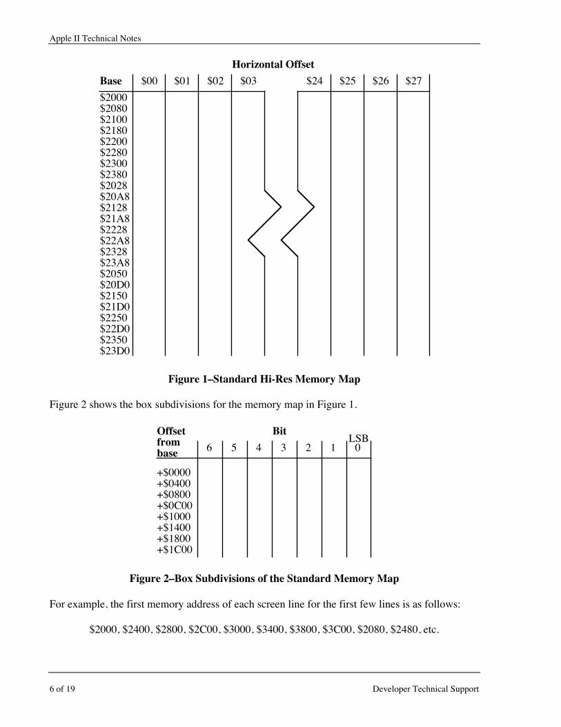
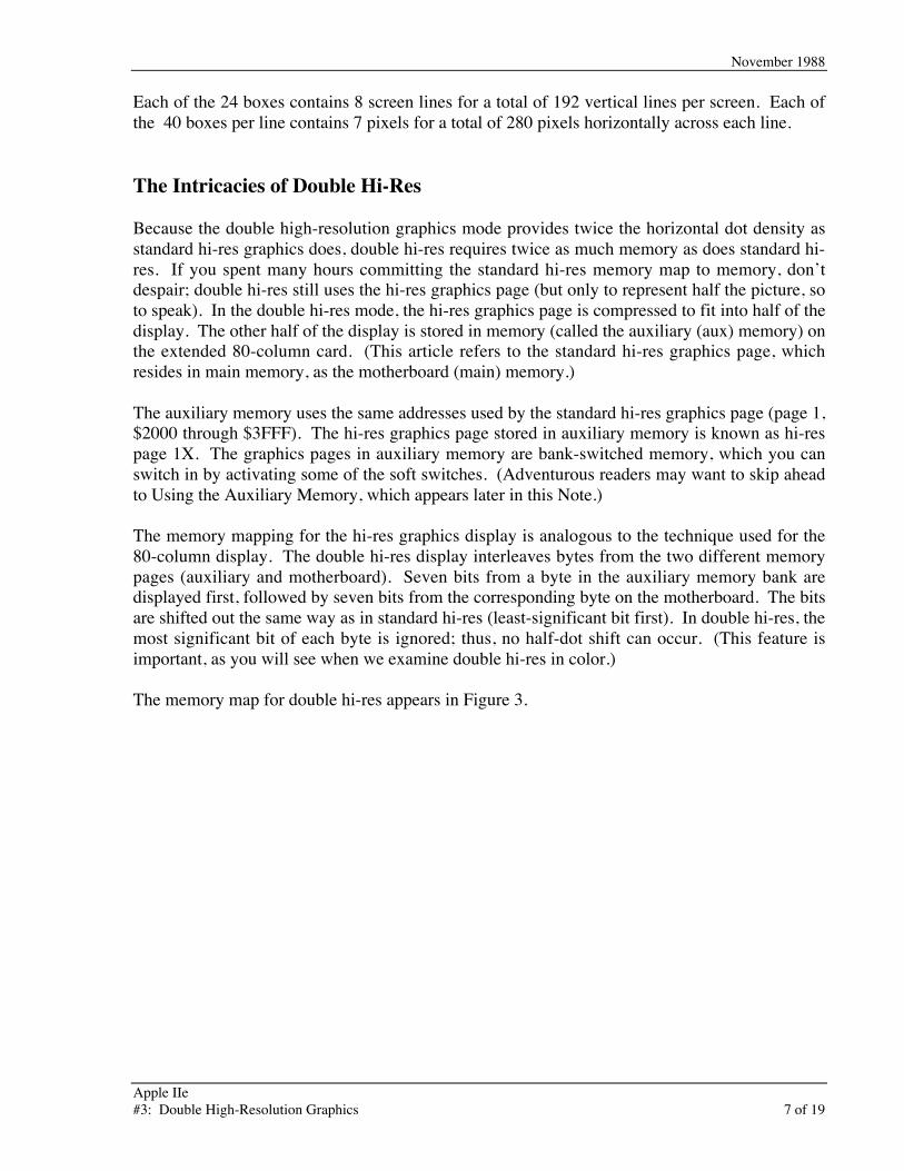
The Figure 1 shows the memory map for the standard hi-res graphics mode.
Apple II Technical Notes
6 of 19 Developer Technical Support
$2000$2080$2100$2180$2200$2280$2300$2380$2028$20A8$2128$21A8$2228$22A8$2328$23A8$2050$20D0$2150$21D0$2250$22D0$2350$23D0
$00 $01 $02 $03 $24 $25 $26 $27
Horizontal Offset
Base
Figure 1–Standard Hi-Res Memory Map
Figure 2 shows the box subdivisions for the memory map in Figure 1.
Offsetfrombase
+$0000+$0400+$0800+$0C00+$1000+$1400+$1800+$1C00
6 5 4 3 2 1 0LSB
Bit
Figure 2–Box Subdivisions of the Standard Memory Map
For example, the first memory address of each screen line for the first few lines is as follows:
$2000, $2400, $2800, $2C00, $3000, $3400, $3800, $3C00, $2080, $2480, etc.
November 1988
Apple IIe#3: Double High-Resolution Graphics 7 of 19
Each of the 24 boxes contains 8 screen lines for a total of 192 vertical lines per screen. Each ofthe 40 boxes per line contains 7 pixels for a total of 280 pixels horizontally across each line.
The Intricacies of Double Hi-Res
Because the double high-resolution graphics mode provides twice the horizontal dot density asstandard hi-res graphics does, double hi-res requires twice as much memory as does standard hi-res. If you spent many hours committing the standard hi-res memory map to memory, don’tdespair; double hi-res still uses the hi-res graphics page (but only to represent half the picture, soto speak). In the double hi-res mode, the hi-res graphics page is compressed to fit into half of thedisplay. The other half of the display is stored in memory (called the auxiliary (aux) memory) onthe extended 80-column card. (This article refers to the standard hi-res graphics page, whichresides in main memory, as the motherboard (main) memory.)
The auxiliary memory uses the same addresses used by the standard hi-res graphics page (page 1,$2000 through $3FFF). The hi-res graphics page stored in auxiliary memory is known as hi-respage 1X. The graphics pages in auxiliary memory are bank-switched memory, which you canswitch in by activating some of the soft switches. (Adventurous readers may want to skip aheadto Using the Auxiliary Memory, which appears later in this Note.)
The memory mapping for the hi-res graphics display is analogous to the technique used for the80-column display. The double hi-res display interleaves bytes from the two different memorypages (auxiliary and motherboard). Seven bits from a byte in the auxiliary memory bank aredisplayed first, followed by seven bits from the corresponding byte on the motherboard. The bitsare shifted out the same way as in standard hi-res (least-significant bit first). In double hi-res, themost significant bit of each byte is ignored; thus, no half-dot shift can occur. (This feature isimportant, as you will see when we examine double hi-res in color.)
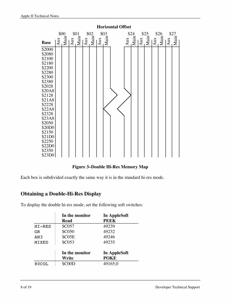
The memory map for double hi-res appears in Figure 3.
Apple II Technical Notes
8 of 19 Developer Technical Support
$2000$2080$2100$2180$2200$2280$2300$2380$2028$20A8$2128$21A8$2228$22A8$2328$23A8$2050$20D0$2150$21D0$2250$22D0$2350$23D0
$00 $01 $02 $03 $24 $25 $26 $27
Horizontal Offset
Base Aux
Main
Aux
Main
Aux
Main
Aux
Main
Aux
Main
Aux
Main
Aux
Main
Aux
Main
Figure 3–Double Hi-Res Memory Map
Each box is subdivided exactly the same way it is in the standard hi-res mode.
Obtaining a Double-Hi-Res Display
To display the double hi-res mode, set the following soft switches:
In the monitor In AppleSoftRead PEEK
HI-RES $C057 49239GR $C050 49232AN3 $C05E 49246MIXED $C053 49235
In the monitor In AppleSoftWrite POKE
80COL $C00D 49165,0
November 1988
Apple IIe#3: Double High-Resolution Graphics 9 of 19
Annunciator 3 (AN3) must be turned off to get into double hi-res mode. You turn it off byreading location 49246 ($C05E). Note that whenever you press Control-Reset, AN3 is turnedon; therefore, each time you press Control-Reset, you must turn AN3 off again.
If you are using MIXED mode, then the bottom four lines on the screen will display text. If youhave not turned on the 80-column card, then every second character in the bottom four lines oftext will be a random character. (The reason is that although the hardware displays 80 columnsof characters, the firmware only updates the 40-column screen, which consists of the charactersin the odd-numbered columns. The characters in even-numbered columns then consist ofrandom characters taken from text page 1X in the auxiliary memory.)
To remove the even characters from the bottom four lines on the screen, type PR#3<CR> fromAppleSoft (type 3^P in the monitor). This procedure clears the memory locations on page 1X.
Using the Auxiliary Memory
The auxiliary memory consists of several different sections, which you can select by using thesoft switches listed below. A pair of memory locations is dedicated to each switch. (Onelocation turns the switch on; the other turns it off.) You activate a switch by writing to theappropriate memory location. The write instruction itself is what activates the switch; therefore,it does not matter what data you write to the memory location. The soft switches are as follows:
In the monitor In AppleSoftWrite POKE
80STORE off $C000 49152,0on $C001 49153,0
RAMRD off $C002 49154,0on $C003 49155,0
RAMWRT off $C004 49156,0on $C005 49157,0
PAGE2 off $C054 49236,0on $C055 49237,0
HIRES off $C056 49238,0on $C057 49239,0
A routine called AUXMOVE ($C311), located in the 80-column firmware, is also very handy, aswe will see below.
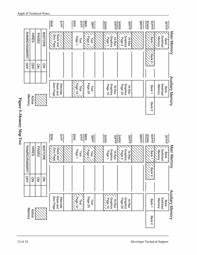
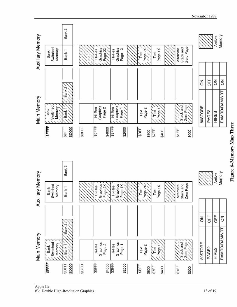
Accessing memory on the auxiliary card with the soft switches has the following characteristics.Memory maps, which help clarify the descriptions, are in Figures 4, 5, and 6.
1. To activate the PAGE2 and HIRES switches, you need only read (PEEK) from thecorresponding memory locations (instead of writing to them, as you do for theother three switches).
Apple II Technical Notes
10 of 19 Developer Technical Support
2. The PAGE2 switch normally selects the display page, in either graphics or textmode, from either page 1 or page 2 of the motherboard memory. However, itdoes so only when the 80STORE switch is off.
3. If the 80STORE switch is on, then the function of the PAGE2 switch changes.When 80STORE is on, then PAGE2 switches in the text page, locations $400-7FF, from auxiliary memory (text page 1X), instead of switching the displayscreen to the alternate video page (page 2 on the motherboard). When 80STOREis on, the PAGE2 switch determines which memory bank (auxiliary ormotherboard) is used during any access to addresses $400 through 7FF. When the80STORE switch is on, it has priority over all other switches.
4. If the 80STORE switch is on, then the PAGE2 switch only switches in thegraphics page 1X from the auxiliary memory if the HIRES switch is also on.(Note that this circumstance is slightly different from that described in item 3.)When 80STORE is on, and if the HIRES switch is also on, then the PAGE2switch selects the memory bank (auxiliary or motherboard) for accesses to amemory location within the range $2000 through 3FFF. If the HIRES switch isoff, then any access to an memory location within the range $2000 through 3FFFuses the motherboard memory, regardless of the state of the PAGE2 switch.
5. If the 80STORE switch is off, and if the RAMRD and RAMWRT switches are on,then any reading from or writing to address space $200-$BFFF gains access to theauxiliary memory. If only one of the switches, RAMRD, for example, is set, thenonly the appropriate operation (in this case a read) will be performed on theauxiliary memory. If only RAMWRT is set, then all write operations access theauxiliary memory. When the 80STORE switch is on, it has higher priority thanthe RAMRD and RAMWRT switches.

November 1988
Apple IIe#3: Double High-Resolution Graphics 11 of 19
$D00
0
$3F
FF
$400
0
$FF
FF
$DF
FF
Ban
k S
witc
hed
Mem
ory
Ban
k 1
Ban
k 2
$BF
FF
$5F
FF
$200
0
$BF
F
$7F
F
$800
$400
$1F
F
$000
Sta
ck a
ndZ
ero
Pag
e
Tex
t P
age
1
Tex
t P
age
2
Hi-R
es
Gra
phic
sP
age
1
Hi-R
es
Gra
phic
sP
age
2
Ban
k S
witc
hed
Mem
ory
Ban
k 1
Ban
k 2
Alte
rnat
eS
tack
and
Zer
o P
age
Tex
t P
age
1X
Tex
t P
age
2X
Hi-R
es
Gra
phic
sP
age
1X
Hi-R
es
Gra
phic
sP
age
2X
Mai
n M
emor
yA
uxili
ary
Mem
ory
80S
TO
RE
PA
GE
2
HIR
ES
RA
MR
D/R
AM
WR
T
OF
FO
N
X X
OF
F
OF
F
X
OF
F
Act
ive
Mem
ory
$D00
0
$3F
FF
$400
0
$FF
FF
$DF
FF
Ban
k S
witc
hed
Mem
ory
Ban
k 1
Ban
k 2
$BF
FF
$5F
FF
$200
0
$BF
F
$7F
F
$800
$400
$1F
F
$000
Sta
ck a
ndZ
ero
Pag
e
Tex
t P
age
1
Tex
t P
age
2
Hi-R
es
Gra
phic
sP
age
1
Hi-R
es
Gra
phic
sP
age
2
Ban
k S
witc
hed
Mem
ory
Ban
k 1
Ban
k 2
Alte
rnat
eS
tack
and
Zer
o P
age
Tex
t P
age
1X
Tex
t P
age
2X
Hi-R
es
Gra
phic
sP
age
1X
Hi-R
es
Gra
phic
sP
age
2X
Mai
n M
emor
yA
uxili
ary
Mem
ory
80S
TO
RE
PA
GE
2
HIR
ES
RA
MR
D/R
AM
WR
T
OF
FO
N
X X ON
ON X ON
Act
ive
Mem
ory
Fig
ure
4–M
emor
y M
ap O
ne
Apple II Technical Notes
12 of 19 Developer Technical Support
$D000
$3FF
F$4000
$FF
FF
$DF
FF
Bank
Sw
itchedM
emory
Bank 1
Bank 2
$BF
FF
$5FF
F
$2000
$BF
F
$7FF
$800
$400
$1FF
$000
Stack and
Zero P
age
Text
Page 1
Text
Page 2
Hi-R
es G
raphicsP
age 1
Hi-R
es G
raphicsP
age 2
Bank
Sw
itchedM
emory
Bank 1
Bank 2
Alternate
Stack and
Zero P
age
Text
Page 1X
Text
Page 2X
Hi-R
es G
raphicsP
age 1X
Hi-R
es G
raphicsP
age 2X
Main M
emory
Auxiliary M
emory
80ST
OR
E
PA
GE
2
HIR
ES
RA
MR
D/R
AM
WR
T
ON
ON
OF
F
OF
F
Active
Mem
ory
$D000
$3FF
F$4000
$FF
FF
$DF
FF
Bank
Sw
itchedM
emory
Bank 1
Bank 2
$BF
FF
$5FF
F
$2000
$BF
F
$7FF
$800
$400
$1FF
$000
Stack and
Zero P
age
Text
Page 1
Text
Page 2
Hi-R
es G
raphicsP
age 1
Hi-R
es G
raphicsP
age 2
Bank
Sw
itchedM
emory
Bank 1
Bank 2
Alternate
Stack and
Zero P
age
Text
Page 1X
Text
Page 2X
Hi-R
es G
raphicsP
age 1X
Hi-R
es G
raphicsP
age 2X
Main M
emory
Auxiliary M
emory
80ST
OR
E
PA
GE
2
HIR
ES
RA
MR
D/R
AM
WR
T
ON
ON
ON
OF
F
Active
Mem
ory
Figure 5–M
emory M
ap Tw
o
November 1988
Apple IIe#3: Double High-Resolution Graphics 13 of 19
$D00
0
$3F
FF
$400
0
$FF
FF
$DF
FF
Ban
k S
witc
hed
Mem
ory
Ban
k 1
Ban
k 2
$BF
FF
$5F
FF
$200
0
$BF
F
$7F
F
$800
$400
$1F
F
$000
Sta
ck a
ndZ
ero
Pag
e
Tex
t P
age
1
Tex
t P
age
2
Hi-R
es
Gra
phic
sP
age
1
Hi-R
es
Gra
phic
sP
age
2
Ban
k S
witc
hed
Mem
ory
Ban
k 1
Ban
k 2
Alte
rnat
eS
tack
and
Zer
o P
age
Tex
t P
age
1X
Tex
t P
age
2X
Hi-R
es
Gra
phic
sP
age
1X
Hi-R
es
Gra
phic
sP
age
2X
Mai
n M
emor
yA
uxili
ary
Mem
ory
80S
TO
RE
PA
GE
2
HIR
ES
RA
MR
D/R
AM
WR
T
ON
OF
F
OF
F
ON
Act
ive
Mem
ory
$D00
0
$3F
FF
$400
0
$FF
FF
$DF
FF
Ban
k S
witc
hed
Mem
ory
Ban
k 1
Ban
k 2
$BF
FF
$5F
FF
$200
0
$BF
F
$7F
F
$800
$400
$1F
F
$000
Sta
ck a
ndZ
ero
Pag
e
Tex
t P
age
1
Tex
t P
age
2
Hi-R
es
Gra
phic
sP
age
1
Hi-R
es
Gra
phic
sP
age
2
Ban
k S
witc
hed
Mem
ory
Ban
k 1
Ban
k 2
Alte
rnat
eS
tack
and
Zer
o P
age
Tex
t P
age
1X
Tex
t P
age
2X
Hi-R
es
Gra
phic
sP
age
1X
Hi-R
es
Gra
phic
sP
age
2X
Mai
n M
emor
yA
uxili
ary
Mem
ory
80S
TO
RE
PA
GE
2
HIR
ES
RA
MR
D/R
AM
WR
T
ON
OF
F
ON
ON
Act
ive
Mem
ory
Fig
ure
6–M
emor
y M
ap T
hree
Apple II Technical Notes
14 of 19 Developer Technical Support
Shortcuts: Writing to Auxiliary Memory from the Keyboard
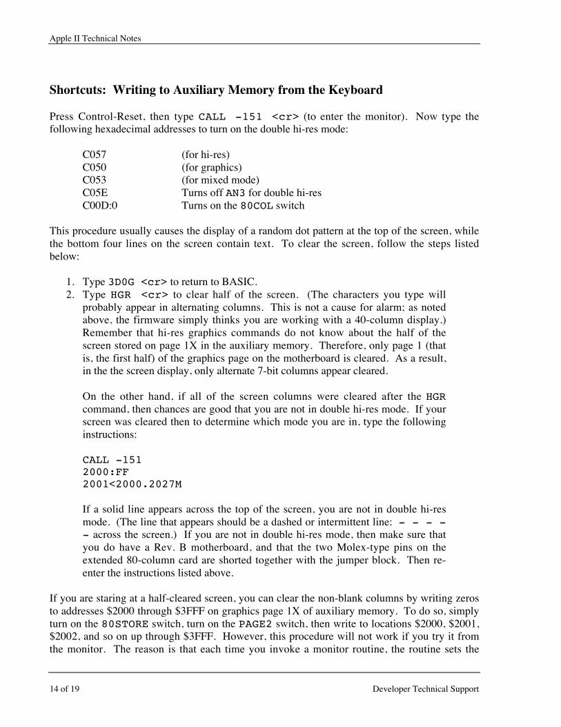
Press Control-Reset, then type CALL -151 <cr> (to enter the monitor). Now type thefollowing hexadecimal addresses to turn on the double hi-res mode:
C057 (for hi-res)C050 (for graphics)C053 (for mixed mode)C05E Turns off AN3 for double hi-resC00D:0 Turns on the 80COL switch
This procedure usually causes the display of a random dot pattern at the top of the screen, whilethe bottom four lines on the screen contain text. To clear the screen, follow the steps listedbelow:
1. Type 3D0G <cr> to return to BASIC.2. Type HGR <cr> to clear half of the screen. (The characters you type will
probably appear in alternating columns. This is not a cause for alarm; as notedabove, the firmware simply thinks you are working with a 40-column display.)Remember that hi-res graphics commands do not know about the half of thescreen stored on page 1X in the auxiliary memory. Therefore, only page 1 (thatis, the first half) of the graphics page on the motherboard is cleared. As a result,in the the screen display, only alternate 7-bit columns appear cleared.
On the other hand, if all of the screen columns were cleared after the HGRcommand, then chances are good that you are not in double hi-res mode. If yourscreen was cleared then to determine which mode you are in, type the followinginstructions:
CALL -1512000:FF2001<2000.2027M
If a solid line appears across the top of the screen, you are not in double hi-resmode. (The line that appears should be a dashed or intermittent line: - - - -- across the screen.) If you are not in double hi-res mode, then make sure thatyou do have a Rev. B motherboard, and that the two Molex-type pins on theextended 80-column card are shorted together with the jumper block. Then re-enter the instructions listed above.
If you are staring at a half-cleared screen, you can clear the non-blank columns by writing zerosto addresses $2000 through $3FFF on graphics page 1X of auxiliary memory. To do so, simplyturn on the 80STORE switch, turn on the PAGE2 switch, then write to locations $2000, $2001,$2002, and so on up through $3FFF. However, this procedure will not work if you try it fromthe monitor. The reason is that each time you invoke a monitor routine, the routine sets the
November 1988
Apple IIe#3: Double High-Resolution Graphics 15 of 19
PAGE2 switch back to page 1 so that it can display the most recent command that you entered.When you try to write to $2000, etc. on the auxiliary card, instead it will write to themotherboard memory.
Another way to obtain the desired result is to use the monitor’s USER command, which forces ajump to memory location $3F8. You can place a JMP instruction starting at this memorylocation, so the program will jump to a routine that writes into hi-res page 1X. Fortunately, thesystem already contains such a routine: AUXMOVE.
Using AUXMOVE
You use the AUXMOVE routine to move data blocks between main and auxiliary memory, but thetask still remains of setting up the routine so that it knows which data to write, and where towrite it. To use this routine, some byte pairs in the zero page must be setup with the data blockaddresses, and the carry bit must be fixed to indicate the direction of the move. You may not besurprised to learn that the byte pairs in the zero page used by AUXMOVE are also the scratch-padregisters used by the monitor during instruction execution. The result is that while you type theaddresses for the monitor’s move command, those addresses are being stored in the byte pairsused by AUXMOVE. Thereafter, you can call the AUXMOVE command directly, using the USER(Control-Y) command.
In practice, then, enter the following instructions:
C00A:0 (turns on the 80-column ROM, which contains theAUXMOVE routine)
C000:0 (reason explained below)3F8: 4C 11 C3 (the jump to AUXMOVE)2000<2000.3FFF ^Y (where ^Y indicates that you should type Control-
Y)
The syntax for this USER (Control-Y) command is:
{AUXdest}<{MBstart}.{MBend}^Y
The command copies the values in the range MBstart to MBend in the motherboard memoryinto the auxiliary memory beginning at AUXdest. This command is analogous to the MOVEcommand.
You can use this procedure to transfer any block of data from the motherboard memory to hi-respage 1X. Working directly from the keyboard, you can use a data block transferred this way tofill in any part of a double hi-res screen image. The image to be stored in hi-res page 1X (i.e.,the image that will be displayed in the even-numbered columns of the double hi-res picture) mustfirst be stored in the motherboard memory. You can then use the Control-Y command to transferthe image to hi-res page 1X.
Apple II Technical Notes
16 of 19 Developer Technical Support
The AUXMOVE routine uses the RAMRD and RAMWRT switches to transfer the data blocks.Because the 80STORE switch overrides the RAMRD and RAMWRT switches, the 80STOREswitch must be turned off—otherwise it would keep the transfer from occurring properly (hencethe write to $C000 above).
If the 80STORE and HIRES switches are on and PAGE2 is off, when you execute AUXMOVE,any access to an address located within the range from $2000 to $3FFF inclusive would use themotherboard memory, regardless of how RAMRD and RAMWRT are set. Entering the commandC000:0 <cr> turns off 80STORE, thus letting the RAMRD and RAMWRT switches control thememory banking.
The Control-Y trick described above only works for transferring data blocks from the main(motherboard) memory to auxiliary memory (because the monitor always enters the AUXMOVEroutine with the carry bit set). To move data blocks from the auxiliary memory to the mainmemory, you must enter AUXMOVE with the carry bit clear. You can use the following routine totransfer data blocks in either direction:
301:AD 0 3 (loads the contents of address $300 into the accumulator)304:2A (rotates the most-significant bit into the carry flag)305:4C 11 C3 (jump to $C311 (AUXMOVE))3F8:4C 1 3 (sets the Control-Y command to jump to address $301)
Before using this routine, you must modify memory location $300, depending on the direction inwhich you want to transfer the data blocks. If the transfer is from the auxiliary memory to themotherboard, you must clear location $300 to zero. If the transfer is from the motherboard to theauxiliary memory, you must set location $300 to $FF.
Two Double Hi-Res Pages
So far, we have only discussed using graphics pages 1 and 1X to display double hi-res pictures.But—analogous to the standard hi-res pages 1 and 2—two double hi-res pages exist: pages 1and 1X, at locations $2000 through 3FFF, and pages 2 and 2X, at locations $4000 through 5FFF.The only trick in displaying the second double hi-res page is that you must turn off the80STORE switch. If the 80STORE switch is on, then only the first page (1 and 1X) is displayed.Go ahead and try it:
C000:0 to turn off the 80STORE switchC055 to turn on the PAGE2 switch
The screen will fill with another display of random bits. Clear the screen using the instructionslisted above (in the Using AUXMOVE section ). However, this time, use addresses $4000 through5FFF instead. (Don’t be alarmed by the fact that the figures you are typing are not displayed onthe screen. They are being “displayed” on text page 1.)
4000:04001<4000.5FFFM
November 1988
Apple IIe#3: Double High-Resolution Graphics 17 of 19
4000<4000.5FFF ^Y
You will be delighted to learn that you can also use this trick to display two 80-column textscreens. The only problem here is that the 80-column firmware continually turns on the80STORE switch, which prevents the display of the second 80-column screen. However, if youwrite your own 80-column display driver, then you can use both of the 80-column screens.
Color Madness
It should come as no surprise that color-display techniques in double hires are different fromcolor-display techniques in standard hi-res. This difference is because the half-dot shift does notexist in double hi-res mode.
Instead of going into a dissertation on how a television set decodes and displays a color signal,I’ll simply explain how to generate color in double hi-res mode. In the following examples, theterm color monitor refers to either an NTSC monitor or a color television set. Both work;however, the displays will be much harder to see on the color television. The generation of colorin double hi-res demands sacrifices. A 560 x 192 dot display is not possible in color. Instead,the horizontal resolution decreases by a factor of four (140 dots across the screen). Just as with ablack-and-white monitor, a simple correspondence exists between memory and the pixels on thescreen. The difference is that four bits are required to determine each color pixel. These fourbits represent 16 different combinations: one for each of the colors available in double hi-res.(These are the same colors that are available in the low-resolution mode.)
Let’s start by exploring the pattern that must be stored in memory to draw a single colored lineacross the screen. Use a color demonstration program (such as COLOR.TEST from older DOS3.3 System Master disks) to adjust the colors displayed by your monitor. After you haveadjusted the colors, exit from the color demonstration program.
The instructions that appear below are divided into groups separated by blank lines. Because itis very difficult (and, on a television set, almost impossible) to read the characters you are typingas they appear on the screen, you will probably make typing errors. If the instructions appear notto work, then start again from the beginning of a group of instructions.
CALL -151 (to get into the monitor routine/program)C050 (This set of instructions puts the computerCO57 into double hi-res model.C05EC00D:02000:0 (This set of instructions clears first one half2001<2000.3FFFM of the screen, and then the other half of3F8: 4C 11 C3 the screen.)2000<2000.3FFF^Y
2100:11 4 (Two red dots appear on top left of screen)2102<2100.2126M (A dashed red line appears across screen)
Apple II Technical Notes
18 of 19 Developer Technical Support
2150:8 22 (Two green dots appear near bottom left)2152<2150.2175M (Dashed green line appears across screen)
2100<2150.2177^Y (Fills in the red line)
In contrast to conditions in standard hi-res, no half-dot shift occurs, and the most-significant bitof each byte is not used.
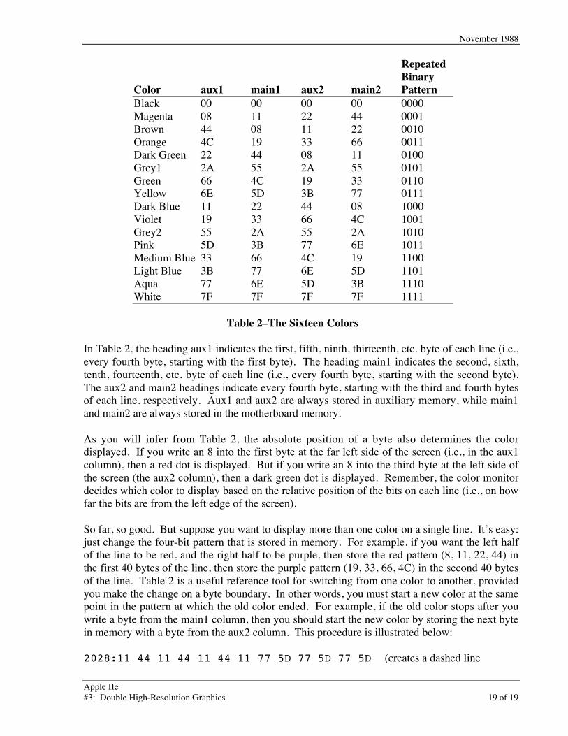
As noted above, four bits determine a color. You can paint a one-color line across the screensimply by repeating a four-bit pattern across the screen, but it is much easier to write a wholebyte rather than just change four bits at a time. Since only seven bits of each byte are displayed(as noted earlier in our discussion of black-and-white double hi-res) and the pattern is four bitswide, it repeats itself every 28 bits or four bytes. Use the instructions listed below to draw a lineof any color across the screen by repeating a four byte pattern for the color as shown in Table 2.
2200: main1 main2 (Colored dots appear at the left edge)2202<2200.2226M (A dashed, colored line appears)
2250: aux1 aux22250<2250.2276M
2200<2250.2276^Y (Fills in line, using the selected color)
November 1988
Apple IIe#3: Double High-Resolution Graphics 19 of 19
RepeatedBinary
Color aux1 main1 aux2 main2 PatternBlack 00 00 00 00 0000Magenta 08 11 22 44 0001Brown 44 08 11 22 0010Orange 4C 19 33 66 0011Dark Green 22 44 08 11 0100Grey1 2A 55 2A 55 0101Green 66 4C 19 33 0110Yellow 6E 5D 3B 77 0111Dark Blue 11 22 44 08 1000Violet 19 33 66 4C 1001Grey2 55 2A 55 2A 1010Pink 5D 3B 77 6E 1011Medium Blue 33 66 4C 19 1100Light Blue 3B 77 6E 5D 1101Aqua 77 6E 5D 3B 1110White 7F 7F 7F 7F 1111
Table 2–The Sixteen Colors
In Table 2, the heading aux1 indicates the first, fifth, ninth, thirteenth, etc. byte of each line (i.e.,every fourth byte, starting with the first byte). The heading main1 indicates the second, sixth,tenth, fourteenth, etc. byte of each line (i.e., every fourth byte, starting with the second byte).The aux2 and main2 headings indicate every fourth byte, starting with the third and fourth bytesof each line, respectively. Aux1 and aux2 are always stored in auxiliary memory, while main1and main2 are always stored in the motherboard memory.
As you will infer from Table 2, the absolute position of a byte also determines the colordisplayed. If you write an 8 into the first byte at the far left side of the screen (i.e., in the aux1column), then a red dot is displayed. But if you write an 8 into the third byte at the left side ofthe screen (the aux2 column), then a dark green dot is displayed. Remember, the color monitordecides which color to display based on the relative position of the bits on each line (i.e., on howfar the bits are from the left edge of the screen).
So far, so good. But suppose you want to display more than one color on a single line. It’s easy:just change the four-bit pattern that is stored in memory. For example, if you want the left halfof the line to be red, and the right half to be purple, then store the red pattern (8, 11, 22, 44) inthe first 40 bytes of the line, then store the purple pattern (19, 33, 66, 4C) in the second 40 bytesof the line. Table 2 is a useful reference tool for switching from one color to another, providedyou make the change on a byte boundary. In other words, you must start a new color at the samepoint in the pattern at which the old color ended. For example, if the old color stops after youwrite a byte from the main1 column, then you should start the new color by storing the next bytein memory with a byte from the aux2 column. This procedure is illustrated below:
2028:11 44 11 44 11 44 11 77 5D 77 5D 77 5D (creates a dashed line
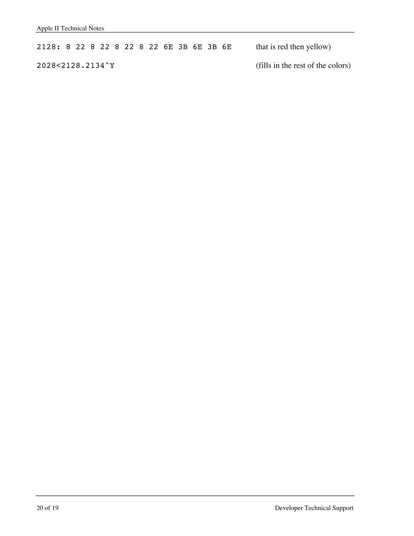
Apple II Technical Notes
20 of 19 Developer Technical Support
2128: 8 22 8 22 8 22 8 22 6E 3B 6E 3B 6E that is red then yellow)
2028<2128.2134^Y (fills in the rest of the colors)
November 1988
Apple IIe#3: Double High-Resolution Graphics 21 of 19
Switching Colors in Mid-Byte
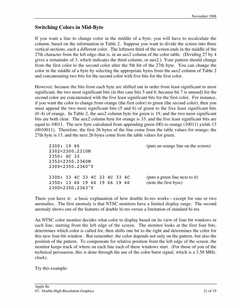
If you want a line to change color in the middle of a byte, you will have to recalculate thecolumn, based on the information in Table 2. Suppose you want to divide the screen into threevertical sections, each a different color. The leftmost third of the screen ends in the middle of the27th character from the left edge–that is, in an aux2 column of the color table. (Dividing 27 by 4gives a remainder of 3, which indicates the third column, or aux2.) Your pattern should changefrom the first color to the second color after the 5th bit of the 27th byte. You can change thecolor in the middle of a byte by selecting the appropriate bytes from the aux2 column of Table 2and concatenating two bits for the second color with five bits for the first color.
However, because the bits from each byte are shifted out in order from least significant to mostsignificant, the two most significant bits (in this case bits 5 and 6, because bit 7 is unused) for thesecond color are concatenated with the five least significant bits for the first color. For instance,if you want the color to change from orange (the first color) to green (the second color), then youmust append the two most significant bits (5 and 6) of green to the five least significant bits(0–4) of orange. In Table 2, the aux2 column byte for green is 19, and the two most significantbits are both clear. The aux2 column byte for orange is 33, and the five least significant bits areequal to 10011. The new byte calculated from appending green (00) to orange (10011) yields 13(0010011). Therefore, the first 26 bytes of the line come from the table values for orange; the27th byte is 13, and the next 26 bytes come from the table values for green.
2300: 19 66 (puts an orange line on the screen)2302<2300.2310M2350: 4C 332352<2350.2360M2300<2350.2360^Y
230D: 33 4C 33 4C 33 4C 33 4C (puts a green line next to it)235D: 13 66 19 66 19 66 19 66 (note the first byte)230D<235D.2363^Y
There you have it: a basic explanation of how double hi-res works—except for one or twoanomalies. The first anomaly is that NTSC monitors have a limited display range. The secondanomaly shows one of the features of double hi-res versus a limitation of standard hi-res.
An NTSC color monitor decides what color to display based on its view of four bit windows ineach line, starting from the left edge of the screen. The monitor looks at the first four bits,determines which color is called for, then shifts one bit to the right and determines the color forthis new four-bit window. But remember, the color depends not only on the pattern, but also theposition of the pattern. To compensate for relative position from the left edge of the screen, themonitor keeps track of where on each line each of these windows start. (For those of you of thetechnical persuasion, this is done through the use of the color burst signal, which is a 3.58 MHz.clock).
Try this example:
Apple II Technical Notes
22 of 19 Developer Technical Support
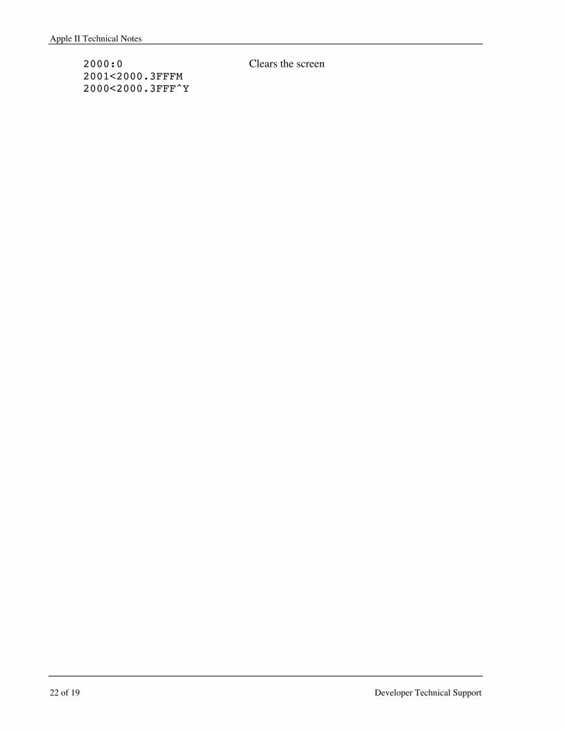
2000:0 Clears the screen2001<2000.3FFFM2000<2000.3FFF^Y
November 1988
Apple IIe#3: Double High-Resolution Graphics 23 of 19
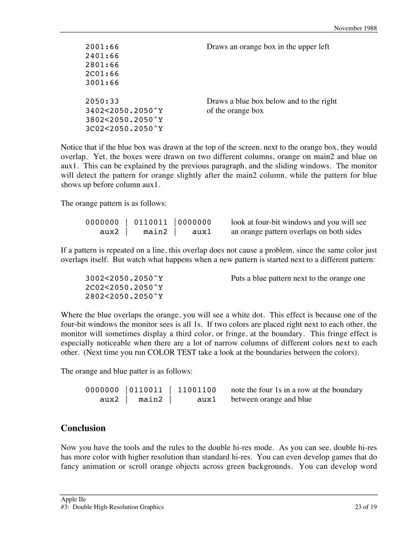
2001:66 Draws an orange box in the upper left2401:662801:662C01:663001:66
2050:33 Draws a blue box below and to the right3402<2050.2050^Y of the orange box3802<2050.2050^Y3C02<2050.2050^Y
Notice that if the blue box was drawn at the top of the screen, next to the orange box, they wouldoverlap. Yet, the boxes were drawn on two different columns, orange on main2 and blue onaux1. This can be explained by the previous paragraph, and the sliding windows. The monitorwill detect the pattern for orange slightly after the main2 column, while the pattern for blueshows up before column aux1.
The orange pattern is as follows:
0000000 | 0110011 |0000000 look at four-bit windows and you will see aux2 | main2 | aux1 an orange pattern overlaps on both sides
If a pattern is repeated on a line, this overlap does not cause a problem, since the same color justoverlaps itself. But watch what happens when a new pattern is started next to a different pattern:
3002<2050.2050^Y Puts a blue pattern next to the orange one2C02<2050.2050^Y2802<2050.2050^Y
Where the blue overlaps the orange, you will see a white dot. This effect is because one of thefour-bit windows the monitor sees is all 1s. If two colors are placed right next to each other, themonitor will sometimes display a third color, or fringe, at the boundary. This fringe effect isespecially noticeable when there are a lot of narrow columns of different colors next to eachother. (Next time you run COLOR TEST take a look at the boundaries between the colors).
The orange and blue patter is as follows:
0000000 |0110011 | 11001100 note the four 1s in a row at the boundary aux2 | main2 | aux1 between orange and blue
Conclusion
Now you have the tools and the rules to the double hi-res mode. As you can see, double hi-reshas more color with higher resolution than standard hi-res. You can even develop games that dofancy animation or scroll orange objects across green backgrounds. You can develop word
Apple II Technical Notes
24 of 19 Developer Technical Support
processing programs which use different fonts or proportional character sets in black and white.Have fun playing with his new mode.
Further Reference• Apple IIe Technical Reference Manual• Apple IIc Technical Reference Manual, Second Edition• Apple IIGS Hardware Reference
Apple IIe#4: RDY Line 1 of 6
Apple IITechnical Notes
Developer Technical SupportApple IIe#4: RDY Line
Revised by: Glenn A. Baxter November 1988Written by: Peter Baum July 1984
This Technical Note describes an input signal to the 6502 microprocessor called the RDY line.
Using the RDY Line on the Apple IIe and Apple ][+
Though the 6502 was one of the first commercially successful microprocessors sold, thedesigners had foresight to include some very useful functions. Because many early peripheralsproducts were very slow devices, a microprocessor could not read from the device directly. Toconnect these slow devices onto the Apple peripheral bus so the 6502 can read data from themrequires either buffering the device or slowing down the processor. Though most people wouldtry to buffer the device, sometimes it is not feasible. When buffering is not possible, a peripheraldevice can pull the RDY line to slow down the processor long enough to read a byte. Thistechnique can be used by slow devices to communicate with the 6502.
The RDY line allows a peripheral card to halt the microprocessor during read operations(opcode, operand, or data fetches—reads ) with the output address lines reflecting the currentaddress being fetched. If a peripheral device cannot get data on the bus fast enough to meet thesetup time of the 6502, then the peripheral card can pull the RDY line low and tell the 6502 towait. This cannot be done during a 6502 write cycle because the 6502 does not wait duringwrites.
For the 6502 to read a valid data byte from a peripheral card, the card has about 800 ns from thetime the addresses are valid to put the data on the bus. The data must be setup on the bus withinapproximately 400 ns from the time that the I/O STROBE, I/O SELECT, or DEVICE SELECTsignal on the peripheral slot goes true. If a device pulls the RDY line low for one clock cycle,the device will have approximately 1.4 µs, instead of the 400 ns, to put out valid data. The RDYline can be pulled low for more than one cycle—in fact, there is no limit. A device that takes100 µs to send data can just hold the RDY line low for 100 cycles. Hence, this technique willallow any slower device to get on the bus and send data to the 6502.
This is a bit different than DMA on the Apple IIs. DMA actually prevents the CPU fromreceiving a clock signal, whereas the RDY line is actually a function of the processor. In AppleII DMA, the 6502 CPU will die after approximately 15 clocks because it depends on the clock torefresh its internal registers. (The 6502 is dynamic, whereas the 65C02 is static, and therefore
Apple II Technical Notes
2 of 6 Developer Technical Support
not affected by the absence of clock information). In the case of the RDY line, the CPU isinternally told to just not complete its bus cycle until RDY is de-asserted. This is a similarconcept to DTACK on the Motorola 68000 series CPUs.
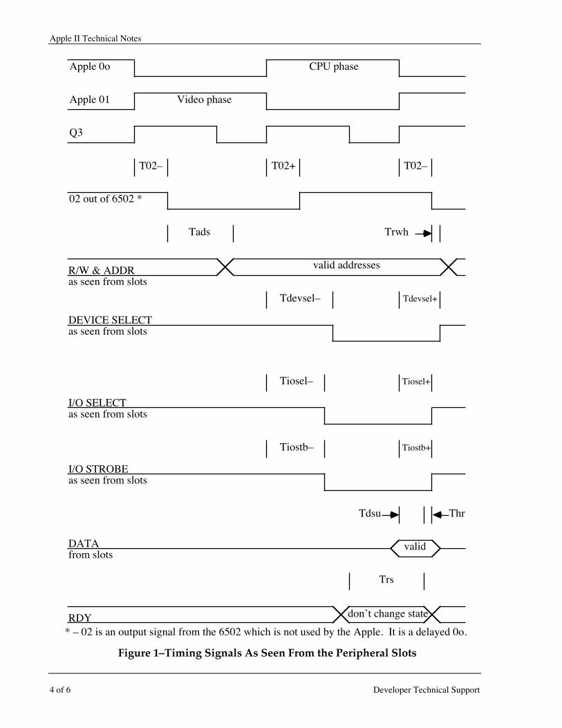
The RDY line is typically pulled low during PH1, but the specification sheets for the 6502 showthat it can be pulled anytime before the last 200 ns of PH2. The PH2 line is not used by theApple II and is an unused output from the 6502. It is basically the same as the PH0 line with alittle delay. Before I explain when to use (or not use, in some cases) the RDY line, let us firstlook at some timing diagrams of the Apple system.
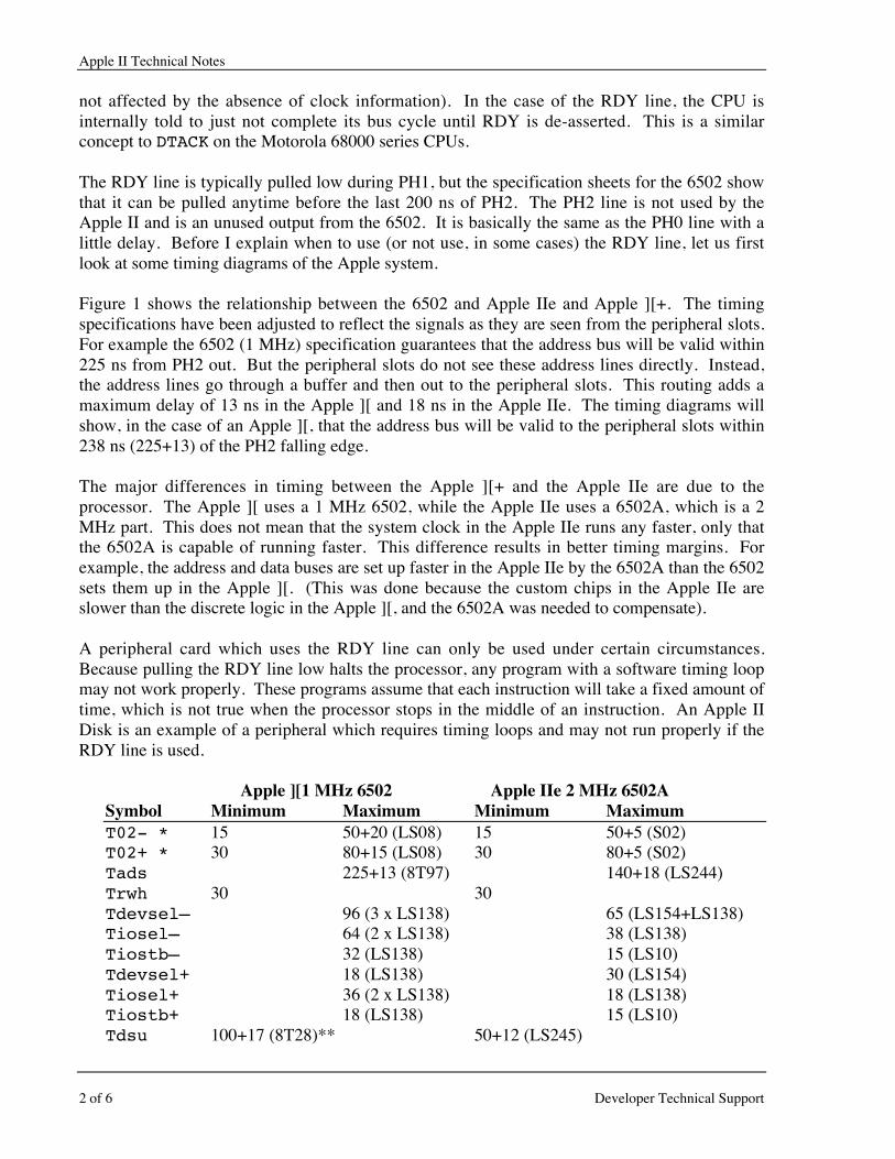
Figure 1 shows the relationship between the 6502 and Apple IIe and Apple ][+. The timingspecifications have been adjusted to reflect the signals as they are seen from the peripheral slots.For example the 6502 (1 MHz) specification guarantees that the address bus will be valid within225 ns from PH2 out. But the peripheral slots do not see these address lines directly. Instead,the address lines go through a buffer and then out to the peripheral slots. This routing adds amaximum delay of 13 ns in the Apple ][ and 18 ns in the Apple IIe. The timing diagrams willshow, in the case of an Apple ][, that the address bus will be valid to the peripheral slots within238 ns (225+13) of the PH2 falling edge.
The major differences in timing between the Apple ][+ and the Apple IIe are due to theprocessor. The Apple ][ uses a 1 MHz 6502, while the Apple IIe uses a 6502A, which is a 2MHz part. This does not mean that the system clock in the Apple IIe runs any faster, only thatthe 6502A is capable of running faster. This difference results in better timing margins. Forexample, the address and data buses are set up faster in the Apple IIe by the 6502A than the 6502sets them up in the Apple ][. (This was done because the custom chips in the Apple IIe areslower than the discrete logic in the Apple ][, and the 6502A was needed to compensate).
A peripheral card which uses the RDY line can only be used under certain circumstances.Because pulling the RDY line low halts the processor, any program with a software timing loopmay not work properly. These programs assume that each instruction will take a fixed amount oftime, which is not true when the processor stops in the middle of an instruction. An Apple IIDisk is an example of a peripheral which requires timing loops and may not run properly if theRDY line is used.
Apple ][1 MHz 6502 Apple IIe 2 MHz 6502ASymbol Minimum Maximum Minimum MaximumT02- * 15 50+20 (LS08) 15 50+5 (S02)T02+ * 30 80+15 (LS08) 30 80+5 (S02)Tads 225+13 (8T97) 140+18 (LS244)Trwh 30 30Tdevsel– 96 (3 x LS138) 65 (LS154+LS138)Tiosel– 64 (2 x LS138) 38 (LS138)Tiostb– 32 (LS138) 15 (LS10)Tdevsel+ 18 (LS138) 30 (LS154)Tiosel+ 36 (2 x LS138) 18 (LS138)Tiostb+ 18 (LS138) 15 (LS10)Tdsu 100+17 (8T28)** 50+12 (LS245)

November 1988
Apple IIe#4: RDY Line 3 of 6
Thr 10 10Trs *** 200 200
(All times are given in nanoseconds (ns).)* load = 100 pf.** The RFI versions of the Apple ][+, revisions A through D motherboards, use an 8304
instead an 8T28.*** The RDY line must never change states within Trs to end of 02.
Table 1–Timing Specifications for Figure 1
Apple II Technical Notes
4 of 6 Developer Technical Support
R/W & ADDRas seen from slots
* – 02 is an output signal from the 6502 which is not used by the Apple. It is a delayed 0o.
Apple 0o
Apple 01
Q3
02 out of 6502 *
CPU phase
Video phase
T02– T02+ T02–
Tads Trwh
valid addresses
DEVICE SELECTas seen from slots
Tdevsel– Tdevsel+
I/O SELECTas seen from slots
I/O STROBEas seen from slots
Tiosel–
Tiostb–
Tiosel+
Tiostb+
DATAfrom slots
valid
Tdsu Thr
Trs
don’t change stateRDY
Figure 1–Timing Signals As Seen From the Peripheral Slots
November 1988
Apple IIe#4: RDY Line 5 of 6
Table 1 lists three different type of numbers. If a number is by itself, then it is just thecorresponding 6502 or 6502A specification. If a number is followed by parenthesis, then itrepresents the delay, produced by TTL gates, between the 6502 and the peripheral slots. Thecharacters in the parenthesis denote the part number(s) of the part(s) which generated the delay.These parts are typically 74’ series TTL except for the 8T28 and 8T97. If there are two numbersin a column with a plus sign (+) then the first number signifies the 6502 specification and thesecond the TTL delay, with the corresponding part number. Most of the TTL delay times arefrom the Texas Instrument data books. The 6502 specifications are from the Synertek 6502 datasheet and from Synertek application note AN2 - SY6500.
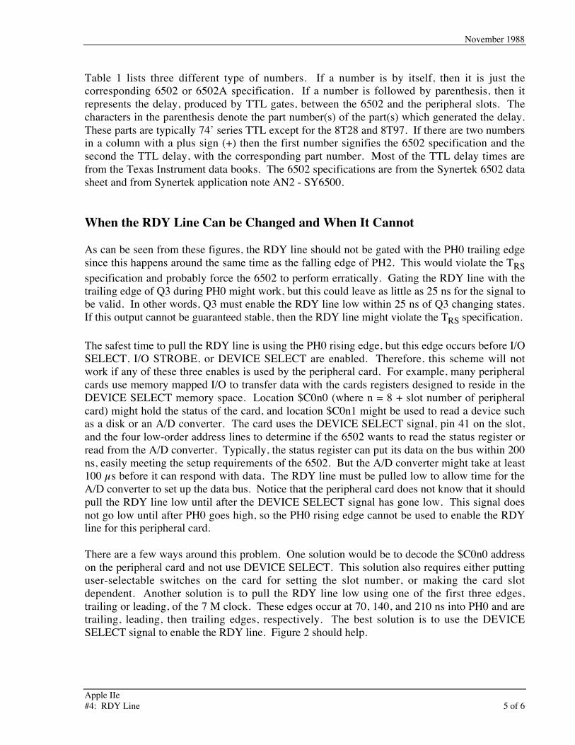
When the RDY Line Can be Changed and When It Cannot
As can be seen from these figures, the RDY line should not be gated with the PH0 trailing edgesince this happens around the same time as the falling edge of PH2. This would violate the TRSspecification and probably force the 6502 to perform erratically. Gating the RDY line with thetrailing edge of Q3 during PH0 might work, but this could leave as little as 25 ns for the signal tobe valid. In other words, Q3 must enable the RDY line low within 25 ns of Q3 changing states.If this output cannot be guaranteed stable, then the RDY line might violate the TRS specification.
The safest time to pull the RDY line is using the PH0 rising edge, but this edge occurs before I/OSELECT, I/O STROBE, or DEVICE SELECT are enabled. Therefore, this scheme will notwork if any of these three enables is used by the peripheral card. For example, many peripheralcards use memory mapped I/O to transfer data with the cards registers designed to reside in theDEVICE SELECT memory space. Location $C0n0 (where n = 8 + slot number of peripheralcard) might hold the status of the card, and location $C0n1 might be used to read a device suchas a disk or an A/D converter. The card uses the DEVICE SELECT signal, pin 41 on the slot,and the four low-order address lines to determine if the 6502 wants to read the status register orread from the A/D converter. Typically, the status register can put its data on the bus within 200ns, easily meeting the setup requirements of the 6502. But the A/D converter might take at least100 µs before it can respond with data. The RDY line must be pulled low to allow time for theA/D converter to set up the data bus. Notice that the peripheral card does not know that it shouldpull the RDY line low until after the DEVICE SELECT signal has gone low. This signal doesnot go low until after PH0 goes high, so the PH0 rising edge cannot be used to enable the RDYline for this peripheral card.
There are a few ways around this problem. One solution would be to decode the $C0n0 addresson the peripheral card and not use DEVICE SELECT. This solution also requires either puttinguser-selectable switches on the card for setting the slot number, or making the card slotdependent. Another solution is to pull the RDY line low using one of the first three edges,trailing or leading, of the 7 M clock. These edges occur at 70, 140, and 210 ns into PH0 and aretrailing, leading, then trailing edges, respectively. The best solution is to use the DEVICESELECT signal to enable the RDY line. Figure 2 should help.
Apple II Technical Notes
6 of 6 Developer Technical Support
7 M
0o
Q3
DEVICESELECT
validADDRESSR/W*
write cycledon’t pull RDY
6502 halts with addresses &R/W* line valid here
RDY
Do NOT change RDY line at these times.
Figure 2–Timing Diagram
Do Not Pull RDY During Write Cycles
Because there is no acknowledge response from the 6502, the peripheral card must do some ofits own housekeeping and check if a write cycle is taking place. On write cycles, the 6502 willnot halt, but continue running until the next read cycle. After a slow peripheral pulls the RDYline and before it tries to get on the bus, it must make sure the 6502 is not in the middle of a writecycle. Otherwise there will be a bus crash, as both the peripheral card and 6502 try to drive thebus. One simple way to prevent this bus crash from occurring is to make sure the peripheral carddoes not pull the RDY line low during a write cycle. You can guarantee this will not happen bychecking the R/W line when PH0 goes high or DEVICE SELECT goes low. The R/W line isguaranteed to be stable by this time.
November 1988
Apple IIe#4: RDY Line 7 of 6
Releasing the RDY Line
When the RDY line is released, the 6502 will continue the cycle that was originally halted andallow the 6502 to read the data bus. Data will be read on the next trailing edge of PH2 by the6502, as long as RDY does not change within TRS of the end of PH2. When the peripheraldevice has set the data bus up with the correct data, it can release the RDY line to complete theread cycle. Releasing the RDY line has exactly the same constraints as pulling the line; do notchange RDY within 200 ns of the end of PH2.
The RDY line can be released before data has been set up, if the data will be valid withinspecification. This means that RDY can be released in the middle of PH1 if the data bus will bevalid 117 ns before PH2 trailing edge, for the Apple ][ (62 ns for the Apple IIe).
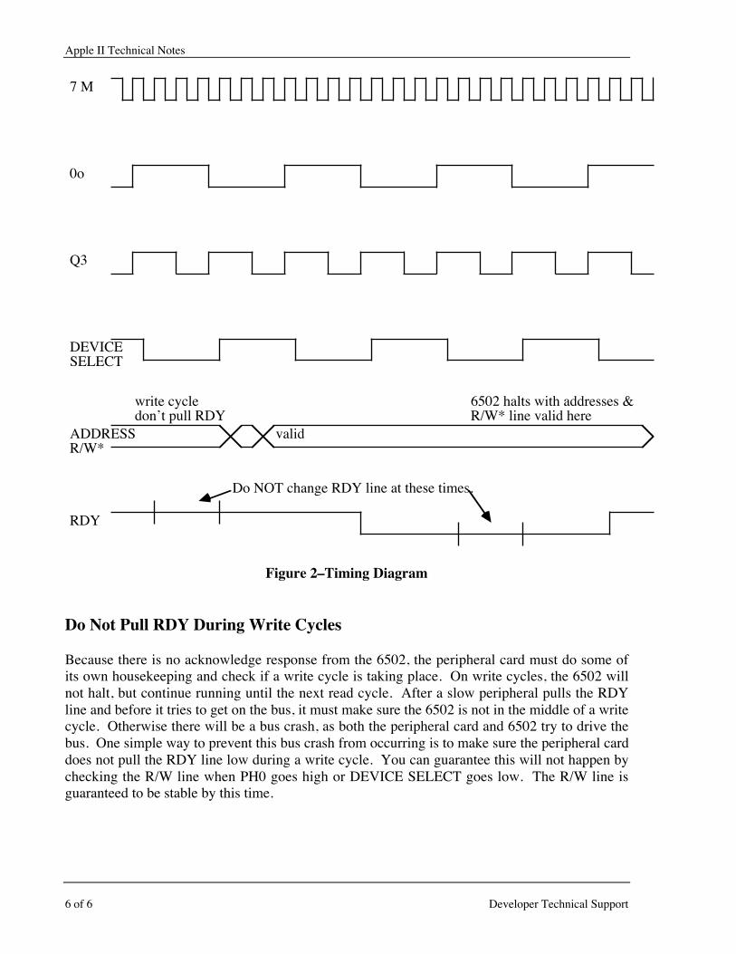
Slow Writes
Since the 6502 cannot be halted during write cycles, if a device requires longer than one cycle toreceive data then the data must be buffered. Here is an example of how to accomplish this:
74LS374
Data bus to slow peripheral
INXFER
DEVICE SELECTorI/O SELECTorI/O STROBE
Figure 3–Buffering Data
Note: It is very easy to overrun the slow peripheral using this scheme, since it onlybuffers one byte at a time. Do not send data twice to the buffer within themaximum allowed time between slow peripheral reads.
Further Reference• Apple IIe Technical Reference Manual
Apple IIe#5: /INH Line 1 of 5
Apple IITechnical Notes
Developer Technical SupportApple IIe#5: /INH Line
Revised by: Glenn A. Baxter November 1988Written by: Peter Baum May 1984
This Technical Note describes how a peripheral card on the Apple IIe should use the inhibit(/INH) line. This information is true for the Apple IIe only.
Using the /INH Line on the Apple IIe
Overview
One of the new features of the Apple IIe is the ability to add more memory or override existingmemory from a peripheral card. This feature, which uses the /INH line on the peripheral slots,has been expanded from its original purpose on the Apple ][+ of disabling the on-board ROMand allowing the language card (RAM) to reside in the same address space. The Apple IIeallows any part of memory to be replaced by memory on a peripheral card. This Note explainshow a peripheral card should use the /INH line.
Uses
Presently, only a few peripheral devices use the /INH line in the IIe for memory expansion. Onetype of card uses /INH for RAM expansion by switching in extra language cards, while anotherclass of cards uses it to extend the built-in 80-column ROM code by replacing it with their ownROM code. Other cards use /INH so that they can have more than one stack and zero page.Future peripheral cards can take advantage of the /INH line to do even fancier memoryexpansion, such as keeping multiple programs running in memory at the same time.
More memory, either ROM or RAM, can be added by mapping the memory into the sameaddress space as existing memory. The processor can then select which memory, the on-boardor the additional, it wants to use by setting a register (or soft switch). This technique ofswitching different blocks of memory into the same address space is called bank switching. Anexample of this technique for extending memory is found in the Apple ][+ language card and inthe bank switched memory on the IIe.
How It Works
Apple II Technical Notes
2 of 5 Developer Technical Support
When the /INH line, pin 32 in slots 1-7, is pulled low, all memory on the motherboard and in theauxiliary slot is disabled (including memory on the 80-column and extended 80-column cards).This action allows a peripheral card in slots 1-7 to enable its memory onto the bus.
When the 6502 reads a byte from memory, the data typically comes from one of three places:motherboard ROM, motherboard RAM, or RAM on one of the 80-column cards in the auxiliaryslot. When the /INH line is pulled low, all of the above mentioned ROM and RAM is disabledand will not drive the data bus. This disabling allows the peripheral slots to drive the bus byenabling data onto it. The 6502 will then read data from the peripheral card instead of a locationon the motherboard or auxiliary slot.
During a 6502 write cycle, if the /INH line is pulled low, then motherboard and auxiliary cardRAM are both disabled. A peripheral card can then read a byte off the data bus and store it.
Implementation
Because pulling the /INH line low disables all of memory, the peripheral card must be verycareful when it does this. If only a small piece of memory is to be banked into a specific addressspace, then the /INH line should only be pulled on memory references to that address space.Otherwise the motherboard memory will be disabled and the processor will read or write to thewrong memory and the program will not work properly. For example, if a peripheral card wantsto replace the zero page with memory on the card, then the /INH line should be pulled low onlyon references to the address space between $0 and $FF. If the /INH line is pulled during aprocessor instruction fetch from the monitor ROM at $F800, the 6502 will read the wronginstruction (or a floating bus) and probably crash the program.
Pulling the /INH line at specific addresses is called select decoding. The hardware on theperipheral card does this by checking the address bus of the 6502, and if the address falls in thecorrect range, the card pulls the /INH line low. In the earlier example of a new zero page, if theaddress bus was in the range $0-$FF the card would pull /INH low.
Differences: IIe vs. ][+
On the Apple ][+, select decoding was not necessarily needed because the /INH line onlyaffected the ROM and not the RAM. If the Apple ][+ peripheral card wanted to bank in extralanguage cards at the addresses $D000-$FFFF, then it could pull the /INH line and keep it lowduring any memory access. This action would disable the on-board ROM and not any othermemory accesses such as zero page or stack. This same card would not work in the IIe, since thenext instruction fetch to RAM after pulling /INH low would read a floating bus because all thememory would be disabled.
Another Feature
For those of you who love to muck around in the guts of the Apple IIe, one more feature hasbeen added to the /INH function. The /INH line will also override DMA accesses to memory on
November 1988
Apple IIe#5: /INH Line 3 of 5
the motherboard. This override means that if a peripheral card uses DMA to read or write tomemory, another peripheral card could pull the /INH line and process the DMA access. Anexample of this would be a co-processor card using the memory on a RAM card in another slot.Rather than have the co-processor write to the memory on the motherboard then have the 6502write to the RAM card, the co-processor can write to an address that the RAM card recognizes.The RAM card could then pull the /INH line and it would be free to read or write the data bus.This technique could also be used by a co-processor to write directly to a printer card in anotherslot.
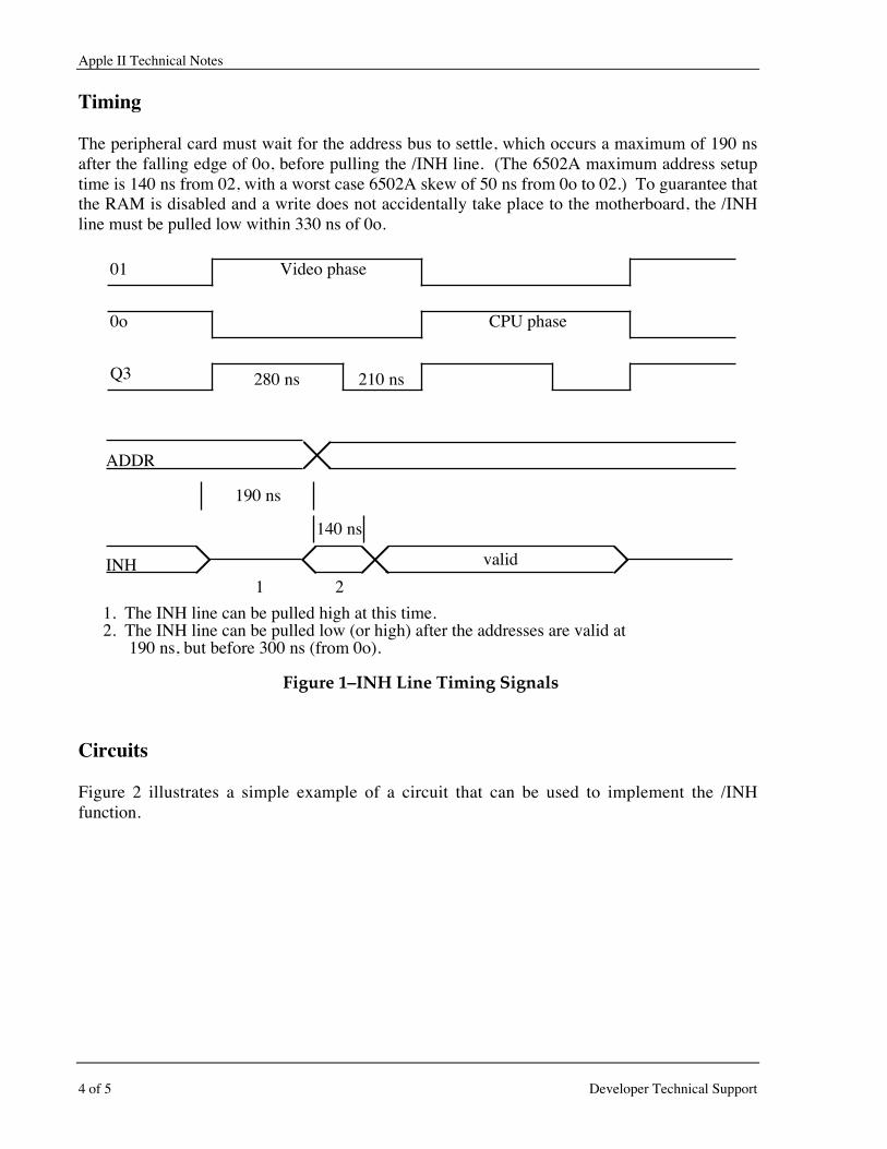
Apple II Technical Notes
4 of 5 Developer Technical Support
Timing
The peripheral card must wait for the address bus to settle, which occurs a maximum of 190 nsafter the falling edge of 0o, before pulling the /INH line. (The 6502A maximum address setuptime is 140 ns from 02, with a worst case 6502A skew of 50 ns from 0o to 02.) To guarantee thatthe RAM is disabled and a write does not accidentally take place to the motherboard, the /INHline must be pulled low within 330 ns of 0o.
ADDR
0o
01
Q3
CPU phase
Video phase
valid
Figure 1–INH Line Timing Signals
280 ns 210 ns
INH
190 ns
140 ns
1 2
1. The INH line can be pulled high at this time.2. The INH line can be pulled low (or high) after the addresses are valid at 190 ns, but before 300 ns (from 0o).
Circuits
Figure 2 illustrates a simple example of a circuit that can be used to implement the /INHfunction.
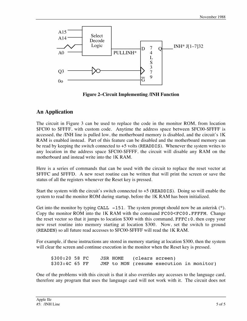
November 1988
Apple IIe#5: /INH Line 5 of 5
74LS379
A15
PULLINH*INH* J[1–7]32
SelectDecodeLogic
A14
A0
Q3
0o
D
G
Q
Figure 2–Circuit Implementing /INH Function
An Application
The circuit in Figure 3 can be used to replace the code in the monitor ROM, from location$FC00 to $FFFF, with custom code. Anytime the address space between $FC00-$FFFF isaccessed, the /INH line is pulled low, the motherboard memory is disabled, and the circuit’s 1KRAM is enabled instead. Part of this feature can be disabled and the motherboard memory canbe read by keeping the switch connected to +5 volts (READDIS). Whenever the system writes toany location in the address space $FC00-$FFFF, the circuit will disable any RAM on themotherboard and instead write into the 1K RAM.
Here is a series of commands that can be used with the circuit to replace the reset vector at$FFFC and $FFFD. A new reset routine can be written that will print the screen or save thestatus of all the registers whenever the Reset key is pressed.
Start the system with the circuit’s switch connected to +5 (READDIS). Doing so will enable thesystem to read the monitor ROM during startup, before the 1K RAM has been initialized.
Get into the monitor by typing CALL -151. The system prompt should now be an asterisk (*).Copy the monitor ROM into the 1K RAM with the command FC00<FC00.FFFFM. Changethe reset vector so that it jumps to location $300 with this command, FFFC:0, then copy yournew reset routine into memory starting at location $300. Now, set the switch to ground(READEN) so all future read accesses to $FC00-$FFFF will read the 1K RAM.
For example, if these instructions are stored in memory starting at location $300, then the systemwill clear the screen and continue execution in the monitor when the Reset key is pressed.
$300:20 58 FC JSR HOME (clears screen)$303:4C 65 FF JMP to MON (resume execution in monitor)
One of the problems with this circuit is that it also overrides any accesses to the language card,therefore any program that uses the language card will not work with it. The circuit does not
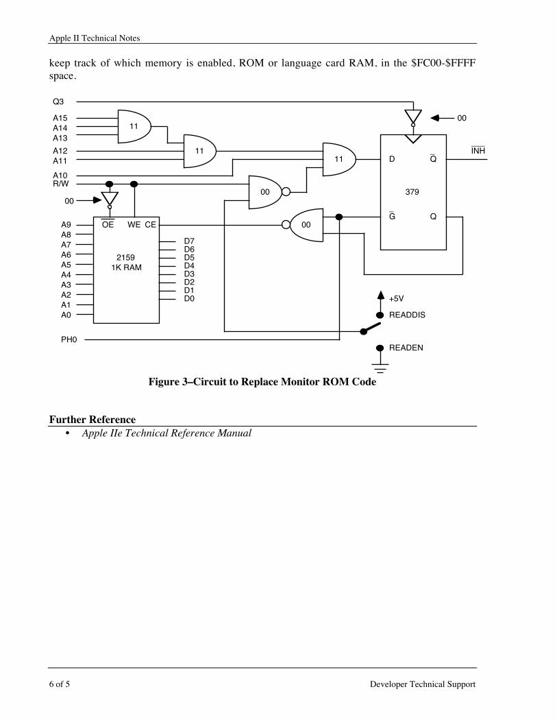
Apple II Technical Notes
6 of 5 Developer Technical Support
keep track of which memory is enabled, ROM or language card RAM, in the $FC00-$FFFFspace.
Q3
A15A14A13
A12A11
A10R/W
D Q_
QG_
379
+5V
READDIS
READEN
INH___
D7D6D5D4D3D2D1D0
00
00
1111
11
A9A8A7A6A5A4A3A2A1A0
OE
PH0
WE CE
2159 1K RAM
00
00
Figure 3–Circuit to Replace Monitor ROM Code
Further Reference• Apple IIe Technical Reference Manual
Apple IIe#6: The Apple II Paddle Circuits 1 of 5
Apple IITechnical Notes
Developer Technical SupportApple IIe#6: The Apple II Paddle Circuits
Revised by: Glenn A. Baxter November 1988Written by: Peter Baum May 1984
This Technical Note describes the paddle circuit used in the Apple II family of computers.
Caveats
Since Apple has introduced machines with internal clock speeds which may not be exactly 1.023MHz, it is best to use the PREAD firmware call to read paddle data. This Note assumes that theclock speed of the system is exactly 1.023 MHz. If you want to insure accuracy in readingpaddle data, you should make sure the system is first running at the correct speed. Enoughinformation is provided so that you can write your own PREAD routine, although this isdiscouraged. If the program runs on an Apple IIGS or some future machine, your custom paddlereading routine will fail to give the correct results.
Circuit Description
The value of the Apple paddles (or joystick) is determined by a software timing loop reading achange of state in a timing circuit. The paddles consist of a variable resistor (from 0-150k ohms)which makes up part of the timing circuit. There is a routine in the monitor ROM, calledPREAD, which counts the time until a state change occurs in the paddle circuit. This time istranslated into a value between 0 and 255.
The block diagrams in Figures 1 and 2 show the paddle circuit for the Apple ][+, Apple IIc, andthe Apple IIe. The large block on the left illustrates part of the circuitry inside the 558 timerchip. The 558 chip consists of four of these blocks, with all four paddle triggers lines shortedtogether on the motherboard and activated by the soft switch at $C070. The outputs of the 558chip run into a multiplexer, which places the appropriate signal onto the high bit of the data buswhen a paddle soft switch address in the range $C064 $C067 is read. The Apple IIc uses a 556timer rather than the 558 chip and only supports two paddles, 0 and 1.
The 100 ohm resistor and .022 microfarad capacitor are on the motherboard, with the variableresistor in the paddle. Each of the four paddle inputs have their own capacitor and resistor.Since these components can vary by as much as five percent from Apple to Apple, this circuit isnot a very exact analog to digital converter. If a paddle is moved from one Apple to another
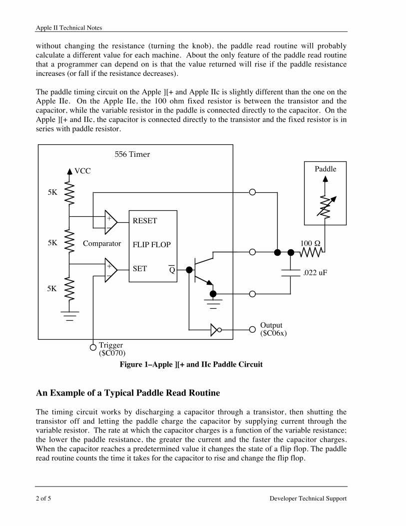
Apple II Technical Notes
2 of 5 Developer Technical Support
without changing the resistance (turning the knob), the paddle read routine will probablycalculate a different value for each machine. About the only feature of the paddle read routinethat a programmer can depend on is that the value returned will rise if the paddle resistanceincreases (or fall if the resistance decreases).
The paddle timing circuit on the Apple ][+ and Apple IIc is slightly different than the one on theApple IIe. On the Apple IIe, the 100 ohm fixed resistor is between the transistor and thecapacitor, while the variable resistor in the paddle is connected directly to the capacitor. On theApple ][+ and IIc, the capacitor is connected directly to the transistor and the fixed resistor is inseries with paddle resistor.
+–
+–
100
.022 uF
Output($C06x)
Paddle
RESET
FLIP FLOP
SET Q
Comparator
VCC
5K
5K
5K
Trigger($C070)
556 Timer
Figure 1–Apple ][+ and IIc Paddle Circuit
An Example of a Typical Paddle Read Routine
The timing circuit works by discharging a capacitor through a transistor, then shutting thetransistor off and letting the paddle charge the capacitor by supplying current through thevariable resistor. The rate at which the capacitor charges is a function of the variable resistance;the lower the paddle resistance, the greater the current and the faster the capacitor charges.When the capacitor reaches a predetermined value it changes the state of a flip flop. The paddleread routine counts the time it takes for the capacitor to rise and change the flip flop.
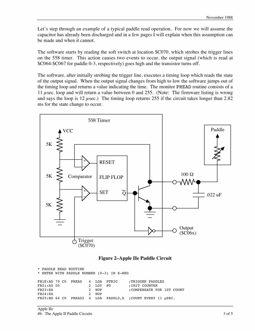
November 1988
Apple IIe#6: The Apple II Paddle Circuits 3 of 5
Let’s step through an example of a typical paddle read operation. For now we will assume thecapacitor has already been discharged and in a few pages I will explain when this assumption canbe made and when it cannot.
The software starts by reading the soft switch at location $C070, which strobes the trigger lineson the 558 timer. This action causes two events to occur, the output signal (which is read at$C064-$C067 for paddle 0-3, respectively) goes high and the transistor turns off.
The software, after initially strobing the trigger line, executes a timing loop which reads the stateof the output signal. When the output signal changes from high to low the software jumps out ofthe timing loop and returns a value indicating the time. The monitor PREAD routine consists of a11 µsec. loop and will return a value between 0 and 255. (Note: The firmware listing is wrongand says the loop is 12 µsec.) The timing loop returns 255 if the circuit takes longer than 2.82ms for the state change to occur.
+–
+–
100
.022 uF
Output($C06x)
Paddle
RESET
FLIP FLOP
SET Q
Comparator
VCC
5K
5K
5K
Trigger($C070)
558 Timer
Figure 2–Apple IIe Paddle Circuit
* PADDLE READ ROUTINE* ENTER WITH PADDLE NUMBER (0-3) IN X-REG
FB1E:AD 70 C0 PREAD 4 LDA PTRIG ;TRIGGER PADDLESFB21:A0 00 2 LDY #0 ;INIT COUNTERFB23:EA 2 NOP ;COMPENSATE FOR 1ST COUNTFB24:EA 2 NOPFB25:BD 64 C0 PREAD2 4 LDA PADDL0,X ;COUNT EVERY 11 µSEC.

Apple II Technical Notes
4 of 5 Developer Technical Support
FB28:10 04 2 BPL RTS2D ;BRANCH WHEN TIMED OUTFB2A:C8 2 INY ;INCREMENT COUNTERFB2B:D0 F8 3 BNE PREAD2 ;CONTINUE COUNTINGFB2D:88 DEY ;COUNTER OVERFLOWEDFB2E:60 RTS2D RTS ;RETURN W/VALUE 0-255
Inside the 558 timer chip, when the trigger is strobed low, the comparator that feeds the set inputof the flip flop is triggered, which in turn sets the output of the 558 timer. At the same time, thetransistor, which has held the capacitor near ground by sinking current from it, is shut off. Thecapacitor can now charge using the current supplied by the paddle. The smaller the paddle’sresistance, the more current the paddle will supply and the faster the capacitor charges. Aftersome time, the capacitor will charge to the threshold value of 3.3 volts, which is set by thevoltage divider network in the 558 timer, and the comparator that feeds the reset input on the flipflop will trigger. This trigger sets the output signal ($C06x) of the 558 timer low, whichindicates to the software that the circuit has timed out.
Trigger $C070
Output
ThresholdFeedback toReset Comp
Timing Value
0 – 2.82 milliseconds
Figure 3–Paddle Circuit Recharge Timing
Resetting the flip flop turns the transistor on, which discharges the capacitor very quickly(normally less than 250 ns). That paddle can then be read again.
A Closer Look at the Hardware
The First Anomaly
Notice that the last sentence states that the paddle can be read again and not the paddles. Ifanother paddle is read immediately after the first, it may yield the wrong value. To demonstratethis, I will step through an example of reading a second paddle immediately after finishing thefirst.
In this example I will assume that the first paddle has been set with a very low resistance, whilethe second paddle has a high resistance. The first paddle will time out very quickly and returnwith a small value, while the second paddle will take longer and yield a larger value.
We start reading the paddles by testing the paddle outputs to see if they are low, which indicatesthat the capacitor has been discharged. Assuming that the outputs are low, the next step is totrigger the 558 timer ($C070), which turns off the transistor and allows the capacitors to charge.Since all of the trigger input lines are shorted together, all four of the capacitors will charge, but
November 1988
Apple IIe#6: The Apple II Paddle Circuits 5 of 5
at different rates since the paddle resistances have been set to different values. The voltage onthe capacitor for the first paddle will reach the threshold voltage very quickly since the paddleresistance has been set low, therefore the timing loop will time out quickly.
At this point the capacitor for the second paddle is still charging and has not yet reached thethreshold since the paddle resistance was set to a high value. The transistor for the secondpaddle is still turned off due to the initial trigger used for reading paddle one. This means thatthe capacitor for the second paddle has not been discharged.
Any attempts at reading the second paddle now will only yield false results. The capacitor ispartly charged and therefore will reach the threshold value much faster than if the capacitor hadbeen completely discharged. If the timing loop is used, it will return with a smaller value than itwould if the capacitor had been completely discharged. Notice that retriggering (readinglocation $C070) the 558 timer will not help, since that only keeps the transistor turned off anddoes not help discharge the capacitor. The only way for the capacitor to discharge is to let thecircuit time out completely by letting the capacitor charge until it resets the flip flop.
To read the second paddle, the capacitor must first be discharged, which is only done when thethreshold value is reached and the 558 timer flip flop is reset. The only way to guarantee that thecapacitor is discharged is if the transistor is on. This condition is met when the paddle output islow. Therefore, start every paddle read either by waiting for at least 3 ms before strobing thetrigger input or testing to make sure that the paddle output is low.
If after 4 ms the paddle output is not low, then there is a good chance that there is no paddleconnected. This result may also indicate that a peripheral with a larger maximum value resistorthan the 150k ohms used by the Apple paddles is attached. Some peripheral devices use thistechnique of a larger variable resistor so that more than 256 points of resolution can bedetermined. Of course, this requires a custom software driver and the monitor PREAD routinecannot be used.
Apple IIe Anomalies
The problem with Apple IIe paddle input is that the capacitor may not be discharged by thetransistor. Typically, the transistor will discharge the capacitor in less than 250 ns on the Apple][+. But on the Apple IIe, if the paddle resistance is very low then the paddle may supplyenough current to always keep the capacitor charged.
Because the fixed resistor (100 ohms) on the Apple IIe motherboard is between the capacitor andthe transistor, there will be a voltage drop across the resistor if the capacitor stays charged.When the transistor is shut off by the trigger strobe, this voltage drop will disappear and thecapacitor, which may be near the threshold voltage, will trigger the reset comparator earlier thanit would if the capacitor had been discharged completely. The net affect of this is that thepaddles will read zero on the Apple IIe when they would read a small value on the Apple ][+ orIIc.
Other circuits which expect the capacitor to discharge completely may not work properly. Acircuit which attempts to simulate a paddle through active components such as a digital to analog
Apple II Technical Notes
6 of 5 Developer Technical Support
converter may be able to source enough current that the capacitor never discharges and thepaddle always reads zero.
It should also be noted that due to electromagnetic interference, later model IIe computersactually have an extra capacitor attached between the BUTTON inputs and ground. Thisessentially slows the response time of the input, making a fully digital input appear a bit moreanalog (no pun intended). Care should be taken in designing system which depend on a certainrepetition rate of the button inputs. Careful engineering and testing across systems shouldprevent any problems. As an example, adding a transistor output stage to drive the button inputsto the appropriate states might be a good idea for a serializing A/D. A joystick would not requirethis kind of circuit because the user input is too slow to be affected by the capacitors. For moreinformation on the changes in later model IIe computers, refer to Apple IIe Technical Note #9,Switch Input Changes.
Conclusion
Hopefully, this Note has given the reader a good feel for the paddle circuitry and the routineswhich determine the paddle values. To reinforce the material covered, you should try writingyour own paddle read routine. For example, you could write a read routine that would read twopaddles at once. The software loop will not have the 11 µsec. resolution of the PREAD routine,but you will find it still works just fine. Happy programming.
Further Reference• Apple IIe Technical Reference Manual

Apple IIe#7: Interfaces—Serial, Parallel, and IEEE–48 1 of 3
Apple IITechnical Notes
Developer Technical SupportApple IIe#7: Interfaces—Serial, Parallel, and IEEE–488
Revised by: Matt Deatherage November 1988Written by: Peter Baum April 1984
This Technical Note describes the pin configurations of three difference interface types offeredon the Apple II family of computers.
Serial
Currently, Apple sells a card, called the Super Serial Card (SSC), that can be used to connect anApple printer to an Apple II. The SSC replaces both the Communications Card and the Hi-SpeedSerial Card. The SSC supports the firmware (Pascal 1.1) protocol except for the optional controland interrupt handling routines.
The SSC has a 10-pin header on it, but comes with a cable which connects the header to a femaleDB-25 connector. The SSC can be configured as either a modem (DCE) or as a terminal (DTE)using a jumper block (in the latter case the jumper block acts as a modem eliminator). Thoughthe pin configuration of the DB-25 connector is well defined, there is no standard use of thehandshake signals. Different printers will use the handshake lines for different functions. Table1 shows the pin configuration for the DB-25 on the SSC. Consult your printer manual for morespecific information on which signals are used.
10-pin Female DB-25Header Signal Name Terminal Modem
1 Frame Ground (FRMGND) 1 12 Transmit Data (TxD) 3 23 Receive Data (RxD) 2 34 Request To Send (RTS) 8 45 Clear To Send (CTS) 8 56 Data Set Ready (DSR) 20 68 Signal Ground (SGLGND) 7 7
10 Data Carrier Detect (DCD) 4,5 *87 Secondary Clear to Send (SCTS) 19 **199 Data Terminal Ready (DTR) 6 20
* Only if SW1-7 is closed (on) with SSC.** Only if SW2-7 is closed (on) with SSC.
Apple II Technical Notes
2 of 3 Developer Technical Support
Table 1–Pin Configuration for SSC DB-25 Connector
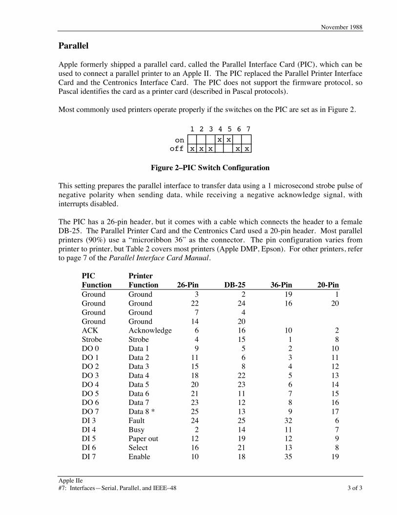
November 1988
Apple IIe#7: Interfaces—Serial, Parallel, and IEEE–48 3 of 3
Parallel
Apple formerly shipped a parallel card, called the Parallel Interface Card (PIC), which can beused to connect a parallel printer to an Apple II. The PIC replaced the Parallel Printer InterfaceCard and the Centronics Interface Card. The PIC does not support the firmware protocol, soPascal identifies the card as a printer card (described in Pascal protocols).
Most commonly used printers operate properly if the switches on the PIC are set as in Figure 2.
1 2 3 4 5 6 7
xxxx
xxxon
off
Figure 2–PIC Switch Configuration
This setting prepares the parallel interface to transfer data using a 1 microsecond strobe pulse ofnegative polarity when sending data, while receiving a negative acknowledge signal, withinterrupts disabled.
The PIC has a 26-pin header, but it comes with a cable which connects the header to a femaleDB-25. The Parallel Printer Card and the Centronics Card used a 20-pin header. Most parallelprinters (90%) use a “microribbon 36” as the connector. The pin configuration varies fromprinter to printer, but Table 2 covers most printers (Apple DMP, Epson). For other printers, referto page 7 of the Parallel Interface Card Manual.
PIC PrinterFunction Function 26-Pin DB-25 36-Pin 20-PinGround Ground 3 2 19 1Ground Ground 22 24 16 20Ground Ground 7 4Ground Ground 14 20ACK Acknowledge 6 16 10 2Strobe Strobe 4 15 1 8DO 0 Data 1 9 5 2 10DO 1 Data 2 11 6 3 11DO 2 Data 3 15 8 4 12DO 3 Data 4 18 22 5 13DO 4 Data 5 20 23 6 14DO 5 Data 6 21 11 7 15DO 6 Data 7 23 12 8 16DO 7 Data 8 * 25 13 9 17DI 3 Fault 24 25 32 6DI 4 Busy 2 14 11 7DI 5 Paper out 12 19 12 9DI 6 Select 16 21 13 8DI 7 Enable 10 18 35 19
Apple II Technical Notes
4 of 3 Developer Technical Support
** 7* This may be assigned a “hard” value for some printers to distinguish between
graphics and normal character sets.** Pin 7 is blocked on the female DB-25 connector and omitted on the mail DB-
25 connector to prevent the insertion of serial connectors into parallel ports.
IEEE-488
The IEEE-488 bus standard is a well defined eight-bit parallel, byte serial, asynchronous datatransfer interface. The standard has been thoroughly documented with the most completedescription available from the Institute of Electrical and Electronic Engineers (IEEE) in NewYork. Standard cables are manufactured by many companies and usually advertised as eitherIEEE-488, General Purpose Interface Bus (GPIB), or Hewlett-Packard Interface Bus (HPIB)cables.
IEEE-488 cards do not support Apple firmware protocols, so an assembly language driver mustbe used to access the cards from high level languages (see Appendix F of the IEEE-488 InterfaceUser’s Guide).
Further Reference• Apple IIe Technical Reference Manual• Parallel Interface Card Manual• IEEE–488 Card Manual
Apple IIe#8: Known Anomalies of Enhanced IIe ROMs 1 of 2
Apple IITechnical Notes
Developer Technical SupportApple IIe#8: Known Anomalies of Enhanced IIe ROMs
Revised by: Matt Deatherage November 1988Revised by: Cameron Birse February 1986
This Technical Note describes three problems with the Enhanced IIe ROMs and some suggestedsolutions.
The following three anomalies are known to occur when the Enhanced IIe ROMs are present:
1. Some Apple II peripheral cards do not handle interrupts well since Apple IIfamily members before the IIc and Enhanced IIe did not handle them very welleither. If a card that cannot handle interrupts is used on the Enhanced Apple IIe,any interrupt is very likely to crash the system. A common example of this wouldbe older, non-interruptible printer cards used with a Mouse card in the system.You can often work around this problem by disabling interrupts before printing tosuch a printer card.
2. There may be some problems when using the ROMs with communicationspackages. These problems are due to the way the 80-column firmware switchesinto 40-column mode. By sending a Control-Q through COUT, the firmwareswitches into 40-column mode. A simple solution to this would be to send anEscape-Control-D sequence, which disables the control functions. This solutionwill remain in effect until either the 80-column card is re-initialized by PR#3 oran Escape-Control-E sequence is sent through COUT. Another solution would beto simply not allow Control-Q sequences to get through to COUT by filtering thembefore they get there.
3. Many developers using double high-resolution graphics may wish to use 40-column text displays so the text can be read on a television set. There are acouple of possibilities:
A. You can define your own double high-resolution character set with any sizecharacters you desire, then plot them on the double high-resolution screen.
B. You can print text to the Apple IIe text screen and toggle the screen on todisplay it.

Apple II Technical Notes
2 of 2 Developer Technical Support
Note: There is no way to display four lines of 40-column text at the bottomof the double high-resolution screen in mixed mode since the 80-column hardware must be active while double high-resolution graphicsare being displayed.
November 1988
Apple IIe#8: Known Anomalies of Enhanced IIe ROMs 3 of 2
To use the second method, however, does require some special considerations.
The Apple IIe scroll routine continues to use the window parameters whenscrolling, but uses the 80COL soft switch to determine if it should scroll the80- or 40-column screen. Since the firmware has initialized a 40-columnwindow, the scroll routines will move only the first 40 columns. But, the80COL flag has been turned on for double high-resolution, therefore, thescrolling routine takes every even column from auxiliary memory and everyodd column from main memory. As a result, only the first 40 columns getscrolled, 20 columns from auxiliary memory and 20 columns from mainmemory.
One possible solution to the problem is to write your own scroll routines.Another might be to write to the screen so that scrolling will not occur. Butthere is yet another solution. Turn on the full 80-column mode with a PR#3or the equivalent. Now print your text to COUT in the normal manner, beingcareful not to exceed 40 characters per line. The 80 column firmware willscroll everything properly. When you are ready to display text, send aControl-Q sequence through COUT to switch to 40 columns. When you areready to return to double high-resolution mode, send a Control-R sequence toCOUT.
When switching modes, a momentary glitch may occur. If you send theControl-Q sequence to COUT while still in graphics mode, the screen will goto regular single high-resolution mode before finally going to text mode. Ifyou switch to text mode first, the text will be in 80-column mode (with 40columns displayed on the left half of the screen) before ultimately going to40-column mode. The same potential glitch may occur going back to doublehigh-resolution mode. The glitch will be only momentary and may notpresent any problem for your application.
Further Reference• Apple IIe Technical Reference Manual
Apple IIe#9: Switch Input Changes 1 of 3
Apple IITechnical Notes
Developer Technical SupportApple IIe#9: Switch Input Changes
Revised by: Glenn A. Baxter November 1988Written by: Earl Edwards May 1988
This Technical Note describes three changes which have been made to the switch circuitry ofApple IIe revision C and later motherboards.
The latest Apple IIe logic board has some changes in its switch circuitry. Logic boards with partnumbers 820-0087-C and later differ from earlier boards as follows:
• SW2 has been connected to the Shift keys on the keyboard by closing the X6jumper.
• 12k ohm pullup resistors have been added to SW0 and SW1.• A 0.1 microfarad capacitor to ground has been added to all three switch inputs:
SW0 (PB0, Open-Apple, OAPL), SW1 (PB1, Option, Closed-Apple, CAPL), andSW2 (PB2).
Differences are illustrated in Figures 1 and 2.
The X6 jumper was closed to allow the Shift key to be read directly, facilitating the shift-clickmouse selection feature in software products. Note that this change connects SW2 to +5Vthrough a 1k ohm resistor, and when a shift key is depressed, SW2 is at ground potential.
The 12k ohm resistors were added to ensure that the self-diagnostic test would run when thekeyboard is disconnected. The resistors have negligible influence when the keyboard isconnected.
The capacitors were added to reduce radiated emissions. This reduction was required because ofchanges in the memory configuration. As a result of the addition, the functional bandwidth ofthe inputs has been reduced; however, the input requirements of the 74LS251 have not changed.This addition may cause improper operation with peripheral devices that rely on high pushbutton repetition rates.
The minimum V(IH) to the 74LS251 remains 2.0V, but for improved noise margin, a minimumV(IH) of 2.4V is recommended. This requires a drive of about 6 ma to overcome the 470-ohm 5percent resistor on SW0 and SW1.
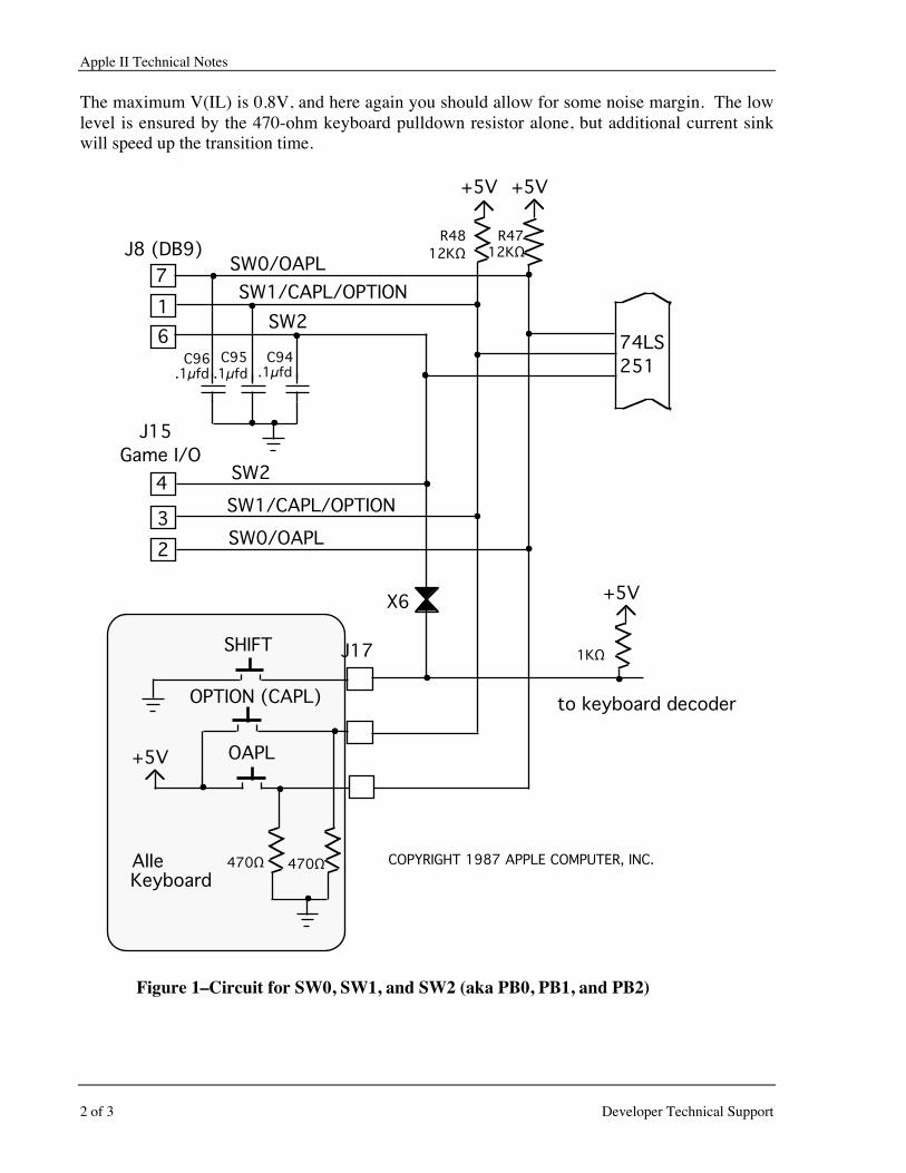
Apple II Technical Notes
2 of 3 Developer Technical Support
The maximum V(IL) is 0.8V, and here again you should allow for some noise margin. The lowlevel is ensured by the 470-ohm keyboard pulldown resistor alone, but additional current sinkwill speed up the transition time.
74LS
251
J8 (DB9)
J15
Game I/OSW2
SW1/CAPL/OPTION
SW0/OAPL
SW2
SW1/CAPL/OPTION
SW0/OAPL
C94C95C96.1µfd .1µfd .1µfd
X6
J17
Keyboard
+5V
+5V
SHIFT
OPTION (CAPL)
OAPL
470 470
1
7
6
+5V +5V
R47R4812K12K
to keyboard decoder
1K
4
3
2
COPYRIGHT 1987 APPLE COMPUTER, INC.AIIe
Figure 1–Circuit for SW0, SW1, and SW2 (aka PB0, PB1, and PB2)
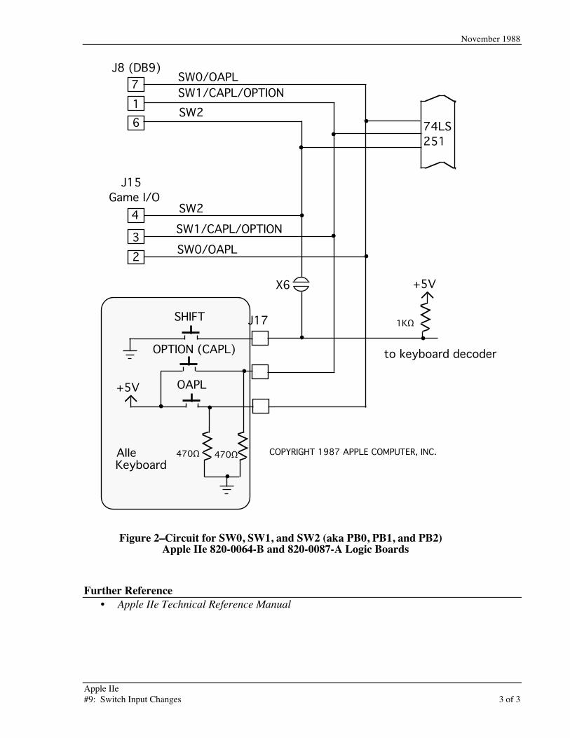
November 1988
Apple IIe#9: Switch Input Changes 3 of 3
74LS
251
J8 (DB9)
J15
Game I/OSW2
SW1/CAPL/OPTION
SW0/OAPL
SW1/CAPL/OPTION
SW0/OAPL
X6
J17
Keyboard
+5V
+5V
SHIFT
OPTION (CAPL)
OAPL
470 470
1
7
6
to keyboard decoder
1K
4
3
2
COPYRIGHT 1987 APPLE COMPUTER, INC.AIIe
SW2
Figure 2–Circuit for SW0, SW1, and SW2 (aka PB0, PB1, and PB2)Apple IIe 820-0064-B and 820-0087-A Logic Boards
Further Reference• Apple IIe Technical Reference Manual