appendix hardware description languages...
TRANSCRIPT
A
699
Hardware DescriptionLanguages
APPENDIX
A.1
Introduction
This appendix gives a quick introduction to the SystemVerilog and VHDL HardwareDescription Languages (HDLs). Many books treat HDLs as programming languages, butHDLs are better understood as a shorthand for describing digital hardware. It is best tobegin your design process by planning, on paper or in your mind, the hardware you want.(For example, the MIPS processor consists of an FSM controller and a datapath builtfrom registers, adders, multiplexers, etc.) Then, write the HDL code that implies thathardware to a synthesis tool. A common error among beginners is to write a programwithout thinking about the hardware that is implied. If you don’t know what hardware youare implying, you are almost certain to get something that you don’t want. Sometimes, thismeans extra latches appearing in your circuit in places you didn’t expect. Other times, itmeans that the circuit is much slower than required or it takes far more gates than it wouldif it were more carefully described.
The treatment in this appendix is unusual in that both SystemVerilog and VHDL arecovered together. Discussion of the languages is divided into two columns for literal side-by-side comparison with SystemVerilog on the left and VHDL on the right. When youread the appendix for the first time, focus on one language or the other. Once you knowone, you’ll quickly master the other if you need it. Religious wars have raged over whichHDL is superior. According to a large 2007 user survey [Cooley07], 73% of respondentsprimarily used Verilog/SystemVerilog and 20% primarily used VHDL, but 41% needed touse both on their project because of legacy code, intellectual property blocks, or becauseVerilog is better suited to netlists. Thus, many designers need to be bilingual and mostCAD tools handle both.
In our experience, the best way to learn an HDL is by example. HDLs have specificways of describing various classes of logic; these ways are called
idioms
. This appendix willteach you how to write the proper HDL idiom for each type of block and put the blockstogether to produce a working system. We focus on a
synthesizable subset
of HDL suffi-cient to describe any hardware function. When you need to describe a particular kind ofhardware, look for a similar example and adapt it to your purpose. The languages containmany other capabilities that are mostly beneficial for writing test fixtures and that arebeyond the scope of this book. We do not attempt to define all the syntax of the HDLsrigorously because that is deathly boring and because it tends to encourage thinking ofHDLs as programming languages, not shorthand for hardware. Be careful when experi-menting with other features in code that is intended to be synthesized. There are manyways to write HDL code whose behavior in simulation and synthesis differ, resulting inimproper chip operation or the need to fix bugs after synthesis is complete. The subset ofthe language covered here has been carefully selected to minimize such discrepancies.
Appendix A Hardware Description Languages
700
A.1.1 Modules
A block of hardware with inputs and outputs is called a
module
. An AND gate, a multiplexer,and a priority circuit are all examples of hardware modules. The two general styles fordescribing module functionality are
behavioral
and
structural
. Behavioral models describewhat a module does. Structural models describe how a module is built from simpler pieces; itis an application of hierarchy. The SystemVerilog and VHDL code in Example A.1 illustratebehavioral descriptions of a module computing a random Boolean function,
Y
=
ABC
+
ABC
+
ABC
. Each module has three inputs,
A
,
B
, and
C
, and one output,
Y
.
Verilog and SystemVerilog Verilog was developed by Gateway Design Automation as a propri-etary language for logic simulation in 1984. Gateway was acquiredby Cadence in 1989 and Verilog was made an open standard in1990 under the control of Open Verilog International. The languagebecame an IEEE standard in 1995 and was updated in 2001[IEEE1364-01]. In 2005, it was updated again with minor clarifica-tions; more importantly, SystemVerilog [IEEE 1800-2009] was intro-duced, which streamlines many of the annoyances of Verilog andadds high-level programming language features that have provenuseful in verification. This appendix uses some of SystemVerilog’sfeatures.
There are many texts on Verilog, but the IEEE standard itself isreadable as well as authoritative.
VHDLVHDL is an acronym for the VHSIC Hardware Description Language.In turn, VHSIC is an acronym for the Very High Speed IntegratedCircuits project. VHDL was originally developed in 1981 by theDepartment of Defense to describe the structure and function ofhardware. Its roots draw from the Ada programming language. TheIEEE standardized VHDL in 1987 and updated the standard severaltimes since [IEEE1076-08]. The language was first envisionedfor documentation, but quickly was adopted for simulation andsynthesis.
VHDL is heavily used by U.S. military contractors and Euro-pean companies. By some quirk of fate, it also has a majority of uni-versity users.
[Pedroni10] offers comprehensive coverage of the language.
SystemVerilog module sillyfunction(input logic a, b, c, output logic y);
assign y = ~a & ~b & ~c | a & ~b & ~c | a & ~b & c;endmodule
A module begins with a listing of the inputs and outputs. Theassign statement describes combinational logic. ~ indicates NOT,& indicates AND, and | indicates OR.
logic signals such as the inputs and outputs are Booleanvariables (0 or 1). They may also have floating and undefined valuesthat will be discussed in Section A.2.8.
The logic type was introduced in SystemVerilog. It super-sedes the reg type, which was a perennial source of confusion inVerilog. logic should be used everywhere except on nets withmultiple drivers, as will be explained in Section A.7.
VHDLlibrary IEEE; use IEEE.STD_LOGIC_1164.all;
entity sillyfunction is port(a, b, c: in STD_LOGIC; y: out STD_LOGIC);end;
architecture synth of sillyfunction isbegin y <= ((not a) and (not b) and (not c)) or (a and (not b) and (not c)) or (a and (not b) and c);end;
VHDL code has three parts: the library use clause, the entitydeclaration, and the architecture body. The library useclause is required and will be discussed in Section A.7. The entitydeclaration lists the module’s inputs and outputs. The architec-ture body defines what the module does.
VHDL signals such as inputs and outputs must have a type dec-laration. Digital signals should be declared to be STD_LOGIC type.STD_LOGIC signals can have a value of ‘0’ or ‘1,’ as well as floatingand undefined values that will be described in Section A.2.8. TheSTD_LOGIC type is defined in the IEEE.STD_LOGIC_1164library, which is why the library must be used.
VHDL lacks a good default order of operations, so Booleanequations should be parenthesized.
Example A.1
Combinational Logic
A.1 Introduction
701
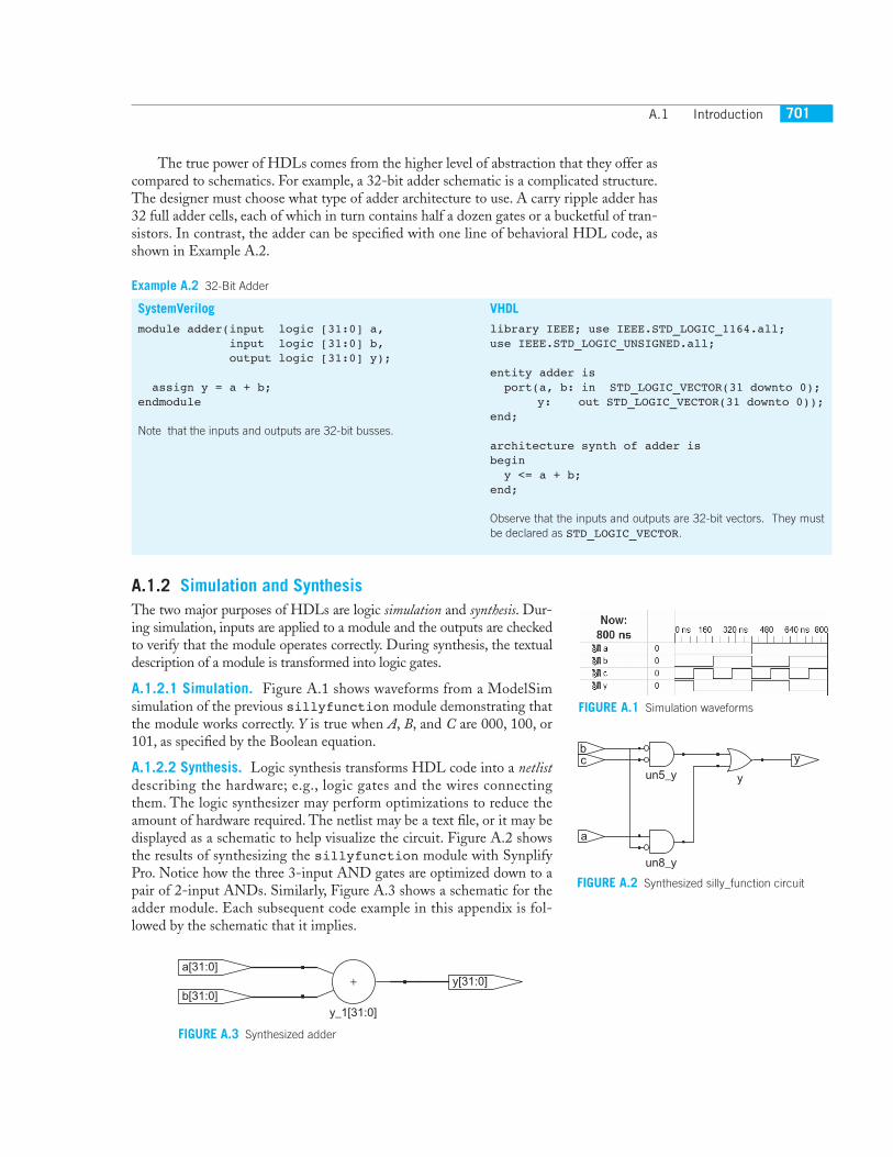
The true power of HDLs comes from the higher level of abstraction that they offer ascompared to schematics. For example, a 32-bit adder schematic is a complicated structure.The designer must choose what type of adder architecture to use. A carry ripple adder has32 full adder cells, each of which in turn contains half a dozen gates or a bucketful of tran-sistors. In contrast, the adder can be specified with one line of behavioral HDL code, asshown in Example A.2.
Example A.2
32-Bit Adder
A.1.2 Simulation and Synthesis
The two major purposes of HDLs are logic
simulation
and
synthesis
. Dur-ing simulation, inputs are applied to a module and the outputs are checkedto verify that the module operates correctly. During synthesis, the textualdescription of a module is transformed into logic gates.
A.1.2.1 Simulation.
Figure A.1 shows waveforms from a ModelSimsimulation of the previous
sillyfunction
module demonstrating thatthe module works correctly.
Y
is true when
A
,
B
, and
C
are 000, 100, or101, as specified by the Boolean equation.
A.1.2.2 Synthesis.
Logic synthesis transforms HDL code into a
netlist
describing the hardware; e.g., logic gates and the wires connectingthem. The logic synthesizer may perform optimizations to reduce theamount of hardware required. The netlist may be a text file, or it may bedisplayed as a schematic to help visualize the circuit. Figure A.2 showsthe results of synthesizing the
sillyfunction
module with SynplifyPro. Notice how the three 3-input AND gates are optimized down to apair of 2-input ANDs. Similarly, Figure A.3 shows a schematic for theadder module. Each subsequent code example in this appendix is fol-lowed by the schematic that it implies.
SystemVerilog module adder(input logic [31:0] a, input logic [31:0] b, output logic [31:0] y); assign y = a + b;endmodule
Note that the inputs and outputs are 32-bit busses.
VHDLlibrary IEEE; use IEEE.STD_LOGIC_1164.all;use IEEE.STD_LOGIC_UNSIGNED.all;
entity adder is port(a, b: in STD_LOGIC_VECTOR(31 downto 0); y: out STD_LOGIC_VECTOR(31 downto 0));end;
architecture synth of adder isbegin y <= a + b;end;
Observe that the inputs and outputs are 32-bit vectors. They mustbe declared as STD_LOGIC_VECTOR.
un5_y
un8_y
y
ycb
a
FIGURE A.2 Synthesized silly_function circuit
FIGURE A.1 Simulation waveforms
y_1[31:0]
+ y[31:0]b[31:0]
a[31:0]
FIGURE A.3 Synthesized adder
Appendix A Hardware Description Languages
702
A.2
Combinational Logic
The outputs of combinational logic depend only on the current inputs; combinationallogic has no memory. This section describes how to write behavioral models of combina-tional logic with HDLs.
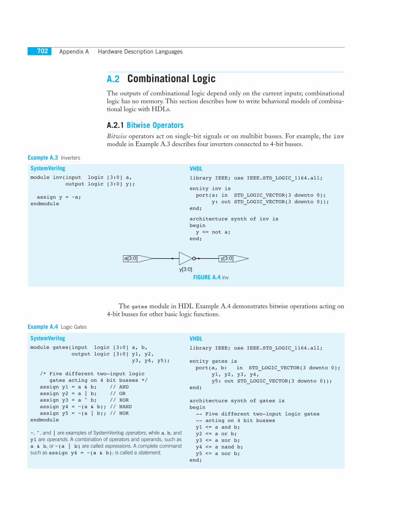
A.2.1 Bitwise Operators
Bitwise
operators act on single-bit signals or on multibit busses. For example, the
inv
module in Example A.3 describes four inverters connected to 4-bit busses.
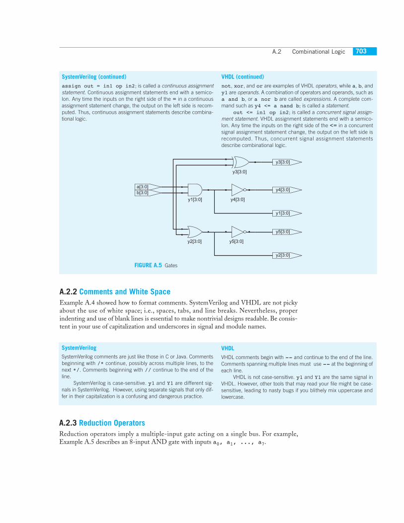
The
gates
module in HDL Example A.4 demonstrates bitwise operations acting on4-bit busses for other basic logic functions.
SystemVerilog
module inv(input logic [3:0] a, output logic [3:0] y);
assign y = ~a;endmodule
VHDLlibrary IEEE; use IEEE.STD_LOGIC_1164.all;
entity inv is port(a: in STD_LOGIC_VECTOR(3 downto 0); y: out STD_LOGIC_VECTOR(3 downto 0));end;
architecture synth of inv isbegin y <= not a;end;
y[3:0]
y[3:0]a[3:0]
FIGURE A.4 inv
Example A.3
Inverters
Example A.4
Logic Gates
SystemVerilog
module gates(input logic [3:0] a, b, output logic [3:0] y1, y2, y3, y4, y5);
/* Five different two-input logic gates acting on 4 bit busses */ assign y1 = a & b; // AND assign y2 = a | b; // OR assign y3 = a ^ b; // XOR assign y4 = ~(a & b); // NAND assign y5 = ~(a | b); // NORendmodule
~
,
^
, and | are examples of SystemVerilog operators, while a, b, andy1 are operands. A combination of operators and operands, such asa & b, or ~(a | b) are called expressions. A complete commandsuch as assign y4 = ~(a & b); is called a statement.
VHDLlibrary IEEE; use IEEE.STD_LOGIC_1164.all;
entity gates is port(a, b: in STD_LOGIC_VECTOR(3 downto 0); y1, y2, y3, y4, y5: out STD_LOGIC_VECTOR(3 downto 0));end;
architecture synth of gates isbegin -- Five different two-input logic gates -- acting on 4 bit busses y1 <= a and b; y2 <= a or b; y3 <= a xor b; y4 <= a nand b; y5 <= a nor b; end;
A.2 Combinational Logic 703
A.2.2 Comments and White SpaceExample A.4 showed how to format comments. SystemVerilog and VHDL are not pickyabout the use of white space; i.e., spaces, tabs, and line breaks. Nevertheless, properindenting and use of blank lines is essential to make nontrivial designs readable. Be consis-tent in your use of capitalization and underscores in signal and module names.
SystemVerilog (continued)assign out = in1 op in2; is called a continuous assignmentstatement. Continuous assignment statements end with a semico-lon. Any time the inputs on the right side of the = in a continuousassignment statement change, the output on the left side is recom-puted. Thus, continuous assignment statements describe combina-tional logic.
VHDL (continued)not, xor, and or are examples of VHDL operators, while a, b, andy1 are operands. A combination of operators and operands, such asa and b, or a nor b are called expressions. A complete com-mand such as y4 <= a nand b; is called a statement.
out <= in1 op in2; is called a concurrent signal assign-ment statement. VHDL assignment statements end with a semico-lon. Any time the inputs on the right side of the <= in a concurrentsignal assignment statement change, the output on the left side isrecomputed. Thus, concurrent signal assignment statementsdescribe combinational logic.
y1[3:0]
y2[3:0]
y3[3:0]
y4[3:0]
y5[3:0]
y5[3:0]
y4[3:0]
y3[3:0]
y2[3:0]
y1[3:0]
b[3:0]a[3:0]
FIGURE A.5 Gates
SystemVerilog
SystemVerilog comments are just like those in C or Java. Commentsbeginning with /* continue, possibly across multiple lines, to thenext */. Comments beginning with // continue to the end of theline.
SystemVerilog is case-sensitive. y1 and Y1 are different sig-nals in SystemVerilog. However, using separate signals that only dif-fer in their capitalization is a confusing and dangerous practice.
VHDLVHDL comments begin with -- and continue to the end of the line.Comments spanning multiple lines must use -- at the beginning ofeach line.
VHDL is not case-sensitive. y1 and Y1 are the same signal inVHDL. However, other tools that may read your file might be case-sensitive, leading to nasty bugs if you blithely mix uppercase andlowercase.
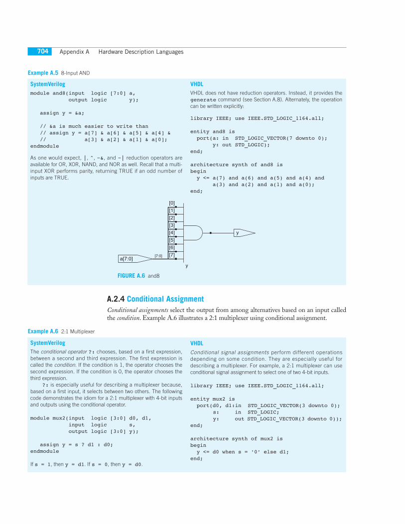
A.2.3 Reduction OperatorsReduction operators imply a multiple-input gate acting on a single bus. For example,Example A.5 describes an 8-input AND gate with inputs a0, a1, ..., a7.
Appendix A Hardware Description Languages704
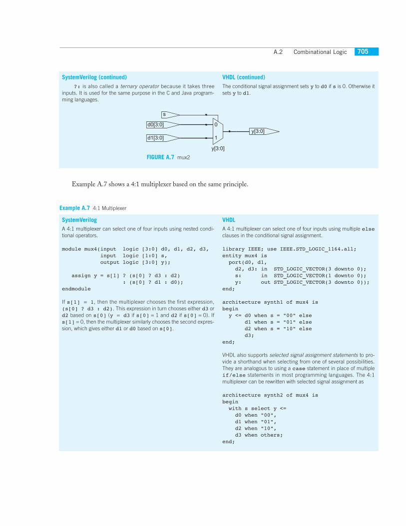
A.2.4 Conditional AssignmentConditional assignments select the output from among alternatives based on an input calledthe condition. Example A.6 illustrates a 2:1 multiplexer using conditional assignment.
y
y
a[7:0]
[0]
[1]
[2]
[3]
[4]
[5]
[6]
[7][7:0]
FIGURE A.6 and8
SystemVerilog
module and8(input logic [7:0] a, output logic y);
assign y = &a;
// &a is much easier to write than // assign y = a[7] & a[6] & a[5] & a[4] & // a[3] & a[2] & a[1] & a[0];endmodule
As one would expect, |, ^, ~&, and ~| reduction operators areavailable for OR, XOR, NAND, and NOR as well. Recall that a multi-input XOR performs parity, returning TRUE if an odd number ofinputs are TRUE.
VHDL
VHDL does not have reduction operators. Instead, it provides thegenerate command (see Section A.8). Alternately, the operationcan be written explicitly:
library IEEE; use IEEE.STD_LOGIC_1164.all;
entity and8 is port(a: in STD_LOGIC_VECTOR(7 downto 0); y: out STD_LOGIC);end;
architecture synth of and8 isbegin y <= a(7) and a(6) and a(5) and a(4) and a(3) and a(2) and a(1) and a(0);end;
Example A.5 8-Input AND
SystemVerilog
The conditional operator ?: chooses, based on a first expression,between a second and third expression. The first expression iscalled the condition. If the condition is 1, the operator chooses thesecond expression. If the condition is 0, the operator chooses thethird expression.
?: is especially useful for describing a multiplexer because,based on a first input, it selects between two others. The followingcode demonstrates the idiom for a 2:1 multiplexer with 4-bit inputsand outputs using the conditional operator.
module mux2(input logic [3:0] d0, d1, input logic s, output logic [3:0] y);
assign y = s ? d1 : d0; endmodule
If s = 1, then y = d1. If s = 0, then y = d0.
VHDLConditional signal assignments perform different operationsdepending on some condition. They are especially useful fordescribing a multiplexer. For example, a 2:1 multiplexer can useconditional signal assignment to select one of two 4-bit inputs.
library IEEE; use IEEE.STD_LOGIC_1164.all;
entity mux2 is port(d0, d1:in STD_LOGIC_VECTOR(3 downto 0);
s: in STD_LOGIC;y: out STD_LOGIC_VECTOR(3 downto 0));
end;
architecture synth of mux2 isbegin y <= d0 when s = '0' else d1;end;
Example A.6 2:1 Multiplexer
A.2 Combinational Logic 705
Example A.7 shows a 4:1 multiplexer based on the same principle.
y[3:0]
0
1y[3:0]
s
d1[3:0]
d0[3:0]
FIGURE A.7 mux2
SystemVerilog
A 4:1 multiplexer can select one of four inputs using nested condi-tional operators.
module mux4(input logic [3:0] d0, d1, d2, d3, input logic [1:0] s, output logic [3:0] y);
assign y = s[1] ? (s[0] ? d3 : d2) : (s[0] ? d1 : d0); endmodule
If s[1] = 1, then the multiplexer chooses the first expression,(s[0] ? d3 : d2). This expression in turn chooses either d3 ord2 based on s[0] (y = d3 if s[0] = 1 and d2 if s[0] = 0). Ifs[1] = 0, then the multiplexer similarly chooses the second expres-sion, which gives either d1 or d0 based on s[0].
VHDL
A 4:1 multiplexer can select one of four inputs using multiple elseclauses in the conditional signal assignment.
library IEEE; use IEEE.STD_LOGIC_1164.all;entity mux4 is port(d0, d1,
d2, d3: in STD_LOGIC_VECTOR(3 downto 0); s: in STD_LOGIC_VECTOR(1 downto 0);
y: out STD_LOGIC_VECTOR(3 downto 0));end;
architecture synth1 of mux4 isbegin y <= d0 when s = "00" else d1 when s = "01" else d2 when s = "10" else d3;end;
VHDL also supports selected signal assignment statements to pro-vide a shorthand when selecting from one of several possibilities.They are analogous to using a case statement in place of multipleif/else statements in most programming languages. The 4:1multiplexer can be rewritten with selected signal assignment as
architecture synth2 of mux4 isbegin with s select y <= d0 when "00", d1 when "01", d2 when "10", d3 when others;end;
Example A.7 4:1 Multiplexer
SystemVerilog (continued)?: is also called a ternary operator because it takes three
inputs. It is used for the same purpose in the C and Java program-ming languages.
VHDL (continued)The conditional signal assignment sets y to d0 if s is 0. Otherwise itsets y to d1.
Appendix A Hardware Description Languages706
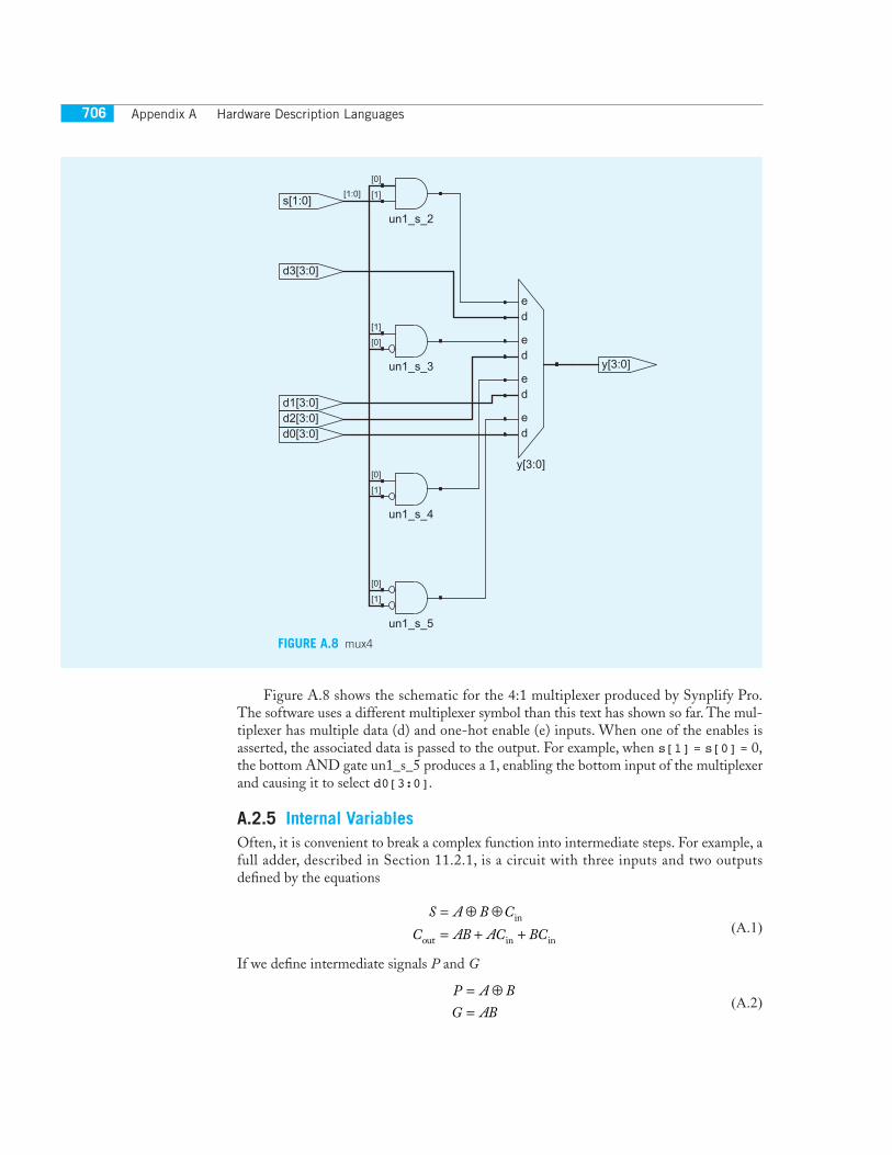
Figure A.8 shows the schematic for the 4:1 multiplexer produced by Synplify Pro.The software uses a different multiplexer symbol than this text has shown so far. The mul-tiplexer has multiple data (d) and one-hot enable (e) inputs. When one of the enables isasserted, the associated data is passed to the output. For example, when s[1] = s[0] = 0,the bottom AND gate un1_s_5 produces a 1, enabling the bottom input of the multiplexerand causing it to select d0[3:0].
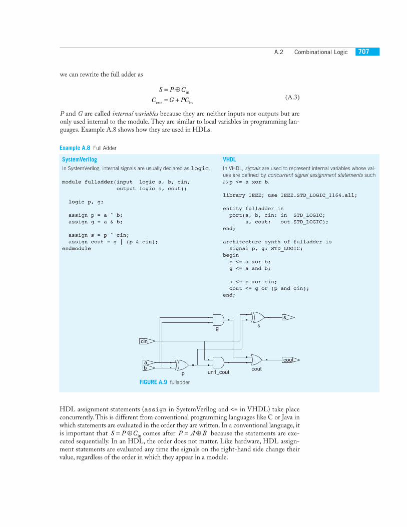
A.2.5 Internal VariablesOften, it is convenient to break a complex function into intermediate steps. For example, afull adder, described in Section 11.2.1, is a circuit with three inputs and two outputsdefined by the equations
(A.1)
If we define intermediate signals P and G
(A.2)
S A B C
C AB AC BC
= ⊕ ⊕= + +
in
out in in
P A B
G AB
= ⊕=
un1_s_2
un1_s_3
un1_s_4
un1_s_5
y[3:0]
ed
ed
ed
ed
y[3:0]
s[1:0][1:0]
d3[3:0]
d2[3:0]d1[3:0]
d0[3:0]
[0]
[1]
[1]
[0]
[0]
[1]
[0]
[1]
FIGURE A.8 mux4
A.2 Combinational Logic 707
we can rewrite the full adder as
(A.3)
P and G are called internal variables because they are neither inputs nor outputs but areonly used internal to the module. They are similar to local variables in programming lan-guages. Example A.8 shows how they are used in HDLs.
S P C
C G PC
= ⊕= +
in
out in
SystemVerilog
In SystemVerilog, internal signals are usually declared as logic.
module fulladder(input logic a, b, cin, output logic s, cout);
logic p, g;
assign p = a ^ b; assign g = a & b; assign s = p ^ cin; assign cout = g | (p & cin);endmodule
VHDL
In VHDL, signals are used to represent internal variables whose val-ues are defined by concurrent signal assignment statements suchas p <= a xor b.
library IEEE; use IEEE.STD_LOGIC_1164.all;
entity fulladder is port(a, b, cin: in STD_LOGIC; s, cout: out STD_LOGIC);end;
architecture synth of fulladder is signal p, g: STD_LOGIC;begin p <= a xor b; g <= a and b;
s <= p xor cin; cout <= g or (p and cin);end;
Example A.8 Full Adder
p
g s
un1_coutcout
cout
s
cin
ba
FIGURE A.9 fulladder
HDL assignment statements (assign in SystemVerilog and <= in VHDL) take placeconcurrently. This is different from conventional programming languages like C or Java inwhich statements are evaluated in the order they are written. In a conventional language, itis important that comes after because the statements are exe-cuted sequentially. In an HDL, the order does not matter. Like hardware, HDL assign-ment statements are evaluated any time the signals on the right-hand side change theirvalue, regardless of the order in which they appear in a module.
S P C= ⊕ in P A B= ⊕
Appendix A Hardware Description Languages708
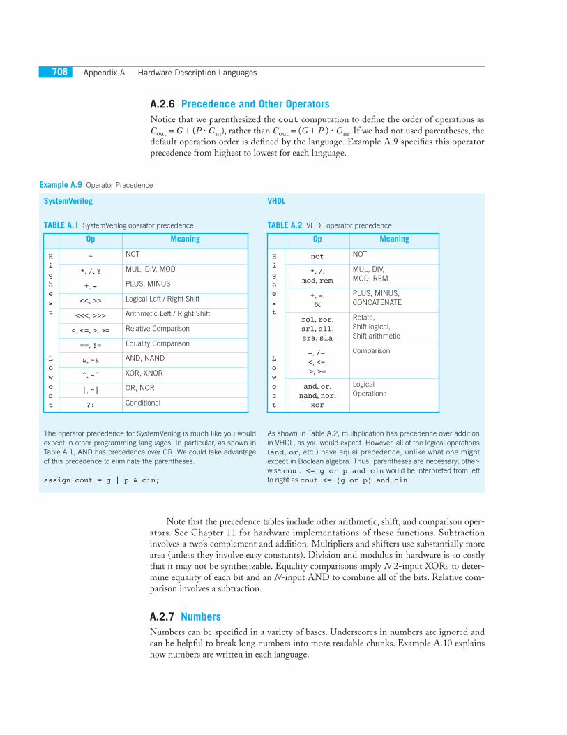
A.2.6 Precedence and Other OperatorsNotice that we parenthesized the cout computation to define the order of operations asCout = G + (P · C in), rather than Cout = (G + P ) · C in. If we had not used parentheses, thedefault operation order is defined by the language. Example A.9 specifies this operatorprecedence from highest to lowest for each language.
SystemVerilog
The operator precedence for SystemVerilog is much like you wouldexpect in other programming languages. In particular, as shown inTable A.1, AND has precedence over OR. We could take advantageof this precedence to eliminate the parentheses.
assign cout = g | p & cin;
VHDL
As shown in Table A.2, multiplication has precedence over additionin VHDL, as you would expect. However, all of the logical operations(and, or, etc.) have equal precedence, unlike what one mightexpect in Boolean algebra. Thus, parentheses are necessary; other-wise cout <= g or p and cin would be interpreted from leftto right as cout <= (g or p) and cin.
TABLE A.1 SystemVerilog operator precedence
Op Meaning
Highest
Lowest
~ NOT
*, /, % MUL, DIV, MOD
+, - PLUS, MINUS
<<, >> Logical Left / Right Shift
<<<, >>> Arithmetic Left / Right Shift
<, <=, >, >= Relative Comparison
==, != Equality Comparison
&, ~& AND, NAND
^, ~^ XOR, XNOR
|, ~| OR, NOR
?: Conditional
TABLE A.2 VHDL operator precedence
Op Meaning
Highest
Lowest
not NOT
*, /, mod, rem
MUL, DIV, MOD, REM
+, -, &
PLUS, MINUS, CONCATENATE
rol, ror,srl, sll, sra, sla
Rotate,Shift logical,Shift arithmetic
=, /=, <, <=, >, >=
Comparison
and, or, nand, nor,
xor
Logical Operations
Example A.9 Operator Precedence
Note that the precedence tables include other arithmetic, shift, and comparison oper-ators. See Chapter 11 for hardware implementations of these functions. Subtractioninvolves a two’s complement and addition. Multipliers and shifters use substantially morearea (unless they involve easy constants). Division and modulus in hardware is so costlythat it may not be synthesizable. Equality comparisons imply N 2-input XORs to deter-mine equality of each bit and an N-input AND to combine all of the bits. Relative com-parison involves a subtraction.
A.2.7 NumbersNumbers can be specified in a variety of bases. Underscores in numbers are ignored andcan be helpful to break long numbers into more readable chunks. Example A.10 explainshow numbers are written in each language.
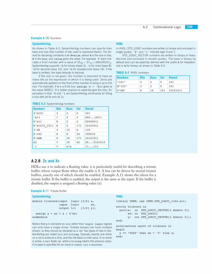
A.2 Combinational Logic 709
A.2.8 Zs and XsHDLs use z to indicate a floating value. z is particularly useful for describing a tristatebuffer, whose output floats when the enable is 0. A bus can be driven by several tristatebuffers, exactly one of which should be enabled. Example A.11 shows the idiom for atristate buffer. If the buffer is enabled, the output is the same as the input. If the buffer isdisabled, the output is assigned a floating value (z).
SystemVerilog
As shown in Table A.3, SystemVerilog numbers can specify theirbase and size (the number of bits used to represent them). The for-mat for declaring constants is N'Bvalue, where N is the size in bits,B is the base, and value gives the value. For example 9'h25 indi-cates a 9-bit number with a value of 2516 = 3710 = 0001001012.SystemVerilog supports 'b for binary (base 2), 'o for octal (base 8),'d for decimal (base 10), and 'h for hexadecimal (base 16). If thebase is omitted, the base defaults to decimal.
If the size is not given, the number is assumed to have asmany bits as the expression in which it is being used. Zeros areautomatically padded on the front of the number to bring it up to fullsize. For example, if w is a 6-bit bus, assign w = 'b11 gives wthe value 000011. It is better practice to explicitly give the size. Anexception is that '0 and '1 are SystemVerilog shorthands for fillinga bus with all 0s and all 1s.
VHDL
In VHDL, STD_LOGIC numbers are written in binary and enclosed insingle quotes. '0' and '1' indicate logic 0 and 1.
STD_LOGIC_VECTOR numbers are written in binary or hexa-decimal and enclosed in double quotes. The base is binary bydefault and can be explicitly defined with the prefix X for hexadeci-mal or B for binary, as shown in Table A.4.
TABLE A.3 SystemVerilog numbers
Numbers Bits Base Val Stored3'b101 3 2 5 101
'b11 ? 2 3 000...0011
8'b11 8 2 3 00000011
8'b1010_1011 8 2 171 10101011
3'd6 3 10 6 110
6'o42 6 8 34 100010
8'hAB 8 16 171 10101011
42 ? 10 42 00...0101010
'1 ? n/a 11...111
TABLE A.4 VHDL numbers
Numbers Bits Base Val Stored"101" 3 2 5 101
B"101" 3 2 5 101
X"AB" 8 16 161 10101011
Example A.10 Numbers
SystemVerilog
module tristate(input logic [3:0] a, input logic en, output tri [3:0] y);
assign y = en ? a : 4'bz;endmodule
Notice that y is declared as tri rather than logic. logic signalscan only have a single driver. Tristate busses can have multipledrivers, so they should be declared as a net. Two types of nets in Sys-temVerilog are called tri and trireg. Typically, exactly one driveron a net is active at a time, and the net takes on that value. If no driveris active, a tri floats (z), while a trireg retains the previous value.If no type is specified for an input or output, tri is assumed.
VHDL
library IEEE; use IEEE.STD_LOGIC_1164.all;
entity tristate is port(a: in STD_LOGIC_VECTOR(3 downto 0); en: in STD_LOGIC; y: out STD_LOGIC_VECTOR(3 downto 0));end;
architecture synth of tristate isbegin y <= "ZZZZ" when en = '0' else a;end;
Example A.11 Tristate Buffer
Appendix A Hardware Description Languages710
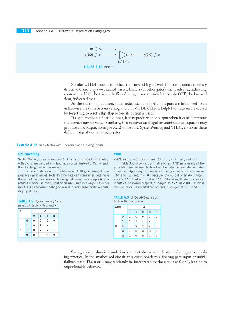
Similarly, HDLs use x to indicate an invalid logic level. If a bus is simultaneouslydriven to 0 and 1 by two enabled tristate buffers (or other gates), the result is x, indicatingcontention. If all the tristate buffers driving a bus are simultaneously OFF, the bus willfloat, indicated by z.
At the start of simulation, state nodes such as flip-flop outputs are initialized to anunknown state (x in SystemVerilog and u in VHDL). This is helpful to track errors causedby forgetting to reset a flip-flop before its output is used.
If a gate receives a floating input, it may produce an x output when it can’t determinethe correct output value. Similarly, if it receives an illegal or uninitialized input, it mayproduce an x output. Example A.12 shows how SystemVerilog and VHDL combine thesedifferent signal values in logic gates.
y_1[3:0]
y[3:0]
en
a[3:0]
FIGURE A.10 tristate
SystemVerilog
SystemVerilog signal values are 0, 1, z, and x. Constants startingwith z or x are padded with leading zs or xs (instead of 0s) to reachtheir full length when necessary.
Table A.5 shows a truth table for an AND gate using all fourpossible signal values. Note that the gate can sometimes determinethe output despite some inputs being unknown. For example 0 & zreturns 0 because the output of an AND gate is always 0 if eitherinput is 0. Otherwise, floating or invalid inputs cause invalid outputs,displayed as x.
VHDL
VHDL STD_LOGIC signals are '0', '1', 'z', 'x', and 'u'. Table A.6 shows a truth table for an AND gate using all five
possible signal values. Notice that the gate can sometimes deter-mine the output despite some inputs being unknown. For example,'0' and 'z' returns '0' because the output of an AND gate isalways '0' if either input is '0'. Otherwise, floating or invalidinputs cause invalid outputs, displayed as 'x' in VHDL. Uninitial-ized inputs cause uninitialized outputs, displayed as 'u' in VHDL.
TABLE A.5 SystemVerilog AND gate truth table with z and x
& A
0 1 z x
0 0 0 0 0
1 0 1 x x
B z 0 x x x
x 0 x x x
TABLE A.6 VHDL AND gate truth table with z, x, and u
AND A
0 1 z x u
0 0 0 0 0 0
1 0 1 x x u
B z 0 x x x u
x 0 x x x u
u 0 u u u u
Example A.12 Truth Tables with Undefined and Floating Inputs
Seeing x or u values in simulation is almost always an indication of a bug or bad cod-ing practice. In the synthesized circuit, this corresponds to a floating gate input or unini-tialized state. The x or u may randomly be interpreted by the circuit as 0 or 1, leading tounpredictable behavior.

A.2 Combinational Logic 711
A.2.9 Bit SwizzlingOften, it is necessary to operate on a subset of a bus or to concatenate, i.e., join together,signals to form busses. These operations are collectively known as bit swizzling. In Exam-ple A.13, y is given the 9-bit value c2c1d0d0d0c0101 using bit swizzling operations.
SystemVerilog
assign y = {c[2:1], {3{d[0]}}, c[0], 3'b101};
The {} operator is used to concatenate busses.{3{d[0]}} indicates three copies of d[0].Don’t confuse the 3-bit binary constant 3'b101 with bus b.
Note that it was critical to specify the length of 3 bits in the constant;otherwise, it would have had an unknown number of leading zerosthat might appear in the middle of y.
If y were wider than 9 bits, zeros would be placed in the mostsignificant bits.
VHDL
y <= c(2 downto 1) & d(0) & d(0) & d(0) & c(0) & "101";
The & operator is used to concatenate (join together) busses. ymust be a 9-bit STD_LOGIC_VECTOR. Do not confuse & with theand operator in VHDL.
Example A.13 Bit Swizzling
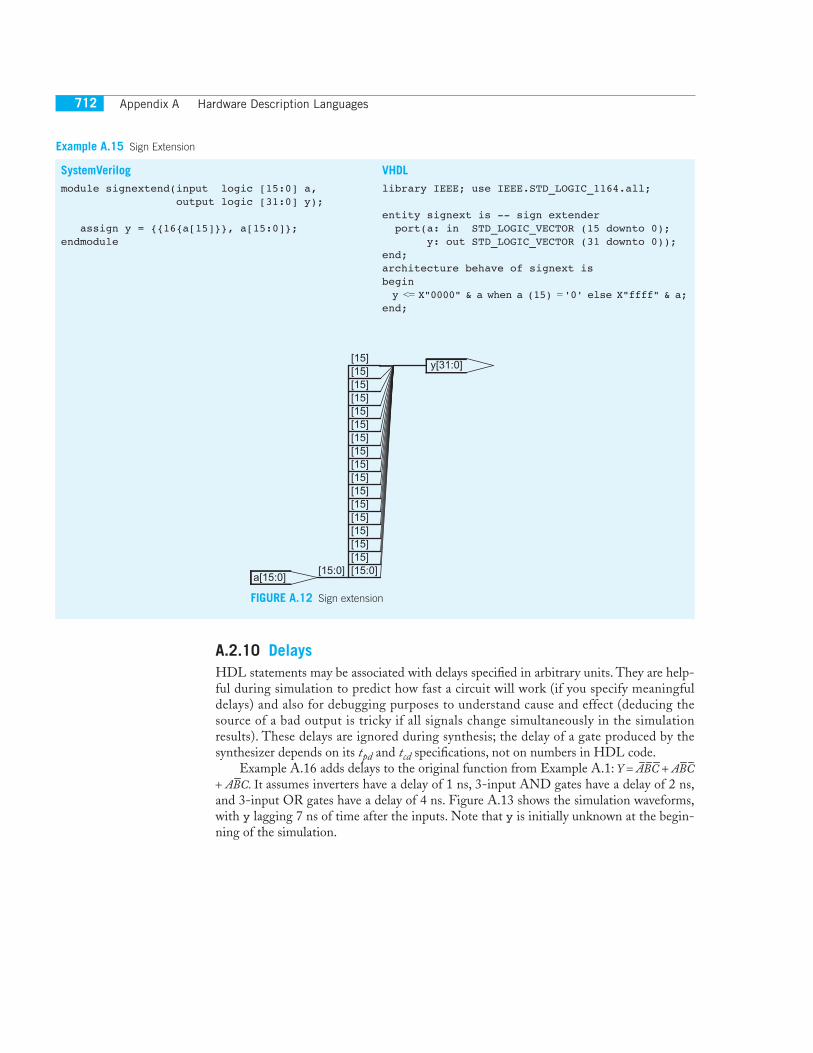
Example A.14 shows how to split an output into two pieces using bit swizzling andExample A.15 shows how to sign extend a 16-bit number to 32 bits by copying the mostsignificant bit into the upper 16 positions.
SystemVerilog
module mul(input logic [7:0] a, b, output logic [7:0] upper, lower);
assign {upper, lower} = a*b;endmodule
VHDL
library IEEE; use IEEE.STD_LOGIC_1164.all;use IEEE.STD_LOGIC_UNSIGNED.all;
entity mul is port(a, b: in STD_LOGIC_VECTOR(7 downto 0); upper, lower: out STD_LOGIC_VECTOR(7 downto 0));end;architecture behave of mul is signal prod: STD_LOGIC_VECTOR(15 downto 0);begin prod <= a * b; upper <= prod(15 downto 8); lower <= prod(7 downto 0);end;
Example A.14 Output Splitting
lower_1[15:0]
*
lower[7:0][7:0]
upper[7:0][15:8]
b[7:0]
a[7:0] [15:0]
FIGURE A.11 Multipliers
Appendix A Hardware Description Languages712
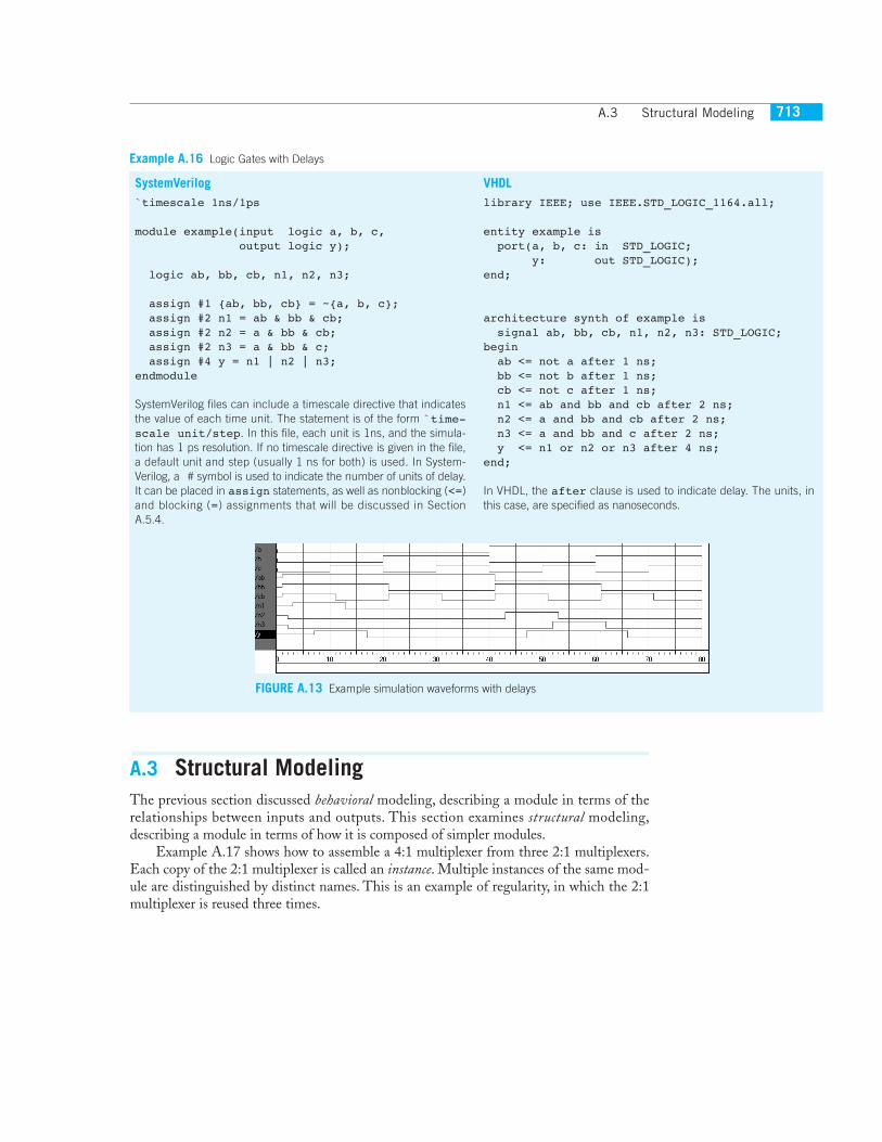
A.2.10 DelaysHDL statements may be associated with delays specified in arbitrary units. They are help-ful during simulation to predict how fast a circuit will work (if you specify meaningfuldelays) and also for debugging purposes to understand cause and effect (deducing thesource of a bad output is tricky if all signals change simultaneously in the simulationresults). These delays are ignored during synthesis; the delay of a gate produced by thesynthesizer depends on its tpd and tcd specifications, not on numbers in HDL code.
Example A.16 adds delays to the original function from Example A.1: Y = ABC + ABC+ ABC. It assumes inverters have a delay of 1 ns, 3-input AND gates have a delay of 2 ns,and 3-input OR gates have a delay of 4 ns. Figure A.13 shows the simulation waveforms,with y lagging 7 ns of time after the inputs. Note that y is initially unknown at the begin-ning of the simulation.
SystemVerilog
module signextend(input logic [15:0] a, output logic [31:0] y);
assign y = {{16{a[15]}}, a[15:0]};endmodule
VHDL
library IEEE; use IEEE.STD_LOGIC_1164.all;
entity signext is -- sign extender port(a: in STD_LOGIC_VECTOR (15 downto 0); y: out STD_LOGIC_VECTOR (31 downto 0));end;architecture behave of signext isbegin y <= X"0000" & a when a (15) = '0' else X"ffff" & a;end;
Example A.15 Sign Extension
y[31:0]
a[15:0][15:0]
[15][15][15][15][15][15][15][15][15][15][15][15][15][15][15][15][15:0]
FIGURE A.12 Sign extension
A.3 Structural Modeling 713
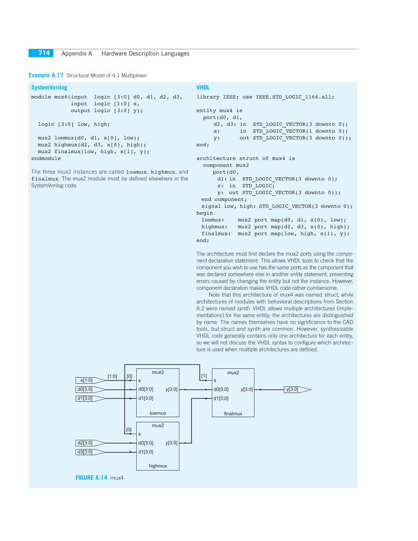
A.3 Structural ModelingThe previous section discussed behavioral modeling, describing a module in terms of therelationships between inputs and outputs. This section examines structural modeling,describing a module in terms of how it is composed of simpler modules.
Example A.17 shows how to assemble a 4:1 multiplexer from three 2:1 multiplexers.Each copy of the 2:1 multiplexer is called an instance. Multiple instances of the same mod-ule are distinguished by distinct names. This is an example of regularity, in which the 2:1multiplexer is reused three times.
SystemVerilog
`timescale 1ns/1ps
module example(input logic a, b, c, output logic y);
logic ab, bb, cb, n1, n2, n3;
assign #1 {ab, bb, cb} = ~{a, b, c}; assign #2 n1 = ab & bb & cb; assign #2 n2 = a & bb & cb; assign #2 n3 = a & bb & c; assign #4 y = n1 | n2 | n3;endmodule
SystemVerilog files can include a timescale directive that indicatesthe value of each time unit. The statement is of the form `time-scale unit/step. In this file, each unit is 1ns, and the simula-tion has 1 ps resolution. If no timescale directive is given in the file,a default unit and step (usually 1 ns for both) is used. In System-Verilog, a # symbol is used to indicate the number of units of delay.It can be placed in assign statements, as well as nonblocking (<=)and blocking (=) assignments that will be discussed in SectionA.5.4.
VHDL
library IEEE; use IEEE.STD_LOGIC_1164.all;
entity example is port(a, b, c: in STD_LOGIC; y: out STD_LOGIC);end;
architecture synth of example is signal ab, bb, cb, n1, n2, n3: STD_LOGIC;begin ab <= not a after 1 ns; bb <= not b after 1 ns; cb <= not c after 1 ns; n1 <= ab and bb and cb after 2 ns; n2 <= a and bb and cb after 2 ns; n3 <= a and bb and c after 2 ns; y <= n1 or n2 or n3 after 4 ns;end;
In VHDL, the after clause is used to indicate delay. The units, inthis case, are specified as nanoseconds.
Example A.16 Logic Gates with Delays
FIGURE A.13 Example simulation waveforms with delays
Appendix A Hardware Description Languages714
SystemVerilog
module mux4(input logic [3:0] d0, d1, d2, d3, input logic [1:0] s, output logic [3:0] y);
logic [3:0] low, high;
mux2 lowmux(d0, d1, s[0], low); mux2 highmux(d2, d3, s[0], high); mux2 finalmux(low, high, s[1], y);endmodule
The three mux2 instances are called lowmux, highmux, andfinalmux. The mux2 module must be defined elsewhere in theSystemVerilog code.
VHDL
library IEEE; use IEEE.STD_LOGIC_1164.all;
entity mux4 is port(d0, d1,
d2, d3: in STD_LOGIC_VECTOR(3 downto 0);s: in STD_LOGIC_VECTOR(1 downto 0);y: out STD_LOGIC_VECTOR(3 downto 0));
end;
architecture struct of mux4 is component mux2 port(d0,
d1: in STD_LOGIC_VECTOR(3 downto 0);s: in STD_LOGIC;y: out STD_LOGIC_VECTOR(3 downto 0));
end component;signal low, high: STD_LOGIC_VECTOR(3 downto 0);
beginlowmux: mux2 port map(d0, d1, s(0), low);highmux: mux2 port map(d2, d3, s(0), high);finalmux: mux2 port map(low, high, s(1), y);
end;
The architecture must first declare the mux2 ports using the compo-nent declaration statement. This allows VHDL tools to check that thecomponent you wish to use has the same ports as the component thatwas declared somewhere else in another entity statement, preventingerrors caused by changing the entity but not the instance. However,component declaration makes VHDL code rather cumbersome.
Note that this architecture of mux4 was named struct, whilearchitectures of modules with behavioral descriptions from SectionA.2 were named synth. VHDL allows multiple architectures (imple-mentations) for the same entity; the architectures are distinguishedby name. The names themselves have no significance to the CADtools, but struct and synth are common. However, synthesizableVHDL code generally contains only one architecture for each entity,so we will not discuss the VHDL syntax to configure which architec-ture is used when multiple architectures are defined.
Example A.17 Structural Model of 4:1 Multiplexer
mux2
lowmux
mux2
highmux
mux2
finalmux
y[3:0]
s[1:0][1:0]
d3[3:0]
d2[3:0]
d1[3:0]
d0[3:0]
[0]s
d0[3:0]
d1[3:0]
y[3:0]
[0]s
d0[3:0]
d1[3:0]
y[3:0]
[1]s
d0[3:0]
d1[3:0]
y[3:0]
FIGURE A.14 mux4
A.3 Structural Modeling 715
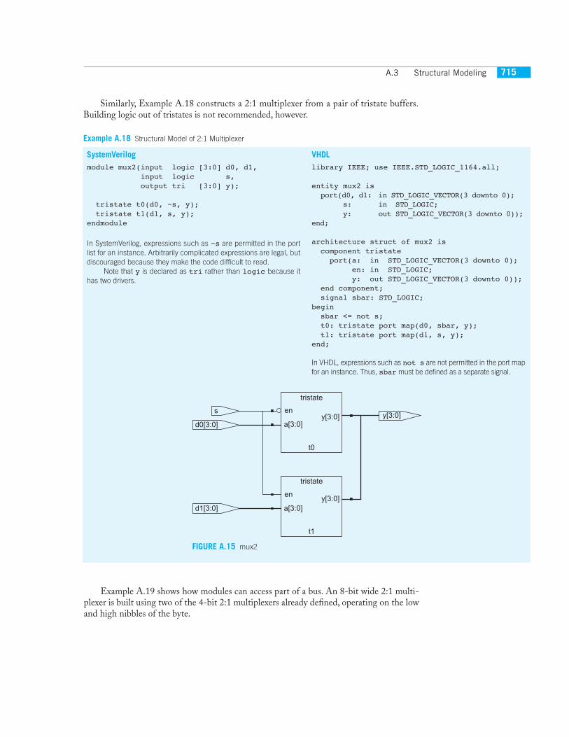
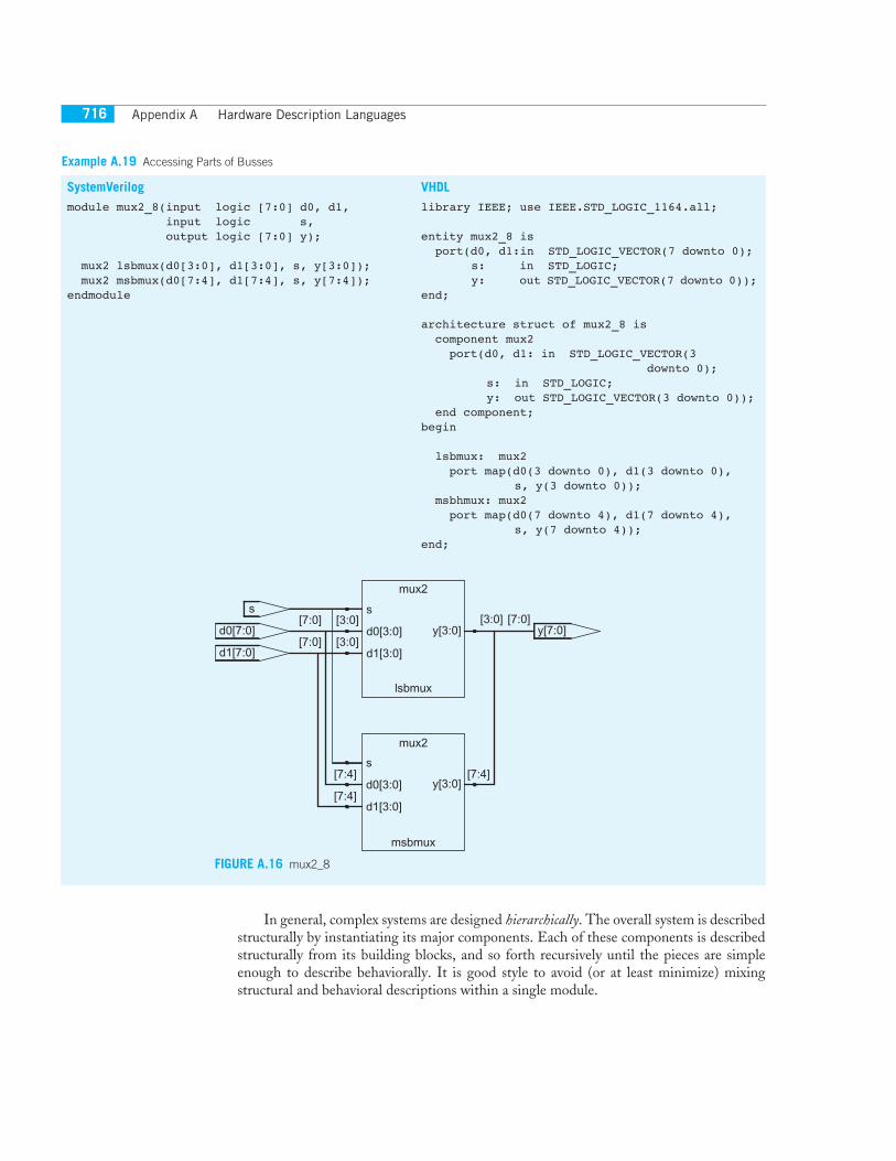
Example A.19 shows how modules can access part of a bus. An 8-bit wide 2:1 multi-plexer is built using two of the 4-bit 2:1 multiplexers already defined, operating on the lowand high nibbles of the byte.
SystemVerilog
module mux2(input logic [3:0] d0, d1, input logic s, output tri [3:0] y);
tristate t0(d0, ~s, y); tristate t1(d1, s, y);endmodule
In SystemVerilog, expressions such as ~s are permitted in the portlist for an instance. Arbitrarily complicated expressions are legal, butdiscouraged because they make the code difficult to read.
Note that y is declared as tri rather than logic because ithas two drivers.
VHDL
library IEEE; use IEEE.STD_LOGIC_1164.all;
entity mux2 is port(d0, d1: in STD_LOGIC_VECTOR(3 downto 0);
s: in STD_LOGIC;y: out STD_LOGIC_VECTOR(3 downto 0));
end;
architecture struct of mux2 is component tristate port(a: in STD_LOGIC_VECTOR(3 downto 0); en: in STD_LOGIC; y: out STD_LOGIC_VECTOR(3 downto 0)); end component; signal sbar: STD_LOGIC;begin sbar <= not s; t0: tristate port map(d0, sbar, y); t1: tristate port map(d1, s, y); end;
In VHDL, expressions such as not s are not permitted in the port mapfor an instance. Thus, sbar must be defined as a separate signal.
Example A.18 Structural Model of 2:1 Multiplexer
Similarly, Example A.18 constructs a 2:1 multiplexer from a pair of tristate buffers.Building logic out of tristates is not recommended, however.
tristate
t0
tristate
t1
y[3:0]s
d1[3:0]
d0[3:0]
en
a[3:0]y[3:0]
en
a[3:0]y[3:0]
FIGURE A.15 mux2
Appendix A Hardware Description Languages716
In general, complex systems are designed hierarchically. The overall system is describedstructurally by instantiating its major components. Each of these components is describedstructurally from its building blocks, and so forth recursively until the pieces are simpleenough to describe behaviorally. It is good style to avoid (or at least minimize) mixingstructural and behavioral descriptions within a single module.
SystemVerilog
module mux2_8(input logic [7:0] d0, d1, input logic s, output logic [7:0] y);
mux2 lsbmux(d0[3:0], d1[3:0], s, y[3:0]); mux2 msbmux(d0[7:4], d1[7:4], s, y[7:4]);endmodule
VHDL
library IEEE; use IEEE.STD_LOGIC_1164.all;
entity mux2_8 is port(d0, d1:in STD_LOGIC_VECTOR(7 downto 0);
s: in STD_LOGIC;y: out STD_LOGIC_VECTOR(7 downto 0));
end;
architecture struct of mux2_8 is component mux2 port(d0, d1: in STD_LOGIC_VECTOR(3 downto 0);
s: in STD_LOGIC;y: out STD_LOGIC_VECTOR(3 downto 0));
end component;begin
lsbmux: mux2 port map(d0(3 downto 0), d1(3 downto 0),
s, y(3 downto 0)); msbhmux: mux2 port map(d0(7 downto 4), d1(7 downto 4),
s, y(7 downto 4));end;
Example A.19 Accessing Parts of Busses
mux2
lsbmux
mux2
msbmux
y[7:0][7:0]
s
d1[7:0][7:0]
d0[7:0][7:0]
s[3:0]
d0[3:0][3:0]
d1[3:0]
[3:0]y[3:0]
s[7:4]
d0[3:0][7:4]
d1[3:0]
[7:4]y[3:0]
FIGURE A.16 mux2_8
A.4 Sequential Logic 717
A.4 Sequential LogicHDL synthesizers recognize certain idioms and turn them into specific sequential circuits.Other coding styles may simulate correctly, but synthesize into circuits with blatant orsubtle errors. This section presents the proper idioms to describe registers and latches.
A.4.1 RegistersThe vast majority of modern commercial systems are built with registers using positiveedge-triggered D flip-flops. Example A.20 shows the idiom for such flip-flops.
SystemVerilog
module flop(input logic clk, input logic [3:0] d, output logic [3:0] q);
always_ff @(posedge clk) q <= d;endmodule
A Verilog always statement is written in the form always @(sensitivity list) statement;
The statement is executed only when the event specified in the sensi-tivity list occurs. In this example, the statement is q <= d (pro-nounced “q gets d”). Hence, the flip-flop copies d to q on the positiveedge of the clock and otherwise remembers the old state of q.
<= is called a nonblocking assignment. Think of it as a regular= sign for now; we’ll return to the more subtle points in SectionA.5.4. Note that <= is used instead of assign inside an alwaysstatement.
As will be seen in subsequent sections, always statementscan be used to imply flip-flops, latches, or combinational logic,depending on the sensitivity list and statement. Because of this flex-ibility, it is easy to produce the wrong hardware inadvertently. Sys-temVerilog introduces always_ff , always_latch , andalways_comb to reduce the risk of common errors. always_ffbehaves like always, but is used exclusively to imply flip-flops andallows tools to produce a warning if anything else is implied.
VHDL
library IEEE; use IEEE.STD_LOGIC_1164.all;
entity flop is port(clk: in STD_LOGIC; d: in STD_LOGIC_VECTOR(3 downto 0); q: out STD_LOGIC_VECTOR(3 downto 0));end;
architecture synth of flop isbegin process(clk) begin if clk'event and clk = '1' then q <= d; end if; end process;end;
A VHDL process is written in the form process(sensitivity list) begin statement;end process;
The statement is executed when any of the variables in the sensitiv-ity list change. In this example, the if statement is executed whenclk changes, indicated by clk'event. If the change is a risingedge (clk = '1' after the event), then q <= d. Hence, the flip-flop copies d to q on the positive edge of the clock and otherwiseremembers the old state of q.
An alternative VHDL idiom for a flip-flop is process(clk) begin if RISING_EDGE(clk) then q <= d; end if;end process;
RISING_EDGE(clk) is synonymous with clk'event and clk= '1'.
Example A.20 Register
Appendix A Hardware Description Languages718
In SystemVerilog always statements and VHDL process statements, signals keeptheir old value until an event takes place that explicitly causes them to change. Hence,such code, with appropriate sensitivity lists, can be used to describe sequential circuits withmemory. For example, the flip-flop only includes clk in the sensitivity list. It remembersits old value of q until the next rising edge of the clk, even if d changes in the interim.
In contrast, SystemVerilog continuous assignment statements and VHDL concurrentassignment statements are reevaluated any time any of the inputs on the right-hand sidechanges. Therefore, such code necessarily describes combinational logic.
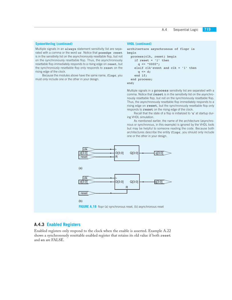
A.4.2 Resettable RegistersWhen simulation begins or power is first applied to a circuit, the output of the flop isunknown. This is indicated with x in SystemVerilog and 'u' in VHDL. Generally, it isgood practice to use resettable registers so that on power up you can put your system in aknown state. The reset may be either synchronous or asynchronous. Recall that synchro-nous reset occurs on the rising edge of the clock, while asynchronous reset occurs immedi-ately. Example A.21 demonstrates the idioms for flip-flops with synchronous andasynchronous resets. Note that distinguishing synchronous and asynchronous reset in aschematic can be difficult. The schematic produced by Synplify Pro places synchronousreset on the left side of a flip-flop and synchronous reset at the bottom.
Synchronous reset takes fewer transistors and reduces the risk of timing problems onthe trailing edge of reset. However, if clock gating is used, care must be taken that all flip-flops reset properly at startup.
q[3:0]d[3:0]clk
Q[3:0]D[3:0]
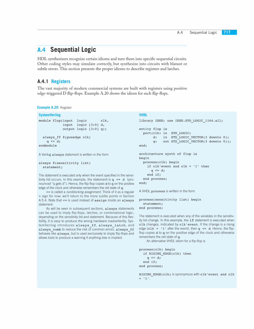
FIGURE A.17 flop
SystemVerilog
module flopr(input logic clk, input logic reset, input logic [3:0] d, output logic [3:0] q);
// synchronous reset always_ff @(posedge clk) if (reset) q <= 4'b0; else q <= d;endmodule
module flopr(input logic clk, input logic reset, input logic [3:0] d, output logic [3:0] q); // asynchronous reset always_ff @(posedge clk, posedge reset) if (reset) q <= 4'b0; else q <= d;endmodule
VHDL
library IEEE; use IEEE.STD_LOGIC_1164.all;
entity flopr is port(clk, reset: in STD_LOGIC; d: in STD_LOGIC_VECTOR(3 downto 0); q: out STD_LOGIC_VECTOR(3 downto 0));end;
architecture synchronous of flopr isbegin process(clk) begin if clk'event and clk = '1' then if reset = '1' then q <= "0000"; else q <= d; end if; end if; end process;end;
Example A.21 Resettable Register
A.4 Sequential Logic 719
A.4.3 Enabled RegistersEnabled registers only respond to the clock when the enable is asserted. Example A.22shows a synchronously resettable enabled register that retains its old value if both resetand en are FALSE.
SystemVerilog (continued) Multiple signals in an always statement sensitivity list are sepa-rated with a comma or the word or. Notice that posedge resetis in the sensitivity list on the asynchronously resettable flop, but noton the synchronously resettable flop. Thus, the asynchronouslyresettable flop immediately responds to a rising edge on reset, butthe synchronously resettable flop only responds to reset on therising edge of the clock.
Because the modules above have the same name, flopr, youmust only include one or the other in your design.
VHDL (continued) architecture asynchronous of flopr isbegin process(clk, reset) begin if reset = '1' then q <= "0000"; elsif clk'event and clk = '1' then q <= d; end if; end process;end;
Multiple signals in a process sensitivity list are separated with acomma. Notice that reset is in the sensitivity list on the asynchro-nously resettable flop, but not on the synchronously resettable flop.Thus, the asynchronously resettable flop immediately responds to arising edge on reset, but the synchronously resettable flop onlyresponds to reset on the rising edge of the clock.
Recall that the state of a flop is initialized to ‘u’ at startup dur-ing VHDL simulation.
As mentioned earlier, the name of the architecture (asynchro-nous or synchronous, in this example) is ignored by the VHDL toolsbut may be helpful to someone reading the code. Because botharchitectures describe the entity flopr, you should only includeone or the other in your design.
FIGURE A.18 flopr (a) synchronous reset, (b) asynchronous reset
q[3:0]d[3:0]reset
clkQ[3:0]D[3:0]
R
(a)
R
q[3:0]d[3:0]
reset
clkQ[3:0]D[3:0]
(b)
Appendix A Hardware Description Languages720
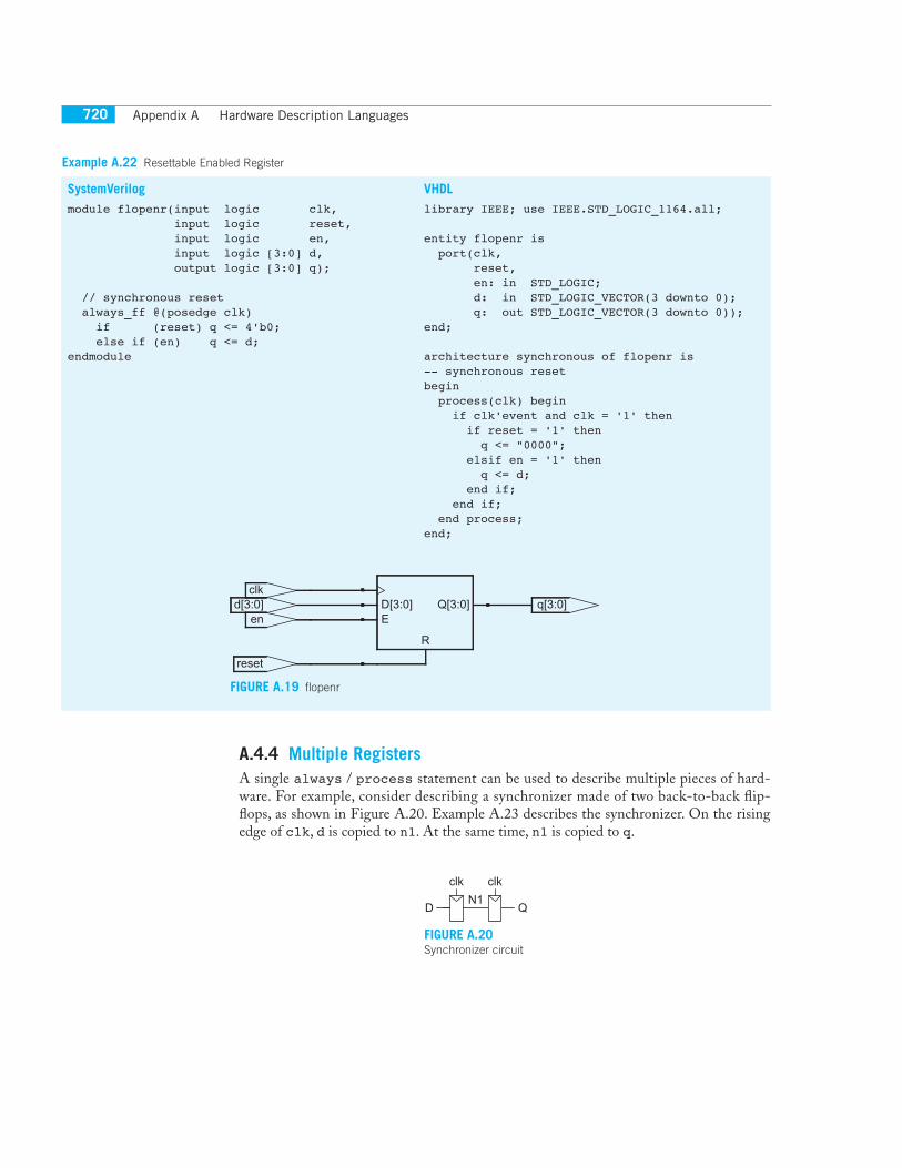
A.4.4 Multiple RegistersA single always / process statement can be used to describe multiple pieces of hard-ware. For example, consider describing a synchronizer made of two back-to-back flip-flops, as shown in Figure A.20. Example A.23 describes the synchronizer. On the risingedge of clk, d is copied to n1. At the same time, n1 is copied to q.
SystemVerilog
module flopenr(input logic clk, input logic reset, input logic en, input logic [3:0] d, output logic [3:0] q);
// synchronous reset always_ff @(posedge clk) if (reset) q <= 4'b0; else if (en) q <= d;endmodule
VHDL
library IEEE; use IEEE.STD_LOGIC_1164.all;
entity flopenr is port(clk, reset, en: in STD_LOGIC; d: in STD_LOGIC_VECTOR(3 downto 0); q: out STD_LOGIC_VECTOR(3 downto 0));end;
architecture synchronous of flopenr is -- synchronous resetbegin process(clk) begin if clk'event and clk = '1' then if reset = '1' then q <= "0000"; elsif en = '1' then q <= d; end if; end if; end process;end;
Example A.22 Resettable Enabled Register
R
q[3:0]d[3:0]en
reset
clkQ[3:0]D[3:0]
E
FIGURE A.19 flopenr
clk clk
D QN1
FIGURE A.20 Synchronizer circuit

A.4 Sequential Logic 721
A.4.5 LatchesRecall that a D latch is transparent when the clock is HIGH, allowing data to flow frominput to output. The latch becomes opaque when the clock is LOW, retaining its old state.Example A.24 shows the idiom for a D latch.
SystemVerilog
module sync(input logic clk, input logic d, output logic q);
logic n1;
always_ff @(posedge clk) begin n1 <= d; q <= n1; endendmodule
VHDL
library IEEE; use IEEE.STD_LOGIC_1164.all;
entity sync is port(clk: in STD_LOGIC; d: in STD_LOGIC; q: out STD_LOGIC);end;
architecture synth of sync is signal n1: STD_LOGIC;begin process(clk) begin if clk'event and clk = '1' then n1 <= d; q <= n1; end if; end process;end;
Example A.23 Synchronizer
SystemVerilog
module latch(input logic clk, input logic [3:0] d, output logic [3:0] q);
always_latch if (clk) q <= d;endmodule
always_latch is equivalent to always @(clk, d) and is thepreferred way of describing a latch in SystemVerilog. It evaluates anytime clk or d changes. If clk is HIGH, d flows through to q, so thiscode describes a positive level sensitive latch. Otherwise, q keeps itso ld va lue. SystemVer i log can generate a warn ing i f thealways_latch block doesn’t imply a latch.
VHDL
library IEEE; use IEEE.STD_LOGIC_1164.all;
entity latch is port(clk: in STD_LOGIC; d: in STD_LOGIC_VECTOR(3 downto 0); q: out STD_LOGIC_VECTOR(3 downto 0));end;
architecture synth of latch isbegin process(clk, d) begin if clk = '1' then q <= d; end if; end process;end;
The sensitivity list contains both clk and d, so the process evalu-ates any time clk or d changes. If clk is HIGH, d flows through to q.
Example A.24 D Latch
n1 q
qdclk
QD QD
FIGURE A.21 sync
Appendix A Hardware Description Languages722
Not all synthesis tools support latches well. Unless you know that your tool supportslatches and you have a good reason to use them, avoid them and use edge-triggered flip-flops instead. Furthermore, take care that your HDL does not imply any unintendedlatches, something that is easy to do if you aren't attentive. Many synthesis tools warn youif a latch is created; if you didn’t expect one, track down the bug in your HDL. And if youdon’t know whether you intended to have a latch or not, you are probably approachingHDLs like programming languages and have bigger problems lurking.
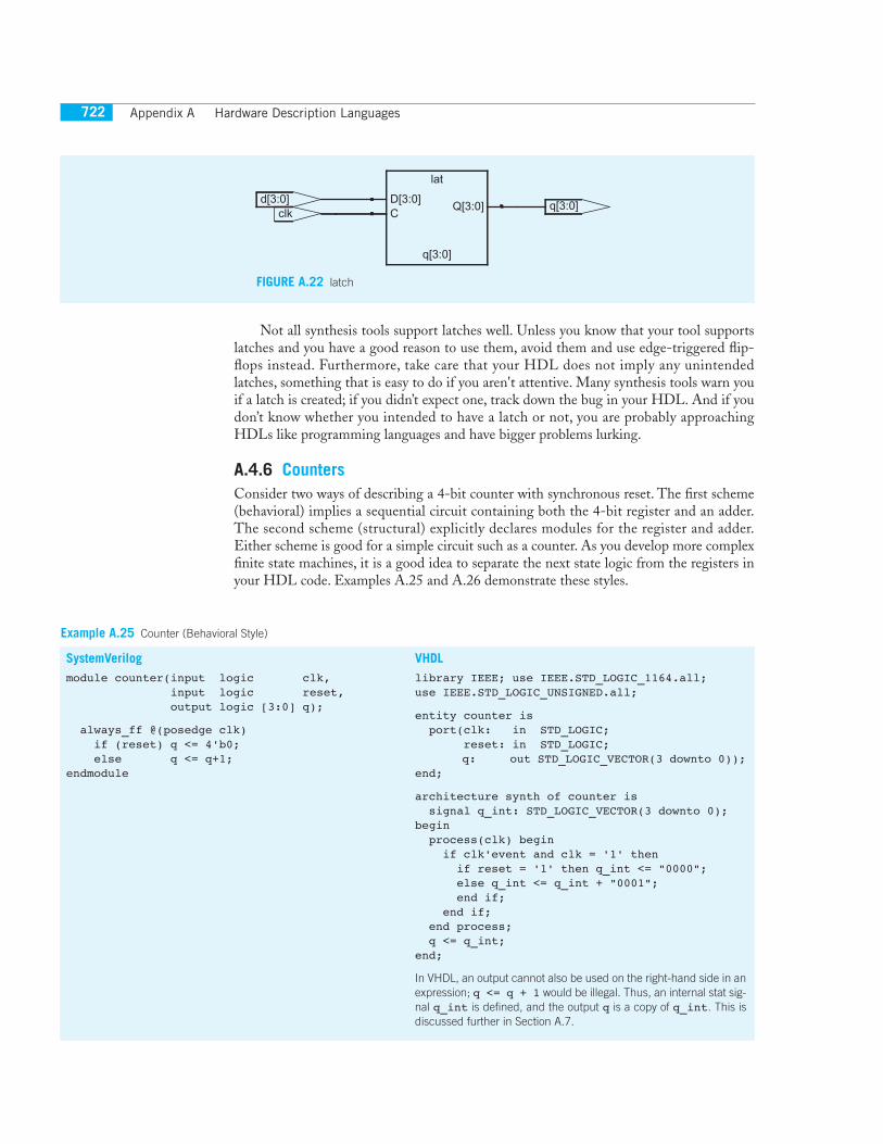
A.4.6 CountersConsider two ways of describing a 4-bit counter with synchronous reset. The first scheme(behavioral) implies a sequential circuit containing both the 4-bit register and an adder.The second scheme (structural) explicitly declares modules for the register and adder.Either scheme is good for a simple circuit such as a counter. As you develop more complexfinite state machines, it is a good idea to separate the next state logic from the registers inyour HDL code. Examples A.25 and A.26 demonstrate these styles.
lat
q[3:0]
q[3:0]d[3:0]
clkD[3:0]
Q[3:0]C
FIGURE A.22 latch
SystemVerilog
module counter(input logic clk, input logic reset, output logic [3:0] q);
always_ff @(posedge clk) if (reset) q <= 4'b0; else q <= q+1;endmodule
VHDL
library IEEE; use IEEE.STD_LOGIC_1164.all;use IEEE.STD_LOGIC_UNSIGNED.all;
entity counter is port(clk: in STD_LOGIC; reset: in STD_LOGIC; q: out STD_LOGIC_VECTOR(3 downto 0));end;
architecture synth of counter is signal q_int: STD_LOGIC_VECTOR(3 downto 0);begin process(clk) begin if clk'event and clk = '1' then if reset = '1' then q_int <= "0000"; else q_int <= q_int + "0001"; end if; end if; end process; q <= q_int;end;
In VHDL, an output cannot also be used on the right-hand side in anexpression; q <= q + 1 would be illegal. Thus, an internal stat sig-nal q_int is defined, and the output q is a copy of q_int. This isdiscussed further in Section A.7.
Example A.25 Counter (Behavioral Style)
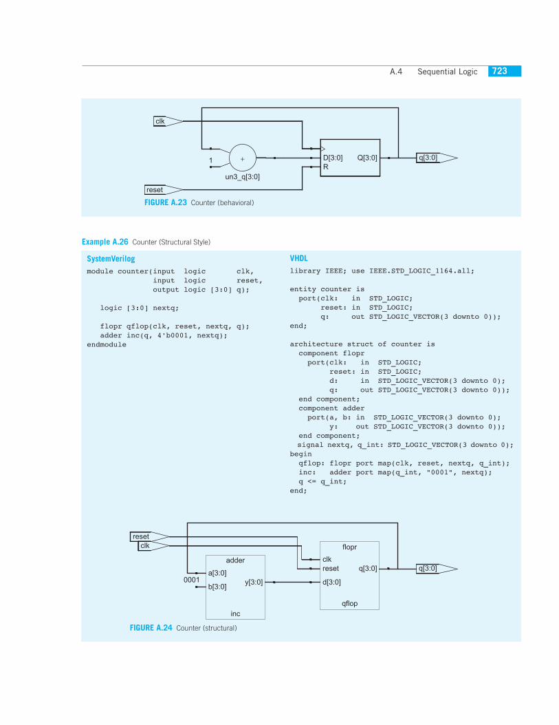
A.4 Sequential Logic 723
un3_q[3:0]
+ q[3:0]
reset
clk
1 Q[3:0]D[3:0]R
FIGURE A.23 Counter (behavioral)
Example A.26 Counter (Structural Style)
SystemVerilog
module counter(input logic clk, input logic reset, output logic [3:0] q);
logic [3:0] nextq;
flopr qflop(clk, reset, nextq, q); adder inc(q, 4'b0001, nextq); endmodule
VHDL
library IEEE; use IEEE.STD_LOGIC_1164.all;
entity counter is port(clk: in STD_LOGIC; reset: in STD_LOGIC; q: out STD_LOGIC_VECTOR(3 downto 0));end;
architecture struct of counter is component flopr port(clk: in STD_LOGIC; reset: in STD_LOGIC; d: in STD_LOGIC_VECTOR(3 downto 0); q: out STD_LOGIC_VECTOR(3 downto 0)); end component; component adder port(a, b: in STD_LOGIC_VECTOR(3 downto 0); y: out STD_LOGIC_VECTOR(3 downto 0)); end component; signal nextq, q_int: STD_LOGIC_VECTOR(3 downto 0);begin qflop: flopr port map(clk, reset, nextq, q_int); inc: adder port map(q_int, "0001", nextq); q <= q_int;end;
flopr
qflop
adder
inc
q[3:0]
resetclk
clkreset
d[3:0]
q[3:0]a[3:0]
0001b[3:0]
y[3:0]
FIGURE A.24 Counter (structural)
Appendix A Hardware Description Languages724
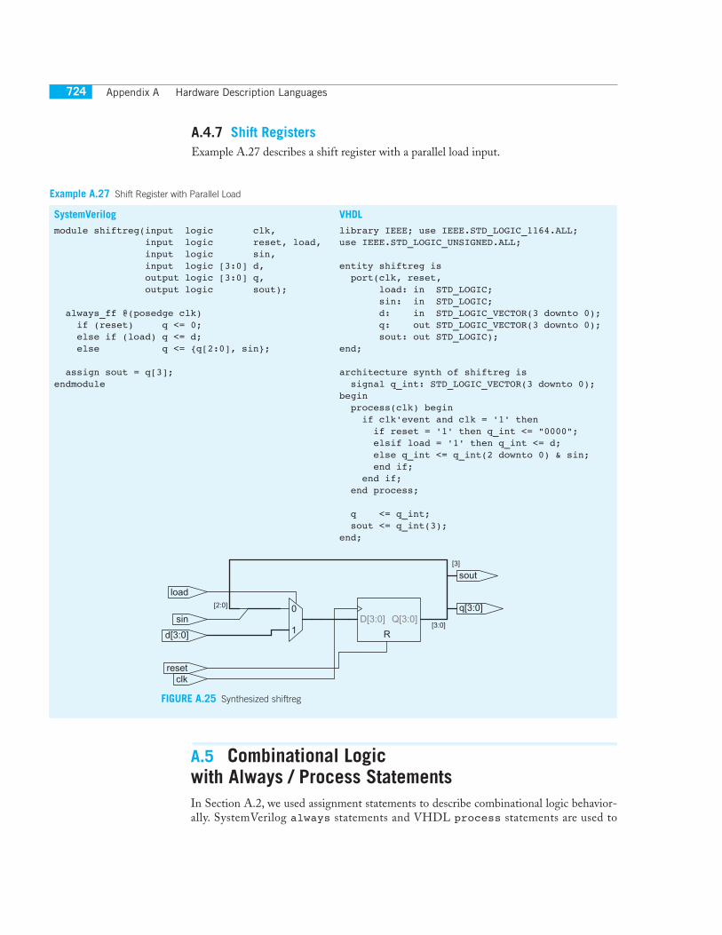
A.4.7 Shift RegistersExample A.27 describes a shift register with a parallel load input.
SystemVerilog
module shiftreg(input logic clk, input logic reset, load, input logic sin, input logic [3:0] d, output logic [3:0] q, output logic sout);
always_ff @(posedge clk) if (reset) q <= 0; else if (load) q <= d; else q <= {q[2:0], sin};
assign sout = q[3];endmodule
VHDL
library IEEE; use IEEE.STD_LOGIC_1164.ALL;use IEEE.STD_LOGIC_UNSIGNED.ALL;
entity shiftreg is port(clk, reset, load: in STD_LOGIC; sin: in STD_LOGIC; d: in STD_LOGIC_VECTOR(3 downto 0); q: out STD_LOGIC_VECTOR(3 downto 0); sout: out STD_LOGIC);end;
architecture synth of shiftreg is signal q_int: STD_LOGIC_VECTOR(3 downto 0);begin process(clk) begin if clk'event and clk = '1' then if reset = '1' then q_int <= "0000"; elsif load = '1' then q_int <= d; else q_int <= q_int(2 downto 0) & sin; end if; end if; end process;
q <= q_int; sout <= q_int(3);end;
Example A.27 Shift Register with Parallel Load
0
1 R
sout
q[3:0]
d[3:0]
sin
load
resetclk
[2:0]
[3:0]Q[3:0]D[3:0]
[3]
FIGURE A.25 Synthesized shiftreg
A.5 Combinational Logic with Always / Process StatementsIn Section A.2, we used assignment statements to describe combinational logic behavior-ally. SystemVerilog always statements and VHDL process statements are used to
A.5 Combinational Logic with Always / Process Statements 725
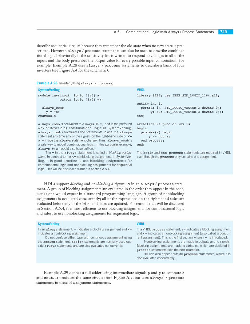
describe sequential circuits because they remember the old state when no new state is pre-scribed. However, always / process statements can also be used to describe combina-tional logic behaviorally if the sensitivity list is written to respond to changes in all of theinputs and the body prescribes the output value for every possible input combination. Forexample, Example A.28 uses always / process statements to describe a bank of fourinverters (see Figure A.4 for the schematic).
SystemVerilog
module inv(input logic [3:0] a, output logic [3:0] y);
always_comb y = ~a;endmodule
always_comb is equivalent to always @(*) and is the preferredway of descr ibing combinat ional logic in SystemVeri log.always_comb reevaluates the statements inside the alwaysstatement any time any of the signals on the right-hand side of <=or = inside the always statement change. Thus, always_comb isa safe way to model combinational logic. In this particular example,always @(a) would also have sufficed.
The = in the always statement is called a blocking assign-ment, in contrast to the <= nonblocking assignment. In SystemVer-i log, i t is good pract ice to use blocking assignments forcombinational logic and nonblocking assignments for sequentiallogic. This will be discussed further in Section A.5.4.
VHDL
library IEEE; use IEEE.STD_LOGIC_1164.all;
entity inv is port(a: in STD_LOGIC_VECTOR(3 downto 0); y: out STD_LOGIC_VECTOR(3 downto 0));end;
architecture proc of inv isbegin process(a) begin y <= not a; end process;end;
The begin and end process statements are required in VHDLeven though the process only contains one assignment.
Example A.28 Inverter (Using always / process)
HDLs support blocking and nonblocking assignments in an always / process state-ment. A group of blocking assignments are evaluated in the order they appear in the code,just as one would expect in a standard programming language. A group of nonblockingassignments is evaluated concurrently; all of the expressions on the right-hand sides areevaluated before any of the left-hand sides are updated. For reasons that will be discussedin Section A.5.4, it is most efficient to use blocking assignments for combinational logicand safest to use nonblocking assignments for sequential logic.
SystemVerilog
In an always statement, = indicates a blocking assignment and <=indicates a nonblocking assignment.
Do not confuse either type with continuous assignment usingthe assign statement. assign statements are normally used out-side always statements and are also evaluated concurrently.
VHDL
In a VHDL process statement, := indicates a blocking assignmentand <= indicates a nonblocking assignment (also called a concur-rent assignment). This is the first section where := is introduced.
Nonblocking assignments are made to outputs and to signals.Blocking assignments are made to variables, which are declared inprocess statements (see the next example).
<= can also appear outside process statements, where it isalso evaluated concurrently.
Example A.29 defines a full adder using intermediate signals p and g to compute sand cout. It produces the same circuit from Figure A.9, but uses always / processstatements in place of assignment statements.
Appendix A Hardware Description Languages726
These two examples are poor applications of always / process statements formodeling combinational logic because they require more lines than the equivalentapproach with assign statements from Section A.2.1. Moreover, they pose the risk ofinadvertently implying sequential logic if the sensitivity list leaves out inputs. However,case and if statements are convenient for modeling more complicated combinationallogic. case and if statements can only appear within always / process statements.
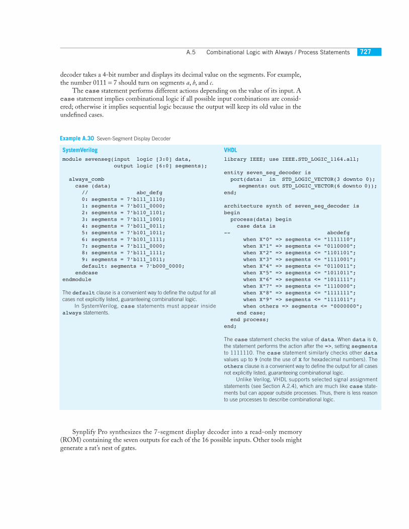
A.5.1 Case StatementsA better application of using the always / process statement for combinational logic isa 7-segment display decoder that takes advantage of the case statement, which mustappear inside an always / process statement.
The design process for describing large blocks of combinational logic with Booleanequations is tedious and prone to error. HDLs offer a great improvement, allowing you tospecify the function at a higher level of abstraction, then automatically synthesize thefunction into gates. Example A.30 uses case statements to describe a 7-segment displaydecoder based on its truth table. A 7-segment display is shown in Figure A.26. The
SystemVerilog
module fulladder(input logic a, b, cin, output logic s, cout);
logic p, g;
always_comb begin p = a ^ b; // blocking g = a & b; // blocking
s = p ^ cin; cout = g | (p & cin); endendmodule
In this case, always @(a, b, cin) or always @(*) wouldhave been equivalent to always_comb. All three reevaluate thecontents of the always block any time a, b, or cin change. How-ever, always_comb is preferred because it is succinct and allowsSystemVerilog tools to generate a warning if the block inadvertentlydescribes sequential logic.
Notice that the begin / end construct is necessarybecause multiple statements appear in the always statement. Thisis analogous to { } in C or Java. The begin / end was notneeded in the flopr example because if / else counts as asingle statement.
This example uses blocking assignments, first computing p,then g, then s, and finally cout.
VHDL
library IEEE; use IEEE.STD_LOGIC_1164.all;
entity fulladder is port(a, b, cin: in STD_LOGIC; s, cout: out STD_LOGIC);end;
architecture synth of fulladder isbegin process (a, b, cin) variable p, g: STD_LOGIC; begin p := a xor b; -- blocking g := a and b; -- blocking
s <= p xor cin; cout <= g or (p and cin); end process;end;
The process sensitivity list must include a, b, and cin becausecombinational logic should respond to changes of any input. If anyof these inputs were omitted, the code might synthesize to sequen-tial logic or might behave differently in simulation and synthesis.
This example uses blocking assignments for p and g so thatthey get their new values before being used to compute s andcout that depend on them.
Because p and g appear on the left-hand side of a blockingassignment (:=) in a process statement, they must be declared tobe variable rather than signal. The variable declarationappears before the begin in the process where the variable isused.
Example A.29 Full Adder (Using always / process)
a
b
c
d
e
f
g
FIGURE A.26 7-segment display
A.5 Combinational Logic with Always / Process Statements 727
decoder takes a 4-bit number and displays its decimal value on the segments. For example,the number 0111 = 7 should turn on segments a, b, and c.
The case statement performs different actions depending on the value of its input. Acase statement implies combinational logic if all possible input combinations are consid-ered; otherwise it implies sequential logic because the output will keep its old value in theundefined cases.
SystemVerilog
module sevenseg(input logic [3:0] data, output logic [6:0] segments);
always_comb case (data) // abc_defg 0: segments = 7'b111_1110; 1: segments = 7'b011_0000; 2: segments = 7'b110_1101; 3: segments = 7'b111_1001; 4: segments = 7'b011_0011; 5: segments = 7'b101_1011; 6: segments = 7'b101_1111; 7: segments = 7'b111_0000; 8: segments = 7'b111_1111; 9: segments = 7'b111_1011; default: segments = 7'b000_0000; endcaseendmodule
The default clause is a convenient way to define the output for allcases not explicitly listed, guaranteeing combinational logic.
In SystemVerilog, case statements must appear insidealways statements.
VHDL
library IEEE; use IEEE.STD_LOGIC_1164.all;
entity seven_seg_decoder is port(data: in STD_LOGIC_VECTOR(3 downto 0); segments: out STD_LOGIC_VECTOR(6 downto 0));end;
architecture synth of seven_seg_decoder isbegin process(data) begin case data is-- abcdefg when X"0" => segments <= "1111110"; when X"1" => segments <= "0110000"; when X"2" => segments <= "1101101"; when X"3" => segments <= "1111001"; when X"4" => segments <= "0110011"; when X"5" => segments <= "1011011"; when X"6" => segments <= "1011111"; when X"7" => segments <= "1110000"; when X"8" => segments <= "1111111"; when X"9" => segments <= "1111011"; when others => segments <= "0000000"; end case; end process;end;
The case statement checks the value of data. When data is 0,the statement performs the action after the =>, setting segmentsto 1111110. The case statement similarly checks other datavalues up to 9 (note the use of X for hexadecimal numbers). Theothers clause is a convenient way to define the output for all casesnot explicitly listed, guaranteeing combinational logic.
Unlike Verilog, VHDL supports selected signal assignmentstatements (see Section A.2.4), which are much like case state-ments but can appear outside processes. Thus, there is less reasonto use processes to describe combinational logic.
Example A.30 Seven-Segment Display Decoder
Synplify Pro synthesizes the 7-segment display decoder into a read-only memory(ROM) containing the seven outputs for each of the 16 possible inputs. Other tools mightgenerate a rat’s nest of gates.
Appendix A Hardware Description Languages728
If the default or others clause were left out of the case statement, the decoderwould have remembered its previous output whenever data were in the range of 10–15.This is strange behavior for hardware, and is not combinational logic.
Ordinary decoders are also commonly written with case statements. Example A.31describes a 3:8 decoder.
rom
segments_1[6:0]
segments[6:0]data[3:0] DOUT[6:0]A[3:0]
FIGURE A.27 sevenseg
SystemVerilog
module decoder3_8(input logic [2:0] a, output logic [7:0] y); always_comb case (a) 3'b000: y = 8'b00000001; 3'b001: y = 8'b00000010; 3'b010: y = 8'b00000100; 3'b011: y = 8'b00001000; 3'b100: y = 8'b00010000; 3'b101: y = 8'b00100000; 3'b110: y = 8'b01000000; 3'b111: y = 8'b10000000; endcaseendmodule
No default statement is needed because all cases are covered.
VHDL
library IEEE; use IEEE.STD_LOGIC_1164.all;
entity decoder3_8 is port(a: in STD_LOGIC_VECTOR(2 downto 0); y: out STD_LOGIC_VECTOR(7 downto 0));end;
architecture synth of decoder3_8 isbegin process(a) begin case a is when "000" => y <= "00000001"; when "001" => y <= "00000010"; when "010" => y <= "00000100"; when "011" => y <= "00001000"; when "100" => y <= "00010000"; when "101" => y <= "00100000"; when "110" => y <= "01000000"; when "111" => y <= "10000000"; when others => y <= (OTHERS => 'X'); end case; end process;end;
Some VHDL tools require an others clause because combinationssuch as "1zx" are not covered. y <= (OTHERS => 'X') sets allthe bits of y to X; this is an unrelated use of the keyword OTHERS.
Example A.31 3:8 Decoder
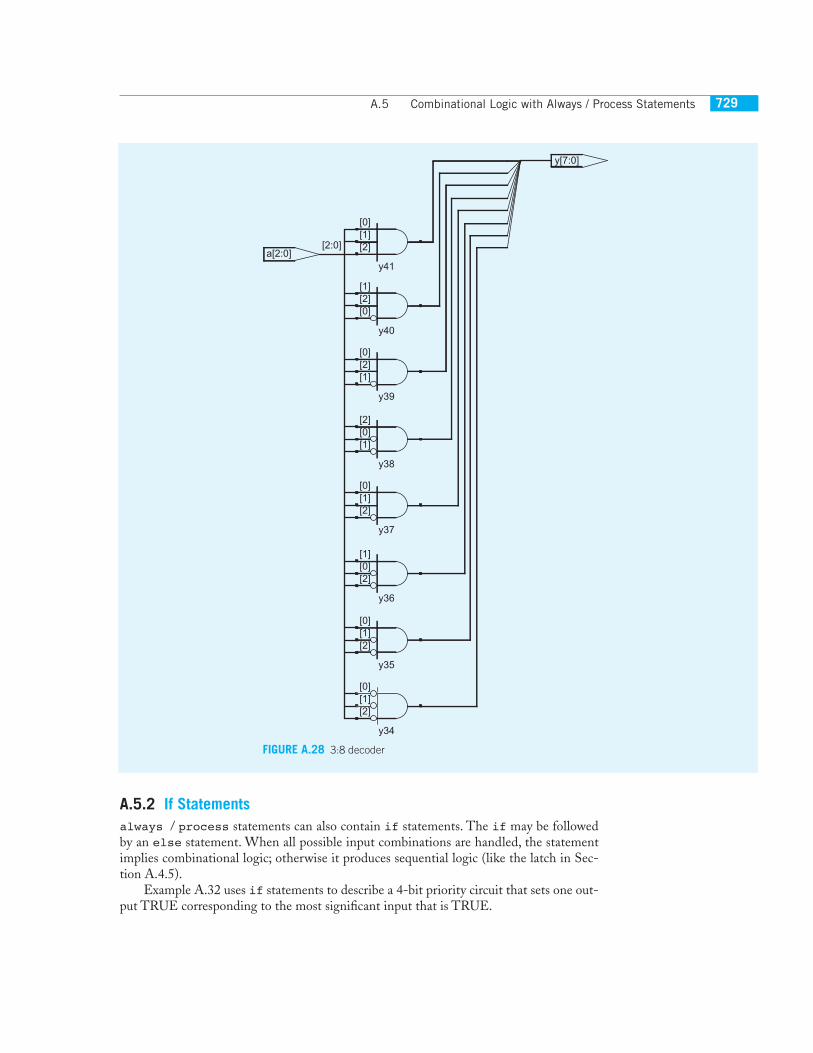
A.5 Combinational Logic with Always / Process Statements 729
A.5.2 If Statementsalways / process statements can also contain if statements. The if may be followedby an else statement. When all possible input combinations are handled, the statementimplies combinational logic; otherwise it produces sequential logic (like the latch in Sec-tion A.4.5).
Example A.32 uses if statements to describe a 4-bit priority circuit that sets one out-put TRUE corresponding to the most significant input that is TRUE.
y41
y34
y35
y36
y37
y38
y39
y40
y[7:0]
a[2:0][2:0]
[0][1][2]
[0][1][2]
[0][1][2]
[1][0][2]
[0][1][2]
[2][0][1]
[0][2][1]
[1][2][0]
FIGURE A.28 3:8 decoder
Appendix A Hardware Description Languages730
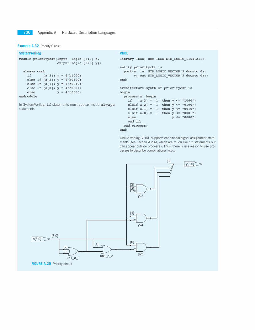
SystemVerilog
module priorityckt(input logic [3:0] a, output logic [3:0] y);
always_comb if (a[3]) y = 4'b1000; else if (a[2]) y = 4'b0100; else if (a[1]) y = 4'b0010; else if (a[0]) y = 4'b0001; else y = 4'b0000;endmodule
In SystemVerilog, if statements must appear inside alwaysstatements.
VHDL
library IEEE; use IEEE.STD_LOGIC_1164.all;
entity priorityckt is port(a: in STD_LOGIC_VECTOR(3 downto 0); y: out STD_LOGIC_VECTOR(3 downto 0));end;
architecture synth of priorityckt isbegin process(a) begin if a(3) = '1' then y <= "1000"; elsif a(2) = '1' then y <= "0100"; elsif a(1) = '1' then y <= "0010"; elsif a(0) = '1' then y <= "0001"; else y <= "0000"; end if; end process;end;
Unlike Verilog, VHDL supports conditional signal assignment state-ments (see Section A.2.4), which are much like if statements butcan appear outside processes. Thus, there is less reason to use pro-cesses to describe combinational logic.
Example A.32 Priority Circuit
un1_a_1
y23
un1_a_3
y24
y25
y[3:0]
a[3:0][3:0]
[3]
[2][3]
[2][3]
[1]
[1]
[0]
FIGURE A.29 Priority circuit
A.5 Combinational Logic with Always / Process Statements 731
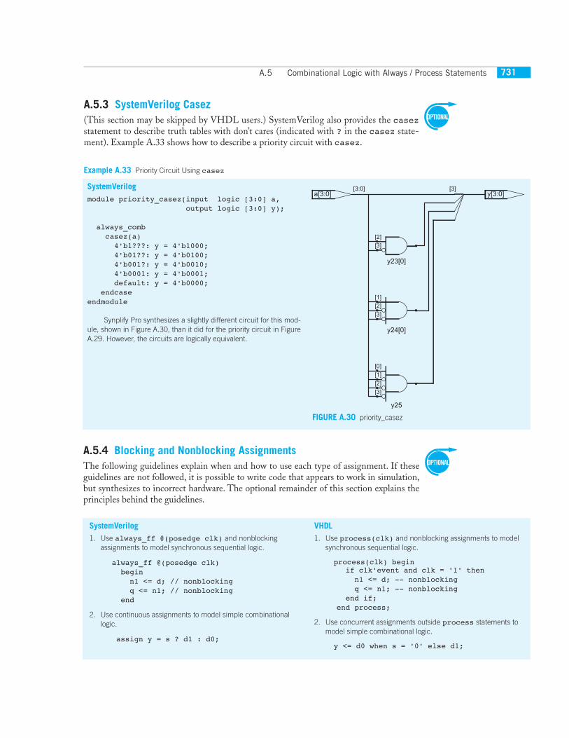
A.5.3 SystemVerilog Casez(This section may be skipped by VHDL users.) SystemVerilog also provides the casezstatement to describe truth tables with don’t cares (indicated with ? in the casez state-ment). Example A.33 shows how to describe a priority circuit with casez.
SystemVerilog
module priority_casez(input logic [3:0] a, output logic [3:0] y);
always_comb casez(a) 4'b1???: y = 4'b1000; 4'b01??: y = 4'b0100; 4'b001?: y = 4'b0010; 4'b0001: y = 4'b0001; default: y = 4'b0000; endcaseendmodule
Synplify Pro synthesizes a slightly different circuit for this mod-ule, shown in Figure A.30, than it did for the priority circuit in FigureA.29. However, the circuits are logically equivalent.
Example A.33 Priority Circuit Using casez
y23[0]
y24[0]
y25
y[3:0]a[3:0][3:0] [3]
[2]
[3]
[1]
[2]
[3]
[0]
[1]
[2]
[3]
FIGURE A.30 priority_casez
A.5.4 Blocking and Nonblocking AssignmentsThe following guidelines explain when and how to use each type of assignment. If theseguidelines are not followed, it is possible to write code that appears to work in simulation,but synthesizes to incorrect hardware. The optional remainder of this section explains theprinciples behind the guidelines.
VHDL
1. Use process(clk) and nonblocking assignments to model synchronous sequential logic.
process(clk) begin if clk'event and clk = '1' then n1 <= d; -- nonblocking q <= n1; -- nonblocking end if; end process;
2. Use concurrent assignments outside process statements to model simple combinational logic.
y <= d0 when s = '0' else d1;
SystemVerilog
1. Use always_ff @(posedge clk) and nonblocking assignments to model synchronous sequential logic.
always_ff @(posedge clk) begin n1 <= d; // nonblocking q <= n1; // nonblocking end
2. Use continuous assignments to model simple combinational logic.
assign y = s ? d1 : d0;

Appendix A Hardware Description Languages732
A.5.4.1 Combinational LogicThe full adder from Example A.29 is correctly modeled using blocking assignments. Thissection explores how it operates and how it would differ if nonblocking assignments hadbeen used.
Imagine that a, b, and cin are all initially 0. p, g, s, and cout are thus 0 as well. Atsome time, a changes to 1, triggering the always / process statement. The four block-ing assignments evaluate in the order shown below. Note that p and g get their new valuebefore s and cout are computed because of the blocking assignments. This is importantbecause we want to compute s and cout using the new values of p and g.
Example A.34 illustrates the use of nonblocking assignments (not recommended).
1 1 0 12 1 0 03 1 0 14 0 1 0 0
.. ·.. ·
p
g
s
cout
← ⊕ =← =← ⊕ =
← + =
SystemVerilog (continued) 3. Use always_comb and blocking assignments to model more
complicated combinational logic where the always statement ishelpful.
always_comb begin p = a ^ b; // blocking g = a & b; // blocking s = p ^ cin; cout = g | (p & cin); end
4. Do not make assignments to the same signal in more than onealways statement or continuous assignment statement. Excep-tion: tristate busses.
VHDL (continued) 3. Use process(in1, in2, ...) to model more compli-
cated combinational logic where the process is helpful.Use blocking assignments to internal variables.
process(a, b, cin) variable p, g: STD_LOGIC; begin p := a xor b; -- blocking g := a and b; -- blocking s <= p xor cin; cout <= g or (p and cin); end process;
4. Do not make assignments to the same variable in morethan one process or concurrent assignment statement.Exception: tristate busses.
Example A.34 Full Adder Using Nonblocking Assignments
SystemVerilog
// nonblocking assignments (not recommended)module fulladder(input logic a, b, cin, output logic s, cout);
logic p, g;
always_comb begin p <= a ^ b; // nonblocking g <= a & b; // nonblocking
s <= p ^ cin; cout <= g | (p & cin); endendmodule
VHDL
-- nonblocking assignments (not recommended)library IEEE; use IEEE.STD_LOGIC_1164.all;
entity fulladder is port(a, b, cin: in STD_LOGIC; s, cout: out STD_LOGIC);end;
architecture nonblocking of fulladder is signal p, g: STD_LOGIC;begin process (a, b, cin, p, g) begin p <= a xor b; -- nonblocking g <= a and b; -- nonblocking
A.5 Combinational Logic with Always / Process Statements 733
Consider the same case of a rising from 0 to 1 while b and cin are 0. The four non-blocking assignments evaluate concurrently as follows:
Observe that s is computed concurrently with p and hence uses the old value of p, notthe new value. Hence, s remains 0 rather than becoming 1. However, p does change from0 to 1. This change triggers the always / process statement to evaluate a second time asfollows:
This time, p was already 1, so s correctly changes to 1. The nonblocking assignmentseventually reached the right answer, but the always / process statement had to evalu-ate twice. This makes simulation more time consuming, although it synthesizes to thesame hardware.
Another drawback of nonblocking assignments in modeling combinational logic isthat the HDL will produce the wrong result if you forget to include the intermediate vari-ables in the sensitivity list, as shown below.
p g s cout← ⊕ = ← = ← ⊕ = ← + =1 0 1 1 0 0 0 0 0 0 0 0 0· ·
p g s cout← ⊕ = ← = ← ⊕ = ← + =1 0 1 1 0 0 0 0 0 01 1 1· ·
VHDL (continued) s <= p xor cin; cout <= g or (p and cin); end process;end;
Because p and g appear on the left-hand side of a nonblockingassignment in a process statement, they must be declared to besignal rather than variable. The signal declaration appearsbefore the begin in the architecture, not the process.
SystemVerilog
If the sensitivity list of the always statement were written asalways @(a, b, cin) rather than always_comb or always@(*), then the statement would not reevaluate when p or gchange. In the previous example, s would be incorrectly left at 0,not 1.
VHDL
If the sensitivity list of the process were written as process (a,b, cin) rather than always process (a, b, cin, p, g),then the statement would not reevaluate when p or g change. In theprevious example, s would be incorrectly left at 0, not 1.
Worse yet, some synthesis tools will synthesize the correct hardware even when afaulty sensitivity list causes incorrect simulation. This leads to a mismatch between thesimulation results and what the hardware actually does.
A.5.4.2 Sequential LogicThe synchronizer from Example A.23 is correctly modeled using nonblocking assign-ments. On the rising edge of the clock, d is copied to n1 at the same time that n1 is copiedto q, so the code properly describes two registers. For example, suppose initially that d = 0,n1 = 1, and q = 0. On the rising edge of the clock, the following two assignments occurconcurrently, so that after the clock edge, n1 = 0 and q = 1.
n d q n1 0 1 1← = ← =
Appendix A Hardware Description Languages734
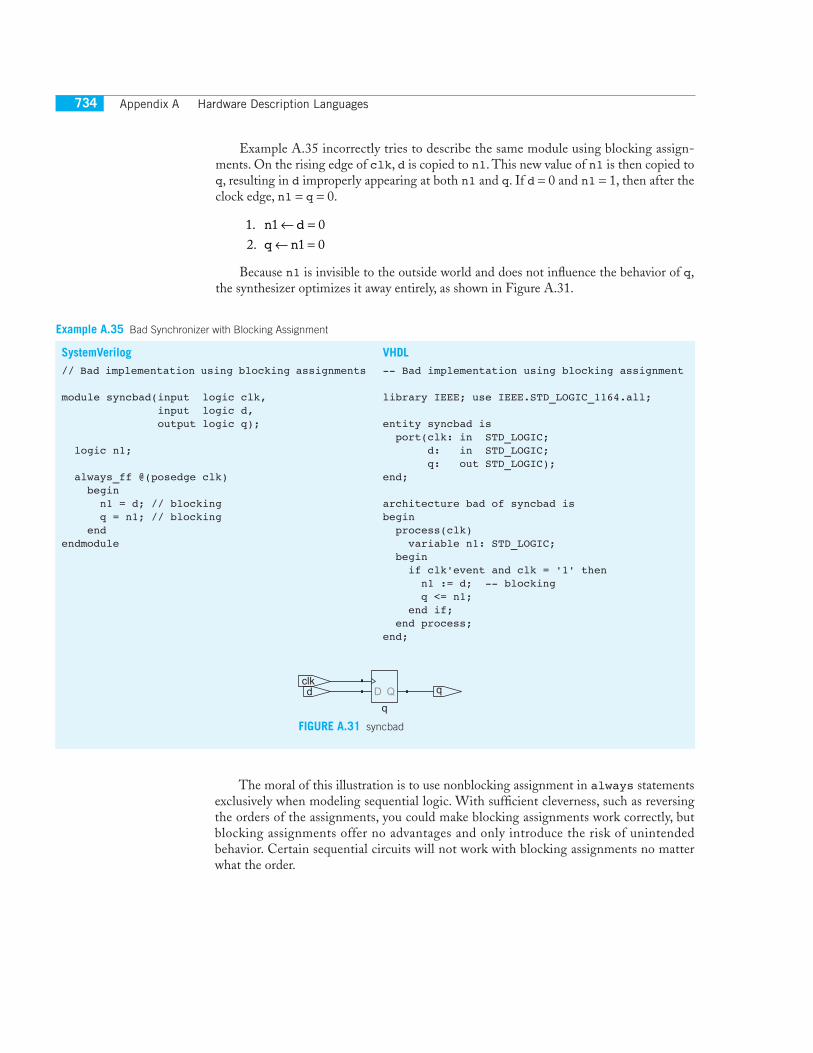
Example A.35 incorrectly tries to describe the same module using blocking assign-ments. On the rising edge of clk, d is copied to n1. This new value of n1 is then copied toq, resulting in d improperly appearing at both n1 and q. If d = 0 and n1 = 1, then after theclock edge, n1 = q = 0.
Because n1 is invisible to the outside world and does not influence the behavior of q,the synthesizer optimizes it away entirely, as shown in Figure A.31.
1 1 02 1 0..n d
q n
← =← =
Example A.35 Bad Synchronizer with Blocking Assignment
SystemVerilog
// Bad implementation using blocking assignments
module syncbad(input logic clk, input logic d, output logic q);
logic n1;
always_ff @(posedge clk) begin n1 = d; // blocking q = n1; // blocking endendmodule
VHDL
-- Bad implementation using blocking assignment
library IEEE; use IEEE.STD_LOGIC_1164.all;
entity syncbad is port(clk: in STD_LOGIC; d: in STD_LOGIC; q: out STD_LOGIC);end;
architecture bad of syncbad isbegin process(clk) variable n1: STD_LOGIC; begin if clk'event and clk = '1' then n1 := d; -- blocking q <= n1; end if; end process;end;
q
qdclk
QD
FIGURE A.31 syncbad
The moral of this illustration is to use nonblocking assignment in always statementsexclusively when modeling sequential logic. With sufficient cleverness, such as reversingthe orders of the assignments, you could make blocking assignments work correctly, butblocking assignments offer no advantages and only introduce the risk of unintendedbehavior. Certain sequential circuits will not work with blocking assignments no matterwhat the order.
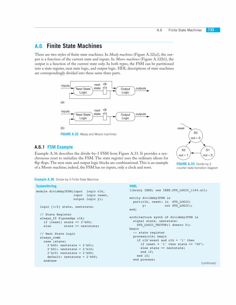
A.6 Finite State Machines 735
A.6 Finite State MachinesThere are two styles of finite state machines. In Mealy machines (Figure A.32(a)), the out-put is a function of the current state and inputs. In Moore machines (Figure A.32(b)), theoutput is a function of the current state only. In both types, the FSM can be partitionedinto a state register, next state logic, and output logic. HDL descriptions of state machinesare correspondingly divided into these same three parts.
clk
Next StateLogic
nextstate
inputsOutputLogic
outputs
(a)
(b)
clk
Next StateLogic
nextstate
inputsOutputLogic
outputs
FIGURE A.32 Mealy and Moore machines
A.6.1 FSM ExampleExample A.36 describes the divide-by-3 FSM from Figure A.33. It provides a syn-chronous reset to initialize the FSM. The state register uses the ordinary idiom forflip-flops. The next state and output logic blocks are combinational. This is an exampleof a Moore machine; indeed, the FSM has no inputs, only a clock and reset.
S0
out = 0
S1
out = 0
S2
out = 1
reset
FIGURE A.33 Divide-by-3 counter state transition diagram
Example A.36 Divide-by-3 Finite State Machine
SystemVerilog
module divideby3FSM(input logic clk, input logic reset, output logic y);
logic [1:0] state, nextstate;
// State Register always_ff @(posedge clk) if (reset) state <= 2'b00; else state <= nextstate;
// Next State Logic always_comb case (state) 2'b00: nextstate = 2'b01; 2'b01: nextstate = 2'b10; 2'b10: nextstate = 2'b00; default: nextstate = 2'b00; endcase
VHDL library IEEE; use IEEE.STD_LOGIC_1164.all;
entity divideby3FSM is port(clk, reset: in STD_LOGIC; y: out STD_LOGIC);end;
architecture synth of divideby3FSM is signal state, nextstate: STD_LOGIC_VECTOR(1 downto 0);begin -- state register process(clk) begin if clk'event and clk = '1' then if reset = '1' then state <= "00"; else state <= nextstate; end if; end if; end process;
(continues)
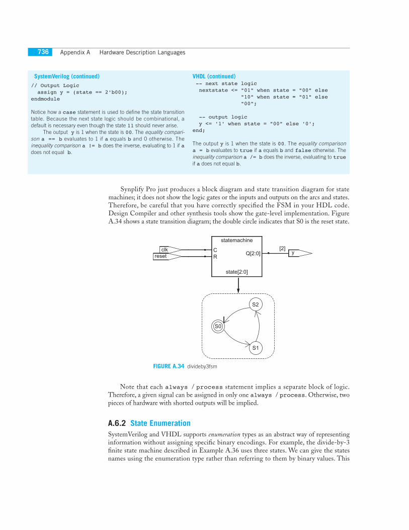
Appendix A Hardware Description Languages736
Synplify Pro just produces a block diagram and state transition diagram for statemachines; it does not show the logic gates or the inputs and outputs on the arcs and states.Therefore, be careful that you have correctly specified the FSM in your HDL code.Design Compiler and other synthesis tools show the gate-level implementation. FigureA.34 shows a state transition diagram; the double circle indicates that S0 is the reset state.
SystemVerilog (continued)// Output Logic assign y = (state == 2'b00);endmodule
Notice how a case statement is used to define the state transitiontable. Because the next state logic should be combinational, adefault is necessary even though the state 11 should never arise.
The output y is 1 when the state is 00. The equality compari-son a == b evaluates to 1 if a equals b and 0 otherwise. Theinequality comparison a != b does the inverse, evaluating to 1 if adoes not equal b.
VHDL (continued) -- next state logic nextstate <= "01" when state = "00" else "10" when state = "01" else "00";
-- output logic y <= '1' when state = "00" else '0';end;
The output y is 1 when the state is 00. The equality comparisona = b evaluates to true if a equals b and false otherwise. Theinequality comparison a /= b does the inverse, evaluating to trueif a does not equal b.
statemachine
state[2:0]
yresetclk C
Q[2:0]R
S0
S1
S2
[2]
FIGURE A.34 divideby3fsm
Note that each always / process statement implies a separate block of logic.Therefore, a given signal can be assigned in only one always / process. Otherwise, twopieces of hardware with shorted outputs will be implied.
A.6.2 State EnumerationSystemVerilog and VHDL supports enumeration types as an abstract way of representinginformation without assigning specific binary encodings. For example, the divide-by-3finite state machine described in Example A.36 uses three states. We can give the statesnames using the enumeration type rather than referring to them by binary values. This
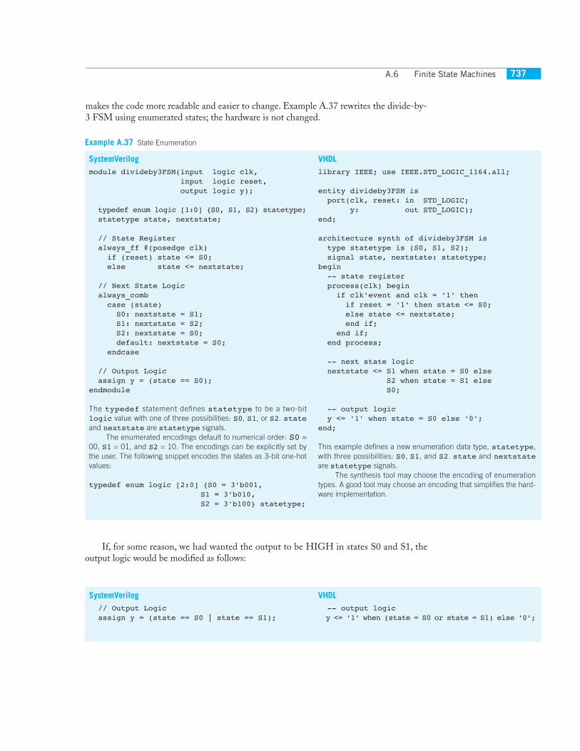
A.6 Finite State Machines 737
makes the code more readable and easier to change. Example A.37 rewrites the divide-by-3 FSM using enumerated states; the hardware is not changed.
Example A.37 State Enumeration
SystemVerilog
module divideby3FSM(input logic clk, input logic reset, output logic y);
typedef enum logic [1:0] {S0, S1, S2} statetype; statetype state, nextstate;
// State Register always_ff @(posedge clk) if (reset) state <= S0; else state <= nextstate;
// Next State Logic always_comb case (state) S0: nextstate = S1; S1: nextstate = S2; S2: nextstate = S0; default: nextstate = S0; endcase
// Output Logic assign y = (state == S0);endmodule
The typedef statement defines statetype to be a two-bitlogic value with one of three possibilities: S0, S1, or S2. stateand nextstate are statetype signals.
The enumerated encodings default to numerical order: S0 =00, S1 = 01, and S2 = 10. The encodings can be explicitly set bythe user. The following snippet encodes the states as 3-bit one-hotvalues:
typedef enum logic [2:0] {S0 = 3'b001,S1 = 3'b010,S2 = 3'b100} statetype;
VHDL
library IEEE; use IEEE.STD_LOGIC_1164.all;
entity divideby3FSM is port(clk, reset: in STD_LOGIC; y: out STD_LOGIC);end;
architecture synth of divideby3FSM is type statetype is (S0, S1, S2); signal state, nextstate: statetype;begin -- state register process(clk) begin if clk'event and clk = '1' then if reset = '1' then state <= S0; else state <= nextstate; end if; end if; end process;
-- next state logic nextstate <= S1 when state = S0 else S2 when state = S1 else S0;
-- output logic y <= '1' when state = S0 else '0';end;
This example defines a new enumeration data type, statetype,with three possibilities: S0, S1, and S2. state and nextstateare statetype signals.
The synthesis tool may choose the encoding of enumerationtypes. A good tool may choose an encoding that simplifies the hard-ware implementation.
If, for some reason, we had wanted the output to be HIGH in states S0 and S1, theoutput logic would be modified as follows:
SystemVerilog
// Output Logic assign y = (state == S0 | state == S1);
VHDL
-- output logic y <= '1' when (state = S0 or state = S1) else '0';
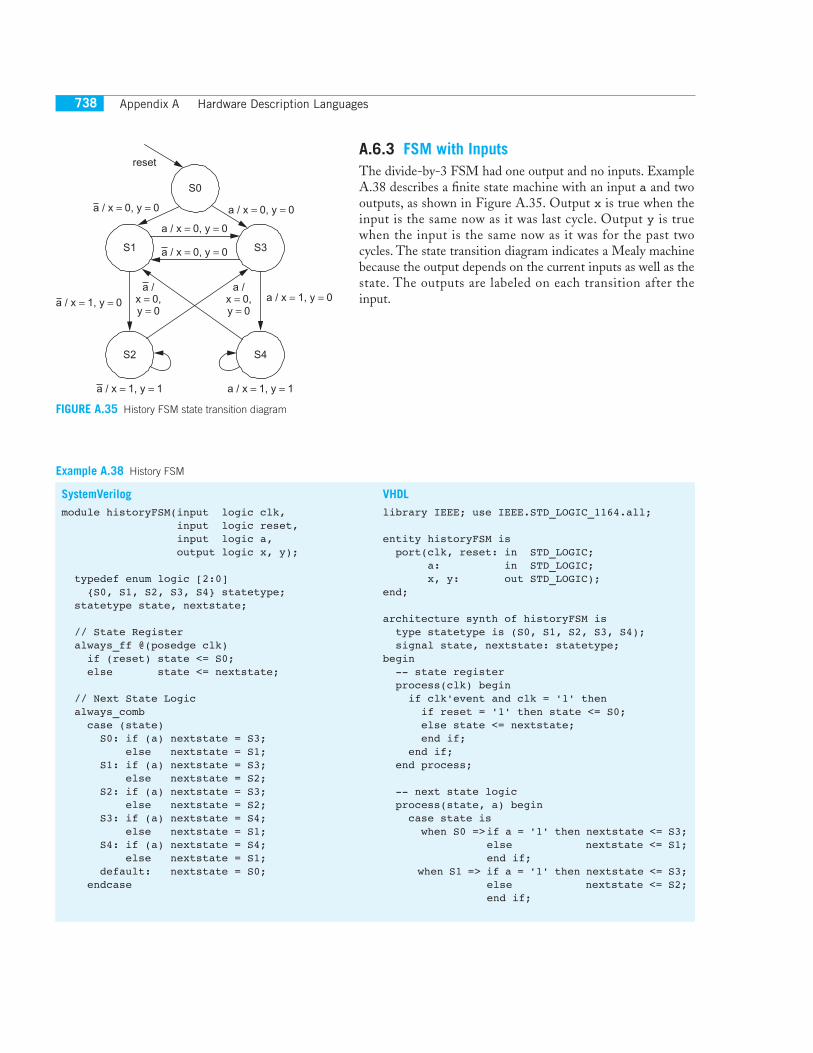
Appendix A Hardware Description Languages738
A.6.3 FSM with InputsThe divide-by-3 FSM had one output and no inputs. ExampleA.38 describes a finite state machine with an input a and twooutputs, as shown in Figure A.35. Output x is true when theinput is the same now as it was last cycle. Output y is truewhen the input is the same now as it was for the past twocycles. The state transition diagram indicates a Mealy machinebecause the output depends on the current inputs as well as thestate. The outputs are labeled on each transition after theinput.
S0
S3S1
reset
S4S2
a / x = 0, y = 0
a / x = 1, y = 0a /
x = 0,y = 0
a / x = 0, y = 0
a / x = 0, y = 0
a / x = 1, y = 0a /
x = 0,y = 0
a / x = 1, y = 1 a / x = 1, y = 1
a / x = 0, y = 0
FIGURE A.35 History FSM state transition diagram
Example A.38 History FSM
SystemVerilog
module historyFSM(input logic clk, input logic reset, input logic a, output logic x, y);
typedef enum logic [2:0] {S0, S1, S2, S3, S4} statetype; statetype state, nextstate;
// State Register always_ff @(posedge clk) if (reset) state <= S0; else state <= nextstate;
// Next State Logic always_comb case (state) S0: if (a) nextstate = S3; else nextstate = S1; S1: if (a) nextstate = S3; else nextstate = S2; S2: if (a) nextstate = S3; else nextstate = S2; S3: if (a) nextstate = S4; else nextstate = S1; S4: if (a) nextstate = S4; else nextstate = S1; default: nextstate = S0; endcase
VHDL
library IEEE; use IEEE.STD_LOGIC_1164.all;
entity historyFSM is port(clk, reset: in STD_LOGIC; a: in STD_LOGIC; x, y: out STD_LOGIC);end;
architecture synth of historyFSM is type statetype is (S0, S1, S2, S3, S4); signal state, nextstate: statetype;begin -- state register process(clk) begin if clk'event and clk = '1' then if reset = '1' then state <= S0; else state <= nextstate; end if; end if; end process;
-- next state logic process(state, a) begin case state is when S0 =>if a = '1' then nextstate <= S3; else nextstate <= S1; end if; when S1 => if a = '1' then nextstate <= S3; else nextstate <= S2; end if;
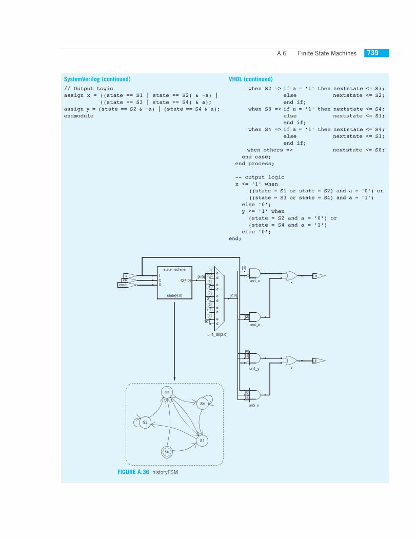
A.6 Finite State Machines 739
SystemVerilog (continued) // Output Logicassign x = ((state == S1 | state == S2) & ~a) | ((state == S3 | state == S4) & a);assign y = (state == S2 & ~a) | (state == S4 & a);endmodule
VHDL (continued) when S2 => if a = '1' then nextstate <= S3;
else nextstate <= S2;end if;
when S3 => if a = '1' then nextstate <= S4;else nextstate <= S1;end if;
when S4 => if a = '1' then nextstate <= S4;else nextstate <= S1;end if;
when others => nextstate <= S0; end case; end process;
-- output logic x <= '1' when
((state = S1 or state = S2) and a = '0') or((state = S3 or state = S4) and a = '1')
else '0'; y <= '1' when (state = S2 and a = '0') or (state = S4 and a = '1') else '0';end;
statemachine
state[4:0]
un1_S0[2:0]
ed
ed
ed
ed
ed
un1_x
un4_x
un1_y
un5_y
x
y
y
xaclk
reset
I [4:0]Q[4:0]C
R
[0]
000
[1]
010
[2][2:0]
011
[3]
100
[4]
101
[1]
[2]
[0][1]
[0][2]
S3
S4
S1
S0
S2
FIGURE A.36 historyFSM
Appendix A Hardware Description Languages740
A.7 Type IdiosyncraciesThis section explains some subtleties about SystemVerilog and VHDL types in moredepth.
SystemVerilog
Standard Verilog primarily uses two types: reg and wire. Despiteits name, a reg signal might or might not be associated with a regis-ter. This was a great source of confusion for those learning the lan-guage. SystemVerilog introduced the logic type and relaxed somerequirements to eliminate the confusion; hence, the examples inthis appendix use logic. This section explains the reg and wiretypes in more detail for those who need to read legacy Verilog code.
In Verilog, if a signal appears on the left-hand side of <= or = inan always block, it must be declared as reg. Otherwise, it shouldbe declared as wire. Hence, a reg signal might be the output of aflip-flop, a latch, or combinational logic, depending on the sensitivitylist and statement of an always block.
Input and output ports default to the wire type unless theirtype is explicitly specified as reg. The following example shows howa flip-flop is described in conventional Verilog. Notice that clk andd default to wire, while q is explicitly defined as reg because itappears on the left-hand side of <= in the always block.
module flop(input clk, input [3:0] d, output reg [3:0] q);
always @(posedge clk) q <= d;endmodule
SystemVerilog introduces the logic type. logic is a syn-onym for reg and avoids misleading users about whether it is actu-ally a flip-flop. Moreover, SystemVerilog relaxes the rules on assignstatements and hierarchical port instantiations so logic can beused outside always blocks where a wire traditionally would berequired. Thus, nearly all SystemVerilog signals can be logic. Theexception is that signals with multiple drivers (e.g., a tristate bus)must be declared as a net, as described in Example A.11. This ruleallows SystemVerilog to generate an error message rather than an xvalue when a logic signal is accidentally connected to multipledrivers.
The most common type of net is called a wire or tri. Thesetwo types are synonymous, but wire is conventionally used when asingle driver is present and tri is used when multiple drivers arepresent. Thus, wire is obsolete in SystemVerilog because logic ispreferred for signals with a single driver.
When a tri net is driven to a single value by one or moredrivers, it takes on that value. When it is undriven, it floats (z). Whenit is driven to different values (0, 1, or x) by multiple drivers, it is incontention (x).
There are other net types that resolve differently whenundriven or driven by multiple sources. The other types are rarely
VHDL
Unlike SystemVerilog, VHDL enforces a strict data typing systemthat can protect the user from some errors but that is also clumsy attimes.
Despite its fundamental importance, the STD_LOGIC type is not built into VHDL. Instead, it is part of the IEEE.STD_LOGIC_1164 library. Thus, every file must contain the library statements we have seen in the previous examples.
Moreover, IEEE.STD_LOGIC_1164 lacks basic operationssuch as addition, comparison, shifts, and conversion to integers forSTD_LOGIC_VECTOR data. Most CAD vendors have adopted yetmore libraries containing these functions:
IEEE.STD_LOGIC_UNSIGNED andIEEE.STD_LOGIC_SIGNED.
VHDL also has a BOOLEAN type with two values: true andfalse. BOOLEAN values are returned by comparisons (like s ='0') and used in conditional statements such as when. Despite thetemptation to believe a BOOLEAN true value should be equivalentto a STD_LOGIC '1' and BOOLEAN false should meanSTD_LOGIC '0', these types are not interchangeable. Thus, thefollowing code is illegal:
y <= d1 when s else d0; q <= (state = S2);
Instead, we must write
y <= d1 when s = '1' else d0; q <= '1' when state = S2 else '0';
While we will not declare any signals to be BOOLEAN, they are auto-matically implied by comparisons and used by conditional state-ments.
Similarly, VHDL has an INTEGER type representing both posi-tive and negative integers. Signals of type INTEGER span at leastthe values –231 … 231-1. Integer values are used as indices of bus-ses. For example, in the statement
y <= a(3) and a(2) and a(1) and a(0);
0, 1, 2, and 3 are integers serving as an index to choose bits of the asignal. We cannot directly index a bus with a STD_LOGIC orSTD_LOGIC_VECTOR signal. Instead, we must convert the signalto an INTEGER. This is demonstrated in Example A.39 for an 8:1multiplexer that selects one bit from a vector using a 3-bit index.The CONV_INTEGER func t i on i s defined in theSTD_LOGIC_UNSIGNED library and performs the conversion fromSTD_LOGIC_VECTOR to integer for positive (unsigned) values.
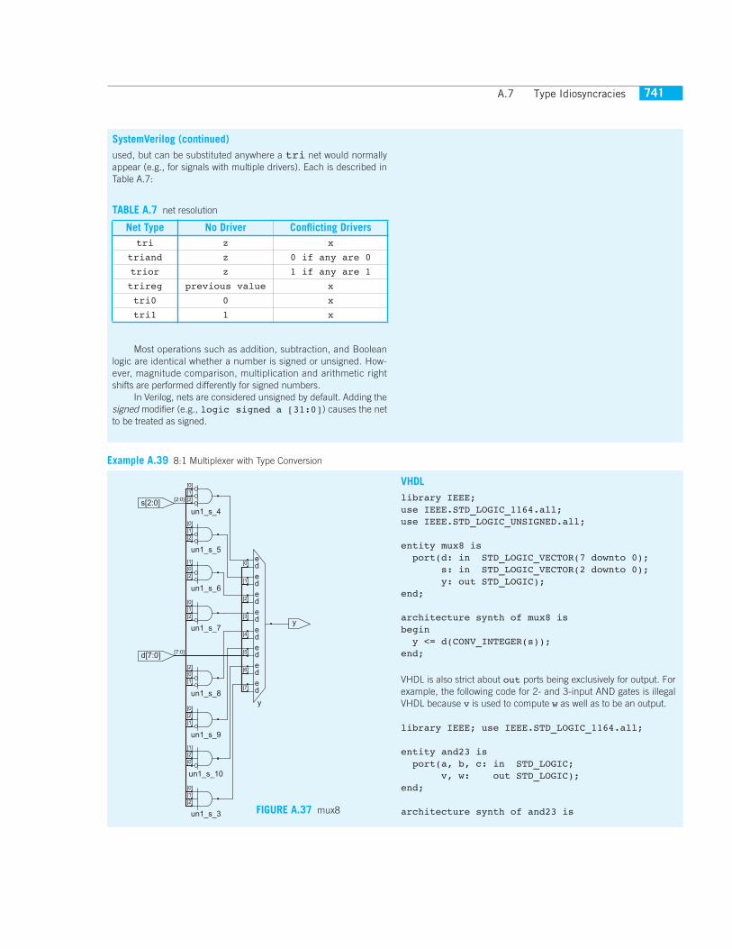
A.7 Type Idiosyncracies 741
SystemVerilog (continued)used, but can be substituted anywhere a tri net would normallyappear (e.g., for signals with multiple drivers). Each is described inTable A.7:
Most operations such as addition, subtraction, and Booleanlogic are identical whether a number is signed or unsigned. How-ever, magnitude comparison, multiplication and arithmetic rightshifts are performed differently for signed numbers.
In Verilog, nets are considered unsigned by default. Adding thesigned modifier (e.g., logic signed a [31:0]) causes the netto be treated as signed.
TABLE A.7 net resolution
Net Type No Driver Conflicting Driverstri z x
triand z 0 if any are 0
trior z 1 if any are 1
trireg previous value x
tri0 0 x
tri1 1 x
Example A.39 8:1 Multiplexer with Type Conversion
VHDL
library IEEE; use IEEE.STD_LOGIC_1164.all; use IEEE.STD_LOGIC_UNSIGNED.all;
entity mux8 is port(d: in STD_LOGIC_VECTOR(7 downto 0); s: in STD_LOGIC_VECTOR(2 downto 0); y: out STD_LOGIC);end;
architecture synth of mux8 isbegin y <= d(CONV_INTEGER(s));end;
VHDL is also strict about out ports being exclusively for output. Forexample, the following code for 2- and 3-input AND gates is illegalVHDL because v is used to compute w as well as to be an output.
library IEEE; use IEEE.STD_LOGIC_1164.all;
entity and23 is port(a, b, c: in STD_LOGIC; v, w: out STD_LOGIC);end;
architecture synth of and23 isun1_s_3
un1_s_4
un1_s_5
un1_s_6
un1_s_7
un1_s_8
un1_s_9
un1_s_10
y
edededededededed
s[2:0] [2:0]
d[7:0]
y
[7:0]
[0][1][2]
[0][1][2]
[0][1][2]
[1][0][2]
[0][1][2]
[2][0][1]
[0][2][1]
[1][2][0]
[0]
[1]
[2]
[3]
[4]
[5]
[6]
[7]
FIGURE A.37 mux8
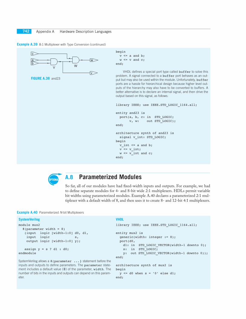
Appendix A Hardware Description Languages742
A.8 Parameterized ModulesSo far, all of our modules have had fixed-width inputs and outputs. For example, we hadto define separate modules for 4- and 8-bit wide 2:1 multiplexers. HDLs permit variablebit widths using parameterized modules. Example A.40 declares a parameterized 2:1 mul-tiplexer with a default width of 8, and then uses it to create 8- and 12-bit 4:1 multiplexers.
Example A.39 8:1 Multiplexer with Type Conversion (continued)
begin v <= a and b; w <= v and c;end;
VHDL defines a special port type called buffer to solve thisproblem. A signal connected to a buffer port behaves as an out-put but may also be used within the module. Unfortunately, bufferports are a hassle for hierarchical design because higher level out-puts of the hierarchy may also have to be converted to buffers. Abetter alternative is to declare an internal signal, and then drive theoutput based on this signal, as follows:
library IEEE; use IEEE.STD_LOGIC_1164.all;
entity and23 is port(a, b, c: in STD_LOGIC; v, w: out STD_LOGIC);end;
architecture synth of and23 is signal v_int: STD_LOGIC;begin v_int <= a and b; v <= v_int; w <= v_int and c;end;
Example A.40 Parameterized N-bit Multiplexers
SystemVerilog
module mux2 #(parameter width = 8) (input logic [width-1:0] d0, d1, input logic s, output logic [width-1:0] y);
assign y = s ? d1 : d0; endmodule
SystemVerilog allows a #(parameter ...) statement before theinputs and outputs to define parameters. The parameter state-ment includes a default value (8) of the parameter, width. Thenumber of bits in the inputs and outputs can depend on this param-eter.
VHDL
library IEEE; use IEEE.STD_LOGIC_1164.all;
entity mux2 is generic(width: integer := 8); port(d0,
d1: in STD_LOGIC_VECTOR(width-1 downto 0);s: in STD_LOGIC;y: out STD_LOGIC_VECTOR(width-1 downto 0));
end;
architecture synth of mux2 isbegin y <= d0 when s = '0' else d1;end;
V W
w
v
c
ba
FIGURE A.38 and23
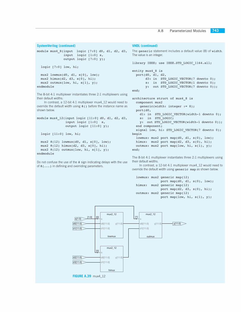
A.8 Parameterized Modules 743
SystemVerilog (continued) module mux4_8(input logic [7:0] d0, d1, d2, d3, input logic [1:0] s, output logic [7:0] y);
logic [7:0] low, hi;
mux2 lowmux(d0, d1, s[0], low); mux2 himux(d2, d3, s[0], hi); mux2 outmux(low, hi, s[1], y);endmodule
The 8-bit 4:1 multiplexer instantiates three 2:1 multiplexers usingtheir default widths.
In contrast, a 12-bit 4:1 multiplexer mux4_12 would need tooverride the default width using #() before the instance name asshown below.
module mux4_12(input logic [11:0] d0, d1, d2, d3, input logic [1:0] s, output logic [11:0] y);
logic [11:0] low, hi;
mux2 #(12) lowmux(d0, d1, s[0], low); mux2 #(12) himux(d2, d3, s[0], hi); mux2 #(12) outmux(low, hi, s[1], y);endmodule
Do not confuse the use of the # sign indicating delays with the useof #(...) in defining and overriding parameters.
VHDL (continued) The generic statement includes a default value (8) of width.The value is an integer.
library IEEE; use IEEE.STD_LOGIC_1164.all;
entity mux4_8 is port(d0, d1, d2, d3: in STD_LOGIC_VECTOR(7 downto 0); s: in STD_LOGIC_VECTOR(1 downto 0); y: out STD_LOGIC_VECTOR(7 downto 0));end;
architecture struct of mux4_8 is component mux2 generic(width: integer := 8); port(d0,
d1: in STD_LOGIC_VECTOR(width-1 downto 0);s: in STD_LOGIC;y: out STD_LOGIC_VECTOR(width-1 downto 0));
end component; signal low, hi: STD_LOGIC_VECTOR(7 downto 0);begin lowmux: mux2 port map(d0, d1, s(0), low); himux: mux2 port map(d2, d3, s(0), hi); outmux: mux2 port map(low, hi, s(1), y);end;
The 8-bit 4:1 multiplexer instantiates three 2:1 multiplexers usingtheir default widths.
In contrast, a 12-bit 4:1 multiplexer mux4_12 would need tooverride the default width using generic map as shown below.
lowmux: mux2 generic map(12) port map(d0, d1, s(0), low); himux: mux2 generic map(12) port map(d2, d3, s(0), hi); outmux: mux2 generic map(12) port map(low, hi, s(1), y);
mux2_12
lowmux
mux2_12
himux
mux2_12
outmux
y[11:0]
s[1:0][1:0] [0]
[0]
d3[11:0]
d2[11:0]
d1[11:0]
d0[11:0]
s
d0[11:0]
d1[11:0]
y[11:0]
s
d0[11:0]
d1[11:0]
y[11:0]
s
d0[11:0]
d1[11:0]
y[11:0]
[1]
FIGURE A.39 mux4_12

Appendix A Hardware Description Languages744
Example A.41 shows a decoder, which is an even better application of parameterizedmodules. A large N:2N decoder is cumbersome to specify with case statements, but easyusing parameterized code that simply sets the appropriate output bit to 1. Specifically, thedecoder uses blocking assignments to set all the bits to 0, and then changes the appropri-ate bit to 1. Figure A.28 showed a 3:8 decoder schematic.
Example A.41 Parameterized N:2N Decoder
SystemVerilog
module decoder #(parameter N = 3) (input logic [N-1:0] a, output logic [2**N-1:0] y); always_comb begin y = 0; y[a] = 1; endendmodule
2**N indicates 2N.
VHDL
library IEEE; use IEEE.STD_LOGIC_1164.all;use IEEE.STD_LOGIC_UNSIGNED.all;use IEEE.STD_LOGIC_ARITH.all;
entity decoder is generic(N: integer := 3); port(a: in STD_LOGIC_VECTOR(N-1 downto 0); y: out STD_LOGIC_VECTOR(2**N-1 downto 0));end;
architecture synth of decoder isbegin process (a) variable tmp: STD_LOGIC_VECTOR(2**N-1 downto 0); begin tmp := CONV_STD_LOGIC_VECTOR(0, 2**N); tmp(CONV_INTEGER(a)) := '1'; y <= tmp; end process;end;
2**N indicates 2N. CONV_STD_LOGIC_VECTOR(0, 2**N) produces a
STD_LOGIC_VECTOR of length 2N containing all 0s. It requires theSTD_LOGIC_ARITH library. The function is useful in other parame-terized functions such as resettable flip-flops that need to be able toproduce constants with a parameterized number of bits. The bitindex in VHDL must be an integer, so the CONV_INTEGER functionis used to convert a from a STD_LOGIC_VECTOR to an integer.
HDLs also provide generate statements to produce a variable amount of hardwaredepending on the value of a parameter. generate supports for loops and if statementsto determine how many of what types of hardware to produce. Example A.42 demon-strates how to use generate statements to produce an N-input AND function from acascade of 2-input ANDs.
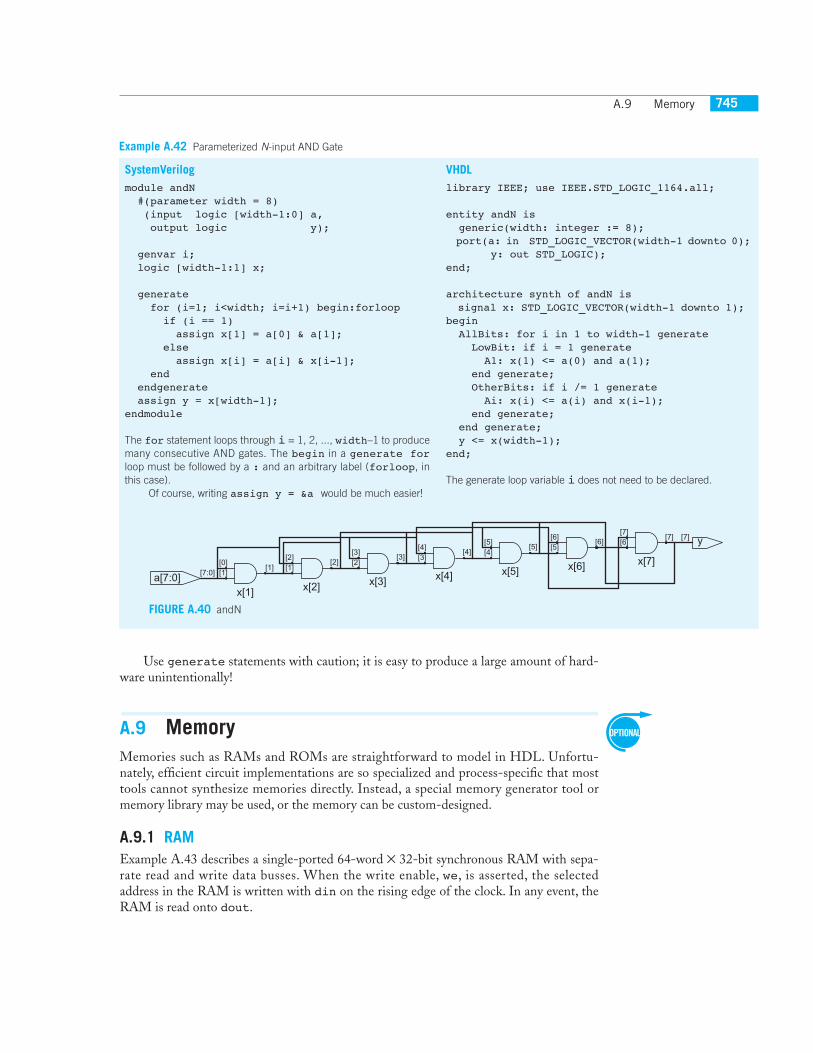
A.9 Memory 745
Use generate statements with caution; it is easy to produce a large amount of hard-ware unintentionally!
A.9 MemoryMemories such as RAMs and ROMs are straightforward to model in HDL. Unfortu-nately, efficient circuit implementations are so specialized and process-specific that mosttools cannot synthesize memories directly. Instead, a special memory generator tool ormemory library may be used, or the memory can be custom-designed.
A.9.1 RAMExample A.43 describes a single-ported 64-word × 32-bit synchronous RAM with sepa-rate read and write data busses. When the write enable, we, is asserted, the selectedaddress in the RAM is written with din on the rising edge of the clock. In any event, theRAM is read onto dout.
Example A.42 Parameterized N-input AND Gate
SystemVerilog
module andN #(parameter width = 8) (input logic [width-1:0] a, output logic y);
genvar i; logic [width-1:1] x;
generate for (i=1; i<width; i=i+1) begin:forloop if (i == 1) assign x[1] = a[0] & a[1]; else assign x[i] = a[i] & x[i-1]; end endgenerate assign y = x[width-1];endmodule
The for statement loops through i = 1, 2, ..., width–1 to producemany consecutive AND gates. The begin in a generate forloop must be followed by a : and an arbitrary label (forloop, inthis case).
Of course, writing assign y = &a would be much easier!
VHDL
library IEEE; use IEEE.STD_LOGIC_1164.all;
entity andN is generic(width: integer := 8); port(a: in STD_LOGIC_VECTOR(width-1 downto 0); y: out STD_LOGIC);end;
architecture synth of andN is signal x: STD_LOGIC_VECTOR(width-1 downto 1); begin AllBits: for i in 1 to width-1 generate LowBit: if i = 1 generate A1: x(1) <= a(0) and a(1); end generate; OtherBits: if i /= 1 generate Ai: x(i) <= a(i) and x(i-1); end generate; end generate; y <= x(width-1);end;
The generate loop variable i does not need to be declared.
x[1] x[2] x[3] x[4] x[5] x[6] x[7]
[7]
[7:0][0]
[1][1]
[2][2]
[1]
[3][3]
[2]
[4][4]
[3]
[5][5]
[4]
[6][6]
[5]
[7][7]
[6]
a[7:0]
y
FIGURE A.40 andN
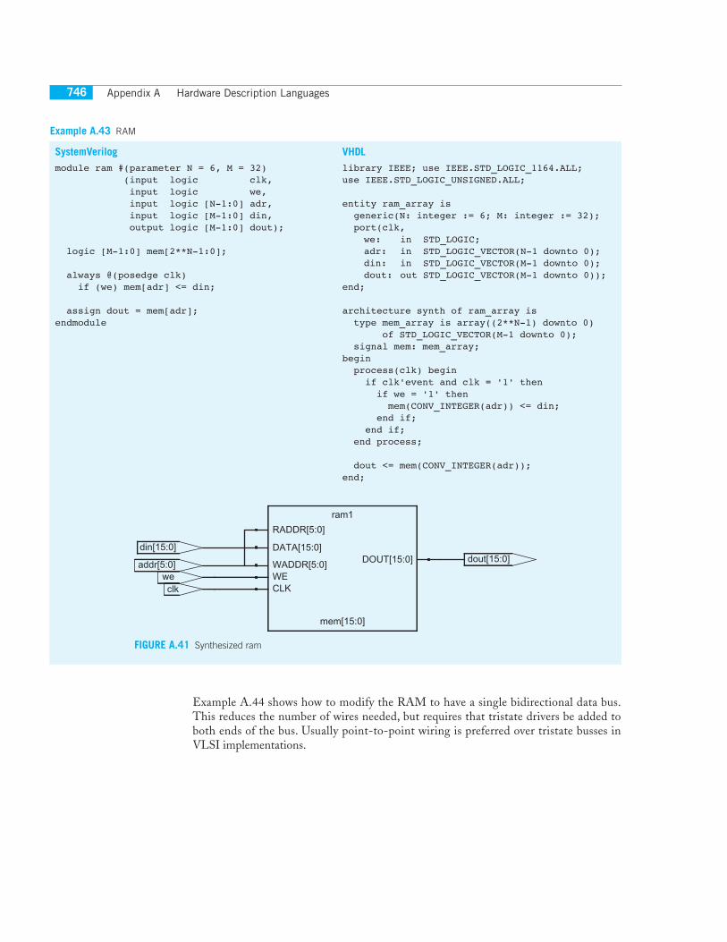
Appendix A Hardware Description Languages746
Example A.44 shows how to modify the RAM to have a single bidirectional data bus.This reduces the number of wires needed, but requires that tristate drivers be added toboth ends of the bus. Usually point-to-point wiring is preferred over tristate busses inVLSI implementations.
Example A.43 RAM
SystemVerilog
module ram #(parameter N = 6, M = 32) (input logic clk, input logic we, input logic [N-1:0] adr, input logic [M-1:0] din, output logic [M-1:0] dout);
logic [M-1:0] mem[2**N-1:0];
always @(posedge clk) if (we) mem[adr] <= din; assign dout = mem[adr];endmodule
VHDL
library IEEE; use IEEE.STD_LOGIC_1164.ALL;use IEEE.STD_LOGIC_UNSIGNED.ALL;
entity ram_array is generic(N: integer := 6; M: integer := 32); port(clk,
we: in STD_LOGIC;adr: in STD_LOGIC_VECTOR(N-1 downto 0);din: in STD_LOGIC_VECTOR(M-1 downto 0);dout: out STD_LOGIC_VECTOR(M-1 downto 0));
end;
architecture synth of ram_array is type mem_array is array((2**N-1) downto 0) of STD_LOGIC_VECTOR(M-1 downto 0); signal mem: mem_array;begin process(clk) begin if clk'event and clk = '1' then if we = '1' then mem(CONV_INTEGER(adr)) <= din; end if; end if; end process; dout <= mem(CONV_INTEGER(adr));end;
ram1
mem[15:0]
dout[15:0]din[15:0]
weaddr[5:0]
clk
RADDR[5:0]
DATA[15:0]DOUT[15:0]WADDR[5:0]
WECLK
FIGURE A.41 Synthesized ram

A.9 Memory 747
Example A.44 RAM with Bidirectional Data Bus
SystemVerilog
module ram #(parameter N = 6, M = 32) (input logic clk, input logic we, input logic [N-1:0] adr, inout tri [M-1:0] data);
logic [M-1:0] mem[2**N-1:0];
always @(posedge clk) if (we) mem[adr] <= data; assign data = we ? 'z : mem[adr];endmodule
Notice that data is declared as an inout port because it can beused both as an input and output. Also, 'z is a shorthand for fillinga bus of arbitrary length with zs.
VHDL
library IEEE; use IEEE.STD_LOGIC_1164.ALL;use IEEE.STD_LOGIC_UNSIGNED.ALL;
entity ram_array is generic(N: integer := 6; M: integer := 32); port(clk,
we: in STD_LOGIC;adr: in STD_LOGIC_VECTOR(N-1 downto 0);data: inout STD_LOGIC_VECTOR(M-1 downto 0));
end;
architecture synth of ram_array is type mem_array is array((2**N-1) downto 0) of STD_LOGIC_VECTOR(M-1 downto 0); signal mem: mem_array;begin process(clk) begin if clk'event and clk = '1' then if we = '1' then mem(CONV_INTEGER(adr)) <= data; end if; end if; end process; data <= (OTHERS => 'Z') when we = '1' else mem(CONV_INTEGER(adr));end;
we
ADR
DATA
N
M
FIGURE A.42 Synthesized ram with bidirectional data bus
A.9.2 Multiported Register FilesA multiported register file has several read and/or write ports. Example A.45 describes asynchronous register file with three ports. Ports 1 and 2 are read ports and port 3 is a writeport.
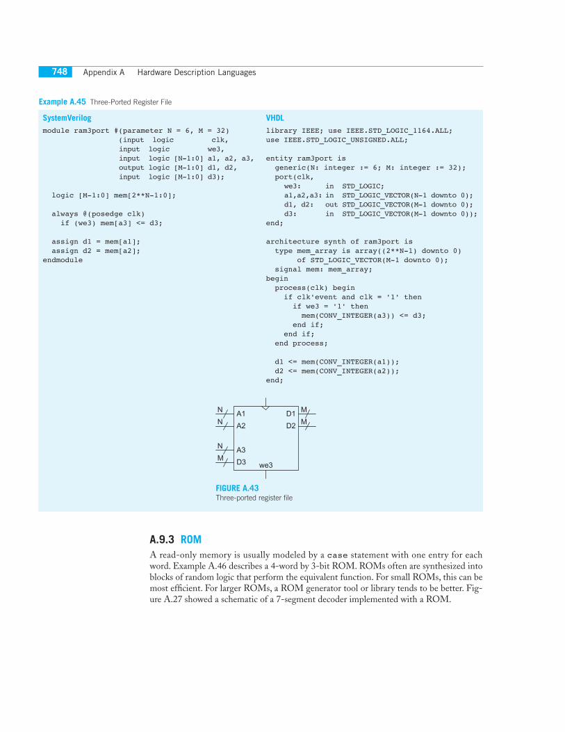
Appendix A Hardware Description Languages748
A.9.3 ROMA read-only memory is usually modeled by a case statement with one entry for eachword. Example A.46 describes a 4-word by 3-bit ROM. ROMs often are synthesized intoblocks of random logic that perform the equivalent function. For small ROMs, this can bemost efficient. For larger ROMs, a ROM generator tool or library tends to be better. Fig-ure A.27 showed a schematic of a 7-segment decoder implemented with a ROM.
Example A.45 Three-Ported Register File
SystemVerilog
module ram3port #(parameter N = 6, M = 32) (input logic clk, input logic we3, input logic [N-1:0] a1, a2, a3, output logic [M-1:0] d1, d2, input logic [M-1:0] d3);
logic [M-1:0] mem[2**N-1:0];
always @(posedge clk) if (we3) mem[a3] <= d3; assign d1 = mem[a1]; assign d2 = mem[a2];endmodule
VHDL
library IEEE; use IEEE.STD_LOGIC_1164.ALL;use IEEE.STD_LOGIC_UNSIGNED.ALL;
entity ram3port is generic(N: integer := 6; M: integer := 32); port(clk,
we3: in STD_LOGIC;a1,a2,a3: in STD_LOGIC_VECTOR(N-1 downto 0);d1, d2: out STD_LOGIC_VECTOR(M-1 downto 0);d3: in STD_LOGIC_VECTOR(M-1 downto 0));
end;
architecture synth of ram3port is type mem_array is array((2**N-1) downto 0) of STD_LOGIC_VECTOR(M-1 downto 0); signal mem: mem_array;begin process(clk) begin if clk'event and clk = '1' then if we3 = '1' then mem(CONV_INTEGER(a3)) <= d3; end if; end if; end process; d1 <= mem(CONV_INTEGER(a1)); d2 <= mem(CONV_INTEGER(a2));end;
we3
A1
A2
A3
D3
D1
D2
N
N
N
M
M
M
FIGURE A.43 Three-ported register file
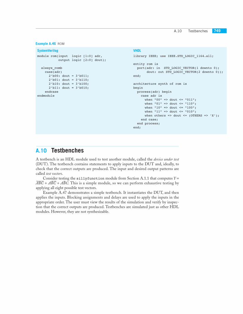
A.10 Testbenches 749
A.10 TestbenchesA testbench is an HDL module used to test another module, called the device under test(DUT). The testbench contains statements to apply inputs to the DUT and, ideally, tocheck that the correct outputs are produced. The input and desired output patterns arecalled test vectors.
Consider testing the sillyfunction module from Section A.1.1 that computes Y =ABC + ABC + ABC. This is a simple module, so we can perform exhaustive testing byapplying all eight possible test vectors.
Example A.47 demonstrates a simple testbench. It instantiates the DUT, and thenapplies the inputs. Blocking assignments and delays are used to apply the inputs in theappropriate order. The user must view the results of the simulation and verify by inspec-tion that the correct outputs are produced. Testbenches are simulated just as other HDLmodules. However, they are not synthesizable.
Example A.46 ROM
SystemVerilog
module rom(input logic [1:0] adr, output logic [2:0] dout);
always_comb case(adr) 2'b00: dout = 3'b011; 2'b01: dout = 3'b110; 2'b10: dout = 3'b100; 2'b11: dout = 3'b010; endcaseendmodule
VHDL
library IEEE; use IEEE.STD_LOGIC_1164.all;
entity rom is port(adr: in STD_LOGIC_VECTOR(1 downto 0); dout: out STD_LOGIC_VECTOR(2 downto 0));end;
architecture synth of rom isbegin process(adr) begin case adr is when "00" => dout <= "011"; when "01" => dout <= "110"; when "10" => dout <= "100"; when "11" => dout <= "010"; when others => dout <= (OTHERS => 'X'); end case; end process;end;
Appendix A Hardware Description Languages750
Checking for correct outputs by hand is tedious and error-prone. Moreover, deter-mining the correct outputs is much easier when the design is fresh in your mind; if youmake minor changes and need to retest weeks later, determining the correct outputsbecomes a hassle. A much better approach is to write a self-checking testbench, shown inExample A.48.
Example A.47 Testbench
SystemVerilog
module testbench1(); logic a, b, c; logic y;
// instantiate device under test sillyfunction dut(a, b, c, y);
// apply inputs one at a time
initial begin a = 0; b = 0; c = 0; #10; c = 1; #10; b = 1; c = 0; #10; c = 1; #10; a = 1; b = 0; c = 0; #10; c = 1; #10; b = 1; c = 0; #10; c = 1; #10; endendmodule
The initial statement executes the statements in its body at thestart of simulation. In this case, it first applies the input pattern 000and waits for 10 time units. It then applies 001 and waits 10 moreunits, and so forth until all eight possible inputs have been applied.Initial statements should only be used in testbenches for simu-lation, not in modules intended to be synthesized into actual hard-ware. Hardware has no way of magically executing a sequence ofspecial steps when it is first turned on.
VHDL
library IEEE; use IEEE.STD_LOGIC_1164.all;
entity testbench1 is -- no inputs or outputsend;
architecture sim of testbench1 is component sillyfunction port(a, b, c: in STD_LOGIC; y: out STD_LOGIC); end component; signal a, b, c, y: STD_LOGIC;begin -- instantiate device under test dut: sillyfunction port map(a, b, c, y);
-- apply inputs one at a time process begin a <= '0'; b <= '0'; c <= '0'; wait for 10 ns; c <= '1'; wait for 10 ns; b <= '1'; c <= '0'; wait for 10 ns; c <= '1'; wait for 10 ns; a <= '1'; b <= '0'; c <= '0'; wait for 10 ns; c <= '1'; wait for 10 ns; b <= '1'; c <= '0'; wait for 10 ns; c <= '1'; wait for 10 ns; wait; -- wait forever end process; end;
The process statement first applies the input pattern 000 andwaits for 10 ns. It then applies 001 and waits 10 more ns, and soforth until all eight possible inputs have been applied.
At the end, the process waits indefinitely; otherwise, the pro-cess would begin again, repeatedly applying the pattern of test vec-tors.
A.10 Testbenches 751
Writing code for each test vector also becomes tedious, especially for modules thatrequire a large number of vectors. An even better approach is to place the test vectors in aseparate file. The testbench simply reads the test vectors, applies the input test vector,waits, checks that the output values match the output vector, and repeats until it reachesthe end of the file.
Example A.49 demonstrates such a testbench. The testbench generates a clock usingan always / process statement with no stimulus list so that it is continuously reevalu-ated. At the beginning of the simulation, it reads the test vectors from a disk file and
Example A.48 Self-Checking Testbench
SystemVerilog
module testbench2(); logic a, b, c; logic y;
// instantiate device under test sillyfunction dut(a, b, c, y);
// apply inputs one at a time // checking results
initial begin a = 0; b = 0; c = 0; #10; assert (y === 1) else $error("000 failed."); c = 1; #10; assert (y === 0) else $error("001 failed."); b = 1; c = 0; #10; assert (y === 0) else $error("010 failed."); c = 1; #10; assert (y === 0) else $error("011 failed."); a = 1; b = 0; c = 0; #10; assert (y === 1) else $error("100 failed."); c = 1; #10; assert (y === 1) else $error("101 failed."); b = 1; c = 0; #10; assert (y === 0) else $error("110 failed."); c = 1; #10; assert (y === 0) else $error("111 failed."); endendmodule
The SystemVerilog assert statement checks if a specified condi-tion is true. If it is not, it executes the else statement. The $errorsystem task in the else statement prints an error message describ-ing the assertion failure. Assert is ignored during synthesis.
In SystemVerilog, comparison using == or != spuriously indi-cates equality if one of the operands is x or z. The === and !==operators must be used instead for testbenches because they workcorrectly with x and z.
VHDL
library IEEE; use IEEE.STD_LOGIC_1164.all;
entity testbench2 is -- no inputs or outputsend;
architecture sim of testbench2 is component sillyfunction port(a, b, c: in STD_LOGIC; y: out STD_LOGIC); end component; signal a, b, c, y: STD_LOGIC;begin -- instantiate device under test dut: sillyfunction port map(a, b, c, y);
-- apply inputs one at a time -- checking results process begin a <= '0'; b <= '0'; c <= '0'; wait for 10 ns; assert y = '1' report "000 failed."; c <= '1'; wait for 10 ns; assert y = '0' report "001 failed."; b <= '1'; c <= '0'; wait for 10 ns; assert y = '0' report "010 failed."; c <= '1'; wait for 10 ns; assert y = '0' report "011 failed."; a <= '1'; b <= '0'; c <= '0'; wait for 10 ns; assert y = '1' report "100 failed."; c <= '1'; wait for 10 ns; assert y = '1' report "101 failed."; b <= '1'; c <= '0'; wait for 10 ns; assert y = '0' report "110 failed."; c <= '1'; wait for 10 ns; assert y = '0' report "111 failed."; wait; -- wait forever end process; end;
The assert statement checks a condition and prints the messagegiven in the report clause if the condition is not satisfied. Assertis ignored during synthesis.
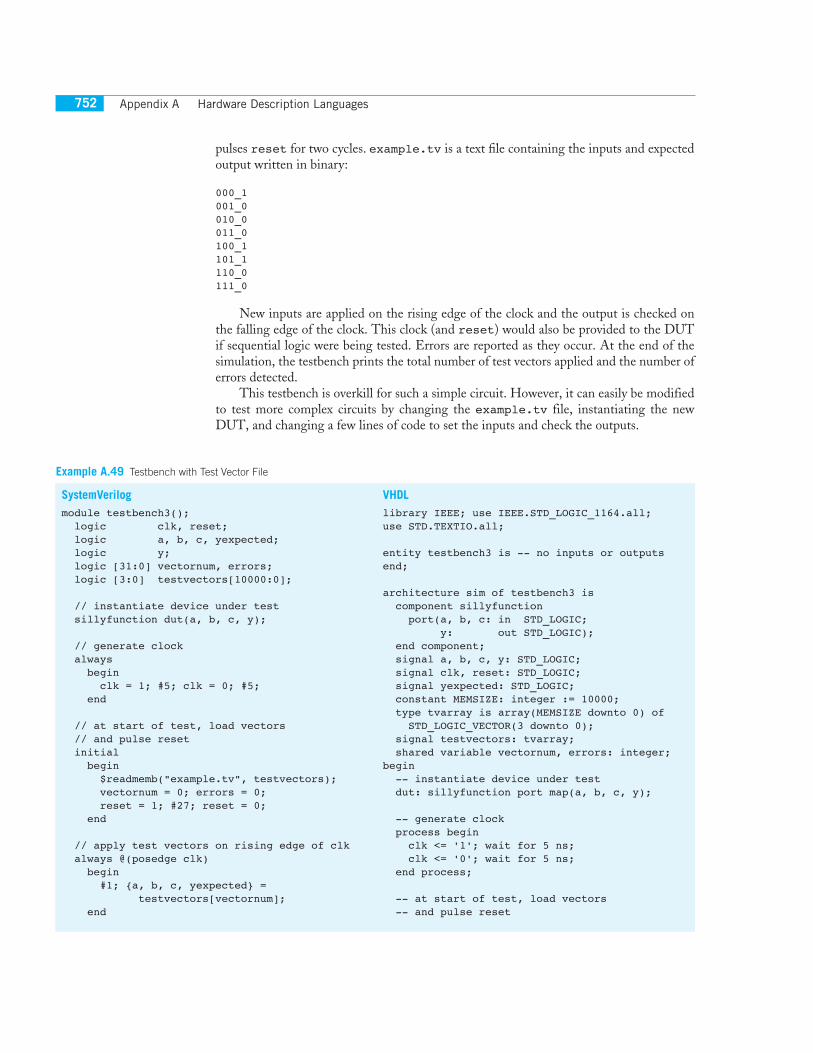
Appendix A Hardware Description Languages752
pulses reset for two cycles. example.tv is a text file containing the inputs and expectedoutput written in binary:
000_1001_0010_0011_0100_1101_1110_0111_0
New inputs are applied on the rising edge of the clock and the output is checked onthe falling edge of the clock. This clock (and reset) would also be provided to the DUTif sequential logic were being tested. Errors are reported as they occur. At the end of thesimulation, the testbench prints the total number of test vectors applied and the number oferrors detected.
This testbench is overkill for such a simple circuit. However, it can easily be modifiedto test more complex circuits by changing the example.tv file, instantiating the newDUT, and changing a few lines of code to set the inputs and check the outputs.
Example A.49 Testbench with Test Vector File
SystemVerilog
module testbench3(); logic clk, reset; logic a, b, c, yexpected; logic y; logic [31:0] vectornum, errors; logic [3:0] testvectors[10000:0];
// instantiate device under test sillyfunction dut(a, b, c, y);
// generate clock always begin clk = 1; #5; clk = 0; #5; end
// at start of test, load vectors // and pulse reset initial begin $readmemb("example.tv", testvectors); vectornum = 0; errors = 0; reset = 1; #27; reset = 0; end
// apply test vectors on rising edge of clk always @(posedge clk) begin #1; {a, b, c, yexpected} = testvectors[vectornum]; end
VHDL
library IEEE; use IEEE.STD_LOGIC_1164.all;use STD.TEXTIO.all;
entity testbench3 is -- no inputs or outputsend;
architecture sim of testbench3 is component sillyfunction port(a, b, c: in STD_LOGIC; y: out STD_LOGIC); end component; signal a, b, c, y: STD_LOGIC; signal clk, reset: STD_LOGIC; signal yexpected: STD_LOGIC; constant MEMSIZE: integer := 10000; type tvarray is array(MEMSIZE downto 0) of STD_LOGIC_VECTOR(3 downto 0); signal testvectors: tvarray; shared variable vectornum, errors: integer;begin -- instantiate device under test dut: sillyfunction port map(a, b, c, y); -- generate clock process begin clk <= '1'; wait for 5 ns; clk <= '0'; wait for 5 ns; end process;
-- at start of test, load vectors -- and pulse reset
A.10 Testbenches 753
SystemVerilog (continued) // check results on falling edge of clk always @(negedge clk) if (~reset) begin // skip during reset if (y !== yexpected) begin
$display("Error: inputs = %b", {a, b, c});$display(" outputs = %b (%b expected)",
y, yexpected); errors = errors + 1; end vectornum = vectornum + 1; if (testvectors[vectornum] === 'bx) begin
$display("%d tests completed with %d errors", vectornum, errors);
$finish; end endendmodule
$readmemb reads a file of binary numbers into an array.$readmemh is similar, but it reads a file of hexadecimal numbers.
The next block of code waits one time unit after the rising edgeof the clock (to avoid any confusion of clock and data changingsimultaneously), then sets the three inputs and the expected outputbased on the 4 bits in the current test vector.
$display is a system task to print in the simulator window.$finish terminates the simulation.
Note that even though the SystemVerilog module supports upto 10001 test vectors, it will terminate the simulation after executingthe 8 vectors in the file.
For more information on testbenches and SystemVerilog verifi-cation, consult [Bergeron05].
VHDL (continued) process is file tv: TEXT; variable i, j: integer; variable L: line; variable ch: character; begin -- read file of test vectors i := 0; FILE_OPEN(tv, "example.tv", READ_MODE); while not endfile(tv) loop readline(tv, L); for j in 0 to 3 loop read(L, ch); if (ch = '_') then read(L, ch); end if; if (ch = '0') then testvectors(i)(j) <= '0'; else testvectors(i)(j) <= '1'; end if; end loop; i := i + 1; end loop;
vectornum := 0; errors := 0; reset <= '1'; wait for 27 ns; reset <= '0'; wait; end process; -- apply test vectors on rising edge of clk process (clk) begin if (clk'event and clk = '1') then a <= testvectors(vectornum)(0) after 1 ns; b <= testvectors(vectornum)(1) after 1 ns; c <= testvectors(vectornum)(2) after 1 ns; yexpected <= testvectors(vectornum)(3) after 1 ns; end if; end process;
-- check results on falling edge of clk process (clk) begin if (clk'event and clk = '0' and reset = '0') then assert y = yexpected report "Error: y = " & STD_LOGIC'image(y); if (y /= yexpected) then errors := errors + 1; end if; vectornum := vectornum + 1; if (is_x(testvectors(vectornum))) then if (errors = 0) then report "Just kidding -- " & integer'image(vectornum) & " tests completed successfully." severity failure;
(continues)
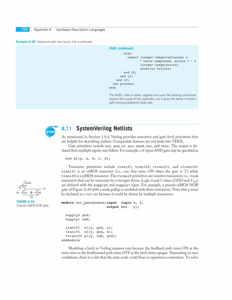
Appendix A Hardware Description Languages754
A.11 SystemVerilog NetlistsAs mentioned in Section 1.8.4, Verilog provides transistor and gate-level primitives thatare helpful for describing netlists. Comparable features are not built into VHDL.
Gate primitives include not, and, or, xor, nand, nor, and xnor. The output is de-clared first; multiple inputs may follow. For example, a 4-input AND gate may be specified as
and g1(y, a, b, c, d);
Transistor primitives include tranif1, tranif0, rtranif1, and rtranif0.tranif1 is an nMOS transistor (i.e., one that turns ON when the gate is ‘1’) whiletranif0 is a pMOS transistor. The rtranif primitives are resistive transistors; i.e., weaktransistors that can be overcome by a stronger driver. Logic 0 and 1 values (GND and VDD)are defined with the supply0 and supply1 types. For example, a pseudo-nMOS NORgate of Figure A.44 with a weak pullup is modeled with three transistors. Note that y mustbe declared as a tri net because it could be driven by multiple transistors.
module nor_pseudonmos(input logic a, b, output tri y);
supply0 gnd; supply1 vdd;
tranif1 n1(y, gnd, a); tranif1 n2(y, gnd, b); rtranif0 p1(y, vdd, gnd);endmodule
Modeling a latch in Verilog requires care because the feedback path turns ON at thesame time as the feedforward path turns OFF as the latch turns opaque. Depending on raceconditions, there is a risk that the state node could float or experience contention. To solve
Example A.49 Testbench with Test Vector File (continued)
VHDL (continued) else report integer'image(vectornum) & " tests completed, errors = " & integer'image(errors) severity failure; end if; end if; end if; end process;end;
The VHDL code is rather ungainly and uses file reading commandsbeyond the scope of this appendix, but it gives the sense of what aself-checking testbench looks like.
A BY
N1 N2
P1weak
FIGURE A.44 Pseudo-nMOS NOR gate

A.12 Example: MIPS Processor 755
this problem, the state node is modeled as a trireg (so it will not float) and the feed-back transistors are modeled as weak (so they will not cause contention). The othernodes are tri nets because they can be driven by multiple transistors. Figure A.45 re-draws the latch from Figure 10.17(g) at the transistor level and highlights the weaktransistors and state node.
module latch(input logic ph, phb, d, output tri q);
trireg x; tri xb, nn12, nn56, pp12, pp56; supply0 gnd; supply1 vdd;
// input stage tranif1 n1(nn12, gnd, d); tranif1 n2(x, nn12, ph); tranif0 p1(pp12, vdd, d); tranif0 p2(x, pp12, phb);
// output inverter tranif1 n3(q, gnd, x); tranif0 p3(q, vdd, x);
// xb inverter tranif1 n4(xb, gnd, x); tranif0 p4(xb, vdd, x);
// feedback tristate tranif1 n5(nn56, gnd, xb); rtranif1 n6(x, nn56, phb); tranif0 p5(pp56, vdd, xb); rtranif0 p6(x, pp56, ph);endmodule
Most synthesis tools map only onto gates, not transistors, so transistor primitivesare only for simulation.
The tranif devices are bidirectional; i.e., the source and drain are symmetric.Verilog also supports unidirectional nmos and pmos primitives that only allow a signalto flow from the input terminal to the output terminal. Real transistors are inherentlybidirectional, so unidirectional models can result in simulation not catching bugs thatwould exist in real hardware. Therefore, tranif primitives are preferred for simulation.
A.12 Example: MIPS ProcessorTo illustrate a nontrivial HDL design, this section lists the code and testbench for theMIPS processor subset discussed in Chapter 1. The example handles only the LB, SB,ADD, SUB, AND, OR, SLT, BEQ, and J instructions. It uses an 8-bit datapath and onlyeight registers. Because the instruction is 32-bits wide, it is loaded in four successivefetch cycles across an 8-bit path to external memory.
N1
N2
P2
P1
N5
N6
P6
P5
DX
Q
X
φ
φ
φ
φ
N4
P4
N3
P3
trireg
weakweak
FIGURE A.45 latch
Appendix A Hardware Description Languages756
A.12.1 TestbenchThe testbench initializes a 256-byte memory with instructions and data from a text file.The code exercises each of the instructions. The mipstest.asm assembly language fileand memfile.dat text file are shown below. The testbench runs until it observes a mem-ory write. If the value 7 is written to address 76, the code probably executed correctly. If allgoes well, the testbench should take 100 cycles (1000 ns) to run.
# mipstest.asm# 9/16/03 David Harris [email protected]## Test MIPS instructions. Assumes little-endian memory was# initialized as:# word 16: 3# word 17: 5# word 18: 12
main: #Assembly Code effect Machine Code lb $2, 68($0) # initialize $2 = 5 80020044lb $7, 64($0) # initialize $7 = 3 80070040lb $3, 69($7) # initialize $3 = 12 80e30045or $4, $7, $2 # $4 <= 3 or 5 = 7 00e22025and $5, $3, $4 # $5 <= 12 and 7 = 4 00642824add $5, $5, $4 # $5 <= 4 + 7 = 11 00a42820beq $5, $7, end # shouldn’t be taken 10a70008slt $6, $3, $4 # $6 <= 12 < 7 = 0 0064302abeq $6, $0, around # should be taken 10c00001lb $5, 0($0) # shouldn’t happen 80050000
around: slt $6, $7, $2 # $6 <= 3 < 5 = 1 00e2302aadd $7, $6, $5 # $7 <= 1 + 11 = 12 00c53820sub $7, $7, $2 # $7 <= 12 - 5 = 7 00e23822j end # should be taken 0800000flb $7, 0($0) # shouldn’t happen 80070000
end: sb $7, 71($2) # write adr 76 <= 7 a0470047.dw 3 00000003.dw 5 00000005.dw 12 0000000c
memfile.dat800200448007004080e3004500e220250064282400a4282010a700080064302a10c000018005000000e2302a00c5382000e238220800000f80070000a047004700000003000000050000000c
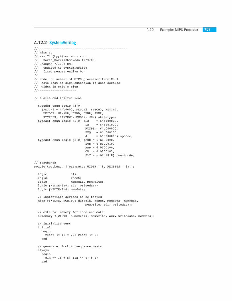
A.12 Example: MIPS Processor 757
A.12.2 SystemVerilog//-------------------------------------------------// mips.sv// Max Yi ([email protected]) and // [email protected] 12/9/03// Changes 7/3/07 DMH// Updated to SystemVerilog// fixed memory endian bug//// Model of subset of MIPS processor from Ch 1// note that no sign extension is done because // width is only 8 bits//---------------------
// states and instructions
typedef enum logic [3:0] {FETCH1 = 4'b0000, FETCH2, FETCH3, FETCH4, DECODE, MEMADR, LBRD, LBWR, SBWR, RTYPEEX, RTYPEWR, BEQEX, JEX} statetype; typedef enum logic [5:0] {LB = 6'b100000, SB = 6'b101000, RTYPE = 6'b000000, BEQ = 6'b000100, J = 6'b000010} opcode; typedef enum logic [5:0] {ADD = 6'b100000, SUB = 6'b100010, AND = 6'b100100, OR = 6'b100101, SLT = 6'b101010} functcode;
// testbenchmodule testbench #(parameter WIDTH = 8, REGBITS = 3)();
logic clk; logic reset; logic memread, memwrite; logic [WIDTH-1:0] adr, writedata; logic [WIDTH-1:0] memdata;
// instantiate devices to be tested mips #(WIDTH,REGBITS) dut(clk, reset, memdata, memread, memwrite, adr, writedata);
// external memory for code and data exmemory #(WIDTH) exmem(clk, memwrite, adr, writedata, memdata);
// initialize test initial begin reset <= 1; # 22; reset <= 0; end
// generate clock to sequence tests always begin clk <= 1; # 5; clk <= 0; # 5; end
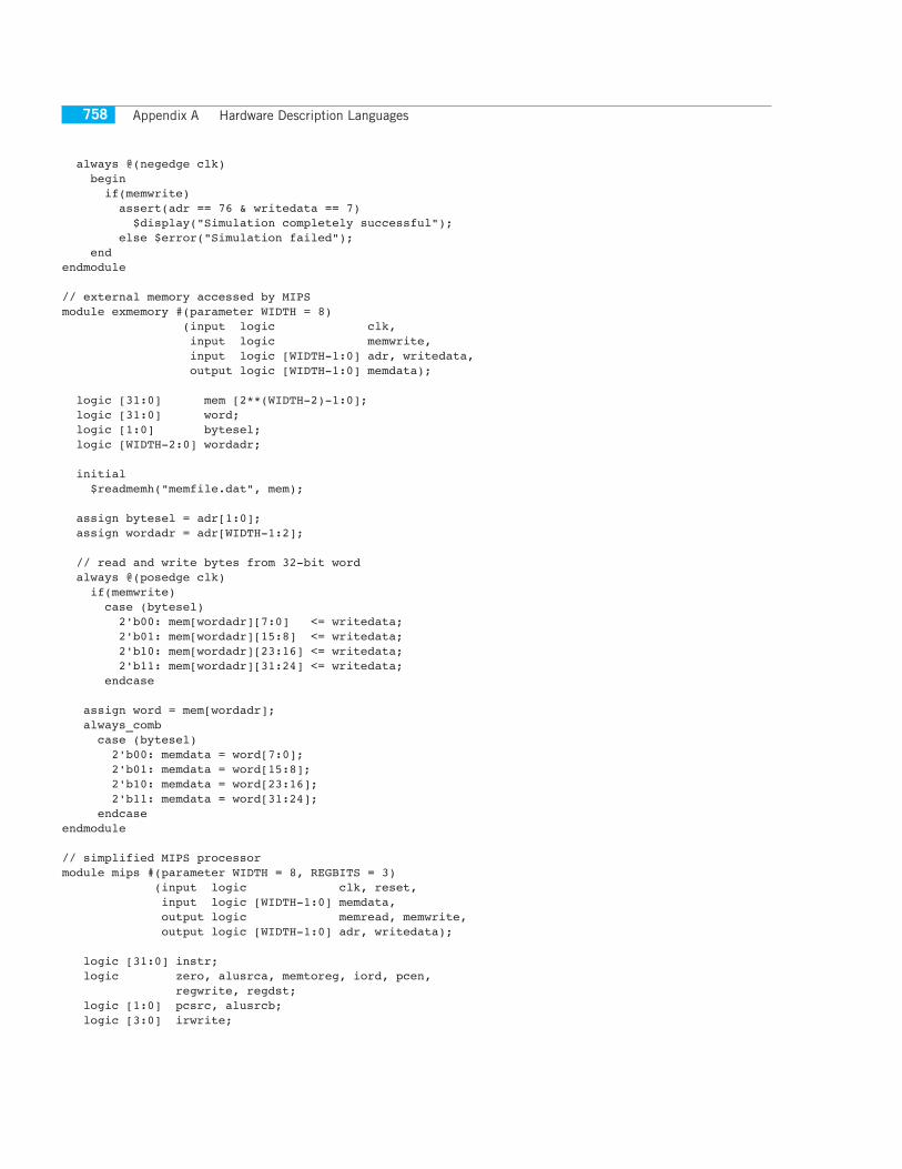
Appendix A Hardware Description Languages758
always @(negedge clk) begin if(memwrite) assert(adr == 76 & writedata == 7) $display("Simulation completely successful"); else $error("Simulation failed"); endendmodule
// external memory accessed by MIPSmodule exmemory #(parameter WIDTH = 8) (input logic clk, input logic memwrite, input logic [WIDTH-1:0] adr, writedata, output logic [WIDTH-1:0] memdata);
logic [31:0] mem [2**(WIDTH-2)-1:0]; logic [31:0] word; logic [1:0] bytesel; logic [WIDTH-2:0] wordadr;
initial $readmemh("memfile.dat", mem);
assign bytesel = adr[1:0]; assign wordadr = adr[WIDTH-1:2];
// read and write bytes from 32-bit word always @(posedge clk) if(memwrite) case (bytesel) 2'b00: mem[wordadr][7:0] <= writedata; 2'b01: mem[wordadr][15:8] <= writedata; 2'b10: mem[wordadr][23:16] <= writedata; 2'b11: mem[wordadr][31:24] <= writedata; endcase
assign word = mem[wordadr]; always_comb case (bytesel) 2'b00: memdata = word[7:0]; 2'b01: memdata = word[15:8]; 2'b10: memdata = word[23:16]; 2'b11: memdata = word[31:24]; endcaseendmodule
// simplified MIPS processormodule mips #(parameter WIDTH = 8, REGBITS = 3) (input logic clk, reset, input logic [WIDTH-1:0] memdata, output logic memread, memwrite, output logic [WIDTH-1:0] adr, writedata);
logic [31:0] instr; logic zero, alusrca, memtoreg, iord, pcen, regwrite, regdst; logic [1:0] pcsrc, alusrcb; logic [3:0] irwrite;
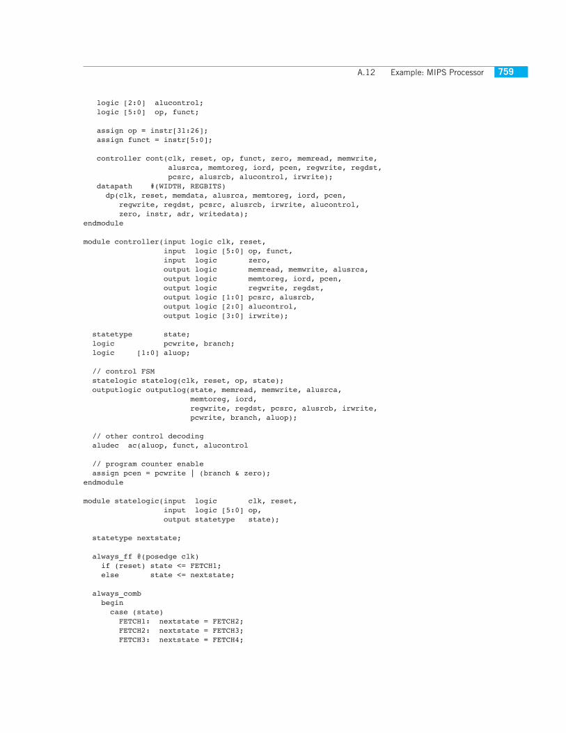
A.12 Example: MIPS Processor 759
logic [2:0] alucontrol; logic [5:0] op, funct; assign op = instr[31:26]; assign funct = instr[5:0]; controller cont(clk, reset, op, funct, zero, memread, memwrite, alusrca, memtoreg, iord, pcen, regwrite, regdst, pcsrc, alusrcb, alucontrol, irwrite); datapath #(WIDTH, REGBITS) dp(clk, reset, memdata, alusrca, memtoreg, iord, pcen, regwrite, regdst, pcsrc, alusrcb, irwrite, alucontrol, zero, instr, adr, writedata);endmodule
module controller(input logic clk, reset, input logic [5:0] op, funct, input logic zero, output logic memread, memwrite, alusrca, output logic memtoreg, iord, pcen, output logic regwrite, regdst, output logic [1:0] pcsrc, alusrcb, output logic [2:0] alucontrol, output logic [3:0] irwrite);
statetype state; logic pcwrite, branch; logic [1:0] aluop;
// control FSM statelogic statelog(clk, reset, op, state); outputlogic outputlog(state, memread, memwrite, alusrca, memtoreg, iord, regwrite, regdst, pcsrc, alusrcb, irwrite, pcwrite, branch, aluop);
// other control decoding aludec ac(aluop, funct, alucontrol
// program counter enable assign pcen = pcwrite | (branch & zero); endmodule
module statelogic(input logic clk, reset, input logic [5:0] op, output statetype state);
statetype nextstate; always_ff @(posedge clk) if (reset) state <= FETCH1; else state <= nextstate; always_comb begin case (state) FETCH1: nextstate = FETCH2; FETCH2: nextstate = FETCH3; FETCH3: nextstate = FETCH4;
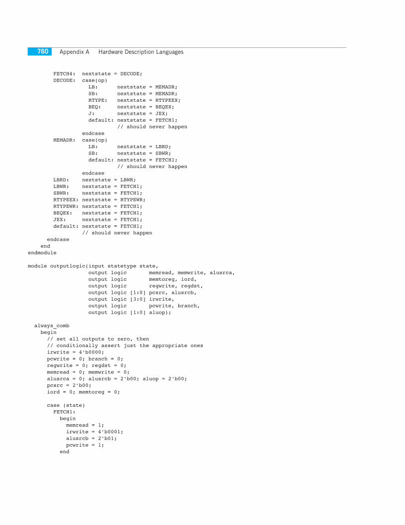
Appendix A Hardware Description Languages760
FETCH4: nextstate = DECODE; DECODE: case(op) LB: nextstate = MEMADR; SB: nextstate = MEMADR; RTYPE: nextstate = RTYPEEX; BEQ: nextstate = BEQEX; J: nextstate = JEX; default: nextstate = FETCH1; // should never happen endcase MEMADR: case(op) LB: nextstate = LBRD; SB: nextstate = SBWR; default: nextstate = FETCH1; // should never happen endcase LBRD: nextstate = LBWR; LBWR: nextstate = FETCH1; SBWR: nextstate = FETCH1; RTYPEEX: nextstate = RTYPEWR; RTYPEWR: nextstate = FETCH1; BEQEX: nextstate = FETCH1; JEX: nextstate = FETCH1; default: nextstate = FETCH1; // should never happen endcase endendmodule
module outputlogic(input statetype state, output logic memread, memwrite, alusrca, output logic memtoreg, iord, output logic regwrite, regdst, output logic [1:0] pcsrc, alusrcb, output logic [3:0] irwrite, output logic pcwrite, branch, output logic [1:0] aluop);
always_comb begin // set all outputs to zero, then // conditionally assert just the appropriate ones irwrite = 4'b0000; pcwrite = 0; branch = 0; regwrite = 0; regdst = 0; memread = 0; memwrite = 0; alusrca = 0; alusrcb = 2'b00; aluop = 2'b00; pcsrc = 2'b00; iord = 0; memtoreg = 0;
case (state) FETCH1: begin memread = 1; irwrite = 4'b0001; alusrcb = 2'b01; pcwrite = 1; end
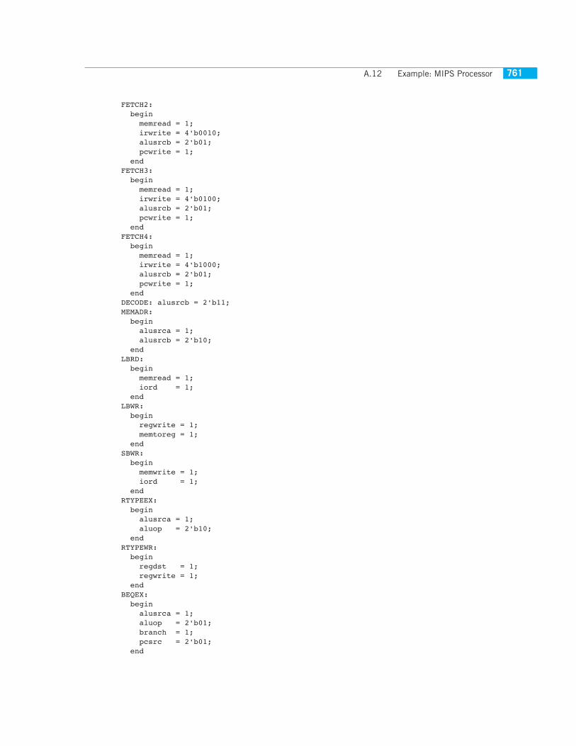
A.12 Example: MIPS Processor 761
FETCH2: begin memread = 1; irwrite = 4'b0010; alusrcb = 2'b01; pcwrite = 1; end FETCH3: begin memread = 1; irwrite = 4'b0100; alusrcb = 2'b01; pcwrite = 1; end FETCH4: begin memread = 1; irwrite = 4'b1000; alusrcb = 2'b01; pcwrite = 1; end DECODE: alusrcb = 2'b11; MEMADR: begin alusrca = 1; alusrcb = 2'b10; end LBRD: begin memread = 1; iord = 1; end LBWR: begin regwrite = 1; memtoreg = 1; end SBWR: begin memwrite = 1; iord = 1; end RTYPEEX: begin alusrca = 1; aluop = 2'b10; end RTYPEWR: begin regdst = 1; regwrite = 1; end BEQEX: begin alusrca = 1; aluop = 2'b01; branch = 1; pcsrc = 2'b01; end
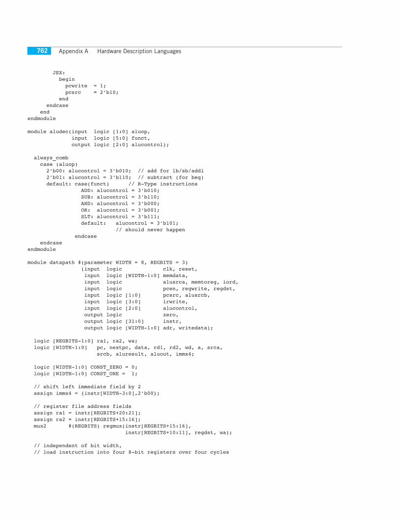
Appendix A Hardware Description Languages762
JEX: begin pcwrite = 1; pcsrc = 2'b10; end endcase endendmodule
module aludec(input logic [1:0] aluop, input logic [5:0] funct, output logic [2:0] alucontrol);
always_comb case (aluop) 2'b00: alucontrol = 3'b010; // add for lb/sb/addi 2'b01: alucontrol = 3'b110; // subtract (for beq) default: case(funct) // R-Type instructions ADD: alucontrol = 3'b010; SUB: alucontrol = 3'b110; AND: alucontrol = 3'b000; OR: alucontrol = 3'b001; SLT: alucontrol = 3'b111; default: alucontrol = 3'b101; // should never happen endcase endcaseendmodule
module datapath #(parameter WIDTH = 8, REGBITS = 3) (input logic clk, reset, input logic [WIDTH-1:0] memdata, input logic alusrca, memtoreg, iord, input logic pcen, regwrite, regdst, input logic [1:0] pcsrc, alusrcb, input logic [3:0] irwrite, input logic [2:0] alucontrol, output logic zero, output logic [31:0] instr, output logic [WIDTH-1:0] adr, writedata);
logic [REGBITS-1:0] ra1, ra2, wa; logic [WIDTH-1:0] pc, nextpc, data, rd1, rd2, wd, a, srca, srcb, aluresult, aluout, immx4;
logic [WIDTH-1:0] CONST_ZERO = 0; logic [WIDTH-1:0] CONST_ONE = 1;
// shift left immediate field by 2 assign immx4 = {instr[WIDTH-3:0],2'b00};
// register file address fields assign ra1 = instr[REGBITS+20:21]; assign ra2 = instr[REGBITS+15:16]; mux2 #(REGBITS) regmux(instr[REGBITS+15:16], instr[REGBITS+10:11], regdst, wa);
// independent of bit width, // load instruction into four 8-bit registers over four cycles
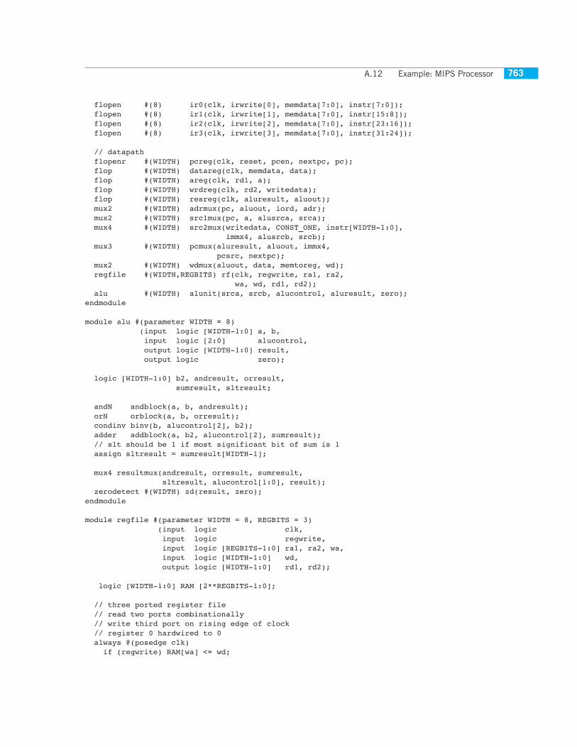
A.12 Example: MIPS Processor 763
flopen #(8) ir0(clk, irwrite[0], memdata[7:0], instr[7:0]); flopen #(8) ir1(clk, irwrite[1], memdata[7:0], instr[15:8]); flopen #(8) ir2(clk, irwrite[2], memdata[7:0], instr[23:16]); flopen #(8) ir3(clk, irwrite[3], memdata[7:0], instr[31:24]);
// datapath flopenr #(WIDTH) pcreg(clk, reset, pcen, nextpc, pc); flop #(WIDTH) datareg(clk, memdata, data); flop #(WIDTH) areg(clk, rd1, a); flop #(WIDTH) wrdreg(clk, rd2, writedata); flop #(WIDTH) resreg(clk, aluresult, aluout); mux2 #(WIDTH) adrmux(pc, aluout, iord, adr); mux2 #(WIDTH) src1mux(pc, a, alusrca, srca); mux4 #(WIDTH) src2mux(writedata, CONST_ONE, instr[WIDTH-1:0], immx4, alusrcb, srcb); mux3 #(WIDTH) pcmux(aluresult, aluout, immx4, pcsrc, nextpc); mux2 #(WIDTH) wdmux(aluout, data, memtoreg, wd); regfile #(WIDTH,REGBITS) rf(clk, regwrite, ra1, ra2, wa, wd, rd1, rd2); alu #(WIDTH) alunit(srca, srcb, alucontrol, aluresult, zero);endmodule
module alu #(parameter WIDTH = 8) (input logic [WIDTH-1:0] a, b, input logic [2:0] alucontrol, output logic [WIDTH-1:0] result, output logic zero);
logic [WIDTH-1:0] b2, andresult, orresult, sumresult, sltresult;
andN andblock(a, b, andresult); orN orblock(a, b, orresult); condinv binv(b, alucontrol[2], b2); adder addblock(a, b2, alucontrol[2], sumresult); // slt should be 1 if most significant bit of sum is 1 assign sltresult = sumresult[WIDTH-1];
mux4 resultmux(andresult, orresult, sumresult, sltresult, alucontrol[1:0], result); zerodetect #(WIDTH) zd(result, zero);endmodule
module regfile #(parameter WIDTH = 8, REGBITS = 3) (input logic clk, input logic regwrite, input logic [REGBITS-1:0] ra1, ra2, wa, input logic [WIDTH-1:0] wd, output logic [WIDTH-1:0] rd1, rd2);
logic [WIDTH-1:0] RAM [2**REGBITS-1:0];
// three ported register file // read two ports combinationally // write third port on rising edge of clock // register 0 hardwired to 0 always @(posedge clk) if (regwrite) RAM[wa] <= wd;
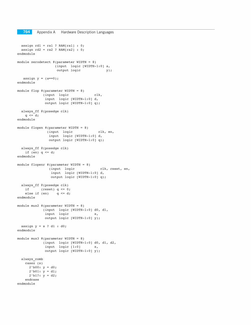
Appendix A Hardware Description Languages764
assign rd1 = ra1 ? RAM[ra1] : 0; assign rd2 = ra2 ? RAM[ra2] : 0;endmodule
module zerodetect #(parameter WIDTH = 8) (input logic [WIDTH-1:0] a, output logic y);
assign y = (a==0);endmodule
module flop #(parameter WIDTH = 8) (input logic clk, input logic [WIDTH-1:0] d, output logic [WIDTH-1:0] q);
always_ff @(posedge clk) q <= d;endmodule
module flopen #(parameter WIDTH = 8) (input logic clk, en, input logic [WIDTH-1:0] d, output logic [WIDTH-1:0] q);
always_ff @(posedge clk) if (en) q <= d;endmodule
module flopenr #(parameter WIDTH = 8) (input logic clk, reset, en, input logic [WIDTH-1:0] d, output logic [WIDTH-1:0] q); always_ff @(posedge clk) if (reset) q <= 0; else if (en) q <= d;endmodule
module mux2 #(parameter WIDTH = 8) (input logic [WIDTH-1:0] d0, d1, input logic s, output logic [WIDTH-1:0] y);
assign y = s ? d1 : d0; endmodule
module mux3 #(parameter WIDTH = 8) (input logic [WIDTH-1:0] d0, d1, d2, input logic [1:0] s, output logic [WIDTH-1:0] y);
always_comb casez (s) 2'b00: y = d0; 2'b01: y = d1; 2'b1?: y = d2; endcaseendmodule
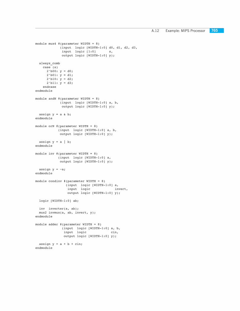
A.12 Example: MIPS Processor 765
module mux4 #(parameter WIDTH = 8) (input logic [WIDTH-1:0] d0, d1, d2, d3, input logic [1:0] s, output logic [WIDTH-1:0] y);
always_comb case (s) 2'b00: y = d0; 2'b01: y = d1; 2'b10: y = d2; 2'b11: y = d3; endcaseendmodule
module andN #(parameter WIDTH = 8) (input logic [WIDTH-1:0] a, b, output logic [WIDTH-1:0] y);
assign y = a & b;endmodule
module orN #(parameter WIDTH = 8) (input logic [WIDTH-1:0] a, b, output logic [WIDTH-1:0] y);
assign y = a | b;endmodule
module inv #(parameter WIDTH = 8) (input logic [WIDTH-1:0] a, output logic [WIDTH-1:0] y);
assign y = ~a;endmodule
module condinv #(parameter WIDTH = 8) (input logic [WIDTH-1:0] a, input logic invert, output logic [WIDTH-1:0] y);
logic [WIDTH-1:0] ab;
inv inverter(a, ab); mux2 invmux(a, ab, invert, y);endmodule
module adder #(parameter WIDTH = 8) (input logic [WIDTH-1:0] a, b, input logic cin, output logic [WIDTH-1:0] y);
assign y = a + b + cin;endmodule
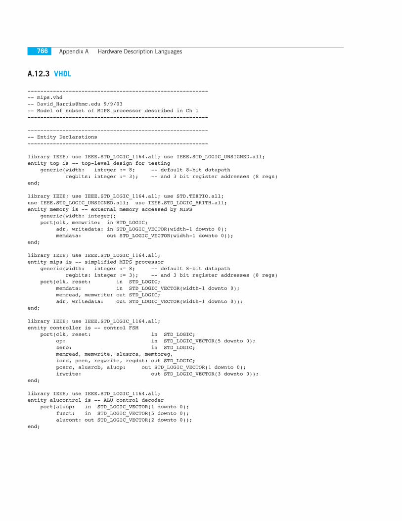
Appendix A Hardware Description Languages766
A.12.3 VHDL
----------------------------------------------------------- mips.vhd-- [email protected] 9/9/03-- Model of subset of MIPS processor described in Ch 1---------------------------------------------------------
----------------------------------------------------------- Entity Declarations---------------------------------------------------------
library IEEE; use IEEE.STD_LOGIC_1164.all; use IEEE.STD_LOGIC_UNSIGNED.all;entity top is -- top-level design for testing generic(width: integer := 8; -- default 8-bit datapath regbits: integer := 3); -- and 3 bit register addresses (8 regs)end;
library IEEE; use IEEE.STD_LOGIC_1164.all; use STD.TEXTIO.all;use IEEE.STD_LOGIC_UNSIGNED.all; use IEEE.STD_LOGIC_ARITH.all;entity memory is -- external memory accessed by MIPS generic(width: integer); port(clk, memwrite: in STD_LOGIC; adr, writedata: in STD_LOGIC_VECTOR(width-1 downto 0); memdata: out STD_LOGIC_VECTOR(width-1 downto 0));end;
library IEEE; use IEEE.STD_LOGIC_1164.all;entity mips is -- simplified MIPS processor generic(width: integer := 8; -- default 8-bit datapath regbits: integer := 3); -- and 3 bit register addresses (8 regs) port(clk, reset: in STD_LOGIC; memdata: in STD_LOGIC_VECTOR(width-1 downto 0); memread, memwrite: out STD_LOGIC; adr, writedata: out STD_LOGIC_VECTOR(width-1 downto 0));end;
library IEEE; use IEEE.STD_LOGIC_1164.all;entity controller is -- control FSM port(clk, reset: in STD_LOGIC; op: in STD_LOGIC_VECTOR(5 downto 0); zero: in STD_LOGIC; memread, memwrite, alusrca, memtoreg, iord, pcen, regwrite, regdst: out STD_LOGIC; pcsrc, alusrcb, aluop: out STD_LOGIC_VECTOR(1 downto 0); irwrite: out STD_LOGIC_VECTOR(3 downto 0));end;
library IEEE; use IEEE.STD_LOGIC_1164.all;entity alucontrol is -- ALU control decoder port(aluop: in STD_LOGIC_VECTOR(1 downto 0); funct: in STD_LOGIC_VECTOR(5 downto 0); alucont: out STD_LOGIC_VECTOR(2 downto 0));end;
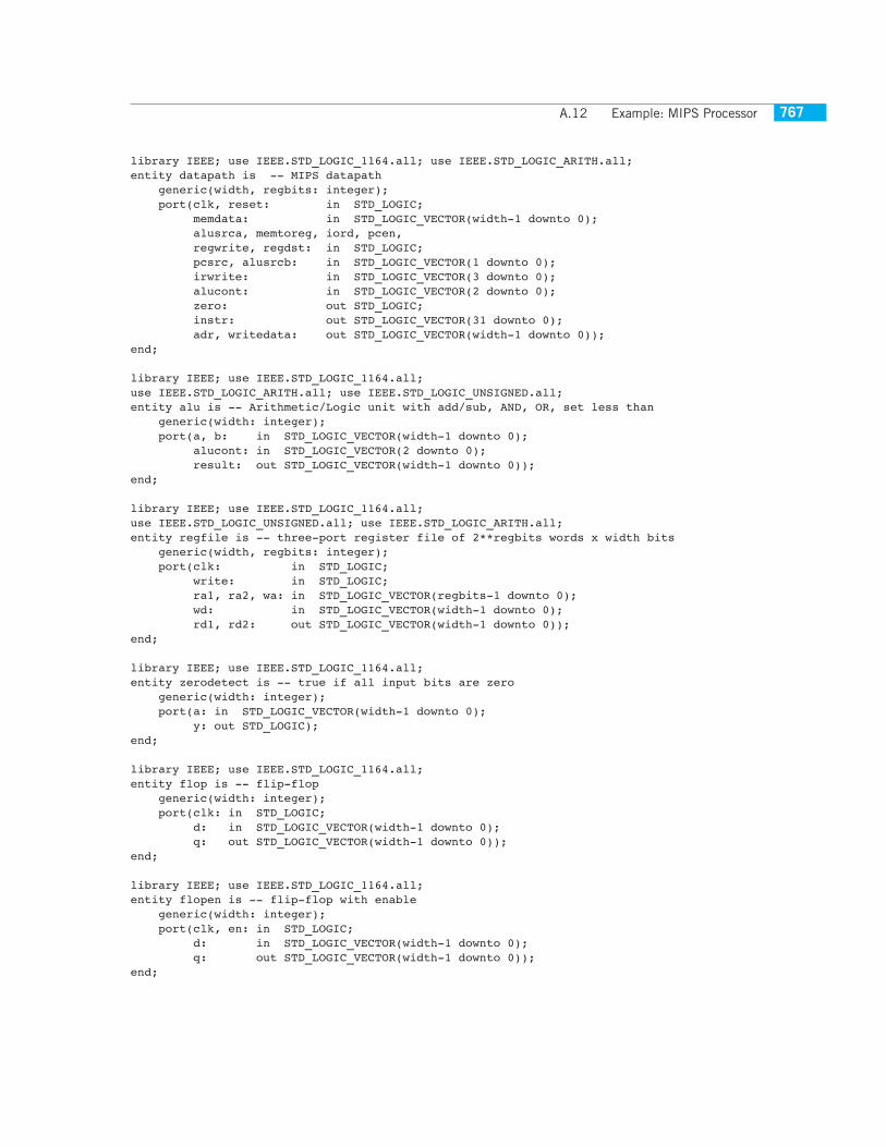
A.12 Example: MIPS Processor 767
library IEEE; use IEEE.STD_LOGIC_1164.all; use IEEE.STD_LOGIC_ARITH.all;entity datapath is -- MIPS datapath generic(width, regbits: integer); port(clk, reset: in STD_LOGIC; memdata: in STD_LOGIC_VECTOR(width-1 downto 0); alusrca, memtoreg, iord, pcen, regwrite, regdst: in STD_LOGIC; pcsrc, alusrcb: in STD_LOGIC_VECTOR(1 downto 0); irwrite: in STD_LOGIC_VECTOR(3 downto 0); alucont: in STD_LOGIC_VECTOR(2 downto 0); zero: out STD_LOGIC; instr: out STD_LOGIC_VECTOR(31 downto 0); adr, writedata: out STD_LOGIC_VECTOR(width-1 downto 0));end;
library IEEE; use IEEE.STD_LOGIC_1164.all; use IEEE.STD_LOGIC_ARITH.all; use IEEE.STD_LOGIC_UNSIGNED.all;entity alu is -- Arithmetic/Logic unit with add/sub, AND, OR, set less than generic(width: integer); port(a, b: in STD_LOGIC_VECTOR(width-1 downto 0); alucont: in STD_LOGIC_VECTOR(2 downto 0); result: out STD_LOGIC_VECTOR(width-1 downto 0));end;
library IEEE; use IEEE.STD_LOGIC_1164.all; use IEEE.STD_LOGIC_UNSIGNED.all; use IEEE.STD_LOGIC_ARITH.all;entity regfile is -- three-port register file of 2**regbits words x width bits generic(width, regbits: integer); port(clk: in STD_LOGIC; write: in STD_LOGIC; ra1, ra2, wa: in STD_LOGIC_VECTOR(regbits-1 downto 0); wd: in STD_LOGIC_VECTOR(width-1 downto 0); rd1, rd2: out STD_LOGIC_VECTOR(width-1 downto 0));end;
library IEEE; use IEEE.STD_LOGIC_1164.all;entity zerodetect is -- true if all input bits are zero generic(width: integer); port(a: in STD_LOGIC_VECTOR(width-1 downto 0); y: out STD_LOGIC);end;
library IEEE; use IEEE.STD_LOGIC_1164.all;entity flop is -- flip-flop generic(width: integer); port(clk: in STD_LOGIC; d: in STD_LOGIC_VECTOR(width-1 downto 0); q: out STD_LOGIC_VECTOR(width-1 downto 0));end;
library IEEE; use IEEE.STD_LOGIC_1164.all;entity flopen is -- flip-flop with enable generic(width: integer); port(clk, en: in STD_LOGIC; d: in STD_LOGIC_VECTOR(width-1 downto 0); q: out STD_LOGIC_VECTOR(width-1 downto 0));end;
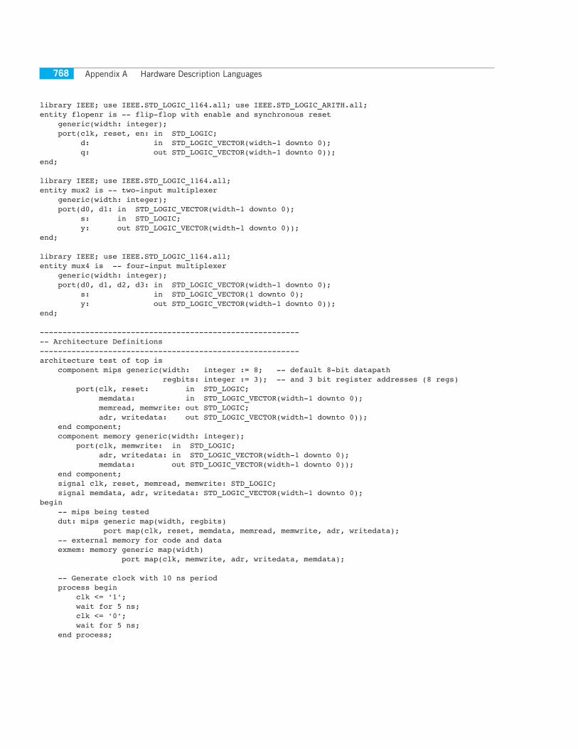
Appendix A Hardware Description Languages768
library IEEE; use IEEE.STD_LOGIC_1164.all; use IEEE.STD_LOGIC_ARITH.all;entity flopenr is -- flip-flop with enable and synchronous reset generic(width: integer); port(clk, reset, en: in STD_LOGIC; d: in STD_LOGIC_VECTOR(width-1 downto 0); q: out STD_LOGIC_VECTOR(width-1 downto 0));end;
library IEEE; use IEEE.STD_LOGIC_1164.all;entity mux2 is -- two-input multiplexer generic(width: integer); port(d0, d1: in STD_LOGIC_VECTOR(width-1 downto 0); s: in STD_LOGIC; y: out STD_LOGIC_VECTOR(width-1 downto 0));end;
library IEEE; use IEEE.STD_LOGIC_1164.all;entity mux4 is -- four-input multiplexer generic(width: integer); port(d0, d1, d2, d3: in STD_LOGIC_VECTOR(width-1 downto 0); s: in STD_LOGIC_VECTOR(1 downto 0); y: out STD_LOGIC_VECTOR(width-1 downto 0));end;
----------------------------------------------------------- Architecture Definitions---------------------------------------------------------architecture test of top is component mips generic(width: integer := 8; -- default 8-bit datapath regbits: integer := 3); -- and 3 bit register addresses (8 regs) port(clk, reset: in STD_LOGIC; memdata: in STD_LOGIC_VECTOR(width-1 downto 0); memread, memwrite: out STD_LOGIC; adr, writedata: out STD_LOGIC_VECTOR(width-1 downto 0)); end component; component memory generic(width: integer); port(clk, memwrite: in STD_LOGIC; adr, writedata: in STD_LOGIC_VECTOR(width-1 downto 0); memdata: out STD_LOGIC_VECTOR(width-1 downto 0)); end component; signal clk, reset, memread, memwrite: STD_LOGIC; signal memdata, adr, writedata: STD_LOGIC_VECTOR(width-1 downto 0);begin -- mips being tested dut: mips generic map(width, regbits) port map(clk, reset, memdata, memread, memwrite, adr, writedata); -- external memory for code and data exmem: memory generic map(width) port map(clk, memwrite, adr, writedata, memdata);
-- Generate clock with 10 ns period process begin clk <= '1'; wait for 5 ns; clk <= '0'; wait for 5 ns; end process;
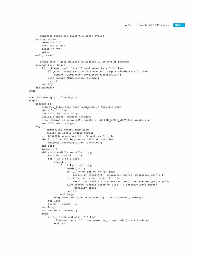
A.12 Example: MIPS Processor 769
-- Generate reset for first two clock cycles process begin reset <= '1'; wait for 22 ns; reset <= '0'; wait; end process;
-- check that 7 gets written to address 76 at end of program process (clk) begin if (clk'event and clk = '0' and memwrite = '1') then if (conv_integer(adr) = 76 and conv_integer(writedata) = 7) then report "Simulation completed successfully"; else report "Simulation failed."; end if; end if; end process;end;
architecture synth of memory isbegin process is file mem_file: text open read_mode is "memfile.dat"; variable L: line; variable ch: character; variable index, result: integer; type ramtype is array (255 downto 0) of STD_LOGIC_VECTOR(7 downto 0); variable mem: ramtype; begin
-- initialize memory from file-- memory in little-endian format-- 80020044 means mem[3] = 80 and mem[0] = 44
for i in 0 to 255 loop -- set all contents low mem(conv_integer(i)) := "00000000"; end loop; index := 0; while not endfile(mem_file) loop readline(mem_file, L); for j in 0 to 3 loop result := 0; for i in 1 to 2 loop read(L, ch); if '0' <= ch and ch <= '9' then result := result*16 + character'pos(ch)-character'pos('0'); elsif 'a' <= ch and ch <= 'f' then result := result*16 + character'pos(ch)-character'pos('a')+10; else report "Format error on line " & integer'image(index) severity error; end if; end loop; mem(index*4+3-j) := conv_std_logic_vector(result, width); end loop; index := index + 1; end loop; -- read or write memory loop if clk'event and clk = '1' then if (memwrite = '1') then mem(conv_integer(adr)) := writedata; end if;
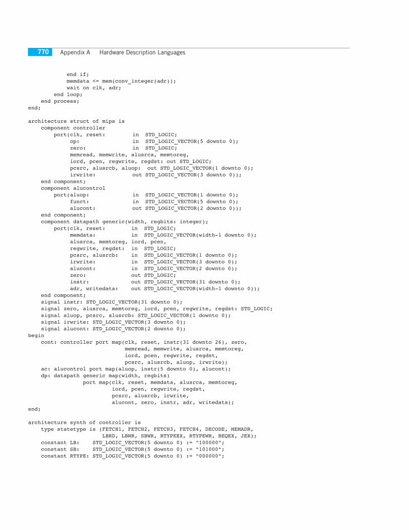
Appendix A Hardware Description Languages770
end if; memdata <= mem(conv_integer(adr)); wait on clk, adr; end loop; end process;end;
architecture struct of mips is component controller port(clk, reset: in STD_LOGIC; op: in STD_LOGIC_VECTOR(5 downto 0); zero: in STD_LOGIC; memread, memwrite, alusrca, memtoreg, iord, pcen, regwrite, regdst: out STD_LOGIC; pcsrc, alusrcb, aluop: out STD_LOGIC_VECTOR(1 downto 0); irwrite: out STD_LOGIC_VECTOR(3 downto 0)); end component; component alucontrol port(aluop: in STD_LOGIC_VECTOR(1 downto 0); funct: in STD_LOGIC_VECTOR(5 downto 0); alucont: out STD_LOGIC_VECTOR(2 downto 0)); end component; component datapath generic(width, regbits: integer); port(clk, reset: in STD_LOGIC; memdata: in STD_LOGIC_VECTOR(width-1 downto 0); alusrca, memtoreg, iord, pcen, regwrite, regdst: in STD_LOGIC; pcsrc, alusrcb: in STD_LOGIC_VECTOR(1 downto 0); irwrite: in STD_LOGIC_VECTOR(3 downto 0); alucont: in STD_LOGIC_VECTOR(2 downto 0); zero: out STD_LOGIC; instr: out STD_LOGIC_VECTOR(31 downto 0); adr, writedata: out STD_LOGIC_VECTOR(width-1 downto 0)); end component; signal instr: STD_LOGIC_VECTOR(31 downto 0); signal zero, alusrca, memtoreg, iord, pcen, regwrite, regdst: STD_LOGIC; signal aluop, pcsrc, alusrcb: STD_LOGIC_VECTOR(1 downto 0); signal irwrite: STD_LOGIC_VECTOR(3 downto 0); signal alucont: STD_LOGIC_VECTOR(2 downto 0);begin cont: controller port map(clk, reset, instr(31 downto 26), zero, memread, memwrite, alusrca, memtoreg, iord, pcen, regwrite, regdst, pcsrc, alusrcb, aluop, irwrite); ac: alucontrol port map(aluop, instr(5 downto 0), alucont); dp: datapath generic map(width, regbits) port map(clk, reset, memdata, alusrca, memtoreg, iord, pcen, regwrite, regdst, pcsrc, alusrcb, irwrite, alucont, zero, instr, adr, writedata);end;
architecture synth of controller is type statetype is (FETCH1, FETCH2, FETCH3, FETCH4, DECODE, MEMADR, LBRD, LBWR, SBWR, RTYPEEX, RTYPEWR, BEQEX, JEX); constant LB: STD_LOGIC_VECTOR(5 downto 0) := "100000"; constant SB: STD_LOGIC_VECTOR(5 downto 0) := "101000"; constant RTYPE: STD_LOGIC_VECTOR(5 downto 0) := "000000";
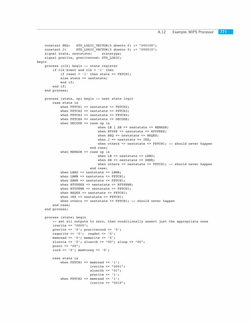
A.12 Example: MIPS Processor 771
constant BEQ: STD_LOGIC_VECTOR(5 downto 0) := "000100"; constant J: STD_LOGIC_VECTOR(5 downto 0) := "000010"; signal state, nextstate: statetype; signal pcwrite, pcwritecond: STD_LOGIC;begin process (clk) begin -- state register if clk'event and clk = '1' then if reset = '1' then state <= FETCH1; else state <= nextstate; end if; end if; end process;
process (state, op) begin -- next state logic case state is when FETCH1 => nextstate <= FETCH2; when FETCH2 => nextstate <= FETCH3; when FETCH3 => nextstate <= FETCH4; when FETCH4 => nextstate <= DECODE; when DECODE => case op is when LB | SB => nextstate <= MEMADR; when RTYPE => nextstate <= RTYPEEX; when BEQ => nextstate <= BEQEX; when J => nextstate <= JEX; when others => nextstate <= FETCH1; -- should never happen end case; when MEMADR => case op is when LB => nextstate <= LBRD; when SB => nextstate <= SBWR; when others => nextstate <= FETCH1; -- should never happen end case; when LBRD => nextstate <= LBWR; when LBWR => nextstate <= FETCH1; when SBWR => nextstate <= FETCH1; when RTYPEEX => nextstate <= RTYPEWR; when RTYPEWR => nextstate <= FETCH1; when BEQEX => nextstate <= FETCH1; when JEX => nextstate <= FETCH1; when others => nextstate <= FETCH1; -- should never happen end case; end process;
process (state) begin -- set all outputs to zero, then conditionally assert just the appropriate ones irwrite <= "0000"; pcwrite <= '0'; pcwritecond <= '0'; regwrite <= '0'; regdst <= '0'; memread <= '0'; memwrite <= '0'; alusrca <= '0'; alusrcb <= "00"; aluop <= "00"; pcsrc <= "00"; iord <= '0'; memtoreg <= '0';
case state is when FETCH1 => memread <= '1'; irwrite <= "0001"; alusrcb <= "01"; pcwrite <= '1'; when FETCH2 => memread <= '1'; irwrite <= "0010";
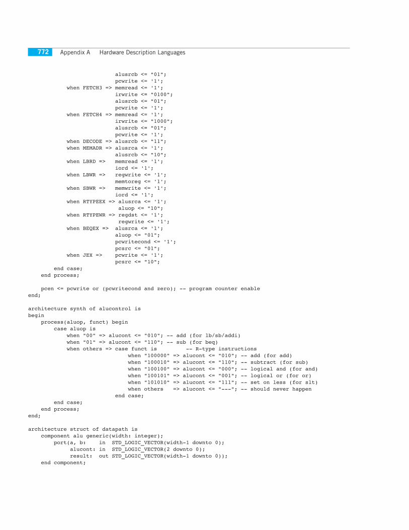
Appendix A Hardware Description Languages772
alusrcb <= "01"; pcwrite <= '1'; when FETCH3 => memread <= '1'; irwrite <= "0100"; alusrcb <= "01"; pcwrite <= '1'; when FETCH4 => memread <= '1'; irwrite <= "1000"; alusrcb <= "01"; pcwrite <= '1'; when DECODE => alusrcb <= "11"; when MEMADR => alusrca <= '1'; alusrcb <= "10"; when LBRD => memread <= '1'; iord <= '1'; when LBWR => regwrite <= '1'; memtoreg <= '1'; when SBWR => memwrite <= '1'; iord <= '1'; when RTYPEEX => alusrca <= '1'; aluop <= "10"; when RTYPEWR => regdst <= '1'; regwrite <= '1'; when BEQEX => alusrca <= '1'; aluop <= "01"; pcwritecond <= '1'; pcsrc <= "01"; when JEX => pcwrite <= '1'; pcsrc <= "10"; end case; end process;
pcen <= pcwrite or (pcwritecond and zero); -- program counter enableend;
architecture synth of alucontrol isbegin process(aluop, funct) begin case aluop is when "00" => alucont <= "010"; -- add (for lb/sb/addi) when "01" => alucont <= "110"; -- sub (for beq) when others => case funct is -- R-type instructions when "100000" => alucont <= "010"; -- add (for add) when "100010" => alucont <= "110"; -- subtract (for sub) when "100100" => alucont <= "000"; -- logical and (for and) when "100101" => alucont <= "001"; -- logical or (for or) when "101010" => alucont <= "111"; -- set on less (for slt) when others => alucont <= "---"; -- should never happen end case; end case; end process;end;
architecture struct of datapath is component alu generic(width: integer); port(a, b: in STD_LOGIC_VECTOR(width-1 downto 0); alucont: in STD_LOGIC_VECTOR(2 downto 0); result: out STD_LOGIC_VECTOR(width-1 downto 0)); end component;
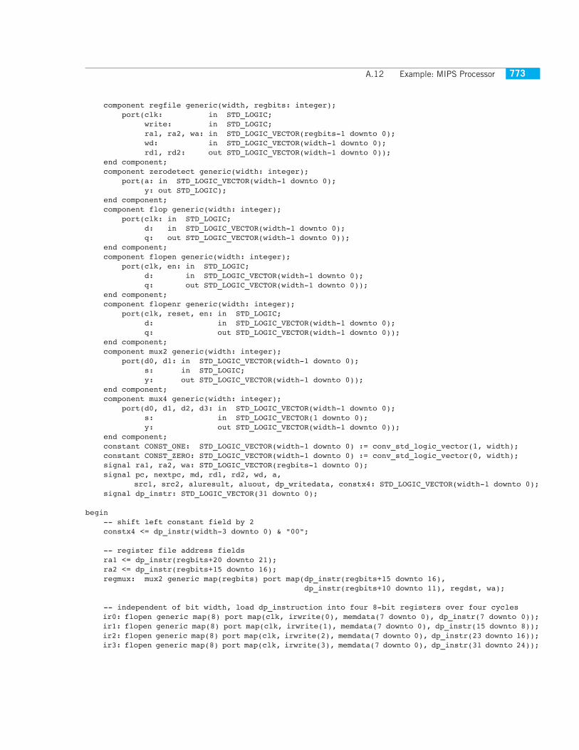
A.12 Example: MIPS Processor 773
component regfile generic(width, regbits: integer); port(clk: in STD_LOGIC; write: in STD_LOGIC; ra1, ra2, wa: in STD_LOGIC_VECTOR(regbits-1 downto 0); wd: in STD_LOGIC_VECTOR(width-1 downto 0); rd1, rd2: out STD_LOGIC_VECTOR(width-1 downto 0)); end component; component zerodetect generic(width: integer); port(a: in STD_LOGIC_VECTOR(width-1 downto 0); y: out STD_LOGIC); end component; component flop generic(width: integer); port(clk: in STD_LOGIC; d: in STD_LOGIC_VECTOR(width-1 downto 0); q: out STD_LOGIC_VECTOR(width-1 downto 0)); end component; component flopen generic(width: integer); port(clk, en: in STD_LOGIC; d: in STD_LOGIC_VECTOR(width-1 downto 0); q: out STD_LOGIC_VECTOR(width-1 downto 0)); end component; component flopenr generic(width: integer); port(clk, reset, en: in STD_LOGIC; d: in STD_LOGIC_VECTOR(width-1 downto 0); q: out STD_LOGIC_VECTOR(width-1 downto 0)); end component; component mux2 generic(width: integer); port(d0, d1: in STD_LOGIC_VECTOR(width-1 downto 0); s: in STD_LOGIC; y: out STD_LOGIC_VECTOR(width-1 downto 0)); end component; component mux4 generic(width: integer); port(d0, d1, d2, d3: in STD_LOGIC_VECTOR(width-1 downto 0); s: in STD_LOGIC_VECTOR(1 downto 0); y: out STD_LOGIC_VECTOR(width-1 downto 0)); end component; constant CONST_ONE: STD_LOGIC_VECTOR(width-1 downto 0) := conv_std_logic_vector(1, width); constant CONST_ZERO: STD_LOGIC_VECTOR(width-1 downto 0) := conv_std_logic_vector(0, width); signal ra1, ra2, wa: STD_LOGIC_VECTOR(regbits-1 downto 0); signal pc, nextpc, md, rd1, rd2, wd, a, src1, src2, aluresult, aluout, dp_writedata, constx4: STD_LOGIC_VECTOR(width-1 downto 0); signal dp_instr: STD_LOGIC_VECTOR(31 downto 0);
begin -- shift left constant field by 2 constx4 <= dp_instr(width-3 downto 0) & "00";
-- register file address fields ra1 <= dp_instr(regbits+20 downto 21); ra2 <= dp_instr(regbits+15 downto 16); regmux: mux2 generic map(regbits) port map(dp_instr(regbits+15 downto 16), dp_instr(regbits+10 downto 11), regdst, wa);
-- independent of bit width, load dp_instruction into four 8-bit registers over four cyclesir0: flopen generic map(8) port map(clk, irwrite(0), memdata(7 downto 0), dp_instr(7 downto 0));ir1: flopen generic map(8) port map(clk, irwrite(1), memdata(7 downto 0), dp_instr(15 downto 8));ir2: flopen generic map(8) port map(clk, irwrite(2), memdata(7 downto 0), dp_instr(23 downto 16));ir3: flopen generic map(8) port map(clk, irwrite(3), memdata(7 downto 0), dp_instr(31 downto 24));
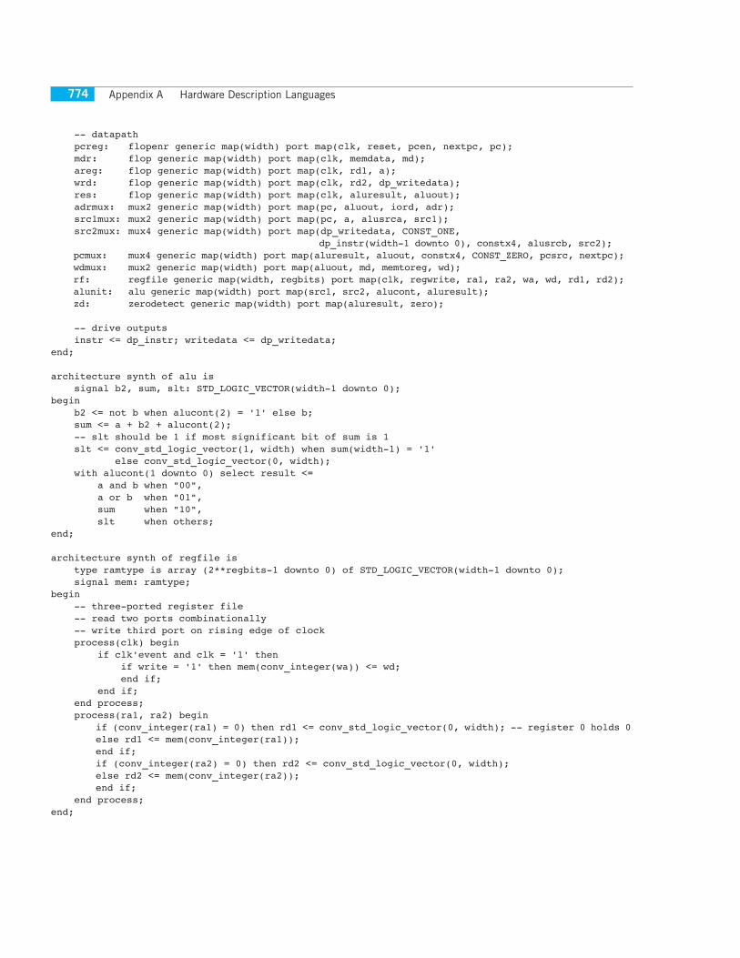
Appendix A Hardware Description Languages774
-- datapath pcreg: flopenr generic map(width) port map(clk, reset, pcen, nextpc, pc); mdr: flop generic map(width) port map(clk, memdata, md); areg: flop generic map(width) port map(clk, rd1, a); wrd: flop generic map(width) port map(clk, rd2, dp_writedata); res: flop generic map(width) port map(clk, aluresult, aluout); adrmux: mux2 generic map(width) port map(pc, aluout, iord, adr); src1mux: mux2 generic map(width) port map(pc, a, alusrca, src1); src2mux: mux4 generic map(width) port map(dp_writedata, CONST_ONE, dp_instr(width-1 downto 0), constx4, alusrcb, src2); pcmux: mux4 generic map(width) port map(aluresult, aluout, constx4, CONST_ZERO, pcsrc, nextpc); wdmux: mux2 generic map(width) port map(aluout, md, memtoreg, wd); rf: regfile generic map(width, regbits) port map(clk, regwrite, ra1, ra2, wa, wd, rd1, rd2); alunit: alu generic map(width) port map(src1, src2, alucont, aluresult); zd: zerodetect generic map(width) port map(aluresult, zero); -- drive outputs instr <= dp_instr; writedata <= dp_writedata;end;
architecture synth of alu is signal b2, sum, slt: STD_LOGIC_VECTOR(width-1 downto 0);begin b2 <= not b when alucont(2) = '1' else b; sum <= a + b2 + alucont(2); -- slt should be 1 if most significant bit of sum is 1 slt <= conv_std_logic_vector(1, width) when sum(width-1) = '1' else conv_std_logic_vector(0, width); with alucont(1 downto 0) select result <= a and b when "00", a or b when "01", sum when "10", slt when others;end;
architecture synth of regfile is type ramtype is array (2**regbits-1 downto 0) of STD_LOGIC_VECTOR(width-1 downto 0); signal mem: ramtype;begin -- three-ported register file -- read two ports combinationally -- write third port on rising edge of clock process(clk) begin if clk'event and clk = '1' then if write = '1' then mem(conv_integer(wa)) <= wd; end if; end if; end process; process(ra1, ra2) begin
if (conv_integer(ra1) = 0) then rd1 <= conv_std_logic_vector(0, width); -- register 0 holds 0else rd1 <= mem(conv_integer(ra1));end if;if (conv_integer(ra2) = 0) then rd2 <= conv_std_logic_vector(0, width); else rd2 <= mem(conv_integer(ra2));end if;
end process;end;
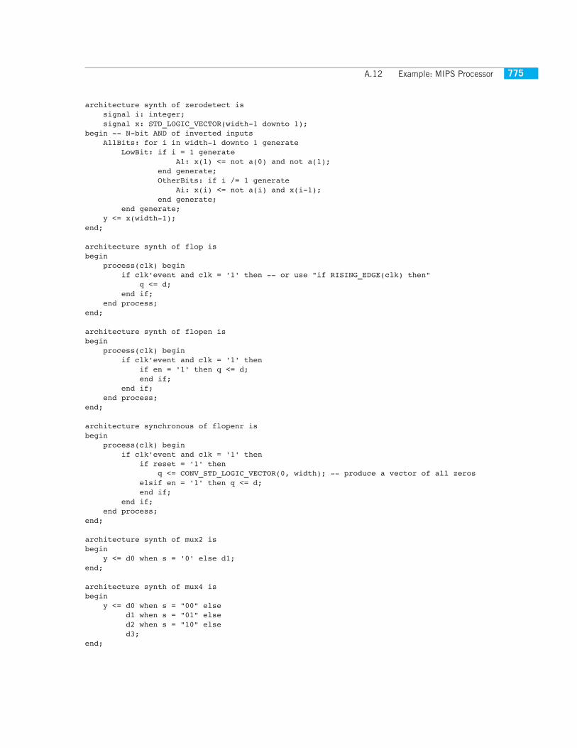
A.12 Example: MIPS Processor 775
architecture synth of zerodetect is signal i: integer; signal x: STD_LOGIC_VECTOR(width-1 downto 1);begin -- N-bit AND of inverted inputs AllBits: for i in width-1 downto 1 generate LowBit: if i = 1 generate A1: x(1) <= not a(0) and not a(1); end generate; OtherBits: if i /= 1 generate Ai: x(i) <= not a(i) and x(i-1); end generate; end generate; y <= x(width-1);end;
architecture synth of flop isbegin process(clk) begin if clk'event and clk = '1' then -- or use "if RISING_EDGE(clk) then" q <= d; end if; end process;end;
architecture synth of flopen isbegin process(clk) begin if clk'event and clk = '1' then if en = '1' then q <= d; end if; end if; end process;end;
architecture synchronous of flopenr isbegin process(clk) begin if clk'event and clk = '1' then if reset = '1' then q <= CONV_STD_LOGIC_VECTOR(0, width); -- produce a vector of all zeros elsif en = '1' then q <= d; end if; end if; end process;end;
architecture synth of mux2 isbegin y <= d0 when s = '0' else d1;end;
architecture synth of mux4 isbegin y <= d0 when s = "00" else d1 when s = "01" else d2 when s = "10" else d3;end;
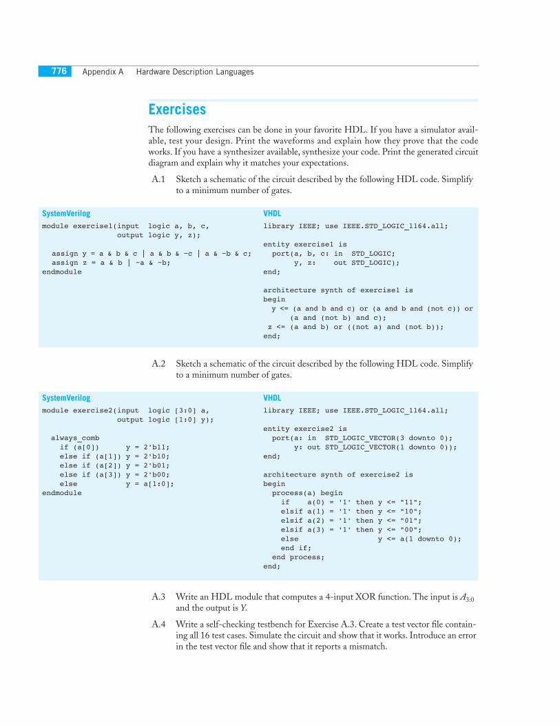
Appendix A Hardware Description Languages776
ExercisesThe following exercises can be done in your favorite HDL. If you have a simulator avail-able, test your design. Print the waveforms and explain how they prove that the codeworks. If you have a synthesizer available, synthesize your code. Print the generated circuitdiagram and explain why it matches your expectations.
A.1 Sketch a schematic of the circuit described by the following HDL code. Simplify to a minimum number of gates.
A.2 Sketch a schematic of the circuit described by the following HDL code. Simplify to a minimum number of gates.
A.3 Write an HDL module that computes a 4-input XOR function. The input is A3:0 and the output is Y.
A.4 Write a self-checking testbench for Exercise A.3. Create a test vector file contain-ing all 16 test cases. Simulate the circuit and show that it works. Introduce an error in the test vector file and show that it reports a mismatch.
SystemVerilog
module exercise1(input logic a, b, c, output logic y, z);
assign y = a & b & c | a & b & ~c | a & ~b & c;assign z = a & b | ~a & ~b;
endmodule
VHDL
library IEEE; use IEEE.STD_LOGIC_1164.all;
entity exercise1 is port(a, b, c: in STD_LOGIC; y, z: out STD_LOGIC);end;
architecture synth of exercise1 isbegin y <= (a and b and c) or (a and b and (not c)) or (a and (not b) and c); z <= (a and b) or ((not a) and (not b));end;
SystemVerilog
module exercise2(input logic [3:0] a, output logic [1:0] y); always_comb if (a[0]) y = 2'b11; else if (a[1]) y = 2'b10; else if (a[2]) y = 2'b01; else if (a[3]) y = 2'b00; else y = a[1:0];endmodule
VHDL
library IEEE; use IEEE.STD_LOGIC_1164.all;
entity exercise2 is port(a: in STD_LOGIC_VECTOR(3 downto 0); y: out STD_LOGIC_VECTOR(1 downto 0));end;
architecture synth of exercise2 isbegin process(a) begin if a(0) = '1' then y <= "11"; elsif a(1) = '1' then y <= "10"; elsif a(2) = '1' then y <= "01"; elsif a(3) = '1' then y <= "00"; else y <= a(1 downto 0); end if; end process;end;
Exercises 777
A.5 Write an HDL module called minority. It receives three inputs, A, B, and C. It produces one output Y that is TRUE if at least two of the inputs are FALSE.
A.6 Write an HDL module for a hexadecimal 7-segment display decoder. The decoder should handle the digits A, B, C, D, E, and F as well as 0–9.
A.7 Write a self-checking testbench for Exercise A.6. Create a test vector file contain-ing all 16 test cases. Simulate the circuit and show that it works. Introduce an error in the test vector file and show that it reports a mismatch.
A.8 Write an 8:1 multiplexer module called mux8 with inputs S2:0, D0, D1, D2, D3, D4, D5, D6, D7, and output Y.
A.9 Write a structural module to compute Y = AB + BC + ABC using multiplexer logic. Use the 8:1 multiplexer from Exercise A.8.
A.10 Repeat Exercise A.9 using a 4:1 multiplexer and as many NOT gates as you need.
A.11 Section A.5.4 pointed out that a synchronizer could be correctly described with blocking assignments if the assignments were given in the proper order. Think of another simple sequential circuit that cannot be correctly described with blocking assignments regardless of order.
A.12 Write an HDL module for an 8-input priority circuit.
A.13 Write an HDL module for a 2:4 decoder.
A.14 Write an HDL module for a 6:64 decoder using three of the 2:4 decoders from Exercise A.13 along with 64 3-input AND gates.
A.15 Sketch the state transition diagram for the FSM described by the following HDL code.
SystemVerilog
module fsm2(input logic clk, reset, input logic a, b, output logic y);
typedef enum logic [1:0] {S0, S1, S2, S3} statetype;
statetype state, nextstate;
always_ff @(posedge clk) if (reset) state <= S0; else state <= nextstate;
always_comb case (state) S0: if (a ^ b) nextstate = S1; else nextstate = S0; S1: if (a & b) nextstate = S2; else nextstate = S0; S2: if (a | b) nextstate = S3; else nextstate = S0; S3: if (a | b) nextstate = S3; else nextstate = S0; endcase
VHDL
library IEEE; use IEEE.STD_LOGIC_1164.all;
entity fsm2 is port(clk, reset: in STD_LOGIC; a, b: in STD_LOGIC; y: out STD_LOGIC);end;
architecture synth of fsm2 is type statetype is (S0, S1, S2, S3); signal state, nextstate: statetype;begin process(clk, reset) begin if reset = '1' then state <= S0; elsif clk'event and clk = '1' then state <= nextstate; end if; end process;
process (state, a, b) begin case state is when S0 => if (a xor b) = '1' then nextstate <= S1; else nextstate <= S0; end if; (continues)
Appendix A Hardware Description Languages778
A.16 Sketch the state transition diagram for the FSM described by the following HDL code. An FSM of this nature is used in a branch predictor on some microprocessors.
SystemVerilog (continued) assign y = (state == S1) || (state == S2);endmodule
VHDL (continued) when S1 => if (a and b) = '1' then nextstate <= S2; else nextstate <= S0; end if; when S2 => if (a or b) = '1' then nextstate <= S3; else nextstate <= S0; end if; when S3 => if (a or b) = '1' then nextstate <= S3; else nextstate <= S0; end if; end case; end process;
y <= '1' when ((state = S1) or (state = S2)) else '0';end;
SystemVerilog
module fsm1(input logic clk, reset, input logic taken, back, output logic predicttaken); typedef enum logic [4:0] {S0 = 5'b00001, S1 = 5'b00010, S2 = 5'b00100, S3 = 5'b001000, S4 = 5'b10000} statetype;
statetype state, nextstate;
always_ff @(posedge clk) if (reset) state <= S2; else state <= nextstate;
always_comb case (state) S0: if (taken) nextstate = S1; else nextstate = S0; S1: if (taken) nextstate = S2; else nextstate = S0; S2: if (taken) nextstate = S3; else nextstate = S1; S3: if (taken) nextstate = S4; else nextstate = S2; S4: if (taken) nextstate = S4; else nextstate = S3; default: nextstate = S2; endcase
VHDL
library IEEE; use IEEE.STD_LOGIC_1164.all;
entity fsm1 is port(clk, reset: in STD_LOGIC; taken, back: in STD_LOGIC; predicttaken: out STD_LOGIC);end;
architecture synth of fsm1 is type statetype is (S0, S1, S2, S3, S4); signal state, nextstate: statetype;begin process(clk, reset) begin if reset = '1' then state <= S2; elsif clk'event and clk = '1' then state <= nextstate; end if; end process;
process (state, taken) begin case state is when S0 => if taken = '1' then nextstate <= S1; else nextstate <= S0; end if; when S1 => if taken = '1' then nextstate <= S2; else nextstate <= S0; end if;
(continues)
Exercises 779
A.17 Write an HDL module for an SR latch.
A.18 Write an HDL module for a JK flip-flop. The flip-flop has inputs clk, J, and K, and output Q. On the rising edge of the clock, Q keeps its old value if J = K = 0. It sets Q to 1 if J = 1, resets Q to 0 if K = 1, and inverts Q if J = K = 1.
A.19 Write a line of HDL code that gates a 32-bit bus called data with another signal called sel to produce a 32-bit result. If sel is TRUE, result = data. Oth-erwise, result should be all 0s.
SystemVerilog ExercisesThe following exercises are specific to SystemVerilog.
A.20 Explain the difference between blocking and nonblocking assignments in SystemVerilog. Give examples.
A.21 What does the following SystemVerilog statement do?result = |(data[15:0] & 16'hC820);
A.22 Rewrite the syncbad module from Section A.5.4. Use nonblocking assignments, but change the code to produce a correct synchronizer with two flip-flops.
A.23 Consider the following two pieces of SystemVerilog code. Do they have the same function? Sketch the hardware each one implies.module code1(input logic clk, a, b, c, output logic y); logic x;
always_ff @(posedge clk) begin x <= a & b; y <= x | c; endendmodule
SystemVerilog (continued) assign predicttaken = (state == S4) || (state == S3) || (state == S2 && back);endmodule
VHDL (continued) when S2 => if taken = '1' then nextstate <= S3; else nextstate <= S1; end if; when S3 => if taken = '1' then nextstate <= S4; else nextstate <= S2; end if; when S4 => if taken = '1' then nextstate <= S4; else nextstate <= S3; end if; when others => nextstate <= S2; end case; end process;
-- output logic predicttaken <= '1' when ((state = S4) or (state = S3) or (state = S2 and back = '1')) else '0';end;
Appendix A Hardware Description Languages780
module code2(input logic a, b, c, clk, output logic y); logic x;
always_ff @(posedge clk) begin y <= x | c; x <= a & b; endendmodule
A.24 Repeat Exercise A.23 if the <= is replaced by = everywhere in the code.
A.25 The following SystemVerilog modules show errors that the authors have seen stu-dents make in the lab. Explain the error in each module and how to fix it.
module latch(input logic clk, input logic [3:0] d, output logic [3:0] q);
always @(clk) if (clk) q <= d;endmodule
module gates(input logic [3:0] a, b, output logic [3:0] y1, y2, y3, y4, y5);
always @(a) begin y1 = a & b; y2 = a | b; y3 = a ^ b; y4 = ~(a & b); y5 = ~(a | b); endendmodule
module mux2(input logic [3:0] d0, d1, input logic s, output logic [3:0] y); always @(posedge s) if (s) y <= d1; else y <= d0; endmodule
module twoflops(input logic clk, input logic d0, d1, output logic q0, q1);
always @(posedge clk) q1 = d1; q0 = d0;endmodule
module FSM(input logic clk, input logic a, output logic out1, out2);
logic state;
Exercises 781
// next state logic and register (sequential) always_ff @(posedge clk) if (state == 0) begin if (a) state <= 1; end else begin if (~a) state <= 0; end
always_comb // output logic (combinational) if (state == 0) out1 = 1; else out2 = 1;endmodule
module priority(input logic [3:0] a, output logic [3:0] y);
always_comb if (a[3]) y = 4'b1000; else if (a[2]) y = 4'b0100; else if (a[1]) y = 4'b0010; else if (a[0]) y = 4'b0001;endmodule
module divideby3FSM(input logic clk, input logic reset, output logic out);
typedef enum logic [1:0] {S0, S1, S2} statetype;
statetype state, nextstate;
// State Register always_ff @(posedge clk) if (reset) state <= S0; else state <= nextstate;
// Next State Logic always_comb case (state) S0: nextstate = S1; S1: nextstate = S2; S2: nextstate = S0; endcase
// Output Logic assign out = (state == S2);endmodule
module mux2tri(input logic [3:0] d0, d1, input logic s, output tri [3:0] y);
tristate t0(d0, s, y); tristate t1(d1, s, y);endmodule
module floprsen(input logic clk, input logic reset, input logic set,
Appendix A Hardware Description Languages782
input logic [3:0] d, output logic [3:0] q); always_ff @(posedge clk) if (reset) q <= 0; else q <= d;
always @(set) if (set) q <= 1;endmodule
module and3(input logic a, b, c, output logic y);
logic tmp;
always @(a, b, c) begin tmp <= a & b; y <= tmp & c; endendmodule
VHDL ExercisesThe following exercises are specific to VHDL.
A.26 In VHDL, why is it necessary to write
q <= '1' when state = S0 else '0';
rather than simply
q <= (state = S0); ?
A.27 Each of the following VHDL modules contains an error. For brevity, only the architecture is shown; assume the library use clause and entity declaration are cor-rect. Explain the error and how to fix it.
architecture synth of latch isbegin process(clk) begin if clk = '1' then q <= d; end if; end process;end;
architecture proc of gates isbegin process(a) begin y1 <= a and b; y2 <= a or b; y3 <= a xor b; y4 <= a nand b; y5 <= a nor b; end process;end;
architecture synth of flop is
Exercises 783
begin process(clk) if clk'event and clk = '1' then q <= d;end;
architecture synth of priority isbegin process(a) begin if a(3) = '1' then y <= "1000"; elsif a(2) = '1' then y <= "0100"; elsif a(1) = '1' then y <= "0010"; elsif a(0) = '1' then y <= "0001"; end if; end process;end;
architecture synth of divideby3FSM is type statetype is (S0, S1, S2); signal state, nextstate: statetype;begin process(clk, reset) begin if reset = '1' then state <= S0; elsif clk'event and clk = '1' then state <= nextstate; end if; end process;
process(state) begin case state is when S0 => nextstate <= S1; when S1 => nextstate <= S2; when S2 => nextstate <= S0; end case; end process;
q <= '1' when state = S0 else '0';end;
architecture struct of mux2 is component tristate port(a: in STD_LOGIC_VECTOR(3 downto 0); en: in STD_LOGIC; y: out STD_LOGIC_VECTOR(3 downto 0)); end component;begin t0: tristate port map(d0, s, y); t1: tristate port map(d1, s, y); end;
architecture asynchronous of flopr isbegin process(clk, reset) begin if reset = '1' then q <= '0'; elsif clk'event and clk = '1' then q <= d; end if; end process;
Appendix A Hardware Description Languages784
process(set) begin if set = '1' then q <= '1'; end if; end process;end;
architecture synth of mux3 isbegin y <= d2 when s(1) else d1 when s(0) else d0;end;