annual report - iap.uni-jena.de · verbesserung des kontrastverhältnisses von...
TRANSCRIPT

Annual Report

CONTENT
Institute of Applied Physics – Annual Report 2000
1
Imprint 2
Foreword 3
The Institute 5
· Research Profile
· Staff Members
Teaching 9
· Lectures
· Diploma Theses
· Doctoral Theses
Projects 11
· Statistics
· Externally Funded Projects
· Achievements and Results
Publications 47
· Journals
· Conference Contributions
· Patent Applications
Activities 55
· Fairs
· Convention
· Organizing Activities
Contact 57

IMPRINT
Institute of Applied Physics – Annual Report 2000
2
Publisher
Friedrich Schiller University Jena
Institute of Applied Physics
Max-Wien-Platz 1
D-07743 Jena
Germany
Authors
Prof. Dr. Andreas Tünnermann
Prof. Dr. Frank Wyrowski
Dr. Ernst-Bernhard Kley
Dr. Stefan Nolte
Dr. George Onishchukov
Dr. Jens-Peter Ruske
Dr. Holger Zellmer
© Institute of Applied Physics, Jena 2001 1

FOREWORD
Institute of Applied Physics – Annual Report 2000
3
This Annual Report details the activities of the Institute of Applied Physics (IAP) of the Friedrich
Schiller University Jena. It provides information on the people working at the IAP and gives a
summary of current research projects.
Two of the research highlights are the demonstration of fiber optical amplification of ultrashort
pulses up to energies of more than 100 µJ using the chirped pulse amplification technique, and
the demonstration of information transmission in optical fiber communication over distances up
to 28 000 km at high bit rates using soliton pulses (τp = 6 ps).
The past year was essentially characterized, on the one hand, by expansion due to the start of
new research projects, e. g. on the development of photonic crystals. The overall number of
scientists, technical personnel and students working at the IAP increased significantly, novel
equipment was installed. On the other hand, the year 2000 was characterized by limitations in
the daily work due to the reconstruction of the institute.
The institute during reconstruction.

FOREWORD
Institute of Applied Physics – Annual Report 2000
4
The research activities had been partially supported by the European Commission Directorate-
General XII: Science Research and Development, German Ministry of Education and Research,
German Research Foundation, Thuringian Ministry of Science, Research and Art and industrial
clients with a volume of almost 3 million €.
In the name of the entire staff of the IAP, I thank all of those who took interest in our work and
supported our institute in the past year.
Though adequate funding is a necessity, it does not suffice. The results and success of 2000,
described on the following pages, would not been achieved without the skills of our staff. I
thank all my colleagues for their hard and dedicated work in the past year, being confident that
the IAP is well prepared for the future. �
Jena, April 2001
Prof. Dr. Andreas Tünnermann
(Head of the Institute of Applied Physics)
THE INSTITUTE
Institute of Applied Physics – Annual Report 2000
5
The Institute of Applied Physics at the Friedrich Schiller University Jena has a longstanding
tradition and competence in design, fabrication and application of active and passive photonic
elements for both, optic and optoelectronic devices. A total staff of more than 30 scientists and
engineers is presently working in education and R&D. In addition, about 20 diploma and PhD
students and visiting scientists are researching at the IAP. Focal point of research is the
generation, control and amplification of spatially and/or temporally confined light.
The institute has a floor space of 1,200 m2 with installed clean rooms and optical laboratories
including microstructure technology (electron beam and photo lithogarphy, reactive ion and
reactive ion beam etching, diffusion and ion exchange ovens, coating facilities, scanning
electron and atomic force microscopy), optic/optoelectronic testing and measuring
instrumentation.
Research Profile
The Institute of Applied Physics at the Friedrich Schiller University Jena is engaged in the
development of:
· Advanced micro- and nano-processing technology
· All solid state lasers
· Amplitude and phase masks
· Calibration tools
· Electro-optical materials
· Fiber and waveguide lasers and amplifiers
· Integrated optical devices
· Microoptics (refractive/diffractive)
· Nonlinear optical devices
· Physical optical elements
· Ultrafast optics
THE INSTITUTE
Institute of Applied Physics – Annual Report 2000
6
Application fields are optical information and communication technology, medicine and biology,
process technology including material processing as well as optical measurement techniques.
These activities are partially supported by the European Commission Directorate-General XII:
Science, Research and Development, German Ministry of Education and Research, German
Research Foundation, and Thuringian Ministry of Science, Research and Art.
Staff Members
Abbe, Sylvia
Augustin, Markus
Bakonyi, Zoltan
Beeker, Christian
Bernhardt, Jens
Brüntjen, Thorsten
Chichkov, Boris N. Dr.
Clausnitzer, Tina
Cumme, Matthias
Drauschke, Andreas
Dubs, Carsten Dr.
Dürselen, Andrea
Erdmann, Tobias
Erler, Marco
Fuchs, Hans-Jörg Dr.
Gräf, Waltraud
Gründer, Hans-Georg
Grusemann, Ulrich
Häußler, Sieglinde
Hartung, Holger
Hartwig, Michael
THE INSTITUTE
Institute of Applied Physics – Annual Report 2000
7
Harzendorf, Torsten
Hermann, Andreas
Höfer, Sven
Hübner, Heike
Hübner, Uwe Dr.
Kästner, Tobias
Kley, Ernst-Bernhard Dr. Microstructure technology
Kölling, Kevin
Liem, Andreas
Limpert, Jens
Lührs, Hendrik Coordination office Optomatronik
Martin, Bodo
Matsushima, Kyoji Dr.
Nolte, Stefan Dr. Ultrafast optics
Okhrimchuk, Andrej Dr.
Onishchukov, George Dr.
Osipov, Vladimir Dr.
Otto, Christiane
Podorov, Sergej Dr.
Raubach, Sebastian
Riedel, Peter Dr.
Rockstroh, Sabine Secretary
Rockstroh, Werner
Rottschalk, Matthias Dr.
Ruske, Jens-Peter Dr. Integrated optics
Schelle, Detlef
Schimmel, Hagen

THE INSTITUTE
Institute of Applied Physics – Annual Report 2000
8
Schmeißer, Volkmar
Schmidt, Holger
Schnabel, Bernd
Steinberg, Carola
Steppa, Denny
Thieme, Mike
Thomas, Jens
Tünnermann, Andreas Prof. Dr. Head of the institute
Werner, Ekkehard
Will, Matthias
Wittig, Lars
Wyrowski, Frank Prof. Dr. Optical design
Zeitner, Brit
Zellmer, Holger Dr. Fiber and waveguide lasers
Zöllner, Karsten

TEACHING
Institute of Applied Physics – Annual Report 2000
9
Lectures
I. Summer Semester 2000
Prof. Dr. Frank Wyrowski
Optikdesign (Lecture)
Experimente im virtuellen Optiklabor (Seminar/practical course)
Ausgewählte Themen der Mikrooptik (Lecture)
Wellenoptisches Systemdesign (Seminar)
Prof. Dr. Andreas Tünnermann
Integrierte Optik (Lecture)
Experimentalphysik für Chemiker, Geowissen-
schaftler und Werkstoffwissenschaftler II (Lecture and seminars)
Institutsseminar (Seminar)
II. Winter Semester 2000/2001
Prof. Dr. Andreas Tünnermann
Festkörperlasertechnologie –
Grundlagen und Anwendung (Lecture)
Institutsseminar (Seminar)
Prof. Dr. Andreas Tünnermann, PD Dr. Boris Chichkov
Ausgewählte nichtlinear-optische Effekte bei der
Wechselwirkung von Laserstrahlung mit Materie (Seminar)
Prof. Dr. Andreas Tünnermann, PD Dr. Boris Chichkov,
Dr. Jens-Peter Ruske, Dr. Holger Zellmer
Nichtlinear-optische Effekte bei der Wechselwirkung
von Laserstrahlung mit Materie (Practical course)
TEACHING
Institute of Applied Physics – Annual Report 2000
10
Prof. Dr. Andreas Tünnermann, Dr. George Onishchukov
Faseroptische Datenübertragungssysteme (Lecture)
Prof. Dr. Frank Wyrowski
Experimente im virtuellen Labor (Practical course)
Wellenoptisches Systemdesign (Seminar)
Dr. Ernst-Bernhard Kley, Dr. Jens-Peter Ruske
Miniaturisierte Optik (Lecture)
Diploma Theses
Marco Erler: Untersuchung der physikalischen Eigenschaften integrierter Polarisatoren zur
Verbesserung des Kontrastverhältnisses von Intensitätsmodulatoren auf Basis von KTP
Torsten Harzendorf: Untersuchungen zu den Herstellungsmöglichkeiten glatter Höhenprofile für
mikrooptische Bauelemente
Ralph Kecke: Entwicklung und Realisierung eines aktiv modengekoppelten Faserlasers im
sichtbaren Spektralbereich
Doctoral Theses
Bernd Schnabel: Theorie und Fabrikation von Subwellenlängenstrukturen am Beispiel
polarisierender Metallstreifengitter

PROJECTS
Institute of Applied Physics – Annual Report 2000
11
Statistics
The research activities of the IAP are partially supported by the European Commission
Directorate-General XII: Science, Research and Development, German Ministry of Education
and Research (BMBF), German Research Foundation (DFG), Thuringian Ministry of Science,
Research and Art (TMWFK) and industrial clients with a budget of 2.7 million € (5.2 million DM).
Detail of an integrated-optical modulator –development funded by the TMWFK project „Integriert-optische Systemtechnik“.

PROJECTS
Institute of Applied Physics – Annual Report 2000
12
Externally Funded Projects
I. DFG Projects
(a) Nanostrukturierte photonische Komponenten und deren Wechselwirkung mit Licht
Runtime: April 2000 – March 2002
(b) Teilchenstrahl-stimulierte Ultrapräszisions-Oberflächenbearbeitung; TP Ionenätzen
Runtime: January 2000 – December 2001
(c) Brechzahlmodifikation in optisch transparenten Materialien durch
Strukturänderungen bei der Bestrahlung mit ultrakurzen Lichtpulsen; SFB TP B12
Runtime: January 1999 – December 2001
(d) Wellenoptisches Design monofunktionaler optischer Systeme
Runtime: August 2000 – July 2002
(e) Mikrooptische Funktionselemente – Innovationskolleg Optische
Informationstechnik, TP 3
Runtime: December 1994 – March 2000
(f) 3D- Wellenleiteroptik – Innovationskolleg Optische Informationstechnik, TP 4
Runtime: December 1994 – March 2000
(g) Nachrichtenübertragung mit Solitonen – Innovationskolleg Optische
Informationstechnik, TP 1
Runtime: December 1994 – April 2000
(h) Optische Übermittlungsverfahren in der Informationstechnik (DFG
Schwerpunktprogramm), Projekt: Sättigbare Absorber zur Rauschunterdrückung in
hochbitratigen optischen Übertragungsstrecken mit Halbleiterverstärkern
(in cooperation with Prof. Lederer, IFTO, Friedrich Schiller University Jena)

PROJECTS
Institute of Applied Physics – Annual Report 2000
13
II. TMWFK Projects
(a) Härtung und Strukturierung von Polymerschichten mit blauemittierenden Lasern
Runtime: October 1999 – September 2001
(b) Faserlaser im sichtbaren Spektralbereich für die medizinische Diagnostik –
FASIMED
Runtime: September 1998 – February 2000
(c) Intra-Netz Optomatronik
Runtime: January 2000 – December 2001
(d) Integriert-optische Systemtechnik: Herstellung und hybride Integration von aktiven
und passiven miniaturisierten optischen Elementen
Runtime: April 1999 – March 2002
(e) Integriert-optische Systemtechnik: Herstellung und hybride Integration von aktiven
und passiven miniaturisierten optischen Elementen – Investitionen
Runtime: March 1999 – December 2001
(f) Leistungsskalierung von Faserlasern im sichtbaren Spektralbereich für die
medizinische Therapie – LEFAMET
Runtime: October 1999 – December 2000
(g) Zentrum für Optomatronik – Realisierung von Optiklaboren
Runtime: May 2000 – December 2000
(h) Aufbau eines Technologielabors zur Untersuchung des Verstärkungsprozesses
ultrakurzer Pulse in dotierten Wellenleitern
Runtime: November 2000 – December 2000
PROJECTS
Institute of Applied Physics – Annual Report 2000
14
III. BMBF Projects
(a) Elekrooptischer Lasermikromodulator (MIKROMOD), TP: Integriert-optische
Modulatoren vom Mach-Zehnder-Interferometer
Runtime: October 1996 – March 2000
(b) Technologisch orientierte Untersuchungen zur Einführung geeigneter
Schichtsysteme zur Erzeugung minimaler Strukturabmessungen sowie
Belichtungen von SET-Bauelementen und Bauelementenarrays – Teil II (UA BMBF),
Runtime: July 1997 – June 2000
(c) Entwicklung und Musterfertigung von passiven mikrooptischen Komponenten für
ein DVD-Pick-up-System mit elektrooptischen Aktuatoren – NEOPICK (UA BMBF),
Runtime: October 1996 – June 2000
(d) Herstellung strukturierter Beleuchtungskomponenten für die EUV-Lithographie (UA
BMBF),
Runtime: May 2000 – April 2001
(e) Herstellung und Anwendung von Polarisationsgittern – SENTEX (UA BMBF),
Runtime: January 2000 – December 2001
(f) Diffraktive Kombinationsoptiken für Hochleistungsdiodenlaser (UA BMBF),
Runtime: October 1999 – December 2002
(g) Herstellung und Charakterisierung von Nano-Prägewerkzeugen und meßtechnische
Bewertung ihrer Replikate; Schwerpunkt: Hohe Aspektverhältnisse – FOKEN,
Runtime: July 2000 – June 2002
(h) MICROPHOT – Laserdirect: Faseroptische Hochleistungslaser für die
Druckvorstufe; Teilvorhaben: Neuartige Skalierungskonzepte für Faserlaser und
PROJECTS
Institute of Applied Physics – Annual Report 2000
15
-verstärker in kontinuierlichem und gepulstem Betrieb
Runtime: July 2000 – June 2003
(i) MICROPHOT – OMP: Integriert-optische Modulationskonzepte im sichtbaren
Spektralbereich
Runtime: July 2000 – June 2003
(j) Verbundprojekt Kompetenznetze Optische Technologien (Phase 2) im TV
Kompetenznetz OptoNet
Runtime: November 2000 – January 2001
(k) Grundlegende Untersuchungen zur Materialbearbeitung sowie die Berechnung und
Erprobung optischer Elemente zur Strahlformung ultrakurzer Laserpulse
Runtime: May 2000 – September 2002
(l) Laserstrahlformung mit Hilfe spezieller optischer Elemente
Runtime: May 2000 – September 2002
IV. EU Projects
(a) Nano-Fabrication of DFB-Lasers and SAW-Devices by Off-Axis Holographic
Lithography – SAWLASE, BriteEuram,
Runtime: October 1998 – September 2000
(b) Development of New Dielectric and Optical Materials and Process Technologies for
Low Cost Electrical and/or Optical Packaging and Testing of Precompetitive
Demonstrators – DONDODEM, BriteEuram,
Runtime: September 1998 – August 2001
(c) Semiconductor devices for optical signal processing – COST 267
(in cooperation with Prof. Lederer, IFTO, Friedrich-Schiller University Jena)
PROJECTS
Institute of Applied Physics – Annual Report 2000
16
Achievements and Results
I. Optical fiber communication systems Dr. George Onishchukov
The research in the field of optical fiber communication systems at the IAP is focused on the
investigation of performance of high bit-rate optical fiber communication systems based on
soliton transmission. The emphasis is placed on the study of physical processes limiting the
transmission distance in a re-circulating fiber loop setup. During the period of the report, the
research has concentrated on the specific features of two system types: one with in-line
semiconductor optical amplifiers and saturable absorbers, the other one with distributed Raman
fiber amplifiers.
Saturable absorbers in systems with semiconductor optical amplifiers
Semiconductor optical amplifiers (SOA) are very promising elements of integrated lightwave
circuits for optical fiber communication systems. It has been previously shown by the group
that Return-to-Zero (RZ) transmission systems with in-line SOA suffer from the fast signal
decay and growth of amplified spontaneous emission (ASE) because of the low saturation
energy and short recovery time of the SOA. It has been proposed and demonstrated that when
using in-line saturable absorbers (SA), it is possible to completely suppress ASE growth and
increase the maximum transmission distance many times – up to 30 000 km for 5 Gbit/s. The
limiting feature in that system is the SOA gain recovery causing bit rate dependent amplitude
pattern and temporal walk off effects and setting the limit on the maximum bit rate in the
system. One possibility to speed up the gain recovery and to reduce harmful effects is to use
the gain-clamped SOA design. Such a SOA prototype was purchased from JDS-Uniphase
(Netherlands). The dynamics of the gain recovery in the SOA has been studied in a pump-probe
setup. Characteristic features of strongly dumped relaxation oscillations have been found. The
dependence of the gain recovery on the operating parameters like pump current and
temperature has been investigated. Finally using the gain-clamped SOA after appropriate

PROJECTS
Institute of Applied Physics – Annual Report 2000
17
adjustment of its operation conditions it was possible to compensate for the dynamics of gain
recovery in the common SOA part of the SOA-SA module in the setup scheme shown in fig.1.
The 10 Gbit/s transmission over 5 000 km was demonstrated (fig.2). The results together with
previously obtained ones are the world longest transmission distances realized in the system
with in-line SOA.
Modulator
10Gbit/s DataECML-Laser
10GHz τ=20ps SOA
Fiber~25kmëzd=1306.14nm
GC-SOA90/10
80/20
Filter3nm
Filter0.9nm
SA SOA
Slowphotodiode
10Gb/s Receiver90/10
Spectrum Analyzer
Att.
Fig.1 System with in-line gain-clamped SOA and SA.
Fig.2 Eye-diagram at 5 000 km.

PROJECTS
Institute of Applied Physics – Annual Report 2000
18
From fundamental point of view, the optical fiber transmission line with in-line SOA and SA
represents an essentially nonlinear, strongly dissipative system, where the parameters of the
pulses (autosolitons) are completely determined by the system parameters. In contrast to
common soliton systems, the autosoliton parameters are independent of the initial pulse
duration, wavelength, and energy, and this feature has been proved in our experiments. It has
been also shown that such a system with two competing noninstantaneous nonlinearities (SOA
and SA) could have a new type of bifurcation behavior for a certain set of element parameters
as shown in fig.3. Its specific is that for supercritical bifurcation of CW radiation the bifurcation
of the solitons is subcritical. In the region of negative linear net gain, there are only two stable
solutions – trivial zero background and autosolitons. It is in contrast to the other well known
nonlinear systems where the bifurcation behavior of the CW radiation and of solitons have the
same features – either both supercritical or both subcritical. Dynamics of the system have been
also studied: switching of autosolitons and their relaxation. The effect of slowing down of the
relaxation, which is typical for nonlinear systems, has been demonstrated (fig.4).
linear net gain
amplitude
CW
soliton
Fig.3 Bifurcation diagram of dissipative solitons in system with competing noninstantaneous nonlinearities.

PROJECTS
Institute of Applied Physics – Annual Report 2000
19
Timing jitter is another performance limiting parameter of a transmission system and important
for applications. The investigation of the effect has been started and it has been shown that
very low (2 ps at 30 000 km) timing jitter could be obtained in the system. The unique features
of the system with in-line SOA-SA which are responsible for it are the following: On the one
hand, the system can operate at zero fiber dispersion with non-vanishing pulse energy as in
popular up-to-date systems with dispersion management. On the other hand, the effect of in-
line SA is that a strong in-line spectral filtering can be used without transmission deterioration.
These two features provide a very strong suppression of the timing jitter, due to the Gordon-
Haus effect, which is the main source of timing jitter in soliton systems.
Distributed Raman amplification
Raman fiber amplifiers are also among the most promising candidates for 1.3 – 1.6 µm
amplification because of their flexibility regarding the operation wavelength. Another attractive
feature of Raman amplification for high bite-rate soliton transmission is that it provides a
solitons
ASE
-0.12 -0.08 -0.04 0.00Iinear net gain
-15
-10
-5
Rela
xation c
onst
ant
(1/M
m)
Fig.4 Dependence of relaxation constant for dissipative solitons and amplified spontaneous emission on net gain.
PROJECTS
Institute of Applied Physics – Annual Report 2000
20
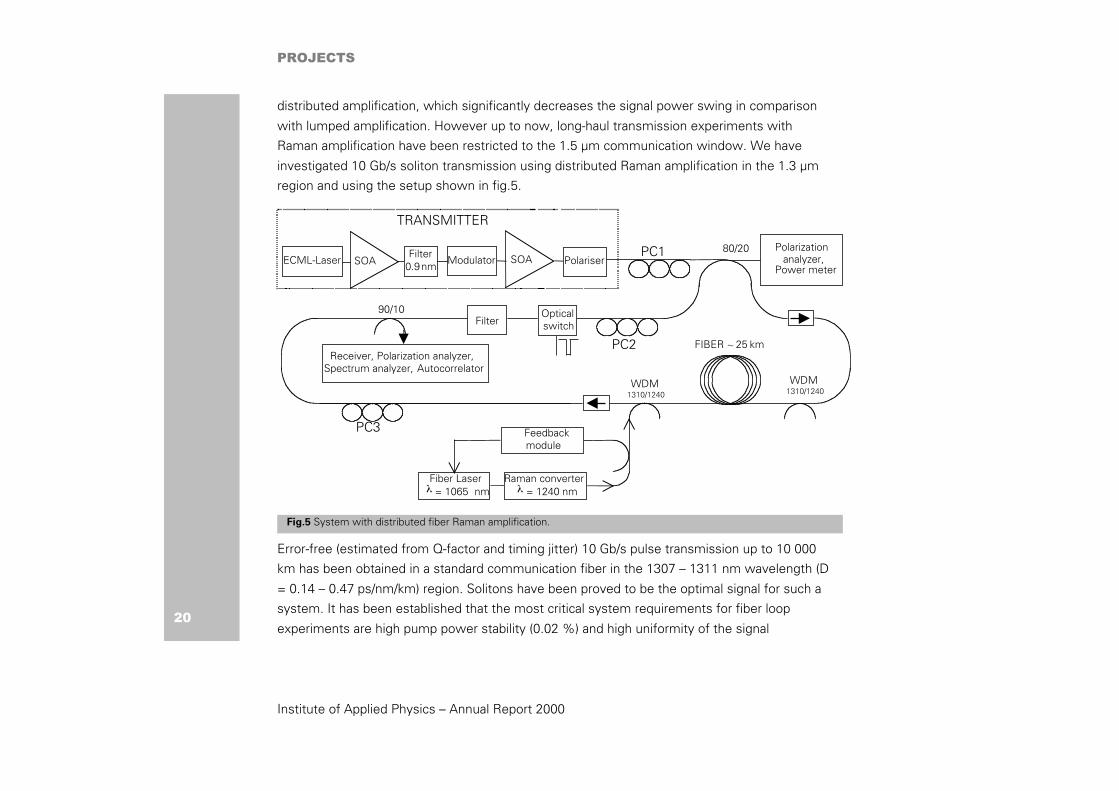
distributed amplification, which significantly decreases the signal power swing in comparison
with lumped amplification. However up to now, long-haul transmission experiments with
Raman amplification have been restricted to the 1.5 µm communication window. We have
investigated 10 Gb/s soliton transmission using distributed Raman amplification in the 1.3 µm
region and using the setup shown in fig.5.
Error-free (estimated from Q-factor and timing jitter) 10 Gb/s pulse transmission up to 10 000
km has been obtained in a standard communication fiber in the 1307 – 1311 nm wavelength (D
= 0.14 – 0.47 ps/nm/km) region. Solitons have been proved to be the optimal signal for such a
system. It has been established that the most critical system requirements for fiber loop
experiments are high pump power stability (0.02 %) and high uniformity of the signal
Polarization analyzer,
Power meter
FIBER ~ 25 km
80/20
WDM1310/1240
Opticalswitch
90/10
ModulatorECML-Laser SOAFilter0.9nmSOA Polariser
TRANSMITTER
Filter
Feedbackmodule
Raman converterλ = 1240 nm
Fiber Laserλ = 1065 nm
WDM1310/1240
Receiver, Polarization analyzer,Spectrum analyzer, Autocorrelator
PC3
PC1
PC2
Fig.5 System with distributed fiber Raman amplification.
PROJECTS
Institute of Applied Physics – Annual Report 2000
21
polarization state. We verified that dispersive waves generated by PMD are detrimental for
soliton transmission, but they can be minimized by implementation of an element with
polarization dependent transmittance and a proper adjustment of the signal polarization state. It
has been found that the polarization hole burning could be a detrimental effect for distributed
Raman amplification in fibers with low PMD. The fundamental limiting factor for long-haul
transmission, provided that the PMD effect is reduced, is the timing jitter due to spontaneous
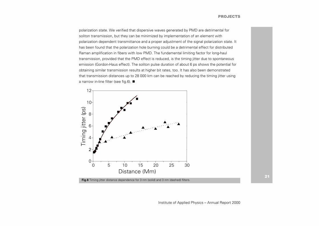
emission (Gordon-Haus effect). The soliton pulse duration of about 6 ps shows the potential for
obtaining similar transmission results at higher bit rates, too. It has also been demonstrated
that transmission distances up to 28 000 km can be reached by reducing the timing jitter using
a narrow in-line filter (see fig.6). �
0 5 10 15 20 25 300
2
4
6
8
10
12
Tim
ing
jitte
r (ps
)
Distance (Mm)Fig.6 Timing jitter distance dependence for 3 nm (solid) and 3 nm (dashed) filters.

PROJECTS
Institute of Applied Physics – Annual Report 2000
22
II. High average power ultrafast fiber CPA system Dr. Holger Zellmer
The field of fiber lasers and amplifiers is one of the main research areas of the IAP. Subjects are
up-conversion lasers with emission wavelengths in the visible spectral range and near infrared
double clad fiber lasers. The demonstration of a fiber CPA laser system for applications in
medicine and micro machining is the most promising result in this field.
Fiber laser CPA system
Today, regenerative amplifiers using chirped pulse amplification technique (CPA) are generally
applied to realize these parameters with repetition rates of up to 10 kHz. Higher repetition rates
can be achieved by applying the CPA technique to fiber amplifiers. Neodymium and ytterbium-
doped fibers can provide broad gain bandwidths (> 50 nm), optical pumping efficiencies as high
as 80% and high optical gain and power. Using double-clad fiber designs, cw powers in a nearly
single spatial mode beam of several 10 W have been reported for diode pumped systems.
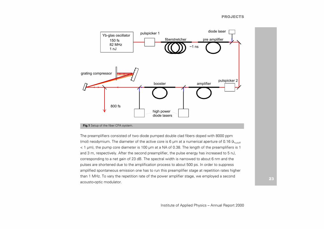
The experimental setup of our high-energy fiber CPA system is shown in fig. 1. The system
consists of a passively mode-locked, diode-pumped solid-state laser system, a fiber stretcher,
two single-mode neodymium-doped fiber preamplifiers, two ytterbium-doped fiber power
amplifiers and a diffraction-grating compressor. As a femtosecond seed source, a Nd:glass
laser system is applied which is based on a semiconductor saturable absorber mirror (SESAM).
The laser is running at 82 MHz repetition rate producing pulses as short as 150 fs at ~1060 nm
and an average power of 100 mW. After adjusting the repetition rate of the seed pulses in a
first acousto-optic modulator (AOM I) to 2 MHz, about 25 pJ pulse energy was coupled into a
dispersive delay line consisting of a 2000 m long step-index single-mode fiber which stretched
the pulses to a width of about 800 ps. The broadened spectrum (∆λ = 9.9 nm), compared with
the transform limited spectrum of the Nd:glass oscillator (∆λ = 6.9 nm), is due to inherent self
phase modulation in the 2 km long stretcher fiber.
PROJECTS
Institute of Applied Physics – Annual Report 2000
23
The preamplifiers consisted of two diode pumped double clad fibers doped with 8000 ppm
(mol) neodymium. The diameter of the active core is 6 µm at a numerical aperture of 0.16 (λcutoff
< 1 µm), the pump core diameter is 100 µm at a NA of 0.38. The length of the preamplifiers is 1
and 3 m, respectively. After the second preamplifier, the pulse energy has increased to 5 nJ,
corresponding to a net gain of 23 dB. The spectral width is narrowed to about 6 nm and the
pulses are shortened due to the amplification process to about 500 ps. In order to suppress
amplified spontaneous emission one has to run this preamplifier stage at repetition rates higher
than 1 MHz. To vary the repetition rate of the power amplifier stage, we employed a second
acousto-optic modulator.
Yb-glas oscillatorpulspicker 1
pre amplifierfiberstretcher
amplifierboosterpulspicker 2
150 fs82 MHz1 nJ
~1 ns
800 fs
diode laser
high powerdiode lasers
grating compressor
Fig.1 Setup of the fiber CPA system.
PROJECTS
Institute of Applied Physics – Annual Report 2000
24
The first power amplifier is using a 10 m long ytterbium-doped double clad fiber, fabricated by
IPHT Jena. A fiber coupled diode laser delivering 45 W at 940 nm is employed as pump source.
The diameters of the active core and the D-shaped pump core are 11 µm (NA = 0.16) and
400 µm (NA = 0.38), respectively. The ytterbium doping concentration is 6500 ppm (mol).
When seeded with 1.5 nJ at a repetition rate of 2 MHz, we were able to generate average
powers up to 4.6 W of amplified pulses with a launched pump power of 20 W. In this case, the
slope efficiency yields to 32%. Reducing the repetition rate of AOM II to 32 kHz, an average
power as high as 3.2 W could be reached, resulting in pulse energies of 100 µJ without any
significant changes in intensity spectrum. The amplified pulse spectrum at 32 kHz is shown in
fig. 3. The beam profile of the amplified pulses is nearly diffraction limited with a M2 ~ 1.7.
The stretched and amplified pulses were compressed using a conventional diffraction-grating
compressor. In order to demonstrate the possibility of compression of the generated 100 µJ
pulses, we picked up a fraction of the amplifier output with a single-mode fiber and sent it
through a pair of 1200 l/mm gratings. Even though we used no polarization maintaining fibers,
the efficiency of the compressor in a double pass is 25%. Best compression was found at a
grating separation of ~ 530 cm. The autocorrelation trace of 850 fs compressed pulses which
were picked up just after the 11 µm power amplifier is shown in fig. 4. The pulse duration is
limited, due to third order dispersion effects of the fiber stretcher, which cannot be
compensated by a grating compressor.
The second power amplifier consisted of 3 m of fiber with a 50 µm diameter, 0.16-NA
ytterbium-doped core, a 400 µm D-shaped inner cladding with NA = 0.38, and a polymer outer
cladding. When seeded with 1.7 µJ at a repetition rate of 2 MHz, we were able to produce
average powers up to 22 W of amplified pulses with a launched pump power of 50 W. The
slope efficiency of the last amplifier stage is as high as 52%. Reducing the repetition rate of
AOM II to 128 kHz, the pulse energies could be increased up to 130 µJ, i.e. an average power
of 16.5 W. A smooth beam profile was observed, emerging the last power amplifier with a M2

PROJECTS
Institute of Applied Physics – Annual Report 2000
25
~ 7. The compression of the emitted pulses to few ps is possible, but we observed a strongly
modulated autocorrelation trace with broad wings due to interference between guided modes.
0 5 10 15 200
1
2
3
4
5
slope efficiency = 32%
Ou
tpu
t p
ow
er [
W]
Launched pump power [W]
-5 0 50.0
0.2
0.4
0.6
0.8
1.0
∆∆∆∆ττττ FWHM = 850 fs
Inte
nsi
ty [
a.u
.]
Time [ps]
Fig.2 Slope of the first power amplifier operating at 2 MHz repetition rate.
Fig.3 Autocorrelation trace of recompressed pulses after first power amplifier.

PROJECTS
Institute of Applied Physics – Annual Report 2000
26
In conclusion, we have demonstrated the potential of high-gain Yb-doped fiber amplifier
systems to provide ultrashort pulses with average powers in excess of 20 W and energies of
more than 100 µJ. Investigations to further increase the pulse energy to more than 1 mJ are
presently under progress in collaboration with the Max Born Institute Berlin and the Institute for
Physical High Technology Jena. �
III. Wave-Optical Engineering Prof. Dr. Frank Wyrowski
The investigation of the wave nature of light in the analysis and the design of optical systems
constitutes one basic subject of the research and development of the institute.
Subject of wave-optical engineering
In contemporary optical systems design, ray tracing, which has its basis in geometrical optics,
is the employed standard tool. Through the use of modern computer technology, ray tracing
has become an extremely powerful technique in the design of both imaging and lighting
systems. Indeed, the success of ray-tracing methods has led many optical systems designers
to rely fully on ray tracing. Yet there are several reasons in modern optical engineering, which
require access to a wave-optical field representation of light. One exemplary situation is the
propagation through miniaturized or micro-structured optical systems and components. The
development of optical systems with novel functionalities often rely on merit functions which
are defined via the field representation of light. The light coupling efficiency into a fiber is an
example of such a merit function. In addition, modern optical design concepts, like amplitude
matching, require a field representation of light.
Optical system’s design that takes to some extent the wave nature of light into consideration is
appropriately called wave-optical engineering or physical-optics system design. This modern
field in optical design actually gains momentum to obtain innovative optical solutions.
Wave-optical engineering deals with the modeling of sources, the analysis and modeling of
linear interaction of light with inhomogeneous media, and the development of strategies, which

PROJECTS
Institute of Applied Physics – Annual Report 2000
27
allow the design of systems that perform a desired optical function. One example of our
research activities is briefly described in the following.
Example: High-resolution proximity printing by wave-optically designed masks
Proximity printing is a high throughput and cost effective lithographic technique for production
of e.g. large area flat panel displays. The resolution of this technique, however, is limited due to
diffraction effects that occur at mask pattern edges. We can improve the resolution drastically
by replacing the conventional photomask with a mask, which compensates these diffraction
effects. The resulting mask modulates phase and amplitude of the exposure beam in such a
way that the required image is formed at a predetermined distance behind the mask. This
research project was based on a cooperation between the Institute of Applied Physics, the
LightTrans GmbH in Jena, and Philips CFT in The Netherlands. The masks that have been
examined are designed to form an image at a distance of 50 micron behind the mask. The
mask contains 2 amplitude and 4 phase levels, and the pixel size is 1 micron. Under these
conditions, a 3-micron line/space pattern is clearly resolved, whereas under conventional
conditions the image is completely distorted.
Photomask
Collimated UV beam
Substrate with photoresist
Proximity gap
Fig.1 Schematic representation of proximity printing and layout of the photomask and target pattern used in thisstudy. The line width in the target pattern is 3 microns.

PROJECTS
Institute of Applied Physics – Annual Report 2000
28
Fig. 1 illustrates the basic subject of consideration. In the conventional technology, a mask is
applied in which the transmission is proportional to the goal light distribution, that is for
instance the target pattern in fig. 1. Then, the intensity and resist transmission shown in fig. 2
results. Obviously, the details of the target pattern are not resolved but destroyed by diffraction
effects.
On the basis of wave-optical design methods, we calculated a mask with 2 amplitude
transmission values (0 and 1) and 4 phase transmission values (0, 90, 180, and 270 degrees).
This mask was fabricated by using the Leica e-beam writer ZBA 23 H and etching technique by
structuring a chromium layer, which realizes the binary amplitude transmission and a four level
surface profile in fused silica, which generates the desired phase transmission. A SEM
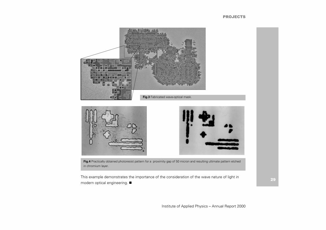
photograph of the resulting mask is depicted in fig. 3.
This mask was used in an optical experiment and the result is shown in fig. 4. Obviously, the 3-
micron line/space pattern is now clearly resolved.
Fig.2 Calculated intensity distribution (left) 50 micron behind the photomask as defined in figure 1 (right) and (right)the practically obtained corresponding photoresist profile.
PROJECTS
Institute of Applied Physics – Annual Report 2000
29This example demonstrates the importance of the consideration of the wave nature of light in
modern optical engineering. �
Fig.3 Fabricated wave-optical mask.
Fig.4 Practically obtained photoresist pattern for a proximity gap of 50 micron and resulting ultimate pattern etchedin chromium layer.

PROJECTS
Institute of Applied Physics – Annual Report 2000
30
IV. Micro- and nano-optical devices Dr. Ernst-Bernhard Kley
At the Institute of Applied Physics, investigations are performed in order to realize micro- and
nano-structured surfaces with complex optical functions. This includes design, manufacturing,
and characterization. One activity is related to the development of micro-optics for holography.
Here, a main problem is the unsatisfying low productivity because of the low exploitation of the
laser power that is used for the recording. This is caused by the expanding of the beam that is
necessary for getting a uniform intensity distribution in the central beam area in the recording
plane. To overcome this problem all the intensity of the beam should be converted into a top-
hat intensity distribution that is well adapted to the recording area. It is well known that beam
shaping elements can do this conversion [1–3], but such elements usually generate a wave
front aberration which can not be accepted for holography. In addition, such elements show
unacceptable wavelength aberrations if they are realized as diffractive ones. Therefore, basic
considerations as well as test experiments are necessary to realize a high efficient full color
holography.
Basic Considerations
The holographic recording of a lens function that can be realized with a typical well-known
setup is one aim of the present work. As the lens aperture is rectangular (quadratic) and all the
laser power should be used for the recording of the hologram, we need to concentrate the
recording beams into a uniform illuminated field adapted to this aperture. Different kinds of
beam shaping elements can make the conversion into such a top-hat or super Gaussian
distribution, but for its application in holography we meet the following demands:
· Low wave front distortion for getting a satisfying interference pattern,
· high conversion efficiency for an effective use of the laser power,
· low wavelength aberration, this could offer the use of the elements in the whole visible range,
· large depth of sharpness for getting a large alignment tolerance.
PROJECTS
Institute of Applied Physics – Annual Report 2000
31
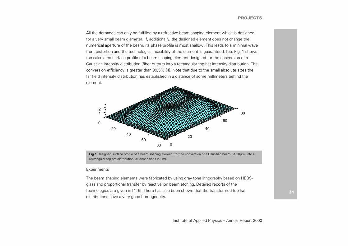
All the demands can only be fulfilled by a refractive beam shaping element which is designed
for a very small beam diameter. If, additionally, the designed element does not change the
numerical aperture of the beam, its phase profile is most shallow. This leads to a minimal wave
front distortion and the technological feasibility of the element is guaranteed, too. Fig. 1 shows
the calculated surface profile of a beam shaping element designed for the conversion of a
Gaussian intensity distribution (fiber output) into a rectangular top-hat intensity distribution. The
conversion efficiency is greater than 99,5% [4]. Note that due to the small absolute sizes the
far field intensity distribution has established in a distance of some millimeters behind the
element.
Experiments
The beam shaping elements were fabricated by using gray tone lithography based on HEBS-
glass and proportional transfer by reactive ion beam etching. Detailed reports of the
technologies are given in [4, 5]. There has also been shown that the transformed top-hat
distributions have a very good homogeneity.
0
20
40
6080 0
20
40
60
8012
Fig.1 Designed surface profile of a beam shaping element for the conversion of a Gaussian beam (∅ 20µm) into arectangular top-hat distribution (all dimensions in µm).
PROJECTS
Institute of Applied Physics – Annual Report 2000
32
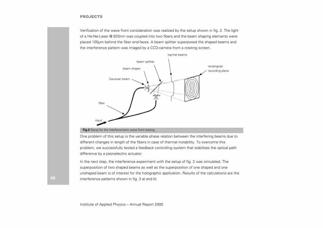
Verification of the wave front consideration was realized by the setup shown in fig. 2. The light
of a He-Ne-Laser @ 633nm was coupled into two fibers and the beam shaping elements were
placed 100µm behind the fiber end-faces. A beam splitter superposed the shaped beams and
the interference pattern was imaged by a CCD-camera from a rotating screen.
One problem of this setup is the variable phase relation between the interfering beams due to
different changes in length of the fibers in case of thermal instability. To overcome this
problem, we successfully tested a feedback controlling system that stabilizes the optical path
difference by a piezoelectric actuator.
In the next step, the interference experiment with the setup of fig. 2 was simulated. The
superposition of two shaped beams as well as the superposition of one shaped and one
unshaped beam is of interest for the holographic application. Results of the calculations are the
interference patterns shown in fig. 3 a) and b).
Fig.2 Setup for the interferometric wave front testing.
input
fiber
Gaussian beam
beam shaper
beam splitter
top-hat beams
rectangularrecording plane

PROJECTS
Institute of Applied Physics – Annual Report 2000
33
Superposition of two quadratic top-hat distributions leads to the interference pattern of fig. 3 c).
The fringes are circular because the difference in phase is only a spherical term. Superposition
of the top-hat distribution with the unshaped Gaussian beam result in interference patterns as
shown in fig. 3 d). Measured and calculated distributions show good correspondence
(distortions are caused by non perpendicular recording with the camera).
a) b) c) d)
Fig.3 Simulated and measured interference patterns of the superposition of two quadratic top-hat distributions a)and c) and one shaped and one unshaped beam b) and d).
Fig.4 Calculated deviation between the transformed wave front and spherical phase (background), correspondingtop hat intensity distribution (foreground).
PROJECTS
Institute of Applied Physics – Annual Report 2000
34
A small deviation of the transformed to the desired wave front is important for the holographic
recording. Here, we need a spherical phase in the region of constant intensity. Therefore we
calculated the wave front deviation between the shaped beam and the unshaped spherical
phase (fig. 4). The area with a maximum intensity decrease of 10% contains 76% of the whole
intensity. Within this region, the wave front deviation amounts only 3% of the wavelength.
In Conclusion, we have tested the possibility to use beam shaping elements which perform the
conversion of a Gaussian intensity distribution into a top-hat distribution for a more efficient
holographic recording. Basic considerations have shown (computer simulations as well as
experiments) that refractive micro optical beam shaping elements have this potential with a
wave front aberration of only 0.03 λ and an efficiency of 76 % (intensity modulation < 10 %).
Compared with the efficiency of conventional holographic recording, we found a gain of 11.7.
This can be increased even more if an optimized beam shaping element is used which
generates a higher order of super Gaussian. This leads to an increased wave front aberration on
the other side.
References
[1] J. J. Kasinski and R. I. Burnham: Near-diffraction-limited laser beam shaping with diamond
turned optics, Optics Letters 22 No. 14, pp. 1062 – 1064 (1997)
[2] J. D. Mansell, T. Rutherford, W. Tulloch, M. Olapinski, M. Fejer, R. L. Byer: Gaussian to
Super-Gaussian Laser Beam Intensity Profile Conversion using Micro-Optic Fabricated with
Reflowed Photoresist, Technical Digest of CLEO 2000, pp. 406 – 407 (2000)
[3] Nemoto et al.: Laser beam intensity profile transformation with a fabricated mirror, Appl.
Opt. 36 No. 3, pp. 551 – 557 (1997)
[4] E.-B. Kley, L.-C. Wittig, M. Cumme, U. D. Zeitner, P. Dannberg: Fabrication and properties
of refractive micro-optical beam-shaping elements, SPIE 3879, pp. 20 – 31 (1999)
[5] E.-B Kley, L.-C. Wittig, M. Cumme, R. Goering: Refractive beam shaping elements for
fiber and switching applications, 11th Meeting on electro-optics in Israel, Tel Aviv (1999) �
PROJECTS
Institute of Applied Physics – Annual Report 2000
35
V. Integrated-optical high power amplitude modulator
for the visible wavelength range in KTP Dr. Jens-Peter Ruske
The Institute of Applied Physics is developing novel integrated optical devices. One topic is the
realization of amplitude modulators working in the visible spectral range for color image
generation.
A suitable candidate is the integrated-optical Mach-Zehnder-interferometer (MZI) in KTP [Ruske
et al. 1998]. However, due to the very small cross section of its singlemode waveguides, it can
only be used for low power applications. If the guided power is higher than some 100 mW, the
resulting power density inside the waveguide and at the coupling faces will destroy the
material. One way to overcome this limitation is to increase the cross section of the
waveguide. The refractive index increase (∆n) of large mode area waveguides has to be very
low, because singlemode waveguides are needed for MZI. With these waveguides, bends,
needed in MZI’s, are not possible because of their weak guidance. Therefore a new modulation
principle has to be applied, called the Asymmetric Diffraction Amplitude Modulator (ADAM)
[Pertsch and Wächter 1999].
This device is based on a diffraction zone embedded asymmetrically between an input and an
output waveguide (fig. 1). In off-state, the light is asymmetrically diffracted because of the one-
sided reflecting boundary of the diffraction zone. At the end of the diffraction zone, only a
negligible fraction of light couples into the output waveguide. To switch the device to on-state,
the refractive index of a barrier region is reduced by applying a voltage to an appropriate pair of
electrodes, due to the electro-optical effect. This barrier creates a waveguide connecting the
input and output. In contrast to the Mach-Zehnder-interferometer, the ADAM has high
transmission in the active state (voltage switched on) and low transmission in the inactive state
(voltage switched off)

PROJECTS
Institute of Applied Physics – Annual Report 2000
36
Theoretical simulations
A pair of electrodes on the surface of the chip creates the barrier in the ADAM. The electro-
optical coefficient r33 of KTP has the largest value. Using this coefficient and z-cut material, the
barrier is created directly below the electrode. Two different configurations are possible:
With an electrode pair above the diffraction zone, the refractive index is lowered directly beside
the waveguide (fig. 2, left). Another possible configuration is a triple electrode to raise the
refractive index within the waveguide and lower the index in both the diffraction zone and
outside the waveguide (fig. 2, right).
We used beam propagation method (BPM) to find the optimal configuration and position of the
electrodes. The BPM calculations were made using waveguides with a Gaussian profile, a
length of 3 mm, and a modulation voltage of 30 volts.
Fig.1 Function of the Asymmetric Diffraction Amplitude Modulator off-state (left) and on-state (right).
Fig.2 Possible configurations of electrodes for the ADAM.

PROJECTS
Institute of Applied Physics – Annual Report 2000
37
The BPM showed that the transmission in the active state for the triple electrode is between
33% and 59%. The efficiency of the double electrode configuration is much higher and the
transmission reaches 97% (fig. 3). We chose this configuration for the experimental realization.
Fabrication and Experiments
The ∆n of the waveguide needs to be sufficiently low to minimize the modulation voltage
required for creation of a barrier. In order to guide high powers (> 1 W), the waveguide needs
to have a large cross section. The field distribution should be symmetrical.
Conventional singlemode waveguides for the visible spectral range are approx. 3-5 µm wide
and approx. 4 µm deep with a ∆n of about 4⋅10-3. Their width can easily be increased by
broadening the ion exchange mask. The depth of the waveguide cannot be increased by
extending the duration of the ionic exchange process because of simultaneous increase of ∆n.
Thus, the waveguide would get lost of its singlemode behavior. So only a short ionic exchange
of the crystal in a RbNO3/KNO3/Ba(NO3)2-melt is performed. This results in a smooth waveguide
with erfc-profile and a relatively high ∆n [Roelofs et al. 1991]. During the following annealing,
Fig.3 BPM calculation for the ADAM with electrode pair; on-state (left) and off-state (right).

PROJECTS
Institute of Applied Physics – Annual Report 2000
38
the Rb-ions diffuse into the crystal, forming a deeper Gaussian profile with low ∆n (fig. 4). The
width and the depth of the waveguide can be controlled independently because of the diffusion
anisotropy of Rb-ions in KTP [Bierlein and Vanderzeele 1989].
The ADAM was fabricated in z-cut KTP, propagation in y-direction. An ion exchange mask was
made by photolithography and lift-off technique. The ionic exchange in a 75%RbNO3/22%KNO3/
3%Ba(NO3)2 – melt at 310°C for 3–7 min was followed by annealing at 350°C for 10 – 30 min.
After the polishing of the endfaces the gold electrodes were sputtered.
The attenuation of the waveguides is relatively high, values between 2 and 4 dB/cm were
measured. The waveguides are able to guide a power up to 4 W @ 532nm.
0 2 4 6 8 10 12 14 16 18 20 22
0,0
0,5
1,0
1,5
d / µm
erfc profile
before annealing
gaussian profile
after annealing
Fig.4 Profiles of the waveguide before and after annealing.

PROJECTS
Institute of Applied Physics – Annual Report 2000
39
The output intensity of the ADAM versus the applied voltage is shown in fig. 5. At U=0 V the
transmission is low, the modulator is switched off. The increase of the transmission
corresponds to a positive voltage. But if a negative voltage is applied, the transmission shows a
weak increase, too. In this case, the refractive index below the electrode next to the waveguide
is increased and the barrier is formed under the second electrode. So a broader waveguide with
a lower transmission is formed. The modulation voltage does not have an offset compared to
MZI modulators. We measured a maximum extinction ratio of 1:300. The modulation frequency
of the ADAM reaches the hundred megahertz range because of the similar electrode structure
compared to conventional MZI modulators.
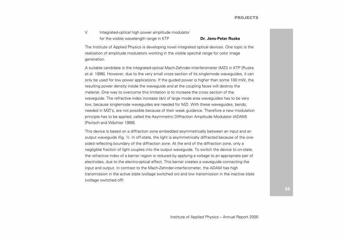
In order to measure the intensity distribution in the diffraction zone, a modulator chip was cut at
the end of the diffraction zone and this face was polished. By coupling light into the other end,
the changes of the optical field distribution within the diffraction zone can be measured by
means of a CCD-camera when a modulation voltage is applied (fig. 6).
-15 -10 -5 0 5 10 150
2
4
6
8
U / V
Fig.5 Output intensity of ADAM versus applied voltage.
PROJECTS
Institute of Applied Physics – Annual Report 2000
40
The performed measurements indicate that in contrast to MZI modulators the new type of
integrated electro-optical modulators has the potential to handle high optical powers in the
visible wavelength range. New applications in printing and display technology can be supported.
References
J.-P. Ruske, M. Rottschalk, B. Zeitner, V. Gröber, A. Rasch. Electr. Letters 34: 363 (1998)
T. Pertsch, C. Wächter. Optical and Quantum Electronics 31: 957 (1999)
M. G. Roelofs, P. A. Morris, J. D. Bierlein. J. Appl. Phys. 70: 720 (1991)
J. D. Bierlein and H. Vanderzeele. J.Opt. Soc. Am. B 6: 622 (1989) �
Fig.6 Intensity distribution at the end of the diffraction zone of ADAM at different voltages.

PROJECTS
Institute of Applied Physics – Annual Report 2000
41
VI. Microfabrication of optical waveguides
in transparent materials Dr. Stefan Nolte
At the Institute of Applied Physics, the investigation of the interaction between ultrashort laser
pulses and matter is one topic of research. Besides the study of the basic interaction process,
novel concepts for production technology based on laser machining are developed.
The fabrication of optical waveguides and waveguide arrays in different glasses and crystals is
required for many applications in integrated optics. At present, the waveguiding structures are
fabricated by ionic diffusion or exchange into a transparent substrate, by laser irradiation of
special photorefractive materials, or by lithographic methods. Although these technologies are
well established and successful, a quest for new, more flexible techniques allowing to fabricate
three-dimensional photonic structures continues.
Recently, a novel direct laser-writing technique, based on femtosecond laser pulses, has been
demonstrated. When tightly focused into the bulk of a transparent material, these pulses can
produce a permanent refractive index modification inside a small focal volume. In this volume,
the laser intensity is high enough for multiphoton absorption, optical breakdown, and
microplasma formation. The evolution of this microplasma, which is driven by free electrons,
induces structural (and refractive index) changes in the focal region by leaving a nonelastic
thermo-mechanical stress and/or by the formation of color centers. These mechanisms are
universal and allow to perform three-dimensional refractive index patterning and to fabricate
complicated photonic structures in practically every transparent material.
In the following, we report on investigations of the fabrication of waveguiding structures in
fused silica and crystalline quartz. For the microfabrication of the optical waveguides, 800 nm
laser pulses (Ti:Sapphire laser system) with a pulse duration of 120 fs and a pulse energy of a
few µJ are focused tightly into the bulk of the transparent sample by a microscope objective or
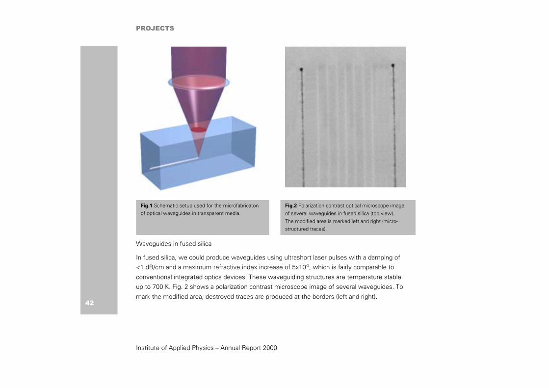
a lens with short focal length (see fig. 1). When the sample is moved with respect to the laser
beam axis, an optical waveguide can be produced, i.e. directly written into the material.
PROJECTS
Institute of Applied Physics – Annual Report 2000
42
Waveguides in fused silica
In fused silica, we could produce waveguides using ultrashort laser pulses with a damping of
<1 dB/cm and a maximum refractive index increase of 5x10⁻³, which is fairly comparable to
conventional integrated optics devices. These waveguiding structures are temperature stable
up to 700 K. Fig. 2 shows a polarization contrast microscope image of several waveguides. To
mark the modified area, destroyed traces are produced at the borders (left and right).
Fig.1 Schematic setup used for the microfabricatonof optical waveguides in transparent media.
Fig.2 Polarization contrast optical microscope image
of several waveguides in fused silica (top view).
The modified area is marked left and right (micro-structured traces).
PRO JECTS
Institute of Applied Physics – Annual Report 2000
43
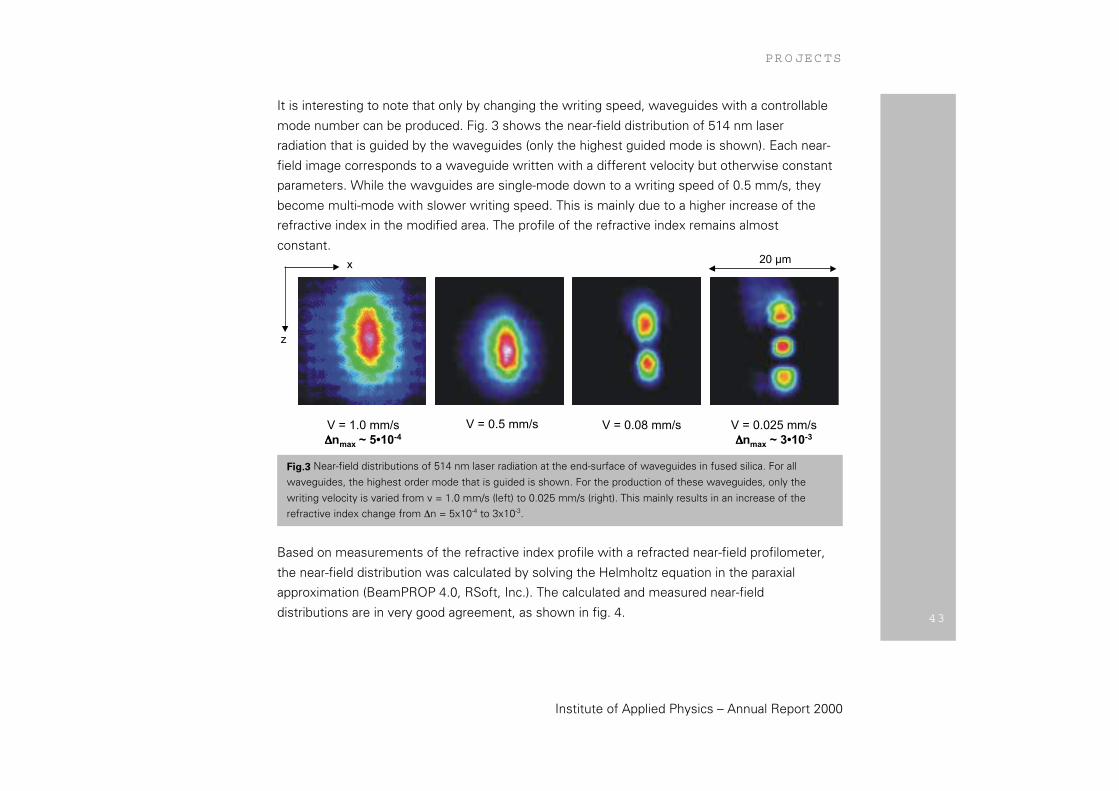
It is interesting to note that only by changing the writing speed, waveguides with a controllable
mode number can be produced. Fig. 3 shows the near-field distribution of 514 nm laser
radiation that is guided by the waveguides (only the highest guided mode is shown). Each near-
field image corresponds to a waveguide written with a different velocity but otherwise constant
parameters. While the wavguides are single-mode down to a writing speed of 0.5 mm/s, they
become multi-mode with slower writing speed. This is mainly due to a higher increase of the
refractive index in the modified area. The profile of the refractive index remains almost
constant.
Based on measurements of the refractive index profile with a refracted near-field profilometer,
the near-field distribution was calculated by solving the Helmholtz equation in the paraxial
approximation (BeamPROP 4.0, RSoft, Inc.). The calculated and measured near-field
distributions are in very good agreement, as shown in fig. 4.
20 µmx
z
V = 1.0 mm/snmax ~ 5•10-4
V = 0.5 mm/s V = 0.08 mm/s V = 0.025 mm/snmax ~ 3•10-3
Fig.3 Near-field distributions of 514 nm laser radiation at the end-surface of waveguides in fused silica. For all
waveguides, the highest order mode that is guided is shown. For the production of these waveguides, only the
writing velocity is varied from v = 1.0 mm/s (left) to 0.025 mm/s (right). This mainly results in an increase of therefractive index change from n = 5x10⁻⁴ to 3x10⁻³.

PRO JECTS
Institute of Applied Physics – Annual Report 2000
44
Waveguides in crystalline quartz
In crystalline materials, using ultrashort laser pulses can also produce waveguiding structures.
The observed refractive index increase of up to n 10-2, which is deduced from
interferometric analysis, is even higher than in glasses. These waveguide structures are stable
up to temperatures as high as 1500 K (for more than one hour).
Fig. 5 shows two polarization contrast optical microscope images of waveguides produced in
crystalline quartz. The left image shows a top view of several parallel waveguides written in
different depths, and in the right image, the magnified cross section (end view) of one of these
waveguides is displayed.
100 %
0 %
20 µm
(a)
20 µm
100 %
0 %
(b)
Fig.4 Comparison of the calculated (a) and measured (b) near-field distributionfor the highest order mode of the right waveguide of fig. 3.

PROJECTS
Institute of Applied Physics – Annual Report 2000
45
1 mm
y-cut(a)
(b)
Fig.5 Top view polarization contrast microscope image (left) of waveguides produced in crystalline quartz (spacing
between the waveguides is 0.5 mm). In the right image a cross section of one of the waveguides (polarization
contrast microscope) is shown.
(a)
20 µm
(b)
Fig.6 Near-field distributions of guided radiation at 514 nm. Different modes are guided.
PROJECTS
Institute of Applied Physics – Annual Report 2000
46
The image of the end view (fig. 5, right) shows details of the generated modifications inside the
material. The dark area corresponds to the laser beam focus; the bright areas correspond to the
induced stress. X-ray topography and transmission electron microscope (TEM) analysis of these
structures reveal that the crystalline structure in the central part is strongly disturbed. This core
is surrounded by an area with a deformed lattice, which is probably responsible for the
refractive index increase. Fig. 6 shows two different near-field distributions of 514 nm laser
radiation guided in these structures.
In conclusion
The use of ultrashort laser pulses allows producing waveguides in the bulk of transparent
materials. By carefully choosing the processing parameters, waveguides with different
properties can be designed in glasses as well as in crystalline materials. This could open up
new applications in integrated optics (e.g. the fabrication of 3-dimensional optical elements). �
PUBLICATIONS
Institute of Applied Physics – Annual Report 2000
47
Journals
I. U. Hinze, B. N. Chichkov, E. Tiemann, B. Wellegehausen: Resonant continuous four-
wave mixing and parametric amplification; J. Opt. Soc. Am. B., 17, 2001–10 (2000)
II. C. Reinhardt, B. N. Chichkov, B. Wellegehausen: Self-induced parametric amplification
of high-order harmonics; Opt. Lett. 25, 1043–5 (2000)
III. S. Meyer, B. N. Chichkov, B. Wellegehausen, A. Sanpera: Phase-matched high-order
harmonic generation and parametric amplification; Phys. Rev. A 61, 63811 (1–15) (2000)
IV. S. Meyer, B. N. Chichkov, B. Wellegehausen: High-order harmonic generation in
absorbing, disperse and ionizing media; Appl. Phys. B 70, pp. 221–25 (2000)
V. A. Tünnermann, H. Zellmer, W. Schöne, A. Giesen, K. Contag: New Concepts for
Diode Pumped Solid State Lasers; High-Power Diode Lasers, in: R. Diehl (Ed.): Topics
in Applied Physics Vol. 78, pp. 369–408, Springer Verlag, Heidelberg 2000
VI. J. Limpert, H. Zellmer, P. Riedel, A. Tünnermann: Laser Oscillation in the yellow and
green spectral range in Dy3+:ZBLAN; Electronics Letters 36, 16, pp. 1386–1387 (2000)
VII. D. M. Costantini, H. G. Limberger, T. Lasser, C. A. P. Muller, H. Zellmer, P. Riedel, A.
Tünnermann: Actively mode-locked visible up-conversion fiber laser; Optics Letters
25, 19, pp. 1445–1447 (2000)
VIII. A. Liem, D. Nickel, J. Limpert, H. Zellmer, U. Griebner, S. Unger, A. Tünnermann, G.
Korn: High avarage power ultrafast fiber CPA system; Applied Physics B, 71, 6, pp.
889–891 (2000)
IX. J. Limpert, H. Zellmer, A. Tünnermann, D. G. Lancaster, R. Weidner, D. Richter, F. K.
Tittel: Tunable continuous wave DFG-based gas sensor using fibre amplified 1.5 µm
external cavity diode laser and high power 1 µm diode laser; Electronics Letters 36,
1739 (2000)
PUBLICATIONS
Institute of Applied Physics – Annual Report 2000
48
X. E.-B. Kley, M. Cumme, L. Wittig, M. Thieme: Beam shaping elements for holographic
applications, micromachining and microfabrication; SPIE Vol. 4179, Santa Clara USA,
2000
XI. A. Schilling, P. Nußbaum, H. P. Herzig, E.-B. Kley: Fabrication technologies for
microoptical elements with arbitrary surfaces; SPIE Vol. 4179, Santa Clara USA, 2000
XII. T. Glaser, S. Schroeter, H.-J. Fuchs, E.-B. Kley: Experimental realization of a diffractive
optical isolator; SPIE Vol. 4179, Santa Clara USA, 2000
XIII. E.-B. Kley, M. Cumme, T. Clausnitzer, B. Schnabel, K. Zöllner, A. Stich: Investigation
of large area gratings fabricated by ultrafast e-beam writing; SPIE Vol. 4231, Chengdu,
China, 2000
XIV. B. Schnabel, E.-B. Kley: Evaluation and suppression of systematic errors in optical
subwavelength gratings; SPIE Vol. 4231, Chengdu, China, 2000
XV. E.-B. Kley, M. Cumme, L. Wittig, A. Tünnermann: Fabrication and properties of
refractive microoptical profiles for lenses, lens-arrays and beam shaping elements; SPIE
Vol. 4231, Chengdu, China, 2000
XVI. F. Korte, S. Adams, A. Egbert, C. Fallnich, A. Ostendorf, S. Nolte, M. Will, J.-P. Ruske,
B. N. Chichkov, A. Tünnermann: Sub-diffraction limited structuring of solid targets
with femtosecond laser pulses; Optics Express 7 (2), July 17, 2000, pp. 41–49
XVII. U. D. Zeitner, F. Wyrowski, H. Zellmer: External design freedom for optimization of
resonator originated beam shaping; IEEE J. Quantum Electron., 36 (10), 1105–1109
(2000)
XVIII. A. v. Pfeil, F. Wyrowski, A. Drauschke, H. Aagedal: Analysis of optical elements with
the local plane-interface approximation; Appl. Opt., 39(19), 3304–3313 (2000)

PUBLICATIONS
Institute of Applied Physics – Annual Report 2000
49
XIX. A. v. Pfeil, F. Wyrowski: Wave-optical structure design with the local plane-interface
approximation; J. Mod. Optics, 47(13), 2335–2350 (2000)
XX. H. Schimmel, F. Wyrowski: Amplitude matching strategy for wave-optical design of
monofuctional systems; J. Mod. Optics, 47, 2295–2321 (2000)
XXI. J. Turunen, M. Kuittinen, F. Wyrowski: Diffractive optics: electromagnetic approach; In
E. Wolf (editor): Progress in Optics; volume XL, chapter 5, pp. 343–388, North-Holland,
New York, 2000
XXII. D. Born, T. Wagner, W. Krech, U. Hübner, L. Fritzsch: Fabrication of Ultrasmall Tunnel
Junctions by Electron Beam Direct-Writing; IEEE Trans. Appl. Supercond. 2000
XXIII. K.-U.Barholz, M. Yu. Kupriyanov, U. Hübner, F. Schmidl, P. Seidel: An alternative
explanation of the „long-range proximity effect“ in HTS junctions; Physica C 334, 175-
184 (2000)
XXIV. Z. Bakonyi, G. Onishchukov, C. Knöll, M. Gölles, F. Lederer, R. Ludwig: 10 Gb/s RZ
transmission over 5000 km with gain-clamped semiconductor optical amplifiers and
saturable absorbers; Electronics Letters, v.35, N 21, pp. 1790–1791 (2000)
XXV. Z. Bakonyi, G. Onishchukov, C. Knöll, M. Gölles, F. Lederer, R. Ludwig: In-line
saturable absorber in cascaded SOA based transmission systems; IEEE Photonics
Technology Letters, v.12, N 5, pp. 570–572 (2000)
XXVI. M. Gölles, S. Darmanyan, F. Lederer, G. Onishchukov, A. Shipulin, Z. Bakonyi, V.
Lokhnygin: Modulational instability in a transmission system with semiconductor optical
amplifiers and in-line filters; Optics Letters, v.25, N 5, pp. 293–295 (2000)
XXVII. H. K. Tönshoff, C. Momma, A. Ostendorf, S. Nolte, G. Kamlage: Microdrilling of metals
with ultrashort laser pulses; J. Laser Appl. 12, 23 (2000)
PUBLICATIONS
Institute of Applied Physics – Annual Report 2000
50
XXVIII. S. Nolte, G. Kamlage, F. Korte, T. Bauer, T. Wagner, A. Ostendorf, C. Fallnich, H.
Welling: Micro-structuring with femtosecond lasers; Adv. Eng. Materials 2, 23 (2000)
Conference Contributions
I. A. Tünnermann, H. Zellmer: Hochleistungs-Faserlasersysteme im Sichtbaren und
Infraroten; L.O.B. 2000, Laser+Optik Berlin, March 8–9, 2000 (invited)
II. A. Tünnermann: Faserlaser und -verstärker – Neuartige Konzepte für kohärente
Strahlungsquellen im sichtbaren und nahinfraroten Spektralbereich; Atomphysikalisches
Kolloquium der Universität Bonn, 2000 (invited)
III. J. Limpert, H. Zellmer, P. Riedel, A. Tünnermann: Upconversion-Prozesse in
Dysprosium, Europium, Samarium und Terbium; Fachvortrag (invited), Frühjahrstagung
der DPG, Bonn, 2000
IV. A. Tünnermann, S. Nolte: Neue Trends in der Mikro- und Nanobearbeitung durch den
Einsatz von Ultrakurzpulslasern; Thüringer Lasersymposium, Jena, 2000 (invited)
V. S. Nolte, J.-P. Ruske, M. Will, A. Tünnermann: Mikrostrukturierung im Volumen
transparenter Materialien mit ultrakurzen Laserpulsen, Thüringer Lasersymposium,
Jena, 2000
VI. R. Schiek, W. Elflein, T. Pertsch, A. Tünnermann, K. R. Parameswaran, M. M. Fejer:
Femtosecond all-optical switching in a lithium niobate directional coupler with cascaded
nonlinearity; Nonlinear Optics: Materials, Fundamentals and Applications, Kaua‘i-Lihue,
Hawaii/USA, 2000 (invited)
VII. L. Wittig, E.-B. Kley, A. Tünnermann: Refraktive Strahlformer hergestellt durch
Elektronenstrahl- und Grautonlithographie; Mikrooptik-Workshop, Hagen, 2000 (invited)

PUBLICATIONS
Institute of Applied Physics – Annual Report 2000
51
VIII. M. Kempe, A. Kalies, D. Mühlhoff, G. Rudolph, P. Zöphel, A. Tünnermann, P. Riedel,
H. Zellmer: Upconversion Faserlaser für die Laserrastermikroskopie; 101.
Jahrestagung der DGAO 2000, June 13–16, 2000, Jena, Paper B29
IX. H. Zellmer, P. Riedel, A. Tünnermann, I. Freitag, P. Rottengatter: Noise Suppression
of a blue Upconversion Fiber Laser; CLEO Europe, September 10–15, 2000,
Nice/France, Paper CThE 43
X. H. Zellmer, A. Liem, P. Riedel, T. Gabler S. Unger: Fiber Amplifier Based High Power
Picosecond Source; CLEO Europe, September 10–15, 2000, Nice/France, Paper CWA
0002
XI. E.-B. Kley: Micro- and Nanomachining for Optics; International Conference Micro- and
Nano-Engineering 2000 (MNE 2000), September 18–21, 2000 (Plenary talk)
XII. L. Wittig, M. Cumme, T. Harzendorf, E.-B. Kley: Intermittence effect in electron
beam writing; Micro- and Nano-Engineering 2000, September 18–21, 2000 (Poster)
XIII. B. Schnabel, E.-B. Kley: On the influence of the e-beam writer address grid on the
optical quality of high-frequency gratings; Micro- and Nano-Engineering 2000,
September 18–21, 2000 (Poster)
XIV. M. Barge, S. Bruynooghe, F. Clube, A. Nobari, J.-L. Saussol, E. Grass, H. Mayer,
B. Schnabel, E.-B. Kley: 120 nm lithography at 364 nm wavelength using off-axis TIR
holography; Micro- and Nano-Engineering 2000
XV. U. Hübner, R. Plontke, M. Blume, A. Reinhardt, H. W. P. Koops: On-line
nanolithography using electron beam induced deposition technique; Micro- and Nano-
Engineering 2000, September 18–21, 2000
PUBLICATIONS
Institute of Applied Physics – Annual Report 2000
52
XVI. S. Wunderlich, F. Schmidl, L. Dörrer, C. Steigmeier, U. Hübner, P. Seidel: Planare
galvanisch gekoppelte dc-SQUID-Gradiometer auf 10x10 mm2 Bikristallen;
Frühjahrstagung der DPG, Regensburg, March 2000
XVII. M. Will, S. Nolte, J.-P. Ruske, T. Wagner, A. Tünnermann: Laserinduzierte
Brechzahlmodifikation in transparenten Medien zur Herstellung von integriert-optischen
Bauelementen; Fachvortrag (invited), Frühjahrstagung der DPG, Bonn, 2000
XVIII. E. A. Werner, J.-P. Ruske, B. Zeitner, W. Biehlig, A. Tünnermann: Integrated-optical
high power amplitude modulator for the visible wavelength range in KTP; CLEO2000,
Nice/France, CTHE27, p. 305
XIX. M. Will, S. Nolte, J.-P. Ruske, F. Wunderlich, A. Tünnermann: Laser written
waveguides in glasses and crystals; CLEO2000, September 10–15, 2000, Nice/France,
CMB6, p. 9
XX. C. Knöll, M. Gölles, F. Lederer, Z. Bakonyi, G. Onishchukov: Features of a saturable
absorber in a SOA signal transmission line; CLEO/Europe 2000, Nice/France, Technical
Digest, paper CTuD4, p. 62 (2000)
XXI. Z. Bakonyi, G. Onishchukov, C. Knöll, F. Lederer: Noise suppression by saturable
absorber in transmission systems with semiconductor optical amplifiers; CLEO2000,
San Francisco/USA, Technical Digest, paper CWK56, pp. 329–330 (2000)
XXII. A. Okhrimchuk, G. Onishchukov, F. Lederer: Long-haul soliton transmission in a
standard fiber at 1.3 µm with distributed Raman amplification; CLEO2000, San
Francisco/USA, Technical Digest, paper CWK71, pp. 343–344 (2000)
XXIII. Z. Bakonyi, C. Knöll, G. Onishchukov, F. Lederer: High bit rate fiber transmission
systems with saturable absorbers; IWKM 2000 14th International Scientific Conference
Mittweida, Mittweida, November 8–11, 2000

PUBLICATIONS
Institute of Applied Physics – Annual Report 2000
53
XXIV. G. Onishchukov, Z. Bakonyi, F. Lederer: 10 Gbit/s transmission in cascaded fiber
systems with gain-clamped semiconductor optical amplifiers and saturable absorbers;
DFG-Koloquium, Duisburg, July 3–4, 2000.
XXV. Z. Bakonyi, G. Onishchukov, C. Knöll, M. Gölles, F. Lederer: 10 Gb/s RZ transmission
in systems with combined absorber-semiconductor optical amplifier; COST 266/267,
Optical signal processing in Photonics Networks, Berlin, April 5–7, 2000 (Workshop)
XXVI. M. Will, T. Gorelik, S. Nolte, J.-P. Ruske, F. Wunderlich, A. Tünnermann: Properties
of waveguides manufactured with fs-laser pulses in transparent materials;
Norddeutscher Lasertag, Hannover, 2000
XXVII. S. Nolte, F. Korte, G. Kamlage, M. Will, B. Chichkov, A. Tünnermann:
Microstructuring of Solid Targets with Femtosecond Laser Pulses; RGLS,
Vladimir/Suzdal (Rußland), 2000
XXVIII. S. Nolte, F. Korte, G. Kamlage, M. Will, B. Chichkov, A. Tünnermann:
Microstructuring of Solid Targets with Femtosecond Laser Pulses; ULIA, Pisa/Italy,
2000
XXIX. F. Korte, T. Bauer, S. Nolte, A. Egbert, C. Fallnich, H. Welling: Microstructuring of
periodic patterns with femtosecond laser pulses; CLEO Europe 2000, Nice/France,
Technical Digest, p. 207, September 13, 2000 (Poster)
XXX. F. Korte, A. Egbert, S. Nolte, B. Chichkov, C. Fallnich, H. Welling: Nanostructuring
with femtosecond laser pulses; CLEO 2000, San Francisco/USA, Technical Digest, p.
374, May 15, 2000
XXXI. H. Tönshoff, A. Ostendorf, S. Nolte, G. Kamlage, T. Wagner, F. Korte, T. Bauer: New
applications of femtosecond lasers in micromachining; 1st euspen Topical Conference
on Fabrication and Metrology in Nanotechnology, Vol. 1, pp. 10–17,
Copenhagen/Denmark, May 28–30, 2000
PUBLICATIONS
Institute of Applied Physics – Annual Report 2000
54
XXXII. H. Tönshoff, A. Ostendorf, S. Nolte, F. Korte, T. Bauer: Micromachining using
femtosecond lasers; SPIE – Laser Precision Manufacturing 2000 Conference, pp.
136–139, Omiya/Japan, June 14–16, 2000
Patent Applications
I. J.-P. Ruske, H. Zellmer, A. Tünnermann: Direkt modulierbarer Laser; Patent Nr. 100
06 050, Applicant: LDT Gera
II. H. Zellmer, A. Tünnermann: Faseroptischer Verstärker; Patent Nr. 100 09 379,
Applicant: LDT Gera
III. Kränert, T. Gabler, H. Zellmer, A. Tünnermann: Faserverstärker; Patent Nr. 100 09
380, Applicant: LDT Gera
IV. Kränert, T. Gabler, H. Zellmer, A. Tünnermann: Anordnung zur Erzeugung roter,
grüner und blauer Laserstrahlung; Patent Nr. 100 09 381, Applicant: LDT Gera

ACTIVITIES
Institute of Applied Physics – Annual Report 2000
55
Fairs
MTT 2000 (Mikrotechnik Thüringen, Erfurt) Fiber laser, integrated-optical modulator
with scanner, beam-shaping elements
Optatech 2000 (Frankfurt/Main) Fiber laser, integrated-optical
modulator, beam-shaping elements
Convention
Annual Meeting of German Society of Applied Optics
(June 13–17, 2000, Jena)
Conference Chair: Prof. Dr. Frank Wyrowski
Organizing Activities
Prof. Dr. Andreas Tünnermann
CLEO/Europe 2000 (Nice/France) General Program Chair
CLEO2000 (Baltimore, Maryland/USA) Program Committee Member
„Solid state lasers“
MTT 2000 (Mikrotechnik Thüringen, Erfurt) Program Committee Counselor
BMBF-Leitprojekt (07/00) „MICROPHOT“ Network Coordinator
OptoNet e. V. Founder and member of the board
Forschungsschwerpunkt Optomatronik/
Zentrum für Optomatronik Member
Dr. Stefan Nolte
CLEO2001 (Baltimore, Maryland/USA) Program Committee Member
„Laser Applications and
Optical Instrumentation Systems“
ACTIVITIES
Institute of Applied Physics – Annual Report 2000
56
Dr. Holger Zellmer
CLEO/Europe 2000 (Nice/France) Program Committee Member
„Waveguide Lasers, Fiber Lasers
and Amplifiers“

CONTACT
Institute of Applied Physics – Annual Report 2000
57
Postal address Friedrich-Schiller-Universität Jena
Institut für Angewandte Physik
Max-Wien-Platz 1
D-07743 Jena
Germany
Location of the institute Beutenberg Campus
Winzerlaer Straße 10
D-07745 Jena
Phone/Fax +49 (0) 36 41. 65 76 –40/ –80
Internet http://iapnt.iap.uni-jena.de
Head of the institute: Prof. Dr. Andreas Tünnermann
Phone +49 (0) 3641. 6576 46 e-mail [email protected]
Optical design: Prof. Dr. Frank Wyrowski
Phone +49 (0) 3641. 6576 64 e-mail [email protected]
Microstructure technology: Dr. Ernst-Bernhard Kley
Phone +49 (0) 3641. 6576 47 e-mail [email protected]
Ultrafast optics: Dr. Stefan Nolte
Phone +49 (0) 3641. 6576 56 e-mail [email protected]
Optical communication systems: Dr. George Onishchukov
Phone +49 (0) 3641. 6576 60 e-mail [email protected]
Integrated optics: Dr. Jens-Peter Ruske
Phone +49 (0) 3641. 6576 45 e-mail [email protected]
Fiber and waveguide lasers: Dr. Holger Zellmer
Phone +49 (0) 3641. 6576 51 e-mail [email protected]

CONTACT
Institute of Applied Physics – Annual Report 2000
58