analysis of pcb variations for impedance control579110/fulltext01.pdf · 3 analysis of pcb...
TRANSCRIPT

Degree project inElectronics and Computer Systems
First level, 15.0 HECStockholm, Sweden
T I A N Y U A N W O
Analysis of PCB Variations forImpedance Control
K T H I n f o r m a t i o n a n d
C o m m u n i c a t i o n T e c h n o l o g y


1
Kungliga Tekniska Högskolan Skolan för informations- och kommunikationsteknik (ICT) Examinator: Bengt Molin, [email protected] Handledare: Mats Jonsson, [email protected] Författarnas e-postadress: [email protected] Utbildnngsprogram: Högskoleingenjörsutbilding i elektronik och datorteknik, 180hp Datum: 2012 Juni
Examensarbete inom elektronik- och datorsystem, grundnivå IL120X
ANALYSIS OF PCB VARIATIONS
FOR IMPEDANCE CONTROL
Tianyuan Wo

2
KTH Royal Institute of Technology School of Information and Communication Technology (ICT) Examiner: Bengt Molin, [email protected] Supervisor: Mats Jonsson, Ericsson, [email protected] Author: Tianyuan Wo, [email protected] Program: Degree program in electronics and computer Engineering, 180hp Date: 2012 June
Degree Project in Electronic- and Computer Systems, First Level, IL120X
ANALYSIS OF PCB VARIATIONS
FOR IMPEDANCE CONTROL
Tianyuan Wo

3
ANALYSIS OF PCB VARIATIONS
FOR IMPEDANCE CONTROL
Abstract Ericsson is a world-leading provider of telecommunications equipment and related services to mobile and fixed network operators globally. Over 1,000 networks in more than 175 countries utilize Ericsson’s network equipment and 40 percent of all mobile calls are made through their systems. Ericsson is one of the few companies worldwide that can offer end-to-end solutions for all major mobile communication standards. Tons of PCB is needed in this industry. With more complex hardware designs the need for efficient ways of controlling the impedance in our boards is increasing. Higher data rates and frequencies require better control of the PCB and understanding of the variations in the manufacturing of the PCB. The thesis goal is to study and research on how we can use cheaper PCB materials and handle the variations of these cheap PCB materials. This can be achieved with sorting out the spreading when it comes to conductor width & thickness, dielectric constant & thickness. One more area to explore is the variations of the dielectric constant due to glass cloth. How could statistical methods be used when looking at the variations of the material properties? Mathematica and Advanced Design System (ADS) were used to perform statistical analysis. The result of the thesis can help PCB designer to choose materials more wisely and provide advice to suppliers if they can achieve high quality products.

4

5
Contents
1 INTRODUCTION .............................................................................................................................................. 7
1.1 BACKGROUND ............................................................................................................................................. 7 1.2 THESIS PURPOSE .......................................................................................................................................... 7 1.3 LIMITATIONS OF THE TASK .......................................................................................................................... 8 1.4 METHOD ...................................................................................................................................................... 8
2 BACKGROUND THEORY ............................................................................................................................... 8
2.1 CHARACTERISTIC IMPEDANCE ..................................................................................................................... 8 2.2 MONTE CARLO SIMULATION ....................................................................................................................... 9 2.3 A SIMPLE EXAMPLE FOR HOW PCB VARIATIONS AFFECT THE CHARACTERISTIC IMPEDANCE ..................... 11
3 FACTORS THAT AFFECT THE DISTRIBUTION OF CHARACTERISTIC IMPEDANCE AND PASSING RATE ........................................................................................................................................................ 12
3.1 VARIABLES’ DISTRIBUTION ........................................................................................................................ 12 3.1.1 Mean, Standard deviation and Expectation ......................................................................................... 13 3.1.2 Distribution form .................................................................................................................................. 16
3.2 SENSITIVITY FOR VARIABLES ..................................................................................................................... 18 3.2.1 Introduction .......................................................................................................................................... 18 3.2.2 Relatively stable point .......................................................................................................................... 20 3.2.3 Variation estimation for outcomes ....................................................................................................... 21
3.3 PREPREG THICKNESS AFTER PRESSING ....................................................................................................... 25
4 REAL CASE STUDY ....................................................................................................................................... 27
4.1 GENERAL ANALYSIS .................................................................................................................................. 27 4.2 ANALYSIS BASED ON MULTEK AND GCE’S DATA ...................................................................................... 31
5 CONCLUSION ................................................................................................................................................. 32
6 REFERENCE LIST ......................................................................................................................................... 33
7 APPENDIX A – CHARACTERISTIC IMPEDANCE EXPRESSIONS ..................................................... 34
8 APPEDIX B – PARTIAL DERIVATIVES (DK=4.5) ................................................................................... 36
9 APPENDIX C- A SIMPLE ADS EXAMPLE FOR STATISTIC ANALYSIS ............................................ 39

Analysis of PCB Variations for impedance control Tianyuan Wo
6
Analysis of PCB Variations for impedance control Tianyuan Wo
7
1 INTRODUCTION
1.1 Background
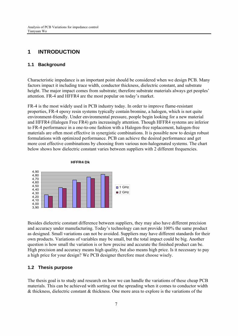
Characteristic impedance is an important point should be considered when we design PCB. Many factors impact it including trace width, conductor thickness, dielectric constant, and substrate height. The major impact comes from substrate; therefore substrate materials always get peoples’ attention. FR-4 and HFFR4 are the most popular on today’s market.
FR-4 is the most widely used in PCB industry today. In order to improve flame-resistant properties, FR-4 epoxy resin systems typically contain bromine, a halogen, which is not quite environment-friendly. Under environmental pressure, people begin looking for a new material and HFFR4 (Halogen Free FR4) gets increasingly attention. Though HFFR4 systems are inferior to FR-4 performance in a one-to-one fashion with a Halogen-free replacement, halogen-free materials are often most effective in synergistic combinations. It is possible now to design robust formulations with optimized performance. PCB can achieve the desired performance and get more cost effective combinations by choosing from various non-halogenated systems. The chart below shows how dielectric constant varies between suppliers with 2 different frequencies.
HFFR4 Dk
3,904,004,104,204,304,404,504,604,704,804,90
1 GHz
2 GHz
Besides dielectric constant difference between suppliers, they may also have different precision and accuracy under manufacturing. Today’s technology can not provide 100% the same product as designed. Small variations can not be avoided. Suppliers may have different standards for their own products. Variations of variables may be small, but the total impact could be big. Another question is how small the variation is or how precise and accurate the finished product can be. High precision and accuracy means high quality, but also means high price. Is it necessary to pay a high price for your design? We PCB designer therefore must choose wisely.
1.2 Thesis purpose
The thesis goal is to study and research on how we can handle the variations of these cheap PCB materials. This can be achieved with sorting out the spreading when it comes to conductor width & thickness, dielectric constant & thickness. One more area to explore is the variations of the

Analysis of PCB Variations for impedance control Tianyuan Wo
8
dielectric constant due to glass cloth. How could statistical methods be used when looking at the variations of the material properties? Mathematica and Advanced Design System (ADS) were used to perform statistical analysis.
1.3 Limitations of the task
The reliability of my study is all based on the reliability of the data from PCB suppliers. The quantity of their samples is not large enough to find out the real distribution of every variable. It should take hundreds or thousands of samples, but that large amount is not realistic. People assume usually all variables following normal distribution, and my study can only based on this assumption.
1.4 Method
I began my project with pilot study to understand the problem and find a proper way to solve it. Because I did not have any knowledge of PCB impedance, it took over a week. After that I tested Monte Carlo simulation on Advanced Design System, which is required by the customer.
My work consists of 4 parts: distribution study, sensitivity study, methodology creating, and report. Because my project is a research project, and report contains all results that should be delivered to the customer, I listed it in the main part of my work too. Every part took about 10 days, and I worked 8-9 hours a day.
My work place is near the supervisor’s office. We can easily contact with each other face to face, or via email. My question can be answered, and useful information can be delivered to me by an efficient way.
The tools used for the study are Advanced Design System and Mathematica. Advanced Design System has algorithms that run in black box to calculate characteristic impedance. Hardware designers in Ericsson use this tool to design circuits. The purpose of using this tool to simulate the outcomes is to create the possibility for future to use this tool to do simple distribution analysis by her/his self (a simple example in appendix c). The sensitivity analysis must be done by more professional math tools. In this project, I chose Mathematica to do the calculation and plotting.
2 BACKGROUND THEORY
2.1 Characteristic impedance Characteristic impedance is the ratio of the amplitudes of a single pair of voltage and current waves propagating along a uniform transmission line without reflections. It is usually written as

Analysis of PCB Variations for impedance control Tianyuan Wo
9
Z0 or Zc. Characteristic impedance is determined by 2 variables: the per-unit-length inductance L and the per-unit-length capacitance c of a line.1
When the loaded impedance is equal to the characteristic impedance, the wave will not be reflected. An existed circuit means that the value of Z0 has been determined; therefore we must be very careful when design and produce PCB. Any small changes could impact the result. In order to keep the reflection under an acceptable range, analysis of PCB variations is necessary.
The per-unit-length variables of PCB lands are very difficult to derive, and it will not be discussed in this thesis. However we can use some design tools, ADS for instance, to calculate the characteristic impedance. We can also find formulas in many literatures. Usually, these factors are given in terms of L and c: relative permittivity and thickness of the substrate, width and thickness of the trace, distance between traces. A table of characteristic impedance calculating for microstrip-line stands below. W is width of the strip, t is thickness of the strip, h is the thickness of the substrate and εr is the relative permittivity.
More tables can be found in Appendix A.
2.2 Monte Carlo Simulation Monte Carlo Simulation is a method that repeatedly takes random samples to compute the properties of some phenomenon or behavior. It is very useful when inputs have significant uncertainty. Monte Carlo simulation is widely used in science and engineering, including astrophysics, physical chemistry, biology, finance and many other areas. In electronics engineering, it is applied to analyze any correlated variations in circuits.
1 Clayton R.Paul, (2010), Transmission Lines in Digital and Analog Electronic Systems: Signal Integrity and Crosstalk. Wiley, ISBN 978-0-470-59230-4

Analysis of PCB Variations for impedance control Tianyuan Wo
10
Monte Carlo Simulation works this way: Get random value for each variable Compute the outcome Repeat step 1 and step 2 as many times as possible to produce hundreds or thousands of
possible outcomes. Analyze the results to get probabilities of different outcomes occurring.
The “random value” is not always required to be truly random. It is more useful to generate pseudorandom sequences that appear random enough and approximate the properties of these variables. That means that the known distributions of variables should pass statistical tests and be proved. Shlomo Sawilowsky lists the requirements for a high quality Monte Carlo Simulations:2
The (pseudo-random) number generator has certain characteristics (e.g., a long “period” before the sequence repeats)
The (pseudo-random) number generator produces values that pass tests for randomness There are enough samples to ensure precise results The proper sampling technique is used The algorithm used is valid for what is being modeled It simulates the phenomenon in question.
In my study, Process Capability Index Values, which indicates how much “natural variation” a process experiences relative to its specification, are available form PCB suppliers, and is considered reliable. All results depend on the data from suppliers. The main advantage of Monte Carlo Simulation is simplicity. Specific knowledge of the solution is not required. It is also easy to implement on a computer. The main disadvantage is slowness. In order to get precise result, thousands or even millions samples may be needed, and surely that will take time.
2 Sawilowsky, Shlomo S.; Fahoome, Gail C. (2003). Statistics via Monte Carlo Simulation with FORTRAN. Rochester Hills, MI: JMASM. ISBN 0-9740236-0-4)
Analysis of PCB Variations for impedance control Tianyuan Wo
11
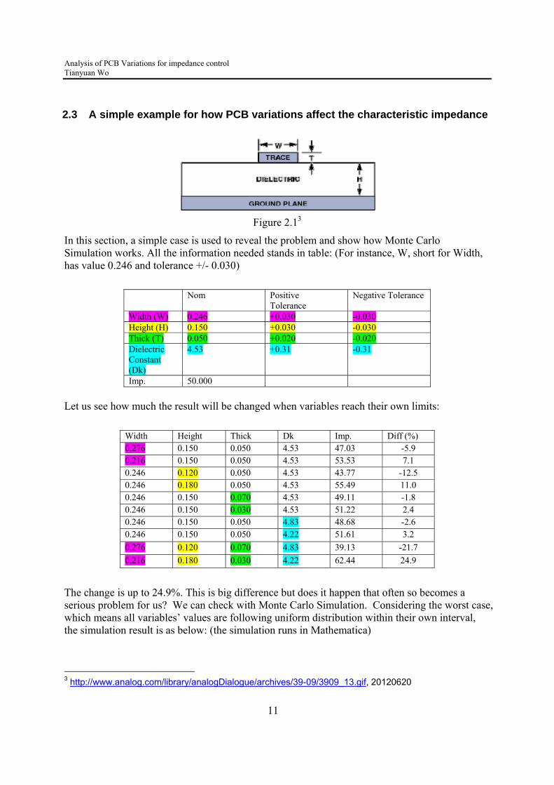
2.3 A simple example for how PCB variations affect the characteristic impedance
Figure 2.13
In this section, a simple case is used to reveal the problem and show how Monte Carlo Simulation works. All the information needed stands in table: (For instance, W, short for Width, has value 0.246 and tolerance +/- 0.030)
Nom Positive Tolerance
Negative Tolerance
Width (W) 0.246 +0.030 -0.030 Height (H) 0.150 +0.030 -0.030 Thick (T) 0.050 +0.020 -0.020 Dielectric Constant (Dk)
4.53 +0.31 -0.31
Imp. 50.000
Let us see how much the result will be changed when variables reach their own limits:
Width Height Thick Dk Imp. Diff (%) 0.276 0.150 0.050 4.53 47.03 -5.9 0.216 0.150 0.050 4.53 53.53 7.1 0.246 0.120 0.050 4.53 43.77 -12.5 0.246 0.180 0.050 4.53 55.49 11.0 0.246 0.150 0.070 4.53 49.11 -1.8 0.246 0.150 0.030 4.53 51.22 2.4 0.246 0.150 0.050 4.83 48.68 -2.6 0.246 0.150 0.050 4.22 51.61 3.2
0.276 0.120 0.070 4.83 39.13 -21.7
0.216 0.180 0.030 4.22 62.44 24.9
The change is up to 24.9%. This is big difference but does it happen that often so becomes a serious problem for us? We can check with Monte Carlo Simulation. Considering the worst case, which means all variables’ values are following uniform distribution within their own interval, the simulation result is as below: (the simulation runs in Mathematica)
3 http://www.analog.com/library/analogDialogue/archives/39-09/3909_13.gif, 20120620

Analysis of PCB Variations for impedance control Tianyuan Wo
12
Figure 2.2
From the histogram of PDF, we see that the possibility that characteristic impedance has value 62.44 is very small. Most results are between 45 and 55 ohm. With help of Monte Carlo simulation, the distribution of characteristic impedance can be estimated, and further more we can estimate the passing rate of product from every supplier. In this example, characteristic impedance is normally distributed. This can be verified by probability plot:
Figure 2.3
If the tolerance of characteristic impedance is +/- 8 ohm, the passing rate would be ca 95%.
3 FACTORS THAT AFFECT THE DISTRIBUTION OF CHARACTERISTIC IMPEDANCE AND PASSING RATE
3.1 Variables’ distribution The most apparent factor must be variables’ distribution. If income values were as we expected, all problems would not exist. We can also simply notice the difference when a variable changes from a highly concentrated distribution to uniform distribution. This may seem simple, but we actually can dig little deeper.

Analysis of PCB Variations for impedance control Tianyuan Wo
13
3.1.1 Mean, Standard deviation and Expectation
Suppose we have sample space . Then mean is defined via the equation4
.
For instance, we collected a set of trace width: 0.246mm, 0.242mm, 0.250mm, 0.257mm, 0.245mm, then the mean of this set was 0.248mm. Every single element in this set can be approved according to the requirement 0.246 ± 0.030 mm, but the mean does not have to be the same as the expected value 0.246. The difference does cause difference between characteristic impedances’ mean and its expected value, and this may lead to lower passing rate. The example in Chapter 2 is used as reference here to show the difference:
The only thing changed here is the mean of trace width. Run again Monte Carlo Simulation we see the change.
Figure 3.1
If the tolerance of characteristic impedance was ± 5 ohm, the passing rate would decrease from 81% to 79%.
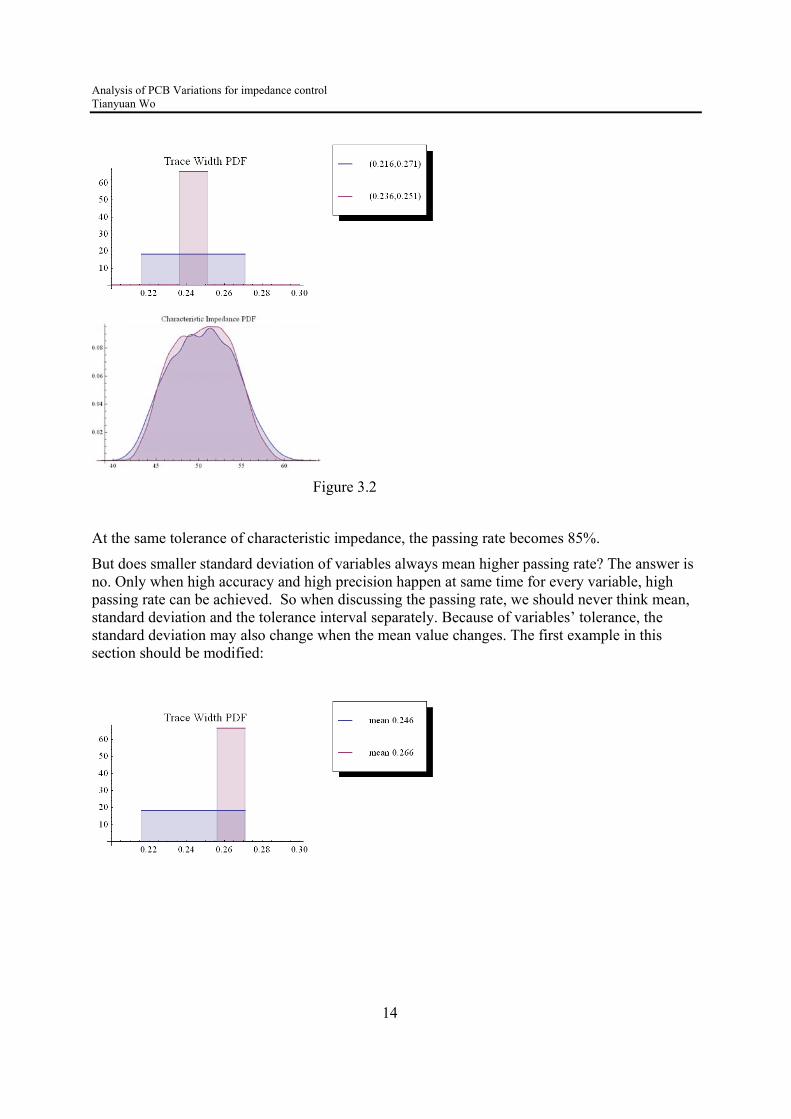
Standard deviation is another factor that will be discussed here. Small value of standard deviation means small variation and high precision. This affects also result. (Figure 3.2)
4Mean : http://en.wikipedia.org/wiki/Arithmetic_mean, 20120620
Analysis of PCB Variations for impedance control Tianyuan Wo
14
Figure 3.2
At the same tolerance of characteristic impedance, the passing rate becomes 85%.
But does smaller standard deviation of variables always mean higher passing rate? The answer is no. Only when high accuracy and high precision happen at same time for every variable, high passing rate can be achieved. So when discussing the passing rate, we should never think mean, standard deviation and the tolerance interval separately. Because of variables’ tolerance, the standard deviation may also change when the mean value changes. The first example in this section should be modified:

Analysis of PCB Variations for impedance control Tianyuan Wo
15
Figure 3.3
The passing rate is now 80.5%. It is almost the same as the reference group with 0.246 as the mean. In more extreme case, the passing rate of result with highly concentrated incomes could be lower than the passing rate of these with uniformly distributed incomes. In this particular case, the passing rate would stop here, if we did not change the mean of trace width and any value of other variables, no matter how hard we were trying to narrow down the variation of trace width.
Figure 3.4
Let us see a more complex case (figure 3.4). The blue area is still for the reference set. The red and yellow areas are for two sets of outcomes with different means but same variation. The simulation result is in table below:

Analysis of PCB Variations for impedance control Tianyuan Wo
16
Group Mean Standard Deviation
(50+/- 5 ohm) Passing Rate
Blue (ref.) 50.3 3.82 81%
Red 47.6 3.31 77.4%
Yellow 53.0 3.57 69.7%
This table shows that the mean of variable affects also result’s variation. How does this happen? The diagram below may help us understand.
20 40 60 80 100change of parameters ���
�100
�50
50
100
change of Z0 ���
Thickness
Thickness
Height�
Height�
Dk�
Dk�
Width�
Width�
Figure 3.5
This diagram shows how many percents the result changes when every single variable increases or decreases from a particular point, there width = 0.246, Dk =4.53, Height= 0.150 and Thickness=0.050. We see the characteristic impedance changes much more quickly when trace width decreases than when it increases. With same size of variation, the set of trace width that has larger average value, gives larger variation of result. That is the real reason why mean of variable can affect the variation of the result.
3.1.2 Distribution form We notice that we can get smaller standard deviation of characteristic impedance by adjusting the distribution form of every variable, not simply just their standard deviation or mean. Different distributions may give same results, or oppositely, similar distributions give totally different results. We can imagine how big improvement could be when we use normal distribution in stead of uniform distribution, but considering the fact shown in figure 3.5, a skew normal distribution may give even better result. Therefore the data that how every single variable is distributed is important for PCB variations analysis.

Analysis of PCB Variations for impedance control Tianyuan Wo
17
But in reality, it could be hard to gather enough data to find out the actual distribution of every variable. We usually assume they follow normal distribution. Process capability index5 and other values provided by supplier are all based on this assumption. The commonly-accepted process capability index includes Cp, Cp, lower, Cp, upper, Cpk and so on. Suppliers provide Cpk value to indicate process yield of every single variable. As long as Cpk value is larger than 1, we can say the process yield is 100%. How close Cpk is to Cp tells us how far the mean of the set is from the center of the interval. If Cpk appears alone without Cp or mean, it is meaningless for PCB variations analysis. Suppliers usually provide only Cp and Cpk. In fact, the distribution shifted up or down is also important. Figure 3.7 shows what happens
Figure 3.7
Results: Group Mean Standard
Deviation (50+/- 5 ohm) Passing Rate
0.99 Confidence Level
Blue (ref.) 50.2 3.51 84.5% (41.2, 59.3)
Red (up) 49.1 3.45 84.4% (40.4, 58.0)
Yellow (down) 51.3 3.55 80.8% (42.1, 60.6)
The passing rate is barely changed when we compare blue and red areas, but yellow area gives a lower passing rate. We can also see the difference of their 0.99 confidence intervals. The red set has the smallest size while the yellow set has the largest.
5Process capability index: http://en.wikipedia.org/wiki/Process_capability_index, 20120620
Analysis of PCB Variations for impedance control Tianyuan Wo
18
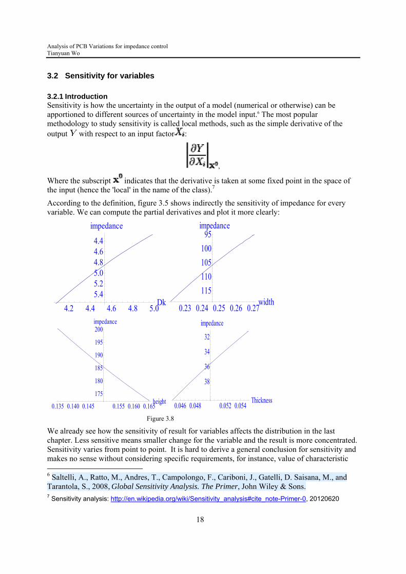
3.2 Sensitivity for variables
3.2.1 Introduction Sensitivity is how the uncertainty in the output of a model (numerical or otherwise) can be apportioned to different sources of uncertainty in the model input.6 The most popular methodology to study sensitivity is called local methods, such as the simple derivative of the output with respect to an input factor :
,
Where the subscript indicates that the derivative is taken at some fixed point in the space of the input (hence the 'local' in the name of the class).7
According to the definition, figure 3.5 shows indirectly the sensitivity of impedance for every variable. We can compute the partial derivatives and plot it more clearly:
4.2 4.4 4.6 4.8 5.0Dk
�5.4�5.2�5.0�4.8�4.6�4.4
�impedance
0.23 0.24 0.25 0.26 0.27width
�115
�110
�105
�100
�95�impedance
0.135 0.140 0.145 0.155 0.160 0.165height
175
180
185
190
195
200�impedance
0.046 0.048 0.052 0.054Thickness
�38
�36
�34
�32
�impedance
Figure 3.8
We already see how the sensitivity of result for variables affects the distribution in the last chapter. Less sensitive means smaller change for the variable and the result is more concentrated. Sensitivity varies from point to point. It is hard to derive a general conclusion for sensitivity and makes no sense without considering specific requirements, for instance, value of characteristic 6 Saltelli, A., Ratto, M., Andres, T., Campolongo, F., Cariboni, J., Gatelli, D. Saisana, M., and Tarantola, S., 2008, Global Sensitivity Analysis. The Primer, John Wiley & Sons. 7 Sensitivity analysis: http://en.wikipedia.org/wiki/Sensitivity_analysis#cite_note-Primer-0, 20120620
Analysis of PCB Variations for impedance control Tianyuan Wo
19
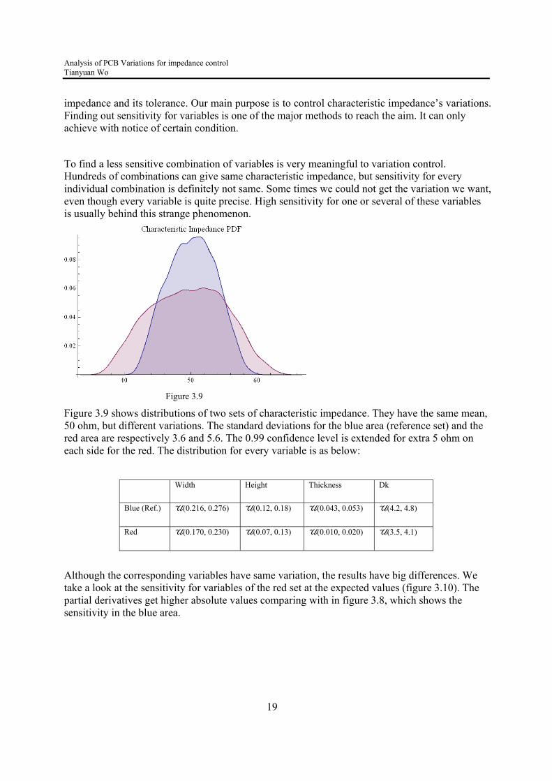
impedance and its tolerance. Our main purpose is to control characteristic impedance’s variations. Finding out sensitivity for variables is one of the major methods to reach the aim. It can only achieve with notice of certain condition.
To find a less sensitive combination of variables is very meaningful to variation control. Hundreds of combinations can give same characteristic impedance, but sensitivity for every individual combination is definitely not same. Some times we could not get the variation we want, even though every variable is quite precise. High sensitivity for one or several of these variables is usually behind this strange phenomenon.
Figure 3.9
Figure 3.9 shows distributions of two sets of characteristic impedance. They have the same mean, 50 ohm, but different variations. The standard deviations for the blue area (reference set) and the red area are respectively 3.6 and 5.6. The 0.99 confidence level is extended for extra 5 ohm on each side for the red. The distribution for every variable is as below:
Width Height Thickness Dk
Blue (Ref.) U(0.216, 0.276) U(0.12, 0.18) U(0.043, 0.053) U(4.2, 4.8)
Red U(0.170, 0.230) U(0.07, 0.13) U(0.010, 0.020) U(3.5, 4.1)
Although the corresponding variables have same variation, the results have big differences. We take a look at the sensitivity for variables of the red set at the expected values (figure 3.10). The partial derivatives get higher absolute values comparing with in figure 3.8, which shows the sensitivity in the blue area.

Analysis of PCB Variations for impedance control Tianyuan Wo
20
3.5 3.6 3.7 3.9 4.0 4.1Dk
�6.6�6.4�6.2�6.0
�5.6�5.4�5.2
�impedance
0.18 0.19 0.21 0.22width
�160�155�150�145
�135�130�125�impedance
0.090 0.095 0.105 0.110height
280
290
310
320�impedance
0.01650.01700.0175 0.01850.01900.0195Thickness
�92
�90
�88
�86
�84
�82
�impedance
Figure 3.10
3.2.2 Relatively stable point Impedance is given by many signals, and usually has been decided before designing the layout. For Microstrip line, we can get the most stable combination which gives particular value of characteristic impedance by setting values of dielectric constant, trace width and conductor thickness as large as possible and then adapting the dielectric substrate height to the result. For strip line, we in stead adapt the trace width to the particular value. For coupled lines, distance between lines usually has small impact on characteristic impedance, but sensitivities for other variables increase slightly with the distance’s growing. The major impact still comes from trace width. This is all under ideal condition. In reality we have no many choices for these variables. Conductor thickness is usually 17 um for inner layer and 50 um for outer layer. Dielectric thickness is 0.15 mm for 14-20 layers PCB and ≥ 0.20 mm for ≤ 14 layers. This means trace width for single ended line has been also decided. For coupled lines, the most stable point is determined by both space distance and trace width. The table below gives the relatively stable combinations for coupled strip lines:

Analysis of PCB Variations for impedance control Tianyuan Wo
21
Assuming characteristic impedance has not been decided, we can find the comparatively most stable point by setting trace as wide as possible. The narrower the trace is, the more sensitive the characteristic impedance is for it. All of the partial derivatives become smaller with growing of trace width.
3.2.3 Variation estimation for outcomes Another thing sensitivity can help us is to find the critical variables. “Critical” here means affecting the variation of result most. In order to get the variation we can accept, comparatively stricter requirement may be set for them. We can easily change the result’s variation by changing the critical variables’ variations. On the other side, if the critical variables have too large variation,
Diff. impedance
Dielectric constant
Dielectric thickness 0.15mm Dielectric thickness 0.20mm
Trace width(mm)
Space distance(mm)
Trace width(mm)
Space distance(mm)
100 ohm diff
4.1 0.10 0.20 0.14 0.25
4.2 0.10 0.22 0.14 0.28
4.3 0.10 0.25 0.13 0.24
4.4 0.10 0.29 0.13 0.26
4.5 0.09 0.21 0.13 0.29
4.6 0.09 0.25 0.12 0.25
4.7 0.09 0.27 0.12 0.27
4.8 0.09 0.3 0.12 0.3
50 ohm diff 4.1 0.37 0.26 0.5 0.27
4.2 0.37 0.41 0.5 0.32
4.3 0.36 0.29 0.5 0.45
4.4 0.36 0.43 0.49 0.45
4.5 0.35 0.32 0.48 0.40
4.6 0.34 0.25 0.47 0.37
4.7 0.34 0.31 0.47 0.50
4.8 0.33 0.26 0.46 0.44

Analysis of PCB Variations for impedance control Tianyuan Wo
22
the result’s variation can hardly be changed, no matter how hard we try to narrow other variables’ interval.
Figure 3.10
Figure 3.11 shows the effect after tolerance interval of a variable has been reduced. Both height and width was reduced by same size in millimeter. The sensitivities for them are respectively 255 and 145.
With notice of the limits for conductor thickness and dielectric height, we can find out the critical variables. For microstrip lines, dielectric substrate height is always one of the most important, the derivative for height is always over 100, even when the trace width is 1 mm; trace width can also be a very sensitive variable when its value is lower than 0.15mm (derivative’s absolute value is over 150 ). When trace is wider than 0.4 mm, its derivative can be around -50. Comparing with microstrip, strip lines are more stable under the same condition. Dielectric substrate height is no longer an extremely sensitive variable. Its derivative is between 50 and 100. Trace width influences now conductor thickness quite much. The derivative’s absolute value for thickness is over 100 when traces width smaller than 0.3mm; the derivative’s absolute values for both thickness and width are over 100 when traces width smaller than 0.16 mm; the derivative’s absolute values for thickness and width are over respectively 200 and 150 when traces width smaller than 0.1 mm.
How strict requirements for these critical variables should be depends on how precise and accurate we want the result to be, or the precision and the accuracy the product can reach. It can not be determined here. But at least we know conductor thickness and dielectric constant need not much attention.
When variables’ variations are small, we can estimate the size of result’s possible deviation as below:
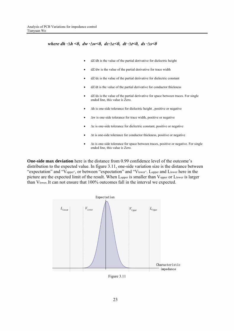
Upper-Side max deviation
|(dZ/dh) ·∆h+(dZ/ dw) ·∆w+ (dZ/dε)·∆ε+(dZ/ dt) ·∆t+(dZ/ds) ·∆s| (3.1.1)
where dh ·∆h >0, dw ·∆w>0, dε·∆ε>0, dt ·∆t>0, ds ·∆s>0
Lower-Side max deviation
|(dZ/dh) ·∆h +(dZ/ dw) ·∆w+ (dZ/dε)·∆ε+(dZ/ dt) ·∆t+ (dZ/ds) ·∆s | (3.1.2)
Analysis of PCB Variations for impedance control Tianyuan Wo
23
where dh ·∆h <0, dw ·∆w<0, dε·∆ε<0, dt ·∆t<0, ds ·∆s<0
dZ/dh is the value of the partial derivative for dielectric height
dZ/dw is the value of the partial derivative for trace width
dZ/dε is the value of the partial derivative for dielectric constant
dZ/dt is the value of the partial derivative for conductor thickness
dZ/ds is the value of the partial derivative for space between traces. For single ended line, this value is Zero.
∆h is one-side tolerance for dielectric height , positive or negative
∆w is one-side tolerance for trace width, positive or negative
∆ε is one-side tolerance for dielectric constant, positive or negative
∆t is one-side tolerance for conductor thickness, positive or negative
∆s is one-side tolerance for space between traces, positive or negative. For single ended line, this value is Zero.
One-side max deviation here is the distance from 0.99 confidence level of the outcome’s distribution to the expected value. In figure 3.11, one-side variation size is the distance between “expectation” and “Vupper”, or between “expectation” and “Vlower”. Lupper and Llower here in the picture are the expected limit of the result. When Lupper is smaller than Vupper or Llower is larger than Vlower, It can not ensure that 100% outcomes fall in the interval we expected.
Figure 3.11

Analysis of PCB Variations for impedance control Tianyuan Wo
24
Take the case in Chapter 2.3 for example.
dz/dh=185, dz/dw= -105, dz/dε= -4.82, dz/dt= -40, dz/ds=0, ∆h=±0.03, ∆w=±0.03, ∆ε=±0.31, ∆t=±0.02, ∆s=0
Upper-Side variation size= Lower-Side variation size
= |dz/dh| ·|∆h|+ |dz/dw| ·|∆w|+ |dz/dε|·|∆ε|+ |dz/dt| ·|∆t|+ |dz/ds| ·|∆s|
=5.55+3.15+1.55+0.8+0
=11.05
The estimated limits: 49.99+11.05=61.04; 49.99-11.05= 38.94
Comparing with the real limits 39.13 and 62.44, the estimation is pretty close to the simulation result.
However, the main purpose of using this equation is not to compute the minimal and maximal possible values of the outcomes. It can be done by setting every variable to its limit as I have done in chapter 2. What the equation can help us is to roughly get the tolerance for those critical variables that give a certain impedance interval. For instance, now we want the max deviation of the outcomes in chapter 2.3 to be 5, the equation can be created:
5-(|(dz/dε)·∆ε+ (dz/dt) ·∆t|) = |(dz/dh)·∆h+ (dz/dw)·∆w| =>
2.65 = -105∆w +185∆h, where ∆w<0, ∆h >0
Or, -2.65 = -105∆w +185∆h, where ∆w>0, ∆h <0
∆w and ∆h can be calculated according to other conditions, such as “∆h must be greater than 0.01mm”. Of course we can use mathematic tools to compute ∆w and ∆h. It is certainly that the result would be much more correct by using professional tools, but it needs also skills. My method is easier to apply.
When variable’s deviation is smaller than the distance from the limit to the expected value, we can be satisfied with all the outcomes. But we always want more outcomes to be close to the expected value .In order to achieve high accuracy in result, mean of critical variable discussed in the last section should be also considered. Sensitivity reveals not only how far every single event is shifted from the expectation, but also the tendency when most variables change their value towards a particular point. We see in earlier examples that the result is always more concentrated around the value that the variables’ means give. Therefore the result’s mean will also change, when a variable’s mean change. For those critical variables, the result’s mean changes more. It is actually quite important to set requirement for critical variables’ mean, but I did not see any in the documents I could access. According to my experience of studies, the following equation for can get pretty good result:
0
0,,
exp,0
Pa
Zn
Vuppermeana
D ectedupperZ
(3.2.1)

Analysis of PCB Variations for impedance control Tianyuan Wo
25
0
0,,
,0exp
Pa
Zn
Vlowermeana
D lowerZected
(3.2.2)
Z0: characteristic impedance
P0: a particular point there all variables of Z0 are decided
a: one variable of Z0
n: the total number of critical variables
V expected: The expected value of outcome
µZ0, upper: the wished upper limit of outcomes’ mean
µZ0, lower: the wished lower limit of outcomes’ mean
D a, mean, upper: estimated upper side max deviation of the variable’s mean
D a, mean, lower: estimated lower side max deviation of the variable’s mean
3.3 Prepreg thickness after pressing Laminate consists of glass fiber and epoxy. Dielectric constant of laminate can be expressed as such:
epoxyglass
epoxyepoxyglassglassatela HH
HDkHDkk
minD (3.3)
Correlation of dielectric constant and dielectric substrate’s height can also affect characteristic impedance.
Prepreg flows slightly during lamination process and fills the gap between traces. By this way copper traces are embedded in the prepreg and the thickness of prepreg is changed. The equation for prepreg thickness after pressing is as below:8
areacopper removed
cknesscopper thi areacopper remaining thicknessfinished
prepreg of thicknessFinal
This leads to different height for dielectric substrate. The extra height comes all from epoxy. If we know laminate has dielectric constant Dk0 when height is H0, the dielectric constant can be computed when height is changed slightly by H:
8 Istvan Nagy, How to calculate PCB trace width and differential pair separation, based on the impedance requirement and other variables
Analysis of PCB Variations for impedance control Tianyuan Wo
26
))((
)()()(
)(
)(
0
0000
0
00
00
0
00
0
0
HHDkDk
DkDkHDkDkDkHDkDkDkHDk
HH
HHDkHDkDk
HDkDk
DkDkH
HDkDk
DkDkH
H
HDkHHDkDk
HH
HDkHDkDk
HHH
glassepoxy
glassepoxyepoxyglassepoxyepoxyglass
epoxyepoxyglassglass
glassepoxy
epoxyglass
glassepoxy
glassepoxy
epoxyepoxyepoxyglass
epoxyglass
epoxyepoxyglassglass
epoxyglass
Dielectric constant is 6 for glass and 3 for epoxy. If set the value in the equation, we can get:
HH
HDk
HH
HDkDkDk
0
00
0
00
)3(3
)3( (3.4)
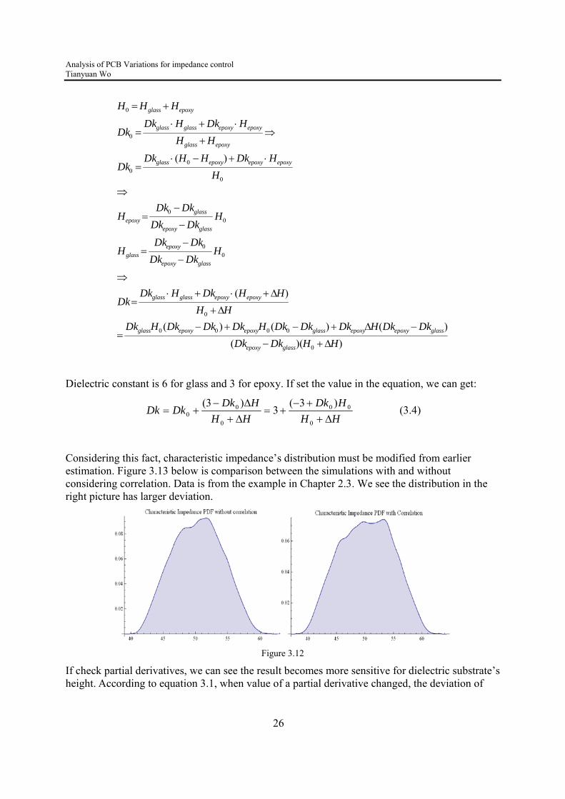
Considering this fact, characteristic impedance’s distribution must be modified from earlier estimation. Figure 3.13 below is comparison between the simulations with and without considering correlation. Data is from the example in Chapter 2.3. We see the distribution in the right picture has larger deviation.
Figure 3.12
If check partial derivatives, we can see the result becomes more sensitive for dielectric substrate’s height. According to equation 3.1, when value of a partial derivative changed, the deviation of

Analysis of PCB Variations for impedance control Tianyuan Wo
27
result changed at the same time. Now the derivative for height is increased, the final derivation should also be increased. It meets the simulation result.
Correlation of dk and height has no effect on other variables in single ended line. Their derivatives are exactly same with or without correlation. For coupled lines, effect on other variables is extremely small. The influence on height is more obvious in microstrip. The difference between the derivatives with and without correlation can be over 100 when the trace is very narrow, but it can be reduced with increasing of trace width. For strip line, the influence can be ignored when trace is wider than 0.25 mm.
Check appendix B partial derivatives if interested in the difference.
4 REAL CASE STUDY
4.1 General Analysis
Because of lack of data, it is almost impossible to compute the real distribution of characteristic impedance for every supplier. In order to reveal the result could happen according to the specification, this general analysis is necessary.
As discussed before, the mean value of every variable can affect the result, even if all test values are in the interval as the specification defined. Passing rate could change dramatically, especially when standard deviation of this variable is small. In this analysis, the mean values of variables are assumed to meet the expectation. The correlation between dielectric constant and dielectric thickness is considered.
Specification
Distribution of variables
Under real manufacturing, it is unlikely for every single variable to follow uniform distribution, which is worst case for both supplier and Ericsson. Most possible situation is that they follow normal distribution or some distribution form close to normal distribution. Uniform distribution may show the worst case we get, but also meaningless when the worst case is too far away from
Variable Line Width
Dielectric thickness inner layer
Dielectric thickness outer layer
Copper thickness inner layer
Copper thickness outer layer
Requirement 100 ±30 um
200±30 um (core) 200±38 um (prepreg)
60 ± 20 um
17 +3/-7 um
40 +20/-15 um

Analysis of PCB Variations for impedance control Tianyuan Wo
28
the expectation and has very low possibility to happen. Normal distribution is used here to show the most common result. For copper thickness, Skew normal distribution is used.
Define Standard deviation and Mean
Mean is simply set to the expected value.
Standard deviation should let nearly all the samples fall in the tolerance interval. So I set
Standard deviation = (Upper limit- Lower limit)/6
Variable Line Width Dielectric thickness inner layer
Dielectric thickness outer layer
Copper thickness inner layer
Copper thickness outer layer
Distribution N(100,10) N(200,10) (core) N(200,12.7) (prepreg)
N(60,6.7) Skew Normal Distribution [19,2.6,-10]
Skew Normal Distribution [34.6,7.3,2.8]
Simulation plotting
1) Microstrip line
40 50 600
0.20
0.40
0.60
0.80
1.00
PDF CDF
4.0 4.2 4.4 4.6 4.8 5.0Dk0
�5.2
�5.0
�4.8
�4.4
�4.2
�impedance
0.08 0.09 0.11 0.12width
�320
�300
�280
�260
�240
�220
�impedance

Analysis of PCB Variations for impedance control Tianyuan Wo
29
0.050 0.055 0.065 0.070height
480
500
520
560
580
600
620
�impedance
,
0.036 0.038 0.042 0.044Thickness
�20
�15
�10
�5
�impedance
SENSITIVITY
Normality fit test: 0.938306. Characteristic impedance is normal distributed. Mean value: 48.6915 Standard deviation: 4.35672 (worst case 7.7) Min value: 31 Max value: 69 95% confidence interval (33.6, 66.8), which means 95% of simulation results are between 40.15 ohm and 57.23 ohm.
2) Strip line
50 55 60 65 70 75
0.20
0.40
0.60
0.80
1.00
PDF CDF
4.0 4.2 4.4 4.6 4.8 5.0Dk0
�8.0
�7.5
�7.0
�6.5
�6.0
�impedance
0.08 0.09 0.11 0.12width
�280
�260
�220
�200�impedance
Analysis of PCB Variations for impedance control Tianyuan Wo
30
0.16 0.18 0.22 0.24height
90
95
100
105�impedance
,
0.0155 0.0160 0.0165 0.0175 0.0180 0.0185Thickness
�282
�280
�278
�274
�272
�impedance
SENSITIVITY
Normality fit test: 0.482. Characteristic impedance is normal distributed. Mean value: 60.2803 Standard deviation: 3.22439 (worst case 5.8) Min value: 46 Max value: 78 95% confidence interval (53.96, 66.60), which means 95% of simulation results are between 53.96 ohm and 66.60 ohm.
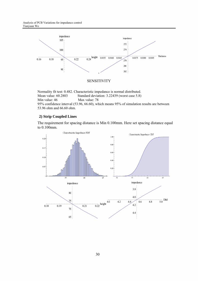
2) Strip Coupled Lines
The requirement for spacing distance is Min 0.100mm. Here set spacing distance equal to 0.100mm.
0.18 0.19 0.21 0.22height
65
70
75
80
�impedance
4.0 4.2 4.4 4.6 4.8 5.0Dk0
�4.4
�4.2
�4.0
�3.8
�impedance

Analysis of PCB Variations for impedance control Tianyuan Wo
31
0.090 0.095 0.105 0.110width
�220
�215
�210
�205
�200
�195
�impedance
0.01550.01600.0165 0.01750.01800.0185thickness
�325
�315
�310
�impedance
0.090 0.095 0.105 0.110s
26
28
30
32
34
36
�impedance
Sensitivity
Mean value: 56.13 Standard deviation: 2.19 (worst case 4.0) Min value: 44 Max value: 69 95% confidence interval (53.81, 62.43), which means 95% of simulation results are between 53.81ohm and 62.43 ohm.
Result
With the specification, the tolerances of characteristic impedance are expected:
Outer layer single line [31, 69] ohm Inner layer single line [46, 78] ohm Inner layer coupled lines [45, 69] ohm
The expected distributions are as above in this section. If supplier can provide high precision, the interval can be narrower. In order to get better accuracy, tolerance of critical variables’ mean value should also be a part of requirement. Critical variable can be defined as the variable that impedance is sensitive for. For instance, if the mean dielectric thickness of the Microstrip line was shifted from 60 um to 68 um, 95% confidence interval would change to (46, 59). The tolerance depends on how precise the result should be.
4.2 Analysis based on Multek and GCE’s data The result can be seen in the intern report. The quantity of samples is not large enough to get real distributions. The result’s reliability is based on the data supplier provided. If we set limits for the critical variables’ mean, the variation from the expected value could be reduced.

Analysis of PCB Variations for impedance control Tianyuan Wo
32
5 CONCLUSION
Controlling impedance in PCB is a complicated task. It needs tons of data to ensure the reliability. Not only PCB supplier should be responsible for final product’s quality, but also designer. Actually, Designer’s role is more important. The maximal possible deviation of impedance depends on designer’s requirement. As long as suppliers provide product with all variables falling in tolerance interval, we as designer can not reject the product. But the result could be terrible if the value of variable is very close to the tolerance interval’s edge. The possibility of extreme cases happening may be small, but still could happen.
The actual quality of the final products depends on suppliers’ accuracy and precision. Accuracy and precision are not bound to each other. Suppliers may provide high precision but low accuracy. When this happened, some extreme cases you thought should be would no longer be extreme. Suppliers will not be responsible for that; therefore designer must be very careful when set requirements to ensure their accuracy and precision.
If you are not satisfied with result’s distribution, the quickest way for designer to improve it is to narrow its tolerance interval. This can be achieved by narrowing down the critical variables’ interval. If you are satisfied with result’s precision, but want to improve the accuracy, you can set stricter requirement for the critical variables’ mean. Critical variables can be found through sensitivity study. Sensitivity study is enormously important to impedance control. It can not only tell us which variables are critical, but also tell us which combinations of variables can give relatively smaller deviation.
Suppliers should keep recording data during manufacturing. Too small amount of data can not show real distribution and be difficult for designer to analyze. It is better to provide CDF or PDF if possible. CPK value is based on normality assumption. The real distribution may not be normally distributed.
In this project, the targets are only these most basic types of transmission lines: surface single-ended microstripline, surface edge-coupled microstriplines, symmetric single-ended stripline, and edge-coupled Striplines. Other types are not included in the study, because suitable formulas were not found. Results of broadside-coupled striplines’ formula in appendix A could not meet the results from Advanced Design System (ADS). All the design jobs are based on ADS; therefore we must assume the algorithms in ADS are always correct, and a wrong formula can not be used to analyze data. However, the method to analyze other type of transmission lines is same. In future studies, people can do similar analysis if can access to the formulas that give more close results to ADS.

Analysis of PCB Variations for impedance control Tianyuan Wo
33
6 REFERENCE LIST
[1] Clayton R.Paul, (2010), Transmission Lines In Digital and Analog Electronic Systems: Signal Integrity and Crosstalk, Wiley, ISBN 978-0-470-59230-4
[2] Sawilowsky, Shlomo S; Fahoome, Gail C. (2003), Statistics via Monte Carlo Simulation with FORTRAN, Rochester Hills, ISBN 0-9740236-0-4
[3] Saltelli A., Ratto M., Andres T., Campolongo F., Cariboni J., Gatelli D., Saisana M., and Tarantola S., (2008), Global Sensitivity Analysis, The Primer, John Wiley & Sons.
[4] Istvan Nagy, How to calculate PCB trace width and differential pair separation, based on the impedance requirement and other variables.
[5] Inder Bahl and Prakash Bhartia, Microwave Solid State Circuit Design, Second Edition

Analysis of PCB Variations for impedance control Tianyuan Wo
34
7 APPENDIX A – CHARACTERISTIC IMPEDANCE EXPRESSIONS9
The tables are copied from Microwave Solid State Circuit Design, Second Edition.
9 Inder Bahl and Prakash Bhartia, Microwave Solid State Circuit Design, Second Edition

Analysis of PCB Variations for impedance control Tianyuan Wo
35

Analysis of PCB Variations for impedance control Tianyuan Wo
36
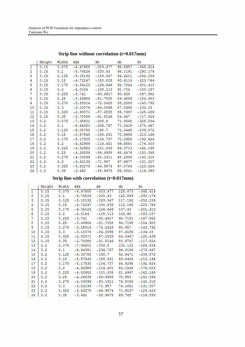
8 APPEDIX B – PARTIAL DERIVATIVES (dk=4.5)
Microstrip line without correlation (t=0.05mm)
Microstrip line with correlation (t=0.05mm)
Analysis of PCB Variations for impedance control Tianyuan Wo
37
Strip line without correlation (t=0.017mm)
Strip line with correlation (t=0.017mm)

Analysis of PCB Variations for impedance control Tianyuan Wo
38
Strip coupled lines without correlation (s=0.1mm, t=0.017mm)
Strip coupled lines with correlation (s=0.1mm, t=0.017mm)
Analysis of PCB Variations for impedance control Tianyuan Wo
39
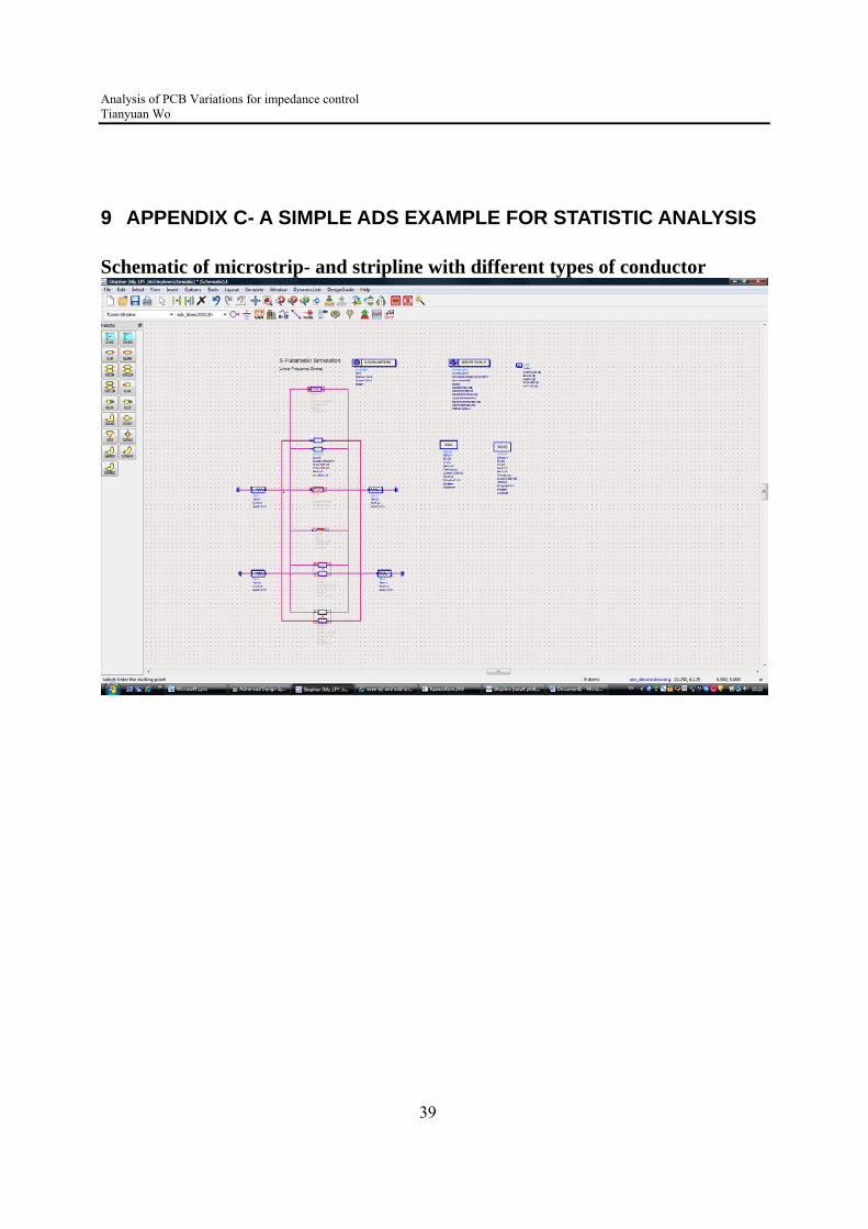
9 APPENDIX C- A SIMPLE ADS EXAMPLE FOR STATISTIC ANALYSIS Schematic of microstrip- and stripline with different types of conductor

Analysis of PCB Variations for impedance control Tianyuan Wo
40
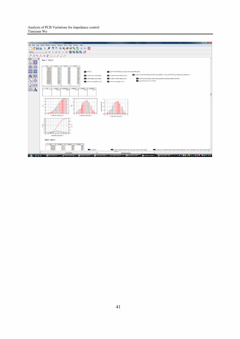
Result
Statistic analysis
Analysis of PCB Variations for impedance control Tianyuan Wo
41

www.kth.se
TRITA-ICT-EX-2012:147