analysis, design and implementation of noise shaping data...
TRANSCRIPT

2732 | P a g e
ANALYSIS, DESIGN AND IMPLEMENTATION OF
NOISE SHAPING DATA CONVERTERS FOR POWER
SYSTEMS
Maraim Asif1, Prof Pallavi Bondriya
2
1Department of Electrical and Electronics Engineering, Technocrats institute of Technology,
Bhopal, (India)
2Head Of the Department, Department of Electrical & Electronics Engineering,
Technocrats Institute of Technology, Bhopal, (India)
ABSTRACT
This paper illustrates design and simulation of noise shaping data converters, The presented approach will
enable to develop a noise shaping theory along with behavioral models to illustrate using simulations the
operation of noise shaping analog to digital converters and digital to analog converters. The objective of
designs presented this paper is to discuss the fundamentals of noise shaping data converter design and to put a
framework together for various simulations and computing methodologies. The method includes evaluating
mixed signal designs with high complexity for power systems. The architecture considered will be with unique
characteristics and limitations. The chosen architecture will also define the operating characteristics of data
converters. FFT analysis is also done for better results.
Index Terms: Data Converters, ADC, DAC, FFT Analysis, Power systems
I. INTRODUCTION (HEADING 1)
Analog-to-digital converters, also known as A/Ds or ADCs, convert analog signals to discrete time or digital
signals. Digital-to-analog converters (D/As or DACs) perform the reverse operation. Data converters comprises
of both ADCs and DACs and they are the most important integral parts of any power system. Since MOSFETS
do form the system of any modern analog, digital or any mixed signal design at a certain abstraction level, Power
MOSFETs and amplifiers made out of those will be the basis of any data converters that are exclusively meant for
signal processing. One of the most popular data converters is Delta sigma converters also known by different
names such as Oversampling ADC and most importantly noise shaping data converter. The above mentioned
name comes from the architecture of modulator which integrates the difference between the input and quantized
output.
Analog-to-digital or digital to analog converters play an essential role in modern RF receiver design.
Conventional Nyquist converters require analog components that are precise and highly immune to noise and
interference. In contrast, oversampling converters can be implemented using simple and high-tolerance analog
components. Moreover, sampling at high frequency eliminates the need for abrupt cutoffs in the analog

2733 | P a g e
antialiasing filters. [2] A technique of noise shaping is used in SD converters in addition to oversampling to
achieve a high-resolution conversion. A significant advantage of the method presented in the paper is that analog
signals are converted using simple and high-tolerance analog circuits, usually comparators, and analog signal
processing circuits having a precision that is usually much less than the resolution of the overall converter
II. NEED OF DATA CONVERTERS
Analog-to-Digital converters (ADCs) translate analog quantities, which are characteristic of most phenomena in
the real world'' to digital language, used in information processing, computing, data transmission, and control
systems Digital-to-Analog converters (DACs) are used in transforming transmitted or stored data, or the results
of digital processing back to real world variables for control, information display, or further analog processing.
Fig. 1 Signal Characteristics Changes In Analog To Digital Conversion
Fig. 2 Signal Characteristics Changes In Digital To Analog Conversion
The original analog signal is filtered by an anti-aliasing filter to remove any high-frequency components that
may cause an effect known as aliasing. The signal is sampled and held and then converted into a digital signal
.Next the DAC converts the digital signal back into an analog signal. Note that the output of the DAC is not as
"smooth" as the original signal. A low-pass filter returns the analog signal back to its original form plus phase
shift introduced from the conversions [3] after eliminating the higher order signal components caused by the
conversion. This illustrates the main differences between analog and digital signals. Whereas the analog signal
in is continuous and infinite valued, the digital signal in is discrete with respect to time and quantized.
Fig 3 Fundamental block diagram illustrating ADC and DAC
III. POWER MOSFET -USE AND BENEFITS
2734 | P a g e
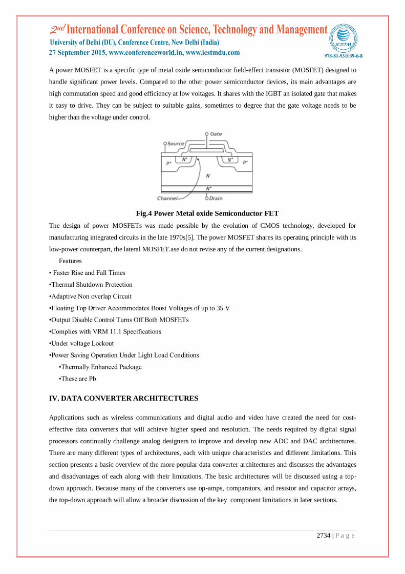
A power MOSFET is a specific type of metal oxide semiconductor field-effect transistor (MOSFET) designed to
handle significant power levels. Compared to the other power semiconductor devices, its main advantages are
high commutation speed and good efficiency at low voltages. It shares with the IGBT an isolated gate that makes
it easy to drive. They can be subject to suitable gains, sometimes to degree that the gate voltage needs to be
higher than the voltage under control.
Fig.4 Power Metal oxide Semiconductor FET
The design of power MOSFETs was made possible by the evolution of CMOS technology, developed for
manufacturing integrated circuits in the late 1970s[5]. The power MOSFET shares its operating principle with its
low-power counterpart, the lateral MOSFET.ase do not revise any of the current designations.
Features
• Faster Rise and Fall Times
•Thermal Shutdown Protection
•Adaptive Non overlap Circuit
•Floating Top Driver Accommodates Boost Voltages of up to 35 V
•Output Disable Control Turns Off Both MOSFETs
•Complies with VRM 11.1 Specifications
•Under voltage Lockout
•Power Saving Operation Under Light Load Conditions
•Thermally Enhanced Package
•These are Pb
IV. DATA CONVERTER ARCHITECTURES
Applications such as wireless communications and digital audio and video have created the need for cost-
effective data converters that will achieve higher speed and resolution. The needs required by digital signal
processors continually challenge analog designers to improve and develop new ADC and DAC architectures.
There are many different types of architectures, each with unique characteristics and different limitations. This
section presents a basic overview of the more popular data converter architectures and discusses the advantages
and disadvantages of each along with their limitations. The basic architectures will be discussed using a top-
down approach. Because many of the converters use op-amps, comparators, and resistor and capacitor arrays,
the top-down approach will allow a broader discussion of the key component limitations in later sections.

2735 | P a g e
A wide variety of DAC architectures exist, ranging from very simple to complex. Each, of course, has its own
merits. Some use voltage division, whereas others employ current steering and even charge scaling to map the
digital value into an analog quantity.
In many cases, the digital signal is not provided in binary code but is any one of a number of codes: binary,
BCD, thermometer code, Gray code, sign-magnitude, two's complement, offset binary, and so on. For example,
it may be desirable to allow only one bit to change value when changing from one code to the next. If that is the
case, a Gray code will suffice. Notice that it requires 2N- 1 bits to represent an N-bit word. The choice of code
depends on the application, and the reader should be aware that many types of codes are available.
A survey of the field of current A/D converter research reveals that a majority of effort has been directed to four
different types of architectures: pipeline, flash-type, successive approximation, and oversampled ADCs. Each
has benefits that are unique to that architecture and span the spectrum of high speed and resolution. Since the
ADC has a continuous, infinite-valued signal as its input, the important analog points on the transfer curve x-
axis for an ADC are the ones that correspond to changes in the digital output word. These input transitions
determine the amount of INL and DNL associated with the converter.
Flash or parallel converters have the highest speed of any type of ADC. Generally the use of one comparator
per quantization level (2™ - 1) and 2N resistors a resistor-string DAC). The reference voltage is divided into 2N
values, each of which is fed into a comparator. The input voltage is compared with each reference value and
results in a thermometer code at the output of the comparators. A thermometer code exhibits all zeros for each
resistor level if the value of vm is less than the value on the resistor string, and ones if vIN is greater than or
equal to voltage on the resistor string. A simple 2N -l:N digital thermometer decoder circuit converts the
compared data into an TV-bit digital word.
The obvious advantage of this converter is the speed with which one conversion can take place. Each clock
pulse generates an output digital word. The advantage of having high speed, however, is counterbalanced by the
doubling of area with each bit of increased resolution. For example, an 8-bit converter requires 255 comparators,
but a 9-bit ADC requires 511 ! Flash converters have traditionally been limited to 8-bit resolution with
conversion speeds of 10-40 Ms/s using CMOS technology. The disadvantages of the Flash ADC are the area
and power requirements of the 2N- 1 comparators. The speed is limited by the switching of the comparators and
the digital logic.
Fig.5. Popular ADC/DAC reference options[5]

2736 | P a g e
V. IMPLEMENTING DATA CONVERTERS
Technology continues to scale towards smaller dimensions. This feature size reduction is driven mainly by the
desire to implement digital systems of increased complexity in a smaller area. This natural trend in feature size
reduction, with accompanying reduction in supply voltage and poorer matching, can present challenges for the
CMOS circuit designer. The accompanying lower supply voltage, for example, results in an inherent reduction
in dynamic range, decrease in SNR, and increasing challenges when implementing analog circuitry with little,
ideally zero, voltage overhead.
This section reviews and discusses implementation methods and trade-offs for designing data converters in
nanometer CMOS. For DAC design, we focus on converters implemented with both resistors using R-2R
networks and current sources. The benefit of,and reason we are focusing on, using R-2R networks and current
sources over other methods for DAC implementation, such as charge redistribution DACs, is the absence of
good poly-poly capacitors in nanometer digital CMOS processes. R-2R-based DACs can be laid out in a small
area while achieving resolutions in excess of 10-bits without calibrations or trimming. Charge-scaling DACs
require linear capacitors. The layout area needed for these capacitors can often be very large and practically
limit both the resolution and accuracy of the DAC. It's important to note that the goal in this paper is not to
provide an exhaustive overview of data converter design but rather to provide discussions and practical insight
helpful when implementing any type of data converter in CMOS technology.
Free Devices
VI. RESULTS
Fig.6. Operational amplifier design for Data Converters
Fig.7 AC Response plot for Operational Amplifier (Operation Rage - 1 Ghz)
2737 | P a g e
Fig.8 fft for fig6 AC response
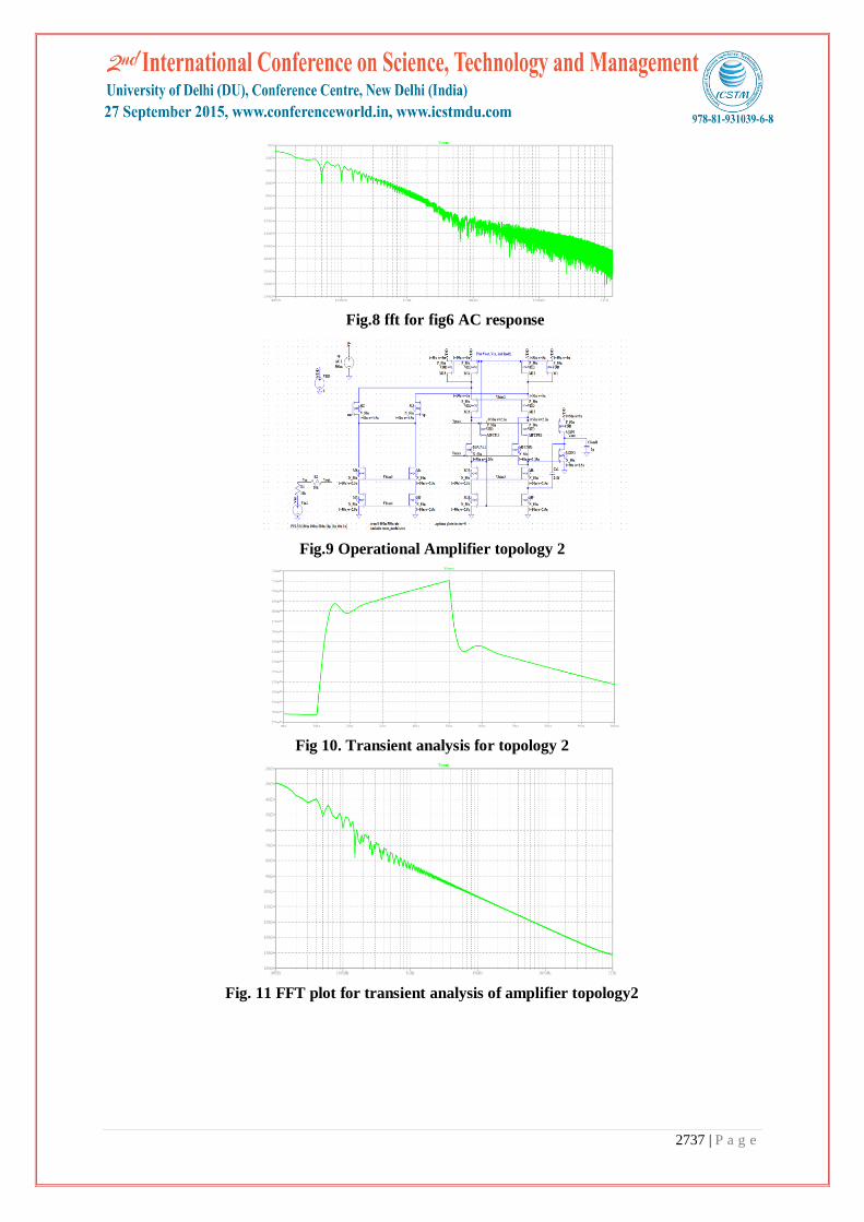
Fig.9 Operational Amplifier topology 2
Fig 10. Transient analysis for topology 2
Fig. 11 FFT plot for transient analysis of amplifier topology2

2738 | P a g e
Fig.12 Noise Analysis for Amplifier
Fig. 13 Modulator Section of Data Converter
Fig.
Fig. 14 FFT plot for modulator Section

2739 | P a g e
Fig. 15 Integrator Section of Data Convertor
Fig. 16 Analysis plot for Integrator Section with Sinusoidal input
Fig. 17 FFT plot for Output for Integrator Section with Sinusoidal input
Fig. 18 Filter Section

2740 | P a g e
Fig.19Analysis plot for Filter Section with Sinusoidal input
Fig. 20 FFT Plot for Output Filter Section
REFERENCES
[1] Hernandez, Luis, and Eladio Gutierrez. "Analytical Evaluation of VCO-ADC Quantization Noise Spectrum
Using Pulse Frequency Modulation." Signal Processing Letters, IEEE 22.2 (2015): 249-253
[2]` C.-H. Chen, Y. Zhang, J.L. Ceballos, and G. C. Temes , Noise shaping SAR ADC using three capacitors.
ISSCC 2014.
[3] R.E. Suarez, and et al.,"All-MOS charge re-distribution analog-todigital conversion techniques-Part II,"
IEEE JSSC, Dec.1985.
[4] R.Schreier and G. C. Temes, Understanding Delta-Sigma DataConverters: IEEE Press, 2005, p. 81.
[5] A. Agah, and et al., "A high-resolution low-power incremental ADC with extended range for bio-sensor
arrays," IEEE JSSC, Jun. 2010.
[6] D. Zhang, A. Bhide, and A. Alvandpour, "A 53 -nW 9.12-ENOB 1 -kS/s SAR ADC in 0.13 -um CMOS
for medical implant devices," in Proc. ESSCIRC, Sep. 2011, pp. 467-470.
[7] J. Daniels, W. Dehaene, M. Steyaert, and A. Wiesbauer, "A 0.02 mm2 65 nm CMOS 30 MHz BW all-
digital differential VCO-based ADC with 64 dB SNDR," in IEEE Symp. VLSI Circuits (VLSIC), 2010,
Jun.16-18, 2010, pp. 155-156.

2741 | P a g e
[8] J. Kim, T.-K. Jang, Y.-G. Yoon, and S. H. Cho, "Analysis and design of voltage-controlled oscillator based
analog-to-digital converter," IEEE Trans. Circuits Syst. I, vol. 57, no. 1, pp. 18-30, Jan. 2010.
[9] G. Taylor and I. Galton, "A mostly-digital variable-rate continuoustime delta-sigma modulator ADC,"
IEEE J. Solid-State Circuits, vol. 45, no. 12, pp. 2634-2646, Dec. 2010.
[10] T. Redant, P. A. J. Nuyts, P. Reynaert, and W. Dehaene, "Presilicon circuit-aware linear least squares
spectral analysis for time-based data converters," IEEE Trans. Circuits Sys. II: Exp. Briefs, vol. 60, no. 11,
pp. 751-755, Nov. 2013.
[11] C. M. Zierhofer, "Frequency modulation and first-order delta sigma modulation: Signal representation with
unity weight Dirac impulses," IEEE Signal Process. Lett., vol. 15, pp. 825-828, 2008.
[12] L. Hernández and E. Gutiérrez, "Oversampled ADC based on pulse frequency modulator and TDC,"
Electron. Lett., vol. 50, no. 7, pp. 498-499, Mar. 2014.