analog design, second course (anda) - isy.liu.se · linköping university reinventing research and...
TRANSCRIPT

Linköping University Reinventing research and education
Analog Design, second course (ANDA)
J Jacob Wikner
Electronics Systems
Department of Electrical Engineering

Lecture 1, ANDACourse introduction, CMOS basics

Analog design, second course (ANDA)
What is "analog"?
What are integrated circuits?
What is "second" course?
What is "board level", "circuit level"?
2013-01-14::ANTIK_0025 (P1A) Analog Design, second course (ANDA) 3 of 336

Web resources
WWW: http://www.es.isy.liu.se/courses/ANDA
WP: http://mixedsignal.wordpress.com
FB: http://www.facebook.com/mixedsignal
Twitter: @jjwikner
2013-01-14::ANTIK_0025 (P1A) Analog Design, second course (ANDA) 4 of 336

Studiehandboken 1
2013-01-14::ANTIK_0025 (P1A) Analog Design, second course (ANDA) 5 of 336

Studiehandboken 2
2013-01-14::ANTIK_0025 (P1A) Analog Design, second course (ANDA) 6 of 336

Studiehandboken 3
2013-01-14::ANTIK_0025 (P1A) Analog Design, second course (ANDA) 7 of 336

A brief history of time 1
Course has been around since the 1980's
Constantly evolving (you are the guinea pigs)
New for this year
Updated lessons material
Established quizzes in studiehandboken
Back to transmission line theory
More oriented towards PCB-related issues
2013-01-14::ANTIK_0025 (P1A) Analog Design, second course (ANDA) 8 of 336

Analog design, advanced course
J Jacob Wikner (Lectures, Lesson, Labs, Miniproject)
Ph.D. Linköping University, 2001Ericsson, Infineon, Sicon, Anacatum, Cognicatus, IVP, LiU
Mohammed Reza Sadeghifar (Lessons ANDA)
Ph.D. studentMaster Science, LiU
2013-01-14::ANTIK_0025 (P1A) Analog Design, second course (ANDA) 9 of 336

What is "analog" (bar voltage/current)?
A large amount of trade-offs
Design targets not as "orthogonal" as in digital design.
There are no good tools to support these trade-offs
There is no automated synthesis (c.f., the systemC/RTL-to-FPGA flow)
There is no direct porting between new processes and geometries
Plenty of guru knowledge required
2013-01-14::ANTIK_0025 (P1A) Analog Design, second course (ANDA) 10 of 336
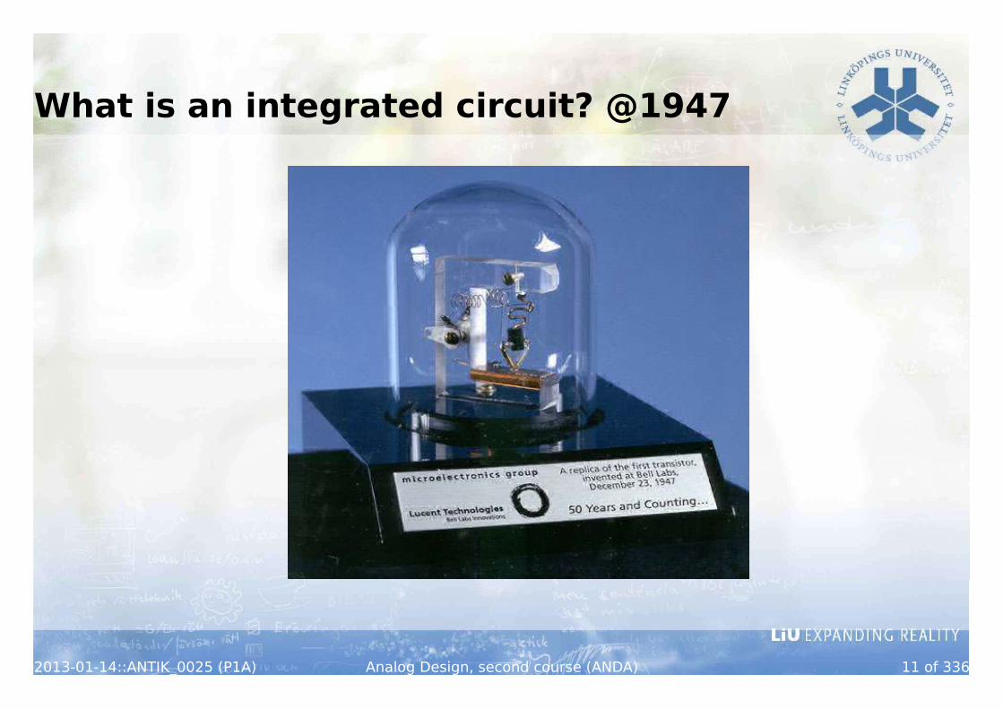
What is an integrated circuit? @1947
2013-01-14::ANTIK_0025 (P1A) Analog Design, second course (ANDA) 11 of 336

What is an integrated circuit? @1959
Courtesy of Texas Instruments
2013-01-14::ANTIK_0025 (P1A) Analog Design, second course (ANDA) 12 of 336
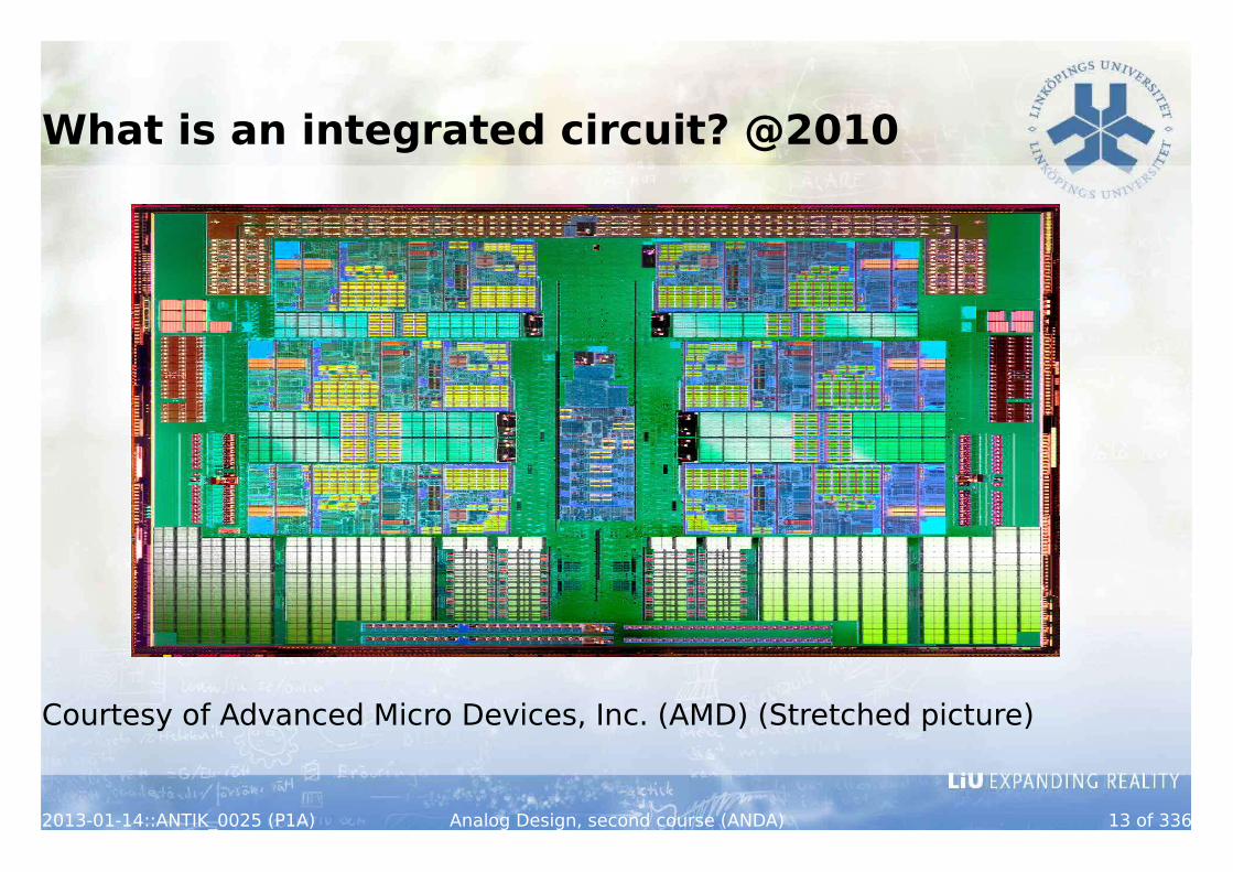
What is an integrated circuit? @2010
Courtesy of Advanced Micro Devices, Inc. (AMD) (Stretched picture)
2013-01-14::ANTIK_0025 (P1A) Analog Design, second course (ANDA) 13 of 336

What is a board-level system?
http://en.wikipedia.org/wiki/GNU_Free_Documentation_License
2013-01-14::ANTIK_0025 (P1A) Analog Design, second course (ANDA) 14 of 336
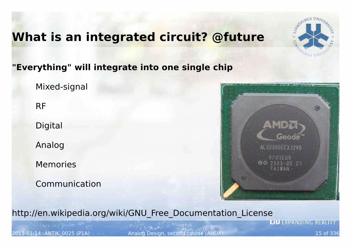
What is an integrated circuit? @future
"Everything" will integrate into one single chip
Mixed-signal
RF
Digital
Analog
Memories
Communication
http://en.wikipedia.org/wiki/GNU_Free_Documentation_License
2013-01-14::ANTIK_0025 (P1A) Analog Design, second course (ANDA) 15 of 336

A brief history of time 2
Compare with Moore's law
Every blah-blah month, the complexity doubles
Does analog scale?
With lower geometries, does analog become better - or worse?
What's the main limitation?
Cost? Physics? Law-of-nature?
2013-01-14::ANTIK_0025 (P1A) Analog Design, second course (ANDA) 16 of 336
A brief history of time ...

Course elements
Lessons follow lectures
Three Laboratories (software)
A set of computer-aided lessons
2 x 2 hours
Exam
Written exam, open-book
Quizzes
Five (best-of-three)
2013-01-14::ANTIK_0025 (P1A) Analog Design, second course (ANDA) 17 of 336

Course outline - Lectures 1
# TSEI12 ANDA
1 Introduction, MOS transistors basics and board-level basics. What does the inside of a CMOS IC look like? Basic building blocks and how do they behave from an analog point of view? What is a PCB? What is the nomenclature? What is the state of the art on this side? What does a resistor look like? Differences between PCB and silicon?
2 Analog circuits 1. Amplifiers, phase margin and stability. We start with the most basic circuits, such as single-stage amplifiers and work our way upwards. Why is in stability a problem and how to mitigate those problems.
3 Analog circuits 2. More amplifiers of different kinds. In some applications, high-speed amplifiers, or high-gain amplifiers are required and how do we design them? What to look for in data sheets when assembling.
2013-01-14::ANTIK_0025 (P1A) Analog Design, second course (ANDA) 18 of 336
Course outline - Lectures 2
# TSEI12 ANDA
4 Noise and performance measures. How accurate is "accurate"?For any system and given global specification we have to break it down into the subcomponents of our board/chip. We need to understand what cost measures to apply. We consider terms as SFDR, SNDR, INL/DNL, etc.In many applications, signal levels and required resolution are very demanding. We need to design for low-noise and wide bandwidth. How do we calculate the noise in our signal chain? How can we decouple to further reduce noise?
5 PCB vs. Silicon characteristics. Even a small board becomes big when the clock frequencies are high. Any metal strip will have a certain delay and reflections in the interconnections will also hurt the signal. How do we cope with this on a PCB? How can we prepare our circuits for these environments? What kind of tools do we have? Termination methods such as parallel- or serial termination, etc.
2013-01-14::ANTIK_0025 (P1A) Analog Design, second course (ANDA) 19 of 336
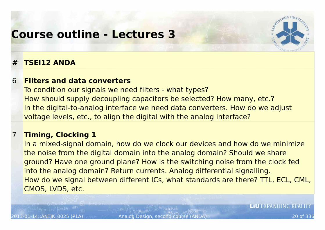
Course outline - Lectures 3
# TSEI12 ANDA
6 Filters and data convertersTo condition our signals we need filters - what types?How should supply decoupling capacitors be selected? How many, etc.?In the digital-to-analog interface we need data converters. How do we adjust voltage levels, etc., to align the digital with the analog interface?
7 Timing, Clocking 1In a mixed-signal domain, how do we clock our devices and how do we minimize the noise from the digital domain into the analog domain? Should we share ground? Have one ground plane? How is the switching noise from the clock fed into the analog domain? Return currents. Analog differential signalling. How do we signal between different ICs, what standards are there? TTL, ECL, CML, CMOS, LVDS, etc.
2013-01-14::ANTIK_0025 (P1A) Analog Design, second course (ANDA) 20 of 336

Course outline - Lectures 4
# TSEI12 ANDA
8 Other aspects. SummaryAdvanced clocking - PLL and DLL, asynchronous protocols. ESD. Q & A. Summary
A Invited lecture 1(if time and schedule permits)
B Invted lecture 2(if time and schedule permits)
2013-01-14::ANTIK_0025 (P1A) Analog Design, second course (ANDA) 21 of 336

Laboratory
Three software labs (compulsory attendance)
CMOS amplifiers (including introduction to the Cadence environment)
Decoupling capacitors
Termination and transmission lines
Computer-aided lessons (towards the end of the course)
Solving problems together with the computer
2013-01-14::ANTIK_0025 (P1A) Analog Design, second course (ANDA) 22 of 336

Exam
Open-book exam
!!!
All material can be brought to the exam
No calculators
Five exercises á five points
Be strategic
Pick your exercises
2013-01-14::ANTIK_0025 (P1A) Analog Design, second course (ANDA) 23 of 336

Quizzes
Five random questions distributed
One point on each
Maximum three points that can be accounted for in the exam
Valid for three exam occasions (March, June, August)
You will get instant feedback
2013-01-14::ANTIK_0025 (P1A) Analog Design, second course (ANDA) 24 of 336

Quiz example
In a common-source amplifier, to minimize the output-referred noise, how should you design the transconductance of the active load?
1) To be as high as possible
2) To be as low as possible
3) The active load does not add noise to the output
2013-01-14::ANTIK_0025 (P1A) Analog Design, second course (ANDA) 25 of 336
V i n
V outV b
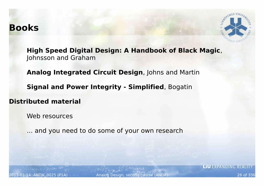
Books
High Speed Digital Design: A Handbook of Black Magic, Johnsson and Graham
Analog Integrated Circuit Design, Johns and Martin
Signal and Power Integrity - Simplified, Bogatin
Distributed material
Web resources
... and you need to do some of your own research
2013-01-14::ANTIK_0025 (P1A) Analog Design, second course (ANDA) 26 of 336
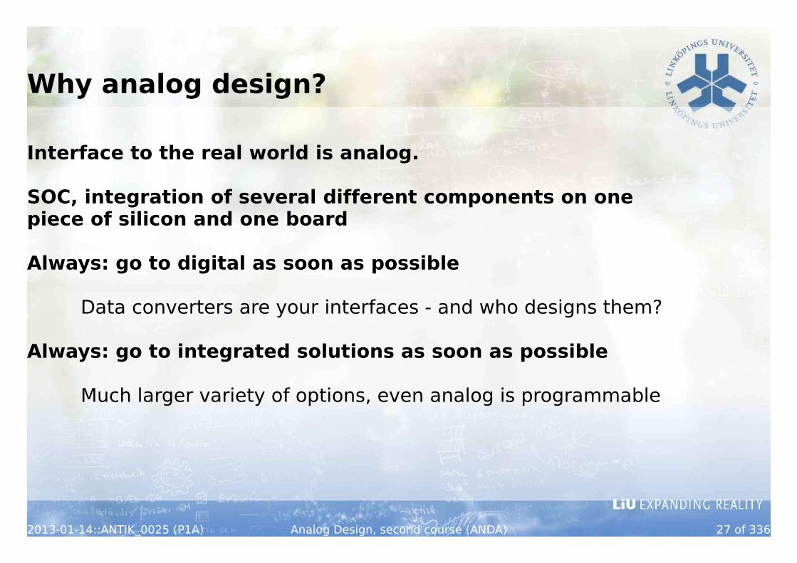
Why analog design?
Interface to the real world is analog.
SOC, integration of several different components on one piece of silicon and one board
Always: go to digital as soon as possible
Data converters are your interfaces - and who designs them?
Always: go to integrated solutions as soon as possible
Much larger variety of options, even analog is programmable
2013-01-14::ANTIK_0025 (P1A) Analog Design, second course (ANDA) 27 of 336

Where could this lead?
Linköping master thesis at the CES 2012 (Las Vegas)
Fingerprints strikes a deal with Tier 1
Signal Processing Devices AB
AnaCatum Design AB
... and more ...
2013-01-14::ANTIK_0025 (P1A) Analog Design, second course (ANDA) 28 of 336

Zzzzzzz, zzzz - get to the point!
2013-01-14::ANTIK_0025 (P1A) Analog Design, second course (ANDA) 29 of 336
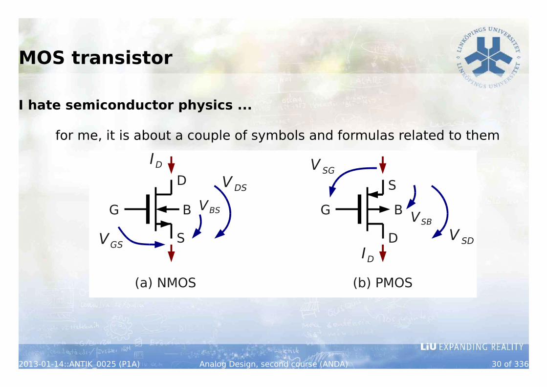
MOS transistor
I hate semiconductor physics ...
for me, it is about a couple of symbols and formulas related to them
2013-01-14::ANTIK_0025 (P1A) Analog Design, second course (ANDA) 30 of 336
D
S
G B
D
S
G B
ID
ID
V DS
VBS
VGS
V SG
VSB
V SD
(a) NMOS (b) PMOS

The physical aspects
"Planar" technology
Operations
Saturation
Linear
Off
Capacitive effects
etc, etc
2013-01-14::ANTIK_0025 (P1A) Analog Design, second course (ANDA) 31 of 336

The regions
Subthreshold(cut-off)
Linear(low gain)
Saturation(high gain)
I≈0 I≈α⋅(2V eff V ds−V ds2 ) I≈αV eff
2
V eff<0 V eff>0 , V ds<V eff V eff>0 , V ds>V eff
2013-01-14::ANTIK_0025 (P1A) Analog Design, second course (ANDA) 32 of 336


The second-order effects
Subthreshold Linear Saturation
I≈ I D0⋅eV eff
k T /q I≈α⋅(2V eff V ds−V ds2 ) I≈αV eff
2⋅(1+V ds
V θ)
V T=V T0+γ⋅(√2ΦF−V BS−√2ΦF ) , V θ=1 /λ
2013-01-14::ANTIK_0025 (P1A) Analog Design, second course (ANDA) 34 of 336
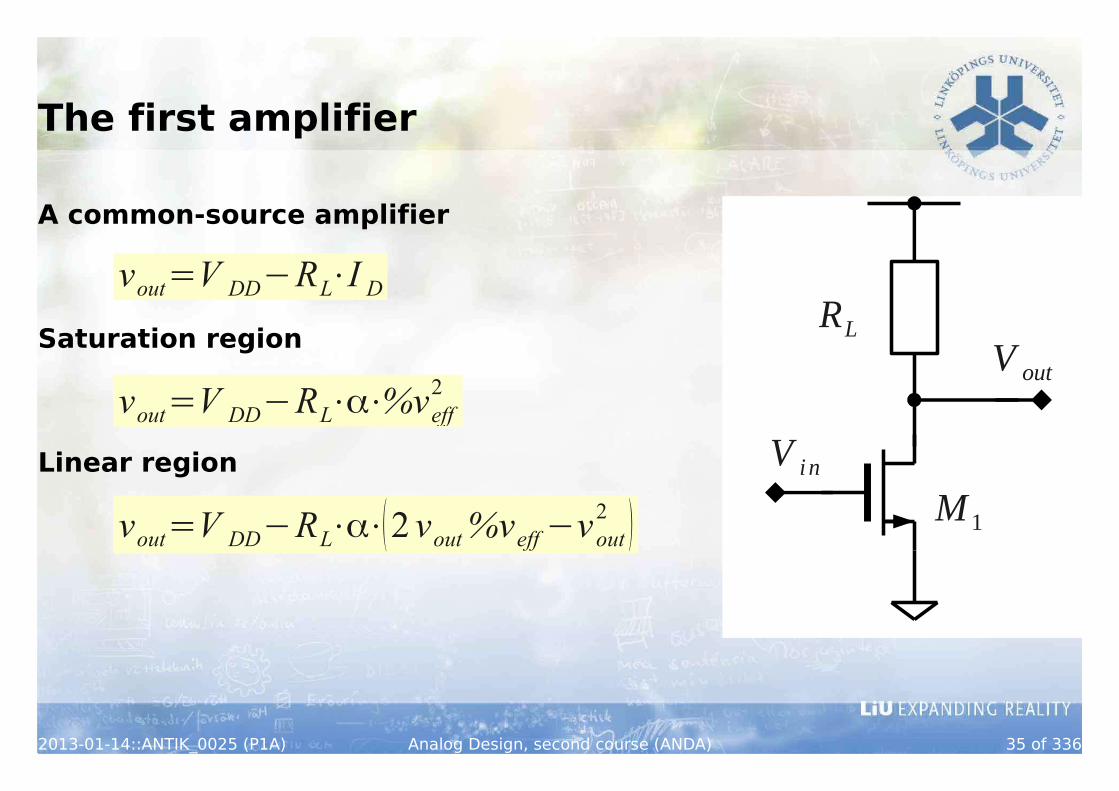
The first amplifier
A common-source amplifier
vout=V DD−RL⋅I D
Saturation region
vout=V DD−RL⋅α⋅%veff2
Linear region
vout=V DD−RL⋅α⋅(2 vout%veff−vout2 )
2013-01-14::ANTIK_0025 (P1A) Analog Design, second course (ANDA) 35 of 336
V i n
V out
RL
M 1

A simple testbench
2013-01-14::ANTIK_0025 (P1A) Analog Design, second course (ANDA) 36 of 336


The second order effects
2013-01-14::ANTIK_0025 (P1A) Analog Design, second course (ANDA) 38 of 336
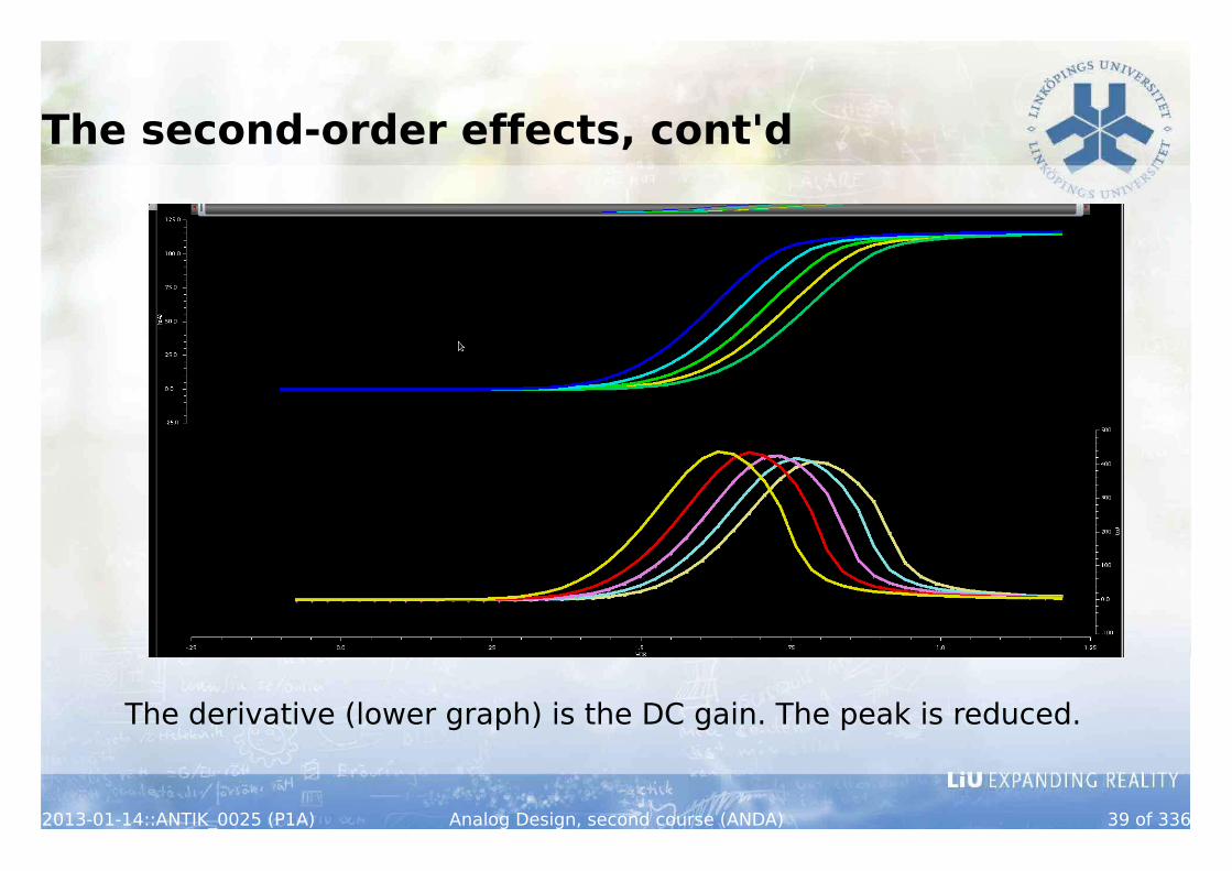
The second-order effects, cont'd
The derivative (lower graph) is the DC gain. The peak is reduced.
2013-01-14::ANTIK_0025 (P1A) Analog Design, second course (ANDA) 39 of 336

Board activities ...
The large-signal scenario
Continued
The small-signal scenario
(Next lecture)
Design centering
Operating point
2013-01-14::ANTIK_0025 (P1A) Analog Design, second course (ANDA) 40 of 336

What did we do today?
Introduction to the course
Labs, quizzes, exam, etc.
The transistor
Operating regions
Functionality
First amplifier and parameters
A starting point for the lessons
2013-01-14::ANTIK_0025 (P1A) Analog Design, second course (ANDA) 41 of 336

What will we do next time?
Small-signal schematics
Linearization
Further work on the analog building blocks
Common-source, common-drain, common-gate, etc.
Stability and why
2013-01-14::ANTIK_0025 (P1A) Analog Design, second course (ANDA) 42 of 336