analog circuits, second course (anda) - linköping … · title analog circuits, second course...
TRANSCRIPT
No Rev Date Repo/Course Page
0030 A 2013-02-26 ANTIK 1 of 62
Title Analog Circuits, Second Course (ANDA)
File ANTIK_0030_LM_andaLabManual_A.odt
Type LM -- Laboratory Manual Area es : docs : courses : antik
Created J Jacob Wikner Approved J Jacob Wikner
Issued J Jacob Wikner, jacwi50 Class Public
Laboratory Manual
Analog Circuits, Second Course (ANDA)
Description
The purpose of this laboratory exercise is to mainly provide the student with hands-on experience of the Cadence design tools used in the ANTIK courses, i.e., Analog and Discrete-Time Integrated Circuits (ATIK) and Analog Circuits, Second course (ANDA).
Notice that the first few sections are introductory to Cadence. The experienced Cadence user could skip these. BUT! This lab also uses the so-called daisy flow which is a shell around Cadence and some vital information about it is found in the first sections.
Also notice that the labs are not focusing on a lot of fill-in-the-box-so-that-I-can-go-home exercises. Instead some of the questions are found in the text flow and some of the questions cannot be answered just with a number or so.
✗ Read the instructions carefully.
✗ A suggested outline of the labs vs chapter of this monologue is found in Section 0.2. It is up to the student to distribute his time.
Preparation exercises are marked as for example:
Derive the small-signal model for the circuit in Figure 1.2. Derive the input and output impedances, the DC gain, and the bandwidth. !
Do these before you show up at the lab!
This document is released by Electronics Systems (ES), Dep't of E.E., Linköping University. Repository refers to ES Print Date: 02/26/13, 08:46
No Rev Date Repo/Course Page
0030 A 2013-02-26 ANTIK 2 of 62
Title Analog Circuits, Second Course (ANDA) ID jacwi50
Outline
-LAB0- Overview/ Introduction/ Instructions .............................................................................6
Lab 0.1 - Introduction..............................................................................................................6Lab 0.2 - Instructions for the students....................................................................................7Lab 0.3 - Initiating your Linux environment............................................................................7Lab 0.4 - Getting started with Cadence and Daisy flow..........................................................9Lab 0.5 - Simulating a circuit schematic...............................................................................14Lab 0.6 - An example circuit ................................................................................................17
-LAB1- Single-stage Amplifiers................................................................................................27
Lab 1.1 - Introduction............................................................................................................27Lab 1.2 - CMOS gain stages..................................................................................................31Lab 1.3 - Transient simulation .............................................................................................34
-LAB2- Transmission lines and termination.............................................................................37
Lab 2.1 - Introduction............................................................................................................37Lab 2.2 - Preparations...........................................................................................................38Lab 2.3 - Transmission lines and termination.......................................................................38Lab 2.4 - Impedance matching.............................................................................................41Lab 2.5 - Differential signals and return path.......................................................................45Lab 2.6 - Splitted wires..........................................................................................................48
-LAB3- Decoupling capacitors and supply filters.....................................................................50
Lab 3.1 - Introduction............................................................................................................50Lab 3.2 - Decoupling capacitors............................................................................................51Lab 3.3 - Impedance levels of decoupling capacitors...........................................................53Lab 3.4 - Taking the chip, regulator and loading effects into account..................................58
This document is released by Electronics Systems (ES), Dep't of E.E., Linköping University. Repository refers to ES Print Date: 02/26/13, 08:46
No Rev Date Repo/Course Page
0030 A 2013-02-26 ANTIK 3 of 62
Title Analog Circuits, Second Course (ANDA) ID jacwi50
List of Tables
Table 0.1: List of cells that are useful for this lab......................................................................12Table 0.2: Examples on useful shortcut keys (bind keys).........................................................14Table 0.3: Example on DC results options.................................................................................16Table 0.4: Example on some useful calculator commands.......................................................17Table 0.5: Example of pin placements......................................................................................19Table 0.6: Parameters for the pulse source in the first test bench............................................21Table 0.7: Design variables in the first test bench....................................................................23Table 0.8: Examples on simulated performance and some “typical” values for this process.. .24Table 0.9: Performance parameters for CS amplifier................................................................24Table 0.10: Simulation observations.........................................................................................25Table 0.11: A list of some useful Daisy bind-keys.....................................................................26Table 1.1: Simulated DC gain and -3dB frequency with original DC level.................................29Table 1.2: Simulated DC gain and -3dB frequency with new DC level.......................................29Table 1.3: Specification on single-stage active buffer/amplifiers..............................................33Table 1.4: vpulse values............................................................................................................34Table 1.5: Simulated results for the single-stage amplifiers.....................................................36Table 3.1: Components of a decoupling capacitor....................................................................53Table 3.2: Standard series of capacitor values.........................................................................56
This document is released by Electronics Systems (ES), Dep't of E.E., Linköping University. Repository refers to ES Print Date: 02/26/13, 08:46
No Rev Date Repo/Course Page
0030 A 2013-02-26 ANTIK 4 of 62
Title Analog Circuits, Second Course (ANDA) ID jacwi50
List of Figures
Figure 0.1: Illustration of how to add a design variable name..................................................11Figure 0.2: The common source amplifier with an NMOS as input device.................................19Figure 0.3: The symbol of a common-source amplifier.............................................................20Figure 0.4: The test bench of the common source amplifier.....................................................22Figure 1.1: Transistor view of single-stage common-source amplifier......................................28Figure 1.2: Transistor view of single-stage amplifier stages with active loads; common source (a), common drain (b), and common gate (c). ...............................................32Figure 2.1: First trial including a voltage source ("port"), a transmission line, and a termination resistor...................................................................................................................................... 42Figure 2.2: Termination including an unmatched ground plane...............................................45Figure 2.3: A splitted wire with different transmission line properties......................................48Figure 3.1: Model of a decoupling capacitor..............................................................................52Figure 3.2: Example of a power network showing a model of the regulator, the ground plane, the supply impedance, the decoupling capacitors, and the switching active circuits...............58Figure 3.3: Example of an impedance plot. ..............................................................................60
This document is released by Electronics Systems (ES), Dep't of E.E., Linköping University. Repository refers to ES Print Date: 02/26/13, 08:46
No Rev Date Repo/Course Page
0030 A 2013-02-26 ANTIK 5 of 62
Title Analog Circuits, Second Course (ANDA) ID jacwi50
History
Rev Date Comment Created/Issued by
P1A 2013-01-09 Updated for the new labs in the TSEI12 version of the course. New document number and title. Reduces the contents of lab 1 quite significantly. Illustrated lab 0 a bit more clearly.
J Jacob Wikner
P2A 2013-02-12 Updated the transmission-line lab and the decoupling caps lab.
J Jacob Wikner
P3A 2013-02-13 "Finalized" lab 2. Handed over to Niklas for a second pair of eyes.
J Jacob Wikner
P4A 2013-02-15 Working copy. Released lab 0, lab 1, and lab 2. J Jacob Wikner
P5A 2013-02-18 Corrected some of the typos in the second lab. J Jacob Wikner
P6A 2013-02-25 Updated the lab manual with the decoupling lab parts.
J Jacob Wikner
A 2013-02-26 Finalized all labs. Removed the current-mirror part. Release for 2013.
J Jacob Wikner
This document is released by Electronics Systems (ES), Dep't of E.E., Linköping University. Repository refers to ES Print Date: 02/26/13, 08:46
No Rev Date Repo/Course Page
0030 A 2013-02-26 ANTIK 6 of 62
Title Analog Circuits, Second Course (ANDA) ID jacwi50
-LAB0-
OVERVIEW/
INTRODUCTION/
INSTRUCTIONS
Lab 0.1 - Introduction
The objective with these laboratories is to provide an insight in the design procedures of analog circuits as well as using circuit simulators to understand the characteristic behaviour of a few different analog circuits.
Although it may be somewhat frustrating, some of the specifications found in this laboratory cannot be met, or at least can be very difficult to meet. (Un)fortunately, this is a good way to see how far you can push the limits, and to understand the basic limitations for the analog building blocks.
If a specification cannot be met, you should explain why and then relax the specification, redesign and try to meet your new specification. It might also be that the specification cannot be met for the chosen architecture, and then you need to learn how to argue for another architecture or another system solution.
This document is released by Electronics Systems (ES), Dep't of E.E., Linköping University. Repository refers to ES Print Date: 02/26/13, 08:46
No Rev Date Repo/Course Page
0030 A 2013-02-26 ANTIK 7 of 62
Title Analog Circuits, Second Course (ANDA) ID jacwi50
Lab 0.2 - Instructions for the students
Notice that the first lab of this document is called -LAB0- and is an introductory for those who have not worked with cadence. -LAB1- is then the first actual lab which focuses on CMOS circuit design. Then, after that, we have -LAB2- and -LAB3-, which deal with transmission lines and decoupling capacitors, respectively.
Some of the sub-exercises are marked “optional” and can be solved if you have time/interest.
Lab 0.3 - Initiating your Linux environment
The tools used in the laboratory are from the vendor Cadence Design Systems. An introduction on how to run these tools is given in this manual as well. The Cadence tool suite contains many different tools, such as component simulators, integrated circuit layout tool, physical verification, logical verification, and so on. For this lab, we will only consider the circuit-level simulation package (including a schematic capture program and a simulation environment).
When a circuit is created as a graphical netlist (schematic view), different types of circuit simulators can be used, for example HSPICE, Spectre, and SpectreS. The circuit simulators offer several types of analyses, such as DC, AC, transient, noise, etc. The speed and accuracy of the simulations also vary between the simulators. In this laboratory, the Cadence Spectre simulator is used.
We start the exercise by setting up your linux environment. Load the course module (same for both ANTIK courses):
module load ANTIK
Run a shell script to create a new directory in your home account:
cd $HOME
daisyCreateProj.sh ANTIK
✗ Only run this script once, the very first time you work with this lab! Although low risk, you might loose data if you run it eventhough you have an existing project directory.
This shell script will create a directory in your home directory called ANTIK (this is also what we from now on refer to as your work area, or $WORKAREA = $HOME/ANTIK). Further on, it will inside that directory create some other directories as well as links to files and directories. For now, you do not have to worry too much about them.
Source a dot file that was created by the script above:
This document is released by Electronics Systems (ES), Dep't of E.E., Linköping University. Repository refers to ES Print Date: 02/26/13, 08:46
No Rev Date Repo/Course Page
0030 A 2013-02-26 ANTIK 8 of 62
Title Analog Circuits, Second Course (ANDA) ID jacwi50
cd $HOME
source ~/.ANTIK_rc
✗ (Contact the lab responsible if this results in any errors or strange warning messages).
Go to the work area $WORKAREA (~/ANTIK) by typing:
cde
Now, in the $WORKAREA directory you will find a couple of links to daisyProjSetup in which you can find, for example, course information. There is a link to andaLab in which you find lab simulation files, etc. In your $WORKAREA you also find a work_$USER directory in which you should put all your personal files related to the lab and project.
Launch the Cadence design framework by typing:
cad
So, next time you log on, do the following steps and do not run the shell setup script above:
module load ANTIK
source ~/.ANTIK_rc
cad
✗ A tip! You can of course edit the dot-file and add the module load ANTIK command at the top and the cad command at the bottom. Next time you log on you only need to source the dot-file to get going.
For the lab, you may find the help from additional tools like MATLAB and Mathematica for computations of, for example, the small-signal transfer functions. (We will come back to this in the computer-aided lesson). Mathematica is a powerful tool when you want to derive an analytical expression to a given circuit topology. From the course download pages you will find some links to lazy dogs for Mathematica and Maple:
http://www.es.isy.liu.se/courses/ANDA/download/
This document is released by Electronics Systems (ES), Dep't of E.E., Linköping University. Repository refers to ES Print Date: 02/26/13, 08:46
No Rev Date Repo/Course Page
0030 A 2013-02-26 ANTIK 9 of 62
Title Analog Circuits, Second Course (ANDA) ID jacwi50
Lab 0.4 - Getting started with Cadence and Daisy flow
Once you have loaded the module, sourced the file dot file, and run the cad command you will find the CIW (command interpreter window) where information about what you are doing, errors and warning messages will be displayed. It is also commonly used for enter script-based commands. All subwindows and data are accessible through this window. Another important window, the Library Manager, is started by Tools > Library Manager... or by pressing Alt + End.
✗ Cadence is a computer software - it can crash now and then. If that happens, go to your terminal window and kill the process. Often you will get a panic.log file in your home directory which can be used to recover data. Ask the laboratory assistant to help you.
From the Library Manager, you can select which circuit you would like to work with. When you start Cadence, the Library Manager will display several different libraries. The libraries, used in these exercises, are analogLib, daisy, andaLab (1,2,3), andaLabTest, and your own design libraries (you will create them shortly).
The library analogLib contains ideal components like voltage sources, current sources, capacitors, etc. The daisy library contains some other useful components such as differential-to-single ended converters, etc.
Lab 0.4.1 - Creating a design library
When you, for example, start a new project you need to create a new library (in some sense also a new linux directory) that normally is linked to a specific design process. In these labs we use a generic CMOS process instead of a commercially available one, gpdk045.
Go to the library manager and select File > New > Library. Browse to your work area (double click on the items in the small file manager window) such that you parse to:
$WORKAREA/work_$USER/oa
(so for example /home/stdnt123/ANTIK/work_stdnt123/oa). Enter a name for the new library and press OK. Before you press return - read this:
✗ Please choose relevant names on your design library. Do not choose pointless name like:
DesignWhy not
andaWorkor something like that.
This document is released by Electronics Systems (ES), Dep't of E.E., Linköping University. Repository refers to ES Print Date: 02/26/13, 08:46
No Rev Date Repo/Course Page
0030 A 2013-02-26 ANTIK 10 of 62
Title Analog Circuits, Second Course (ANDA) ID jacwi50
A new dialogue window will appear where you should select a technology to attach to your library. Select Attach to an existing techfile and press OK. Choose Technology gpdk045 and press OK. Now you have a new library in which you can start creating your cells.
Lab 0.4.2 - Creating a cell view
Select the design library in which you like to add your new cell view. From the library manager, select File > New > Cell View. Enter a cell name and choose a tool/application.
✗ Notice that the popup windows tend to end up behind other windows on the Desktop.
For these labs we will choose between these two tools:
• Schematic L to design a circuit in the schematics mode.
• Symbol L to create symbols for a schematic to be used in hierarchical designs.
✗ You can choose (almost) any name in the Cell name, but use “schematic” or “symbol” or the View. This is normally automatically chosen if you select the tool above. Aslo make sure to not use any silly characters like “$”, “/”, etc.
The tool you have selected will then be loaded and you can start designing the circuit.
✗ It is a good practice to also inherit the library name in the cell name, for exampleandaLab / andaLabInverterThis is for compatibility with other tool vendors, where the design libraries are treated a bit differently, and also in a spice netlist file, the hierarchy does not exist in the same way as it does in the Cadence database.
Lab 0.4.3 - Schematic
The schematic composer is a graphical interface to define the netlist of a circuit. From the schematic view, a netlist can be generated such that we can run simulations on them to perform and evaluate the performance of the sized circuit. Normally, the simulator uses very accurate device models, but typically from the schemtic level, there is no additional information from, e.g., wire capacitance or resistance extracted. These factors depend on the layout, but to add them to the simulations we first need to lay out our circuit and extract it with a layout-level extraction tool.
This document is released by Electronics Systems (ES), Dep't of E.E., Linköping University. Repository refers to ES Print Date: 02/26/13, 08:46
No Rev Date Repo/Course Page
0030 A 2013-02-26 ANTIK 11 of 62
Title Analog Circuits, Second Course (ANDA) ID jacwi50
Fetching an element to be used in the schematic
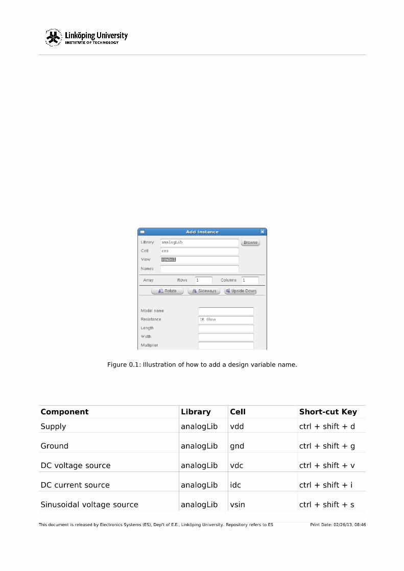
Elements such as voltage sources, transistors, and capacitors are predefined building blocks that can be inserted in the schematic by either Create > instance or by pressing the bind-key 'i'. A subwindow will appear (Figure 0.1) where you can add a component by specifying the library, cell and view, as well as parameters associated with it. The view should normally be a symbol. You can either add a predefined cell for example the ones listed in Table 0.1, or a component for which you have created a symbol of your own.
When a component is chosen to be placed in the schematic, by either writing the names of the libraries and the cell view, or by using the browse button, the properties of the selected components will appear further down in the Add instance window (Figure 0.1). For example, the width and length of a transistor, or the DC level of a voltage source, etc.
No Rev Date Repo/Course Page
0030 A 2013-02-26 ANTIK 12 of 62
Title Analog Circuits, Second Course (ANDA) ID jacwi50
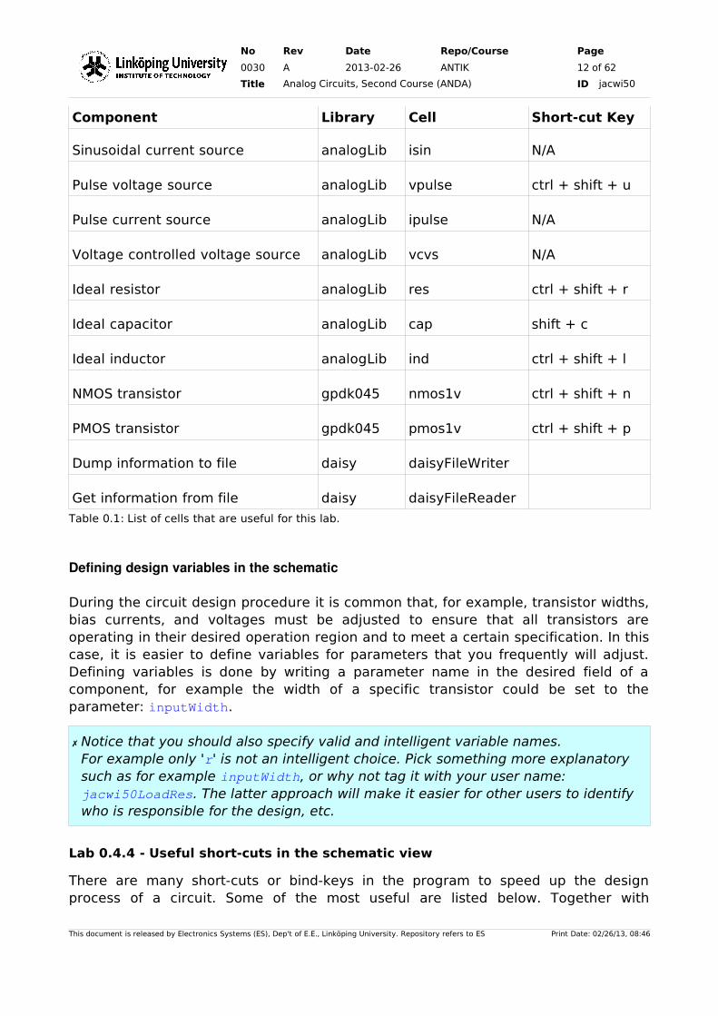
Component Library Cell Short-cut Key
Sinusoidal current source analogLib isin N/A
Pulse voltage source analogLib vpulse ctrl + shift + u
Pulse current source analogLib ipulse N/A
Voltage controlled voltage source analogLib vcvs N/A
Ideal resistor analogLib res ctrl + shift + r
Ideal capacitor analogLib cap shift + c
Ideal inductor analogLib ind ctrl + shift + l
NMOS transistor gpdk045 nmos1v ctrl + shift + n
PMOS transistor gpdk045 pmos1v ctrl + shift + p
Dump information to file daisy daisyFileWriter
Get information from file daisy daisyFileReader
Table 0.1: List of cells that are useful for this lab.
Defining design variables in the schematic
During the circuit design procedure it is common that, for example, transistor widths, bias currents, and voltages must be adjusted to ensure that all transistors are operating in their desired operation region and to meet a certain specification. In this case, it is easier to define variables for parameters that you frequently will adjust. Defining variables is done by writing a parameter name in the desired field of a component, for example the width of a specific transistor could be set to the parameter: inputWidth.
✗ Notice that you should also specify valid and intelligent variable names.For example only 'r' is not an intelligent choice. Pick something more explanatory such as for example inputWidth, or why not tag it with your user name: jacwi50LoadRes. The latter approach will make it easier for other users to identify who is responsible for the design, etc.
Lab 0.4.4 - Useful short-cuts in the schematic view
There are many short-cuts or bind-keys in the program to speed up the design process of a circuit. Some of the most useful are listed below. Together with
This document is released by Electronics Systems (ES), Dep't of E.E., Linköping University. Repository refers to ES Print Date: 02/26/13, 08:46
No Rev Date Repo/Course Page
0030 A 2013-02-26 ANTIK 13 of 62
Title Analog Circuits, Second Course (ANDA) ID jacwi50
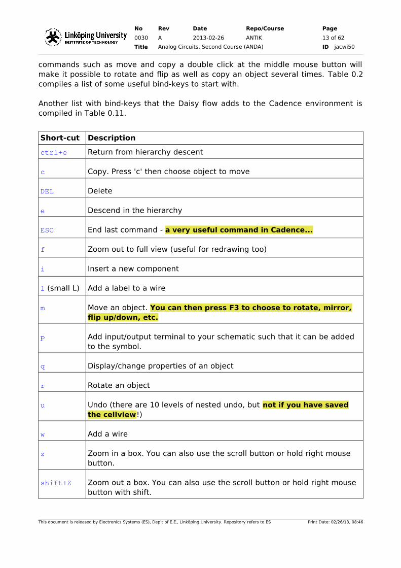
commands such as move and copy a double click at the middle mouse button will make it possible to rotate and flip as well as copy an object several times. Table 0.2 compiles a list of some useful bind-keys to start with.
Another list with bind-keys that the Daisy flow adds to the Cadence environment is compiled in Table 0.11.
Short-cut Description
ctrl+e Return from hierarchy descent
c Copy. Press 'c' then choose object to move
DEL Delete
e Descend in the hierarchy
ESC End last command - a very useful command in Cadence...
f Zoom out to full view (useful for redrawing too)
i Insert a new component
l (small L) Add a label to a wire
m Move an object. You can then press F3 to choose to rotate, mirror, flip up/down, etc.
p Add input/output terminal to your schematic such that it can be added to the symbol.
q Display/change properties of an object
r Rotate an object
u Undo (there are 10 levels of nested undo, but not if you have saved the cellview!)
w Add a wire
z Zoom in a box. You can also use the scroll button or hold right mouse button.
shift+Z Zoom out a box. You can also use the scroll button or hold right mouse button with shift.
This document is released by Electronics Systems (ES), Dep't of E.E., Linköping University. Repository refers to ES Print Date: 02/26/13, 08:46
No Rev Date Repo/Course Page
0030 A 2013-02-26 ANTIK 14 of 62
Title Analog Circuits, Second Course (ANDA) ID jacwi50
Short-cut Description
shift+Y Save whole hierarchy
shift+X Save current cellview
Table 0.2: Examples on useful shortcut keys (bind keys)
Lab 0.5 - Simulating a circuit schematic
The simulations can graphically be defined and run from the Analog Design Environment (ADE), which is started by Launch > ADE L from the schematic editing window. (You should start the simulation environment from the window which contains your top-level design, i.e., your test bench, see for example section Lab-0.6.3). As stated earlier, the simulation environment can use different types of simulators. The functionality, i.e., the types of analysis method, speed, and approximation methods when solving the system of differential equations, differ between the simulators. Analysis methods that can be used are, for example, DC analysis, small-signal analysis, transient analysis, different type of noise analysis, distortion analysis, and sensitivity analysis. In the laboratories, we will use the three most commonly used analysis methods namely DC, AC, and transient analysis.
The simulation setup can be divided into three parts: analyses, setup of the output signals, and setup of design variables.
Lab 0.5.1 - Analyses setup
DC
The DC analysis is like the one in Spice, you can either check the DC behaviour of the circuit and check that your components are operating correctly, i.e., all transistors are operating in the correct operation region and so on. Here you can for example sweep a parameter like the bias current in your amplifier to find the currents where the transistors are operating in saturation region for highest gain.
AC
The properties of the circuit with respect to a small change in the DC operating point can be evaluated by linearising the transistors around the DC operation point. This linearisation as well as the simulation of the linearised circuit is performed in the AC analysis.
This document is released by Electronics Systems (ES), Dep't of E.E., Linköping University. Repository refers to ES Print Date: 02/26/13, 08:46
No Rev Date Repo/Course Page
0030 A 2013-02-26 ANTIK 15 of 62
Title Analog Circuits, Second Course (ANDA) ID jacwi50
Transient
The transient analysis is used when the time response of a circuit is of interest. This analysis method takes into account clipping or compression of the signals, i.e., we can simulate distortion. This cannot be done in AC analysis.
Parametric analyses
Parametric analyses are used when two or more parameters are to be swept independently of each other. For example, the current into a current mirror and the width of the output transistor. In this case sweep the current in the DC analysis and add a parametric sweep using the menu alternative in the ADE: Tools > Parametric Analysis. Enter the name of the variable for the output transistor width into the field Variable Name. Add the ranges of the sweep and start the analysis by selecting Analysis > Start.
Defining output signals
The output results of the simulation can, for example, be the output voltage waveform from an amplifier, the current through a current mirror, or a mathematically defined function to calculate the unity-gain frequency of a circuit. These outputs can be selected from the schematic by using the menu command Outputs > To Be Plotted > Select On Schematic and then select the output to be plotted each time you do a simulation. Note that by selecting a wire, the node voltage for that node will be plotted, by selecting a node, the current through that node will be plotted.
Define design variables
The variables defined in the schematic view can be imported into the simulation environment. This is done by using the menu alternative Variables > Copy from Cellview.
All the variables now appear in the variable field in the ADE. To assign a value to one of the parameters just double click on the variable and enter the desired value (do not forget Apply).
Lab 0.5.2 - Results
The DC operation conditions of a circuit are computed when a DC simulation has been performed. If you like to display the result directly in the schematic use the menu alternative Result >Annotate > ...
If you like to display a complete list of the operation condition use Result > Print > ...
This document is released by Electronics Systems (ES), Dep't of E.E., Linköping University. Repository refers to ES Print Date: 02/26/13, 08:46
No Rev Date Repo/Course Page
0030 A 2013-02-26 ANTIK 16 of 62
Title Analog Circuits, Second Course (ANDA) ID jacwi50
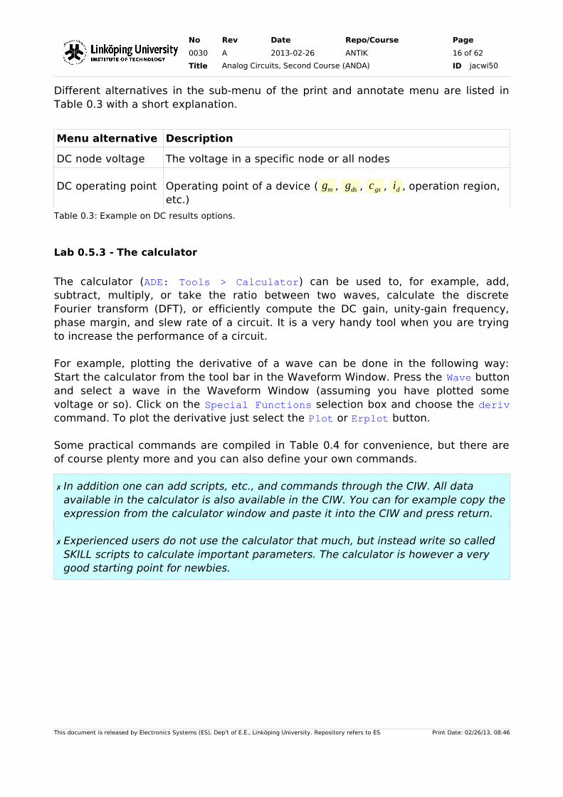
Different alternatives in the sub-menu of the print and annotate menu are listed in Table 0.3 with a short explanation.
Menu alternative Description
DC node voltage The voltage in a specific node or all nodes
DC operating point Operating point of a device ( gm , gds , cgs , id , operation region, etc.)
Table 0.3: Example on DC results options.
Lab 0.5.3 - The calculator
The calculator (ADE: Tools > Calculator) can be used to, for example, add, subtract, multiply, or take the ratio between two waves, calculate the discrete Fourier transform (DFT), or efficiently compute the DC gain, unity-gain frequency, phase margin, and slew rate of a circuit. It is a very handy tool when you are trying to increase the performance of a circuit.
For example, plotting the derivative of a wave can be done in the following way: Start the calculator from the tool bar in the Waveform Window. Press the Wave button and select a wave in the Waveform Window (assuming you have plotted some voltage or so). Click on the Special Functions selection box and choose the deriv command. To plot the derivative just select the Plot or Erplot button.
Some practical commands are compiled in Table 0.4 for convenience, but there are of course plenty more and you can also define your own commands.
✗ In addition one can add scripts, etc., and commands through the CIW. All data available in the calculator is also available in the CIW. You can for example copy the expression from the calculator window and paste it into the CIW and press return.
✗ Experienced users do not use the calculator that much, but instead write so called SKILL scripts to calculate important parameters. The calculator is however a very good starting point for newbies.
This document is released by Electronics Systems (ES), Dep't of E.E., Linköping University. Repository refers to ES Print Date: 02/26/13, 08:46
No Rev Date Repo/Course Page
0030 A 2013-02-26 ANTIK 17 of 62
Title Analog Circuits, Second Course (ANDA) ID jacwi50
Command Description
phase Computes the phase of the output
phaseMargin
Computes the phase margin of the circuit
cross Returns the x value at which the waveform crosses a certain y value
mag Displays the magnitude response of the wave (linear scale)
dB The quantity expressed in decibel
value Returns the y value for a certain x value
Table 0.4: Example on some useful calculator commands
Lab 0.6 - An example circuit
The task of this example is to design a common source amplifier to be used in, e.g., an operational amplifier. First, we start by drawing the circuit in the schematic composer. The design parameters will be defined as variables. To use the common source circuit in a hierarchical manner when implementing the operational amplifier, we like to have a symbol for the circuit. Further, a testbench for the common source circuit must be designed to evaluate the performance of the circuit.
The first thing is to create a library and a schematic cellview in the library manager (how this is done was outlined in section 0.4). Do not forget to create the library in your home directory $WORKAREA/work_$USER/oa.
A good name for the library is (unless you picked a good name last time)
andaWork
and for the schematic cellview use the name
andaWorkCommonSource
You will soon also generate a test library in parallel with the design library. We will take that once you start to simulate.
✗ Once again notice the way to inherit the library name in the cell name!
This document is released by Electronics Systems (ES), Dep't of E.E., Linköping University. Repository refers to ES Print Date: 02/26/13, 08:46
No Rev Date Repo/Course Page
0030 A 2013-02-26 ANTIK 18 of 62
Title Analog Circuits, Second Course (ANDA) ID jacwi50
Lab 0.6.1 - Drawing the schematic
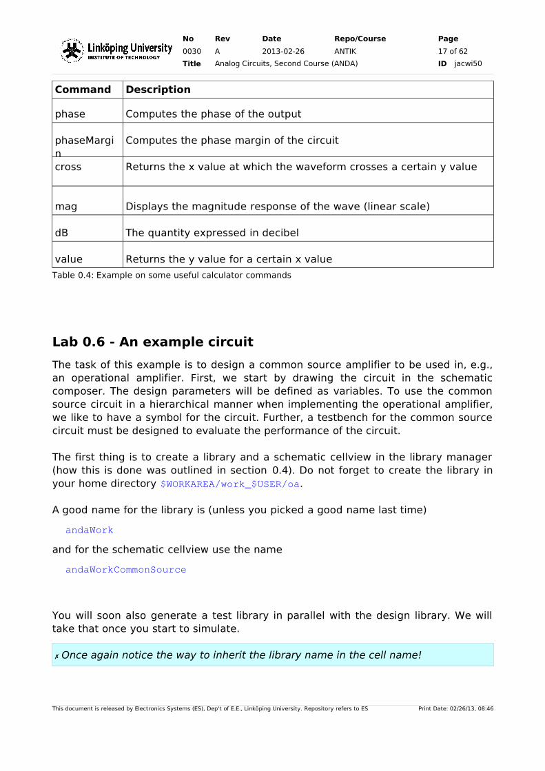
When you created the cellview an empty window will appear called Virtuoso Schematic Editing. In this window we will create the circuit shown in Figure 0.2.
Start by inserting the transistors by pressing the shortcut for insert instance 'i' and then choose the 1-V NMOS transistor from the library gpdk045, cell nmos1v, and view symbol which from now on will be written as gpdk045/nmos1v. You can directly add the transistor by using ctrl+shift+n.
The add instance window will now be updated and more fields will appear. In the Total Width field insert the variable inputWidth. In the Length field add the variable chLength. The NMOS transistor can now be placed in the schematic window.
✗ Once again - use clever names on the variables.
Continue with the PMOS transistors from gpdk045/pmos1v (ctrl+shift+p) and the current source from library analogLib/idc. Do not forget to add proper variable names to the Total Width and Length fields as for example has been done in Figure0.2. Use the same channel length variable for all transistors. You can mirror the objects by pressing the “Sideways” button in the add instance window. You can also copy objects by pressing the 'c'.
If you need to change the properties (or view in more detail) of the components in the schematic, click on the component and press 'q'.
Connect the components using wires. (The shortcut 'w' is handy). Do not forget to connect the bulks of each transistor to the correct supply voltage. The bulk is the fourth terminal, the one setting the body potential for the transistor. In an NMOS transistor it should normally be ground and for the PMOS it could, for example, be the supply.
Wires can be named by pressing the 'l' button. This sometimes simplifies the schematic as we now connect the wires by name instead. More importantly, it gives you access to intelligent names on the circuits nodes, rather than the default: net021, net013, etc. Add the names vpwr, vgnd, and vBias according to Figure 0.2.
Next step is to add pins. This is done by the shortcut 'p'. A new window will appear and you can add the pin names and then place them in the schematic. Use inputOutput pins for the supplies.
Your schematic should look like the one in Figure 0.2. The last step is to save the schematic by pressing shift + Y. If there are any errors, in the schematic, then a dialog box will appear and there will be some flashing markers on the schematic. An explanation to the errors will be shown in the CIW. Correct the errors and warnings and save the schematic. The schematic is now finalized.
This document is released by Electronics Systems (ES), Dep't of E.E., Linköping University. Repository refers to ES Print Date: 02/26/13, 08:46
No Rev Date Repo/Course Page
0030 A 2013-02-26 ANTIK 19 of 62
Title Analog Circuits, Second Course (ANDA) ID jacwi50
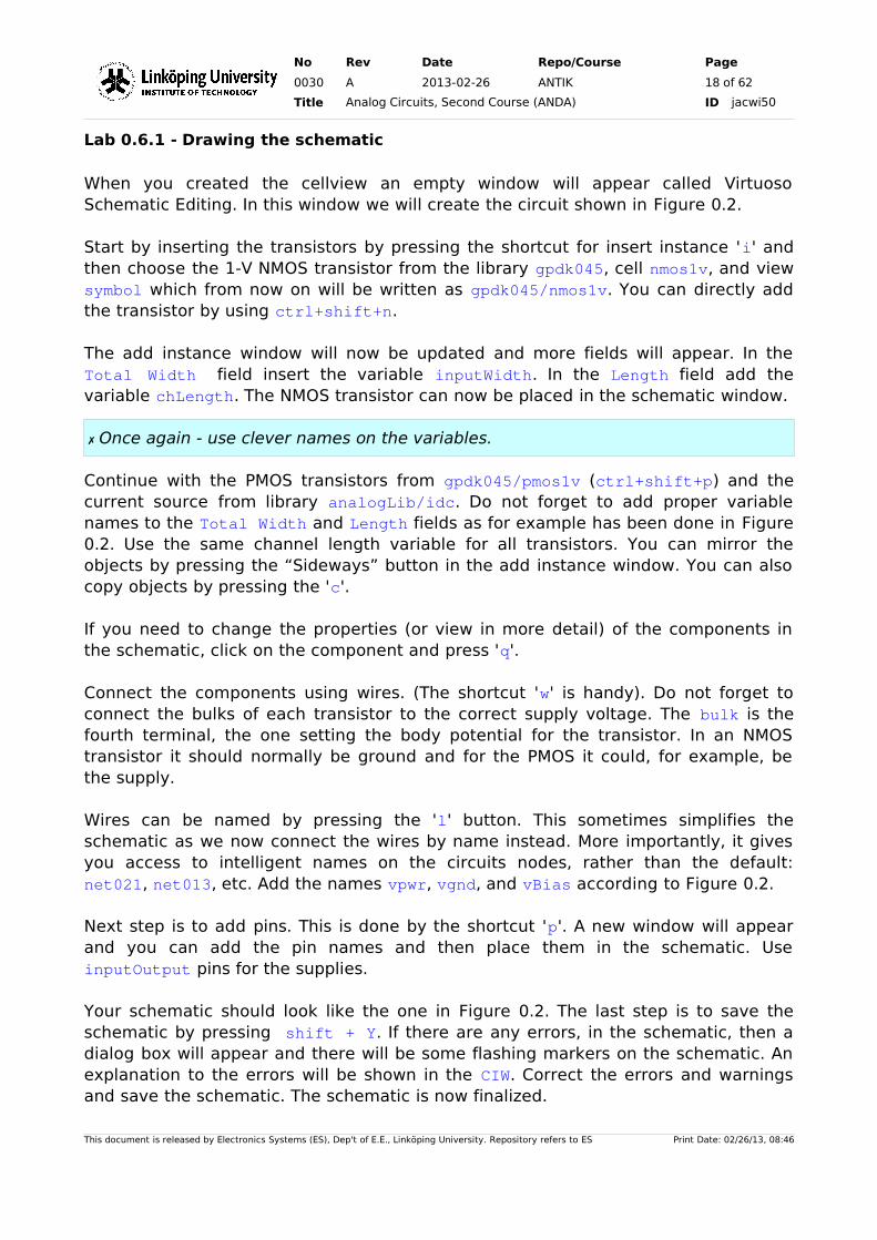
Lab 0.6.2 - Creating a symbol for the circuit
The next step is to create a symbol of the circuit so that it can be used several times at a higher level in the hierarchy. This can be done by the menu alternative
Create > Cellview > From Cellview
A dialog box will appear. Convince yourself that you are creating a symbol for the correct schematic, then press OK. A new dialog box named Symbol Generation Options will appear. Here you define where to place your pins on the symbol. Choose for example the positions as Table 0.5 suggests.
Left PinsvIn
Right PinsvOut
Top Pinsvpwr
Bottom Pinsvgnd
Table 0.5: Example of pin placements.
A symbol appears which consists of a green rectangle that will be visible when used in a schematic view, a red rectangle surrounding the green one which is the selection box of the circuit, and some solid red squares which are the input/output
This document is released by Electronics Systems (ES), Dep't of E.E., Linköping University. Repository refers to ES Print Date: 02/26/13, 08:46
No Rev Date Repo/Course Page
0030 A 2013-02-26 ANTIK 20 of 62
Title Analog Circuits, Second Course (ANDA) ID jacwi50
pins. In this view you can change the appearance of the symbol. For example, it can be changed to the one shown in Figure 0.3. A new shape can be drawn using the menu alternative
Create > Shape
When the symbol is ready and if you do not have the large red rectangle anymore (common mistake is to accidently remove it...) use the command:
Create > Selection Box
and then select to add it automatically. Notice that it is handy to make the selection box slightly smaller than the symbol, especially to have the pins outside the selection box. This makes it easier for the Cadence auto router on schematic level.
A couple of useful commands are alt + r and alt + a. The former generates new labels that are useful at higher levels in the hierarchy such that library name, cell name, etc., is displayed for easy browsing. The latter is used to place simulation annotation labels on the pins such that the simulator can annotate for example DC voltages, etc. With the command ctrl + 0 (on selected items) you can align the (selected) labels and pins to grid. The symbol must then be checked and saved by the menu alternative
File > Check and Save
or simply shift+x.
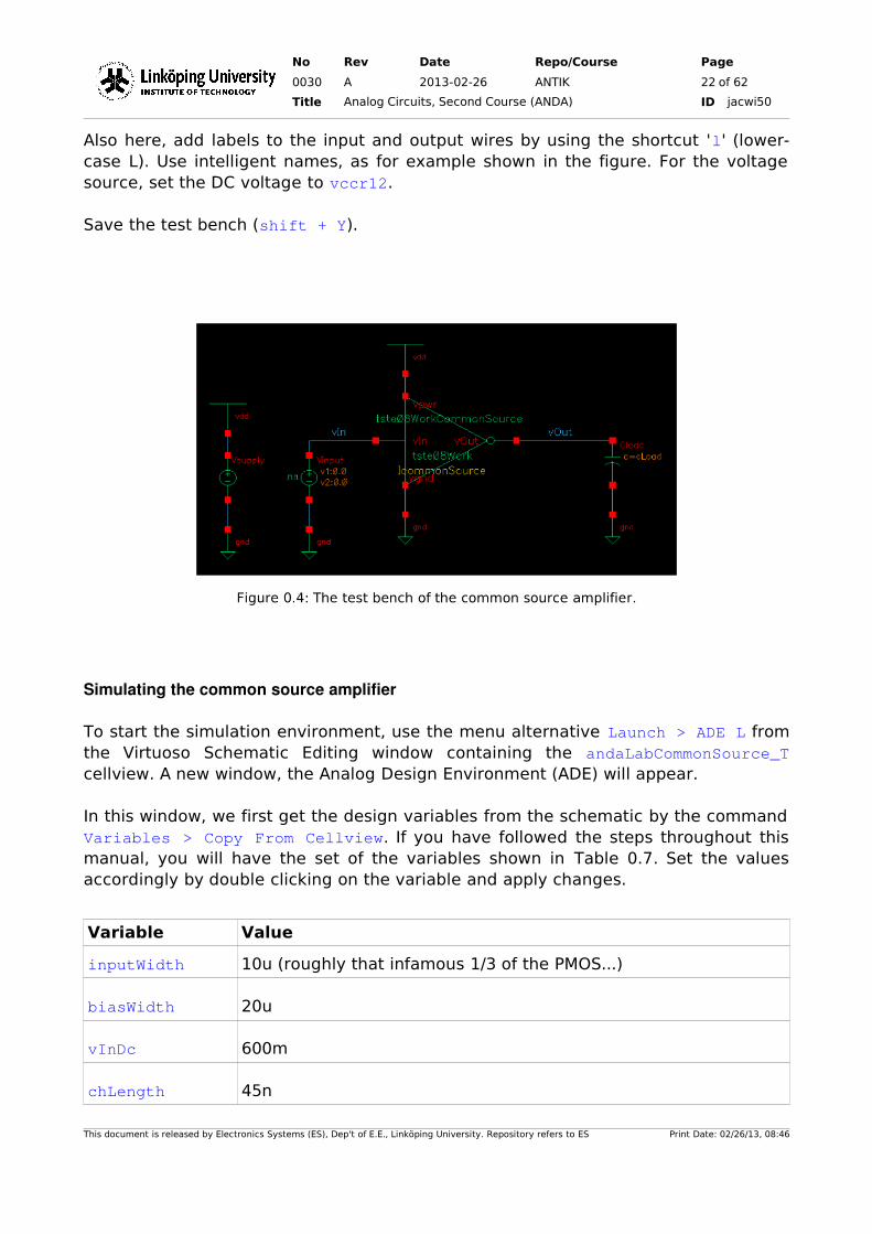
Lab 0.6.3 - Setting up the testbench
The last part is to setup the testbench of the common source circuit. The testbench should, in our case, be able to evaluate the small-signal gain from the input to the output, the slew rate of the circuit and the DC operation region of the transistors. This can be done by creating a new schematic cellview called
andaWorkCommonSource_T
in a new library for test benches:
This document is released by Electronics Systems (ES), Dep't of E.E., Linköping University. Repository refers to ES Print Date: 02/26/13, 08:46
No Rev Date Repo/Course Page
0030 A 2013-02-26 ANTIK 21 of 62
Title Analog Circuits, Second Course (ANDA) ID jacwi50
andaLabWorkTest
Use the same approach as you did previously to create the library: choose your work_$USER/oa/ area and attach to the gpdk045 technology file library. The testbench is shown in Error: Reference source not found.
✗ It is good practice to choose a separate library for your test files.
The left-most component is used to define the voltage between supply and ground. The parts for this structure are analogLib/vdd (ctrl+shift+s), analogLib/gnd (ctrl+shift+g) and analogLib/vdc (ctrl+shift+d). In the vdc symbol ,set the parameter DC voltage to 1.2 V which is used in this example. Leave the other fields in the vdc symbol empty.
A voltage source is connected at the input, it is found in analogLib/vpulse. Enter the parameters in Table 0.6 as component properties.
Parameter Value Explanation
AC magnitude
1 Using 1 V gives the transfer function at the output.
AC phase 0 The phase of the AC sinusoid
DC voltage vInDc The DC input voltage to the common source circuit.
Voltage 1 1.2 Start voltage for the pulse in the transient analysis.
Voltage 2 0 Second voltage for the pulse in the transient analysis.
Delay time 0.1n Delay from start of simulation.
Rise time 1p Rise time from voltage 1 to voltage 2.
Fall time 1p Fall time from voltage 2 to voltage 1.
Pulse width 10u The width of the pulse (time it will be 0 V)
Period 20u Time between repetition of the sequence.
Table 0.6: Parameters for the pulse source in the first test bench.
The common-source stage can be found in your library andaWork/andaWorkCommonSource and (probably) no parameters can be set to this component. At the output of the gain stage, we have the capacitor which is found in analogLib/cap (ctrl+shift+c) add the variable cLoad as the capacitance value.
This document is released by Electronics Systems (ES), Dep't of E.E., Linköping University. Repository refers to ES Print Date: 02/26/13, 08:46
No Rev Date Repo/Course Page
0030 A 2013-02-26 ANTIK 22 of 62
Title Analog Circuits, Second Course (ANDA) ID jacwi50
Also here, add labels to the input and output wires by using the shortcut 'l' (lower-case L). Use intelligent names, as for example shown in the figure. For the voltage source, set the DC voltage to vccr12.
Save the test bench (shift + Y).
Simulating the common source amplifier
To start the simulation environment, use the menu alternative Launch > ADE L from the Virtuoso Schematic Editing window containing the andaLabCommonSource_T cellview. A new window, the Analog Design Environment (ADE) will appear.
In this window, we first get the design variables from the schematic by the command Variables > Copy From Cellview. If you have followed the steps throughout this manual, you will have the set of the variables shown in Table 0.7. Set the values accordingly by double clicking on the variable and apply changes.
Variable Value
inputWidth 10u (roughly that infamous 1/3 of the PMOS...)
biasWidth 20u
vInDc 600m
chLength 45n
This document is released by Electronics Systems (ES), Dep't of E.E., Linköping University. Repository refers to ES Print Date: 02/26/13, 08:46
No Rev Date Repo/Course Page
0030 A 2013-02-26 ANTIK 23 of 62
Title Analog Circuits, Second Course (ANDA) ID jacwi50
Variable Value
iBias 100u
cLoad 10p
vccr12 1.2
Table 0.7: Design variables in the first test bench.
Continue to add the outputs that you like to see after you have simulated. This is done by the command Outputs > To Be Plotted > Select On Schematic. Select the output node and end the selection by pressing Escape. If you are selecting a wire the voltage of that wire will be displayed, the current can be displayed by selecting a node.
The last step is to choose the analysis types to be used by the menu alternative
Analyses > Choose...
In this case we would like to have a DC analysis. Check the dc analysis button in the appearing window and tick the Save DC Operating Point. In this case, we do not like to have any sweep so just click on the Apply button.
To compute the small-signal transfer function, an AC analysis must be performed. Check the ac analysis button and since we like to do a frequency sweep, just enter the start frequency for example 1 and the stop frequency at 500M. Then click Apply.
The last method is the transient analysis, so select the tran analysis and set the stop time to 30u.
The definition of the simulation is now complete. The simulation is started by clicking on the green traffic light. Possible errors will be shown in the CIW and in a spectre.out window. One common source of error is that you have not saved the schematic. Go back to the window and press shift+Y.
Most likely you have now bumped into the first issue. The widths of the transistors are too wide. The gpdk045 process puts a maximum limit on the transistor to W = 10 um. This is a common “problem” in design kits. Some kits behave differently and lets the tool handle this automatically. To solve this, you have to specify a number of fingers for the transistors. For each transistor add the following expression to the Fingers field:
ceil(iPar("w")/10u)
Now, the tool will calculate the number of fingers also for you and you can sweep the widths, etc., accordingly. Check and save and re-run. If more errors occur, talk to the lab assistant.
This document is released by Electronics Systems (ES), Dep't of E.E., Linköping University. Repository refers to ES Print Date: 02/26/13, 08:46
No Rev Date Repo/Course Page
0030 A 2013-02-26 ANTIK 24 of 62
Title Analog Circuits, Second Course (ANDA) ID jacwi50
Use the Results > Direct plot > Main form (or press '2' in the schematic window) to get the plot menu such that you can look at the different nodes for different analyses.
The performance parameters in Table 0.8 can be obtained with all transistors operating in the saturation (or subthreshold!) region with a little bit of tweaking. The performance measures can be found using the calculator but also by using the waveform window and cursors, etc. Go through the different menus and options in the waveform window to get yourself familiar with the tool.
Set for example the Y axis to logarithmic scale and find where the vOut curve crosses unity for the unity-gain frequency. Find out how you can set up expressions for DC gain, Unity-gain frequency etc using the Calculator. Take a look at the output set up for slew rate in andaLabTest/andaLabFirstSimulation_T/first_setup
Performance parameter Value
DC gain > 20 dB (11x)
Unity-gain frequency > 25 MHz
Slew rate on rising edge > 8 V/us
Table 0.8: Examples on simulated performance and some “typical” values for this process.
Enter the performance parameters that you obtained in Table 0.9
Performance parameter Value
DC gain
Unity-gain frequency
Slew rate on rising edge
Table 0.9: Performance parameters for CS amplifier
Double click on the cLoad variable in the ADE and change the value. Press Apply & Run Simulation each time you iterate. Fill in Table 0.10 too.
This document is released by Electronics Systems (ES), Dep't of E.E., Linköping University. Repository refers to ES Print Date: 02/26/13, 08:46
No Rev Date Repo/Course Page
0030 A 2013-02-26 ANTIK 25 of 62
Title Analog Circuits, Second Course (ANDA) ID jacwi50
What will happen with the bandwidth and the slew rate if the output capacitance, cLoad, is increased?.
Why is the falling-edge slew rate higher than the rising-edge slew rate?. Vary the bias current and comment on how the slew rate (falling,rising) change.
Table 0.10: Simulation observations.
Lab 0.6.4 - Some useful Daisy bind-keys
Table 0.11 compiles some useful Daisy bind-keys (non-standard Cadence keys).
Command Tool Explanation
F12 All Display list of Daisy bind-keys
ctrl+w All Kill window
ctrl+<no> Waveform Turning on/off subwindow <no> in waveform window
ctrl+f Waveform Increases the line width of waveform graphs
shift+Y Waveform Strips all the waveforms to separate graphs
shift+X Waveform Combines all waveforms into a single graph
alt+END All Open/raise library manager
alt+HOME All Raise CIW
alt+a Symbol Add simulation labels on symbol pins
ctrl+0 All Align to grid
This document is released by Electronics Systems (ES), Dep't of E.E., Linköping University. Repository refers to ES Print Date: 02/26/13, 08:46
No Rev Date Repo/Course Page
0030 A 2013-02-26 ANTIK 26 of 62
Title Analog Circuits, Second Course (ANDA) ID jacwi50
Command Tool Explanation
alt+r Symbol Add cell information labels on symbol
alt+shift+j Schematic Plot schematic to file
F5 Schematic+Sim Displays netlist in editable format
ctrlshift+key
Schematic Several different ways to quick-add analogLib components, d for vdd, v for voltage source, l for inductor, r for resistor, etc. See F12.
shift+c Schematic Add capacitor from analogLib
F7 Schematic Prints the hierarchy to file and text window
ctrl+3 Schematic+Sim Display operation region of selected transistors
Table 0.11: A list of some useful Daisy bind-keys
This document is released by Electronics Systems (ES), Dep't of E.E., Linköping University. Repository refers to ES Print Date: 02/26/13, 08:46
No Rev Date Repo/Course Page
0030 A 2013-02-26 ANTIK 27 of 62
Title Analog Circuits, Second Course (ANDA) ID jacwi50
-LAB1-
SINGLE-STAGE
AMPLIFIERS
Lab 1.1 - Introduction
This exercise is a quick recapture of your previous chapters. Transistors are generally characterized by a large number of parameters that the simulator uses. The generic process gives us however a limited number of parameters to access, like for example only the W and L of the transistor.
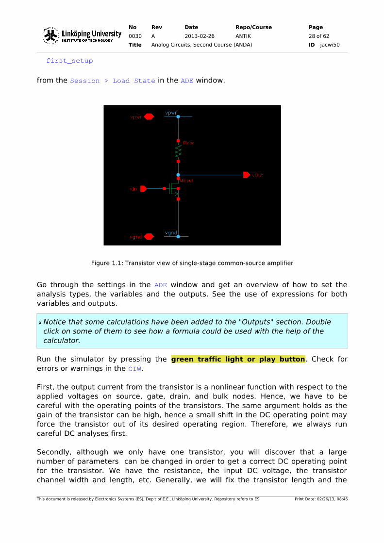
Consider the circuit in Figure 1.1. A resistor, Rload, is connected to the drain of the NMOS transistor, Minput. At the input we have to apply a voltage source. In the circuit, we have four nodes: input (vIn), output (vOut), ground (vgnd), and supply (vpwr).
Initiate the tools
Close all the schematics you have created so far. Open the cell view
andaLabTest / andaLabFirstSimulation_T
from the Library Manager which will contain an instantiation of the circuit in Figure1.1. Start the Analog Design Environment from the Launch menu. Load the state
This document is released by Electronics Systems (ES), Dep't of E.E., Linköping University. Repository refers to ES Print Date: 02/26/13, 08:46
No Rev Date Repo/Course Page
0030 A 2013-02-26 ANTIK 28 of 62
Title Analog Circuits, Second Course (ANDA) ID jacwi50
first_setup
from the Session > Load State in the ADE window.
Go through the settings in the ADE window and get an overview of how to set the analysis types, the variables and the outputs. See the use of expressions for both variables and outputs.
✗ Notice that some calculations have been added to the "Outputs" section. Double click on some of them to see how a formula could be used with the help of the calculator.
Run the simulator by pressing the green traffic light or play button. Check for errors or warnings in the CIW.
First, the output current from the transistor is a nonlinear function with respect to the applied voltages on source, gate, drain, and bulk nodes. Hence, we have to be careful with the operating points of the transistors. The same argument holds as the gain of the transistor can be high, hence a small shift in the DC operating point may force the transistor out of its desired operating region. Therefore, we always run careful DC analyses first.
Secondly, although we only have one transistor, you will discover that a large number of parameters can be changed in order to get a correct DC operating point for the transistor. We have the resistance, the input DC voltage, the transistor channel width and length, etc. Generally, we will fix the transistor length and the
This document is released by Electronics Systems (ES), Dep't of E.E., Linköping University. Repository refers to ES Print Date: 02/26/13, 08:46
No Rev Date Repo/Course Page
0030 A 2013-02-26 ANTIK 29 of 62
Title Analog Circuits, Second Course (ANDA) ID jacwi50
input and output voltages are given by a specification. Then, the transistor width is the first parameter that should be varied.
Thirdly, note that when you change a parameter, you do not only change the DC voltage, you also change other parameters, such as the gain of the circuit, bandwidth, etc. There is a delicate relation between a large number of factors. And more importantly there are a large number of trade-offs to be done.
Lab 1.1.1 - Run some simulations
The input DC voltage is 0.6 V. Which value on the transistor width, inputWidth, should you have in order to get 0.6 V at the output of the circuit as operating point?
✗ Hint: run a DC sweep on the transistor width, inputWidth. Check the waveform window for a likely candidate.
Transistor input width that gives you 0.6 V.
Go back to the ADE and change the design variable inputWidth to this new value. Re-run and check the AC analysis output now. Determine the DC gain and the -3-dB frequency!
DC gain -3-dB frequency
Table 1.1: Simulated DC gain and -3dB frequency with original DC level
Now, go back to the ADE and change the DC input voltage (variable vInDc) to 0.8 V. Rerun the simulation and find the DC gain and the -3dB frequency. Comments?
DC gain -3-dB frequency
Table 1.2: Simulated DC gain and -3dB frequency with new DC level
This document is released by Electronics Systems (ES), Dep't of E.E., Linköping University. Repository refers to ES Print Date: 02/26/13, 08:46
No Rev Date Repo/Course Page
0030 A 2013-02-26 ANTIK 30 of 62
Title Analog Circuits, Second Course (ANDA) ID jacwi50
This is what happens when you get in and out of “correct” DC operating regions, the gain is drastically changing (why?). Check the DC output voltage by using the menu Results > Annotate > DC Node Voltages.
Revert to a 0.5-V DC input level at the input (reset vInDc). What is the output resistance, and DC output voltage? (Hint: use the command Results > Print > DC Node Voltage and Results > Print > DC Operation Point.)
What is the total power consumption? It is found using the menu Results > Print > DC Operation Point followed by clicking on the power supply voltage source, vSupply.
Is the transistor operating in its saturation region? Check that V DSV DS , sat and V GSV T using the command Results> Print > DC Operation Point followed by clicking on the transistor. (There is even a region parameter that you can look at, but it is somewhat cryptically encoded as 0, 1, 2, 3, 4). You can also select the transistor and press ctrl+3.
Operation region
Check if the simulated gain is reasonably well aligning with your derived g m/ gout ratio.
This document is released by Electronics Systems (ES), Dep't of E.E., Linköping University. Repository refers to ES Print Date: 02/26/13, 08:46
No Rev Date Repo/Course Page
0030 A 2013-02-26 ANTIK 31 of 62
Title Analog Circuits, Second Course (ANDA) ID jacwi50
Comments?
Lab 1.1.2 - Analog simulation techniques
To avoid simulation problems, such as convergence issues, long simulation times, etc., we mostly try not to use too ideal components. Therefore, it is convenient to define the signal sources to have an output impedance of say 50 Ohms and 100 fF. In the same way, we have to add a load impedance to the test circuit. Mostly, we deal with CMOS circuits and transistor gates form the input of preceding stages. This implies that the load resistance is infinite (ideally), but the load capacitance can be something in the order of say 25 fF.
Go back to the testbench and see the daisyRcLink block on the left-hand side. Select it and press 'q' for properties. It has two parameters: Capacitance and Resistance that can be filled in by the user. Step inside the block and look at the connections by selecting the block and use 'e'. (Select schematic as view name, normally default). Notice that it is bidirectional (the resistance is split in half on both “sides” of the capactior).
✗ Try to use this block with reasonable values throughout your simulations.
In analog design, we rarely use minimum channel length, Lmin , for gain transistors. Eventhough it would maximize the W /L ratio, a minimum channel length is not guaranteeing a proper L , it is often too poorly modelled in the simulator since it is “defined” by the digital circuits. and often the mismatch increases. Instead, one normally uses a minimum channel length of approximately 1.5 Lmin to 4 Lmin . In this lab series we use 45 to 90 nm for the generic process. However, shorter channel lengths can be used in order to increase some performance metrics but with a lower circuit yield.
Lab 1.2 - CMOS gain stages
In amplifier design on a printed circuit board (PCB), resistive load is often used. The disadvantage with using a resistive load is that the gain cannot be very high, since the resistance must be large. This will cause the current to be small in order to keep the voltage levels at descent values. Therefore, active loads are preferred. This will significantly increase the gain and hence the DC levels are very important. Adjustments in the order of mV will completely change the transfer function of the gain stage.
This document is released by Electronics Systems (ES), Dep't of E.E., Linköping University. Repository refers to ES Print Date: 02/26/13, 08:46
No Rev Date Repo/Course Page
0030 A 2013-02-26 ANTIK 32 of 62
Title Analog Circuits, Second Course (ANDA) ID jacwi50
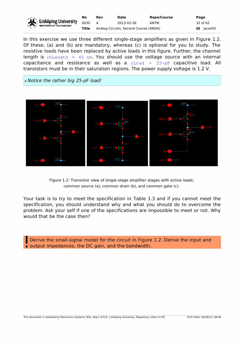
In this exercise we use three different single-stage amplifiers as given in Figure 1.2. Of these, (a) and (b) are mandatory, whereas (c) is optional for you to study. The resistive loads have been replaced by active loads in this figure. Further, the channel length is chLength = 45 nm. You should use the voltage source with an internal capacitance and resistance as well as a cLoad = 25pF capacitive load. All transistors must be in their saturation regions. The power supply voltage is 1.2 V.
✗ Notice the rather big 25-pF load!
Your task is to try to meet the specification in Table 1.3 and if you cannot meet the specification, you should understand why and what you should do to overcome the problem. Ask your self if one of the specifications are impossible to meet or not. Why would that be the case then?
Derive the small-signal model for the circuit in Figure 1.2. Derive the input and output impedances, the DC gain, and the bandwidth. !
This document is released by Electronics Systems (ES), Dep't of E.E., Linköping University. Repository refers to ES Print Date: 02/26/13, 08:46

No Rev Date Repo/Course Page
0030 A 2013-02-26 ANTIK 33 of 62
Title Analog Circuits, Second Course (ANDA) ID jacwi50
Common source
Common drain
Common gate (opt.)
Unit
Bias DC voltage(s)0.5 0.55 0.6 (PMOS),
0.8 (NMOS)V
Input DC voltage0.6 1.0 0.2 V
Output DC voltage0.6 0.45 0.6 V
DC gain35 3 16 dB
Table 1.3: Specification on single-stage active buffer/amplifiers.
Lab 1.2.1 - DC and AC simulations
Copy the schematic andaLabCommonSource_T from the andaLabTest library to your local andaWorkTest so that you get write access. Now, you should simulate this building block and also notice that you have an additional bias voltage source for the added transistor in the active case. Also notice that the common-source stage with resistive load is also pasted into the schematic test bench. You will therefore simulate two amplifiers simultaneously.
Use sweeps for the DC simulation to find transistor sizes. Be very careful! You may have to increase the accuracy, i.e., more points in the sweep, to find proper values.
Use AC simulation to find the DC gain, bandwidth, unity gain frequency and phase margin. You can find the results by using the Calculator from the Waveform window, and by looking at the waveforms accessible from the Results >Direct Plot menu.
When finding the proper signal swings at input and output we sweep the input DC level from 0 to 1.2 V. The input- and output ranges are defined as the voltage ranges for which all the transistors are saturated.
You can find these results by doing a Parametric Analysis from the Tools menu, and then find the transistor operating regions by using Results > Print > DC Operating Points after you have selected the transistors. The region is 0 for cut-off, 1 for linear, and 2 for saturated. For the sweeps, you can use the calculator to plot the OP("region") of the transistors. Select the ranges in which all transistors belong to region 2 (saturated).
✗ Ask the lab assistant to help you out if needed.
You will need to do several sweeps with increased accuracy around the switching points.
This document is released by Electronics Systems (ES), Dep't of E.E., Linköping University. Repository refers to ES Print Date: 02/26/13, 08:46
No Rev Date Repo/Course Page
0030 A 2013-02-26 ANTIK 34 of 62
Title Analog Circuits, Second Course (ANDA) ID jacwi50
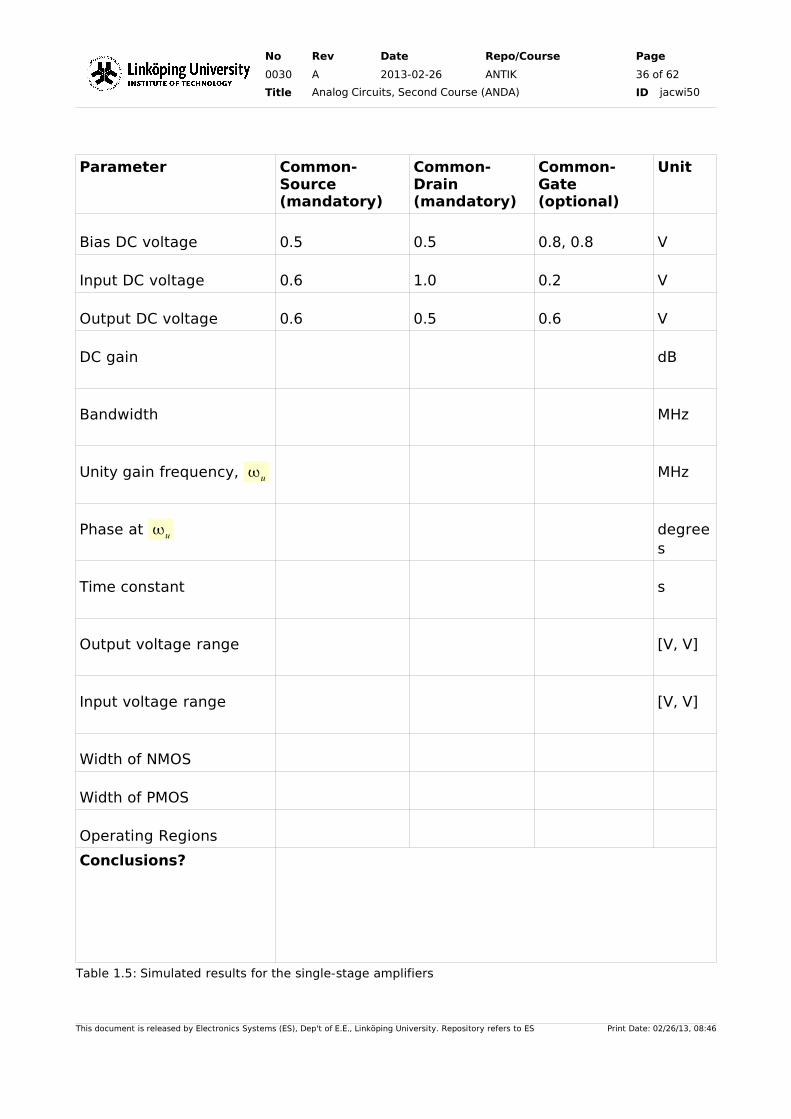
You will also find the andaLabCommonGate_T and andaLabCommonDrain_T from the andaLabTest library. Run these testbenches too and fill in the simulated results in Table 1.5. Save all states so that you can reuse your findings later on, choose clever names.
Lab 1.3 - Transient simulation
We will also investigate the settling time of the circuits as well as the general time-domain behavior. By using the analogLib/vpulse source we can apply a voltage step at the input. Select the input source and press 'q' for properties and verify that the values from Table 1.4 are used in the vpulse fields.
Field Value
Voltage 1 vInDc
Voltage 2 vInDc + 0.001
Delay time 1u
Rise time 10n
Fall time 10n
Pulse width 8u
Period 10uTable 1.4: vpulse values
Start by letting simulation run up to 10 us by adding a transient analysis (tran) in the ADE (Analyses > Setup ...).
✗ Depending on what transistor sizes you use, you may need to increase/decrease the pulse width and simulation time.
Note that for the optional low-gain stages (b and c in Figure 1.2) you may have to change the +0.001 to a somewhat larger value, like 0.01 to 0.1, in order to see good output results. Run and plot the input and output signals. Measure the time constant. When a small step is applied to the input of a circuit with a dominating pole, the output signal will have the form
V (t )=V (0)+ΔV⋅(1−e−t / τ ) (1.1)
This document is released by Electronics Systems (ES), Dep't of E.E., Linköping University. Repository refers to ES Print Date: 02/26/13, 08:46
No Rev Date Repo/Course Page
0030 A 2013-02-26 ANTIK 35 of 62
Title Analog Circuits, Second Course (ANDA) ID jacwi50
where V is a function of the DC gain of the circuit times the size of the step at the input. In other words, the final output voltage is V 0 V . The time constant is defined as
V =V 0 V 1−e−1≈V 00.63 V (1.2)
Compare the time constant with the output pole of your system as
=1p1≈C L⋅Rout (1.3)
Comments? What will happen if you have a too large step? What other effects might influence your measured results.
✗ Hint: Look at the waveform and check if it is a linear curve or an exponentially increasing/decreasing.
Fill in the simulated time constant(s) in Table 1.5 and then wrap up by saving all cellviews and simulation states. You save the simulation states from the File > Save State menu in the ADE. This will help you to retrieve your simulator settings next time you log on.
✗ Pick an intelligent name for your state, and avoid the default spectre_state1. Choose something like: acSimulationSetup or so
This document is released by Electronics Systems (ES), Dep't of E.E., Linköping University. Repository refers to ES Print Date: 02/26/13, 08:46
No Rev Date Repo/Course Page
0030 A 2013-02-26 ANTIK 36 of 62
Title Analog Circuits, Second Course (ANDA) ID jacwi50
Parameter Common-Source (mandatory)
Common-Drain (mandatory)
Common-Gate (optional)
Unit
Bias DC voltage 0.5 0.5 0.8, 0.8 V
Input DC voltage 0.6 1.0 0.2 V
Output DC voltage 0.6 0.5 0.6 V
DC gain dB
Bandwidth MHz
Unity gain frequency, u MHz
Phase at u degrees
Time constant s
Output voltage range [V, V]
Input voltage range [V, V]
Width of NMOS
Width of PMOS
Operating Regions
Conclusions?
Table 1.5: Simulated results for the single-stage amplifiers
This document is released by Electronics Systems (ES), Dep't of E.E., Linköping University. Repository refers to ES Print Date: 02/26/13, 08:46
No Rev Date Repo/Course Page
0030 A 2013-02-26 ANTIK 37 of 62
Title Analog Circuits, Second Course (ANDA) ID jacwi50
-LAB2-
TRANSMISSION
LINES AND
TERMINATION
Lab 2.1 - Introduction
In this lab, the task is to consider the electrical communication between a "transmitter" and a "receiver" and also taking supply and ground planes into account. To be able to model this, we are going to study transmission lines and different ways to terminate a wire/line. We will simulate the circuits in the Cadence Virtuoso environment.
What we will try to learn today is how the transmission line acts like a carrier of waves throughout your circuit. In short, due to the "vast" distances on a PCB combined with high-speed signals and accurate clock edges, we cannot ignore the physical distances and properties of the wire. In "traditional" electrical circuits, this is quite commonly the case. For example, look at an RC-circuit, we model a voltage source, a resistor, and a capacitive load. In reality, the voltage source will have a non-zero output impedance and the interconnect wires will be associated with parasitic resistance, capacitance, and inductance.
This document is released by Electronics Systems (ES), Dep't of E.E., Linköping University. Repository refers to ES Print Date: 02/26/13, 08:46
No Rev Date Repo/Course Page
0030 A 2013-02-26 ANTIK 38 of 62
Title Analog Circuits, Second Course (ANDA) ID jacwi50
To understand this, we will mainly study the transient behavior in detail. For example, what happens if you apply a square-wave pulse to a transmission line? This could be a clock signal, or data, that should be transported from one chip to another. What will it look like?
✗ One trick is to zoom in on the rising and falling edges of the pulses. The effects will be more clearly visible there. Also, if you increase the signal frequency (reduce the time period of the pulses) you will see even more dramatic effects if your system is not well-balanced.
Lab 2.2 - Preparations
You might have to copy some of the cells to your own working directories in order to be able to change them. (Some of the cells are controlled by parameters and thus do not necessarily have to be copied.)
For this lab, you will find the cells to be simulated/modified in the following Cadence library
andaLab2
Browse through the different cells and try to get an idea of what to do in this lab before you get too carried away.
Lab 2.3 - Transmission lines and termination
For theory behind transmission lines, etc., see the course book, attend the lecture, and use any other valid information you can find on the topic. A short description of the theory will be given in this section.
Lab 2.3.1 - Transmission line theory
Often one refers to a 50-Ohm or 75-Ohm transmission lines or similar types of grading. Here it could be worth mentioning that it is an impedance level and mainly being reactive rather than resistive.
Typically, when defining the transmission line we consider the wave equations (or the two telegrapher's equations):
d2V (x)
d x2=−(R+ jωL)⋅
d I (x)d x
and d I ( x)d x
=−(G+ jωC )⋅V ( x ) , (2.1)
where R is the sheet resistance per transmission line length (dx) , G is the conductance between the line and the shield (per length unit), L and C are the inductance and capacitance, respectively, per unit length. V (x) and I (x ) are the
This document is released by Electronics Systems (ES), Dep't of E.E., Linköping University. Repository refers to ES Print Date: 02/26/13, 08:46
No Rev Date Repo/Course Page
0030 A 2013-02-26 ANTIK 39 of 62
Title Analog Circuits, Second Course (ANDA) ID jacwi50
voltage and current at a given position x along the transmission line. Now, combining the two telegrapher's equations yields something like
d2V (x)
d x2=γ
2⋅V (x) (2.2)
where γ2 is defined as
γ2=(R+ jω L)⋅(G+ j ωC ) (2.3)
The general solution to this second-order ODE is given by
V (x )=V 0p⋅e−γ x
+V 0n⋅eγ x and I ( x)= I0p⋅e
−γ x+ I 0n⋅e
γ x (2.4)
where all constants are (could be) complex numbers, dependent on material, etc. In the equations we can read out two types of components effectively describing two waves going in two different directions. In some sense we have four different variables to keep track of.
One can realize that the values V 0p ,V 0n , I 0p , I 0n can be determined by considering e.g. the start and/or end of the transmission line. We can plug in e.g. x=0 (at the transmitter or generator) and see that:
V (0)=V 0p+V 0n and I (0)=I 0p+ I 0n . (2.5)
From this we can conclude:
✗ The boundary conditions determine the behavior of the waves travelling through the transmission line! This is why source and load termination is so important! More on this later.
The characteristic impedance of a transmission line can be found by observing how much the voltage changes if the current changes along the line, and we see that this is a constant (independent on the wire length!):
Z 0=√ R+ jω LG+ jωC (which could be a complex number) (2.6)
If the transmission line is lossless (often assumed for short wire, short tracks on the PCB) the R≈0 . It is also very likely to assume that the conductance between shield and wire/track is very, very small, we get to:
This document is released by Electronics Systems (ES), Dep't of E.E., Linköping University. Repository refers to ES Print Date: 02/26/13, 08:46
No Rev Date Repo/Course Page
0030 A 2013-02-26 ANTIK 40 of 62
Title Analog Circuits, Second Course (ANDA) ID jacwi50
Z 0≈√ LC (which is a real number) (2.7)
The L and C can be calculated by finding the permeabilities between the wire and shield, as well as the inductivity along the wire.
✗ Once again, do not consider the characteristic impedance as a 50-Ohm resistive "load" along the wire.
With the concept of waves in mind, it is (hopefully) a bit easier to understand that a voltage, or an edge of a voltage can "travel" along the wire. However, what happens when the traveling wave reaches one of the end points? Will it just die and vanish into limbo? No, not really. The situtation depends on the boundary conditions as mentioned before. Dependet on how the line is terminated (in both load and generator) the wave will behave differently. For some conditions it might get absorbed, for some it may reflect with full power, and for some it may reflect with full power - but with opposite phase, etc. Anything in between could happen too. To understand this mechanism, we can study the reflection coefficient, ρ (or Γ ):
ρ=Γ=ZT−Z0ZT+Z 0
(2.8)
where Z T could be the termination resistance in either end of the wire dependent on which port we want to study. The rest of the story is "simple" (if we for time being ignore the fact that both Z T and Z 0 could be complex numbers...):
✗ If a voltage wave has an amplitude of V pk , a wave with an amplitude of ρ⋅V pk will be reflected.
A complex refelection coefficient, ρ , would give a phase shift too. From (2.8), and still assuming real-valued Z T , Z 0>0 we see that −1≤ρ<1 . We can identify three "extreme" values:
• Z T=0 , i.e., short-circuit. In this case the reflection coefficient is ρ=−1 and the wave will be reflected with full magnitude and negative amplitude.
• Z T=∞ , i.e., open-circuit. In this case the reflection coefficient is ρ=+1 and the wave will be reflected with full magnitude and positive amplitude.
• Z T=Z0 , i.e., "perfect" termination. In this case the reflection coefficient is ρ=0 and the wave will be fully absorbed in the termination load and hence no reflection.
This document is released by Electronics Systems (ES), Dep't of E.E., Linköping University. Repository refers to ES Print Date: 02/26/13, 08:46
No Rev Date Repo/Course Page
0030 A 2013-02-26 ANTIK 41 of 62
Title Analog Circuits, Second Course (ANDA) ID jacwi50
Dependent on the reflection coefficient (well, the termination) a wave can now build up and even be cancelled (!) at different positions along the wire. It could also be that a wave travels a long a wire and gets reflected and builds up critical voltage levels that could actually (in the long term) damage circuits along the wire.
In most cases it is now up to the board designer (well, the tools in some sense) to find the characteristic impedance and dimension them properly. However, often we have a lot of special cases. for example wires tapping off in different directions (effectively creating different characteristic impedances for different segments of the wire), several CMOS drivers/chips hooking up to the clock wire on different physical positions, etc. How should we terminate them properly in order to minimize the influence of rogue traveling waves along the wire.
Lab 2.4 - Impedance matching
Your first exercise will be to observe the effects of reflections along a transmission wire. In the theory section above, we have already highlighted what the design target should be. However, in order to relate our formulas to the reality (well, the simulator in our case, so close to reality), we need to get some hands-on experience.
In Figure 0.1 a snapshot of the circuit to be tested is shown. You find it in
andaLab2 > andaLabTestTline_T
in your potentially copied library. Otherwise copy it from andaLab2.
So, consider the test bench in Figure 0.1, it contains a transmitter, a generator, implemented by a port in Cadence. The port is associated with an output impedance and the load, the sink, has a certain termination resistor/resistance, Rterm/rLoad.
In short, in the examples below, you should explain the waveforms' behavior, such as for example the width of the "stairs" and the height of each step.
✗ Remember to zoom in!
You have a couple of saved simulation states associated with this testbench (try them out first to test the circuit and familiarize yourself with it). The generator sends away a square wave pulse towards the load.
This document is released by Electronics Systems (ES), Dep't of E.E., Linköping University. Repository refers to ES Print Date: 02/26/13, 08:46

No Rev Date Repo/Course Page
0030 A 2013-02-26 ANTIK 42 of 62
Title Analog Circuits, Second Course (ANDA) ID jacwi50
Check the waveforms at the input and output. What do they look like?
What happens if you increase the signal frequency? What if the frequency is a very high value?
Now, you should vary the load resistance (rLoad) from a low value to a high value and observe the simulated waveforms. This can be done using the parametric analysis tool.
Tools > parametric analysis
Sweep the load resistance (let the variable rLoad vary from e.g. 1 to 200 Ohms) in say 50 steps.
This document is released by Electronics Systems (ES), Dep't of E.E., Linköping University. Repository refers to ES Print Date: 02/26/13, 08:46
No Rev Date Repo/Course Page
0030 A 2013-02-26 ANTIK 43 of 62
Title Analog Circuits, Second Course (ANDA) ID jacwi50
What do you see on the pulse trains when changing the load resistance?
To speed up the lab a bit, the simulation tool has been prepared such that it has a cost function for the power dissipated in the load.
For which value on rLoad do you get highest power dissipated in the load?
Vary the length (it is a parameter, lStrip) of the transmission line preferrably through a parametric sweep rather than manually pressing the Run button.
Sweep the length from 0.001 to 0.2 (i.e., 1 mm to 20 cm).
✗ If you do many sweeps (also rLoad), then put the lStrip variable on top for better plotting (use the blue up/down arrows in the parametric analysis' tool).
How do the waveforms depend on the length of the transmission line?
Given that you are changing the length of the transmission line - what can you conclude about the power delivered to the load?
✗ Do not necessarily trust the predefined formula reporting the power!
This document is released by Electronics Systems (ES), Dep't of E.E., Linköping University. Repository refers to ES Print Date: 02/26/13, 08:46
No Rev Date Repo/Course Page
0030 A 2013-02-26 ANTIK 44 of 62
Title Analog Circuits, Second Course (ANDA) ID jacwi50
Lab 2.4.1 - Conclusions
Please also answer the questions below to eventually wrap up this part of the lab.
Which mathematical expression(s) help(s) us to select the load termination?
Which impedance value on the transmission line is "optimum"?
Which value on the source resistance, rPort, is "optimum"?
This document is released by Electronics Systems (ES), Dep't of E.E., Linköping University. Repository refers to ES Print Date: 02/26/13, 08:46
No Rev Date Repo/Course Page
0030 A 2013-02-26 ANTIK 45 of 62
Title Analog Circuits, Second Course (ANDA) ID jacwi50
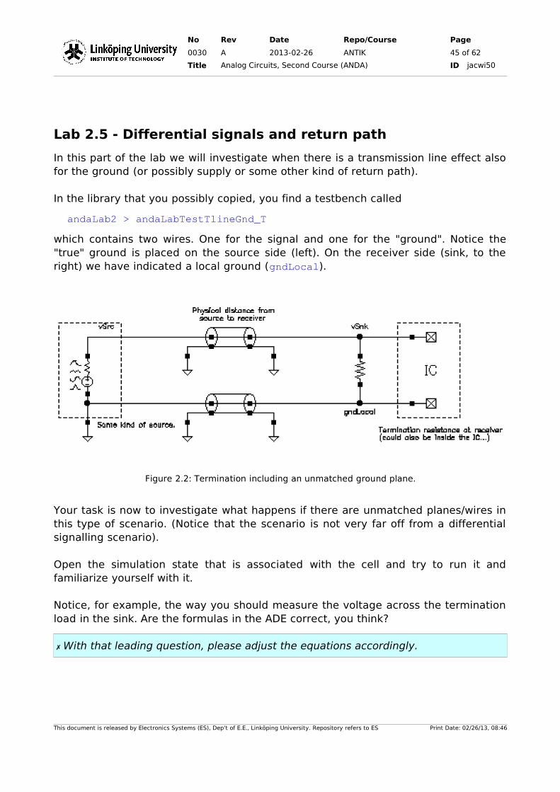
Lab 2.5 - Differential signals and return path
In this part of the lab we will investigate when there is a transmission line effect also for the ground (or possibly supply or some other kind of return path).
In the library that you possibly copied, you find a testbench called
andaLab2 > andaLabTestTlineGnd_T
which contains two wires. One for the signal and one for the "ground". Notice the "true" ground is placed on the source side (left). On the receiver side (sink, to the right) we have indicated a local ground (gndLocal).
Your task is now to investigate what happens if there are unmatched planes/wires in this type of scenario. (Notice that the scenario is not very far off from a differential signalling scenario).
Open the simulation state that is associated with the cell and try to run it and familiarize yourself with it.
Notice, for example, the way you should measure the voltage across the termination load in the sink. Are the formulas in the ADE correct, you think?
✗ With that leading question, please adjust the equations accordingly.
This document is released by Electronics Systems (ES), Dep't of E.E., Linköping University. Repository refers to ES Print Date: 02/26/13, 08:46

No Rev Date Repo/Course Page
0030 A 2013-02-26 ANTIK 46 of 62
Title Analog Circuits, Second Course (ANDA) ID jacwi50
Plot the waveforms at both the sink and source (generator). Conclusions?
Now, start to do some sweeps over the different termination and transmission line lengths and characteristic impedances.
Supported by some mathematical observations as well as practical conclusions from the previous part of the lab, you should know in what direction to go to "stabilize" the system.
✗ You might have to do modifications to the schematic!
Can you make the waveforms behave "properly"?
If so, how should you solve the problem with a second wire and its characteristic impedance?
Given the scenario in Figure 2.2, make a picture/sketch of how the waves in such a system would travel back and forth through the transmission lines.
This document is released by Electronics Systems (ES), Dep't of E.E., Linköping University. Repository refers to ES Print Date: 02/26/13, 08:46
No Rev Date Repo/Course Page
0030 A 2013-02-26 ANTIK 47 of 62
Title Analog Circuits, Second Course (ANDA) ID jacwi50
Sketch the traveling waves scenario
This document is released by Electronics Systems (ES), Dep't of E.E., Linköping University. Repository refers to ES Print Date: 02/26/13, 08:46

No Rev Date Repo/Course Page
0030 A 2013-02-26 ANTIK 48 of 62
Title Analog Circuits, Second Course (ANDA) ID jacwi50
Lab 2.6 - Splitted wires
In the previous part of this lab, we did in fact do a rather dirty model of the ground plane just to see how two transmission lines would "cooperate" (or not). Dependent on the settings you used in your simulations it illustrates quite well the complexities when matching several paths.
A scenario a bit similar to this is shown in Figure 2.3 where we have splitted the wire. The generator intends to drive two sources. This could be a clock that should time two different circuits.
The task is now to investigate how we can match up the system without changing the characteristic impedances on the transmission lines!
In this case, you would definitely have to change the schematic and thus have to copy it to your own working area. The original is found in
andaLab2 > andaLabTestTlineFork_T
As we can see from Figure 2.3 (and in the cell view) we have three different transmission lines and dependent on the impedance levels there could be traveling waves from essentially any point to any other point. A wave can be reflected from sink 1 and travel to sink 2, etc.
First, start the simulation state associated with the cell. Run some simulations and familiarize yourself with the testbench and the variables that are available.
This document is released by Electronics Systems (ES), Dep't of E.E., Linköping University. Repository refers to ES Print Date: 02/26/13, 08:46
No Rev Date Repo/Course Page
0030 A 2013-02-26 ANTIK 49 of 62
Title Analog Circuits, Second Course (ANDA) ID jacwi50
Given the previous lab, it might not come as a surprise that you have to add some series resistors in order to match the transmission lines against each other. The task is however to find out how this should be done properly and "align" the system.
In fact, we will give you quite loose instructions this time: simply come back with a properly designed interconnection network.
Describe your network here:
✗ If you have the odt of this file, why not do a snapshot of the testbench and paste in the table above.
This document is released by Electronics Systems (ES), Dep't of E.E., Linköping University. Repository refers to ES Print Date: 02/26/13, 08:46
No Rev Date Repo/Course Page
0030 A 2013-02-26 ANTIK 50 of 62
Title Analog Circuits, Second Course (ANDA) ID jacwi50
-LAB3-
DECOUPLING
CAPACITORS AND
SUPPLY FILTERS
Lab 3.1 - Introduction
As one might expect, there are many sources of disturbances on a PCB board or on a chip. As we saw in the previous lab, it could be due to unmatched terminals where waves could travel back and forth and result in undersired behavior. There could be other disturbances traveling through many different paths.
Disturbances could also travel along the supply and ground wires. There could, for example, be a source somewhere injecting noise at a certain frequency (or frequency band) and then this noise can then be transported to a sink which also happens to be sensitive to disturbances at the frequency range in question. We need to find ways to keep these disturbances under control.
In short, this can be done in two different ways:
• design your internal circuitry such that it is insensitive to supply fluctuations (for example, fully differential circuits are a starting point for this). On-chip filters that filter out e.g. high-frequency noise.
This document is released by Electronics Systems (ES), Dep't of E.E., Linköping University. Repository refers to ES Print Date: 02/26/13, 08:46
No Rev Date Repo/Course Page
0030 A 2013-02-26 ANTIK 51 of 62
Title Analog Circuits, Second Course (ANDA) ID jacwi50
• design your board such that the noise is cancelled by adding off-chip filters. This can be done such that any high-frequency component that travels along the supply line will then be effectively cancelled between positive supply and ground.
Both options obviously have many more flavours to them. It is however not within the scope of this laboratory to explore all possible options. Equally true is that, since we are not operating in an ideal world, both of these approaches also have limited success and not all disturbances can be cancelled out. Theoretically perhaps, but not practically.
So, in this lab, we focus on the second approach, i.e., on the way to add a supply filter to the PCB design such that high-frequency components are filtered out. This we will do with decoupling capacitors. The basic idea with decoupling capacitors is to effectively short two wires at high frequencies, thus suppressing the noise. Let us see some of the theory first, though.
Lab 3.2 - Decoupling capacitors
If we would connect a capacitor between a wire and ground, there would be an impedance of
Z=1sC
(3.1)
between the two nodes. At low frequencies (s=0) this value is very high. At DC, the impedance is infinite, Z=∞ . At high frequencies, there is a short, as Z=0 for s→∞ .
At high frequencies, any disturbances would effectively be shorted and "directly" returned through the ground wire. The disturbance would not reach inside the chip if the decoupling capacitors are placed close to the chip.
Dependent on the application, we could say that a good decoupling requires that the impedance (or reactance) is less than 1 Ohm for a certain region in the frequency domain.
Let us look at the expression above:
∣Z∣=1
∣s∣C=1⇒∣s∣=
1C⇒∣ f ∣=
12πC
(3.2)
For frequencies higher than 1/2πC the impedance is less than 1 Ohm. So, if we need to cancel frequencies (to the extent 1 Ohm permits...) above 1 MHz, we would need a decoupling capacitance of approximately 130 nF. For 1 kHz, we would need a capacitance of 130 uF. (This is a quite large value, and as is examplified by the
This document is released by Electronics Systems (ES), Dep't of E.E., Linköping University. Repository refers to ES Print Date: 02/26/13, 08:46
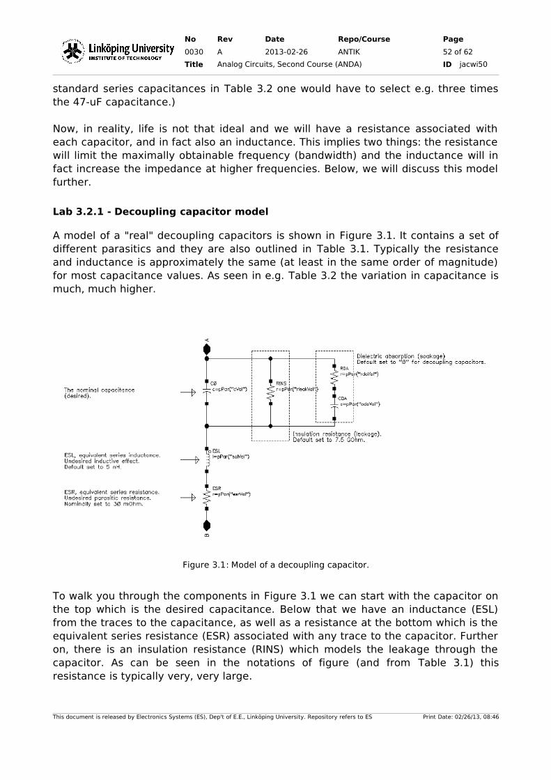
No Rev Date Repo/Course Page
0030 A 2013-02-26 ANTIK 52 of 62
Title Analog Circuits, Second Course (ANDA) ID jacwi50
standard series capacitances in Table 3.2 one would have to select e.g. three times the 47-uF capacitance.)
Now, in reality, life is not that ideal and we will have a resistance associated with each capacitor, and in fact also an inductance. This implies two things: the resistance will limit the maximally obtainable frequency (bandwidth) and the inductance will in fact increase the impedance at higher frequencies. Below, we will discuss this model further.
Lab 3.2.1 - Decoupling capacitor model
A model of a "real" decoupling capacitors is shown in Figure 3.1. It contains a set of different parasitics and they are also outlined in Table 3.1. Typically the resistance and inductance is approximately the same (at least in the same order of magnitude) for most capacitance values. As seen in e.g. Table 3.2 the variation in capacitance is much, much higher.
To walk you through the components in Figure 3.1 we can start with the capacitor on the top which is the desired capacitance. Below that we have an inductance (ESL) from the traces to the capacitance, as well as a resistance at the bottom which is the equivalent series resistance (ESR) associated with any trace to the capacitor. Further on, there is an insulation resistance (RINS) which models the leakage through the capacitor. As can be seen in the notations of figure (and from Table 3.1) this resistance is typically very, very large.
This document is released by Electronics Systems (ES), Dep't of E.E., Linköping University. Repository refers to ES Print Date: 02/26/13, 08:46
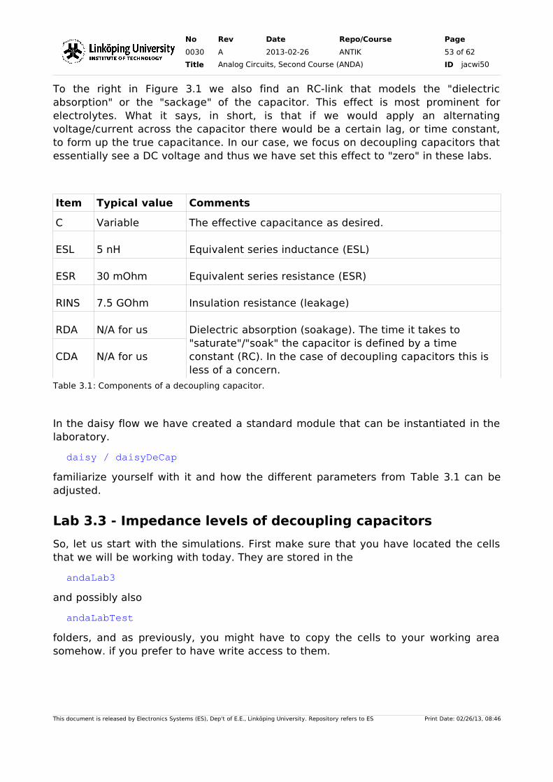
No Rev Date Repo/Course Page
0030 A 2013-02-26 ANTIK 53 of 62
Title Analog Circuits, Second Course (ANDA) ID jacwi50
To the right in Figure 3.1 we also find an RC-link that models the "dielectric absorption" or the "sackage" of the capacitor. This effect is most prominent for electrolytes. What it says, in short, is that if we would apply an alternating voltage/current across the capacitor there would be a certain lag, or time constant, to form up the true capacitance. In our case, we focus on decoupling capacitors that essentially see a DC voltage and thus we have set this effect to "zero" in these labs.
Item Typical value Comments
C Variable The effective capacitance as desired.
ESL 5 nH Equivalent series inductance (ESL)
ESR 30 mOhm Equivalent series resistance (ESR)
RINS 7.5 GOhm Insulation resistance (leakage)
RDA N/A for us Dielectric absorption (soakage). The time it takes to "saturate"/"soak" the capacitor is defined by a time constant (RC). In the case of decoupling capacitors this is less of a concern.
CDA N/A for us
Table 3.1: Components of a decoupling capacitor.
In the daisy flow we have created a standard module that can be instantiated in the laboratory.
daisy / daisyDeCap
familiarize yourself with it and how the different parameters from Table 3.1 can be adjusted.
Lab 3.3 - Impedance levels of decoupling capacitors
So, let us start with the simulations. First make sure that you have located the cells that we will be working with today. They are stored in the
andaLab3
and possibly also
andaLabTest
folders, and as previously, you might have to copy the cells to your working area somehow. if you prefer to have write access to them.
This document is released by Electronics Systems (ES), Dep't of E.E., Linköping University. Repository refers to ES Print Date: 02/26/13, 08:46
No Rev Date Repo/Course Page
0030 A 2013-02-26 ANTIK 54 of 62
Title Analog Circuits, Second Course (ANDA) ID jacwi50
Lab 3.3.1 - Impedance characteristics
Find the
andaLabTestDeCap_T
cell and launch the ExampleSetup state for your simulator.
Now plot the impedance characteristics. The tool has been prepared to give you the impedance of the 22-nF and 100-nF capacitors as well as the combined decoupling capacitance.
Locate the three waveforms in your plot window. Which one is which, etc.? Notice that you might have to change the Y axis to a logarithmic scale to get a better picture. Also go to the ADE window and see how the formulas are created:
abs((1 / (IF("/Vprobe_22/PLUS") / VF("/vCap"))))
you might need to create your own functions shortly.
What is this formula expressing? Impedance? Admittance? Reactance?
What happens at approximately 160 MHz? Explain!
Now change the two values capacitor values., let them be 2.2 uF and 22 uF.
This document is released by Electronics Systems (ES), Dep't of E.E., Linköping University. Repository refers to ES Print Date: 02/26/13, 08:46
No Rev Date Repo/Course Page
0030 A 2013-02-26 ANTIK 55 of 62
Title Analog Circuits, Second Course (ANDA) ID jacwi50
What happens with the waveforms compared to prior example? Explain!
Consider the graphs that you just got - where (at which frequency) is the notch, i.e., minimum value, of the combined curve? Find an approximate analytical expression for this point given the model of your capacitance.
We could continue to simulate and investigate the behavior for different capacitances like this, but could be tedious. We need to be a bit more systematic.
Define the safe area as the frequency range in which the impedance level is less than 1 Ohm, i.e., ∣Z∣<1 . You can now "fool the tool" a bit by constructing a new expression given the total impedance like:
(1 abs(Z_cap_tot1)/(Z_cap_tot1) )/2.0
which will give you a kind of digital waveform. Open the calculator and paste the expression in the entry form and press the plot. For frequencies where the waveform is '1' your decoupling is in the "safe region".
For the single decoupling transistors, what is (are) the safe range(s)?
This document is released by Electronics Systems (ES), Dep't of E.E., Linköping University. Repository refers to ES Print Date: 02/26/13, 08:46
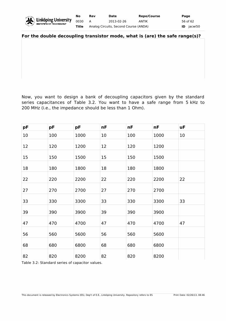
No Rev Date Repo/Course Page
0030 A 2013-02-26 ANTIK 56 of 62
Title Analog Circuits, Second Course (ANDA) ID jacwi50
For the double decoupling transistor mode, what is (are) the safe range(s)?
Now, you want to design a bank of decoupling capacitors given by the standard series capacitances of Table 3.2. You want to have a safe range from 5 kHz to 200 MHz (i.e., the impedance should be less than 1 Ohm).
pF pF pF nF nF nF uF
10 100 1000 10 100 1000 10
12 120 1200 12 120 1200
15 150 1500 15 150 1500
18 180 1800 18 180 1800
22 220 2200 22 220 2200 22
27 270 2700 27 270 2700
33 330 3300 33 330 3300 33
39 390 3900 39 390 3900
47 470 4700 47 470 4700 47
56 560 5600 56 560 5600
68 680 6800 68 680 6800
82 820 8200 82 820 8200
Table 3.2: Standard series of capacitor values.
This document is released by Electronics Systems (ES), Dep't of E.E., Linköping University. Repository refers to ES Print Date: 02/26/13, 08:46
No Rev Date Repo/Course Page
0030 A 2013-02-26 ANTIK 57 of 62
Title Analog Circuits, Second Course (ANDA) ID jacwi50
Select a minimum number of capacitors that fulfills this target.
Given your results, can you formulate a rule-of-thumb for selecting decoupling capacitors?
This document is released by Electronics Systems (ES), Dep't of E.E., Linköping University. Repository refers to ES Print Date: 02/26/13, 08:46
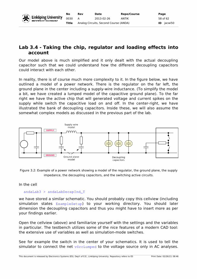
No Rev Date Repo/Course Page
0030 A 2013-02-26 ANTIK 58 of 62
Title Analog Circuits, Second Course (ANDA) ID jacwi50
Lab 3.4 - Taking the chip, regulator and loading effects into account
Our model above is much simplified and it only dealt with the actual decoupling capacitor such that we could understand how the different decoupling capacitors could interact with each other.
In reality, there is of course much more complexity to it. In the figure below, we have outlined a model of a power network. There is the regulator on the far left, the ground plane in the center including a supply-wire inductance. (To simplify the model a bit, we have created a lumped model of the capacitive ground plane). To the far right we have the active chip that will generated voltage and current spikes on the supply while switch the capacitive load on and off. In the center-right, we have illustrated the bank of decoupling capacitors. Inside these, we will also assume the somewhat complex models as discussed in the previous part of the lab.
In the cell
andaLab3 > andaLabDecapInd_T
we have stored a similar schematic. You should probably copy this cellview (including simulation states ExampleSetup) to your working directory. You should later dimension the decoupling capacitors and thus you might have to insert more as per your findings earlier.
Open the cellview (above) and familiarize yourself with the settings and the variables in particular. The testbench utilizes some of the nice features of a modern CAD tool: the extensive use of variables as well as simulation-mode switches.
See for example the switch in the center of your schematics. It is used to tell the simulator to connect the net vSrcLumped to the voltage source only in AC analyses.
This document is released by Electronics Systems (ES), Dep't of E.E., Linköping University. Repository refers to ES Print Date: 02/26/13, 08:46
No Rev Date Repo/Course Page
0030 A 2013-02-26 ANTIK 59 of 62
Title Analog Circuits, Second Course (ANDA) ID jacwi50
In a similar way, the switch to the right (just below "On-chip driver") makes sure that the chip is only connected to the supply network in transient simulation mode.
The other indicated advantage, was the extensive use of variables. See in the "Design Variables" list how we have also added:
WITH_INDUCTOR, WITH_GROUNDPLANE, WITH_DECOUPLING, WITH_REGULATOR
These are supposed to be set as digital variables, i.e., 0 or 1. Then they are used in other variable definitions for which we have added the scaling value. See for example the cVal100 (for one of the decoupling capacitors) where the default 1f is multiplied by WITH_DECOUPLING. The other WITH_'s are hopefully rather self-explanatory.
✗ The nice thing now is that you can run parametric sweeps for different WITH settings! In fact, all four of them at the same time, giving you 16 results up-front.
We have also helped you out a bit and created a function for determining the supply impedance.
So, first some checks that you have understood the basics of the testbench:
What's the capacitance of the ground plane between supply and ground?
What's the value of the supply inductance?
How many periods are run in transient simulation?
What's the rise and fall time of the switched signal?
This document is released by Electronics Systems (ES), Dep't of E.E., Linköping University. Repository refers to ES Print Date: 02/26/13, 08:46
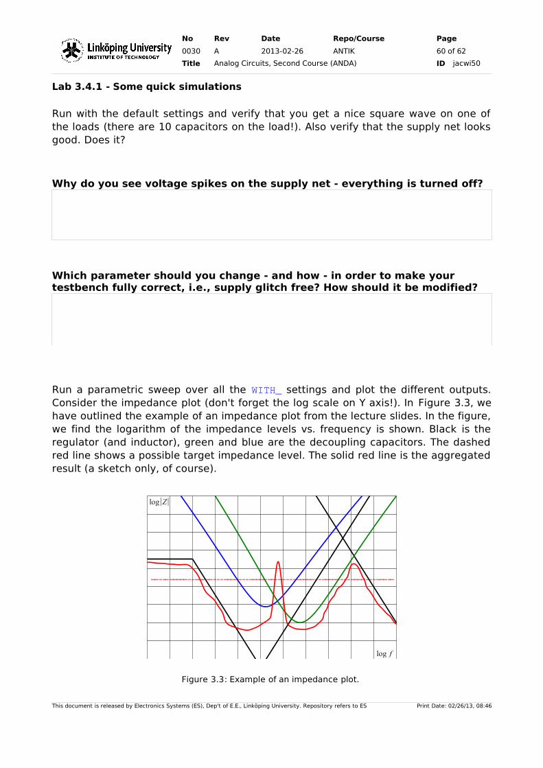
No Rev Date Repo/Course Page
0030 A 2013-02-26 ANTIK 60 of 62
Title Analog Circuits, Second Course (ANDA) ID jacwi50
Lab 3.4.1 - Some quick simulations
Run with the default settings and verify that you get a nice square wave on one of the loads (there are 10 capacitors on the load!). Also verify that the supply net looks good. Does it?
Why do you see voltage spikes on the supply net - everything is turned off?
Which parameter should you change - and how - in order to make your testbench fully correct, i.e., supply glitch free? How should it be modified?
Run a parametric sweep over all the WITH_ settings and plot the different outputs. Consider the impedance plot (don't forget the log scale on Y axis!). In Figure 3.3, we have outlined the example of an impedance plot from the lecture slides. In the figure, we find the logarithm of the impedance levels vs. frequency is shown. Black is the regulator (and inductor), green and blue are the decoupling capacitors. The dashed red line shows a possible target impedance level. The solid red line is the aggregated result (a sketch only, of course).
This document is released by Electronics Systems (ES), Dep't of E.E., Linköping University. Repository refers to ES Print Date: 02/26/13, 08:46
Figure 3.3: Example of an impedance plot.
log f
log∣Z∣
No Rev Date Repo/Course Page
0030 A 2013-02-26 ANTIK 61 of 62
Title Analog Circuits, Second Course (ANDA) ID jacwi50
Present your screen shots below. Do you see any peaks? Why?
If you change the signal frequency - do you see any differences?
Lab 3.4.2 - Dimensioning task
So, the task now is quite simple: design the decoupling capacitor bank to get your impedance level below 2 Ohm for all (!) frequencies. Once again use the standard capacitors from the table in the previous section to meet the requirements.
Remember that you might have to change the schematics too.
Do not only look at the frequency domain, also consider the transient.
This document is released by Electronics Systems (ES), Dep't of E.E., Linköping University. Repository refers to ES Print Date: 02/26/13, 08:46

No Rev Date Repo/Course Page
0030 A 2013-02-26 ANTIK 62 of 62
Title Analog Circuits, Second Course (ANDA) ID jacwi50
What capacitors and capacitance values did you use?
Does the pulsed output waveform (transient) look good now?
This document is released by Electronics Systems (ES), Dep't of E.E., Linköping University. Repository refers to ES Print Date: 02/26/13, 08:46