analog and low-power design lecture 20 (c) 20031 lecture 20 current source biasing and mos amplifier...
TRANSCRIPT

Analog and Low-Power Design LeAnalog and Low-Power Design Lecture 20 (c) 2003cture 20 (c) 2003
11
Lecture 20Lecture 20Current Source Biasing and MOS Current Source Biasing and MOS
Amplifier DesignAmplifier Design
Michael L. BushnellMichael L. BushnellCAIP Center and WINLABCAIP Center and WINLAB
ECE Dept., Rutgers U., Piscataway, NJECE Dept., Rutgers U., Piscataway, NJ
• Temperature and supply-independent biasingTemperature and supply-independent biasing• OPAMP designOPAMP design• SummarySummary

Analog and Low-Power Design LeAnalog and Low-Power Design Lecture 20 (c) 2003cture 20 (c) 2003
22
Temperature and Supply-Temperature and Supply-Independent BiasingIndependent Biasing
• Biasing must also be independent of process variationsBiasing must also be independent of process variations– Critical for MOS circuitsCritical for MOS circuits
• Bias Bias I I fluctuations with fluctuations with TT, , VVDDDD, and process cause , and process cause wasted energywasted energy
• Supply-independent biasing is importantSupply-independent biasing is important– Avoid injecting high-Avoid injecting high-ff noise on power lines into circuit noise on power lines into circuit
signal pathsignal path

Analog and Low-Power Design LeAnalog and Low-Power Design Lecture 20 (c) 2003cture 20 (c) 2003
33
Supply-Independent BiasingSupply-Independent Biasing
• Refer bias circuit to potential other thanRefer bias circuit to potential other than V VDDDD:: VVt t – threshold voltage of MOSFET– threshold voltage of MOSFET
VVbg bg – band-gap voltage– band-gap voltage
VVtt of dissimilar devices of dissimilar devices
VVBEBE of parasitic bipolar transistor in CMOS of parasitic bipolar transistor in CMOS
VVTT – thermal voltage (k T / q) – thermal voltage (k T / q)
Zener diode breakdown V – too high breakdown VZener diode breakdown V – too high breakdown V
• Self-biasing requires a start-up circuitSelf-biasing requires a start-up circuit– Must force circuit into equilibrium in desired stable stateMust force circuit into equilibrium in desired stable state

Analog and Low-Power Design LeAnalog and Low-Power Design Lecture 20 (c) 2003cture 20 (c) 2003
44
VVtt Referenced Self-Biased Circuit Referenced Self-Biased Circuit
• Fig 12.25a (old book)Fig 12.25a (old book)
Analog and Low-Power Design LeAnalog and Low-Power Design Lecture 20 (c) 2003cture 20 (c) 2003
55
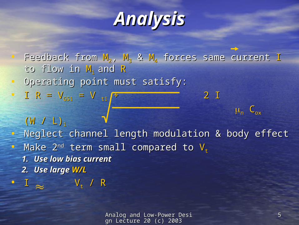
AnalysisAnalysis
• Feedback from Feedback from MM22, , MM33 & & MM44 forces same current forces same current II to flow in to flow in MM11
and and RR• Operating point must satisfy:Operating point must satisfy:• I R = VI R = VGS1GS1 = V = V t1t1 + 2 I + 2 I nn C Coxox (W / L) (W / L)11
• Neglect channel length modulation & body effectNeglect channel length modulation & body effect• Make 2Make 2ndnd term small compared to term small compared to VVtt
1.1. Use low bias currentUse low bias current2.2. Use large Use large W/LW/L
• I VI Vtt / R / R

Analog and Low-Power Design LeAnalog and Low-Power Design Lecture 20 (c) 2003cture 20 (c) 2003
66
Analysis (continued)Analysis (continued)
• If 2If 2ndnd term included, O/P current is slightly reduced but term included, O/P current is slightly reduced but TT and and VVDDDD dependence is the same dependence is the same
• Must ensure stability – need to verify that feedback loop gain is Must ensure stability – need to verify that feedback loop gain is < 1 at operating point< 1 at operating point– Do by breaking the loop, injecting a signal, & checking the gainDo by breaking the loop, injecting a signal, & checking the gain
• Must determine degree of supply independenceMust determine degree of supply independence– Channel length modulation in Channel length modulation in MM22 & & MM11 causes bias current causes bias current
variationvariation• Reduce variation with cascode current sourceReduce variation with cascode current source
Analog and Low-Power Design LeAnalog and Low-Power Design Lecture 20 (c) 2003cture 20 (c) 2003
77
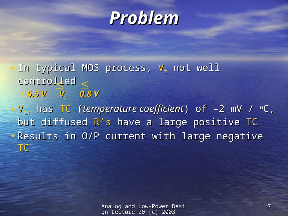
ProblemProblem
• In typical MOS process,In typical MOS process, V Vtt not well controlled not well controlled 0.5 V V0.5 V Vtt 0.8 V 0.8 V
• VVtntn has has TCTC ( (temperature coefficienttemperature coefficient) of –2 mV / ) of –2 mV / ooC, but C, but diffused diffused R’sR’s have a large positive have a large positive TCTC
• Results in O/P current with large negativeResults in O/P current with large negative TC TC

Analog and Low-Power Design LeAnalog and Low-Power Design Lecture 20 (c) 2003cture 20 (c) 2003
88
Delta VDelta Vtt Temperature Temperature
IndependenceIndependence
• Use differences in Use differences in VVtt of two devices of same polarity of two devices of same polarity but with different channel implantsbut with different channel implants
• Advantage: Advantage: TC’sTC’s of two devices cancel to first order of two devices cancel to first order– Can get O/P Voltage Can get O/P Voltage TCTC as low as 20 ppm / as low as 20 ppm / ooCC

Analog and Low-Power Design LeAnalog and Low-Power Design Lecture 20 (c) 2003cture 20 (c) 2003
99
VVTT Referenced Biasing Referenced Biasing
• Fig 12.25b (old book)Fig 12.25b (old book)

Analog and Low-Power Design LeAnalog and Low-Power Design Lecture 20 (c) 2003cture 20 (c) 2003
1010
DisadvantagesDisadvantages
• Large initial tolerance in O/P voltage valueLarge initial tolerance in O/P voltage value– Threshold voltages have large toleranceThreshold voltages have large tolerance
• Extensively used for precision voltage references in Extensively used for precision voltage references in nnMOS and CMOSMOS and CMOS– Need to trim a resistor to adjust absolute O/P voltageNeed to trim a resistor to adjust absolute O/P voltage

Analog and Low-Power Design LeAnalog and Low-Power Design Lecture 20 (c) 2003cture 20 (c) 2003
1111
VVBEBE Referenced Biasing Referenced Biasing
• Fig 12.26 (old book)Fig 12.26 (old book)

Analog and Low-Power Design LeAnalog and Low-Power Design Lecture 20 (c) 2003cture 20 (c) 2003
1212
AnalysisAnalysis• pnppnp is a parasitic bipolar device in is a parasitic bipolar device in pp-substrate CMOS-substrate CMOS• Can also use a parasitic Can also use a parasitic npnnpn transistor transistor• Feedback involving Feedback involving MM11, , MM22, , MM33, , MM44 forces emitter current in forces emitter current in QQ11 to match R to match R
currentcurrent I R = VI R = VTT ln I or I = V ln I or I = VBE1BE1
IISS R R• Advantage: Advantage: VVBEBE is well-controlled, with 5% variation is well-controlled, with 5% variation• Disadvantage: Disadvantage: VVBEBE has a negative has a negative TCTC of –2 mV / of –2 mV / ooCC
– RR has a strong positive has a strong positive TCTC– Leads to a strong negative Leads to a strong negative TCTC in bias current in bias current– Can reduce reference current variation with a cascode or Wilson current Can reduce reference current variation with a cascode or Wilson current
sourcesource

Analog and Low-Power Design LeAnalog and Low-Power Design Lecture 20 (c) 2003cture 20 (c) 2003
1313
VVTT-Referenced Biasing (Thermal -Referenced Biasing (Thermal
Voltage)Voltage)• Fig 12.27 (old book)Fig 12.27 (old book)
Analog and Low-Power Design LeAnalog and Low-Power Design Lecture 20 (c) 2003cture 20 (c) 2003
1414
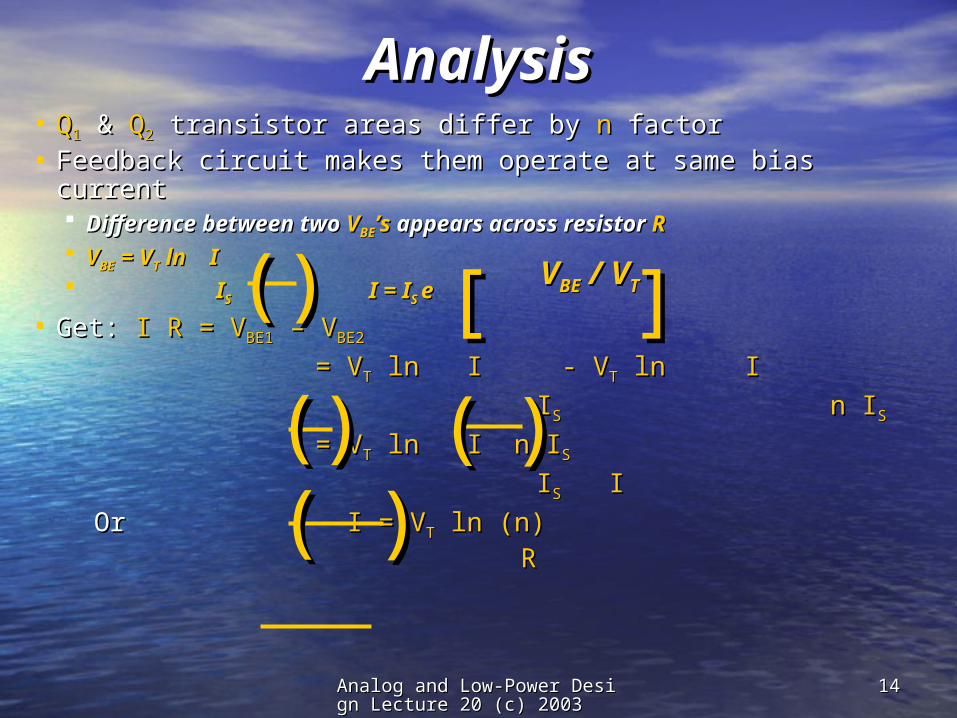
AnalysisAnalysis• QQ11 & & QQ22 transistor areas differ by transistor areas differ by nn factor factor• Feedback circuit makes them operate at same bias currentFeedback circuit makes them operate at same bias current
Difference between two Difference between two VVBEBE’s’s appears across resistor appears across resistor RR VVBEBE = V = VTT ln I ln I IIS S I = II = IS S ee
• Get: Get: I R = VI R = VBE1BE1 – V – VBE2BE2
= V= VTT ln I - V ln I - VTT ln I ln I IISS n I n ISS
= V= VTT ln I n I ln I n ISS
IISS I I Or Or I = VI = VTT ln (n) ln (n) RR
VVBEBE / V / VTT)) (( ]] [[
)) (( )) (()) ((

Analog and Low-Power Design LeAnalog and Low-Power Design Lecture 20 (c) 2003cture 20 (c) 2003
1515
DiscussionDiscussion
• Advantage: Advantage: VVT T has positive temperature coefficient has positive temperature coefficient (V(VTT = kT / q) = kT / q)
• RR has a positive has a positive TCTC, so current output is relatively , so current output is relatively TT independentindependent
Analog and Low-Power Design LeAnalog and Low-Power Design Lecture 20 (c) 2003cture 20 (c) 2003
1616
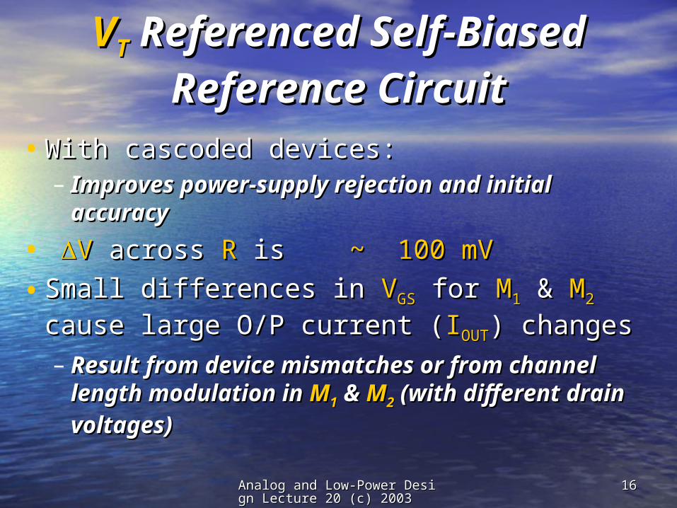
VVTT Referenced Self-Biased Referenced Self-Biased
Reference CircuitReference Circuit• With cascoded devices:With cascoded devices:
– Improves power-supply rejection and initial accuracyImproves power-supply rejection and initial accuracy
• VV across across RR is is ~ 100 mV~ 100 mV• Small differences in Small differences in VVGSGS for for MM11 & & MM22 cause large O/P cause large O/P
current (current (IIOUTOUT) changes) changes– Result from device mismatches or from channel length Result from device mismatches or from channel length
modulation in modulation in MM11 & & MM22 (with different drain voltages) (with different drain voltages)

Analog and Low-Power Design LeAnalog and Low-Power Design Lecture 20 (c) 2003cture 20 (c) 2003
1717
Self-Biased Reference CircuitSelf-Biased Reference Circuit
• Fig 12.28 (old book)Fig 12.28 (old book)

Analog and Low-Power Design LeAnalog and Low-Power Design Lecture 20 (c) 2003cture 20 (c) 2003
1818
Band-Gap Referenced BiasingBand-Gap Referenced Biasing
• Fig 12.29 (old book)Fig 12.29 (old book)

Analog and Low-Power Design LeAnalog and Low-Power Design Lecture 20 (c) 2003cture 20 (c) 2003
1919
AnalysisAnalysis• IIM8M8 draindrain = V = VTT ln (n) ln (n) RR• VV00 = V = VBEBE + V + VTT ln (n) x R ln (n) x R RR = V= VBEBE + x V + x VTT ln (n) ln (n)• OPAMP maintains OPAMP maintains VV00 at both + and – terminals due to feedback at both + and – terminals due to feedback IIOUTOUT = V = V00 / R / R22
• Advantage: By weighting Advantage: By weighting VVBEBE and and VVTT components, one gets a components, one gets a voltage of any desired voltage of any desired TCTC– Can exactly cancel an Can exactly cancel an R TCR TC
)) ((

Analog and Low-Power Design LeAnalog and Low-Power Design Lecture 20 (c) 2003cture 20 (c) 2003
2020
WeightingWeighting
• Parameter Parameter xx determines weighting of determines weighting of VVTT-dependent -dependent portion:portion:
1.1. Can use only common collector transistorsCan use only common collector transistors
2.2. OPAMP has MOS transistors, so their input offset OPAMP has MOS transistors, so their input offset voltage and input offset voltage temperature drift voltage and input offset voltage temperature drift influence O/P voltage of the referenceinfluence O/P voltage of the reference
• Must remove offset with analog storage and cancellationMust remove offset with analog storage and cancellation

Analog and Low-Power Design LeAnalog and Low-Power Design Lecture 20 (c) 2003cture 20 (c) 2003
2121
SummarySummary
• Temperature and supply-independent Temperature and supply-independent biasingbiasing
• OPAMP designOPAMP design