an10800 using the blf578 in the 88 mhz to 108 mhz fm band · generation of high voltage ldmos ......
TRANSCRIPT
AN10800Using the BLF578 in the 88 MHz to 108 MHz FM bandRev. 01 — 13 October 2009 Application note
Document information
Info Content
Keywords BLF578, performance, high-efficiency tuning set-up, high voltage LDMOS,amplifier implementation, Class-C CW, FM band, pulsed power
Abstract This application note describes the design and the performance of theBLF578 for Class-C CW and FM type applications in the 88 MHz to108 MHz frequency range. The major aim has been to illustrate tuningset-up performance which targets very high-efficiency operation atreduced output power
NXP Semiconductors AN10800Using the BLF578 in the 88 MHz to 108 MHz FM band
Revision history
Rev Date Description
01 20091013 Initial version
AN10800_1 © NXP B.V. 2009. All rights reserved.
Application note Rev. 01 — 13 October 2009 2 of 23
Contact informationFor more information, please visit: http://www .nxp.com
For sales office addresses, please send an email to: salesad [email protected]
NXP Semiconductors AN10800Using the BLF578 in the 88 MHz to 108 MHz FM band
1. Introduction
The BLF578 is a new, 50 V, push-pull transistor using NXP Semiconductors’ 6th
generation of high voltage LDMOS technology. The two push-pull sections of the deviceare completely independent of each other inside the package. The gates of the device areinternally protected by the integrated ElectroStatic Discharge (ESD) diode.
The device is unmatched and is designed for use in applications below 600 MHz wherevery high power and efficiency are required. Typical applications are FM/VHF broadcast,laser or Industrial Scientific and Medical (ISM) applications.
Great care has been taken during the design of the high voltage process to ensure thatthe device achieves high ruggedness. This is a critical parameter for successful broadcastoperations. The device can withstand greater than a 10:1 VSWR for all phase angles atfull operating power.
Another design goal was to minimize the size of the application circuit. This is important inthat it allows amplifier designers to maximize the power in a given amplifier size. Thedesign highlighted in this application note achieves over 1 kW in the 88 MHz to 108 MHzband in a space smaller than 50.8 mm × 101.6 mm (2 ” × 4 ”). The circuit only needs to beas wide as the transistor itself, enabling transistor mounting in the final amplifier to be asclose as physically possible while still providing adequate room for the circuitimplementation.
This application note describes the design and the performance of the BLF578 forClass-C CW and FM type applications in the 88 MHz to 108 MHz frequency band. It mustbe noted that the device is very powerful and more than 1200 W of pulsed power hasbeen generated at 225 MHz. This application note describes tuning set-up performancewhich targets very high-efficiency operation at somewhat reduced output powers.
AN10800_1 © NXP B.V. 2009. All rights reserved.
Application note Rev. 01 — 13 October 2009 3 of 23
NXP Semiconductors AN10800Using the BLF578 in the 88 MHz to 108 MHz FM band
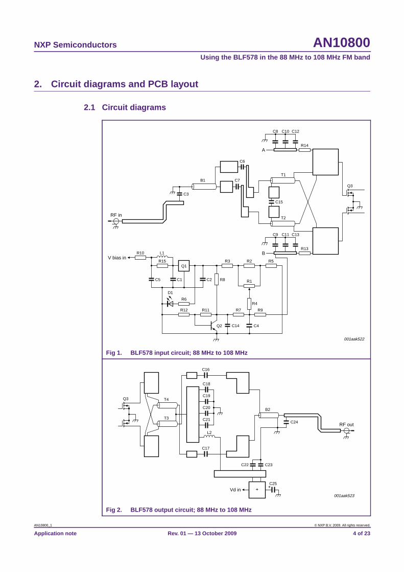
2. Circuit diagrams and PCB layout
2.1 Circuit diagrams
Fig 1. BLF578 input circuit; 88 MHz to 108 MHz
Fig 2. BLF578 output circuit; 88 MHz to 108 MHz
001aak522
R10
R6
D1
R15 R3
R8
R4
C4
R12 R11 R7
R1
R2 R5
R9
L1
C5 C1 C2
C14Q2
C3
C12
R14
C10C8
C15
B1T1
T2
C7
C6
A
C13
R13
Q3
C11C9
B
RF in
V bias in
Q1
RF out
Vd in
T4
T3
B2
C25
C18
C19
C20
C21
L2
C23
C24
C22
C17
C16
001aak523
Q3
+
AN10800_1 © NXP B.V. 2009. All rights reserved.
Application note Rev. 01 — 13 October 2009 4 of 23
NXP Semiconductors AN10800Using the BLF578 in the 88 MHz to 108 MHz FM band
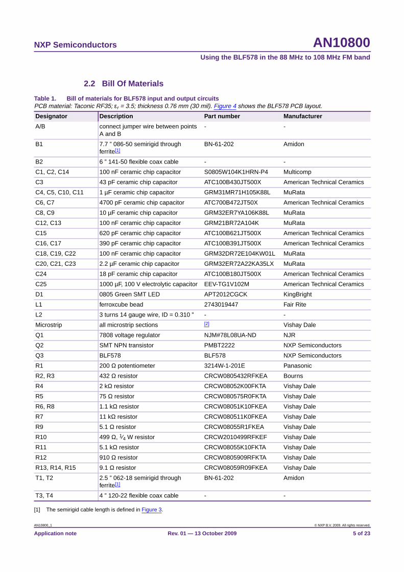
2.2 Bill Of Materials
[1] The semirigid cable length is defined in Figure 3.
Table 1. Bill of materials for BLF578 input and output circuitsPCB material: Taconic RF35; εr = 3.5; thickness 0.76 mm (30 mil). Figure 4 shows the BLF578 PCB layout.
Designator Description Part number Manufacturer
A/B connect jumper wire between pointsA and B
- -
B1 7.7 ” 086-50 semirigid throughferrite[1]
BN-61-202 Amidon
B2 6 ” 141-50 flexible coax cable - -
C1, C2, C14 100 nF ceramic chip capacitor S0805W104K1HRN-P4 Multicomp
C3 43 pF ceramic chip capacitor ATC100B430JT500X American Technical Ceramics
C4, C5, C10, C11 1 µF ceramic chip capacitor GRM31MR71H105K88L MuRata
C6, C7 4700 pF ceramic chip capacitor ATC700B472JT50X American Technical Ceramics
C8, C9 10 µF ceramic chip capacitor GRM32ER7YA106K88L MuRata
C12, C13 100 nF ceramic chip capacitor GRM21BR72A104K MuRata
C15 620 pF ceramic chip capacitor ATC100B621JT500X American Technical Ceramics
C16, C17 390 pF ceramic chip capacitor ATC100B391JT500X American Technical Ceramics
C18, C19, C22 100 nF ceramic chip capacitor GRM32DR72E104KW01L MuRata
C20, C21, C23 2.2 µF ceramic chip capacitor GRM32ER72A22KA35LX MuRata
C24 18 pF ceramic chip capacitor ATC100B180JT500X American Technical Ceramics
C25 1000 µF, 100 V electrolytic capacitor EEV-TG1V102M American Technical Ceramics
D1 0805 Green SMT LED APT2012CGCK KingBright
L1 ferroxcube bead 2743019447 Fair Rite
L2 3 turns 14 gauge wire, ID = 0.310 ” - -
Microstrip all microstrip sections [2] Vishay Dale
Q1 7808 voltage regulator NJM#78L08UA-ND NJR
Q2 SMT NPN transistor PMBT2222 NXP Semiconductors
Q3 BLF578 BLF578 NXP Semiconductors
R1 200 Ω potentiometer 3214W-1-201E Panasonic
R2, R3 432 Ω resistor CRCW0805432RFKEA Bourns
R4 2 kΩ resistor CRCW08052K00FKTA Vishay Dale
R5 75 Ω resistor CRCW080575R0FKTA Vishay Dale
R6, R8 1.1 kΩ resistor CRCW08051K10FKEA Vishay Dale
R7 11 kΩ resistor CRCW080511K0FKEA Vishay Dale
R9 5.1 Ω resistor CRCW08055R1FKEA Vishay Dale
R10 499 Ω, 1⁄4 W resistor CRCW2010499RFKEF Vishay Dale
R11 5.1 kΩ resistor CRCW08055K10FKTA Vishay Dale
R12 910 Ω resistor CRCW0805909RFKTA Vishay Dale
R13, R14, R15 9.1 Ω resistor CRCW08059R09FKEA Vishay Dale
T1, T2 2.5 ” 062-18 semirigid throughferrite[1]
BN-61-202 Amidon
T3, T4 4 ” 120-22 flexible coax cable - -
AN10800_1 © NXP B.V. 2009. All rights reserved.
Application note Rev. 01 — 13 October 2009 5 of 23

NXP Semiconductors AN10800Using the BLF578 in the 88 MHz to 108 MHz FM band
[2] Contact your local NXP Semiconductors’ salesperson for copies of the PCB layout files.
Fig 3. Cable length definition
001aak524
semirigid cable length
AN10800_1 © NXP B.V. 2009. All rights reserved.
Application note Rev. 01 — 13 October 2009 6 of 23

xxxx xxxxxxxxxxxxxxxxxxxxxxxxxxxxxx x xxxxxxxxxxxxxx xxxxxxxxxx xxx xxxxxx xxxxxxxxxxxxxxxxxxxxxxx xxxxxxxxxxxxxxxxxxxxxxxxxxx xxxxxx xx xxxxxxxxxxxxxxxxxxxxxxxxxxxxx xxxxxxxxxxxxxxxxxxxxxx xxxxxxxxxxx xxxxxxx xxxxxxxxxxxxxxxxxxxxxxxxxxxxxxxxxxx xxxxxxxxxxxxxx xxxxxx xx xxxxxxxxxxxxxxxxxxxxxxxxxxxxxxxx xxxxxxxxxxxxxxxxxxxxxxxx xxxxxxxxxxxxxxxxxxxxxxxxxxxxxxxxxxxxxxxxxxxxxxxxxxxxx xxxxxxxxxxx xxxxx x x
AN
10800_1
Application note
NX
P S
emiconducto
2.3B
B2T4 rsAN
10800U
sing the BLF
578 in the 88 MH
z to 108 MH
z FM
band
LF578 P
CB
layout
001aak525
C25
C24
© N
XP
B.V. 2009. A
ll rights reserved.
Rev. 01 —
13 October 2009
7 of 23
Fig 4. BLF578 PCB layout
BLF574(1)
input-rev 330RF35
BLF574(1)
output-rev 330RF35
C3C6
C7
C4
D1
C1
R15 C2R12
Q2
R11
C14
B1
C8
C10
C15
C13
R13
R4
R1
R5
R2
R3
R6
Q1
A
C12Q3
R14
T1
T2
L1 R8 C5
C16
C18
L2C17
C22
C23T3
C19
C20
C21
R7R10 C11
C9
R9

NXP Semiconductors AN10800Using the BLF578 in the 88 MHz to 108 MHz FM band
2.4 PCB form factorCare has been taken to minimize board space for the design. Figure 5 shows how 1000 Wcan be generated in a space only as wide as the transistor itself.
3. Amplifier design
3.1 Mounting considerationsTo ensure good thermal contact, a heatsink compound (such as Dow Corning 340) shouldbe used when mounting the BLF578 in the SOT539A package to the heatsink. Improvedthermal contact is obtainable when the devices are soldered on to the heatsink. Thislowers the junction temperature at high operating power and results in slightly betterperformance.
When greasing the part down, care must be taken to ensure that the amount of grease iskept to an absolute minimum. The NXP Semiconductors’ website can be consulted forapplication notes on the recommended mounting procedure for this type of device.
3.2 Bias circuitA temperature compensated bias circuit is used and comprises the following:
An 8 V voltage regulator (Q1) supplies the bias circuit. The temperature sensor (Q2) mustbe mounted in good thermal contact with the device under test (Q3). The quiescentcurrent is set using a potentiometer (R1). The gate voltage correction is approximately−4.8 mV/°C to −5.0 mV/°C. The VGS range is also reduced using a resistor (R2).
Fig 5. Photograph of the BLF578 circuit board
001aak526
AN10800_1 © NXP B.V. 2009. All rights reserved.
Application note Rev. 01 — 13 October 2009 8 of 23

NXP Semiconductors AN10800Using the BLF578 in the 88 MHz to 108 MHz FM band
The −2.2 mV/°C at its base is generated by Q2. This is then multiplied up by theR11 : R12 ratio for a temperature slope (i.e. approximately −15 mV/°C). The multiplicationfunction provided by the transistor is the reason it is used rather than a diode. A portion ofthe −15 mV/°C is summed into the potentiometer (R1).
The amount of temperature compensation is set by resistor R4. The ideal value proved tobe 2 kΩ. The values of R9, R13 and R14 are not important for temperature compensation.However, they are used for baseband stability and to improve IMD asymmetry at lowerpower levels.
3.3 Amplifier alignmentThere are several points in the circuit that allow performance parameters to be readilytraded off against one another. In general, the following areas of the circuit have the mostimpact on the circuit performance.
Effect of changing the output capacitors (C16 and C17):
• This is a key tuning point in the circuit. This point has the strongest influence on thetrade-off between efficiency and output power at 1 dB gain compression (PL(1dB)).
Changing the frequency band:
• A demonstration was done with the BLF578, but the frequency of operation washigher, at 128 MHz. Table 2 shows how the capacitors and baluns were modified toraise the frequency. This table can be used as a guide if the desired frequency bandwere to be lower as well, by making equivalent changes in the opposite direction.
The high efficiency tuning set-up can be traded off against the PL(1dB) tuning set-up asindicated in Table 3.
Table 2. Increasing the operating frequency
Component 88 MHz to 108 MHz 128 MHz
Capacitors connected to theFET drains
0 pF 18 pF
C16, C17 390 pF 180 pF with 100 pF
Capacitors connected to outputbalun, C24
18 pF 20 pF
Output balun, B2 152.4 mm (6 ”) 50 Ω 101.6 mm (4 ”) 50 Ω
Table 3. High-efficiency tuning set-up and P L(1dB) tuning set-up trade-off
Component High-efficiency tuning set-up High P L(1dB) tuning set-up
Capacitors connected to theFET drains
24 pF not placed
C24 24 pF 18 pF
AN10800_1 © NXP B.V. 2009. All rights reserved.
Application note Rev. 01 — 13 October 2009 9 of 23

NXP Semiconductors AN10800Using the BLF578 in the 88 MHz to 108 MHz FM band
[1] In the 43 V case, the high-efficiency tuning set-up gets an extra 3 % efficiency at the expense of between0.5 dB and 0.7 dB in compression performance.
[2] In the 50 V case, trading in 2 % efficiency lessens the compression by more than 0.5 dB at 1 kW.
4. RF performance characteristics
4.1 Continuous waveThis application explores two possible tuning compromises:
• high-efficiency 43 V, 800 W
• high PL(1dB), 50 V 1 kW
A summary of the results for these tuning set-ups is shown in Table 5 and Table 6.
Table 4. Tuned efficiency and power performance
Parameter Frequency(MHz)
43 V[1] 50 V[2]
High-efficiencytuning set-up
HighPL(1dB)tuningset-up
High-efficiencytuning set-up
High P L(1dB)tuningset-up
Compression at800 W
88 3.3 dB 2.6 dB - -
98 2.5 dB 1.8 dB - -
108 2.0 dB 1.5 dB - -
Efficiency at 800 W 88 80 % 78 % - -
98 80 % 77 % - -
108 81 % 78 % - -
Compression at1 kW
88 - - 2.6 dB 1.0 dB
98 - - 1.2 dB 0.5 dB
108 - - 0.8 dB 0.3 dB
Efficiency at 1 kW 88 - - 75 % 77 %
98 - - 77 % 75 %
108 - - 78 % 76 %
Table 5. High-efficiency tuning set-up: 43 V, 800 WThis table summarizes the performance of the high-efficiency tuning set-up at IDq = 200 mA andTh = 25 °C.
Frequency (MHz) PL (W) G (dB) η (%)
88 800 24.1 81
98 800 24.8 80
108 800 25.5 81
AN10800_1 © NXP B.V. 2009. All rights reserved.
Application note Rev. 01 — 13 October 2009 10 of 23
NXP Semiconductors AN10800Using the BLF578 in the 88 MHz to 108 MHz FM band
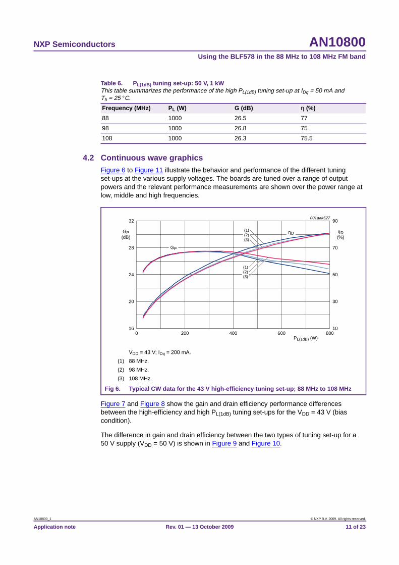
4.2 Continuous wave graphicsFigure 6 to Figure 11 illustrate the behavior and performance of the different tuningset-ups at the various supply voltages. The boards are tuned over a range of outputpowers and the relevant performance measurements are shown over the power range atlow, middle and high frequencies.
Figure 7 and Figure 8 show the gain and drain efficiency performance differencesbetween the high-efficiency and high PL(1dB) tuning set-ups for the VDD = 43 V (biascondition).
The difference in gain and drain efficiency between the two types of tuning set-up for a50 V supply (VDD = 50 V) is shown in Figure 9 and Figure 10.
Table 6. PL(1dB) tuning set-up: 50 V, 1 kWThis table summarizes the performance of the high PL(1dB) tuning set-up at IDq = 50 mA andTh = 25 °C.
Frequency (MHz) PL (W) G (dB) η (%)
88 1000 26.5 77
98 1000 26.8 75
108 1000 26.3 75.5
VDD = 43 V; IDq = 200 mA.
(1) 88 MHz.
(2) 98 MHz.
(3) 108 MHz.
Fig 6. Typical CW data for the 43 V high-efficiency tuning set-up; 88 MHz to 108 MHz
PL(1dB) (W)0 800600400200
001aak527
24
20
28
32
GP(dB)
16
50
30
70
90
ηD(%)
10
GP
ηD(1)(2)(3)
(1)(2)(3)
AN10800_1 © NXP B.V. 2009. All rights reserved.
Application note Rev. 01 — 13 October 2009 11 of 23

NXP Semiconductors AN10800Using the BLF578 in the 88 MHz to 108 MHz FM band
VDD = 43 V; IDq = 200 mA.
(1) 88 MHz high PL(1dB).
(2) 98 MHz high PL(1dB).
(3) 108 MHz high PL(1dB).
(4) 88 MHz high-efficiency.
(5) 98 MHz high-efficiency
(6) 108 MHz high-efficiency.
Fig 7. Gain comparison: 43 V, high-efficiency to high P L(1dB) tuning set-up
VDD = 43 V; IDq = 200 mA.
(1) 88 MHz high PL(1dB).
(2) 98 MHz high PL(1dB).
(3) 108 MHz high PL(1dB).
(4) 88 MHz high-efficiency.
(5) 98 MHz high-efficiency.
(6) 108 MHz high-efficiency.
Fig 8. Efficiency comparison: 43 V, high-efficiency to high P L(1dB) tuning set-ups
PL(1dB) (W)0 800600400200
001aak528
26
24
28
30
G(dB)
22
(1)(2)(3)(4)(5)(6)
PL(1dB) (W)0 800600400200
001aak529
50
30
70
90
ηD(%)
10
(1)(2)(3)(4)(5)(6)
AN10800_1 © NXP B.V. 2009. All rights reserved.
Application note Rev. 01 — 13 October 2009 12 of 23

NXP Semiconductors AN10800Using the BLF578 in the 88 MHz to 108 MHz FM band
VDD = 50 V; IDq = 50 mA.
(1) 88 MHz high PL(1dB).
(2) 98 MHz high PL(1dB).
(3) 108 MHz high PL(1dB).
(4) 88 MHz high-efficiency.
(5) 98 MHz high-efficiency.
(6) 108 MHz high-efficiency.
Fig 9. Gain comparison: 50 V, high-efficiency to high P L(1dB) tuning set-ups
VDD = 50 V; IDq = 50 mA.
(1) 88 MHz high PL(1dB).
(2) 98 MHz high PL(1dB).
(3) 108 MHz high PL(1dB).
(4) 88 MHz high-efficiency.
(5) 98 MHz high-efficiency.
(6) 108 MHz high-efficiency.
Fig 10. Efficiency comparison: 50 V, high-efficiency to high P L(1dB) tuning set-ups
PL(1dB) (W)0 1000800400 600200
001aak530
25
23
27
29
G(dB)
21
(1)(2)(3)(4)(5)(6)
PL(1dB) (W)0 1000800400 600200
001aak531
50
30
70
90
ηD(%)
10
(1)(2)(3)
(4)(5)(6)
AN10800_1 © NXP B.V. 2009. All rights reserved.
Application note Rev. 01 — 13 October 2009 13 of 23
NXP Semiconductors AN10800Using the BLF578 in the 88 MHz to 108 MHz FM band
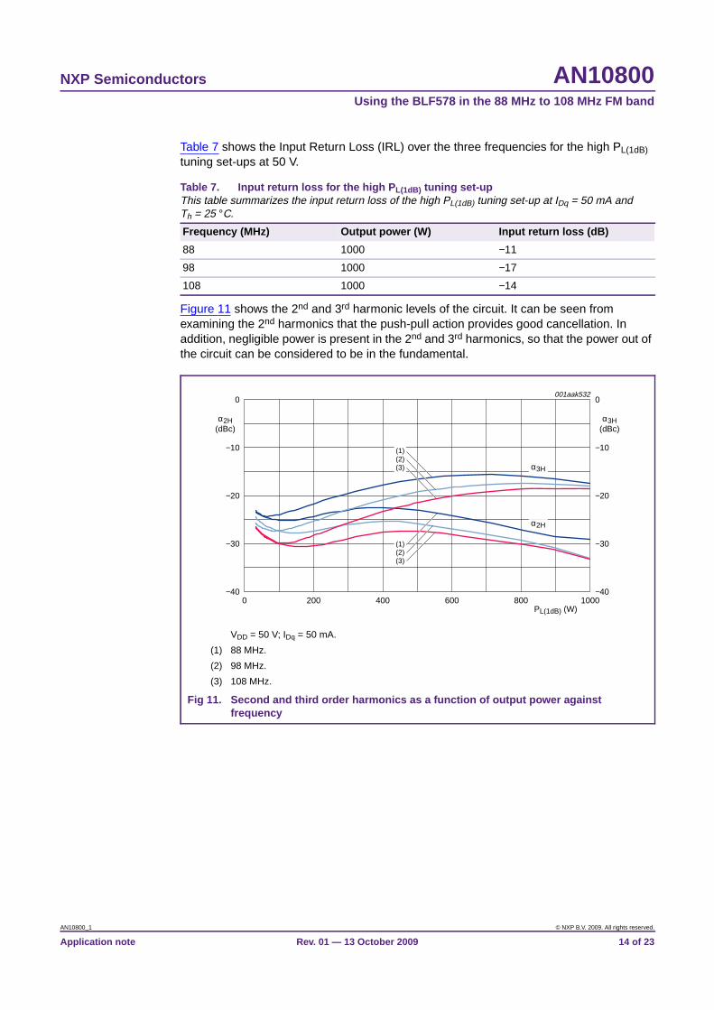
Table 7 shows the Input Return Loss (IRL) over the three frequencies for the high PL(1dB)tuning set-ups at 50 V.
Figure 11 shows the 2nd and 3rd harmonic levels of the circuit. It can be seen fromexamining the 2nd harmonics that the push-pull action provides good cancellation. Inaddition, negligible power is present in the 2nd and 3rd harmonics, so that the power out ofthe circuit can be considered to be in the fundamental.
Table 7. Input return loss for the high P L(1dB) tuning set-upThis table summarizes the input return loss of the high PL(1dB) tuning set-up at IDq = 50 mA andTh = 25 °C.
Frequency (MHz) Output power (W) Input return loss (dB)
88 1000 −11
98 1000 −17
108 1000 −14
VDD = 50 V; IDq = 50 mA.
(1) 88 MHz.
(2) 98 MHz.
(3) 108 MHz.
Fig 11. Second and third order harmonics as a function of output power againstfrequency
PL(1dB) (W)0 1000800400 600200
001aak532
−20
−30
−10
0
α2H(dBc)
−40
−20
−30
−10
0
α3H(dBc)
−40
(1)(2)(3)
(1)(2)(3)
α3H
α2H
AN10800_1 © NXP B.V. 2009. All rights reserved.
Application note Rev. 01 — 13 October 2009 14 of 23

NXP Semiconductors AN10800Using the BLF578 in the 88 MHz to 108 MHz FM band
5. Input and output impedance
The BLF578 input and output impedances are given in Table 8. These are generated froma first order equivalent circuit of the device and can be used to get the first-pass matchingcircuits.
The convention for these impedances is shown in Figure 12. They indicate theimpedances looking into half the device.
Table 8. Input and output impedance per section
Frequency (MHz) Input Output
Zi Zo
25 1.176 −j13.262 1.697 −j0.060
50 1.176 −j6.617 1.688 −j0.120
75 1.176 −j4.395 1.674 −j0.178
100 1.176 −j3.280 1.654 −j0.234
125 1.176 −j2.607 1.630 −j0.288
150 1.176 −j2.155 1.600 −j0.338
175 1.177 −j1.830 1.567 −j0.385
200 1.177 −j1.583 1.531 −j0.427
225 1.177 −j1.390 1.491 −j0.466
250 1.178 −j1.233 1.449 −j0.500
275 1.178 −j1.103 1.406 −j0.531
300 1.178 −j0.993 1.361 −j0.556
325 1.179 −j0.898 1.316 −j0.578
350 1.179 −j0.816 1.270 −j0.596
375 1.180 −j0.743 1.225 −j0.610
400 1.180 −j0.678 1.179 −j0.620
425 1.181 −j0.620 1.135 −j0.627
450 1.181 −j0.567 1.091 −j0.631
475 1.182 −j0.519 1.048 −j0.632
500 1.183 −j0.474 1.007 −j0.631
Fig 12. Impedance convention
001aak541
ZoZi
AN10800_1 © NXP B.V. 2009. All rights reserved.
Application note Rev. 01 — 13 October 2009 15 of 23
NXP Semiconductors AN10800Using the BLF578 in the 88 MHz to 108 MHz FM band
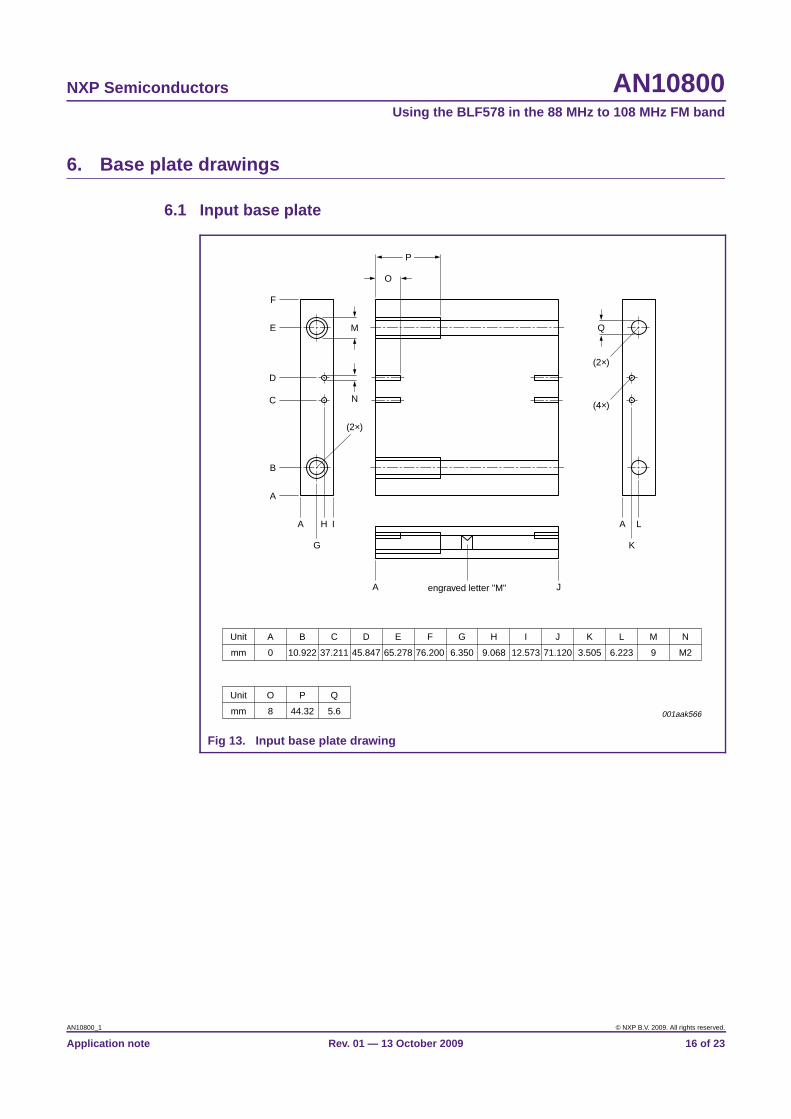
6. Base plate drawings
6.1 Input base plate
Fig 13. Input base plate drawing
001aak566
Unit
mm
A
0
B
10.922
C
37.211
D
45.847
E
65.278
F
76.200
G
6.350
H
9.068
I
12.573
J
71.120
Unit
mm
K
3.505
L
6.223
M
9
N
M2
O
8
P
44.32
Q
5.6
A
B
C
D
E
F
A
O
P
Q
N
(2×)
(2×)
(4×)
M
G
I
A engraved letter "M" J
A
K
LH
AN10800_1 © NXP B.V. 2009. All rights reserved.
Application note Rev. 01 — 13 October 2009 16 of 23

NXP Semiconductors AN10800Using the BLF578 in the 88 MHz to 108 MHz FM band
6.2 Device insert
(1) +0.5 mm.
Fig 14. Device insert drawing
001aak567
Unit
mm
A
0
B
10.922
C
65.278
D
76.200
E
6.350
F
11.328
G
5.156
H
10.312
I
4.978
J
11.328
K
10.185
L
1.143
M
8
N
M5(1)
Unit O
72.644
P
59.309
Q
23.749
U
0.254
V
10.058
R
3.556
S
3.5
T
M2.5
A
N
S
(2×)
(2×)
(2×)
T
A
HG A IA E
M
F
L
K
A
J
A
Q
P
O
R
B
C
D
engraved letter "M"
mm
VU
AN10800_1 © NXP B.V. 2009. All rights reserved.
Application note Rev. 01 — 13 October 2009 17 of 23
NXP Semiconductors AN10800Using the BLF578 in the 88 MHz to 108 MHz FM band
6.3 Output base plate
7. Reliability
At first glance, it would seem that great strains would be put on a single device running at800 W or even 1 kW of output power. Careful consideration to the die layout has helpedminimize these stresses, resulting in very reliable performance.
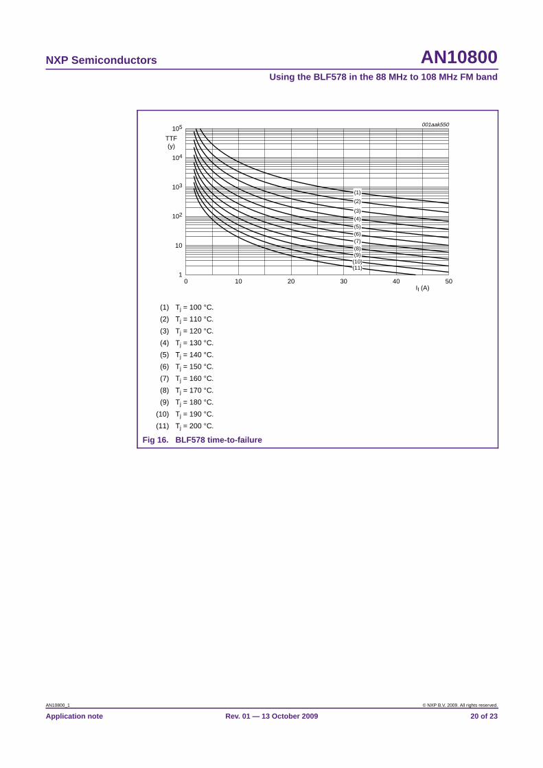
Time-to-Failure (TTF) is defined as the expected time elapsed until 0.1 % of the devices ofa sample size fail. This is different from Mean-Time-to-Failure (MTBF), where half thedevices would have failed and is orders of magnitude are shorter. The predominant failuremode for LDMOS devices is electromigration. The TTF for this mode is primarilydependant on junction temperature (Tj). Once the device junction temperature ismeasured and an in-depth knowledge is obtained for the average operating current for theapplication, the TTF can be calculated using Figure 16 and the related procedure.
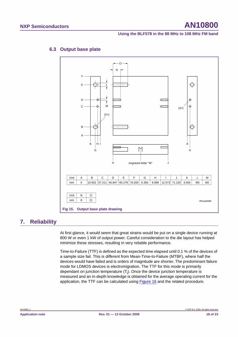
Fig 15. Output base plate drawing
001aak568
Unit
mm
A
0
B
10.922
C
37.211
D
45.847
E
65.278
F
76.200
G
6.350
H
9.068
I
12.573
J
71.120
Unit
mm
K
3.505
L
M5
M
M2
N
8
O
21
A
B
C
D
E
F
A
N
O
M
(2×)
(4×)
L
G
I
A engraved letter "M" J
A
K
H
AN10800_1 © NXP B.V. 2009. All rights reserved.
Application note Rev. 01 — 13 October 2009 18 of 23
NXP Semiconductors AN10800Using the BLF578 in the 88 MHz to 108 MHz FM band
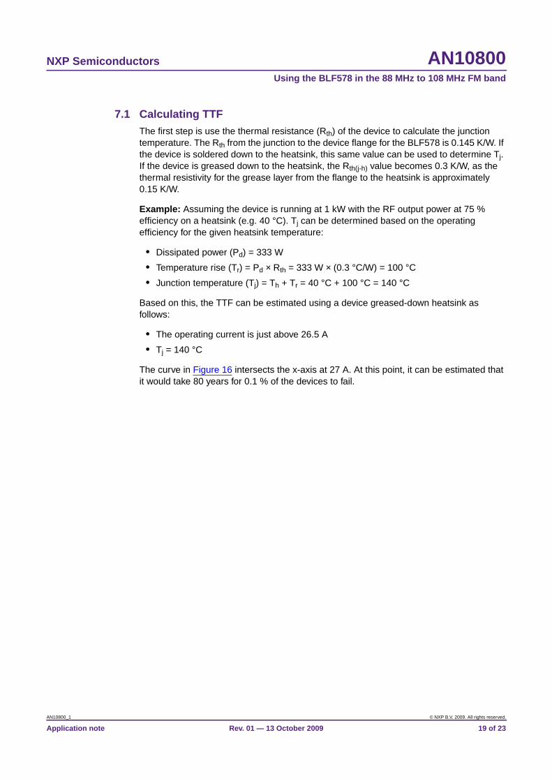
7.1 Calculating TTFThe first step is use the thermal resistance (Rth) of the device to calculate the junctiontemperature. The Rth from the junction to the device flange for the BLF578 is 0.145 K/W. Ifthe device is soldered down to the heatsink, this same value can be used to determine Tj.If the device is greased down to the heatsink, the Rth(j-h) value becomes 0.3 K/W, as thethermal resistivity for the grease layer from the flange to the heatsink is approximately0.15 K/W.
Example: Assuming the device is running at 1 kW with the RF output power at 75 %efficiency on a heatsink (e.g. 40 °C). Tj can be determined based on the operatingefficiency for the given heatsink temperature:
• Dissipated power (Pd) = 333 W
• Temperature rise (Tr) = Pd × Rth = 333 W × (0.3 °C/W) = 100 °C
• Junction temperature (Tj) = Th + Tr = 40 °C + 100 °C = 140 °C
Based on this, the TTF can be estimated using a device greased-down heatsink asfollows:
• The operating current is just above 26.5 A
• Tj = 140 °C
The curve in Figure 16 intersects the x-axis at 27 A. At this point, it can be estimated thatit would take 80 years for 0.1 % of the devices to fail.
AN10800_1 © NXP B.V. 2009. All rights reserved.
Application note Rev. 01 — 13 October 2009 19 of 23
NXP Semiconductors AN10800Using the BLF578 in the 88 MHz to 108 MHz FM band
(1) Tj = 100 °C.
(2) Tj = 110 °C.
(3) Tj = 120 °C.
(4) Tj = 130 °C.
(5) Tj = 140 °C.
(6) Tj = 150 °C.
(7) Tj = 160 °C.
(8) Tj = 170 °C.
(9) Tj = 180 °C.
(10) Tj = 190 °C.
(11) Tj = 200 °C.
Fig 16. BLF578 time-to-failure
001aak550
102
10
104
103
105
TTF(y)
1
II (A)0 504020 3010
(1)
(2)
(3)(4)(5)(6)(7)
(9)
(11)
(8)
(10)
AN10800_1 © NXP B.V. 2009. All rights reserved.
Application note Rev. 01 — 13 October 2009 20 of 23

NXP Semiconductors AN10800Using the BLF578 in the 88 MHz to 108 MHz FM band
8. Test configuration block diagram
9. PCB layout diagrams
Please contact your local NXP Semiconductors’ salesperson for copies of the PCB layoutfiles.
10. Abbreviations
Fig 17. BLF578 test configuration
001aak556
SPECTRUMANALYZER
Rhode & SchwarzFSEB
POWERMETERE4419B
POWERSENSORHP8481A
SPINNERSWITCH
DRIVERAMPLIFIEROphir 5127
COUPLERHP778D
RF COAXIALATTENUATOR
Tenuline30 dB1 kW
DUAL COAXIALDIRECTIONAL
COUPLERNarda3020A
10 dBPAD
DUT
3 dBPAD
RF FILTERBird 220 MHz
POWERSENSORHP8481A
SIGNALGENERATOR
SMIQ 03
Table 9. Abbreviations
Acronym Description
CW Continuous Wave
ESD ElectroStatic Discharge
FM Frequency Modulation
IMD InterModulation Distortion
IRL Input Return Loss
LDMOST Laterally Diffused Metal-Oxide Semiconductor Transistor
PAR Peak-to-Average power Ratio
PCB Printed-Circuit Board
SMT Surface Mount Technology
VHF Very High Frequency
VSWR Voltage Standing Wave Ratio
AN10800_1 © NXP B.V. 2009. All rights reserved.
Application note Rev. 01 — 13 October 2009 21 of 23
NXP Semiconductors AN10800Using the BLF578 in the 88 MHz to 108 MHz FM band
11. Legal information
11.1 Definitions
Draft — The document is a draft version only. The content is still underinternal review and subject to formal approval, which may result inmodifications or additions. NXP Semiconductors does not give anyrepresentations or warranties as to the accuracy or completeness ofinformation included herein and shall have no liability for the consequences ofuse of such information.
11.2 Disclaimers
General — Information in this document is believed to be accurate andreliable. However, NXP Semiconductors does not give any representations orwarranties, expressed or implied, as to the accuracy or completeness of suchinformation and shall have no liability for the consequences of use of suchinformation.
Right to make changes — NXP Semiconductors reserves the right to makechanges to information published in this document, including withoutlimitation specifications and product descriptions, at any time and withoutnotice. This document supersedes and replaces all information supplied priorto the publication hereof.
Suitability for use — NXP Semiconductors products are not designed,authorized or warranted to be suitable for use in medical, military, aircraft,space or life support equipment, nor in applications where failure ormalfunction of an NXP Semiconductors product can reasonably be expectedto result in personal injury, death or severe property or environmentaldamage. NXP Semiconductors accepts no liability for inclusion and/or use ofNXP Semiconductors products in such equipment or applications andtherefore such inclusion and/or use is at the customer’s own risk.
Applications — Applications that are described herein for any of theseproducts are for illustrative purposes only. NXP Semiconductors makes norepresentation or warranty that such applications will be suitable for thespecified use without further testing or modification.
Export control — This document as well as the item(s) described hereinmay be subject to export control regulations. Export might require a priorauthorization from national authorities.
11.3 TrademarksNotice: All referenced brands, product names, service names and trademarksare the property of their respective owners.
AN10800_1 © NXP B.V. 2009. All rights reserved.
Application note Rev. 01 — 13 October 2009 22 of 23

NXP Semiconductors AN10800Using the BLF578 in the 88 MHz to 108 MHz FM band
12. Figures
Fig 1. BLF578 input circuit; 88 MHz to 108 MHz . . . . . . .4Fig 2. BLF578 output circuit; 88 MHz to 108 MHz . . . . . .4Fig 3. Cable length definition . . . . . . . . . . . . . . . . . . . . . .6Fig 4. BLF578 PCB layout . . . . . . . . . . . . . . . . . . . . . . . .7Fig 5. Photograph of the BLF578 circuit board . . . . . . . .8Fig 6. Typical CW data for the 43 V high-efficiency
tuning set-up; 88 MHz to 108 MHz . . . . . . . . . . .11Fig 7. Gain comparison: 43 V, high-efficiency
to high PL(1dB) tuning set-up. . . . . . . . . . . . . . . . .12Fig 8. Efficiency comparison: 43 V, high-efficiency
to high PL(1dB) tuning set-ups . . . . . . . . . . . . . . . .12Fig 9. Gain comparison: 50 V, high-efficiency to high
PL(1dB) tuning set-ups . . . . . . . . . . . . . . . . . . . . . 13Fig 10. Efficiency comparison: 50 V, high-efficiency
to high PL(1dB) tuning set-ups. . . . . . . . . . . . . . . . 13Fig 11. Second and third order harmonics as a
function of output power against frequency. . . . . 14Fig 12. Impedance convention . . . . . . . . . . . . . . . . . . . . 15Fig 13. Input base plate drawing . . . . . . . . . . . . . . . . . . . 16Fig 14. Device insert drawing . . . . . . . . . . . . . . . . . . . . . 17Fig 15. Output base plate drawing. . . . . . . . . . . . . . . . . . 18Fig 16. BLF578 time-to-failure . . . . . . . . . . . . . . . . . . . . . 20Fig 17. BLF578 test configuration . . . . . . . . . . . . . . . . . . 21
13. Contents
1 Introduction . . . . . . . . . . . . . . . . . . . . . . . . . . . . 32 Circuit diagrams and PCB layout . . . . . . . . . . . 42.1 Circuit diagrams . . . . . . . . . . . . . . . . . . . . . . . . 42.2 Bill Of Materials . . . . . . . . . . . . . . . . . . . . . . . . 52.3 BLF578 PCB layout . . . . . . . . . . . . . . . . . . . . . 72.4 PCB form factor . . . . . . . . . . . . . . . . . . . . . . . . 83 Amplifier design. . . . . . . . . . . . . . . . . . . . . . . . . 83.1 Mounting considerations. . . . . . . . . . . . . . . . . . 83.2 Bias circuit . . . . . . . . . . . . . . . . . . . . . . . . . . . . 83.3 Amplifier alignment . . . . . . . . . . . . . . . . . . . . . . 94 RF performance characteristics . . . . . . . . . . . 104.1 Continuous wave . . . . . . . . . . . . . . . . . . . . . . 104.2 Continuous wave graphics . . . . . . . . . . . . . . . 115 Input and output impedance. . . . . . . . . . . . . . 156 Base plate drawings . . . . . . . . . . . . . . . . . . . . 166.1 Input base plate . . . . . . . . . . . . . . . . . . . . . . . 166.2 Device insert . . . . . . . . . . . . . . . . . . . . . . . . . . 176.3 Output base plate . . . . . . . . . . . . . . . . . . . . . . 187 Reliability . . . . . . . . . . . . . . . . . . . . . . . . . . . . . 187.1 Calculating TTF . . . . . . . . . . . . . . . . . . . . . . . 198 Test configuration block diagram. . . . . . . . . . 219 PCB layout diagrams. . . . . . . . . . . . . . . . . . . . 2110 Abbreviations . . . . . . . . . . . . . . . . . . . . . . . . . . 2111 Legal information. . . . . . . . . . . . . . . . . . . . . . . 2211.1 Definitions . . . . . . . . . . . . . . . . . . . . . . . . . . . . 2211.2 Disclaimers . . . . . . . . . . . . . . . . . . . . . . . . . . . 2211.3 Trademarks . . . . . . . . . . . . . . . . . . . . . . . . . . . 2212 Figures . . . . . . . . . . . . . . . . . . . . . . . . . . . . . . . 2313 Contents . . . . . . . . . . . . . . . . . . . . . . . . . . . . . . 23
© NXP B.V. 2009. All rights reserved.For more information, please visit: http://www.nxp.comFor sales office addresses, please send an email to: [email protected]
Date of release: 13 October 2009
Document identifier: AN10800_1
Please be aware that important notices concerning this document and the product(s)described herein, have been included in section ‘Legal information’.