an nfc-connected coupler using ipt-cpt-combined wireless
TRANSCRIPT

IEEE TRANSACTIONS ON POWER ELECTRONICS, VOL. 36, NO. 6, JUNE 2021 6323
An NFC-Connected Coupler UsingIPT-CPT-Combined Wireless Charging for
Metal-Cover Smartphone ApplicationsJia-Qi Zhu, Yong-Ling Ban , Rui-Min Xu, Member, IEEE, and Chunting Chris Mi , Fellow, IEEE
Abstract—A near field communication (NFC)-connected couplerusing inductive power transfer (IPT)-capacitive power transfer(CPT)-combined wireless charging is proposed for metal-coversmartphone applications. To mitigate eddy current loss in the metalcover, CPT is introduced. Compared with traditional CPT, wirelesspower transfer through a metal cover is realized, and cost andvaluable space inside the smartphone are saved. To achieve CPTthrough a metal cover, the metal cover itself is separated by across slot and utilized as receiving plates. To reduce the voltageacross the metal cover within a safety range, IPT is applied. Thealready-existing NFC antenna is first used as the receiving coilfor IPT and also performs as the compensated inductance forCPT. By connecting one of its feed lines to the metal cover, onlya parallel external capacitor is needed to construct the receiver ofthe proposed coupler because the metal cover and NFC antennaare components that already exist inside the smartphone, whichgreatly saves space inside the smartphone and cost for the proposedcoupler. Prototypes of the proposed NFC-connected coupler withand without actual smartphone have been built. The wireless powertransfer through metal cover by IPT and CPT has been validatedvia experiment.
Index Terms—Capacitive power transfer (CPT), inductive powertransfer (IPT), metal cover, near field communication (NFC),smartphone application.
I. INTRODUCTION
W IRELESS power transfer (WPT) is a user-friendlycharging technology for consumer electronic devices,
which utilizes electromagnetic field to transfer power without an
Manuscript received June 28, 2020; revised September 12, 2020; acceptedOctober 23, 2020. Date of publication November 6, 2020; date of current versionFebruary 5, 2021. This work was supported in part by the National NaturalScience Foundation of China under Grant 61471098, in part by the NationalHigher-Education Institution General Research and Development Project un-der Grants ZYGX2016J035 and ZYGX2018J037, and in part by the ChinaScholarship Council. Recommended for publication by Associate Editor M.Ponce-Silva. (Corresponding authors: Yong-Ling Ban; Chunting Chris Mi.)
Jia-Qi Zhu is with the School of Electronic Engineering, University ofElectronic Science and Technology of China, Chengdu 611731, China, and alsowith the Department of Electrical and Computer Engineering, San Diego StateUniversity, San Diego, CA 92182 USA (e-mail: [email protected]).
Yong-Ling Ban and Rui-Min Xu are with the School of Electronic Engi-neering, University of Electronic Science and Technology of China, Chengdu611731, China (e-mail: [email protected]; [email protected]).
Chunting Chris Mi is with the Department of Electrical and ComputerEngineering, San Diego State University, San Diego, CA 92182 USA (e-mail:[email protected]).
Color versions of one or more of the figures in this article are available onlineat https://ieeexplore.ieee.org.
Digital Object Identifier 10.1109/TPEL.2020.3036459
electric contact [1]. In recent years, with the rapid expansion ofthe smartphone market, integrating a WPT coupler into a mobilehandset is now becoming a necessity due to its advantages ofbeing cordless, waterproof and user friendly over a conventionalplug-in charger [2]. With regard to nonmetallic-cover smart-phones, inductive power transfer (IPT) is widely applied withQi standard [3]–[5]. However, for metal-cover smartphones,eddy current will be induced and the magnetic field lines willbe blocked by the metal cover, resulting in low power andefficiency [6], [7]. In this case, capacitive power transfer (CPT)is a good alternative because the electric field generated by thecapacitive coupler does not induce significant eddy-current lossin nearby metal objects [8]–[10]. Since two separate metal platesare needed for a receiving capacitive coupler, the metal coveritself can be utilized as receiving plates and no metal barrier issandwiched between the transmitter and receiver. Here, peoplemay touch the metal cover during the charging process so that thevoltage on the metal cover needs to be constrained within a safetyrange, which is 8.35 V for high frequency (HF) applications[11]–[13]. Nevertheless, if only capacitive charging is applied,it is hard to limit the voltage on the metal cover within a safetyrange because the CPT capability is in proportion to the voltageacross the metal plates. In this circumstance, if both IPT andCPT are applied to transfer power, eddy current loss can bemitigated and voltage on the metal cover can be reduced withina safety range. Besides, an IPT-CPT-combined coupler cansignificantly save valuable space inside a compact smartphonebecause the inductive coil of IPT can also be utilized as thecompensation inductance for CPT and vice versa. Above all,IPT-CPT-combined wireless charging is a promising technologyfor metal-cover smartphones.
Both inductive and capacitive couplers can be classified by cir-cuit topology. The inductive coupler can be classified as series-none (SN) topology [14], double-sided series or parallel topol-ogy (series–series, series–parallel, parallel–series, and parallel–parallel) [15], and double-sided LCC-compensated topology[16]. Similar to the inductive coupler, the capacitive couplercan be classified by its compensation topology and the corre-sponding characteristics are introduced as follows. The mostcommon topology for capacitive coupler is the SN topology,in which only one series inductance is placed at either thetransmitter or receiver side to compensate the coupling capac-itance generated by metal plates [17], [18]. In this topology, alarge coupling capacitance is required to achieve a reasonable
0885-8993 © 2020 IEEE. Personal use is permitted, but republication/redistribution requires IEEE permission.See https://www.ieee.org/publications/rights/index.html for more information.
Authorized licensed use limited to: San Diego State University. Downloaded on February 06,2021 at 03:23:12 UTC from IEEE Xplore. Restrictions apply.

6324 IEEE TRANSACTIONS ON POWER ELECTRONICS, VOL. 36, NO. 6, JUNE 2021
switching frequency, leading to a small gap distance betweenthe transmitter and receiver. A double-sided LCLC compensatedtopology was proposed in [9] and a 2.4-kW output power wastransferred through a 150-mm air gap with 90.8% efficiency. Toreduce the external compensated components, a double-sidedLC compensated topology is investigated in [19]. A 150-Wloosely coupled CPT system of 2.16% coupling coefficient wasachieved with 180 mm air gap distance and the correspondingefficiency was higher than 70%. Different from [19], in thisarticle, the compensated inductance is also used to transferpower, leading to an IPT-CPT-combined coupler which savesspace and cost. Besides, the external parallel capacitances at thetransmitter and the receiver side are different to adjust the powertransfer ratio between IPT and CPT.
By reviewing IPT, CPT, and IPT-CPT combined systems,[20] depicted the advantages of IPT-CPT-combined systemon power scaling capability, reduced compensation elements,higher link power transfer density, less pad compatibility issues,and improved misalignment tolerance, which indicates the ne-cessity and imminent trend to combine IPT and CPT. Severaltechniques to achieve WPT through inductive and capacitivecoupling have been investigated recently. As reported in [21]and [22], IPT-CPT-combined systems with LC-compensatedtopology were proposed for high power applications such aselectric vehicles. In these two studies, the inductive coils forIPT and metallic plates for CPT are separately placed with abig air gap, indicating that the IPT coupler and CPT couplerare actually not integrated. The size of the combined coupleris the sum of the capacitive coupler and the inductive coupler.Besides, an inductive coil and two metal plates are requiredto be integrated at the receiving side. Thus, the systems in[21] and [22] are not suitable to be integrated into a compactsmartphone. An inductive and capacitive integrated coupler withLCL compensation topology was studied in [23]. Both magneticfield and electric field were utilized in a single integrated coupler.However, the long-folded strip structure with 36 mm height wastoo large for smartphone applications and an external compen-sated inductance was required to adjust the power transfer ratioof IPT and CPT, which did not meet the compact requirement ofa smartphone. In [24], an integrated IPT-CPT combined couplerwas investigated for railway application. The metal plates werevertically arranged, and the coils were sandwiched between themetal plates. Although good misalignment ability is realized,this type of integrated coupler is not suitable for metal-coversmartphones because of the vertically arranged metal plates thatcannot be used as metal cover, the 20-mm distance betweenthe receiving coil and metal plate, as well as the eddy currentloss without embedded ferrite. In [25] and [26], inductive andcapacitive combined systems were reported for parallel trans-mission of power and data. In [25], the power is transferredby an electric field and in [26], the power is transferred bya tightly coupled transformer. Since the power and data wereseparately transferred by IPT and CPT, these systems are notdedicated to transfer power by magnetic field and electric fieldsimultaneously. As indicated in [27], a distance-insensitive WPTsystem was proposed using mixed inductive and capacitive cou-pling. The magnetic coupling coefficient and electric couplingcoefficient canceled each other so that the equivalent coupling
coefficient in close range would be reduced, which suppressedfrequency splitting phenomenon at small transmitting distance.The above-mentioned systems were all operated in free spacecondition. To achieve WPT through a metal barrier, a combinedinductive and capacitive coupler was investigated in [28]. Twoseparate transmitting plates were employed to induce currentflow in the metal barrier, thus generating a magnetic field on thesecondary side. Here, the magnetic field was a horizontal-fluxapproach so that the pick-up coil inside the receiver was requiredto be perpendicular to the metal barrier, which was not suitablefor smartphone applications. Besides, the size of the secondarycompensating circuit was too big to be embedded in a mobileelectronic device.
In [29], an NFC-CPT-combined coupler was proposed formetal-cover smartphone applications. Except for the structuresof NFC antenna and metal plates, the proposed NFC-connectedcoupler in this article is completely different from the couplerin [29]. We need to emphasize here that the structures of theNFC antenna and metal plates (similar with [29]) are viewed ascomponents that are already designed and existing in the pro-posed NFC-connected coupler. The main differences between[29] and the proposed coupler are indicated as follows. First, thecoupler structures are different. An NFC antenna is connectedto the metal plates (metal cover) in the proposed coupler, whichmakes the NFC antenna part of the WPT system. The power istransferred simultaneously by both the NFC antenna (IPT) andthe metal cover (CPT). With regard to [29], the NFC antenna isglued onto the metal cover, but they are not connected, indicatingthat the NFC antenna is not part of the WPT system. The poweris only transferred by the electric field between the metal plates(CPT). Besides, since the coupler in [29] only utilizes electricfield to transfer power, the coil L at the transmitter side is notintegrated with the coupler and it is only used for compensation.On the contrary, in this article, the Tx coil at the transmitter sideis integrated with the proposed coupler, which is more compactthan [29]. The Tx coil is used for both compensation and powertransfer. Second, the circuit topologies are different. In [29],an SN topology is applied to the capacitive coupler. As forthe proposed coupler in this study, two parallel capacitors areapplied at the primary and secondary side for compensation andadjusting the power transfer ratio. Due to the different structureand circuit topology, the corresponding analyses method anddesign procedure are different.
In this article, an NFC-connected coupler using IPT-CPTcombined wireless charging is proposed for metal-cover smart-phone applications. To achieve WPT through metal cover andreduce eddy current loss, the metal cover itself is utilized asreceiving plates for CPT. To constrain the voltage on the metalcover within a safety range, the compensated inductive coil forCPT is also used to transfer power, resulting in an IPT-CPT-combined coupler. Here, the NFC antenna first performs asthe compensated inductance for CPT and also transfers powerthrough the magnetic field, which has not been reported in anyopen literature based on our review. As the NFC-based mobilepayment is becoming popular, NFC antenna has become a pre-requisite component inside smartphones [30]. In the proposedcoupler, the NFC antenna and metal cover that already exist inthe smartphone are employed to be the receiving coil for IPT and
Authorized licensed use limited to: San Diego State University. Downloaded on February 06,2021 at 03:23:12 UTC from IEEE Xplore. Restrictions apply.
ZHU et al.: NFC-CONNECTED COUPLER USING IPT-CPT-COMBINED WIRELESS CHARGING 6325
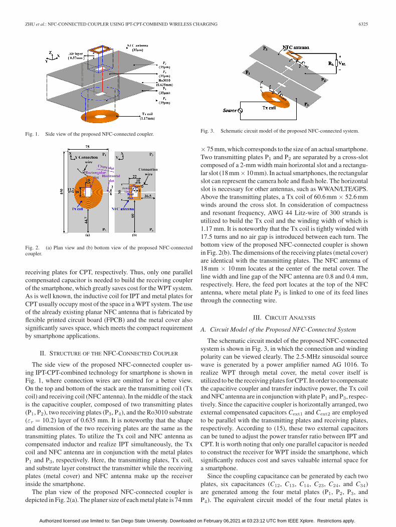
Fig. 1. Side view of the proposed NFC-connected coupler.
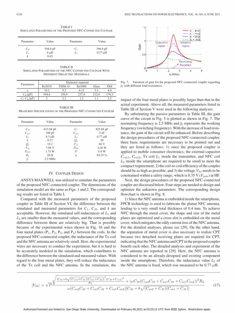
Fig. 2. (a) Plan view and (b) bottom view of the proposed NFC-connectedcoupler.
receiving plates for CPT, respectively. Thus, only one parallelcompensated capacitor is needed to build the receiving couplerof the smartphone, which greatly saves cost for the WPT system.As is well known, the inductive coil for IPT and metal plates forCPT usually occupy most of the space in a WPT system. The useof the already existing planar NFC antenna that is fabricated byflexible printed circuit board (FPCB) and the metal cover alsosignificantly saves space, which meets the compact requirementby smartphone applications.
II. STRUCTURE OF THE NFC-CONNECTED COUPLER
The side view of the proposed NFC-connected coupler us-ing IPT-CPT-combined technology for smartphone is shown inFig. 1, where connection wires are omitted for a better view.On the top and bottom of the stack are the transmitting coil (Txcoil) and receiving coil (NFC antenna). In the middle of the stackis the capacitive coupler, composed of two transmitting plates(P1, P2), two receiving plates (P3, P4), and the Ro3010 substrate(εr = 10.2) layer of 0.635 mm. It is noteworthy that the shapeand dimension of the two receiving plates are the same as thetransmitting plates. To utilize the Tx coil and NFC antenna ascompensated inductor and realize IPT simultaneously, the Txcoil and NFC antenna are in conjunction with the metal platesP1 and P3, respectively. Here, the transmitting plates, Tx coil,and substrate layer construct the transmitter while the receivingplates (metal cover) and NFC antenna make up the receiverinside the smartphone.
The plan view of the proposed NFC-connected coupler isdepicted in Fig. 2(a). The planer size of each metal plate is 74 mm
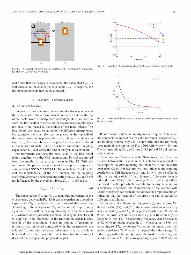
Fig. 3. Schematic circuit model of the proposed NFC-connected system.
× 75 mm, which corresponds to the size of an actual smartphone.Two transmitting plates P1 and P2 are separated by a cross-slotcomposed of a 2-mm width main horizontal slot and a rectangu-lar slot (18 mm× 10 mm). In actual smartphones, the rectangularslot can represent the camera hole and flash hole. The horizontalslot is necessary for other antennas, such as WWAN/LTE/GPS.Above the transmitting plates, a Tx coil of 60.6 mm × 52.6 mmwinds around the cross slot. In consideration of compactnessand resonant frequency, AWG 44 Litz-wire of 300 strands isutilized to build the Tx coil and the winding width of which is1.17 mm. It is noteworthy that the Tx coil is tightly winded with17.5 turns and no air gap is introduced between each turn. Thebottom view of the proposed NFC-connected coupler is shownin Fig. 2(b). The dimensions of the receiving plates (metal cover)are identical with the transmitting plates. The NFC antenna of18 mm × 10 mm locates at the center of the metal cover. Theline width and line gap of the NFC antenna are 0.8 and 0.4 mm,respectively. Here, the feed port locates at the top of the NFCantenna, where metal plate P3 is linked to one of its feed linesthrough the connecting wire.
III. CIRCUIT ANALYSIS
A. Circuit Model of the Proposed NFC-Connected System
The schematic circuit model of the proposed NFC-connectedsystem is shown in Fig. 3, in which the connection and windingpolarity can be viewed clearly. The 2.5-MHz sinusoidal sourcewave is generated by a power amplifier named AG 1016. Torealize WPT through metal cover, the metal cover itself isutilized to be the receiving plates for CPT. In order to compensatethe capacitive coupler and transfer inductive power, the Tx coiland NFC antenna are in conjunction with plate P1 and P3, respec-tively. Since the capacitive coupler is horizontally arranged, twoexternal compensated capacitors Cext1 and Cext2 are employedto be parallel with the transmitting plates and receiving plates,respectively. According to (15), these two external capacitorscan be tuned to adjust the power transfer ratio between IPT andCPT. It is worth noting that only one parallel capacitor is neededto construct the receiver for WPT inside the smartphone, whichsignificantly reduces cost and saves valuable internal space fora smartphone.
Since the coupling capacitance can be generated by each twoplates, six capacitances (C12, C13, C14, C23, C24, and C34)are generated among the four metal plates (P1, P2, P3, andP4). The equivalent circuit model of the four metal plates is
Authorized licensed use limited to: San Diego State University. Downloaded on February 06,2021 at 03:23:12 UTC from IEEE Xplore. Restrictions apply.

6326 IEEE TRANSACTIONS ON POWER ELECTRONICS, VOL. 36, NO. 6, JUNE 2021
Fig. 4. (a) Six capacitance model of the four metal plates (P1, P2, P3, andP4). (b) Simplified π model of the four metal plates.
Fig. 5. Equivalent circuit model of the proposed NFC-connected system.
shown in Fig. 4(a). Based on [10], the six capacitance modelcan be simplified as π model, which is constructed by couplingcapacitance CM and self-capacitance C1 and C2, as depicted inFig. 4(b). The relationship between the simplified π model andthe six capacitances generated among the four metal plates isdenoted as ⎧⎪⎪⎨
⎪⎪⎩C1 = C12 +
(C13+C14)·(C23+C24)C13+C14+C23+C24
C2 = C34 +(C13+C23)·(C14+C24)C13+C14+C23+C24
CM = C24C13−C14C23
C13+C14+C23+C24.
(1)
As the four metal plates are represented by its simplifiedπ model, the equivalent circuit model of the proposed systemis depicted in Fig. 5. Since the Tx coil and NFC antenna arein conjunction with metal plates P1 and P3, L1 represents theinductance of Tx coil and metal plate P1, and L2 representsthe inductance of NFC antenna and metal plate P3. Here, thepolarity of the Tx coil and NFC antenna is significant that theinductive power and capacitive power are superposed at theoutput. Otherwise, the inductive power and capacitive powerwill weaken each other if the polarities of the two coils arereversed.
B. Working Principle of the Circuit
Before analyzing the circuit of the proposed NFC-connectedsystem, capacitance Cin1 and Cin2 are defined as follows for
simplification: {Cin1 = C1 − CM + Cext1
Cin2 = C2 − CM + Cext2.(2)
To study the working principle of the proposed IPT-CPTsystem, Kirchhoff’s voltage law (KVL) is applied and the cor-responding equation is expressed as⎧⎨⎩
(jωL1 +1
jωCin1)I1 − 1
jωCin1I2 + jωMI3 = V1
− 1jωCin1
I1 + ( 1jωCin1
+ 1jωCM
+ 1jωCin2
)I2 − 1jωCin2
I3 = 0
jωMI1 − 1jωCin2
I2 + ( 1jωCin2
+ jωL2 +RL)I3 = 0.
(3)
By defining RCin1, RCin2, RCM, RL1, RL2 and RM as theimpedance of Cin1, Cin2, CM, L1, L2, and mutual inductanceM, the input current I1 and output current I3 are derived as (4),shown at the bottom of this page.
To achieve load-independent charging, RCin1(RCin2 +RCM ) + (RCin1 +RCin2 +RCM )RL1 needs to be zero andinductance L1 is thus derived as
L1 =Cin2 + CM
ω2(Cin2CM + Cin1CM + Cin1Cin2). (5)
To realize zero phase angle (ZPA) at the input, RCin2
(RCin1 +RCM ) + (RCin1 +RCin2 +RCM )RL2 should bezero and inductance L2 is obtained as
L2 =Cin1 + CM
ω2(Cin2CM + Cin1CM + Cin1Cin2). (6)
With (5) and (6), (4) can be simplified as
⎧⎪⎪⎪⎪⎪⎪⎪⎪⎪⎪⎪⎪⎪⎪⎪⎪⎪⎪⎪⎪⎪⎪⎪⎪⎪⎪⎪⎪⎪⎨⎪⎪⎪⎪⎪⎪⎪⎪⎪⎪⎪⎪⎪⎪⎪⎪⎪⎪⎪⎪⎪⎪⎪⎪⎪⎪⎪⎪⎪⎩
I1=V1(RCin1 +RCin2 +RCM )RL
RCin1RCin2(RCM+2RM)−(RCin1+RCin2+RCM)R2M
+RCin2RL1(RCM +RCin1)
= V1RL[(Cin2CM + Cin1CM + Cin1Cin2)ω
CM + (Cin2CM + Cin1CM + Cin1Cin2)ω2M]2
I2 =RCin1(RCin2 +RL +RL1)−RCin2RM
RCin1RCin2(RCM+2RM )−(RCin1+RCin2+RCM )R2M
+RCin2RL1(RCM +RCin1)ω2Cin2CM (Cin2CM + Cin1CM + Cin1Cin2)RL
=V1
−jωCin1CM [CM+ω2M(Cin2CM+Cin1CM+Cin1Cin2)]
[CM + (Cin2CM + Cin1CM + Cin1Cin2)ω2M ]2
I3=V1RCin1RCin2−RM (RCin1+RCin2+RCM )
RCin1RCin2(RCM+2RM)−(RCin1+RCin2+RCM)R2M
+RCin2RL1(RCM +RCin1)
= V1−jω(Cin2CM + Cin1CM + Cin1Cin2)
CM + (Cin2CM + Cin1CM + Cin1Cin2)ω2M.
(7)
⎧⎪⎪⎪⎪⎪⎪⎨⎪⎪⎪⎪⎪⎪⎩
I1 = V1RCin2(RCin1 +RCM ) + (RCin1 +RCin2 +RCM )(RL2 +RL)
RCin1RCin2(RCM +RL1 +RL2 + 2RM )− (RCin1 +RCin2 +RCM )(R2M +RL1RL2)
+RCM (RCin1RL2 +RCin2RL1) + [RCin1(RCin2 +RCM ) + (RCin1 +RCin2 +RCM )RL1]RL
I3 = V1RCin1(RCin2 −RM )−RM (RCin2 +RCM )
RCin1RCin2(RCM +RL1 +RL2 + 2RM )− (RCin1 +RCin2 +RCM )(R2M +RL1RL2)
+RCM (RCin1RL2 +RCin2RL1) + [RCin1(RCin2 +RCM ) + (RCin1 +RCin2 +RCM )RL1]RL
(4)
Authorized licensed use limited to: San Diego State University. Downloaded on February 06,2021 at 03:23:12 UTC from IEEE Xplore. Restrictions apply.

ZHU et al.: NFC-CONNECTED COUPLER USING IPT-CPT-COMBINED WIRELESS CHARGING 6327
Fig. 6. Equivalent behavior source model of the proposed NFC-connectedsystem.
From (7), the coil-to-coil efficiency η of the proposed systemcan be calculated as
η =I23RL
I21R1 + I23R2 + I23RL, (8)
where R1 and R2 are the resistance of Tx coil and NFC antenna,respectively.
Based on (7), the gain G of Fig. 5 can be derived as
G =
∣∣∣∣VRL
V1
∣∣∣∣ =∣∣∣∣I3RL
V1
∣∣∣∣=
ω(Cin2CM + Cin1CM + Cin1Cin2)RL
CM + (Cin2CM + Cin1CM + Cin1Cin2)ω2M. (9)
The voltage V12 across P1 and P2 and the voltage V34 acrossP3 and P4 can be deducted as
⎧⎪⎪⎪⎪⎪⎪⎪⎪⎪⎪⎪⎪⎪⎪⎨⎪⎪⎪⎪⎪⎪⎪⎪⎪⎪⎪⎪⎪⎪⎩
V12 = RCin1(I1 − I2)= RCin1V1
(RCin2 +RCM )RL − (RCin1RCin2 +RCin1RL1 −RCin2RM )
RCin1RCin2(RCM+2RM )−(RCin1+RCin2+RCM )R2M
+RCin2RL1(RCM +RCin1)V34 = RCin2(I2 − I3)= RCin2V1
RCin1RL +RCin1RL1 +RM (RCin1 +RCM )
RCin1RCin2(RCM + 2RM )−(RCin1+RCin2+RCM )R2M
+RCin2RL1(RCM +RCin1).(10)
In order to obtain the power PIPT transferred by the magneticfield and the power PCPT transferred by the capacitive field,the behavior source model of the system is depicted in Fig. 6.Compared with the circuit model in Fig. 5, the magnetic couplingbetween the Tx coil and NFC antenna is represented by current-controlled voltage sources. The coupled voltage in each coildepends on the mutual inductance and the current flowing in the
other coil. Besides, the electric coupling among the four plates isrepresented by voltage-controlled current sources, whose valuedepends on the voltage at the other side. Here, the apparent powerSCPT transferred by capacitive field can be calculated as
SCPT = V12
(− 1
RCMV34
)∗. (11)
The symbol “∗” in (11) represents the complex conjugate.From (11), the real power PCPT is derived to be (12), shown atthe bottom of this page.
The apparent power SIPT transferred by magnetic field isexpressed as
SIPT = −RMI1I∗3. (13)
According to (13), the real power PIPT is calculated as (14),shown at the bottom of this page.
In the proposed system, inductive power and capacitive powerare transferred simultaneously, thus, the power transfer ratio issignificant to be studied. Based on (12) and (14), the powertransfer ratio R between IPT and CPT is derived as
R =PIPT
PCPT=
√(Cin1 + CM )(Cin2 + CM )
CMk. (15)
Since the metal cover is used to transfer power and it willprobably be touched by people during the charging process, thevoltage V34 across the metal cover should be constrained withina safety range. According to [11] and [12], the voltage on themetal cover should be smaller than 8.35 V at HF.
Assuming that the output power is fixed as P, the requiredinput voltage V1 is deducted as follows based on (5)–(7):
V1 =
√P
RL
CM + k√
(Cin1 + CM )(Cin2 + CM )
ω(Cin2CM + Cin1CM + Cin1Cin2). (16)
By substituting (16) into (10), the rms value of V34 can becalculated as (17), shown at the bottom of the next page.
From (17), the optimum load resistance to realize the smallestvoltage across the metal cover is derived as
RL =[CM + k
√(Cin2 + CM )(Cin1 + CM )](CM + Cin1)
ωCM (Cin2CM + Cin1CM + Cin1Cin2).
(18)
PCPT
= V 21
RCin1RCin2RL
RCM
(RCin1RCin2 +RCin1RL1 −RCin2RM )RCin1 + (RCin2 +RCM )(RCin1RL1 +RM (RCin1 +RCM ))
(RCin1RCin2(RCM + 2RM )− (RCin1 +RCin2 +RCM )R2M +RCin2RL1(RCM +RCin1))
2
(12)
PIPT = V 21
(RCin1 +RCin2 +RCM )[RCin1RCin2 −RM (RCin1 +RCin2 +RCM )]RMRL
(RCin1RCin2(RCM + 2RM )− (RCin1 +RCin2 +RCM )R2M +RCin2RL1(RCM +RCin1))
2 (14)
Authorized licensed use limited to: San Diego State University. Downloaded on February 06,2021 at 03:23:12 UTC from IEEE Xplore. Restrictions apply.
6328 IEEE TRANSACTIONS ON POWER ELECTRONICS, VOL. 36, NO. 6, JUNE 2021
TABLE ISIMULATED PARAMETERS OF THE PROPOSED NFC-CONNECTED COUPLER
TABLE IISIMULATED PARAMETERS OF THE NFC-CONNECTED COUPLER WITH
DIFFERENT DIELECTRIC MATERIALS
TABLE IIIMEASURED SPECIFICATIONS OF THE PROPOSED NFC-CONNECTED COUPLER
IV. COUPLER DESIGN
ANSYS MAXWELL was utilized to simulate the parametersof the proposed NFC-connected coupler. The dimensions of thesimulation model are the same as Figs. 1 and 2. The correspond-ing results are listed in Table I.
Compared with the measured parameters of the proposedcoupler in Table III of Section VI, the difference between thesimulated and measured parameters for C1, CM, and k areacceptable. However, the simulated self-inductances of L1 andL2 are smaller than the measured values, and the correspondingdifference between them are relatively big. That is possiblybecause of the experimental wires shown in Fig. 16 and thefour metal plates (P1, P2, P3, and P4) between the coils. In theproposed NFC-connected coupler, the inductance of the Tx coiland the NFC antenna are relatively small. Here, the experimentalwires are necessary to conduct the experiment, but it is hard tobe accurately modeled in the simulation, which contributes tothe difference between the simulated and measured values. Withregard to the four metal plates, they will reduce the inductanceof the Tx coil and the NFC antenna. In the simulation, the
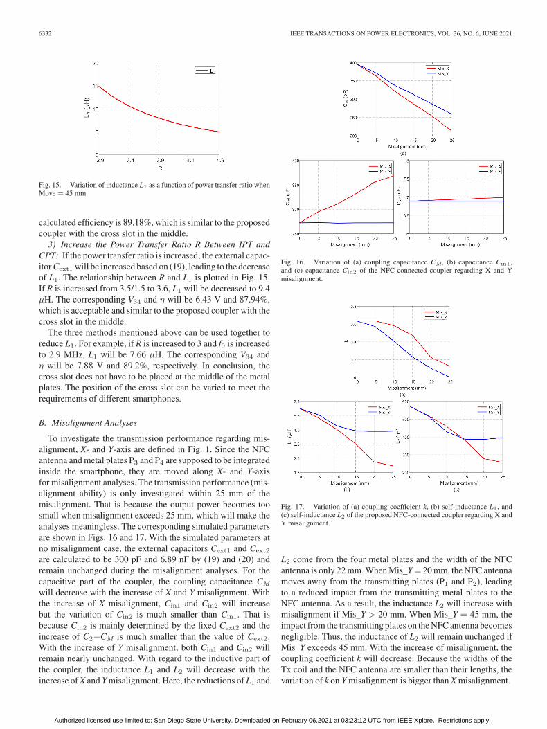
Fig. 7. Variation of gain for the proposed NFC-connected coupler regardingf0 with different load resistances.
impact of the four metal plates is possibly larger than that in theactual experiment. Above all, the measured parameters listed inTable III of Section V were used in the following analyses.
By substituting the passive parameters in Table III, the gaincurve of the circuit in Fig. 5 is plotted as shown in Fig. 7. Theresonating frequency is 2.5 MHz and f0 represents the workingfrequency (switching frequency). With the increase of load resis-tance, the gain of the circuit will be enhanced. Before describingthe design procedures of the proposed NFC-connected coupler,three basic requirements are necessary to be pointed out andthey are listed as follows: 1) since the proposed coupler isapplied to mobile consumer electronics, the external capacitorCext1, Cext2, Tx coil L1 inside the transmitter, and NFC coilL2 inside the smartphone are required to be small to meet thecompact requirement; 2) the coil-to-coil efficiency of the couplershould be as high as possible; and 3) the voltage V34 needs to beconstrained within a safety range, which is 8.35 V (Vsafe) at HF.
Next, the design procedures of the proposed NFC-connectedcoupler are discussed below. Four steps are needed to design andoptimize the unknown parameters. The corresponding designflowchart is shown in Fig. 8.
1) Since the NFC antenna is embedded inside the smartphone,FPCB technology is used to fabricate the planar NFC antenna,leading to a very small total thickness of 0.4 mm. To achieveNFC through the metal cover, the shape and size of the metalplates are optimized and a cross slot is embedded on the metalcover, which mitigates the eddy current loss of the NFC antenna.For the detailed analyses, please see [29]. On the other hand,the separation of metal cover is also necessary to realize CPTbecause two detached receiving plates are required for CPT,indicating that the NFC antenna and CPT in the proposed couplerbenefit each other. The detailed analyses and experiment of theNFC antenna are reported in [29]. Here, the NFC antenna isconsidered to be an already-designed and existing componentinside the smartphone. Therefore, the inductance value L2 ofthe NFC antenna is fixed, which was measured to be 0.77 μH.
|V34| =√P
√[CM+k
√(Cin2+CM )(Cin1+CM )]
2(CM+Cin1)
2
RL+ (ωCM (Cin2CM + Cin1CM + Cin1Cin2))
2RL
ω(Cin2CM + Cin1CM + Cin1Cin2)[CM + k√
(Cin2 + CM )(Cin1 + CM )](17)
Authorized licensed use limited to: San Diego State University. Downloaded on February 06,2021 at 03:23:12 UTC from IEEE Xplore. Restrictions apply.

ZHU et al.: NFC-CONNECTED COUPLER USING IPT-CPT-COMBINED WIRELESS CHARGING 6329
Fig. 8. Design flowchart of the proposed NFC-connected coupler.
2) According to (6) and (15), the external capacitor Cext1 andCext2 can be set to achieve the desired power transfer ratio. Theexternal capacitor Cext1 is thus expressed as
Cext1 = ω2L2
[(RCM
k
)2
− CM2
]− C1. (19)
The external capacitor Cext2 is expressed as
Cext2 =(RCM
k )2
ω2L2[(RCM
k )2 − CM
2]− C2. (20)
Here, the values of the external capacitors cannot be negative.With Cext1 ≥ 0
R ≥ k
√C1
ω2L2CM2 + 1 = Rmin. (21)
With Cext2 ≥ 0 and (21)(R
k
)2
(ω2L2C2 − 1) ≤ ω2L2C2. (22)
With L2 and C1 (C1 equals C2 due to symmetric property) ofTable III, the operating frequency needs to be 8.8 MHz to makeω2L2C2 − 1 = 0. Since the operating frequency of a wirelesscharging system is normally smaller than 6.78 MHz, ω2L2C2 −1 ≤ 0. Equation (22) can be conducted as(
R
k
)2
≥ −ω2L2C2
(1− ω2L2C2)(23)
which is always true. With the parameters in Table III, R isrequired to be bigger or equal to 2.14 by (21). As indicatedin Fig. 8, this requirement will be checked at the end of theprocedure.
Since CM has little impact on V34, the voltage V34 as a functionof power transfer ratio R is plotted with different resonatingfrequency and load resistance, as shown in Fig. 9(a). The outputpower for Fig. 9(a) is fixed as 5.6 W. According to the abovediscussion, the voltage V34 is required to be smaller than Vsafe.Based on (21), the power transfer ratio R is required to be biggerthan Rmin and the load resistance RL is not related to Rmin. With
Fig. 9. (a) Variation of voltage V34 across the metal cover as a functionof R with different resonating frequency and load resistance. (b) Coil-to-coilefficiency η as a function of R with different load resistances.
the increase of resonating frequency, Rmin will be decreased.As shown in Fig. 9(a), the voltage V34 is decreased with theincrease of R. That is because the voltage V34 across the metalcover is in proportion to the power transfer through CPT basedon (11). In order to limit the voltage across the metal coverwithin a safety range and provide a wider tunable range for f0and RL in the following steps, the power transfer ratio should beincreased. If R is tuned to be small, the resonating frequency mustbe increased because Rmin can be decreased with the increaseof f0. However, the increase of f0 will lead to increased V34. Forexample, if R is set below 2, the resonating frequency must be 3or 3.5 MHz to decrease Rmin in Fig. 9(a). In this case, the voltageV34 for the blue curve and magenta curve are above Vsafe, whichis not allowed. To fix this issue, the load resistance RL can beincreased, as shown in the green curve. However, the efficiencywill decrease significantly with the increase of load resistance, asdepicted in Fig. 9(b). Here, the resonating frequency for Fig. 9(b)is 3.5 MHz. For other resonating frequencies, similar resultscan be obtained in the required region (R > Rmin). Thus, Rcannot be too small and needs to be increased. On the otherhand, the current flowing in the Tx coil and the NFC antenna arein proportion to the power transferred by IPT based on (13). Withthe increase of current in the coils, the induced eddy current onthe metal plates will increase, leading to increased loss [31]. Ifthe coupler is integrated with a smartphone, more eddy currentloss will be induced on the nearby metallic components insidethe smartphone, leading to further decreased efficiency. Besides,with a fixed output power, the loss of the Tx coil will be increaseddue to the increase of input current I1 (increased R), resulting ina lower efficiency of the proposed coupler, which is verified inFig. 9(b). Therefore, the power transfer ratio should be reducedto increase efficiency. In consideration of both safety and eddycurrent loss, the power transfer ratio between IPT and CPT isselected to be 3.5/1.5.
3) Based on (2), (5), (19), and (20), L1 is determined byC1–CM, CM, and f0 due to the symmetric property. Since thedimension of the proposed coupler is set in step 1), the proposedcoupler is investigated with different dielectric materials, aslisted in Table II. Compared with coupling capacitance CM, thevalue change in C1–CM is much smaller regarding the dielectriclayer. The inductance L1 is thus determined by CM and f0.
With the variation of CM, L1, η, V34, and Cext2 are calculatedby (5), (8), (17), and (20). The output power for Fig. 10(c) is fixed
Authorized licensed use limited to: San Diego State University. Downloaded on February 06,2021 at 03:23:12 UTC from IEEE Xplore. Restrictions apply.

6330 IEEE TRANSACTIONS ON POWER ELECTRONICS, VOL. 36, NO. 6, JUNE 2021
Fig. 10. Variation of (a) capacitance Cext2 inside the smartphone, (b) induc-tance L1 of the Tx coil, (c) voltage V34 across the metal cover, and (d) coil-to-coilefficiency η as a function of coupling capacitance CM with different resonatingfrequencies.
Fig. 11. Variation of (a) capacitance Cext2 inside the smartphone, (b) induc-tance L1 of the Tx coil, (c) voltage V34 across the metal cover, and (d) coil-to-coilefficiency η regarding load resistance RL and working frequency f0.
as 5.6 W. The corresponding results with different resonatingfrequencies are shown in Fig. 10. Only L1 changes significantlywith CM, whereas other three parameters nearly remain un-changed. According to Fig. 11, the operating frequency f0 isrelevant to Cext2, L1, V34, and η. Therefore, CM is first set byL1 in this step.
As shown in Fig. 10(b), if the coupling capacitance CM issmall, the inductance L1 will become large, making the Tx coiltoo large to be embedded in the transmitter. Thus, CM needs to beincreased to reduce the inductance of the Tx coil. The inductanceof L1 is required to be smaller than 10 μH in this design. It isnoteworthy that this upper limit for L1 can be increased if a ferrite
sheet is integrated into the transmitter. As shown in Fig. 10(c),V34 will exceed or reach Vsafe if the resonant frequency is 3and 3.5 MHz, indicating that f0 must be smaller than 3 MHz. Asshown in Fig. 10(b), to limit L1 within 10μH, CM must be biggerthan 263.5 pF, indicating that a dielectric layer is necessary to beintegrated in the transmitter. In this case, the available Ro3010and TMM 10 from Table II can be selected as the dielectricmaterial to achieve acceptable CM. Because higher CM leads tobigger tunable range for f0, the available Ro3010 dielectric layerwith 0.635 mm thickness is finally selected, leading to suitablemeasured CM of 413.9 pF. It is noteworthy that other dielectriclayers with different thicknesses can be applied as long as theresultant CM meets the requirement in Fig. 10(b) and (c).
4) Based on (5), (19), and (20), with the selected CM, C1, C2,and fixed L2, the parameters of the coupler can be set with theload resistance RL and resonating frequency f0. To find the op-timum value of load resistance RL and resonating frequency f0,the compensated external capacitor Cext2, inductance L1 of theTx coil, voltage V34 across the metal cover and the coil-to-coilefficiency η are studied. With the variation of load resistanceand resonating frequency, L1, η, V34, and Cext2are calculated by(5), (8), (17), and (20). The corresponding results are depicted inFig. 11(a)–(d), respectively. It is noteworthy that the equivalentresistance R1 of the Tx coil and R2 of the NFC antenna aretaken into consideration to obtain Fig. 11(d). From Fig. 11(a)and (b), it can be seen that the external capacitance Cext2 andinductance L1 are independent of RL. With the increase ofresonating frequency, Cext2 and L1 will first decrease sharply andthen decrease slowly. Besides, as shown in Fig. 11(c), the voltageacross the metal cover will increase with the enhancement ofresonating frequency, indicating that the resonating frequencycannot be too high. In consideration of both space and safety(voltage across the metal cover), the resonating frequency isfinally selected as 2.5 MHz.
As shown in Fig. 11(d), the optimum coil-to-coil efficiency ηappears at 13Ω load resistance with 2.5 MHz working frequency.However, the corresponding voltage V34 across the metal coverwill be 8.34 V, which almost exceeds the safety range. Asindicated in Fig. 11(c), the lowest V34 comes with 40 Ω loadresistance at 2.5 MHz working frequency but the correspondingcoil-to-coil efficiency η is relatively low as 84.5%. Above all, asuitable value of 20 Ω is used for load resistance RL, which liesbetween 13 and 40 Ω. The calculated corresponding voltage V34
and coil-to-coil efficiency η are 7.14 V and 89.6%, respectively.According to (21) of step 2), the power transfer ratio needs
to be bigger than k√
C1
ω2L2CM2 + 1 ≈ k
√1
ω2L2CM+ 1 in con-
sideration of Cext1. After selecting the operating frequency, theexternal capacitor Cext1 can be calculated by (19). Accordingto step 3), CM is required to be relatively big to decrease L1.Based on step 4), f0 cannot be too large in consideration of V34.
Thus, the value of k√
1ω2L2CM
+ 1 is relatively small and the
selected power transfer ratio will normally meet the requirementof (21). For example, the required minimum power transfer ratiocalculated by (21) is 2.14, indicating that selected power transferratio of 3.5/1.5 meets the requirement. As indicated in Fig. 8, to
Authorized licensed use limited to: San Diego State University. Downloaded on February 06,2021 at 03:23:12 UTC from IEEE Xplore. Restrictions apply.
ZHU et al.: NFC-CONNECTED COUPLER USING IPT-CPT-COMBINED WIRELESS CHARGING 6331
Fig. 12. Movement of the cross slot together with Tx coil and NFC antenna.(a) Move = 0. (b) Move = 45 mm.
make sure that the design is reasonable, the calculated Cext1 isstill checked at the end. If the calculated Cext1 is negative, thedesigned parameters need to be adjusted.
V. PRACTICAL CONSIDERATION
A. Cross-Slot Location
For practical consideration, the rectangular slot may representthe camera hole or fingerprint, which normally locates at the topof the back cover in smartphones nowadays. Here, we need tostate that the location of cross slot for the proposed coupler doesnot have to be placed at the middle of the metal plates. Thelocation of the slot can be varied to fit in different smartphones.For example, the cross slot can be placed at the top half ofthe metal cover as in present-day smartphones, as shown inFig. 12(b). For the fabricated coupler, the cross slot is placedat the middle of metal plates to achieve maximum couplingcapacitance CM and verify the circuit analysis in Section III.
For movement analyses, the cross slots in the four metalplates together with the NFC antenna and Tx coil are movedfrom the middle to the top, as shown in Fig. 12. With themovement, the passive parameters of the proposed coupler aresimulated in ANSYS MAXWELL. The inductance L1 of the Txcoil, the inductance L2 of the NFC antenna and the couplingcoefficient k remain unchanged, indicating that L1, L2, and k arenot influenced by the movement. Here, Csum1 is defined as
Csum1 = C1 − CM . (24)
The capacitances CM and Csum1 regarding movement of thecross slot are depicted in Fig. 13. It can be seen that only couplingcapacitance CM is reduced with the move of the cross slot.According to the analyses on CM in Section IV, step 3), onlyL1 of the Tx coil will increase significantly with the decrease ofCM whereas other parameters remain unchanged. The Tx coilis supposed to be integrated in the transmitter, which locatesoutside of the smartphone. Since the volume of transmitteris not strictly restricted compared with the smartphone, theenlarged Tx coil with increased inductance is actually able tobe embedded in the transmitter, indicating that the cross slotdoes not really impact the proposed coupler.
Fig. 13. Variation of capacitances CM and Csum1 regarding movement.
Fig. 14. Variation of inductance L1 as a function of operating frequency whenMove = 45 mm.
If both the transmitter and smartphone are required to be smalland compact, the impact of cross-slot movement (increased L1)can be fixed in three ways. It is noteworthy that the followingthree methods are applied to Fig. 12(b) with Move = 45 mm.The corresponding CM and L1 are 244.5 pF and 24 μH withoutoptimization.
1) Reduce the Thickness H of the Dielectric Layer: Since thedistance between the Tx coil and NFC antenna is very small forthe proposed coupler, reducing the thickness of the dielectriclayer from 0.635 to 0.381 mm will not influence the couplingcoefficient k. Self-inductance L1 and L2 will not be affectedwith the variation of H. If the thickness of dielectric layer isreduced from 0.635 to 0.381 mm, CM (Move = 45 mm) will beincreased to 408.8 pF, which is similar to the original couplingcapacitance. Therefore, the characteristic of the coupler with45 mm movement can be made the same as the proposed coupler,indicating that the location of the cross slot can be varied fordifferent smartphones.
2) Increase the Operating Frequency f0 and Adjust RL:Based on (5), (19), and (20), the compensated inductance L1
is determined by f0 and CM if the power transfer ratio R is fixed.When the cross slot moves 45 mm, L1 as a function of f0 isdepicted in Fig. 14. The operating frequency can be selectedas 3.2 MHz to obtain acceptable L1, whose value is 8.97 μH.According to (17), the voltage V34 across the metal cover willbe increased to 8.79 V, which is beyond the safety range. Toreduce V34 within the safety range, the load resistance RL canbe adjusted to 28 Ω. The corresponding V34 is 7.88 V and the
Authorized licensed use limited to: San Diego State University. Downloaded on February 06,2021 at 03:23:12 UTC from IEEE Xplore. Restrictions apply.
6332 IEEE TRANSACTIONS ON POWER ELECTRONICS, VOL. 36, NO. 6, JUNE 2021
Fig. 15. Variation of inductance L1 as a function of power transfer ratio whenMove = 45 mm.
calculated efficiency is 89.18%, which is similar to the proposedcoupler with the cross slot in the middle.
3) Increase the Power Transfer Ratio R Between IPT andCPT: If the power transfer ratio is increased, the external capac-itor Cext1 will be increased based on (19), leading to the decreaseof L1. The relationship between R and L1 is plotted in Fig. 15.If R is increased from 3.5/1.5 to 3.6, L1 will be decreased to 9.4μH. The corresponding V34 and η will be 6.43 V and 87.94%,which is acceptable and similar to the proposed coupler with thecross slot in the middle.
The three methods mentioned above can be used together toreduce L1. For example, if R is increased to 3 and f0 is increasedto 2.9 MHz, L1 will be 7.66 μH. The corresponding V34 andη will be 7.88 V and 89.2%, respectively. In conclusion, thecross slot does not have to be placed at the middle of the metalplates. The position of the cross slot can be varied to meet therequirements of different smartphones.
B. Misalignment Analyses
To investigate the transmission performance regarding mis-alignment, X- and Y-axis are defined in Fig. 1. Since the NFCantenna and metal plates P3 and P4 are supposed to be integratedinside the smartphone, they are moved along X- and Y-axisfor misalignment analyses. The transmission performance (mis-alignment ability) is only investigated within 25 mm of themisalignment. That is because the output power becomes toosmall when misalignment exceeds 25 mm, which will make theanalyses meaningless. The corresponding simulated parametersare shown in Figs. 16 and 17. With the simulated parameters atno misalignment case, the external capacitors Cext1 and Cext2
are calculated to be 300 pF and 6.89 nF by (19) and (20) andremain unchanged during the misalignment analyses. For thecapacitive part of the coupler, the coupling capacitance CM
will decrease with the increase of X and Y misalignment. Withthe increase of X misalignment, Cin1 and Cin2 will increasebut the variation of Cin2 is much smaller than Cin1. That isbecause Cin2 is mainly determined by the fixed Cext2 and theincrease of C2−CM is much smaller than the value of Cext2.With the increase of Y misalignment, both Cin1 and Cin2 willremain nearly unchanged. With regard to the inductive part ofthe coupler, the inductance L1 and L2 will decrease with theincrease of X and Y misalignment. Here, the reductions of L1 and
Fig. 16. Variation of (a) coupling capacitance CM, (b) capacitance Cin1,and (c) capacitance Cin2 of the NFC-connected coupler regarding X and Ymisalignment.
Fig. 17. Variation of (a) coupling coefficient k, (b) self-inductance L1, and(c) self-inductance L2 of the proposed NFC-connected coupler regarding X andY misalignment.
L2 come from the four metal plates and the width of the NFCantenna is only 22 mm. When Mis_Y= 20 mm, the NFC antennamoves away from the transmitting plates (P1 and P2), leadingto a reduced impact from the transmitting metal plates to theNFC antenna. As a result, the inductance L2 will increase withmisalignment if Mis_Y > 20 mm. When Mis_Y = 45 mm, theimpact from the transmitting plates on the NFC antenna becomesnegligible. Thus, the inductance of L2 will remain unchanged ifMis_Y exceeds 45 mm. With the increase of misalignment, thecoupling coefficient k will decrease. Because the widths of theTx coil and the NFC antenna are smaller than their lengths, thevariation of k on Y misalignment is bigger than X misalignment.
Authorized licensed use limited to: San Diego State University. Downloaded on February 06,2021 at 03:23:12 UTC from IEEE Xplore. Restrictions apply.

ZHU et al.: NFC-CONNECTED COUPLER USING IPT-CPT-COMBINED WIRELESS CHARGING 6333
Fig. 18. Variation of (a) coil-to-coil efficiency η, (b) output power, (c) voltageV34, and (d) power transfer ratio R of the proposed NFC-connected couplerregarding X and Y misalignment.
From (4), the output power Pout can be calculated as
Pout = I23RL. (25)
The circuit efficiency can be calculated by (8). With I1 and I3of (4), the voltage V34 across the metal cover is conducted as
V34 = I3RL + I3RL2 +RMI1. (26)
The voltage V12 across the metal cover is expressed as
V12 = V1 −RMI3 −RL1I1. (27)
With (4), (26), and (27), the power transfer ratio R can becalculated by (11) and (13).
With V1 of 12.5 V, RL of 20 Ω, capacitances at differentmisalignment (see Fig. 16), inductances and coupling coeffi-cients at different misalignment (see Fig. 17), the correspondingcalculated efficiency η, output power Pout, voltage V34, andpower transfer ratio R are shown in Fig. 18(a)–(d), respectively.As shown in Fig. 18, the circuit efficiency, output power, voltageV34, and power transfer ratio will decrease with the increaseof misalignment. Because a voltage source V1 is applied foranalysis, the output power is increased a little when Mis_Y = 5mm, leading to a slight increase of voltage V34. Since the planarsize of the NFC antenna is much smaller than the metal plates,with the same misalignment, the variation of inductive couplingbetween coils will be bigger than the capacitive coupling be-tween the metal plates. Therefore, the power transfer ratio isdecreased with the increase of misalignment. When Mis_Y =25 mm, R becomes nearly zero because the coupling coefficientk is nearly zero.
C. Implementation for NFC and the NFC-Connected System
Considering a real working scenario, the NFC and WPTsystem will not work at the same time. The reasons are explainedas follows.
Fig. 19. Schematic diagram of the NFC working principle.
1) As indicated in [30], because of the severe limited operationrange, the NFC indicates users’ intent. When you point, whereyou point, or at whom you point, tells the machine about whatit is supposed to do. The essential difference between the NFCantenna and far field antenna (such as Wi-Fi and LTE) is thatpeople will only use NFC antenna when they intend to dosomething while the far field antenna is sending and receivinginformation all the time. So, if people would like to use NFCantenna, they must first grab the smartphone and then point theback of the smartphone to the NFC transponder, such as mobilepayments, public transport, smart poster, and door access. Withregard to present-day WPT system, the smartphone needs to beplaced on a charging pad to realize wireless charging. Thus, if asmartphone is being charged on a charging pad and people needto use NFC function, they will need to first grab the smartphonefrom the charging pad and then point it to an NFC transponder.After that, the smartphone can be put back to the charging padand continue to be charged.
2) As shown in Fig. 19, the NFC antenna is placed at thebackside of the smartphone. Since the metallic components, suchas metal mainboard and/or battery and/or screen metal shield,etc., are embedded above the NFC antenna, the NFC antenna canonly communicate with the NFC transponder from the back sideof the smartphone. With regard to WPT, the capacitive plates orinductive coil are integrated at the bottom of the smartphone andthe wireless charging is realized through the back cover. Whenthe smartphone is being charged wirelessly, the back cover ofthe smartphone is attached to the charging pad so that near fieldcommunication cannot be proceeded.
Above all, the NFC antenna and proposed NFC-connectedcoupler will not operate at the same time. As shown in Fig. 20,a simple switch with single pole double throw (SPDT) functioncan be used to switch from the NFC and WPT. The NFCdevice and the proposed coupler will not disturb each other.The 2.5-MHz current of the IPT-CPT combined system will notgo through the NFC chip and the 13.56-MHz current of theNFC system will not go through the IPT-CPT combined system.Therefore, only the NFC antenna is required to stand both the2.5-MHz current and the 13.56-MHz current. The 0.8-mm linewidth of the NFC antenna is enough to handle the current of theproposed NFC-connected coupler and the NFC system.
Authorized licensed use limited to: San Diego State University. Downloaded on February 06,2021 at 03:23:12 UTC from IEEE Xplore. Restrictions apply.

6334 IEEE TRANSACTIONS ON POWER ELECTRONICS, VOL. 36, NO. 6, JUNE 2021
Fig. 20. Schematic diagram for possible implementation of NFC and WPT.
Fig. 21. (a) Top view and (b) bottom view of the fabricated prototype for theproposed NFC-connected coupler.
VI. EXPERIMENT AND DISCUSSION
A. Experiment on the Sole Proposed Coupler (Case A)
The prototype of the proposed NFC-CPT-connected couplerfor metal-cover smartphone applications was fabricated andtested, as shown in Fig. 21. At the transmitter side, two metalplates (P1 and P2) of 35 μm thickness were mounted on theRo3010 substrate layer of 0.635 mm thickness, as shown inFig. 21(a). To compensate and adjust the power transfer ratio,compensation capacitance Cext1 of 100 pF was soldered in par-allel with the metal plates. On top of the transmitter stack was theTx coil, one feed line of which was connected to metal plate P1.
The Tx coil was fabricated by AWG 44 Litz-wire with 300 turns.Here, Litz wire was utilized because it was easy to fabricate andadjust, which is good for conducting the experiment. In practice,since the current flowing through the Tx coil is very small as0.36 A, the Tx coil can be fabricated by printed circuit board(PCB) to further reduce the volume of the proposed coupler. Withthe designed inductance of L1, the shape and size of Tx coil canalso vary to fit with the other components inside the transmitter.At the receiver side, compensation capacitance Cext2 of 5 nFwas soldered in parallel with metal plates P3 and P4 (metalcover), as depicted in Fig. 21(b). At the center of the metalcover, the NFC antenna was wound around the cross slot and inconjunction with metal plate P3 through the connection wire. Tosave space for smartphones, the NFC antenna was fabricated byFPCB with polyimide (PI, εr=3) base material. In real industrialapplications, the cross slot represents the possible camera hole,flash hole, and main horizontal slot.
Fig. 22. Experimental waveforms of the proposed NFC-connected coupler.
It is noteworthy that convenient and available film ca-pacitors were utilized here for research and verification. Inpractical applications, film capacitors should be replaced bysmall ceramic capacitors to save space inside the smartphone.Due to the relatively low voltage rating requirement for ex-ternal capacitors of the proposed coupler, it is easy to se-lect a suitable ceramic capacitor model with small packaging.For example, the C0603C510F2GACTU (51 pF) with 0603packaging from KEMET can be used to fabricate Cext1 andthe C0603C102F5GACTU (1 nF) with 0603 packaging fromKEMET can be utilized to build Cext2.
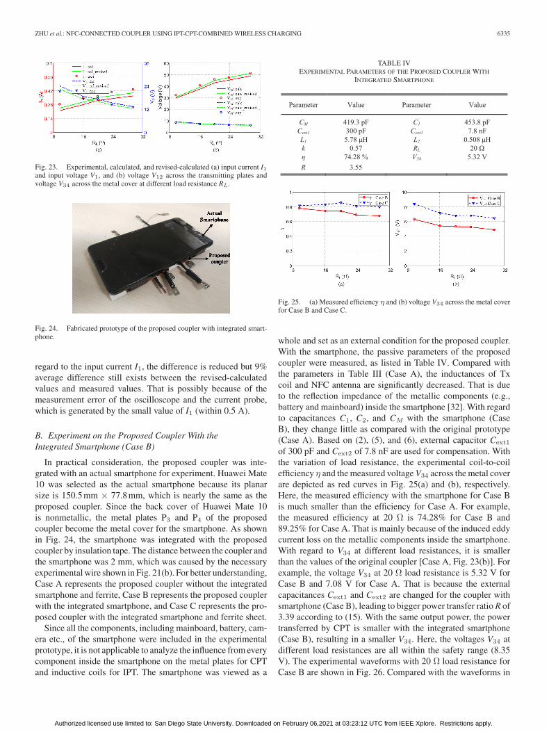
To conduct the experiment for the proposed NFC-connectedcoupler, an AG 1016 power amplifier from T&C Power wasutilized to provide the 2.5-MHz ac waveform. After integrat-ing the proposed coupler with the power amplifier and loadresistance of 20 Ω, 5.6 W output power was achieved with89.3% coil-to-coil efficiency. The corresponding experimentalwaveforms and test results are shown in Fig. 22 and Table III,respectively. It is noteworthy that the scales of the waveforms aredenoted with labels and marked by dotted circles. Here, the inputvoltage V1 was nearly in phase with the input current I1 and thephase difference between the input current and output currentwas 96.3° (107 ns at 2.5 MHz). With 5.6 W output power, thevoltage V34 across the metal cover was measured to be 7.08 V,which met the safety requirement (8.35 V). It is noteworthy thatthe measured PIPT was calculated by ωM |I1I3| sin θI and themeasured PCPT was calculated by ωCM |V12V34| sin θV , whereθI indicates the phase difference between I1 and I3 and θVrepresents the phase difference between V12 and V34. In thiscase, 4.36 W power was transferred by magnetic field and 1.75W power was transferred by electric field.
With a fixed output power, the load resistance is varied toverify the circuit characteristic of the proposed coupler. InFig. 23, the experimental input voltage V1 and voltage V34 acrossthe metal cover correspond well with the calculated values.However, noticeable difference exists between the calculatedvalues and experimental values for input current I1 and volt-age V12. Since the inductance L2 of the NFC antenna is verysmall (0.77 μH), measurement of L2 may be inaccurate. Ifthe inductance of the NFC antenna decreases to 0.63 μH, therevised-calculated results are plotted in Fig. 23 as green curvesfor comparison. As shown in Fig. 23, nearly no difference existsbetween the revised-calculated V12 and the measured V12. With
Authorized licensed use limited to: San Diego State University. Downloaded on February 06,2021 at 03:23:12 UTC from IEEE Xplore. Restrictions apply.
ZHU et al.: NFC-CONNECTED COUPLER USING IPT-CPT-COMBINED WIRELESS CHARGING 6335
Fig. 23. Experimental, calculated, and revised-calculated (a) input current I1and input voltage V1, and (b) voltage V12 across the transmitting plates andvoltage V34 across the metal cover at different load resistance RL.
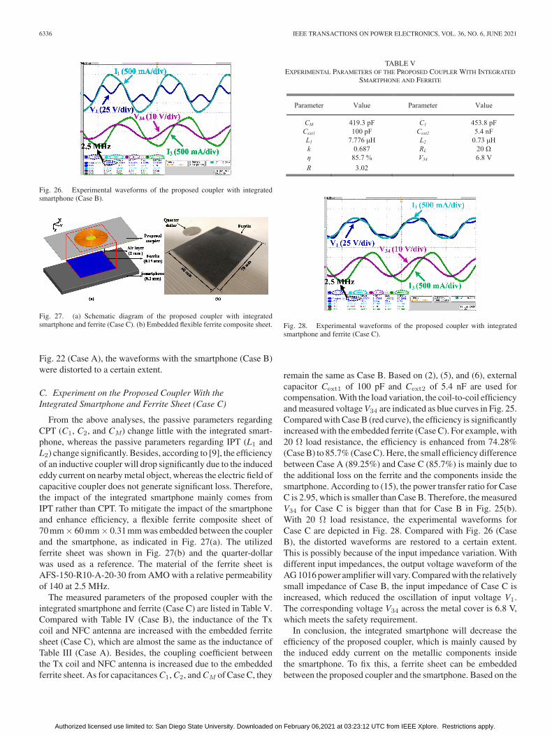
Fig. 24. Fabricated prototype of the proposed coupler with integrated smart-phone.
regard to the input current I1, the difference is reduced but 9%average difference still exists between the revised-calculatedvalues and measured values. That is possibly because of themeasurement error of the oscilloscope and the current probe,which is generated by the small value of I1 (within 0.5 A).
B. Experiment on the Proposed Coupler With theIntegrated Smartphone (Case B)
In practical consideration, the proposed coupler was inte-grated with an actual smartphone for experiment. Huawei Mate10 was selected as the actual smartphone because its planarsize is 150.5 mm × 77.8 mm, which is nearly the same as theproposed coupler. Since the back cover of Huawei Mate 10is nonmetallic, the metal plates P3 and P4 of the proposedcoupler become the metal cover for the smartphone. As shownin Fig. 24, the smartphone was integrated with the proposedcoupler by insulation tape. The distance between the coupler andthe smartphone was 2 mm, which was caused by the necessaryexperimental wire shown in Fig. 21(b). For better understanding,Case A represents the proposed coupler without the integratedsmartphone and ferrite, Case B represents the proposed couplerwith the integrated smartphone, and Case C represents the pro-posed coupler with the integrated smartphone and ferrite sheet.
Since all the components, including mainboard, battery, cam-era etc., of the smartphone were included in the experimentalprototype, it is not applicable to analyze the influence from everycomponent inside the smartphone on the metal plates for CPTand inductive coils for IPT. The smartphone was viewed as a
TABLE IVEXPERIMENTAL PARAMETERS OF THE PROPOSED COUPLER WITH
INTEGRATED SMARTPHONE
Fig. 25. (a) Measured efficiency η and (b) voltage V34 across the metal coverfor Case B and Case C.
whole and set as an external condition for the proposed coupler.With the smartphone, the passive parameters of the proposedcoupler were measured, as listed in Table IV. Compared withthe parameters in Table III (Case A), the inductances of Txcoil and NFC antenna are significantly decreased. That is dueto the reflection impedance of the metallic components (e.g.,battery and mainboard) inside the smartphone [32]. With regardto capacitances C1, C2, and CM with the smartphone (CaseB), they change little as compared with the original prototype(Case A). Based on (2), (5), and (6), external capacitor Cext1
of 300 pF and Cext2 of 7.8 nF are used for compensation. Withthe variation of load resistance, the experimental coil-to-coilefficiency η and the measured voltage V34 across the metal coverare depicted as red curves in Fig. 25(a) and (b), respectively.Here, the measured efficiency with the smartphone for Case Bis much smaller than the efficiency for Case A. For example,the measured efficiency at 20 Ω is 74.28% for Case B and89.25% for Case A. That is mainly because of the induced eddycurrent loss on the metallic components inside the smartphone.With regard to V34 at different load resistances, it is smallerthan the values of the original coupler [Case A, Fig. 23(b)]. Forexample, the voltage V34 at 20 Ω load resistance is 5.32 V forCase B and 7.08 V for Case A. That is because the externalcapacitances Cext1 and Cext2 are changed for the coupler withsmartphone (Case B), leading to bigger power transfer ratio R of3.39 according to (15). With the same output power, the powertransferred by CPT is smaller with the integrated smartphone(Case B), resulting in a smaller V34. Here, the voltages V34 atdifferent load resistances are all within the safety range (8.35V). The experimental waveforms with 20 Ω load resistance forCase B are shown in Fig. 26. Compared with the waveforms in
Authorized licensed use limited to: San Diego State University. Downloaded on February 06,2021 at 03:23:12 UTC from IEEE Xplore. Restrictions apply.
6336 IEEE TRANSACTIONS ON POWER ELECTRONICS, VOL. 36, NO. 6, JUNE 2021
Fig. 26. Experimental waveforms of the proposed coupler with integratedsmartphone (Case B).
Fig. 27. (a) Schematic diagram of the proposed coupler with integratedsmartphone and ferrite (Case C). (b) Embedded flexible ferrite composite sheet.
Fig. 22 (Case A), the waveforms with the smartphone (Case B)were distorted to a certain extent.
C. Experiment on the Proposed Coupler With theIntegrated Smartphone and Ferrite Sheet (Case C)
From the above analyses, the passive parameters regardingCPT (C1, C2, and CM) change little with the integrated smart-phone, whereas the passive parameters regarding IPT (L1 andL2) change significantly. Besides, according to [9], the efficiencyof an inductive coupler will drop significantly due to the inducededdy current on nearby metal object, whereas the electric field ofcapacitive coupler does not generate significant loss. Therefore,the impact of the integrated smartphone mainly comes fromIPT rather than CPT. To mitigate the impact of the smartphoneand enhance efficiency, a flexible ferrite composite sheet of70 mm× 60 mm× 0.31 mm was embedded between the couplerand the smartphone, as indicated in Fig. 27(a). The utilizedferrite sheet was shown in Fig. 27(b) and the quarter-dollarwas used as a reference. The material of the ferrite sheet isAFS-150-R10-A-20-30 from AMO with a relative permeabilityof 140 at 2.5 MHz.
The measured parameters of the proposed coupler with theintegrated smartphone and ferrite (Case C) are listed in Table V.Compared with Table IV (Case B), the inductance of the Txcoil and NFC antenna are increased with the embedded ferritesheet (Case C), which are almost the same as the inductance ofTable III (Case A). Besides, the coupling coefficient betweenthe Tx coil and NFC antenna is increased due to the embeddedferrite sheet. As for capacitances C1, C2, and CM of Case C, they
TABLE VEXPERIMENTAL PARAMETERS OF THE PROPOSED COUPLER WITH INTEGRATED
SMARTPHONE AND FERRITE
Fig. 28. Experimental waveforms of the proposed coupler with integratedsmartphone and ferrite (Case C).
remain the same as Case B. Based on (2), (5), and (6), externalcapacitor Cext1 of 100 pF and Cext2 of 5.4 nF are used forcompensation. With the load variation, the coil-to-coil efficiencyand measured voltage V34 are indicated as blue curves in Fig. 25.Compared with Case B (red curve), the efficiency is significantlyincreased with the embedded ferrite (Case C). For example, with20 Ω load resistance, the efficiency is enhanced from 74.28%(Case B) to 85.7% (Case C). Here, the small efficiency differencebetween Case A (89.25%) and Case C (85.7%) is mainly due tothe additional loss on the ferrite and the components inside thesmartphone. According to (15), the power transfer ratio for CaseC is 2.95, which is smaller than Case B. Therefore, the measuredV34 for Case C is bigger than that for Case B in Fig. 25(b).With 20 Ω load resistance, the experimental waveforms forCase C are depicted in Fig. 28. Compared with Fig. 26 (CaseB), the distorted waveforms are restored to a certain extent.This is possibly because of the input impedance variation. Withdifferent input impedances, the output voltage waveform of theAG 1016 power amplifier will vary. Compared with the relativelysmall impedance of Case B, the input impedance of Case C isincreased, which reduced the oscillation of input voltage V1.The corresponding voltage V34 across the metal cover is 6.8 V,which meets the safety requirement.
In conclusion, the integrated smartphone will decrease theefficiency of the proposed coupler, which is mainly caused bythe induced eddy current on the metallic components insidethe smartphone. To fix this, a ferrite sheet can be embeddedbetween the proposed coupler and the smartphone. Based on the
Authorized licensed use limited to: San Diego State University. Downloaded on February 06,2021 at 03:23:12 UTC from IEEE Xplore. Restrictions apply.

ZHU et al.: NFC-CONNECTED COUPLER USING IPT-CPT-COMBINED WIRELESS CHARGING 6337
analyses above, the proposed coupler can be applied to practicalsmartphone applications.
VII. CONCLUSION
In this article, an NFC-CPT-connected coupler applying IPT-CPT-combined wireless charging is proposed for metal-coversmartphones. By converting the metal cover from a metal barrierto receiving plates, CPT through the metal cover is achieved. Byconnecting the inductive coils to the metal plates, the inductivecoils perform as compensation inductance and power transfercoils simultaneously, thus realizing a combined IPT-CPT. Sincethe already-existing metal cover of 150 mm × 75 mm and NFCantenna of 30 mm × 22 mm are utilized to construct the receiverof the proposed coupler, only a parallel capacitor of 5 nF isintegrated inside the smartphone, which greatly saves space andcost inside the smartphone. The power transfer ratio is set byadjusting the two external parallel capacitors Cext1 and Cext2
to be 100 pF and 5 nF, respectively. At 2.5 MHz operatingfrequency, 4.36 W inductive power and 1.75 W capacitive powerare transferred with 89.25% coil-to-coil efficiency. With 5.6 Woutput power, the voltage across the metal cover is 7.08 V, whichmeets the safety voltage requirement at HF. By embedding aferrite sheet, the proposed coupler can achieve 85.7% coil-to-coil efficiency and 5.32 V voltage across the metal cover withan actual smartphone attached. Considering space, cost, eddycurrent loss, and safety, the proposed NFC-connected coupler isa good candidate for metal-cover smartphone applications.
REFERENCES
[1] S. Li and C. C. Mi, “Wireless power transfer for electric vehicle appli-cations,” IEEE Trans. Emerg. Sel. Topics Power Electron., vol. 3, no. 1,pp. 4–17, Mar. 2015.
[2] S. Y. Hui, “Planar wireless charging technology for portable electronicproducts and Qi,” Proc. IEEE, vol. 101, no. 6, pp. 1290–1301, Jun. 2013.
[3] “The Qi wireless power transfer system power class 0 specification, parts1 and 2: Interface definitions, ver. 1.2.3,” Wireless Power Consortium,Feb. 2017. [Online]. Available: https://www.wirelesspowerconsortium.com/data/downloadables/2/2/0/5/qi-wireless-power-specification-non-confidential.zip
[4] Y. Jang and M. Jovanovic, “A contactless electrical energy transmissionsystem for portable-telephone battery chargers,” IEEE Trans. Ind. Elec-tron., vol. 50, no. 3, pp. 520–527, Jun. 2003.
[5] C.-G. Kim, D.-H. Seo, J.-S. You, J.-H. Park, and B. H. Cho, “Design of acontactless battery charger for cellular phone,” IEEE Trans. Ind. Electron.,vol. 48, no. 6, pp. 1238–1247, Dec. 2001.
[6] D. J. Graham, J. A. Neasham, and B. S. Sharif, “Investigation of methodsfor data communication and power delivery through metals,” IEEE Trans.Ind. Electron., vol. 58, no. 10, pp. 4972–4980, Oct. 2011.
[7] O. Imoru, A. Jassal, H. Polinder, E. Nieuwkoop, J. Tsado, and A. A. Jimoh,“An inductive power transfer through metal object,” in Proc. 1st Int. FutureEnergy Electron. Conf., Nov. 2013, pp. 246–251.
[8] J. Dai and D. Ludois, “A survey of wireless power transfer and a criticalcomparison of inductive and capacitive coupling for small gap appli-cations,” IEEE Trans. Power Electron., vol. 30, no. 11, pp. 6017–6029,Nov. 2015.
[9] F. Lu, H. Zhang, H. Hofmann, and C. Mi, “A double-sided LCLC-compensated capacitive power transfer system for electric vehicle charg-ing,” IEEE Trans. Power Electron., vol. 30, no. 11, pp. 6011–6014,Nov. 2015.
[10] H. Zhang, F. Lu, H. Hofmann, W. Liu, and C. Mi, “A four-plate compactcapacitive coupler design and LCL-compensated topology for capacitivepower transfer in electric vehicle charging application,” IEEE Trans. PowerElectron., vol. 31, no. 12, pp. 8541–8551, Dec. 2016.
[11] IEEE Standard for Safety Levels With Respect to Human Exposure toRadio Frequency Electromagnetic Fields, 3kHz to 300 GHz, IEEE StdC95.1, 2005.
[12] Method of Measurement of Touch Current and Protective ConductorCurrent, IEC 60990, 1999.
[13] F. Lu, H. Zhang, and C. Mi, “A two-plate capacitive wireless power transfersystem for electric vehicle charging applications,” IEEE Trans. PowerElectron., vol. 33, no. 2, pp. 964–969, Feb. 2018.
[14] Y. Zhang, T. Kan, Z. Yan, Y. Mao, Z. Wu, and C. Mi, “Modeling andanalysis of series-none compensation for wireless power transfer systemswith a strong coupling,” IEEE Trans. Power Electron., vol. 34, no. 2,pp. 1209–1215, Feb. 2019.
[15] J. Kim, D. Kim, and Y. Park, “Analysis of capacitive impedance matchingnetwork for simultaneous wireless power transfer to multiple devices,”IEEE Trans. Ind. Electron., vol. 62, no. 5, pp. 2807–2813, May 2015.
[16] S. Li, W. Li, J. Deng, T. D. Nguyen, and C. Mi, “A double-sided LCCcompensation network and its tuning method for wireless power transfer,”IEEE Trans. Veh. Technol., vol. 64, no. 6, pp. 2261–2273, Jun. 2015.
[17] J. Dai and D. C. Ludois, “Biologically inspired coupling pixilation forposition independence in capacitive power transfer surfaces,” in Proc.IEEE Appl. Power Electron. Conf. Expo., 2015, pp. 3276–3282.
[18] L. Chao, A. P. Hu, G. A. Covic, and N. C. Nair, “Comparative study ofCCPT systems with two different inductor tuning positions,” IEEE Trans.Power Electron., vol. 27, pp. 294–306, Jan. 2012.
[19] F. Lu, H. Zhang, H. Hofmann, and C. C. Mi, “A double-sided LC-Compensation circuit for loosely coupled capacitive power transfer,” IEEETrans. Power Electron., vol. 33, no. 2, pp. 1633–1643, Feb. 2018.
[20] D. Vincent, P. S. Huynh, N. A. Azeez, L. Patnaik, and S. S. Williamson,“Evolution of hybrid inductive and capacitive AC links for wireless EVCharging—A comparative overview,” IEEE Trans. Transport. Electrific.,vol. 5, no. 4, pp. 1060–1077, Dec. 2019.
[21] F. Lu, H. Zhang, H. Health, and C. C. Mi, “An inductive and capac-itive combined wireless power transfer system with LC-compensatedtopology,” IEEE Trans. Power Electron., vol. 31, no. 12, pp. 8471–8482,Dec. 2016.
[22] B. Luo, T. Long, R. Mai, R. Dai, Z. He, and W. Li, “Analysis anddesign of hybrid inductive and capacitive wireless power transfer for high-power applications,” IET Power Electron., vol. 11, no. 14, pp. 2263–2270,Nov. 2018.
[23] F. Lu, H. Zhang, H. Hofmann, and C. C. Mi, “An inductive and capacitiveintegrated coupler and its LCL compensation circuit design for wirelesspower transfer,” IEEE Trans. Ind. Appl., vol. 53, no. 5, pp. 4903–4913,Sep./Oct. 2017.
[24] B. Luo, T. Long, L. Guo, R. Dai, R. Mai, and Z. He, “Analysis and designof inductive and capacitive hybrid wireless power transfer system forrailway application,” IEEE Trans. Ind. Appl., vol. 56, no. 3, pp. 3034–3042,May/Jun. 2020.
[25] X. Li, C. Tang, X. Dai, P. Deng, and Y. Su, “An inductive and capacitivecombined parallel transmission of power and data for wireless power trans-fer systems,” IEEE Trans. Power Electron., vol. 33, no. 6, pp. 4980–4991,Jun. 2018.
[26] Y. Su, W. Zhou, A. P. Hu, C. Tang, S. Xie, and Y. Sun, “Full-duplex com-munication on the shared channel of a capacitively coupled power transfersystem,” IEEE Trans. Power Electron., vol. 32, no. 4, pp. 3229–3239,Apr. 2017.
[27] X. Y. Zhang, C.-D. Xue, and J.-K. Lin, “Distance-insensitive wirelesspower transfer using mixed electric and magnetic coupling for frequencysplitting suppression,” IEEE Trans. Microw. Theory Techn., vol. 65, no.11, pp. 4307–4316, Nov. 2017.
[28] W. Zhou, Y.-G. Su, L. Huang, X.-D. Qing, and A. P. Hu, “Wirelesspower transfer across a metal barrier by combined capacitive and inductivecoupling,” IEEE Trans. Ind. Electron., vol. 66, no. 5, pp. 4031–4041,May 2019.
[29] J. Q. Zhu, Y. L. Ban, R. M. Xu, and C. C. Mi, “An NFC-CPT-combinedcoupler with series-none compensation for metal-cover smartphone appli-cations,” IEEE J. Emerg. Sel. Topics Power Electron., early access, Jun.16, 2020, doi: 10.1109/JESTPE.2020.3002858.
[30] J. Fischer, “NFC in cell phones: The new paradigm for an interactiveworld,” IEEE Commun. Mag., vol. 47, no. 6, pp. 22–28, Jun. 2009.
[31] Z. Yan et al., “Frequency optimization of a loosely coupled underwaterwireless power transfer system considering eddy current loss,” IEEE Trans.Ind. Electron., vol. 66, no. 5, pp. 3468–3476, May 2019.
[32] Y. Zhang, T. Lu, Z. Zhao, F. He, K. Chen, and L. Yuan, “Selective wirelesspower transfer to multiple loads using receivers of different resonantfrequencies,” IEEE Trans. Power Electron., vol. 30, no. 11, pp. 6001–6005,Nov. 2015.
Authorized licensed use limited to: San Diego State University. Downloaded on February 06,2021 at 03:23:12 UTC from IEEE Xplore. Restrictions apply.

6338 IEEE TRANSACTIONS ON POWER ELECTRONICS, VOL. 36, NO. 6, JUNE 2021
Jia-Qi Zhu was born in Henan, China, in 1992. Hereceived the B.S. degree in electronic informationscience and technology from the Southwest JiaotongUniversity (SWJTU), Chengdu, China, in 2014. He iscurrently working toward the Ph.D. degree with theUniversity of Electronic Science and Technology ofChina (UESTC), Chengdu, China.
In 2018, he received funding from UESTC andChina Scholarship Council, and became a Joint Ph.D.Student with the Department of Electrical and Com-puter Engineering, San Diego State University, San
Diego, CA, USA. His main research interests include near-field communication(NFC) and wireless power transfer (WPT) antennas for smartphone applications,especially near field antennas operating with metal-cover smartphones.
Yong-Ling Ban was born in Henan, China. He re-ceived the B.S. degree in mathematics from ShandongUniversity, Jinan, China, in 2000, the M.S. degreein electromagnetics from Peking University, Beijing,China, in 2003, and the Ph.D. degree in microwaveengineering from the University of Electronic Scienceand Technology of China (UESTC), Chengdu, China,in 2006, respectively.
In July 2006, he joined the Xi’an Mechanical andElectric Information Institute, Xi’an, China, as a Mi-crowave Engineer. He then joined Huawei Technolo-
gies Co., Ltd., Shenzhen, China, where he designed and implemented variousterminal antennas for 15 data card and mobile phone products customized fromleading telecommunication industries such as Vodafone. From September 2010to July 2016, he was an Associate Professor with UESTC, where he is currentlya Professor. From May 2014 to April 2015, he visited Queen Mary University ofLondon, as a Scholar Visitor. He is the author of more than 60 referred journaland conference papers on his research topics and holds 20 granted and pendingChinese and overseas patents. His research interests include wideband smallantennas for 4G/5G handset devices, MIMO antennas, and millimeter waveantenna arrays.
Rui-Min Xu (Member, IEEE) was born in Sichuan,China, in 1958. He received the B.S. and Ph.D. de-grees in electromagnetic field and microwave tech-niques from the University of Electronic Science andTechnology of China (UESTC), Chengdu, China, in1982 and 2007, respectively.
He is currently a Full Professor with UESTC.His current research interests include microwave andmillimeter-wave technologies and applications, andradar systems.
Chunting Chris Mi (Fellow, IEEE) received theB.S.E.E. and M.S.E.E. degrees from the Northwest-ern Polytechnical University, Xi’an, China, in 1985and 1988, respectively, and the Ph.D. degree from theUniversity of Toronto, Toronto, ON, Canada, in 2001,all in electrical engineering.
He is currently a Professor and Chair of Electri-cal and Computer Engineering and the Director ofthe Department of Energy (DOE)-funded GraduateAutomotive Technology Education (GATE) Centerfor Electric Drive Transportation, San Diego State
University (SDSU), San Diego, CA, USA. Prior to joining SDSU, he was withUniversity of Michigan-Dearborn, Dearborn, MI, USA, from 2001 to 2015.
Authorized licensed use limited to: San Diego State University. Downloaded on February 06,2021 at 03:23:12 UTC from IEEE Xplore. Restrictions apply.