an asm international publication heattreating … · stamping dies are cast from all of the...
TRANSCRIPT

HEATTREATINGPROGRESSTHE BUSINESS AND TECHNOLOGY OF HEAT TREATING
An ASM International®
Publication
TM
SM
www.asminternational.org SEPTEMBER/OCTOBER 2006
PLASMA NITRIDING
LARGESTAMPING DIES
PLASMA NITRIDING
LARGESTAMPING DIES
ATMOSPHERESAFETY
MODELING AND SIMULATION
0906COVER.qxp 9/28/2006 10:06 AM Page 1

Plasma nitriding offers away to significantly improve the surface
properties of tool steelstamping dies, and is notlimited by their size to itsapplication, as are some
alternative surface treatments.
E. Rolin’ski** G. Sharp
Advanced Heat Treat Corp.Monroe, Mich.
and A. Konieczny*
U.S. SteelTroy, Mich.
** Member of ASM International andmember, ASM Heat Treating Society
* Member ASM International
A dvanced high-strengthsteels (AHSS), such as dualphase (DP), transformation-induced plasticity (TRIP),
and some other high-strength steels(HSS) for auto body parts require theuse of stamping dies having im-proved durability and wear resist-ance [1-5]. In addition, most of thesenew automotive steels also are coatedwith a zinc or iron-zinc alloy galva-nized coating before stamping, whichgreatly affects the coefficient of fric-tion during stamping [3]. AHSS alsohave a higher volume fraction of veryhard martensite, which requires im-proved tool surface finish.
Stamping of these materials is ac-companied by higher contact pres-sures between the tool and stampedmaterial and higher tool temperaturefrom frictional heat, which places ad-ditional requirements on tool surfaceengineering to prevent powdering,galling, and other damage to the gal-vanized coating [6]. It is important toprevent damage to the coating to en-sure the quality of stamped partswhen Class Asurface is required and
to lower die maintenance costs. Galvanically applied hard chrom-
ium, which has been extensivelyused to coat stamping dies, cannotwithstand some of the high contactstresses generated during stampingand forming AHSS. A combinationof various surface treatments (i.e.,duplex surface engineering) allowsproducing a surface compositehaving a combination of propertiesunobtainable through any indi-vidual surface technology. For ex-ample, combining induction orflame hardening with consecutivegas or plasma nitriding treatmentsand coating with a hard PVD layercan produce a superior tool capableof withstanding the most difficultstamping applications [7]. For largetools where size limits the applica-tion of a hard PVD layer, coated in-serts or welded draw beads can beused [8]. Other existing surface en-gineering techniques can provideduplex diffusion and coating layers,and often are used to treat smallstamping dies. More demandingapplications can require the forma-tion of even more complex duplexdiffusion and coating layers, suchas with plasma nitriding, to with-stand severe contact stress appliedto the tool [9].
While there are many differentcombinations of surface treatmentsthat can be applied to stamping dies,a critical limiting factor in the abilityto apply a specific treatment is theunavailability of surface engineeringchambers large enough to accommo-date the work, a limitation that doesnot apply to plasma nitriding tech-nology. Plasma (ion) nitriding aloneis recognized as a prime hardeningtreatment of the larger size stampingdies [8, 10]. Figure 1 shows examples ofsuch large dies plasma nitrided atthe Advanced Heat Treat Corp.Monroe, Mich., facility.
For nitrided dies used to producestampings having a Class A surface,
PLASMA NITRIDINGAUTOMOTIVE STAMPING DIES
View of a 19,000 lb stamping binder undergoing plasma nitriding in the vacuum chamber.
Plasma.qxp 9/28/2006 10:07 AM Page 1
the lowest possible tool surface roughness and asmooth tool-hardness gra-dient across the nitridedlayer are recommended. Lowsurface roughness comparableto chrome plating can beachieved by subsequent pol-ishing of the ion-nitrided toolsurface.
Many die materials, such asthose listed in Table 1, havechemical compositions thatmake them good candidatesfor plasma nitriding. Full sizestamping dies are cast from allof the materials in Table 1 except M2 high-speed tool steel, which isused for inserts and welded beads,especially in the most stressed areaof the stamping tools.
Importance of Proper Processingand Die Finishing
Plasma nitriding of large tools re-quires a good starting vacuum andclean chamber atmosphere to pro-duce a proper case structure havingmaximum hardness (with or withouta nonporous compound zone of lim-ited thickness). This cannot beachieved without proper cleaning ofdies before loading them to the ni-triding chamber. The most commonimpurities that must be removed arelubricants adsorbed on the die sur-face during tryouts and paint in thecase of processing repaired dies.These impurities contaminate thevacuum system and result in dopingof the plasma; that is, they increasethe nitriding potential of the plasmaresulting in formation of the un-wanted case structure having aporous ε (epsilon) plus γ′ (gamma
prime) compoundzone, or they drasti-cally reduce the ki-netics of nitridingwhen too muchoxygen-bearing gasesare present [11].
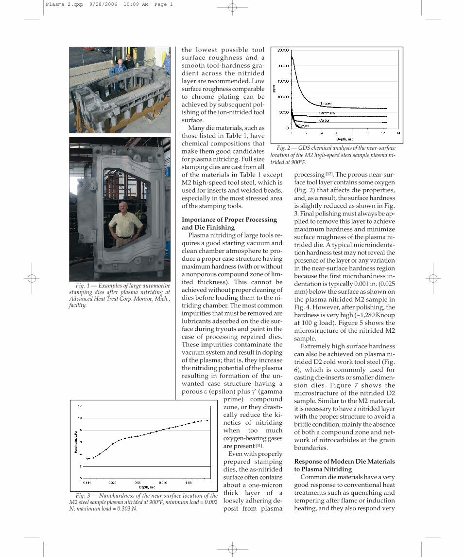
Even with properlyprepared stampingdies, the as-nitridedsurface often containsabout a one-micronthick layer of aloosely adhering de-posit from plasma
processing [12]. The porous near-sur-face tool layer contains some oxygen(Fig. 2) that affects die properties,and, as a result, the surface hardnessis slightly reduced as shown in Fig.3. Final polishing must always be ap-plied to remove this layer to achievemaximum hardness and minimizesurface roughness of the plasma ni-trided die. A typical microindenta-tion hardness test may not reveal thepresence of the layer or any variationin the near-surface hardness regionbecause the first microhardness in-dentation is typically 0.001 in. (0.025mm) below the surface as shown onthe plasma nitrided M2 sample inFig. 4. However, after polishing, thehardness is very high (~1,280 Knoopat 100 g load). Figure 5 shows the microstructure of the nitrided M2sample.
Extremely high surface hardnesscan also be achieved on plasma ni-trided D2 cold work tool steel (Fig.6), which is commonly used forcasting die-inserts or smaller dimen-sion dies. Figure 7 shows the microstructure of the nitrided D2sample. Similar to the M2 material,it is necessary to have a nitrided layerwith the proper structure to avoid abrittle condition; mainly the absenceof both a compound zone and net-work of nitrocarbides at the grainboundaries.
Response of Modern Die Materialsto Plasma Nitriding
Common die materials have a verygood response to conventional heattreatments such as quenching andtempering after flame or inductionheating, and they also respond very
Fig. 1 — Examples of large automotivestamping dies after plasma nitriding at Advanced Heat Treat Corp. Monroe, Mich., facility.
Fig. 2 — GDS chemical analysis of the near-surfacelocation of the M2 high-speed steel sample plasma ni-trided at 900ºF.
Fig. 3 — Nanohardness of the near surface location of the M2 steel sample plasma nitrided at 900ºF; minimum load = 0.002N; maximum load = 0.303 N.
Plasma 2.qxp 9/28/2006 10:09 AM Page 1

well to plasma nitriding (Table 2).Surface hardness after nitriding isvery high (over 90 HR15N) for all thetested materials except Carmo, whichformed the lowest case depth andhad low core hardness due to its an-nealed condition. The other materialsformed a sufficiently deep case to re-sist indentation of the Rockwell hard-ness indenter under the 15 kg load,
or they had high core hardness (suchas with M2, which has good resist-ance to tempering at nitriding tem-peratures). Superficial hardnessmeasurements taken using a portableVickers instrument ranged above 850HV1 (more than 65 HRC equivalent).Photomicrographs of the plasma ni-trided samples tested with corre-sponding hardness profiles are
Table 1 — Nominal chemical composition of die materials evaluated Chemical composition, wt%
Material C Mn Si S Cr Ni Cu Al Mo V W
M2 0.85 0.35 0.35 0.03 4.25 — — — 5.00 2.00 6.00
D2 1.5 0.6 0.6 — 12 0.3 — — 0.95 1.1 —
Cast Cut# 1 0.60 1.45 0.60 0.12 1.50 0.25 0.40 0.10 — — —
Caldie 0.7 0.5 0.2 — 5.0 — — — 2.3 0.5 —
Carmo 0.6 0.8 0.35 — 4.5 — — — 0.5 0.2 —
M2 is a high-speed tool steel. D2 is a cold-work tool steel. Cast Cut#1 is a resistered trademark of Nelson & Assoc. Research Inc., Clinton Township, Mich. Caldieand Carmo are trademarks of Böhler Uddeholm Corp, Rolling Hills, Ill.
Table 2 — Average hardness of nitrided and quenched and tempered die materials Nitrided 950oF/15 h Nitrided 900oF/15 h
Quenched in 25% N2-75% H2 in 5% N2-95% H2 and temperedMaterial Surface, HR15N Surface, HV1 Surface, HR15N Surface, HV1 HRC
M2 — — 94.5 1080 64-66
D2 — — 92.8 1000 61-64
Cast Cut# 1 91.1 874 91.5 878 60-62
Caldie 92.9 880 90.1 855 61-62
Carmo 90.0 930 83.0 850 63-65
50µm
Fig. 4 — Hardness profile in the M2 sample plasma nitrided at900ºF; total case depth is 0.0036 in.
Fig. 6 — Hardness profile in the D2 sample plasma nitrided at 900ºF.Total case depth 0.004 in.
Fig. 7 — Photo-micrograph of the D2 sample plasmanitrided at 900ºFshowing the com-pound zone-free andnetwork-free struc-ture of the nitridedlayer. Etchant: 2%nital.
Fig. 5 — Photo-micrograph of the
M2 sample plasma nitrided at 900ºFshowing the com-
pound zone-free andnetwork-free struc-ture of the nitridedlayer. Etchant: 2% 50µm
Plasma 2.qxp 9/28/2006 10:09 AM Page 3
50µm
Fig. 8 — Photo-micrograph of the CastCut#1 sample plasma
nitrided at 950ºFshowing the com-
pound zone at the sur-face and normalizedstructure of the steel in the nitrided layer.
Etchant: 2% nital.
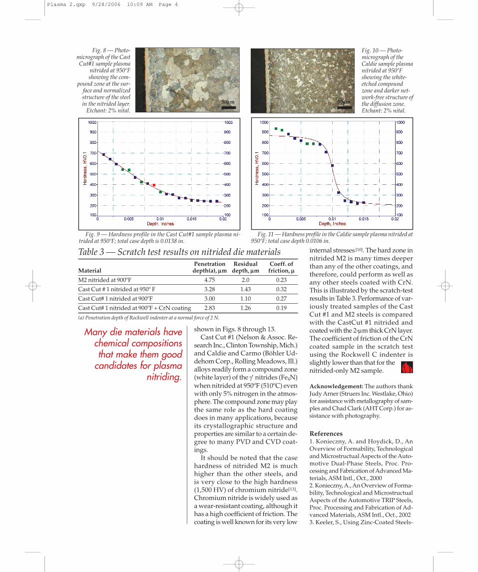
Fig. 10 — Photo-micrograph of theCaldie sample plasmanitrided at 950ºFshowing the white-etched compoundzone and darker net-work-free structure ofthe diffusion zone.Etchant: 2% nital.
50µm
Fig. 9 — Hardness profile in the Cast Cut#1 sample plasma ni-trided at 950ºF; total case depth is 0.0138 in.
Fig. 11 — Hardness profile in the Caldie sample plasma nitrided at950ºF; total case depth 0.0106 in.
shown in Figs. 8 through 13.Cast Cut #1 (Nelson & Assoc. Re-
search Inc., Clinton Township, Mich.)and Caldie and Carmo (Böhler Ud-dehom Corp., Rolling Meadows, Ill.)alloys readily form a compound zone(white layer) of the γ′ nitrides (Fe4N)when nitrided at 950oF (510oC) evenwith only 5% nitrogen in the atmos-phere. The compound zone may playthe same role as the hard coatingdoes in many applications, becauseits crystallographic structure andproperties are similar to a certain de-gree to many PVD and CVD coat-ings.
It should be noted that the casehardness of nitrided M2 is muchhigher than the other steels, and is very close to the high hardness(1,500 HV) of chromium nitride[13].Chromium nitride is widely used asa wear-resistant coating, although ithas a high coefficient of friction. Thecoating is well known for its very low
internal stresses [10]. The hard zone innitrided M2 is many times deeperthan any of the other coatings, andtherefore, could perform as well asany other steels coated with CrN.This is illustrated by the scratch-testresults in Table 3. Performance of var-iously treated samples of the CastCut #1 and M2 steels is comparedwith the CastCut #1 nitrided andcoated with the 2-µm thick CrN layer.The coefficient of friction of the CrNcoated sample in the scratch testusing the Rockwell C indenter isslightly lower than that for thenitrided-only M2 sample.
Acknowledgement: The authors thankJudy Arner (Struers Inc. Westlake, Ohio)for assistance with metallography of sam-ples and Chad Clark (AHT Corp.) for as-sistance with photography.
References1. Konieczny, A. and Hoydick, D., AnOverview of Formability, Technologicaland Microstructual Aspects of the Auto-motive Dual-Phase Steels, Proc. Pro-cessing and Fabrication of Advanced Ma-terials, ASM Intl., Oct., 20002. Konieczny, A., An Overview of Forma-bility, Technological and MicrostructualAspects of the Automotive TRIP Steels,Proc. Processing and Fabrication of Ad-vanced Materials, ASM Intl., Oct., 20023. Keeler, S., Using Zinc-Coated Steels-
Table 3 — Scratch test results on nitrided die materialsPenetration Residual Coeff. of
Material depth(a), µm depth, µm friction, µ
M2 nitrided at 900ºF 4.75 2.0 0.23
Cast Cut # 1 nitrided at 950º F 3.28 1.43 0.32
Cast Cut# 1 nitrided at 900ºF 3.00 1.10 0.27
Cast Cut# 1 nitrided at 900ºF + CrN coating 2.83 1.26 0.19
(a) Penetration depth of Rockwell indenter at a normal force of 2 N.
Many die materials havechemical compositionsthat make them good
candidates for plasmanitriding.
Plasma 2.qxp 9/28/2006 10:09 AM Page 4

Friction Change?, Metal Forming, Feb. p 72, 20014. Kuvin, K., Ford’s New DP 600 Die Standards, Metal Forming,Feb. p 20, 20065. Baron, J. and Shaw, J., Forming AHSS, Metal Forming, Feb., p24, 20016. Shih, M., Temperature Effects on Draw Bead Friction for Ad-vanced High-Strength Steels, Great Design in Steel 2006 Sem-inar, www.steel.org.7. Nelson, J., Thermally Treating Tool Steels and Alloy Steels,Nelson & Assoc. Research, Inc.8. Rembges, W., Putting PN & PNC into Production, Ht. Trtg.,p 20, 19939. Sun, Y, and Bell, T., Combined plasma nitriding and PVD treat-ments, Trans. Inst. of Metal Finishing, Vol. 70, p 38, 1992 10. Hurkmans, T., et al., Perspectives for Replacement of HardChrome by PVD, Proc., 2nd Tech. Conf., Soc. Vac. Coaters, p 364,199911. Ruset, C., et al., An Investigation of the Gas Compositionduring Plasma Thermochemical Treatments, Ht. Trtmnt. of Metals,No 4, p 90, 199412. Rolin’ski, E. and Sharp, G., Negative Effect of the ReactiveSputtering in an Industrial Plasma Nitriding, J. Matls. Engrg.&Perf., Vol. 14, June, p 243, 200513. Kawate, M, et al., Microhardness and lattice parameter ofCr1-xAlxN films, J. Vac. Sc. Tech., A 20(2), Mar./Apr. p 569, 2002
For more information: Dr. Eng. Edward A. Rolin’ski is Vice Pres-ident Technology, Advanced Heat Treat Corp. 1625 Rose St.,Monroe, MI 48162; tel: 734-243-0063; fax: 734-243-4066; E-mail:[email protected]; Internet: www.ahtweb.com.
Fig.12 — Photo-micrograph of the Carmo sample plasmanitrided at 950ºFshowing the white-etched compound zoneand darker etched diffu-sion zone with some net-work of nitrocarbides.Etchant: 2% nital.
50µm
Fig. 13 — Hardness profile in the Carmo sample plasma nitridedat 950ºF; total case depth is 0.0085 in.
Reprinted from th September/October 2006 issue of Heat Treating Progress magazine.
Plasma 2.qxp 9/28/2006 10:09 AM Page 2