amplifier design example using ads -...
TRANSCRIPT

Practical RF Amplifier Design Using the Available Gain Procedure
And the Advanced Design System EM/Circuit Co-Simulation Capability
By
Ken Payne

Abstract This article features a method of designing a low noise RF amplifier for an
802.11b receiver application and contains an Avago ATF54143 PHEMT transistor. ADS design tools are used such that the techniques presented remove much of the guesswork from the design process. Design speed and cost along with RF performance are of utmost importance for most RF designs, thus, one of the main objectives is to yield a design that works with the first PCB pass. If successful, multiple PCB layouts are avoided, which saves design cost and time. This design procedure is considered successful even if some of the lumped component values have to be adjusted slightly to get the desired RF performance - as long as the layout does not have to be modified to have a working circuit. It is also considered successful even if the model prediction doesn’t exactly agree with measured results, but the resulting circuit still meets the design criteria and specifications. The featured amplifier covers a frequency range of 2.4GHz to 2.48GHz. The design is illustrated from start to finish, with construction of a printed circuit board and measurement results.
Introduction An amplifier circuit consists mainly of a gain device or devices, and input and
output matching or coupling networks. The amplifier should make weak signals larger without adding too much noise or distortion. Ideally, the amplifier would add no noise and would not distort the signal in any way. Electronic devices are not ideal however, and thus degrade the signal to some degree. The amplifier design objective is to minimize the noise added and the distortion created while increasing the amplitude of the signal. Design trade-offs allow one to obtain the best possible performance from a particular active device.
Detector
I
Q
IF Amp 2nd Mixer
2nd LO
IF Filter
1st LO
1st Mixer
RF Filter
RF AmpAntenna
Figure 1
Background For low noise amplifier designs, the available gain design approach is typically
utilized to facilitate a gain versus noise “trade-off”. Most applications do not allow or necessarily require a minimum noise design since gain is reduced to allow for the lower noise performance. Thus, a gain versus noise “trade-off” is appropriate. Knowledge about the system in which the amplifier is to be used is required to make the appropriate gain

versus noise trade-off. If subsequent stages following the RF amplifier have a high cumulative noise figure, more gain is required to "take-over" the noise figure of those stages, thus providing the lowest possible system noise. An example system is shown in Figure 1. System noise factor is calculated using the Friis formula as follows:
Equation 1 12121
3
1
21
111
−
−++
−+
−+=
n
nT ggg
Fgg
Fg
FFFL
L
where: FT is the total system noise factor, F1 is the noise factor of stage one, F2 is the noise factor of stage two, Fn is the noise factor of stage number n. g1 is the numeric gain factor of stage one, g2 is the numeric gain factor of stage two, gn-1 is the numeric gain factor of the second to the last stage. Based on Equation 1, earlier gain stages diminish the effect of cumulative noise added by stages farther back of the system. Thus, trading away too much gain for lower noise figure in the early stages of the system may degrade the overall system noise due to less noise “take-over” of the following stages. Equations 2 and 3, respectively, convert noise figure, NF in dB, to numeric noise factor, F and gain, G in dB to gain factor, g.:
Equation 2 1010NF
F = Equation 3 1010G
g = Equations 4 and 5 respectively, convert noise factor, F to noise figure, NF in dB, and gain factor, g to gain, G in dB: Equation 4 FNF log10= Equation 5 ( )gG log10= Use Equations 1 through 5 to determine amplifier gain and noise figure requirements for a given system.
Transducer Gain A two-port network is terminated as shown in Figure 2. The generalized
transducer numeric gain equation for the two-port s-parameter block terminated by ΓS and ΓL of Figure 2 is given by Equation 6:
Equation 6 ( )( )
( )( ) LSLS
LST SSSS
Sg
ΓΓ−Γ−Γ−Γ−Γ−
=12212211
22221
1111

The s-parameters describe a device for a particular set of conditions, such as frequency, bias, and temperature as shown in Equation 6. Transducer gain, gT, is a function of the s-parameters, ΓS, and ΓL. Convert numeric transducer gain gT, to gain GT in dB by use of Equation 5. When the device is terminated in the same impedance as when s-parameters were measured, ΓS and ΓL are zero and gT=|S21|2.
Figure 2
[S]ΓS ΓL
ΓS ΓIN ΓOUT ΓL
Stability Analysis The Figure 2 two-port network may be stable or potentially unstable. It is imperative that the amplifier does not oscillate in the product environment, since such behavior leads to product malfunction. If the two-port is potentially unstable, there are conditions where oscillations can occur. Certain source or load terminations that produce the oscillations provide the conditions necessary for the unstable behavior. This type of design is called a conditionally stable design. If the conditionally stable design method is utilized, extreme care must be observed to guarantee that a source or load termination that produces an oscillation is never presented to the amplifier. This applies to all frequencies in-band and out-of-band. This can be a difficult task at best in most applications. The unconditionally stable design approach allows any source or load terminations, which have reflection coefficient magnitudes between 0 and 1, inclusive, presented to the amplifier without the possibility of an oscillation. It is highly recommended that the two-port is made unconditionally stable at all frequencies. An unconditionally stable design guards against unexpected oscillations, which cause product malfunction. Two-port stability is analyzed using stability circles or equations. In this design example, stability equations are used to achieve an unconditionally stable design at all frequencies. The stability equations are a function of the Figure 2 two-port s-parameters. Equation 7 gives the value for stability factor K, which is made greater than or equal to unity for stability. Additionally, stability factors ∆, B1, and B2 are shown by Equations 8, 9, and 10 respectively. To achieve unconditional stability, the two-port must satisfy Equation 7 and either Equation 8, 9, or 10. If Equation 8, 9, or 10 is satisfied, all three equations are, by definition, satisfied. Thus, if K≥1, the two-port network may not be unconditionally stable. Having K≥1 is a necessary, but not sufficient, condition for unconditional stability. Additionally, Equation 8, 9, or 10 is analyzed to determine if the two-port network stability is unconditional. Thus, |∆|<1, or B1>0, or B2>0 must also be met along with K≥1 to guarantee unconditional stability.

Equation 7 12
1
2112
2222
211 ≥
∆+−−=
SSSS
K
Equation 8 112212211 <−=∆ SSSS
Equation 9 01 2222
2111 >∆−−+= SSB
Equation 10 01 2211
2222 >∆−−+= SSB
Alternately, the single test stability factor µSource or µLoad is calculated using Equation 11 or Equation 12. If µSource≥1 then µLoad≥1 by definition and vice versa. If Equation 7 is satisfied and either of Equations 8, 9, or 10 are satisfied, then both Equations 11 and 12 are satisfied. And, of course, if Equations 11 or 12 are satisfied, then Equations 7 through 10 are satisfied.
Equation 11 ( ) 11
1221*1122
211 ≥+∆−
−=µ
SSSSS
Source
Equation 12 ( ) 11
1221*2211
222 ≥+∆−
−=µ
SSSSS
Load
If the two-port network is not unconditionally stable, and unconditional stability is required, stabilizing networks are added. Methods of stabilizing the two-port include series and parallel input and output loading and series and parallel negative feedback. These methods typically degrade some parameter such as maximum gain or noise figure. If care is taken, minimal degradation is possible while achieving unconditional stability. Once the stability networks are added, they become part of the two-port network and new s-parameters that describe the new two-port network are calculated. These new s-parameters are used in the stability equations to verify stability. Once the two-port network is unconditionally stable, input and/or output matching networks are added to get the desired performance.
Available Gain Design Procedure For low noise amplifier design, the available gain design approach is typically performed. When performing the available gain design procedure, the source termination is constrained to some arbitrary impedance (usually for better noise performance), and the resulting output reflection coefficient of the device is conjugately matched. Thus, a mismatch may exist at the input whereas the output is perfectly matched. If a mismatch exists at the device input, the amount of gain is less than the maximum possible gain as is

the case when both input and output are conjugately matched. To determine the amount of available gain with the input mismatched, Equation 6 is modified. Since the output is conjugately matched for a given source termination, ΓOUT is expressed in terms of ΓS and the two-port s-parameters. By substitution and rearrangement, this also allows Equation 6 to be expressed in terms of ΓS and the two-port s-parameters. The available gain design procedure is applicable to both the conditionally stable and unconditionally stable cases. This amplifier design procedure examines the unconditionally stable case only. The transducer gain equation gT of Equation 6, is rearranged as shown in Equations 13 and 14:
Equation 13 2
22
21211
2
11
11
LOUT
L
S
ST S
Sg
ΓΓ−
Γ−
Γ−
Γ−=
where:
Equation 14 S
SOUT S
SSSΓ−Γ
+=Γ11
122122 1
When the device output is conjugately matched for a given source termination ΓS, then transducer gain, gT, is simplified in terms of the s-parameters and ΓS. Conjugately matching the output mathematically yields ΓL=ΓOUT
* and Equation 15 yields available gain, gA:
Equation 15 22
21211
2
11
11
OUTS
SA S
Sg
Γ−Γ−
Γ−=
Substituting Equation 14 into Equation 15 yields the available gain equation, gA, as shown in Equation 16, which is a function of ΓS and the two-port s-parameters.
Equation 16 ( )
211
2
11
22
2221
11
1
1
SS
S
SA
SS
S
Sg
Γ−⎟⎟
⎠
⎞
⎜⎜
⎝
⎛
Γ−∆Γ−
−
Γ−=
A family of circles known as available gain circles are constructed that provide a
specific amount of mismatch at the device input. An infinite number of source terminations forming the circle allow selection of mismatch at the device input. To construct an available gain circle, locate the center of the circle on a Smith chart and draw the circumference from a calculated radius. Locate the center for a particular gain circle using Equation 20, which yields a magnitude and angle. The desired available gain in dB is converted to numeric gain factor gA for Equation 17. Equation 17 is then used in Equations 19 and 20.

Equation 17 221Sgg A
a =
Equation 18 *
22111 SSC ∆−= The radius of an available gain circle is calculated by equation 19:
Equation 19 [ ]
)(1
2122
11
21
2221122112
∆−+
+−=
Sg
gSSgSSKR
a
aaa
Equation 20 )(1 22
11
*1
∆−+=
SgCgC
a
aa
Plotting available gain circles in conjunction with noise contours allows an easy selection of gain versus noise figure for the amplifier.
Noise Figure Design Procedure Equation 21 describes transistor noise factor performance. As shown in this
equation, transistor noise performance is independent of load termination and is determined solely by its source termination and noise parameters. The noise parameters fully describe the noise performance of a device for a specific set of conditions such as frequency, bias, and temperature.
Equation 21 ( ) 22
2
11
4
optS
optSnMin
rFF
Γ+Γ−
Γ−Γ+=
Transistor noise factor F is a function of ΓS, FMin, rn, and Γopt, where FMin, rn, and Γopt are known as the transistor noise parameters. ΓS terminates the two-port input of Figure 2. As ΓS approaches Γopt, the transistor noise factor approaches its minimum. As ΓS departs from Γopt, the noise factor increases from its minimum value. The rate at which the noise factor increases depends on the noise resistance rn. Conversion of transistor noise factor to noise figure in dB is obtained from Equation 4. Equation 22 obtains the noise resistance rn if FMin, Γopt, and the noise factor with the input terminated in 50Ω is known. (ΓS =0)
Equation 22 2
2
04
1)(
opt
optMinn FFr
SΓ
Γ+−= =Γ
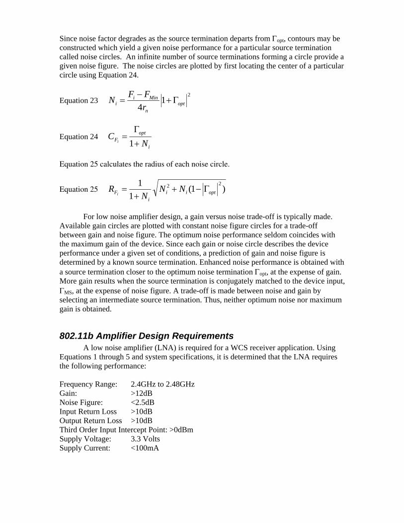
Since noise factor degrades as the source termination departs from Γopt, contours may be constructed which yield a given noise performance for a particular source termination called noise circles. An infinite number of source terminations forming a circle provide a given noise figure. The noise circles are plotted by first locating the center of a particular circle using Equation 24.
Equation 23 2
14 opt
n
Minii r
FFN Γ+−
=
Equation 24 i
optF N
Ci +
Γ=
1
Equation 25 calculates the radius of each noise circle.
Equation 25 )1(1
1 22optii
iF NN
NR
iΓ−+
+=
For low noise amplifier design, a gain versus noise trade-off is typically made.
Available gain circles are plotted with constant noise figure circles for a trade-off between gain and noise figure. The optimum noise performance seldom coincides with the maximum gain of the device. Since each gain or noise circle describes the device performance under a given set of conditions, a prediction of gain and noise figure is determined by a known source termination. Enhanced noise performance is obtained with a source termination closer to the optimum noise termination Γopt, at the expense of gain. More gain results when the source termination is conjugately matched to the device input, ΓMS, at the expense of noise figure. A trade-off is made between noise and gain by selecting an intermediate source termination. Thus, neither optimum noise nor maximum gain is obtained.
802.11b Amplifier Design Requirements A low noise amplifier (LNA) is required for a WCS receiver application. Using
Equations 1 through 5 and system specifications, it is determined that the LNA requires the following performance: Frequency Range: 2.4GHz to 2.48GHz Gain: >12dB Noise Figure: <2.5dB Input Return Loss >10dB Output Return Loss >10dB Third Order Input Intercept Point: >0dBm Supply Voltage: 3.3 Volts Supply Current: <100mA

Several manufacturers produce high performance transistors that are suitable for this particular design. Frequency range, maximum gain, minimum noise figure, and linearity are all considered during the active device selection process. One aspect that is often overlooked during the selection process is whether or not measured s-parameters, noise parameters, and a nonlinear model exist for the chosen transistor. Design cycle times are significantly reduced if nonlinear models and measured s-parameter and noise parameter data is available from the manufacturer. Having the data in electronic form speeds import into the chosen RF/µWave circuit simulator. It is highly recommended that supplied data is verified in a measurement lab if available to ensure its validity before too many design resources are committed to a particular device.
Transistor S-Parameters and Nonlinear Model Several transistors were selected as candidates for the WCS LNA by inspection of corresponding data sheets. Many devices were quickly eliminated since a nonlinear model and measured s-parameters were not available from the particular manufacturer in electronic form. The Avago ATF54143 has measured s-parameter and noise parameter data at various bias conditions and a nonlinear model available in electronic form and specifications that should yield a design with the desired performance. The ATF54143 nonlinear model available from Avago is shown in Figure 3.
Latest ATF-54143curtice ADS MODEL
EqnVar
MSubAdvanced_Curtice2_ModelMESFETM1
AllParams=w Pmax=w Idsmax=w Bvds=w Bvgd=w Bvgs=w Vgfw d=Taumdl=noC=0.1P=0.2R=0.08Fnc=1 MHzN=Eg=
Xti=Imelt=Imax=Ir=Is=Vjr=Vbr=Vbi=0.8R2=R1=Gdrev=Gdfw d=Gsrev=Gsfw d=Crf=0.1 F
Rc=250 OhmCds=0.27 pFLs=Lg=0.18 nHLd=Rs=0.3375 OhmRg=1.0 OhmRd=1.0125 OhmRgd=0.25 OhmFc=0.65Gdcap=2Cgd=0.255 pFCgs=1.73 pFGscap=2Rf=
Rgs=0.25 OhmBetatce=Vtotc=Gamds=1e-4Vgexp=1.91Ucrit=-0.72Idstc=Tnom=16.85Tau=Alpha=13Lambda=82e-3Beta=0.9Vto=0.3PFET=noNFET=yes
Figure 3 – ATF54143model.dsn
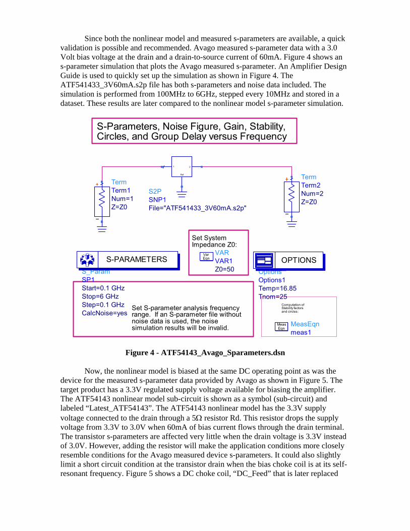
Since both the nonlinear model and measured s-parameters are available, a quick validation is possible and recommended. Avago measured s-parameter data with a 3.0 Volt bias voltage at the drain and a drain-to-source current of 60mA. Figure 4 shows an s-parameter simulation that plots the Avago measured s-parameter. An Amplifier Design Guide is used to quickly set up the simulation as shown in Figure 4. The ATF541433_3V60mA.s2p file has both s-parameters and noise data included. The simulation is performed from 100MHz to 6GHz, stepped every 10MHz and stored in a dataset. These results are later compared to the nonlinear model s-parameter simulation.
S-Parameters, Noise Figure, Gain, Stability,Circles, and Group Delay versus Frequency
Set SystemImpedance Z0:
Set S-parameter analysis frequencyrange. If an S-parameter file without noise data is used, the noisesimulation results will be invalid.
Computation ofStability factorsand circles:
S_ParamSP1
CalcNoise=yesStep=0.1 GHzStop=6 GHzStart=0.1 GHz
S-PARAMETERS
S2PSNP1File="ATF541433_3V60mA.s2p"
21
Ref
VARVAR1Z0=50
EqnVar
TermTerm1
Z=Z0Num=1
TermTerm2
Z=Z0Num=2
OptionsOptions1
Tnom=25Temp=16.85
OPTIONS
MeasEqnmeas1
EqnMeas
Figure 4 - ATF54143_Avago_Sparameters.dsn
Now, the nonlinear model is biased at the same DC operating point as was the
device for the measured s-parameter data provided by Avago as shown in Figure 5. The target product has a 3.3V regulated supply voltage available for biasing the amplifier. The ATF54143 nonlinear model sub-circuit is shown as a symbol (sub-circuit) and labeled “Latest_ATF54143”. The ATF54143 nonlinear model has the 3.3V supply voltage connected to the drain through a 5Ω resistor Rd. This resistor drops the supply voltage from 3.3V to 3.0V when 60mA of bias current flows through the drain terminal. The transistor s-parameters are affected very little when the drain voltage is 3.3V instead of 3.0V. However, adding the resistor will make the application conditions more closely resemble conditions for the Avago measured device s-parameters. It could also slightly limit a short circuit condition at the transistor drain when the bias choke coil is at its self-resonant frequency. Figure 5 shows a DC choke coil, “DC_Feed” that is later replaced

with an inductor in the built-up circuit. Note that the ATF54143 is an enhancement mode FET that requires a positive gate voltage with respect to its source to obtain the desired drain-to-source bias current of 60mA. A voltage divider network is provided by Ra and Rb and is adjusted in the simulator to quickly obtain the required 60mA drain-to-source current. Standard resistor values are used. Ra is arbitrarily set to 33kΩ. Next, Rb is manually adjusted by entering standard resistor values to yield the desired bias current as shown in Figure 5. Note that Rg, the 10kΩ resistor is not necessary for transistor DC bias, but acts as an “all-frequency” choke to effectively isolate the gate from the bias network “RF-wise”. This will be important when the RF aspects of the design are accomplished. Nearly any resistor value is acceptable from a DC bias standpoint since no DC current flows through this resistor. Larger resistor values provide better RF isolation than smaller ones. A smaller resistor can be used in this position if it is determined that the transistor is unstable and requires parallel loading at the input to achieve stability. Adding a bypass capacitor to ground at the Ra, Rb, and Rg junction effectively AC grounds Rg. For now, the 10kΩ resistor is used for the DC simulations and preliminary RF simulations.
RRdR=5 Ohm
DCDC1
DCI_ProbeIdrain
RRgR=10 kOhm
RRbR=6.8 kOhm
RRaR=33 kOhm
DC_FeedDC_Feed1
ATF54143modelX1
Latest_ATF54143
DS1
S2G
V_DCSRC1Vdc=3.3 V
Figure 5 - DCbias.dsn
Figure 6 shows the DC simulation results with Ra set to 33kΩ and Rb set to 6.8kΩ. Note that the drain bias current is nearly 60mA (61.38mA) and the drain voltage is nearly 3 Volt (2.993V). This is close enough to the target bias values.
freq
0.0000 Hz
Idrain.i
61.38 mA
Vd
2.993 V
Figure 6 - DCbias.dds
An s-parameter simulation is now possible on the biased nonlinear model. DC
blocking capacitors and 50Ω terminations are added to the circuit input an output of Figure 5 to obtain the circuit shown in Figure 7. S-parameter simulations are now
Vd

obtained from 100MHz to 6GHz with a frequency step of 10MHz. (The Avago ATF54143 datasheet indicates that device s-parameters were measured on a 20mil thick PCB and recommends connecting two vias in parallel with each other on each source to ground. This was added to the Figure 7 circuit and found to have a minimal effect. The nonlinear model simulated s-parameter data without the ground vias closely matches measured s-parameter data. Thus, the PCB ground vias are not added as indicated in the datasheet.) Figure 8 plots nonlinear model simulated s-parameters and the Avago measured s-parameter data. Note the close similarity between the two s-parameter data sets.
RRdR=5 Ohm
RRgR=10 kOhm
RRbR=6.8 kOhm
RRaR=33 kOhm
S_ParamSP1
Step=10 MHzStop=6.0 GHzStart=100 MHz
S-PARAMETERSDC_FeedDC_Feed1
TermTerm1
Z=50 OhmNum=1
TermTerm2
Z=50 OhmNum=2
DC_BlockDC_Block1
DC_BlockDC_Block2
ATF54143modelX1
Latest_ATF54143
DS1
S2G
V_DCSRC1Vdc=3.3 V
I_ProbeIdrain
Figure 7 – SparametersModel.dsn

freq (100.0MHz to 6.000GHz)
S(1
,1)
SP
ara
me
ters
Mo
de
l..S
(1,1
)
freq (100.0MHz to 6.000GHz)
S(2
,2)
SP
ara
me
ters
Mo
de
l..S
(2,2
)
-30 -20 -10 0 10 20 30-40 40
freq (100.0MHz to 6.000GHz)
S(2
,1)
SP
ara
me
ters
Mo
de
l..S
(2,1
)
-0.10 -0.05 0.00 0.05 0.10-0.15 0.15
freq (100.0MHz to 6.000GHz)
S(1
,2)
SP
ara
me
ters
Mo
de
l..S
(1,2
)
Figure 8 – ATF54143_MeasVsModel_Sparameters.dds

S-Parameter Data Validation It is beneficial to validate data obtained from any vendor if a measurement lab is available. In this case, s-parameter data is measured with an Intercontinental Microwave (ICM) transistor test fixture. The ICM transistor test fixture is used with the appropriate midsection and ICM TOSL-3001 calibration kit. Before calibration is performed, all TOSL-3001 calibration coefficients are loaded into the network analyzer. Each calibration standard has a unique set of coefficients that describe it’s RF response. The ICM calibration coefficients used to describe the TOSL-3001 calibration kit are shown in Tables 1 and 2. The upper frequency limit for the ICM calibration kit is 6GHz. Once the ICM calibration coefficients are loaded into the network analyzer, the TOSL calibration for the transistor test fixture is possible.
Figure 9 shows the measurement setup used to measure ATF54143 s-parameter data. The HP4142B DC Source/Monitor is connected to the E8364B network analyzer bias tees located on the back of that instrument. The HP4142B will supply 3.0 Volts to the Port 2 bias tee and will supply a voltage between 0V and 1V at the Port 1 bias tee. The current sourced from the HP4142B is limited to 100mA to ensure that the 500mA bias tee fuses are not accidentally blown. The HP4142B DC Source/Monitor should be disconnected or turned off during calibration to avoid blowing the port bias fuses in the network analyzer as an added safety precaution. The E8364B network analyzer source power is set to –25dBm to ensure the measured device is not driven into compression during measurement. The network analyzer IF bandwidth is set to 300Hz to limit noise and increase the dynamic range of the measurement system. The TOSL calibration is now performed using the ICM TOSL-3001 calibration kit.
Figure 9 – Transistor S-Parameter Measurement Setup

Table 1
Table 2
Standard Class Assignments Calibration Kit: ICM TOSL-3001
CLASS A B C D E F GStandard
Class LabelS11A 2S11B 1S11C 3S22A 2S22B 1S22C 3Forward Transmission 4Reverse Transmission 4Forward Match 4Reverse Match 4Response 1 2 4Response & Isolation 1 2 4TRL ThruTRL ReflectTRL LineAdapter
TRL OptionCal Z0: _____ System Z0 _____ Line Z0
Set Ref: _____ Thru _____ Reflect
Calibration Kit: ICM TOSL-3001
C0 10-15F
C1 10-27F/Hz
C2 10-36F/Hz2
C3 10-45F/Hz3
# TYPEL0
10-12HL1
10-24H/HzL2
10-33H/Hz2L3
10-42H/Hz3Delay pSec
Z0
ΩLoss GΩ /s MIN MAX
1 SHORT 0 0 0 0 0.49 154.8 0 0 6.1 COAX SHORT
2 OPEN 37.7 4860 -5000 560 0 50 0 0 6.1 COAX OPEN
3 LOAD FIXED 1.485 120.9 0 0 6.1 COAX LOAD
4 THRU 0 50 0 0 6.1 COAX THRU
5
Frequency (GHz)Coax or
WaveguideStandard
Label
STANDARDFixed or Sliding
Terminal Impedance
Ω
Offset

S-Parameters, Noise Figure, Gain, Stability,Circles, and Group Delay versus Frequency
Set SystemImpedance Z0:
Set S-parameter analysis frequencyrange. If an S-parameter file without noise data is used, the noisesimulation results will be invalid.
Computation ofStability factorsand circles:
S2PSNP1File="ATF54143_ICM.s2p"
21
Ref
S_ParamSP1
CalcNoise=yesStep=0.1 GHzStop=6 GHzStart=0.1 GHz
S-PARAMETERSVARVAR1Z0=50
EqnVar
TermTerm1
Z=Z0Num=1
TermTerm2
Z=Z0Num=2
OptionsOptions1
Tnom=25Temp=16.85
OPTIONS
MeasEqnmeas1
EqnMeas
Figure 10 - ATF54143_ICM_Sparameters.dsn
Once calibration is completed and verified, the HP4142B DC Source/Monitor is reconnected or turned back on as shown in Figure 9. Using the HP4142B is a very accurate way of setting/monitoring voltages and currents. First, the 3Volt DC bias is supplied to Port 2 on the network analyzer through the Port 2 bias tee to bias the transistor drain terminal. The HP4142B DC Source/Monitor compliance is set to 100mA so as to limit current into the bias tees. The desired bias current into Port 2 is 60mA, thus the compliance (current limit) is set to 100mA. Essentially, no current is needed to bias the gate of the FET connected to Port 1, so the compliance is set to 10mA. The bias voltage on Port 1, which is connected to the transistor gate through the bias tee, is set to 0.5Volt. Drain current is now measured with the HP4142B DC Source/Monitor and found to be slightly below 60mA. The Port 1 (gate) voltage is slowly increased until 60mA is measured with the HP4142B DC Source/Monitor going into Port 2 – the drain terminal. Once the drain-to-source current is set to 60mA with the drain voltage at 3.0V, the s-parameters are now measured and saved to a Touchstone file. Figure 10 uses an Amplifier Design Guide to plot the lab-measured s-parameters with the simulator.

freq (100.0MHz to 6.000GHz)
S(1
,1)
ICM
_M
ea
sure
d_
S..S
(1,1
)S
Pa
ram
ete
rsM
od
el..
S(1
,1)
freq (100.0MHz to 6.000GHz)
S(2
,2)
ICM
_M
ea
sure
d_
S..S
(2,2
)S
Pa
ram
ete
rsM
od
el..
S(2
,2)
-30 -20 -10 0 10 20 30-40 40
freq (100.0MHz to 6.000GHz)
S(2
,1)
ICM
_M
ea
sure
d_
S..S
(2,1
)S
Pa
ram
ete
rsM
od
el..
S(2
,1)
-0.10 -0.05 0.00 0.05 0.10-0.15 0.15
freq (100.0MHz to 6.000GHz)
S(1
,2)
ICM
_M
ea
sure
d_
S..S
(1,2
)S
Pa
ram
ete
rsM
od
el..
S(1
,2)
Figure 11 - ATF54143_ALL3_Sparameters.dds
A comparison is now made between the Avago measured s-parameters, the nonlinear model generated s-parameters, and the lab measured s-parameters. Figure 11 plots all s-parameter results and shows that all are in close agreement with each other. Since measured data and modeled data are consistent with each other, any of these can be used to proceed with the linear design. Of course, third order intermodulation distortion and gain compression require the nonlinear model for simulation purposes. Noise figure simulation requires linear noise parameters. Noise parameters are included in the s-parameter touchstone file ATF541433_3V60mA.s2p provided by Avago. This s-parameter data file also has data up to 18GHz where as the ICM data is only measured to 6GHz due to the calibration kit frequency limitation. Stability should be considered for all frequencies or at least with data covering as much frequency range as possible. Thus, the Avago measured data is used to simulate stability, available gain, and noise figure.
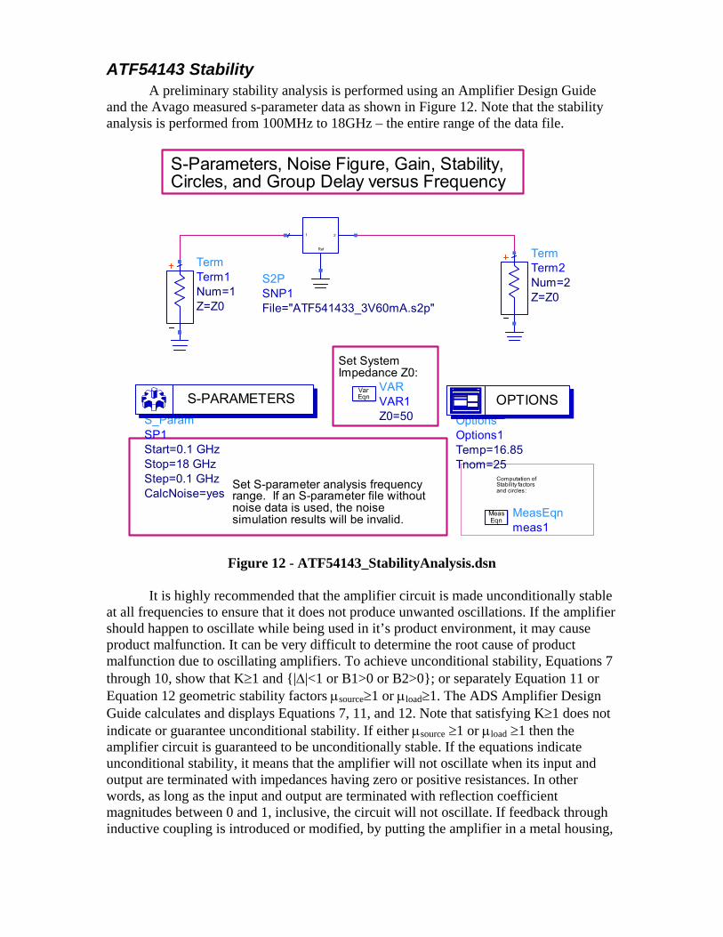
ATF54143 Stability A preliminary stability analysis is performed using an Amplifier Design Guide and the Avago measured s-parameter data as shown in Figure 12. Note that the stability analysis is performed from 100MHz to 18GHz – the entire range of the data file.
S-Parameters, Noise Figure, Gain, Stability,Circles, and Group Delay versus Frequency
Set SystemImpedance Z0:
Set S-parameter analysis frequencyrange. If an S-parameter file without noise data is used, the noisesimulation results will be invalid.
Computation ofStability factorsand circles:
S2PSNP1File="ATF541433_3V60mA.s2p"
21
Ref
S_ParamSP1
CalcNoise=yesStep=0.1 GHzStop=18 GHzStart=0.1 GHz
S-PARAMETERSVARVAR1Z0=50
EqnVar
TermTerm1
Z=Z0Num=1
TermTerm2
Z=Z0Num=2
OptionsOptions1
Tnom=25Temp=16.85
OPTIONS
MeasEqnmeas1
EqnMeas
Figure 12 - ATF54143_StabilityAnalysis.dsn
It is highly recommended that the amplifier circuit is made unconditionally stable
at all frequencies to ensure that it does not produce unwanted oscillations. If the amplifier should happen to oscillate while being used in it’s product environment, it may cause product malfunction. It can be very difficult to determine the root cause of product malfunction due to oscillating amplifiers. To achieve unconditional stability, Equations 7 through 10, show that K≥1 and |∆|<1 or B1>0 or B2>0; or separately Equation 11 or Equation 12 geometric stability factors µsource≥1 or µload≥1. The ADS Amplifier Design Guide calculates and displays Equations 7, 11, and 12. Note that satisfying K≥1 does not indicate or guarantee unconditional stability. If either µsource ≥1 or µload ≥1 then the amplifier circuit is guaranteed to be unconditionally stable. If the equations indicate unconditional stability, it means that the amplifier will not oscillate when its input and output are terminated with impedances having zero or positive resistances. In other words, as long as the input and output are terminated with reflection coefficient magnitudes between 0 and 1, inclusive, the circuit will not oscillate. If feedback through inductive coupling is introduced or modified, by putting the amplifier in a metal housing,

the amplifier may still oscillate. Environmental conditions, such as temperature, can also produce unwanted oscillations. A change in temperature changes the active device s-parameters. To ensure unconditional stability, s-parameters should be taken under all extreme conditions and a stability analysis performed. One other way to ensure stability as far as environmental conditions are concerned is to provide significant margin to the stability conditions. In other words, make K>>1 at all frequencies if possible.
Move marker m1 to select freq point. All listings and impedances on Smith Chartw ill be updated.
f req (100.0MHz to 18.00GHz)
Sop
t
(0.000 to 0.000)
Sop
t_at
_m1
Gam
maS
_at_
freq
_pt
Gam
maL
_at_
freq
_pt
Gam
maL
_wS
opt
indep(Source_stabcir[m1,::]) (0.000 to 51.000)
Sou
rce_
stab
cir[
m1,
::]
indep(Load_stabcir[m1,::]) (0.000 to 51.000)
Load
_sta
bcir[
m1,
::]
Note: if the device (or circuit) is unstable at the freq point, the simultaneous conjugate matching impedances are undefined and GammaL_at_freq_pt and GammaS_at_freq_pt default to 0. Also, MAG is set equal to the maximum stable gain, |S21|/|S12|.
2 4 6 8 10 12 14 160 18
0
10
20
30
-10
40
freq, GHz
Pg
ain
_a
sso
cM
AG
dB
(S2
1)
2 4 6 8 10 12 14 160 18
0.5
1.0
1.5
0.0
2.0
f req, GHz
Km
u_lo
adm
u_so
urce
2.00G
4.00G
6.00G
8.00G
10.0G
12.0G
14.0G
16.0G
0.000
18.0G
m1
RF Frequency Selector
Maximum Available Gain, Associated Pow er Gain (input matched for NFmin, output then conjugately matched), and dB(S21)
2 4 6 8 10 12 14 160 18
2468
101214
0
16
f req, GHz
NF
min
nf(2
)
Stability Factor, K Geometric stability factorsmu_source and mu_load
Minimum Noise Figure, dB,and Noise Figure w ith Z0Ohm terminations
Source and Load Stabil ity Circles; Optimal Source Reflection Coefficients for Mininum NF (Sopt), Simultaneous Conjugate Matching, and Load Reflection Coefficient for Simultaneous Conjugate Matching, and with source matched for NFmin
19.618
MaximumAvailablePow er Gain, dB
0.260 / 145.800
Source ReflectionCoeff icient for Minimum NF
Zopt for NFmin
31.1 + j9.76
Simultaneous Match
Zsource
50.000
Simultaneous Match
Zload
50.000
17.04233.8 + j15.4
Pow er Gain w ith theseSource and Load Reflection Coeff icients
Conjugate Match Load Impedance if Source Reflection Coeff icient is Sopt for Minimum NF
dB(S11)
-4.379
dB(S21)
15.886
dB(S12)
-23.350
dB(S22)
-17.266
Matching For Gain
Matching For Noise Figure
2.400 GHz
RF Frequency
NFmin, dB
0.520
SystemImpedance
50.000
0.886Stability FactorZsource Zload
DUT*
Zopt
Conjugate match Zload if source impedance is Zopt
DUT* *DUT= Dev ice Under Test(simulated circuit or dev ice)
Equations are on the "Equations" page.
If either mu_source or mu_load is >1,the circuit is unconditionally stable.
See also the "Gain, Noise, and Stability Circles" page, and the"S Parameters, Group Delay " page.
Figure 13 - ATF54143_StabilityAnalysis.dss Figure 13 shows the Figure 12 analysis results. This plot was set up using one of
the data display Amplifier Design Guides that correspond to the Stability Analysis Amplifier Design Guide used to set up the simulation. The Amplifier Design Guide plots K, µsource, and µload (Equations 7, 11, and 12) as shown in the red box. Note that the Amplifier Design Guide plots stability factor K, which, on its own, is necessary, but not sufficient to guarantee unconditional stability. Either |∆|, B1, or B2 also have to be plotted to use K as the stability indicator. Satisfying either µsource≥1 or µload≥1 guarantees unconditional stability. Observation of the Stability Factor K, geometric stability factors µsource and µload all indicate potential instability below 4GHz and marginal unconditional stability above 4GHz. (Marginal unconditional stability above 4GHz can only be assessed with µsource and µload since K alone does not indicate unconditional stability.) Above

8GHz, the data looks questionable since the K, µsource, and µload plots have an up-and-down variation associated with them. Since the amplifier is used well below 8GHz, this variation will be ignored to some degree. It is highly recommended that the amplifier is unconditionally stable at all frequencies to ensure that the circuit does not produce unwanted oscillations in or out of the operating frequency band. Thus, it is important to stabilize this device and ensure that unconditional stability exists at all frequencies. At frequencies above 8GHz where variation in K, µsource, and µload are noticed, a stabilizing network that provides significant stability margin is employed so that data inaccuracies can be ignored. Also note, that this is a preliminary stability analysis. If it is not possible to stabilize the ideal circuit without layout and component parasitics and still meet design objectives, it may not be possible to stabilize the device once it is placed in a physical layout. Therefore, an attempt is made to stabilize the device without parasitics. If the device is stabilized and still meets all the performance criteria, then parasitics are added. A new stability analysis is then performed. If the circuit is again unstable, attempts are made to stabilize the device with parasitics. Once the circuit is stable, it is checked to ensure that it still meets its design objectives.
Transistors are stabilized through the use of series and parallel feedback and series and parallel loading at the input and output. A combination of these networks may be necessary to get the desired stability results. Stabilizing network selection and approach depends on the type of device(s) used, the amplifier configuration, and design performance objectives. A common source FET amplifier has a relatively high input reflection coefficient and typically requires input loading to achieve stability. In a low noise amplifier application, however, resistive loss added to the amplifier input degrades noise figure and should be avoided if possible.
An ADS Amplifier Design Guide that stabilizes an unstable circuit is used to stabilize the transistor circuit as shown in Figure 14. The ADS default Amplifier Design Guide has parallel feedback and parallel loading at the input and output. Unconditional stability is desired at all frequencies, thus, the Amplifier Design Guide default stabilizing networks are modified. Series loading (R1) is added at the output, the inductor in the feedback path is removed, and the capacitors CFB and COUT are changed to DC blocking capacitors by setting them to 1uF. Since this amplifier is used in a low noise application, it is desirable to limit loss at the device input, which degrades amplifier noise figure. Thus, capacitor CIN is changed to 0.5pF to limit input loading at the operating frequency since loss added at the input degrades noise figure. The 0.5pF capacitor has a relatively high reactance at 2.5GHz and this reactance decreases with an increase in frequency. This allows input parallel loading at higher frequencies and very little loading at 2.5GHz. This type of loading can be thought of as frequency selective loading. The CIN capacitor is also renamed to C1 such that it is not altered during the optimization process. Input series loading also degrades noise figure. Series loading could be frequency selective as well by putting an inductor in parallel with the load resistor, but inductors typically have higher parasitics than do capacitors, thus input series loading will not be considered in this design. Resistive feedback can also degrade noise figure. In this particular case, the resistive feedback helps stabilize the circuit at low frequencies and has little impact at the operating frequency.
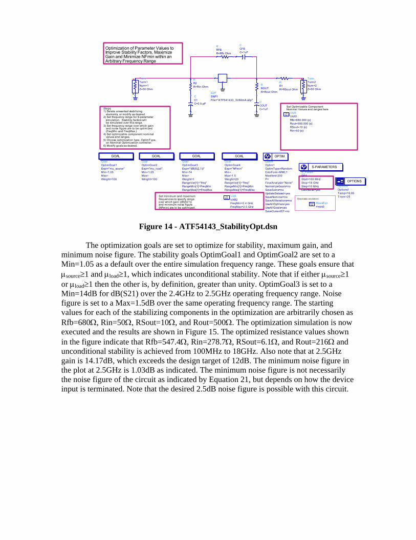
Output data calculations:
Optimization of Parameter Values toImprove Stability Factors, MaximizeGain and Minimize NFmin within anArbitrary Frequency Range
Steps:1) Delete unwanted stabil izing elements, or modify as desired.2) Set frequency range for S-parameter simulation. Stabil ity factors will be simulated over this range.3) Set frequency range over which gain and noise figure are to be optimized (FreqMin and FreqMax.)4) Set optimizable component nominal values and ranges. 5) Choose optimization type, OptimType, on Nominal Optimization controller.6) Modify goals as desired.
Set minimum and maximumfrequencies to specify rangeover which gain (dB(S21))and minimum noise figure(NFmin) are to be optimized.
Set Optimizable Component Nominal Values and ranges here
GoalOptimGoal3
RangeMax[1]=FreqMaxRangeMin[1]=FreqMinRangeVar[1]="freq"Weight=1Max=Min=14Expr="dB(S(2,1))"
GOAL
VARVAR1
Rin=50 oRSout=10 oRout=500.000 oRfb=680.000 o
EqnVar
S_ParamSP1
CalcNoise=yesStep=10 MHzStop=18 GHzStart=100 MHz
S-PARAMETERS
CCOUTC=1uF
CCFBC=1uF
RR2R=Rin Ohm
RR1R=RSout Ohm
GoalOptimGoal1Expr="mu_source"Min=1.05Max=Weight=100
GOAL
GoalOptimGoal2Expr="mu_load"Min=1.05Max=Weight=100
GOAL
GoalOptimGoal4Expr="NFmin"Min=Max=1.5Weight=20RangeVar[1]="freq"RangeMin[1]=FreqMinRangeMax[1]=FreqMax
GOAL
OptimOptim1
SaveCurrentEF=noUseAllGoals=yesUseAllOptVars=yesSaveAllIterations=noSaveNominal=noUpdateDataset=yesSaveSolns=noNormalizeGoals=noFinalAnalysis="None"P=MaxIters=200ErrorForm=MML1OptimType=Random
OPTIM
CC1C=0.5 pF
S2PSNP1File="ATF541433_3V60mA.s2p"
21
Ref
TermTerm1
Z=50 OhmNum=1
TermTerm2
Z=50 OhmNum=2R
ROUTR=Rout Ohm
VARVAR2
FreqMax=2.5 GHzFreqMin=2.4 GHz
EqnVar
MeasEqnmeas3
EqnMeas
OptionsOptions1
Tnom=25Temp=16.85
OPTIONS
RRFBR=Rfb Ohm
Figure 14 - ATF54143_StabilityOpt.dsn
The optimization goals are set to optimize for stability, maximum gain, and
minimum noise figure. The stability goals OptimGoal1 and OptimGoal2 are set to a Min=1.05 as a default over the entire simulation frequency range. These goals ensure that µsource≥1 and µload≥1, which indicates unconditional stability. Note that if either µsource≥1 or µload≥1 then the other is, by definition, greater than unity. OptimGoal3 is set to a Min=14dB for dB(S21) over the 2.4GHz to 2.5GHz operating frequency range. Noise figure is set to a Max=1.5dB over the same operating frequency range. The starting values for each of the stabilizing components in the optimization are arbitrarily chosen as Rfb=680Ω, Rin=50Ω, RSout=10Ω, and Rout=500Ω. The optimization simulation is now executed and the results are shown in Figure 15. The optimized resistance values shown in the figure indicate that Rfb=547.4Ω, Rin=278.7Ω, RSout=6.1Ω, and Rout=216Ω and unconditional stability is achieved from 100MHz to 18GHz. Also note that at 2.5GHz gain is 14.17dB, which exceeds the design target of 12dB. The minimum noise figure in the plot at 2.5GHz is 1.03dB as indicated. The minimum noise figure is not necessarily the noise figure of the circuit as indicated by Equation 21, but depends on how the device input is terminated. Note that the desired 2.5dB noise figure is possible with this circuit.

m3freq=dB(Smatrix(2,1))=14.178optIter=3
2.500GHz
2 4 6 8 10 12 14 160 18
-10
-5
0
5
10
15
-15
20
freq, GHz
dB
m3
Gain, dB(S21)
m3freq=dB(Smatrix(2,1))=14.178optIter=3
2.500GHz
2 4 6 8 10 12 14 160 18
1.5
2.0
2.5
3.0
3.5
4.0
1.0
4.5
freq, GHz
mu_
sour
cem
u_lo
ad
m1freq=NFmin_out=1.027optIter=3
2.500GHz
2 4 6 8 10 12 14 160 18
2
4
6
8
10
12
14
0
16
freq, GHz
dB
m1
Minimum Noise Figure
m1freq=NFmin_out=1.027optIter=3
2.500GHz
Geometrically-Derived Source and Load Stability Factors
If either is >1, the circuit is unconditionally stable.
Cfb <invalid>Rfb
547.4
Lfb <invalid>
Cin <invalid>
Rin
278.7
RSout
6.107
Lout <invalid>
Rout
216.0
Cout <invalid>
Figure 15 - ATF54143_StabilityOpt.dss
Component and layout parasitics are not included in the design as of yet.
Typically, if the preliminary analysis does not meet the design criteria, the final actual circuit with parasitics doesn’t meet the objectives. In other words, parasitics typically degrade RF performance. In this case, the preliminary analysis indicates the transistor and amplifier topology chosen may indeed yield a design that meets all design objectives. Next, some of the component parasitics and preliminary layout parasitics are considered to determine what affects they may have on circuit performance.
Component parasitics include loss and unexpected reactance. Inductors have losses and parasitic capacitance whereas capacitors have loss and parasitic inductance. For this design, an inductor is needed to feed DC bias into the FET drain terminal. Figures 5 and 7 show an ideal DC feed (choke) to inject bias current into the FET drain. A Coilcraft Midi series air-wound inductor replaces the ideal DC feed. The inductor is needed merely to feed DC bias current to the FET drain. Ideally, a very large inductance is needed for the DC feed coil. Inductor parasitic capacitance limits the allowable inductance value due to self-resonance. A 27nH Coil Craft Midi series inductor has a minimum self-resonance frequency of 2.7GHz. This gives the highest possible inductive reactance at the 2.5GHz operating frequency while the inductor self-resonant frequency is still above the amplifier operating frequency.

TLINTL1
F=1198 MHzE=45.12Z=256.5 Ohm
CC1C=.1781 pF
RR2R=.1842 Ohm
RR1R=4.288 Ohm
PortP2Num=2
PortP1Num=1
Figure 16 - CC1812SMS.dsn
Figure 16 shows an equivalent circuit model of the Midi series air-wound inductor
supplied by CoilCraft with part number 1812SMS-27N. Notice the transmission line TL1 in the model. Using a transmission line in this model causes the model to diverge from actual inductor performance at frequencies above self-resonance due to the nature of transmission lines. A subcircuit (CC1812SMS) is now created with the 27nH inductor lumped equivalent circuit for use in the amplifier circuit.
RR1R=240 Ohm
RR4R=620 Ohm
RR2R=220 OhmL
L1
R=L=1.0 pH
S_ParamSP1
Step=10 MHzStop=6.0 GHzStart=10 MHz
S-PARAMETERS
S2PSNP1File="ATF541433_3V60mA.s2p"
21
RefTermTerm1
Z=50 OhmNum=1
TermTerm2
Z=50 OhmNum=2
CC3C=.1 uF
RR3R=10 Ohm
CC1C=0.5 pF
CC2C=.1 uF
RR5R=5 Ohm
CC1812SMSCC27nH
27nH
21
Figure 17 - ATF54143amp1_1pH.dsn
The stabilized circuit is now updated with standard resistor values and the 27nH
bias choke coil subcircuit from Figure 16 as shown in Figure 17. The parallel input load resistor R1 is optimized to 278.7Ω. A 240Ω standard value resistor is used for the parallel input load. The output parallel load resistor R2 optimized to 216Ω. A 220Ω standard value resistor is used for the output parallel load. The series output load R3 optimized to 6.1Ω. A 10Ω standard value resistor is used for the series output load. The feedback resistor R4 optimized to 547.4Ω. A 620Ω standard value resistor is used for the feedback resistor as shown. Figure 5 shows that the 3.3V bias is first fed through a 5Ω resistor R5 before being fed into the choke coil to drop the drain bias from the 3.3V battery voltage

to 3.0V. Note in Figure 17 that the “cold” end of the 27nH inductor is connected in series with this 5Ω resistor. The 3.3V battery is not needed for the s-parameter analysis, but the effects of the bias choke (27nH inductor) is included in the RF simulation. The bias choke and 5Ω resistor series combination is bypassed with the 0.1µF capacitor, C2, as shown in Figure 17. The battery is connected to the 5Ω resistor and 0.1µF capacitor junction in the final circuit. Thus, this node is grounded “RF-wise” due to C2.
Layout parasitics that can wreak havoc on RF circuit performance include ground or lead inductance and parasitic capacitance on the signal path. Minute amounts of ground or lead inductance can cause a calculated unconditionally stable circuit to be unstable. Ground inductance can also cause actual measured circuit gain to be significantly dissimilar to gain predicted with ideal s-parameter simulations. Resistive loading or feedback is used to stabilize a transistor as discussed earlier. Parasitic inductance in the ground or layout traces can effectively isolate such stabilizing circuits from the active device. Parasitic ground inductance in a transistor source or emitter circuit is a form of reactive series feedback that can cause unwanted oscillations. The circuit in Figure 17 includes parasitic ground inductance at the FET source terminal represented by the lumped inductor L1. At this point in the design process, it is helpful to find out how sensitive the circuit may be to this unavoidable parasitic ground inductance. The circuit in Figure 17 has virtually no parasitic ground inductance since the L1 inductance value is set to 1pH, but the inductor is inserted for the analysis. Later, this inductance will be increased to determine what effects it has on final circuit performance. Figure 18 shows an s-parameter plot from the Figure 17 analysis. Both |S11| and |S22| are inside the unit radius Smith chart, which is a necessary, but not sufficient condition for unconditional stability. The dB(S21) plot shows the 50Ω gain of 13.82dB at 2.5GHz which is slightly lower than the 14.17dB of gain predicted by Figures 14 and 15. The lower gain is partly due to the resistor values being changed to standard value resistors and the additional loss added by the 27nH bias tee choke inductor. A stability analysis could be performed on this circuit since the |S11| and |S22| are inside the unit radius Smith chart, but a study of ground inductance effects on circuit performance is now desirable. As mentioned earlier, the lumped inductor L1 in Figure 17 is added to represent parasitic ground inductance. An arbitrary value of 1nH is now used to get an indication on how sensitive the circuit is to parasitic ground inductance. The 1nH inductance value is very small. Higher values of ground inductance are not uncommon in PCB layouts. Figure 19 shows the L1 parasitic ground inductor from Figure 17 is changed to 1nH. Everything else in the circuit remains unchanged. The simulation is now executed from 10MHz to 10GHz.

freq (10.00MHz to 10.00GHz)
S(1
,1)
freq (10.00MHz to 10.00GHz)
S(2
,2)
-8 -6 -4 -2 0 2 4 6 8-10 10
freq (10.00MHz to 10.00GHz)
S(2
,1)
-0.10 -0.05 0.00 0.05 0.10-0.15 0.15
freq (10.00MHz to 10.00GHz)
S(1
,2)
2 4 6 80 10
-10
0
10
-20
20
freq, GHz
dB
(S(2
,1))
m1
m1freq=dB(S(2,1))=13.819
2.500GHz
Figure 18 - ATF54143amp1_1pH.dds

LL1
R=L=1.0 nH
S_ParamSP1
Step=10 MHzStop=10.0 GHzStart=10 MHz
S-PARAMETERS
RR1R=240 Ohm
RR4R=620 Ohm
RR2R=220 Ohm
S2PSNP1File="ATF541433_3V60mA.s2p"
21
RefTermTerm1
Z=50 OhmNum=1
TermTerm2
Z=50 OhmNum=2
CC3C=.1 uF
RR3R=10 Ohm
CC1C=0.5 pF
CC2C=.1 uF
RR5R=5 Ohm
CC1812SMSCC27nH
27nH
21
Figure 19 - ATF54143amp1_1nH.dsn
Figure 20 displays the Figure 19 circuit s-parameters. The |S11| is outside the unit radius Smith chart indicating an input reflection coefficient magnitude greater than unity. This indicates that small amounts of parasitic ground inductance make this circuit potentially unstable at some frequencies. Since the input reflection coefficient magnitude is greater than unity, a stability analysis is not necessary to determine whether or not the amplifier has a propensity to oscillate. Having the output terminated in 50Ω already causes the input reflection coefficient magnitude to become greater than unity, in other words producing negative resistance - a condition needed for oscillation. The dB(S21) plot shows that the 50Ω gain at 2.5GHz is reduced from 13.82dB to 7.48dB. That’s a 6.3dB gain loss from the circuit without parasitic ground inductance. This simple analysis indicates how crucial the layout is with respect to the parasitic ground inductance at the source lead. Every effort is made to minimize layout ground inductance so the amplifier meets the gain requirement and does not oscillate in the application. The analysis also indicates that the stability networks need to load the circuit more out-of-band in case the layout parasitic ground inductance is not low enough. There is no way to totally eliminate the ground inductance, thus, more loading is employed. Since the transistor high input reflection coefficient is causing the problem, loading the output has little affect on stability for this circuit. Currently, the input is loaded with a parallel 240Ω resistor at high frequencies. Loading only occurs at high frequencies because of the 0.5pF capacitor C1. Figure 21 shows the input reflection coefficient plotted on an admittance plane Smith chart. The marker is moved to a location on the trace that has the highest value of negative conductance. Now the reciprocal of the conductance gives the additional parallel load necessary to move the input reflection coefficient magnitude to the edge of the Smith chart. As indicated by the marker, an additional parallel input load of 200Ω is required to move the input reflection coefficient magnitude to unity. The total parallel load is therefore 109Ω. More margin is needed, thus the 240Ω resistor is adjusted to a smaller value and set to 50Ω to stabilize the device input with greater margin. Since the

bypass input loading capacitor is small, the input parallel 50Ω resistor has little contribution to the circuit at 2.5GHz.
freq (10.00MHz to 10.00GHz)
S(1
,1)
freq (10.00MHz to 10.00GHz)
S(2
,2)
-6 -4 -2 0 2 4 6-8 8
freq (10.00MHz to 10.00GHz)
S(2
,1)
-0.4 -0.3 -0.2 -0.1 0.0 0.1 0.2 0.3 0.4-0.5 0.5
freq (10.00MHz to 10.00GHz)
S(1
,2)
2 4 6 80 10
-10
0
10
-20
20
freq, GHz
dB
(S(2
,1))
m1
m1freq=dB(S(2,1))=7.478
2.500GHz
Figure 20 - ATF54143amp1_1nH.dds

freq (10.00MHz to 10.00GHz)
S(1
,1)
m1
m1freq=S(1,1)=1.426 / 67.483admittance = Y0 * (-0.251 - j0.639)
9.340GHz
Figure 21 – ATF54143amp1_1nH_Admittance
RR1R=50 Ohm L
L1
R=L=1.0 nH
S_ParamSP1
Step=10 MHzStop=10.0 GHzStart=10 MHz
S-PARAMETERS
RR4R=620 Ohm
RR2R=220 Ohm
S2PSNP1File="ATF541433_3V60mA.s2p"
21
RefTermTerm1
Z=50 OhmNum=1
TermTerm2
Z=50 OhmNum=2
CC3C=.1 uF
RR3R=10 Ohm
CC1C=0.5 pF
CC2C=.1 uF
RR5R=5 Ohm
CC1812SMSCC27nH
27nH
21
Figure 22 - ATF54143amp1_1nH_Stabilize.dsn
Figure 22 shows the input parallel load resistor set to 50Ω. The parasitic ground inductance is still set to 1nH. Figure 23 shows the analysis results. With the parallel input 50Ω resistor R1, the input reflection coefficient magnitude remains less than unity at all frequencies from 10MHz to 10GHz. The 50Ω gain is 7.47dB which is only 0.01dB less than the case with the 240Ω input parallel resistive load. This shows that the input loading has little affect on the circuit at 2.5GHz due to the 0.5pF capacitor being used as

the bypass, but has a huge affect at higher frequencies. Since both input and output reflection coefficient magnitudes remain less than unity when the circuit input and output is terminated with 50Ω, a stability analysis is now performed. Note that because the input and output reflection coefficient magnitudes are less than unity, doesn’t mean the circuit is unconditionally stable. There may still be source or load terminations other than 50Ω that can cause unwanted oscillations.
freq (10.00MHz to 10.00GHz)
S(1
,1)
freq (10.00MHz to 10.00GHz)S
(2,2
)
-6 -4 -2 0 2 4 6-8 8
freq (10.00MHz to 10.00GHz)
S(2
,1)
-0.4 -0.3 -0.2 -0.1 0.0 0.1 0.2 0.3 0.4-0.5 0.5
freq (10.00MHz to 10.00GHz)
S(1
,2)
2 4 6 80 10
-10
0
10
-20
20
freq, GHz
dB
(S(2
,1))
m1
m1freq=dB(S(2,1))=7.466
2.500GHz
Figure 23 - ATF54143amp1_1nH_Stabilize.dds

S-Parameters, Noise Figure, Gain, Stability,Circles, and Group Delay versus Frequency
Set SystemImpedance Z0:
Set S-parameter analysis frequencyrange. If an S-parameter file without noise data is used, the noisesimulation results will be invalid.
Computation ofStability factorsand circles:
TermTerm1
Z=Z0Num=1
RR1R=50 Ohm L
L1
R=L=1.0 nH
RR4R=620 Ohm
RR2R=220 Ohm
S2PSNP2File="ATF541433_3V60mA.s2p"
21
Ref
CC3C=.1 uF
RR3R=10 Ohm
CC1C=0.5 pF
CC2C=.1 uF
RR5R=5 Ohm
CC1812SMSCC27nH
27nH
21
TermTerm2
Z=Z0Num=2
S_ParamSP1
CalcNoise=yesStep=0.1 GHzStop=18 GHzStart=0.1 GHz
S-PARAMETERSVARVAR1Z0=50
EqnVar
OptionsOptions1
Tnom=25Temp=16.85
OPTIONS
MeasEqnmeas1
EqnMeas
Figure 24 - ATF54143_StabilityAnalysis2.dsn
Figure 24 is a stability analysis from 100MHz to 18GHz with the parasitic ground inductance set to 1nH and the input parallel load resistor set to 50Ω from Figure 22. The 50Ω gain of 7.47dB plotted in Figure 23 is not adequate gain for the 12dB design goal. Stability is checked for the case of 1nH ground inductance before investigating the next case of parasitic ground inductance. Figure 25 is the same ADS Amplifier Design Guide data display from before that plots Equations 7, 11, and 12 – stability factors K, µsource, and µload respectively. The circuit from Figure 24 data indicates potential instability between 6GHz and 9.5GHz as shown in the red box since µsource <1 and µload <1. Before making any further adjustments to stabilizing networks, the parasitic ground inductance L1 is adjusted down to 0.5nH. The 1nH value was arbitrarily chosen to begin with, so it is helpful to see how sensitive the circuit is when the parasitic ground inductance is cut in half. Figure 26 shows the new circuit set up with the 0.5nH parasitic ground inductance L1 for the stability analysis.

Move marker m1 to select freq point. All listings and impedances on Smith Chartw ill be updated.
f req (100.0MHz to 18.00GHz)
Sop
t
(0.000 to 0.000)
Sop
t_at
_m1
Gam
maS
_at_
freq
_pt
Gam
maL
_at_
freq
_pt
Gam
maL
_wS
opt
indep(Source_stabcir[m1,::]) (0.000 to 51.000)
Sou
rce_
stab
cir[
m1,
::]
indep(Load_stabcir[m1,::]) (0.000 to 51.000)
Load
_sta
bcir[
m1,
::]
Note: if the device (or circuit) is unstable at the freq point, the simultaneous conjugate matching impedances are undefined and GammaL_at_freq_pt and GammaS_at_freq_pt default to 0. Also, MAG is set equal to the maximum stable gain, |S21|/|S12|.
2 4 6 8 10 12 14 160 18
-20
-10
0
10
-30
20
freq, GHz
Pg
ain
_a
sso
cM
AG
dB
(S2
1)
2 4 6 8 10 12 14 160 18
0.10.20.30.40.50.60.70.80.9
0.0
1.0
f req, GHz
Km
u_lo
adm
u_so
urce
2.00G
4.00G
6.00G
8.00G
10.0G
12.0G
14.0G
16.0G
0.000
18.0G
m1
RF Frequency Selector
Maximum Available Gain, Associated Pow er Gain (input matched for NFmin, output then conjugately matched), and dB(S21)
2 4 6 8 10 12 14 160 18
5
10
15
20
0
25
f req, GHz
NF
min
nf(2
)
Stability Factor, K Geometric stability factorsmu_source and mu_load
Minimum Noise Figure, dB,and Noise Figure w ith Z0Ohm terminations
Source and Load Stabil ity Circles; Optimal Source Reflection Coefficients for Mininum NF (Sopt), Simultaneous Conjugate Matching, and Load Reflection Coefficient for Simultaneous Conjugate Matching, and with source matched for NFmin
8.362
MaximumAvailablePow er Gain, dB
0.335 / -178.664
Source ReflectionCoeff icient for Minimum NF
Zopt for NFmin
24.9 - j439.m
Simultaneous Match
Zsource
50.968 + j10.295
Simultaneous Match
Zload
88.302 + j21.004
7.80687.8 + j44.4
Pow er Gain w ith theseSource and Load Reflection Coeff icients
Conjugate Match Load Impedance if Source Reflection Coeff icient is Sopt for Minimum NF
dB(S11)
-13.561
dB(S21)
7.775
dB(S12)
-17.870
dB(S22)
-9.268
Matching For Gain
Matching For Noise Figure
2.400 GHz
RF Frequency
NFmin, dB
1.263
SystemImpedance
50.000
1.576Stability FactorZsource Zload
DUT*
Zopt
Conjugate match Zload if source impedance is Zopt
DUT* *DUT= Dev ice Under Test(simulated circuit or dev ice)
Equations are on the "Equations" page.
If either mu_source or mu_load is >1,the circuit is unconditionally stable.
See also the "Gain, Noise, and Stability Circles" page, and the"S Parameters, Group Delay " page.
Figure 25 - ATF54143_StabilityAnalysis2.dds Figure 27 displays the Figure 26 simulation results with ground parasitic inductance set to 0.5nH. K, µsource, and µload are plotted and highlighted in the red box. The plot indicates unconditional stability from 100MHz to 18GHz with more stability margin at higher frequencies as desired. At this stage of the design, it is not yet known how much parasitic ground inductance at the transistor source is contained in the PCB layout because the layout is not yet started. Special attention is given to the layout procedure to ensure that parasitic ground inductance at the transistor source is kept as low as possible. Once the layout is complete, EM simulations give an estimate on the amount of parasitic ground inductance. If estimated parasitic ground inductance is too high on the initial layout, the layout is revised in an attempt to lower the PCB ground inductance parasitic. Once electromagnetic (EM) simulations are performed on grounding and other layout features, a stability and gain analysis with PCB layout parasitics included are performed to ensure the amplifier meets all design objectives.

S-Parameters, Noise Figure, Gain, Stability,Circles, and Group Delay versus Frequency
Set SystemImpedance Z0:
Set S-parameter analysis frequencyrange. If an S-parameter file without noise data is used, the noisesimulation results will be invalid.
Computation ofStability factorsand circles:
LL1
R=L=.5 nH
TermTerm1
Z=Z0Num=1
RR1R=50 Ohm
RR4R=620 Ohm
RR2R=220 Ohm
S2PSNP2File="ATF541433_3V60mA.s2p"
21
Ref
CC3C=.1 uF
RR3R=10 Ohm
CC1C=0.5 pF
CC2C=.1 uF
RR5R=5 Ohm
CC1812SMSCC27nH
27nH
21
TermTerm2
Z=Z0Num=2
S_ParamSP1
CalcNoise=yesStep=0.1 GHzStop=18 GHzStart=0.1 GHz
S-PARAMETERSVARVAR1Z0=50
EqnVar
OptionsOptions1
Tnom=25Temp=16.85
OPTIONS
MeasEqnmeas1
EqnMeas
Figure 26 - ATF54143_StabilityAnalysis3.dsn
The gain, noise figure, and stability plots of Figure 25 show three spikes over the
100MHz to 18GHz frequency range. The transmission line used in the Coilcraft 27nH inductor model causes these spikes in the frequency response plots. The actual Coilcraft inductor does not behave as suggested by the model above its self-resonance frequency. A one-port measurement of the inductor is made using an E8364B network analyzer up to 6GHz and saved to a touchstone file named Lp1812SMS_27NG. This one-port measured data file is now used in the amplifier circuit simulation to more accurately predict the behavior of the amplifier circuit above the self-resonant frequency of the inductor up to 6GHz. It was noticed during the inductor measurement that the results above the self-resonant frequency are sensitive to the position of the inductor in the fixture. These variations cause more variability in the model prediction results above the 2.7GHz inductor self-resonant frequency. In other words, it is more difficult to get the circuit model data to agree with final circuit measured data especially above the inductor self-resonant frequency because of the measurement sensitivity.

Move marker m1 to select freq point. All listings and impedances on Smith Chartw ill be updated.
f req (100.0MHz to 18.00GHz)
Sop
t
(0.000 to 0.000)
Sop
t_at
_m1
Gam
maS
_at_
freq
_pt
Gam
maL
_at_
freq
_pt
Gam
maL
_wS
opt
indep(Source_stabcir[m1,::]) (0.000 to 51.000)
Sou
rce_
stab
cir[
m1,
::]
indep(Load_stabcir[m1,::]) (0.000 to 51.000)
Load
_sta
bcir[
m1,
::]
Note: if the device (or circuit) is unstable at the freq point, the simultaneous conjugate matching impedances are undefined and GammaL_at_freq_pt and GammaS_at_freq_pt default to 0. Also, MAG is set equal to the maximum stable gain, |S21|/|S12|.
2 4 6 8 10 12 14 160 18
-20
-10
0
10
-30
20
freq, GHz
Pg
ain
_a
sso
cM
AG
dB
(S2
1)
2 4 6 8 10 12 14 160 18
1
2
3
4
0
5
f req, GHz
Km
u_lo
adm
u_so
urce
2.00G
4.00G
6.00G
8.00G
10.0G
12.0G
14.0G
16.0G
0.000
18.0G
m1
RF Frequency Selector
Maximum Available Gain, Associated Pow er Gain (input matched for NFmin, output then conjugately matched), and dB(S21)
2 4 6 8 10 12 14 160 18
5
10
15
0
20
f req, GHz
NF
min
nf(2
)
Stability Factor, K Geometric stability factorsmu_source and mu_load
Minimum Noise Figure, dB,and Noise Figure w ith Z0Ohm terminations
Source and Load Stabil ity Circles; Optimal Source Reflection Coefficients for Mininum NF (Sopt), Simultaneous Conjugate Matching, and Load Reflection Coefficient for Simultaneous Conjugate Matching, and with source matched for NFmin
10.779
MaximumAvailablePow er Gain, dB
0.426 / 175.789
Source ReflectionCoeff icient for Minimum NF
Zopt for NFmin
20.2 + j1.54
Simultaneous Match
Zsource
35.202 + j0.588
Simultaneous Match
Zload
79.672 + j21.309
10.49273.9 + j36.3
Pow er Gain w ith theseSource and Load Reflection Coeff icients
Conjugate Match Load Impedance if Source Reflection Coeff icient is Sopt for Minimum NF
dB(S11)
-16.511
dB(S21)
10.381
dB(S12)
-19.541
dB(S22)
-11.984
Matching For Gain
Matching For Noise Figure
2.400 GHz
RF Frequency
NFmin, dB
1.081
SystemImpedance
50.000
1.500Stability FactorZsource Zload
DUT*
Zopt
Conjugate match Zload if source impedance is Zopt
DUT* *DUT= Dev ice Under Test(simulated circuit or dev ice)
Equations are on the "Equations" page.
If either mu_source or mu_load is >1,the circuit is unconditionally stable.
See also the "Gain, Noise, and Stability Circles" page, and the"S Parameters, Group Delay " page.
Figure 27 - ATF54143_StabilityAnalysis3.dds
Figure 28 shows the amplifier circuit with the 27nH inductor one-port s-parameter measurements included in place of the Coilcraft lumped equivalent model. Figure 29 presents the Figure 28 simulation results. The inductor primary self-resonant frequency response is still noticeable in the amplifier frequency response plots as expected, although it is not as pronounced.

S-Parameters, Noise Figure, Gain, Stability,Circles, and Group Delay versus Frequency
Set SystemImpedance Z0:
Set S-parameter analysis frequencyrange. If an S-parameter file without noise data is used, the noisesimulation results will be invalid.
Computation ofStability factorsand circles:
S1PSNP3File="Lp1812SMS_27NG.s1p"
1
RefLL1
R=L=.5 nH
TermTerm1
Z=Z0Num=1
RR1R=50 Ohm
RR4R=620 Ohm
RR2R=220 Ohm
S2PSNP2File="ATF541433_3V60mA.s2p"
21
Ref
CC3C=.1 uF
RR3R=10 Ohm
CC1C=0.5 pF
CC2C=.1 uF
RR5R=5 Ohm
TermTerm2
Z=Z0Num=2
S_ParamSP1
CalcNoise=yesStep=0.1 GHzStop=18 GHzStart=0.1 GHz
S-PARAMETERSVARVAR1Z0=50
EqnVar
OptionsOptions1
Tnom=25Temp=16.85
OPTIONS
MeasEqnmeas1
EqnMeas
Figure 28 - ATF54143_StabilityAnalysis4.dsn
Maximum Available Gain is displayed and highlighted with orange boxes in Figures 27 and 29. The predicted maximum possible gain is around 10.8dB in both figures. This is 1.2dB below the 12dB design goal. Note that this predicted gain value is obtained with an arbitrary estimated amount of transistor source terminal parasitic ground inductance – 0.5nH for Figures 27 and 29. Although the gain is below the target value in these simulations, the gain without parasitic inductance is well above the target value. A matching network is added at the amplifier input. In this case, a parallel inductor followed by a series capacitor is added. These values have not yet been calculated, but a preliminary match analysis indicates that the parallel inductor coming from the 50Ω source followed by a series capacitor going into the transistor input provides a valid matching topology for the amplifier input. The matching design procedure is further explained later for the final input matching analysis. The approximate matching inductor value allows selection from family of inductors that may be used. This allows a layout of the inductor footprint. In this case, a CoilCraft air core inductor from the Mini-Spring family of inductors provides a range of inductors suitable for the input matching network. Next, the amplifier circuit is laid out with special attention to grounding the FET source terminals. Once the layout is completed, an EM simulation predicts parasitic ground inductance at the transistor source terminal. With an estimate of parasitic inductance, new predictions of gain and stability are possible.

Move marker m1 to select freq point. All listings and impedances on Smith Chartw ill be updated.
f req (100.0MHz to 18.00GHz)
Sop
t
(0.000 to 0.000)
Sop
t_at
_m1
Gam
maS
_at_
freq
_pt
Gam
maL
_at_
freq
_pt
Gam
maL
_wS
opt
indep(Source_stabcir[m1,::]) (0.000 to 51.000)
Sou
rce_
stab
cir[
m1,
::]
indep(Load_stabcir[m1,::]) (0.000 to 51.000)
Load
_sta
bcir[
m1,
::]
Note: if the device (or circuit) is unstable at the freq point, the simultaneous conjugate matching impedances are undefined and GammaL_at_freq_pt and GammaS_at_freq_pt default to 0. Also, MAG is set equal to the maximum stable gain, |S21|/|S12|.
2 4 6 8 10 12 14 160 18
-505
101520
-10
25
freq, GHz
Pg
ain
_a
sso
cM
AG
dB
(S2
1)
2 4 6 8 10 12 14 160 18
1
2
3
4
0
5
f req, GHz
Km
u_lo
adm
u_so
urce
2.00G
4.00G
6.00G
8.00G
10.0G
12.0G
14.0G
16.0G
0.000
18.0G
m1
RF Frequency Selector
Maximum Available Gain, Associated Pow er Gain (input matched for NFmin, output then conjugately matched), and dB(S21)
2 4 6 8 10 12 14 160 18
2
4
6
8
10
0
12
f req, GHz
NF
min
nf(2
)
Stability Factor, K Geometric stability factorsmu_source and mu_load
Minimum Noise Figure, dB,and Noise Figure w ith Z0Ohm terminations
Source and Load Stabil ity Circles; Optimal Source Reflection Coefficients for Mininum NF (Sopt), Simultaneous Conjugate Matching, and Load Reflection Coefficient for Simultaneous Conjugate Matching, and with source matched for NFmin
10.799
MaximumAvailablePow er Gain, dB
0.428 / 175.770
Source ReflectionCoeff icient for Minimum NF
Zopt for NFmin
20.1 + j1.55
Simultaneous Match
Zsource
34.445 + j0.709
Simultaneous Match
Zload
82.662 + j16.241
10.53079.3 + j32.4
Pow er Gain w ith theseSource and Load Reflection Coeff icients
Conjugate Match Load Impedance if Source Reflection Coeff icient is Sopt for Minimum NF
dB(S11)
-15.769
dB(S21)
10.394
dB(S12)
-19.528
dB(S22)
-12.099
Matching For Gain
Matching For Noise Figure
2.400 GHz
RF Frequency
NFmin, dB
1.079
SystemImpedance
50.000
1.495Stability FactorZsource Zload
DUT*
Zopt
Conjugate match Zload if source impedance is Zopt
DUT* *DUT= Dev ice Under Test(simulated circuit or dev ice)
Equations are on the "Equations" page.
If either mu_source or mu_load is >1,the circuit is unconditionally stable.
See also the "Gain, Noise, and Stability Circles" page, and the"S Parameters, Group Delay " page.
Figure 29 - ATF54143_StabilityAnalysis4.dds

Amplifier EM/Circuit Co-Simulation and PCB Fabrication The amplifier is built on Arlon 25N, which is available in many standard laminate thicknesses. Arlon 25N has a dielectric constant of 3.38 and a loss tangent of about .0023 at 2.5GHz. Double-sided laminate having 1 once copper on each side, with a 30±3mil thickness is selected for the design. Arlon 25N has a very consistent dielectric constant over frequency and temperature and is easily processed by manufacturers that process standard FR4 PCBs. Since performance specifications are very consistent and repeatable, using the Arlon 25N material greatly enhances the possibility of completing a one-pass design. In other words, the 25N material properties are used in the EM and circuit simulations to get an accurate simulation of PCB and circuit performance before resources are committed to actually building a board. Circuit repeatability from lot-to-lot is also greatly increased due to the repeatability of the Arlon 25N material. Figure 30 shows the amplifier layout top layer and Figure 31 shows the layout bottom layer. All components are located on the top layer as shown by the figures. EM simulations are now performed so that PCB effects can be included in the circuit analysis. Each critical layout node is simulated individually and results combined with a circuit analysis to include PCB effects. The EM/Circuit Co-Simulation feature in ADS is then employed to combine the EM results with the circuit simulation. Linecalc is used to design the input and output 50Ω transmission lines. Each line is 250mil long so that a TRL calibration kit can be used for measurement. Arlon 25N material properties are used in Linecalc to ensure correct line dimensions.
Figure 30 - AvagoEnhGND.dsn – TopMetal
Node 1
Node 2 Node 3
Node 5
Node 4
Node 6

Figure 31 - AvagoEnhGND.dsn – BottomMetal
For the EM analysis, the substrate is first defined using the Arlon 25N material properties and simulated from 10MHz to 10GHz. The “Substrate Layers” are defined as: FreeSpace Boundary: Open Substrate Layer Name: FreeSpace Permittivity: Loss Tangent Real: 1 Loss Tangent: 0 Permeability: Loss Tangent Real: 1 Loss Tangent: 0 Arlon25N Boundary: Interface Substrate Layer Name: Arlon25N Thickness: 30mil Permittivity: Loss Tangent Real: 3.38 Loss Tangent: 0.0023 Permeability: Loss Tangent Real: 1 Loss Tangent: 0 ///GND/// Boundary: Closed Plane: Bulk conductivity in Siemens/meter Conductivity: 5.8E7 The “Metalization Layers” are defined as follows: FreeSpace ----Strip cond Layout Layer: Mapped to TopMetal, Sheet Conductor, Sigma 5.8E7S/m Arlon25N Via Layer: Mapped to Plated Hole ///GND/// Once the substrate is computed, it is used for all PCB parasitic simulations. First, each node is analyzed with the EM simulator to ensure convergence. Once each component
FB
Ground plane removed to limit capacitance.

footprint parasitic is analyzed, a component is created from the Momentum Component menu, which allows the ADS EM/Circuit Co-Simulation capability. Each node is labeled in Figure 30 for reference. Node 1 is labeled in Figure 30 and shown in Figure 32. This node connects the input matching inductor to the amplifier input. The amplifier is first simulated without the input matching network and then with the input matching network. For the first case, the inductor is not connected at the amplifier input. Thus, the inductor footprint pad is connected to the input microstrip line as shown in Figure 30. A “Single” port is used for this EM simulation as shown in Figure 32. The EM simulation creates a one-port s-parameter dataset named AvagoEnhNode1.
Figure 32 - AvagoEnhNode1.dsn
Node 2 is labeled in Figure 30 and shown in Figure 33. This trace connects the input matching capacitor to the transistor gate, the feedback resistor R4 to the transistor gate, and the input parallel load resistor R1 to the transistor gate. Four “Internal” ports are used for the EM simulation setup since each component is soldered to the footprint pad. The ports are connected to each pad center as shown in Figure 33. An EM simulation creates a four-port s-parameter dataset named AvagoEnhNode2 for this PCB trace.
Figure 33 - AvagoEnhNode2.dsn
Node 3 is labeled in Figure 30 and shown in Figure 34. This PCB trace connects the transistor drain to the series and parallel output loads R3 and R2, the transistor drain

to the 27nH bias choke coil, and the transistor drain to a feedback DC blocking capacitor. (The DC feedback blocking capacitor is put in series with feedback resistor R4 to block the DC bias. This DC blocking capacitor was not included in the schematics up to this point.) The footprint pad of the 27nH choke inductor is quite large and would add parasitic capacitance in parallel with the inductor, which in turn, would lower the self-resonant frequency of the bias tee. Figure 34b is the actual trace on the PCB layout. Since there would be a substantial amount of parasitic capacitance on this pad, it was decided that the ground plane would be removed from beneath this pad on the bottom layer (BottomMetal) to limit parasitic capacitance. Figure 31 shows the absence of ground plane under the inductor footprint pad. The EM simulator assumes infinite ground plane in all directions when it is set up in the simple case. Note, that the BottomMetal layer could be defined as a layer in the EM simulator, and then an open boundary layer could be defined below that layer. A ground reference port could be used to reference the BottomMetal layer to ground. This approach would likely be more accurate, but would require much more simulation time. This approach also requires a new substrate definition and simulation for the added layers. Thus, the Arlon25N substrate definition is not usable for the approach where BottomMetal is used as the ground reference. Instead of the more complicated, time consuming approach, the inductor pad was removed and not included on the trace for the EM simulation as shown in Figure 34a. This approach is less accurate, but will simulate much faster and should capture most of the parasitic effects of the trace. When the pad is removed, the fringe capacitance around the edge of that pad would not be included as well as the inductance associated with the pad. Although the pad is not included, an EM simulation should yield a good estimate of the parasitics added by this particular trace. Five “Internal” ports are connected to each pad center with the exception of the inductor pad removed. In this case, an internal port is added to the trace end as shown in Figure 34a. An EM simulation creates a five-port s-parameter dataset named AvagoEnhNode3a for this PCB trace.
Figure 34 - AvagoEnhNode3a.dsn EnhNode3b.dsn
a b

Node 4 is labeled in Figure 30 and shown in Figure 35. This node connects the output parallel load resistor R2 to the parallel load DC blocking capacitor C3. Two “Internal” ports are connected to the pad centers as shown in the figure. An EM simulation of this trace creates a two-port s-parameter dataset called AvagoEnhNode4.
Figure 35 - AvagoEnhNode4.dsn Node 5 is labeled in Figure 30 and is shown in Figure 36. This trace connects the output series load resistor R3 to a series output DC blocking capacitor. The DC blocking capacitor is added to block the DC from the amplifier output. It has not been included in any simulations up to this point. Two “Internal” ports are connected to the pads as shown. An EM simulation of this trace creates a two-port s-parameter dataset called AvagoEnhNode5.
Figure 36 - AvagoEnhNode5.dsn
Node 6 is denoted in Figure 30 and shown in Figure 37. This trace connects the input parallel load resistor R1 to the 0.5pF bypass capacitor C1, and connects gate bias resistors to each other and to the input parallel load resistor R1 and 0.5pF bypass capacitor C1. A four-port s-parameter dataset called AvagoEnhNode6 is created upon execution of an EM simulation of this PCB trace.
Figure 37 - AvagoEnhNode6.dsn
The feedback trace is shown in Figure 31 on the PCB. This trace is on the BottomMetal layer underneath the TopMetal ground plane and connects the feedback

resistor R4 to the feedback capacitor. Thus, for the EM simulation, an assumption is made that the trace is on the top of the PCB so that the existing Arlon25N substrate may be used for the EM simulation. In other words, the BottomMetal layer is mapped to the top of the substrate and the TopMetal layer is mapped to the GND plane. In reality, the runner is actually copied to the TopMetal layer and no mapping of the BottomMetal layer occurs. Thus, the runner in Figure 38 is on the substrate top layer and the bottom layer is a ground plane for the EM simulation. The vias cutting through the PCB on the actual layout are not included in the EM simulation since they would be shorted to ground. The footprint pads for the feedback resistor R4 and feedback DC blocking capacitor are also not included. This is an estimate that includes most of the parasitic effects of the feedback runner. A “Single” port is used on each end of the runner as shown in Figure 38. A two-port s-parameter dataset is created upon completion of the EM simulation.
Figure 38 - AvagoEnhFB.dsn
Finally, an estimate of parasitic ground inductance on the transistor source leads is simulated. The transistor has two source leads that are connected internally to each other. For the source terminal parasitic ground inductance estimate, an EM simulation is performed at the connection point of each transistor source lead on the PCB. Since the transistor s-parameter data uses a two-port representation that has only one ground reference, the inductance value estimates for the two lead connections are combined as parallel inductances to obtain one parasitic ground inductance value for the circuit simulations. According to the Avago 54143 data sheet, the s-parameters are measured in a fixture that has vias tying the source terminals to ground. This adds some uncertainty to the end result of actual amplifier performance versus model performance. An estimate of ground inductance on the PCB layout is accomplished with an EM simulation. The Arlon 25N substrate is set up with an infinite ground plane on the bottom layer. Using this approach is likely to under-estimate the parasitic inductance. An alternate approach changes the bottom layer of the substrate to a strip layer like the top layer and maps the BottomMetal layer to this new bottom strip layer. An open boundary layer is added below the bottom metal layer. A ground reference port is now added to the BottomMetal

layer. Placement of this ground reference port on the BottomMetal layer is problematic. Where is the actual ground reference? No two points on the bottom ground layer are at the exact same RF voltage potential since there is inductance and loss in the ground plane. Thus, placement of the ground reference port will affect analysis results. Parasitic inductance is likely to be higher and more realistic with this approach, but the simulation time is longer. Since an estimate of parasitic ground inductance is the objective, the first method is used for simulation.
Figure 39 shows a portion of the layout where vias connect the top layer metal to the bottom layer metal. An “Internal” port is added to the TopMetal layer where the thin transistor source leg connects to the PCB. The Arlon25N substrate is used for the EM simulation. Edge meshing is not used and the analysis is performed only at 2.5GHz. Upon completion of the EM simulation a one-port s-parameter dataset is created.
Figure 39 - AvagoEnhViasThinLegLessVias.dsn
freq (2.500GHz to 2.500GHz)
m1
S11
m1freq=AvagoEnhViasThinLegLessVias_mom..S(1,1)=1.000 / 175.631impedance = Z0 * (2.278E-4 + j0.038)
2.500GHz
Figure 40 - AvagoEnhViasThinLegLessVias.dds

Figure 40 shows the results of the first parasitic ground inductance simulation. The inductive reactance is j(50×0.038)=j1.9 as shown on the Smith chart marker readout. Solving for the inductance value:
Equation 26 nHf
X L 1214.0)105.2(2
9.12 9 =
×π=
π
Figure 41 - AvagoEnhViasThinLeg.dsn
Figure 41 has 4 additional vias added close to the transistor thin leg in an attempt to lower the parasitic ground inductance. The internal port is in the same location as in Figure 39. The 2.5GHz EM simulation creates a one-port s-parameter dataset. Figure 42 plots the data on a Smith chart as shown. The marker readout yields the inductive reactance j(50×0.017)=j0.85, which is less than half of the parasitic inductive reactance from the first case. Solving for the inductance value:
Equation 27 nHf
X L 0541.0)105.2(2
85.02 9 =
×π=
π
The four extra vias are included in the layout since they lower the parasitic inductance value to less than half.
Figure 43 shows the setup for estimating parasitic ground inductance where the wide transistor source leg connects to the TopMetal layer. The internal port connects where the center of the transistor lead attaches. The EM simulation creates a one-port s-parameter dataset that is plotted in Figure 44. The marker readout lists inductive reactance j(50×0.0505)=j2.526 as shown in the figure. Solving for the inductance value:
Equation 28 nHf
X L 1608.0)105.2(2
526.22 9 =
×π=
π

freq (2.500GHz to 2.500GHz)
m1
S11
m1freq=AvagoEnhViasThinLeg_mom..S(1,1)=1.000 / 178.039impedance = Z0 * (1.504E-4 + j0.017)
2.500GHz
Figure 42 - AvagoEnhViasThinLeg.dds
Figure 43 - AvagoEnhViasWideLeg.dsn

freq (2.500GHz to 2.500GHz)
m1
S11
m1freq=AvagoEnhViasWideLeg_mom..S(1,1)=0.999 / 174.213impedance = Z0 * (3.199E-4 + j0.051)
2.500GHz
Figure 44- AvagoEnhViasWideLeg.dds
The two calculated inductance values of 0.05447nH and 0.1608nH are now put in parallel to obtain an estimate of parasitic inductance. Note that putting the inductance values in parallel with each other is a very crude approach, but will likely give a decent ballpark estimate of parasitic ground inductance. Putting the inductances in parallel yields an estimated parasitic ground inductance of 0.045nH. An alternate approach to putting the inductance values in parallel would be to use the nonlinear model for the simulation since it includes both source leads. Then, the narrow transistor leg calculated parasitic ground inductance is connected to the narrow source leg and the wide leg calculated parasitic ground inductance is connected to the wide source leg and used for simulation. Note also that the Avago measured s-parameter data was measured in a fixture with vias that add parasitic ground inductance. Figure 45 combines the PCB layout node of each PCB layout trace with the circuit component models to EM/Circuit Co-Simulate the entire circuit with layout parasitics. Each PCB trace was first simulated with the EM simulator to produce a multi-port s-parameter dataset.

S1PCC27nHFile="Lp1812SMS_27NG.s1p"1
Ref
S2PDCblk2File="Cs100000pF.s2p"
21
Ref
S1PC2File="Cp100000pF.s1p"
1
Ref
S1PC3File="Cp100000pF.s1p"
1 Ref
RR5R=5 Ohm
RR4R=680 Ohm
RR2R=220 Ohm
RRbR=6.8 kOhm
RRaR=33 kOhm
S_ParamSP1
Step=10 MHzStop=6 GHzStart=1.3 GHz
S-PARAMETERS
RR1R=50 Ohm
AvagoEnhNode3aAvagoEnhNode3a_1ModelType=MW
AvagoEnhNode4AvagoEnhNode4_1ModelType=MW
S2PFBblkFile="Cs100000pF.s2p"
2 1
Ref
RR3R=10 Ohm
AvagoEnhNode5AvagoEnhNode5_1ModelType=MW
TermTerm2
Z=50 OhmNum=2
CC1C=0.5 pF
AvagoEnhNode6AvagoEnhNode6_1ModelType=MW
AvagoEnhFBAvagoEnhFB_1ModelType=MW
AvagoEnhNode1AvagoEnhNode1_1ModelType=MW
AvagoEnhNode2AvagoEnhNode2_1ModelType=MW
S2PDCblk1File="Cs100000pF.s2p"
21
Ref
S2PATF54143File="ATF541433_3V60mA.s2p"
21
Ref
LL1
R=L=.045 nH
TermTerm1
Z=50 OhmNum=1
Figure 45 - ATF54143ampEM.dsn
Figure 45 contains the estimated parasitic ground inductance represented by the L1 inductor. Measured data for the 0.1uF capacitor is included for the DC blocking capacitors and DC bypassing capacitors as well. Figure 46 plots the Figure 45 s-parameter simulation data. Note that the input matching network is not yet included in the Figure 45 schematic. It is useful to analyze amplifier stability results without matching networks since matching networks can decouple the gain block from the measurement system at some frequencies. The 50Ω gain is 14.2dB according to Figure 46. Notice the resonance at 3.3GHz caused by the output choke coil. This resonance is seen in the S11, S22, S21, and S12 plots. The output reflection coefficient is low at low frequencies below the primary resonance. It is therefore, unlikely that the amplifier requires an output matching network. The input reflection coefficient below the primary resonance indicates that a matching network will improve amplifier input return loss. Input matching also impacts amplifier noise figure as indicated by Equation 27.

freq (1.300GHz to 6.000GHz)
S(1
,1)
freq (1.300GHz to 6.000GHz)
S(2
,2)
-6 -4 -2 0 2 4 6-8 8
freq (1.300GHz to 6.000GHz)
S(2
,1)
-0.08 -0.06 -0.04 -0.02 0.00 0.02 0.04 0.06 0.08-0.10 0.10
freq (1.300GHz to 6.000GHz)
S(1
,2)
1.5 2.0 2.5 3.0 3.5 4.0 4.5 5.0 5.51.0 6.0
-5
0
5
10
15
-10
20
freq, GHz
dB(S
(2,1
))
m1
m1freq=dB(S(2,1))=14.210
2.500GHz
Figure 46 - ATF54143ampEM.dds
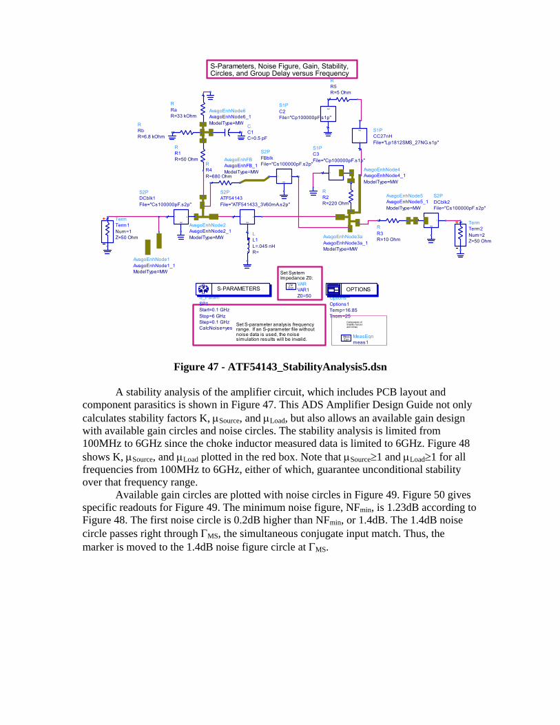
S-Parameters, Noise Figure, Gain, Stability,Circles, and Group Delay versus Frequency
Set SystemImpedance Z0:
Set S-parameter analysis frequencyrange. If an S-parameter file without noise data is used, the noisesimulation results will be invalid.
Computation ofStability factorsand circles:
S1PCC27nHFile="Lp1812SMS_27NG.s1p"1
Ref
S2PDCblk2File="Cs100000pF.s2p"
21
Ref
S1PC2File="Cp100000pF.s1p"
1
Ref
S1PC3File="Cp100000pF.s1p"
1 Ref
RR5R=5 Ohm
RR4R=680 Ohm
RR2R=220 Ohm
RRbR=6.8 kOhm
RRaR=33 kOhm
RR1R=50 Ohm
AvagoEnhNode3aAvagoEnhNode3a_1ModelType=MW
AvagoEnhNode4AvagoEnhNode4_1ModelType=MW
S2PFBblkFile="Cs100000pF.s2p"
2 1
Ref
RR3R=10 Ohm
AvagoEnhNode5AvagoEnhNode5_1ModelType=MW
TermTerm2
Z=50 OhmNum=2
CC1C=0.5 pF
AvagoEnhNode6AvagoEnhNode6_1ModelType=MW
AvagoEnhFBAvagoEnhFB_1ModelType=MW
AvagoEnhNode1AvagoEnhNode1_1ModelType=MW
AvagoEnhNode2AvagoEnhNode2_1ModelType=MW
S2PDCblk1File="Cs100000pF.s2p"
21
Ref
S2PATF54143File="ATF541433_3V60mA.s2p"
21
Ref
LL1
R=L=.045 nH
TermTerm1
Z=50 OhmNum=1
S_ParamSP1
CalcNoise=yesStep=0.1 GHzStop=6 GHzStart=0.1 GHz
S-PARAMETERSVARVAR1Z0=50
EqnVar
OptionsOptions1
Tnom=25Temp=16.85
OPTIONS
MeasEqnmeas1
EqnMeas
Figure 47 - ATF54143_StabilityAnalysis5.dsn
A stability analysis of the amplifier circuit, which includes PCB layout and component parasitics is shown in Figure 47. This ADS Amplifier Design Guide not only calculates stability factors K, µSource, and µLoad, but also allows an available gain design with available gain circles and noise circles. The stability analysis is limited from 100MHz to 6GHz since the choke inductor measured data is limited to 6GHz. Figure 48 shows K, µSource, and µLoad plotted in the red box. Note that µSource≥1 and µLoad≥1 for all frequencies from 100MHz to 6GHz, either of which, guarantee unconditional stability over that frequency range. Available gain circles are plotted with noise circles in Figure 49. Figure 50 gives specific readouts for Figure 49. The minimum noise figure, NFmin, is 1.23dB according to Figure 48. The first noise circle is 0.2dB higher than NFmin, or 1.4dB. The 1.4dB noise circle passes right through ΓMS, the simultaneous conjugate input match. Thus, the marker is moved to the 1.4dB noise figure circle at ΓMS.

Move marker m1 to select freq point. All listings and impedances on Smith Chartw ill be updated.
f req (100.0MHz to 6.000GHz)
Sop
t
(0.000 to 0.000)
Sop
t_at
_m
1G
amm
aS_a
t_fr
eq_
pt
Gam
maL
_at
_fr
eq_
ptG
amm
aL_w
Sop
t
indep(Source_stabcir[m1,::]) (0.000 to 51.000)
So
urce
_sta
bcir[
m1
,::]
indep(Load_stabcir[m1,::]) (0.000 to 51.000)
Load
_st
abci
r[m
1,::
]
Note: if the device (or circuit) is unstable at the freq point, the simultaneous conjugate matching impedances are undefined and GammaL_at_freq_pt and GammaS_at_freq_pt default to 0. Also, MAG is set equal to the maximum stable gain, |S21|/|S12|.
0.5
1.0
1.5
2.0
2.5
3.0
3.5
4.0
4.5
5.0
5.5
0.0
6.0
-50
5101520
-10
25
freq, GHz
Pg
ain
_a
sso
cM
AG
dB
(S2
1)
0.5
1.0
1.5
2.0
2.5
3.0
3.5
4.0
4.5
5.0
5.5
0.0
6.0
1
2
3
4
0
5
f req, GHz
Km
u_lo
ad
mu_
sou
rce
500.M
1.00G
1.50G
2.00G
2.50G
3.00G
3.50G
4.00G
4.50G
5.00G
5.50G
0.000
6.00G
m1
RF Frequency Selector
Maximum Available Gain, Associated Pow er Gain (input matched for NFmin, output then conjugately matched), and dB(S21)
1 2 3 4 50 6
2
4
6
8
0
10
f req, GHz
NF
min
nf(
2)
Stability Factor, K Geometric stability factorsmu_source and mu_load
Minimum Noise Figure, dB,and Noise Figure w ith Z0Ohm terminations
Source and Load Stability Circles; Optimal Source Reflection Coefficients for Mininum NF (Sopt), Simultaneous Conjugate Matching, and Load Reflection Coefficient for Simultaneous Conjugate Matching, and with source matched for NFmin
15.611
MaximumAvailablePow er Gain, dB
0.535 / -169.247
Source ReflectionCoeff icient for Minimum NF
Zopt for NFmin
15.3 - j4.27
Simultaneous Match
Zsource
18.320 - j15.384
Simultaneous Match
Zload
31.439 + j18.314
15.22730.6 + j8.76
Pow er Gain w ith theseSource and Load Reflection Coeff icients
Conjugate Match Load Impedance if Source Reflection Coefficient is Sopt for Minimum NF
dB(S11)
-8.061
dB(S21)
14.521dB(S12)
-23.273
dB(S22)
-17.826
Matching For Gain
Matching For Noise Figure
2.400 GHz
RF Frequency
NFmin, dB
1.231
SystemImpedance
50.000
1.300Stability FactorZsource Zload
DUT*
Zopt
Conjugate match Zload if source impedance is Zopt
DUT* *DUT= Dev ice Under Test(simulated circuit or dev ice)
Equations are on the "Equations" page.
If either mu_source or mu_load is >1,the circuit is unconditionally stable.
See also the "Gain, Noise, and Stability Circles" page, and the"S Parameters, Group Delay " page.
Figure 48 - ATF54143_StabilityAnalysis5 (Page 1)
Eqn num_NFcircles=3
Eqn NFstep_size=.2
Eqn GAstep_size=1Eqn num_GAcircles=3
Set step sizes and number of circles, here.
1.300
Stability Factor, K
Outside
Source Stable Region
Zsource,Source Gamma
Zload,Load Gamma
DUT*
Eqn num_GPcircles=3
Eqn GPstep_size=1
Move marker to desired frequency. Plots willbe updated.
500.M
1.00G
1.50G
2.00G
2.50G
3.00G
3.50G
4.00G
4.50G
5.00G
5.50G
0.000
6.00G
f req, Hz
mRF
RF Frequency Selector
2.400 GHzRF Frequency System Impedance Z0
50.000
indep(rhos) (0.000 to 2000.000)
rho
s
GammaS
indep(Source_stabcir[mRF,::]) (0.000 to 51.000)
So
urc
e_
sta
bc
ir[m
RF
,::]
gain=15.611gain=14.611
gain=13.611gain=12.611
cir_pts (0.000 to 51.000)
GA
cir
cle
s
indep(GammaLopt) (499.000 to 499.000)
Gam
ma
Lo
pt
ns figure=1.431ns figure=1.631ns figure=1.831
Noi
se
_c
irc
les
No
ise
_c
irc
leM
in
Available Gain & Noise Circles,Source Stability CircleSource Gamma.Corresponding Load Gamma, (Black Dot)
indep(rhos) (0.000 to 2000.000)
rho
s GammaL
indep(Load_stabcir[mRF,::]) (0.000 to 51.000)
Lo
ad
_s
tab
cir
[mR
F,:
:] gain=15.611
gain=14.611gain=13.611
gain=12.611
cir_pts (0.000 to 51.000)
GP
cir
cle
s
indep(GammaSopt) (112.000 to 112.000)
Ga
mm
aS
opt
Power Gain Circles,Load Stability CircleLoad Gamma, GammaLCorresponding Source Gamma, (Black Dot)
Move markers GammaS and GammaL to select arbitrary source and load reflection coefficients. The impedances, power gains,and noise figures below will be updated. The transducer power gains are invalid if the markersare moved into the unstable regions (usually inside the stability circles.)
Figure 49 - ATF54143_StabilityAnalysis5 (Page 3)
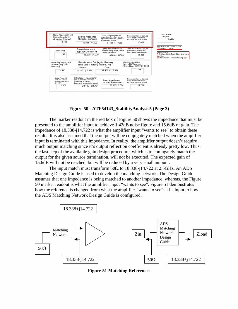
Inside
Load Stable Region
1.231
NFmin,dB
15.278 - j4.270
Source Impedance, Zopt, for Minimum NF
18.338 - j14.722 31.465 + j17.782 15.610
15.227
Source Impedanceat marker GammaS
Optimal load impedance for pow er transfer w hen source impedance is Zopt
Transducer Pow er Gain, dBw hen these source andload impedances are used
30.604 + j8.760
Optimal load impedance for pow er transfer w hen source impedance at marker GammaS is presented to input
Transducer Pow er Gain, dBw hen these source andload impedances are used
1.418
Noise Figure (dB) withSource Impedanceat marker GammaS
15.611
Maximum AvailableGain, dB (MaximumStable Gain, S21/S12) if K<1
Zsource
18.320 - j15.384
Zload
31.439 + j18.314
Simultaneous Conjugate Matching(only valid if stability factor K >1)
1.440
Noise Figure (dB) withZsource (only valid with K>1)
28.182 - j11.774 14.70079.913 - j7.304
Transducer Pow er Gain, dBw hen these source andload impedances are used
Load Impedanceat marker GammaL
Optimal source impedance for pow er transfer w hen load impedance at marker GammaL is presented to output
1.458
Noise Figure (dB) with this optimal source impedance(at right)
Equations are shown on the "Equations2" page.
See also the "NF, Gain, Stab. Fact., Matching" pageand the"S Parameters, Group Delay" page.
Figure 50 - ATF54143_StabilityAnalysis5 (Page 3)
The marker readout in the red box of Figure 50 shows the impedance that must be presented to the amplifier input to achieve 1.42dB noise figure and 15.6dB of gain. The impedance of 18.338-j14.722 is what the amplifier input “wants to see” to obtain these results. It is also assumed that the output will be conjugately matched when the amplifier input is terminated with this impedance. In reality, the amplifier output doesn’t require much output matching since it’s output reflection coefficient is already pretty low. Thus, the last step of the available gain design procedure, which is to conjugately match the output for the given source termination, will not be executed. The expected gain of 15.6dB will not be reached, but will be reduced by a very small amount. The input match must transform 50Ω to 18.338-j14.722 at 2.5GHz. An ADS Matching Design Guide is used to develop the matching network. The Design Guide assumes that one impedance is being matched to another impedance, whereas, the Figure 50 marker readout is what the amplifier input “wants to see”. Figure 51 demonstrates how the reference is changed from what the amplifier “wants to see” at its input to how the ADS Matching Network Design Guide is configured.
Figure 51 Matching References
Matching Network
50Ω
ZloadZin
18.338-j14.722 18.338+j14.72250Ω
ADS Matching Network Design Guide
18.338+j14.722

DA_LEMatch1_untitled1DA_LEMatch1
Zload=18.338+j*14.722 OhmZin=50 OhmF=2.5 GHz
Lumped Element Match Design AssistantNeed Help? Please see the appropriate DesignGuide User Manual
PortP2Num=2
PortP1Num=1
CC1C=1.64 pF
LL1
R=L=2.42 nH
VARVAR1Parameters="#2.5 GHz#50 Ohm#18.338+j*14.722 Ohm#0"
EqnVar
Figure 52 - InMatch_Synthesis.dsn
The input matching network is designed using the ADS Matching Network Design Guide as shown in Figure 52 and demonstrated in Figure 51. An L-match is designed consisting of a parallel 2.42nH inductor next to the 50Ω source and a series 1.64pF capacitor connected to the amplifier input as displayed in Figure 52. Figure 53 adds the ideal input matching network to the Figure 47 amplifier, which contains PCB and lumped component parasitics. Note that the 2.4nH parallel inductor is connected in parallel with the 50Ω source and the 1.6pF series capacitor then connects to the amplifier input. The inductor is not connected to the inductor pad from the Node1 EM simulation since the first Node1 EM simulation is a one-port s-parameter dataset.

S-Parameters, Noise Figure, Gain, Stability,Circles, and Group Delay versus Frequency
Set SystemImpedance Z0:
Set S-parameter analysis frequencyrange. If an S-parameter file without noise data is used, the noisesimulation results will be invalid.
Computation ofStability factorsand circles:
LL3
R=L=2.4 nH
CC5C=1.6 pF
AvagoEnhNode1AvagoEnhNode1_1ModelType=MW
TermTerm1
Z=50 OhmNum=1 L
L1
R=L=.045 nH
S2PATF54143File="ATF541433_3V60mA.s2p"
21
Ref
AvagoEnhNode2AvagoEnhNode2_1ModelType=MW
AvagoEnhFBAvagoEnhFB_1ModelType=MW
AvagoEnhNode6AvagoEnhNode6_1ModelType=MW
CC1C=0.5 pF
TermTerm2
Z=50 OhmNum=2
AvagoEnhNode5AvagoEnhNode5_1ModelType=MW
RR3R=10 Ohm
S2PFBblkFile="Cs100000pF.s2p"
2 1
Ref
AvagoEnhNode4AvagoEnhNode4_1ModelType=MW
AvagoEnhNode3aAvagoEnhNode3a_1ModelType=MW
RR1R=50 Ohm
RRaR=33 kOhm
RRbR=6.8 kOhm
RR2R=220 Ohm
RR4R=680 Ohm
RR5R=5 Ohm
S1PC3File="Cp100000pF.s1p"
1 Ref
S1PC2File="Cp100000pF.s1p"
1
Ref
S2PDCblk2File="Cs100000pF.s2p"
21
Ref
S1PCC27nHFile="Lp1812SMS_27NG.s1p"1
Ref
S_ParamSP1
CalcNoise=yesStep=0.1 GHzStop=6 GHzStart=0.1 GHz
S-PARAMETERSVARVAR1Z0=50
EqnVar
OptionsOptions1
Tnom=25Temp=16.85
OPTIONS
MeasEqnmeas1
EqnMeas
Figure 53 - ATF54143_InMatch.dsn
The Figure 53 s-parameters are plotted in Figure 54. The Smith charts indicate both the input and output are well matched at 2.5GHz. The numeric gain on the S21 polar chart at 2.5GHz is 5.53, which converts to 14.85dB.

m1freq=S(1,1)=0.096 / 9.244impedance = Z0 * (1.208 + j0.038)
2.500GHz
freq (100.0MHz to 6.000GHz)
S(1
,1) m1
m1freq=S(1,1)=0.096 / 9.244impedance = Z0 * (1.208 + j0.038)
2.500GHzm2freq=S(2,2)=0.277 / -121.795impedance = Z0 * (0.674 - j0.344)
2.500GHz
freq (100.0MHz to 6.000GHz)
S(2
,2)
m2
m2freq=S(2,2)=0.277 / -121.795impedance = Z0 * (0.674 - j0.344)
2.500GHz
m3freq=S(2,1)=5.528 / 81.212
2.500GHz
-4 -2 0 2 4-6 6
freq (100.0MHz to 6.000GHz)
S(2
,1)
m3
m3freq=S(2,1)=5.528 / 81.212
2.500GHz
Figure 54 - ATF54143_InMatch.dds
A gain of 15.15dB at 2.4GHz is plotted on the rectangular plot of Figure 55. A 20dB input return loss and 10dB output return loss are also plotted. The predicted noise figure with the input match is 1.56dB at 2.5GHz. A 2.4nH Coilcraft airwound inductor is available for the input matching network. A lumped equivalent model supplied by Coilcraft is shown in Figure 56. The subcircuit model is created for use in the amplifier circuit.

m4freq=dB(S(1,1))=-20.375
2.500GHz
1 2 3 4 50 6
-30
-20
-10
-40
0
freq, GHz
dB
(S(1
,1)) m4
dB
(S(2
,2))
m4freq=dB(S(1,1))=-20.375
2.500GHzm5freq=dB(S(2,1))=15.145
2.400GHz
1 2 3 4 50 6
-30
-20
-10
0
10
-40
20
freq, GHz
dB
(S(2
,1))
m5
m5freq=dB(S(2,1))=15.145
2.400GHz
freq
100.0 MHz200.0 MHz300.0 MHz400.0 MHz500.0 MHz600.0 MHz700.0 MHz800.0 MHz900.0 MHz1.000 GHz1.100 GHz1.200 GHz1.300 GHz1.400 GHz1.500 GHz1.600 GHz1.700 GHz1.800 GHz1.900 GHz2.000 GHz2.100 GHz2.200 GHz2.300 GHz2.400 GHz2.500 GHz2.600 GHz2.700 GHz2.800 GHz2.900 GHz3.000 GHz
nf(2)
46.63334.72527.83723.01719.33816.39613.96811.93110.0028.9257.7096.6555.7394.9444.2573.6693.1692.7522.4102.1511.9371.7761.6661.5991.5621.5621.5931.6501.7301.829
Figure 55 - ATF54143_InMatch.dds
TLINTL1
F=3505 MHzE=33.44Z=94.13 Ohm
RR2R=.015 Ohm
RR1R=11.13 Ohm
CC1C=.0904 pF
PortP2Num=2
PortP1Num=1
Figure 56 - CCA01T.dsn

S-Parameters, Noise Figure, Gain, Stability,Circles, and Group Delay versus Frequency
Set SystemImpedance Z0:
Set S-parameter analysis frequencyrange. If an S-parameter file without noise data is used, the noisesimulation results will be invalid.
Computation ofStability factorsand circles:
CCA01TL3
2.5
nH
21
CC5C=1.6 pF
AvagoEnhNode1AvagoEnhNode1_1ModelType=MW
TermTerm1
Z=50 OhmNum=1
LL1
R=L=.045 nH
S2PATF54143File="ATF541433_3V60mA.s2p"
21
Ref
AvagoEnhNode2AvagoEnhNode2_1ModelType=MW
AvagoEnhFBAvagoEnhFB_1ModelType=MW
AvagoEnhNode6AvagoEnhNode6_1ModelType=MW
CC1C=0.5 pF
TermTerm2
Z=50 OhmNum=2
AvagoEnhNode5AvagoEnhNode5_1ModelType=MW
RR3R=10 Ohm
S2PFBblkFile="Cs100000pF.s2p"
2 1
Ref
AvagoEnhNode4AvagoEnhNode4_1ModelType=MW
AvagoEnhNode3aAvagoEnhNode3a_1ModelType=MW
RR1R=50 Ohm
RRaR=33 kOhm
RRbR=6.8 kOhm
RR2R=220 Ohm
RR4R=680 Ohm
RR5R=5 Ohm
S1PC3File="Cp100000pF.s1p"
1 Ref
S1PC2File="Cp100000pF.s1p"
1
Ref
S2PDCblk2File="Cs100000pF.s2p"
21
Ref
S1PCC27nHFile="Lp1812SMS_27NG.s1p"1
Ref
S_ParamSP1
CalcNoise=yesStep=0.1 GHzStop=6 GHzStart=0.1 GHz
S-PARAMETERSVARVAR1Z0=50
EqnVar
OptionsOptions1
Tnom=25Temp=16.85
OPTIONS
MeasEqnmeas1
EqnMeas
Figure 57 - ATF54143_InMatch2.dsn
The lumped equivalent 2.4nH Coilcraft inductor L3 replaces the ideal inductor in Figure 53 to give the Figure 57 circuit. Figure 58 plots the simulation results of Figure 57. S11 and S22 Smith chart plots indicate that both input and output are very well matched. The input return loss with the inductor model plotted in Figure 59 shows a slight degradation from 20dB to 17.6dB. The 15.14dB gain is unaffected by the slight input loss degradation. The 2.4nH coil loss slightly degrades noise figure to 1.62dB.

m1freq=S(1,1)=0.132 / -50.102impedance = Z0 * (1.158 - j0.238)
2.500GHz
freq (100.0MHz to 6.000GHz)
S(1
,1)
m1
m1freq=S(1,1)=0.132 / -50.102impedance = Z0 * (1.158 - j0.238)
2.500GHzm2freq=S(2,2)=0.241 / -117.312impedance = Z0 * (0.736 - j0.335)
2.500GHz
freq (100.0MHz to 6.000GHz)
S(2
,2)
m2
m2freq=S(2,2)=0.241 / -117.312impedance = Z0 * (0.736 - j0.335)
2.500GHz
Figure 58 - ATF54143_InMatch2.dds
m4freq=dB(S(1,1))=-17.618
2.500GHz
1 2 3 4 50 6
-15
-10
-5
-20
0
freq, GHz
dB(S
(1,1
))
m4
dB(S
(2,2
))
m4freq=dB(S(1,1))=-17.618
2.500GHzm5freq=dB(S(2,1))=15.137
2.400GHz
1 2 3 4 50 6
-20
-10
0
10
-30
20
freq, GHz
dB(S
(2,1
))
m5
m5freq=dB(S(2,1))=15.137
2.400GHz
freq
100.0 MHz200.0 MHz300.0 MHz400.0 MHz500.0 MHz600.0 MHz700.0 MHz800.0 MHz900.0 MHz1.000 GHz1.100 GHz1.200 GHz1.300 GHz1.400 GHz1.500 GHz1.600 GHz1.700 GHz1.800 GHz1.900 GHz2.000 GHz2.100 GHz2.200 GHz2.300 GHz2.400 GHz2.500 GHz2.600 GHz2.700 GHz2.800 GHz2.900 GHz3.000 GHz
nf(2)
46.29734.38527.48822.65618.96416.00713.56511.5139.5748.4837.2616.2065.2964.5143.8483.2882.8252.4512.1571.9501.7881.6811.6221.6051.6161.6581.7261.8161.9242.046
Figure 59 - ATF54143_InMatch2.dds

S_ParamSP1
Step=10 MHzStop=6 GHzStart=1.3 GHz
S-PARAMETERS
S1PLmatchFile="LpA01T.s1p"
1
Ref
AvagoEnhNode1_2AvagoEnhNode1_2_1ModelType=MW
S1PCC27nHFile="Lp1812SMS_27NG.s1p"1
Ref
S2PDCblk2File="Cs100000pF.s2p"
21
Ref
S1PC2File="Cp100000pF.s1p"
1
Ref
S1PC3File="Cp100000pF.s1p"
1 Ref
RR5R=5 Ohm
RR4R=680 Ohm
RR2R=220 Ohm
RRbR=6.8 kOhm
RRaR=33 kOhm
RR1R=50 Ohm
AvagoEnhNode3aAvagoEnhNode3a_1ModelType=MW
AvagoEnhNode4AvagoEnhNode4_1ModelType=MW
S2PFBblkFile="Cs100000pF.s2p"
2 1
Ref
RR3R=10 Ohm
AvagoEnhNode5AvagoEnhNode5_1ModelType=MW
TermTerm2
Z=50 OhmNum=2
CC1C=0.5 pF
AvagoEnhNode6AvagoEnhNode6_1ModelType=MW
AvagoEnhFBAvagoEnhFB_1ModelType=MW
AvagoEnhNode2AvagoEnhNode2_1ModelType=MW
S2PATF54143File="ATF541433_3V60mA.s2p"
21
Ref
LL1
R=L=.045 nH
TermTerm1
Z=50 OhmNum=1
CC5C=1.6 pF
Figure 60 - ATF54143ampEM2.dsn
The Node1 one-port s-parameter EM simulated dataset is replaced by the two-port s-parameter data so that the lumped equivalent circuit model is connected correctly to the PCB trace pad. Previously, the AvagoEnhNode1 was treated as a one-port network and the 2.4nH matching inductor was placed in parallel with that trace representation. Further, and more importantly, the 2.4nH Coil Craft lumped equivalent model is replaced by one-port measured data in Figure 60. The 2.4nH matching inductor attaches to the pad center, thus the updated Node1 trace is used in Figure 60. Figure 61 plots the updated simulation results. The measured data for the 2.4nH input matching inductor indicates that the lumped equivalent model under-estimates loss of the actual inductor. Gain degrades from 15.137dB to 14.65dB and noise figure degrades from 1.6dB to 1.78dB at 2.5GHz as shown by Figures 59 and 61.

freq (1.300GHz to 6.000GHz)
S(1
,1)
m2
m2freq=S(1,1)=0.238 / -70.633impedance = Z0 * (1.050 - j0.500)
2.450GHz
freq (1.300GHz to 6.000GHz)
S(2
,2)
m3
m3freq=S(2,2)=0.214 / -103.262impedance = Z0 * (0.834 - j0.364)
2.450GHz
-6 -4 -2 0 2 4 6-8 8
freq (1.300GHz to 6.000GHz)
S(2
,1)
-0.08 -0.06 -0.04 -0.02 0.00 0.02 0.04 0.06 0.08-0.10 0.10
freq (1.300GHz to 6.000GHz)
S(1
,2)
1.5 2.0 2.5 3.0 3.5 4.0 4.5 5.0 5.51.0 6.0
-5
0
5
10
15
-10
20
freq, GHz
dB
(S(2
,1))
m1
m1freq=dB(S(2,1))=14.646
2.500GHz
freq
2.370 GHz2.380 GHz2.390 GHz2.400 GHz2.410 GHz2.420 GHz2.430 GHz2.440 GHz2.450 GHz2.460 GHz2.470 GHz2.480 GHz2.490 GHz2.500 GHz2.510 GHz2.520 GHz2.530 GHz2.540 GHz2.550 GHz2.560 GHz2.570 GHz2.580 GHz2.590 GHz2.600 GHz2.610 GHz2.620 GHz2.630 GHz
nf(2)
1.7251.7291.7301.7311.7361.7381.7431.7481.7531.7581.7631.7681.7741.7791.7851.7921.7991.8061.8151.8211.8311.8401.8461.8531.8641.8671.875
1.5 2.0 2.5 3.0 3.5 4.0 4.5 5.0 5.51.0 6.0
-15
-10
-5
-20
0
freq, GHz
dB
(S(1
,1))
m4
dB
(S(2
,2))
m5
m4freq=dB(S(1,1))=-12.725
2.500GHzm5freq=dB(S(2,2))=-13.560
2.500GHz
Figure 61 - ATF54143ampEM2.dsn

Amplifier Nonlinear Analysis
FBVload
FB
Two-Tone Harmonic Balance Simulation at one set of input frequencies and powers.
Set Load and Source impedances at baseband,f undamental and harmonic f requencies
Set these v alues:
S1PC3File="Cp100000pF.s1p"
1 Ref
RR2R=220 Ohm
Av agoEnhNode3aAv agoEnhNode3a_1ModelTy pe=MW
Av agoEnhNode4Av agoEnhNode4_1ModelTy pe=MW
RR3R=10 Ohm
Av agoEnhNode5Av agoEnhNode5_1ModelTy pe=MW
S2PDCblk2File="Cs100000pF.s2p"
21
Ref
I_ProbeIload
TermTerm1
Z=Z_loadNum=2
ATF54143modelX1
Latest_ATF54143
DS1
S2G
V_DCSRC1Vdc=3.3 V
RR7R=33 kOhm
RR8R=6.8 kOhm
DC_FeedDC_Feed1
DC_FeedDC_Feed2R
R9R=5 Ohm
V_DCSRC2Vdc=3.3 V
LLs1
R=L=.0545 nH
LLs2
R=L=.161 nH
P_nTonePORT1
P[2]=dbmtow(RFpower-3)P[1]=dbmtow(RFpower-3)Freq[2]=RFf req+f spacing/2Freq[1]=RFf req-f spacing/2Z=Z_sNum=1
S1PLmatchFile="LpA01T.s1p"
1
Ref
Av agoEnhNode1_2Av agoEnhNode1_2_1ModelTy pe=MW
Av agoEnhNode2Av agoEnhNode2_1ModelTy pe=MW
CC5C=1.6 pF
RRbR=6.8 kOhm
RRaR=33 kOhm
RR1R=50 Ohm
CC1C=0.5 pF
Av agoEnhNode6Av agoEnhNode6_1ModelTy pe=MW
RR5R=5 Ohm
S1PC2File="Cp100000pF.s1p"
1
Ref
S1PCC27nHFile="Lp1812SMS_27NG.s1p"1
Ref
Av agoEnhFBAv agoEnhFB_1ModelTy pe=MW
S2PFBblkFile="Cs100000pF.s2p"
2 1
Ref
RR4R=680 Ohm
VARVAR1
Max_IMD_order=7RFpower=-10 _dBmf spacing=5MHzRFf req=2450 MHz
EqnVar
VARglobal VAR6
f _4 = 4.5*RFf reqf _3 = 3.5*RFf reqf _2 = 2.5*RFf reqf _1 = 1.5*RFf reqf _bb=0.5*RFf req
EqnVar
HarmonicBalanceHB1
UseKry lov =y esOrder[2]=7Order[1]=7Freq[2]=RFf req+f spacing/2Freq[1]=RFf req-f spacing/2MaxOrder=Max_IMD_order
HARMONIC BALANCE
VARVAR2Z0=50;Load Impedaneces=Z_l_bb=Z0+j*0Z_l_f und = Z0 + j*0Z_l_2 = Z0 + j*0Z_l_3 = Z0 + j*0Z_l_4 = Z0 + j*0Z_l_5 = Z0 + j*0;Source Impedances=Z_s_bb=Z0+j*0Z_s_f und = Z0 + j*0Z_s_2 = Z0 + j*0Z_s_3 = Z0 + j*0Z_s_4 = Z0 + j*0Z_s_5 = Z0 + j*0
EqnVar
Figure 62 - ATF54143_Amp_HBT2Tone.dsn
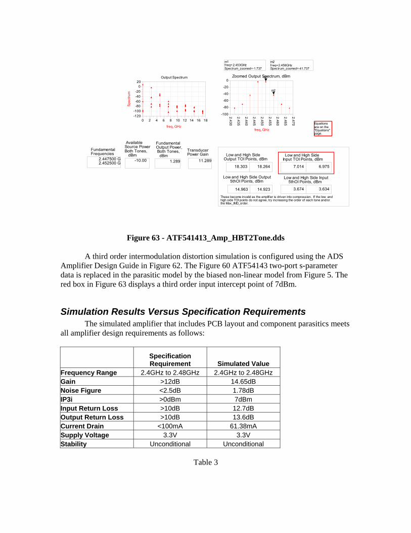
2 4 6 8 10 12 14 160 18
-100
-80-60
-40
-20
0
-120
20
freq, GHzS
pe
ctru
m
Output Spectrum
11.289
Transducer Power Gain
FundamentalFrequencies
1.289
FundamentalOutput Power, Both Tones, dBm
-10.00
Available Source PowerBoth Tones, dBm
18.303 18.264
Low and High Side Output TOI Points, dBm
7.014 6.975
Low and High Side Input TOI Points, dBm
These become invalid as the amplif ier is driven into compression. If the low and high side TOI points do not agree, try increasing the order of each tone and/or the Max_IMD_order.
2.4
35
2.4
40
2.4
45
2.4
50
2.4
55
2.4
60
2.4
65
2.4
30
2.4
70
-80
-60
-40
-20
-100
0
freq, GHz
m1
m2
m1freq=Spectrum_zoomed=-1.737
2.453GHzm2freq=Spectrum_zoomed=-41.737
2.458GHz
2.447500 G2.452500 G
Zoomed Output Spectrum, dBm
14.963 14.923 3.674 3.634
Low and High Side Output 5thOI Points, dBm
Low and High Side Input 5thOI Points, dBm
Equations are on the "Equations" page.
Figure 63 - ATF541413_Amp_HBT2Tone.dds
A third order intermodulation distortion simulation is configured using the ADS Amplifier Design Guide in Figure 62. The Figure 60 ATF54143 two-port s-parameter data is replaced in the parasitic model by the biased non-linear model from Figure 5. The red box in Figure 63 displays a third order input intercept point of 7dBm.
Simulation Results Versus Specification Requirements The simulated amplifier that includes PCB layout and component parasitics meets all amplifier design requirements as follows:
Specification Requirement Simulated Value
Frequency Range 2.4GHz to 2.48GHz 2.4GHz to 2.48GHz Gain >12dB 14.65dB Noise Figure <2.5dB 1.78dB IP3i >0dBm 7dBm Input Return Loss >10dB 12.7dB Output Return Loss >10dB 13.6dB Current Drain <100mA 61.38mA Supply Voltage 3.3V 3.3V Stability Unconditional Unconditional
Table 3

TRL Calibration Kit Since the simulated amplifier with all PCB layout and component parasitics meet
or exceed the specification requirements, the PCB layout of Figures 30 and 31 is fabricated. Additionally, it is convenient to design and construct a TRL calibration kit so that precise measurements are possible without the need of de-embedding procedures. Linecalc is again used to design the TRL calibration standards. Required standards include an Open, Load, Thru, and at least one Line. Since the amplifier input and output 50Ω transmission lines are 250mils long in Figure 30, the Open standard is also 250mils long. The Thru is made twice as long so that a zero length Thru is constructed. Thus, the zero length Thru is 500mils long. The Load standard is used for the isolation calibration and also has a length of 250mils. Next a Line standard is constructed. The Intercontinental Microwave transistor calibration data is valid to 6GHz, thus the TRL calibration Line 1 standard is designed to cover up to 6GHz. The electrical length of the line standard is valid from 30° to 150°. Thus, the Line 1 standard should be no longer electrically than 150° at 6GHz. Using Linecalc, the physical line length is 500mils. Thus, the Line 1 standard is the 500mil electrical length of the zero length Thru standard plus the additional Line 1 length of 500mils, yielding a total Line 1 length of 1000mils. The lowest frequency for the Line 1 standard that yields an electrical length of 30° is just above 1.2GHz, therefore 1.3GHz is used as the Line 1 standard lower frequency limit. Therefore, the Line 1 standard, which is physically 500mils long, covers a frequency range of 1.3GHz to 6GHz. The electrical delay of the Line 1 standard is given by:
Equation 29 pSecmEm
cl r 1.69
sec8997925.266.20127.
==ε
=τ
The TRL zero length Thru standard measures 500mils long and is shown in Figure 64. The TRL Open standard is 250mils long and is shown in Figure 65. The TRL Load standard used for the isolation calibration is 250mils long and shown in Figure 66. The TRL Line 1 standard measures 1000mils long and is shown in Figure 67.

Figure 64 - Thru25N.dsn
Figure 65 - Open25N.dsn

Figure 66 - Load25N.dsn
Figure 67 - Line1_25N.dsn

The Standard Class Assignments for the Arlon 25N TRL calibration kit are shown in Table 4. The Arlon 25N Standard Definitions are shown in Table 5. Other Line standards listed in Tables 4 and 5 are available in the Arlon 25N TRL calibration kit, which are developed in a similar fashion to the Line 1 Calibration Standard.
Table 4
Table 5
Standard Class Assignments Calibration Kit _____Arlon25N
CLASS A B C D E F GStandard
Class LabelS11A 1 OpenS11BS11C 3 LoadS22A 1 OpenS22BS22C 3 LoadForward Transmission 2 ThruReverse Transmission 2 ThruForward Match 2 ThruReverse Match 2 ThruResponseResponse & Isolation 3 Isoln StdTRL Thru 2 ThruTRL Reflect 1 OpenTRL Line 4 5 6 7 8 9 LinesAdapter
TRL OptionCal Z0: _____ System Z0 __X___ Line Z0
Set Ref: ___X__ Thru _____ Reflect
Calibration Kit ___Arlon25N
C0 10-15F
C1 10-27F/Hz
C2 10-36F/Hz2
C3 10-45F/Hz3
# TYPEL0
10-12HL1
10-24H/HzL2
10-33H/Hz2L3
10-42H/Hz3Delay pSec
Z0
ΩLoss GΩ /s MIN MAX
1 Open 0 0 0 0 50 0 50 0.2 20 Open
2 Thru 50 0 50 0.2 20 Thru
3 Load Fixed 50 0 50 0.2 20 Load
4 Line 1 50 69.1 50 1.3 6 1.3-6 Line
5 Line 2 50 207.31 50 0.4 2 0.4-2 Line
6 Line 3 50 19.348 50 4.5 20 4.5-20 Line
7 Line 4 50 20.177 50 4.2 20 4.2-20 Line
8 Line 5 50 96.74 50 0.87 4.3 0.87-4.3 Line
9 Line 6 50 428.42 50 0.2 0.97 0.2-0.97 Line
10
Frequency (GHz)Coax or
WaveguideStandard
Label
STANDARDFixed or Sliding
Terminal Impedance
Ω
Offset
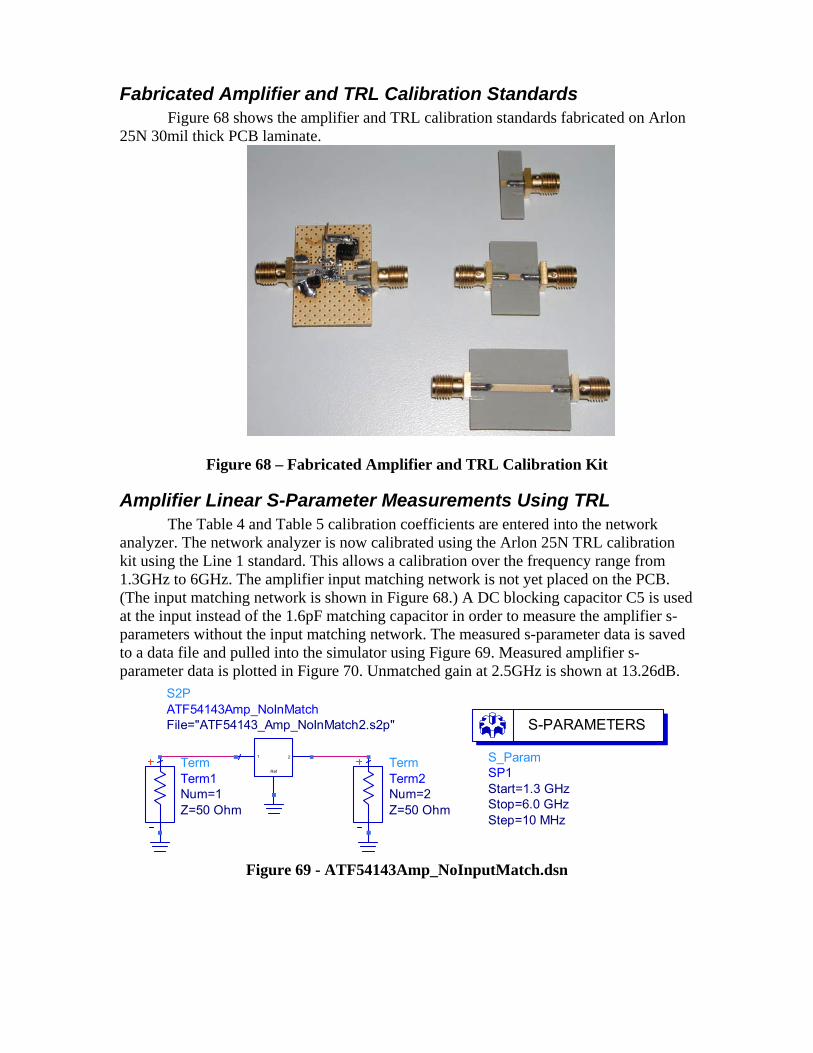
Fabricated Amplifier and TRL Calibration Standards Figure 68 shows the amplifier and TRL calibration standards fabricated on Arlon
25N 30mil thick PCB laminate.
Figure 68 – Fabricated Amplifier and TRL Calibration Kit
Amplifier Linear S-Parameter Measurements Using TRL The Table 4 and Table 5 calibration coefficients are entered into the network analyzer. The network analyzer is now calibrated using the Arlon 25N TRL calibration kit using the Line 1 standard. This allows a calibration over the frequency range from 1.3GHz to 6GHz. The amplifier input matching network is not yet placed on the PCB. (The input matching network is shown in Figure 68.) A DC blocking capacitor C5 is used at the input instead of the 1.6pF matching capacitor in order to measure the amplifier s-parameters without the input matching network. The measured s-parameter data is saved to a data file and pulled into the simulator using Figure 69. Measured amplifier s-parameter data is plotted in Figure 70. Unmatched gain at 2.5GHz is shown at 13.26dB.
S_ParamSP1
Step=10 MHzStop=6.0 GHzStart=1.3 GHz
S-PARAMETERS
S2PATF54143Amp_NoInMatchFile="ATF54143_Amp_NoInMatch2.s2p"
21
Ref
TermTerm2
Z=50 OhmNum=2
TermTerm1
Z=50 OhmNum=1
Figure 69 - ATF54143Amp_NoInputMatch.dsn

freq (1.300GHz to 6.000GHz)
S(1
,1)
freq (1.300GHz to 6.000GHz)
S(2
,2)
-6 -4 -2 0 2 4 6-8 8
freq (1.300GHz to 6.000GHz)
S(2
,1)
-0.06 -0.04 -0.02 0.00 0.02 0.04 0.06-0.08 0.08
freq (1.300GHz to 6.000GHz)
S(1
,2)
1.5 2.0 2.5 3.0 3.5 4.0 4.5 5.0 5.51.0 6.0
-5
0
5
10
15
-10
20
freq, GHz
dB(S
(2,1
))
m1
m1freq=dB(S(2,1))=13.263
2.500GHz
Figure 70 - ATF54143Amp_NoInputMatch.dds

Figure 71 allows a stability analysis on the measured s-parameter data from 1.3GHz to 6GHz. Stability analysis results are plotted in Figure 72. The red box highlights µSource and µLoad plots. Note that µSource≥1 and µLoad≥1 for all frequencies from 1.3GHz to 6GHz, either of which, guarantee unconditional stability over that frequency range. Thus, the measured s-parameters indicate unconditional stability.
S-Parameters, Noise Figure, Gain, Stability,Circles, and Group Delay versus Frequency
Set SystemImpedance Z0:
Set S-parameter analysis frequencyrange. If an S-parameter file without noise data is used, the noisesimulation results will be invalid.
Computation ofStability factorsand circles:
S2PSNP1File="ATF54143_Amp_NoInMatch2.s2p"
21
Ref
S_ParamSP1
CalcNoise=yesStep=0.1 GHzStop=6 GHzStart=1.3 GHz
S-PARAMETERSVARVAR1Z0=50
EqnVar
TermTerm1
Z=Z0Num=1
TermTerm2
Z=Z0Num=2
OptionsOptions1
Tnom=25Temp=16.85
OPTIONS
MeasEqnmeas1
EqnMeas
Figure 71 - ATF54143_StabilityAnalysis6.dsn

Move marker m1 to select freq point. All listings and impedances on Smith Chartw ill be updated.
f req (1.300GHz to 6.000GHz)
Sop
t
(0.000 to 0.000)
Sop
t_at
_m
1G
amm
aS_a
t_fr
eq_
pt
Gam
maL
_at
_fr
eq_
ptG
amm
aL_w
Sop
t
indep(Source_stabcir[m1,::]) (0.000 to 51.000)
So
urce
_sta
bcir[
m1
,::]
indep(Load_stabcir[m1,::]) (0.000 to 51.000)
Load
_st
abci
r[m
1,::
]
Note: if the device (or circuit) is unstable at the freq point, the simultaneous conjugate matching impedances are undefined and GammaL_at_freq_pt and GammaS_at_freq_pt default to 0. Also, MAG is set equal to the maximum stable gain, |S21|/|S12|.
1.5 2.0 2.5 3.0 3.5 4.0 4.5 5.0 5.51.0 6.0
-5
0
5
10
15
-10
20
freq, GHz
Pg
ain
_a
sso
cM
AG
dB
(S2
1)
1.5 2.0 2.5 3.0 3.5 4.0 4.5 5.0 5.51.0 6.0
1
2
3
4
0
5
f req, GHz
Km
u_lo
ad
mu_
sou
rce
1.50G
2.00G
2.50G
3.00G
3.50G
4.00G
4.50G
5.00G
5.50G
1.00G
6.00G
m1
RF Frequency Selector
Maximum Available Gain, Associated Pow er Gain (input matched for NFmin, output then conjugately matched), and dB(S21)
1.5 2.0 2.5 3.0 3.5 4.0 4.5 5.0 5.51.0 6.0
1
2
3
4
0
5
f req, GHz
NF
min
nf(
2)
Stability Factor, K Geometric stability factorsmu_source and mu_load
Minimum Noise Figure, dB,and Noise Figure w ith Z0Ohm terminations
Source and Load Stability Circles; Optimal Source Reflection Coefficients for Mininum NF (Sopt), Simultaneous Conjugate Matching, and Load Reflection Coefficient for Simultaneous Conjugate Matching, and with source matched for NFmin
15.352
MaximumAvailablePow er Gain, dB
0.000 / 0.000
Source ReflectionCoeff icient for Minimum NF
Zopt for NFmin
50.0 + j0.000
Simultaneous Match
Zsource
14.312 - j15.227
Simultaneous Match
Zload
24.279 - j2.481
13.73837.9 - j4.88
Pow er Gain w ith theseSource and Load Reflection Coeff icients
Conjugate Match Load Impedance if Source Reflection Coefficient is Sopt for Minimum NF
dB(S11)
-6.089
dB(S21)
13.642dB(S12)
-25.480
dB(S22)
-16.611
Matching For Gain
Matching For Noise Figure
2.400 GHz
RF Frequency
NFmin, dB
0.000
SystemImpedance
50.000
1.507Stability FactorZsource Zload
DUT*
Zopt
Conjugate match Zload if source impedance is Zopt
DUT* *DUT= Dev ice Under Test(simulated circuit or dev ice)
Equations are on the "Equations" page.
If either mu_source or mu_load is >1,the circuit is unconditionally stable.
See also the "Gain, Noise, and Stability Circles" page, and the"S Parameters, Group Delay " page.
Figure 72 - ATF54143_StabilityAnalysis6.dds
Measured Versus Modeled Figure 73 compares the simulated amplifier using red traces with the measured amplifier using blue traces. Good agreement is shown between the two results. Measured gain at 2.5GHz is 13.26dB whereas the model predicts 14.2dB. Gain is very sensitive to source terminal ground inductance shown by previous analysis. Source terminal inductance is analyzed with EM simulation for both transistor source terminals. Then, these two inductances are combined in parallel to use in the circuit simulation. Some method of combining the two inductances is necessary since an s-parameter linear component in ADS has only one ground reference terminal. The input reflection coefficient at 2.5GHz is slightly higher for the measured amplifier versus the simulated amplifier. This accounts for a portion of the measured amplifier lower gain versus the simulated amplifier in the unmatched case. The method of combining parasitic transistor source terminal inductance and the higher input reflection coefficient of the measured amplifier easily leads to the gain discrepancy between modeled and measured results. Note that the measured amplifier exceeds the 12dB gain requirement.

freq (1.300GHz to 6.000GHz)
S(1
,1)
m2
AT
F5
41
43
am
pE
M..S
(1,1
)
m2freq=S(1,1)=0.496 / 141.271impedance = Z0 * (0.373 + j0.307)
2.400GHz
freq (1.300GHz to 6.000GHz)
S(2
,2)
AT
F5
41
43
am
pE
M..S
(2,2
)
-6 -4 -2 0 2 4 6-8 8
freq (1.300GHz to 6.000GHz)
S(2
,1)
AT
F5
41
43
am
pE
M..S
(2,1
)
-0.08 -0.06 -0.04 -0.02 0.00 0.02 0.04 0.06 0.08-0.10 0.10
freq (1.300GHz to 6.000GHz)
S(1
,2)
AT
F5
41
43
am
pE
M..S
(1,2
)
1.5 2.0 2.5 3.0 3.5 4.0 4.5 5.0 5.51.0 6.0
-5
0
5
10
15
-10
20
freq, GHz
dB
(S(2
,1))
m1
dB
(AT
F5
41
43
am
pE
M..S
(2,1
))
m3
m1freq=dB(S(2,1))=13.263
2.500GHzm3freq=dB(ATF54143ampEM..S(2,1))=14.210
2.500GHz
Figure 73 - ATF54143Amp_NoInMatchCompare.dds
The input matching network is now added by removing the DC blocking capacitor C5 at the amplifier input and replacing it with the 1.6pF matching capacitor and adding the 2.4nH Coil Craft air wound inductor at location L3 (Lmatch). S-parameter

measurements using the TRL calibration procedure are repeated on the amplifier with the matching network in place. Figure 74 brings the measured data into ADS as shown.
S_ParamSP1
Step=10 MHzStop=6 GHzStart=1.3 GHz
S-PARAMETERS
S2PSNP1File="ATF54143_Amp_INMATCH.s2p"
21
RefTermTerm2
Z=50 OhmNum=2
TermTerm1
Z=50 OhmNum=1
Figure 74 - ATF54143_InMatchMeasured.dsn
Figure 75 plots the amplifier measured s-parameter data with the input matching network in place. The measured gain of 13.62dB is shown along with an input return loss of 9.7dB and an output return loss of 13.6dB. The measured gain is slightly below the simulated value (14.2dB) as was the case for the unmatched gain case because of the method used to estimate source ground parasitic inductance. The actual gain exceeds the 12dB specification requirement with margin, and is therefore acceptable. Note that the input return loss of 9.7dB marginally fails to the 10dB specification requirement, but will also be accepted in this particular design since the input return loss is considered to be a “soft” or negotiable specification. The output return loss of 13.64dB exceeds the 10dB goal with some margin. Figure 76 plots the simulated amplifier on the same graphs as the measured amplifier for an easier comparison. Note that the plots show a close agreement between simulated and measured data. The noise figure and third order intercept point are now measured on the amplifier and compared to the simulated values. Noise figure is measured at 1.91dB and input third order intercept point at 2.45GHz is 13.6dBm. The simulated noise figure of 1.78dB closely predicts the measured value. The measured third order input intercept point of 13.7dBm is substantially better than the 7dBm simulated value. An Avago representative confirms that nonlinear performance of the actual device is somewhat better than modeled performance. Note that the measured nonlinear performance is significantly better than the 0dBm specification requirement.

freq (1.300GHz to 6.000GHz)
S(1
,1)
m1
m1freq=S(1,1)=0.327 / -102.412impedance = Z0 * (0.716 - j0.512)
2.500GHz
freq (1.300GHz to 6.000GHz)
S(2
,2)
m2
m2freq=S(2,2)=0.208 / 160.653impedance = Z0 * (0.666 + j0.096)
2.500GHz
-4 -2 0 2 4-6 6
freq (1.300GHz to 6.000GHz)
S(2
,1)
m3
m3freq=S(2,1)=4.795 / 58.923
2.500GHz
1.5 2.0 2.5 3.0 3.5 4.0 4.5 5.0 5.51.0 6.0
-20
-15
-10
-5
-25
0
freq, GHz
dB(S
(1,1
))
m4
dB(S
(2,2
))
m6
m4freq=dB(S(1,1))=-9.711
2.500GHzm6freq=dB(S(2,2))=-13.641
2.500GHz
1.5 2.0 2.5 3.0 3.5 4.0 4.5 5.0 5.51.0 6.0
-5
0
5
10
15
-10
20
freq, GHz
dB(S
(2,1
))
m5
m5freq=dB(S(2,1))=13.616
2.500GHz
Figure 75 - ATF54143_InMatchMeasured.dds

freq (1.300GHz to 6.000GHz)
S(1
,1)
m2
AT
F54
143_
InM
atch
Mea
sure
d..S
(1,1
)
m5
m2freq=S(1,1)=0.238 / -70.633impedance = Z0 * (1.050 - j0.500)
2.450GHz
m5freq=ATF54143_InMatchMeasured..S(1,1)=0.330 / -96.032impedance = Z0 * (0.756 - j0.558)
2.450GHz
freq (1.300GHz to 6.000GHz)S
(2,2
)
m3
AT
F54
143_
InM
atch
Mea
sure
d..S
(2,2
)
m6
m3freq=S(2,2)=0.214 / -103.262impedance = Z0 * (0.834 - j0.364)
2.450GHz
m6freq=ATF54143_InMatchMeasured..S(2,2)=0.197 / 163.539impedance = Z0 * (0.679 + j0.079)
2.450GHz
-6 -4 -2 0 2 4 6-8 8
freq (1.300GHz to 6.000GHz)
S(2
,1)
m7
AT
F54
143_
InM
atch
Mea
sure
d..S
(2,1
) m8
m7freq=S(2,1)=5.513 / 72.982
2.450GHz
m8freq=ATF54143_InMatchMeasured..S(2,1)=4.921 / 64.364
2.450GHz
-0.08 -0.06 -0.04 -0.02 0.00 0.02 0.04 0.06 0.08-0.10 0.10
freq (1.300GHz to 6.000GHz)
S(1
,2)
AT
F54
143_
InM
atch
Mea
sure
d..S
(1,2
)
1.5 2.0 2.5 3.0 3.5 4.0 4.5 5.0 5.51.0 6.0
-5
0
5
10
15
-10
20
freq, GHz
dB(S
(2,1
))
m1
dB(A
TF
5414
3_In
Mat
chM
easu
red.
.S(2
,1))
m4
m1freq=dB(S(2,1))=14.646
2.500GHzm4freq=dB(ATF54143_InMatchMeasured..S(2,1))=13.616
2.500GHz
Figure 76 - ATF54143_AmpCompare.dds

Conclusion The simulated and measured amplifier that includes PCB layout and component
parasitics meets all amplifier design requirements as illustrated in Table 6:
Specification Requirement Simulated Value Measured Value
Frequency Range 2.4GHz to 2.48GHz 2.4GHz to 2.48GHz 2.4GHz to 2.48GHz Gain >12dB 14.65dB 13.62dB Noise Figure <2.5dB 1.78dB 1.91dB IP3i >0dBm 6.9dBm 13.7dBm Input Return Loss >10dB 12.7dB 9.7dB Output Return Loss >10dB 13.6dB 13.6dB Current Drain <100mA 61.38mA 63mA Supply Voltage 3.3V 3.3V 3.3V Stability Unconditional Unconditional Unconditional
Table 6
Table 6 indicates that the first-pass amplifier exceeds most of the requirements. The input return loss is marginal but acceptable. The input match could be adjusted slightly to improve input return loss at the possible expense of noise figure. One of the main objectives was to obtain a working design with the first pass layout. The procedure is considered successful as long as the layout does not have to be altered to obtain a working circuit. The procedure is also considered a success if the components had to be slightly adjusted to achieve performance without a layout modification. In this case, the circuit components did not require adjustment to meet the objectives.
Using the EM/Circuit Co-Simulation capability in ADS allows a first-pass design. Careful attention to layout and simulation results speeds the design process and provides a design cost savings by avoiding multiple pass PCB designs. Note also that the entire PCB does not have to be simulated with the EM simulator to obtain good results. Putting the entire PCB in the simulator may improve the results at the expense of significantly longer simulation time.

References Agilent Technologies, Product Note 8510-8A, Agilent Network Analysis Applying the 8510 TRL Calibration for Non-Coaxial Measurements, Agilent Technologies, 2000. Les Besser, Applied RF Techniques I, Besser Associates, Los Altos, CA, 1995. Guillermo Gonzalez, Microwave Transistor Amplifiers Analysis and Design, Prentice-Hall, Inc., Englewood Cliffs, NJ, 1984. H. L. Krauss, W. Bostian, and F. H. Raab, Solid State Radio Engineering, John Wiley & Sons, NY, 1980. Mario A. Maury, Jr., Steven L. March, Gary R. Simpson, Application Note 5A-017 LRL Calibration of Vector Network Analyzers, Maury Microwave Corporation, 1999. Ken Payne, Wireless Measurements, Theory and Practice, Besser Associates, Los Altos, CA, 1998. KEN PAYNE began his engineering career at RCA, developing circularly polarized TV and FM broadcast antennas and feed systems. He was also involved with wide bandwidth receivers and transmitters, covering from DC to 1GHz, for fiber-optic test equipment. Later, at Motorola's Communications Division, he designed RF amplifiers, mixers, filters, oscillators, antennas and other transceiver circuits and systems for two-way portable and paging products. He developed and directed circuit and system design projects and created a wide range of active and passive RF device models for the HP-EEsof Microwave Design System (MDS) and Advanced Design System (ADS). In addition, Ken also developed RF and microwave design automation, measurement techniques, and interfaces between design workstations and test equipment. As a sideline, he conducted seminars and wrote articles on design methodologies for high performance, low-cost, and high-yield wireless communication circuits and systems. Ken was an instructor for Besser Associates and CEI of Europe for many years where he gave training seminars on RF design and measurement methodologies. Ken was one of the authors of the Oscillator Design Guide available in ADS. Ken now provides consulting services in RF/microwave design.

专注于微波、射频、天线设计人才的培养 易迪拓培训 网址:http://www.edatop.com
射 频 和 天 线 设 计 培 训 课 程 推 荐
易迪拓培训(www.edatop.com)由数名来自于研发第一线的资深工程师发起成立,致力并专注于微
波、射频、天线设计研发人才的培养;我们于 2006 年整合合并微波 EDA 网(www.mweda.com),现
已发展成为国内最大的微波射频和天线设计人才培养基地,成功推出多套微波射频以及天线设计经典
培训课程和 ADS、HFSS 等专业软件使用培训课程,广受客户好评;并先后与人民邮电出版社、电子
工业出版社合作出版了多本专业图书,帮助数万名工程师提升了专业技术能力。客户遍布中兴通讯、
研通高频、埃威航电、国人通信等多家国内知名公司,以及台湾工业技术研究院、永业科技、全一电
子等多家台湾地区企业。
易迪拓培训课程列表:http://www.edatop.com/peixun/rfe/129.html
射频工程师养成培训课程套装
该套装精选了射频专业基础培训课程、射频仿真设计培训课程和射频电
路测量培训课程三个类别共 30 门视频培训课程和 3 本图书教材;旨在
引领学员全面学习一个射频工程师需要熟悉、理解和掌握的专业知识和
研发设计能力。通过套装的学习,能够让学员完全达到和胜任一个合格
的射频工程师的要求…
课程网址:http://www.edatop.com/peixun/rfe/110.html
ADS 学习培训课程套装
该套装是迄今国内最全面、最权威的 ADS 培训教程,共包含 10 门 ADS
学习培训课程。课程是由具有多年 ADS 使用经验的微波射频与通信系
统设计领域资深专家讲解,并多结合设计实例,由浅入深、详细而又
全面地讲解了 ADS 在微波射频电路设计、通信系统设计和电磁仿真设
计方面的内容。能让您在最短的时间内学会使用 ADS,迅速提升个人技
术能力,把 ADS 真正应用到实际研发工作中去,成为 ADS 设计专家...
课程网址: http://www.edatop.com/peixun/ads/13.html
HFSS 学习培训课程套装
该套课程套装包含了本站全部 HFSS 培训课程,是迄今国内最全面、最
专业的HFSS培训教程套装,可以帮助您从零开始,全面深入学习HFSS
的各项功能和在多个方面的工程应用。购买套装,更可超值赠送 3 个月
免费学习答疑,随时解答您学习过程中遇到的棘手问题,让您的 HFSS
学习更加轻松顺畅…
课程网址:http://www.edatop.com/peixun/hfss/11.html
`

专注于微波、射频、天线设计人才的培养 易迪拓培训 网址:http://www.edatop.com
CST 学习培训课程套装
该培训套装由易迪拓培训联合微波 EDA 网共同推出,是最全面、系统、
专业的 CST 微波工作室培训课程套装,所有课程都由经验丰富的专家授
课,视频教学,可以帮助您从零开始,全面系统地学习 CST 微波工作的
各项功能及其在微波射频、天线设计等领域的设计应用。且购买该套装,
还可超值赠送 3 个月免费学习答疑…
课程网址:http://www.edatop.com/peixun/cst/24.html
HFSS 天线设计培训课程套装
套装包含 6 门视频课程和 1 本图书,课程从基础讲起,内容由浅入深,
理论介绍和实际操作讲解相结合,全面系统的讲解了 HFSS 天线设计的
全过程。是国内最全面、最专业的 HFSS 天线设计课程,可以帮助您快
速学习掌握如何使用 HFSS 设计天线,让天线设计不再难…
课程网址:http://www.edatop.com/peixun/hfss/122.html
13.56MHz NFC/RFID 线圈天线设计培训课程套装
套装包含 4 门视频培训课程,培训将 13.56MHz 线圈天线设计原理和仿
真设计实践相结合,全面系统地讲解了 13.56MHz线圈天线的工作原理、
设计方法、设计考量以及使用 HFSS 和 CST 仿真分析线圈天线的具体
操作,同时还介绍了 13.56MHz 线圈天线匹配电路的设计和调试。通过
该套课程的学习,可以帮助您快速学习掌握 13.56MHz 线圈天线及其匹
配电路的原理、设计和调试…
详情浏览:http://www.edatop.com/peixun/antenna/116.html
我们的课程优势:
※ 成立于 2004 年,10 多年丰富的行业经验,
※ 一直致力并专注于微波射频和天线设计工程师的培养,更了解该行业对人才的要求
※ 经验丰富的一线资深工程师讲授,结合实际工程案例,直观、实用、易学
联系我们:
※ 易迪拓培训官网:http://www.edatop.com
※ 微波 EDA 网:http://www.mweda.com
※ 官方淘宝店:http://shop36920890.taobao.com
专注于微波、射频、天线设计人才的培养
官方网址:http://www.edatop.com 易迪拓培训 淘宝网店:http://shop36920890.taobao.com