tutorial ads 1 -...
TRANSCRIPT

Simulation of a 2.4 GHz Patch Antenna using ADS Momentum
a Tutorial by
Nader Behdad
EEL 6463, Spring 2007

ADS Momentum Tutorial No. 1, Rev. 1, by Nader Behdad ([email protected])
EEL 6463: Antennas II Spring 2007, University of Central Florida
2
1. Start ADS and create a new project by selecting “File New Project” item. You can call this project Tutorial. Start a new layout by clicking on the “New Layout
Window” button ( ). A new layout drawing window appear. This is shown in Figure 1.
Figure 1. Momentum layout window.
2. Select “Momentum Substrate Create/Modify” item. The “Create/Modify
Substrate” window pops up. This window is shown in Figure 2. In this window, you can define the substrate parameters and metal layers and properties all in one place. Under the “Substrate Layers” tab, you can define the layers of dielectric. In this case, we have a microstrip fed patch antenna that is fabricated on a 60 mil thick RO4003 substrate. Therefore, we have only one dielectric layer that has an infinitely large ground plane on one side and free space on the other side; the default dielectric layer is Alumina. You can change the name to RO4003C and change the thickness to 60 mils. Momentum allows for entering the dielectric parameters in three different formats. You can use the Real and Imaginary parts of the dielectric constant ( εεε ′′−′= jr ), the real part of the dielectric constant in conjunction with its loss tangent ( εεδ ′′′= /)tan( , or the real part of the dielectric constant in conjunction with the conductivity of the material. In this case, we will use the “Real, Loss Tangent” option. You should keep in mind that in many circumstances, all three options are three different methods of representing the complex dielectric constant of the material. In the most general case, the complex dielectric constant of a material can be represented as ωσεεε /jjr −′′−′=
3. In the same window, you can enter the magnetic properties of the material. In this
case, the material that is used is nonmagnetic. Therefore, you should just make sure that the Real part of the magnetic permeability is 1 and the imaginary part is 0. At this stage, your window should look like the one presented in Figure 2.

ADS Momentum Tutorial No. 1, Rev. 1, by Nader Behdad ([email protected])
EEL 6463: Antennas II Spring 2007, University of Central Florida
3
Figure 2.
4. You can also select the other layers and check their properties. The other two layers
are GND and FreeSpace and you can see that the GND is a perfect electric conductor (PEC) and FreeSpace is an open layer of free space.
5. While the Create/Modify window is still open, move to the “Metalization Layers” tab.
In this window you can change the properties of metallic layers and assign different metal layers to the appropriate surfaces. This is shown in Figure 3. On the right hand side of the menu, you can choose the metal layers and change their properties. In this case, we are going to use only one conductor layer “cond” and for the time being, we will consider it to be a perfect electric conductor (PEC). You can change these settings later on. On the left hand side of the menu, you will see the three substrate layers GND, RO4003C, and FreeSpace. Notice that there is layer represented with a horizontal bar “___” between RO4003C and FreeSpace layers. You can select this layer by clicking on it. After selecting this layer, click on the “Strip” button and the layer will be assigned as a strip conductor. This means that everything drawn on this layer is considered a metallic strip. If we had chosen the “slot” option, the layer would have been assigned as a slot layer. This means that everything drawn on this layer would have been considered as an aperture in an infinite ground plane; this option is useful in simulating slot antennas or aperture coupled microstrip antennas. After assigning the appropriate metallic layers, clock OK and the definition is complete.
6. In this tutorial, we use millimeters as the length units. Make sure that the default unit
is millimeters. You can do this by selecting “Options Preferences” and the

ADS Momentum Tutorial No. 1, Rev. 1, by Nader Behdad ([email protected])
EEL 6463: Antennas II Spring 2007, University of Central Florida
4
Preferences Menu for the appropriate layout pops up. Select the “Units/Scale” tab and make sure that the units for Frequency and Length are GHz and mm respectively. Move to “Layout Units” tab and make sure that the layout units are also in mm.
Figure 3.
7. Select “Options Grid Spacing <0.05-1-100>”. This determines the major and
minor grid points on the layout screen. In this design, we would like to have accuracies in length up to 0.05 mm and that is why we choose the lowest grid spacing to 0.05 mm.
8. Now we can start drawing the patch antenna and its feeding structure. Let us start by
drawing a rectangle. Select the “Insert Rectangle” button ( ) and the shape of the mouse cursor changes. As you move the mouse cursor on the layout screen, the values of the x and y coordinates are displayed on the screen. Move the mouse to (x = -15 mm, y = 0 mm) and click on the left button; this places a vertex at that point. Notice that after placing the first vertex, when you move the mouse cursor the relative coordinate values are shown and the absolute coordinate values are no longer shown; this facilitates determining the length and width of the rectangle. In this case, we want to draw a rectangle with the length of 30 mm and width of 21 mm. Move the mouse cursor around to the point where dx=30mm and dy=21 mm and click on the left button. The first rectangle is drawn. Repeat this process and draw another rectangle with the dimensions of 12.25 mm × 13 mm. This second rectangle should be on the bottom left side of the first one as shown in Figure 5

ADS Momentum Tutorial No. 1, Rev. 1, by Nader Behdad ([email protected])
EEL 6463: Antennas II Spring 2007, University of Central Florida
5
Figure 4.
Figure 5.
9. Now click on the smaller rectangle and select it. It will be highlighted; press Ctrl+C
to copy the object. The “copy to Buffer” window pops up. Click on “Default”. Press Ctrl+V to paste the copied object; the outline of the object appears on the layout. Notice that this outline moves when you move the cursor. This way, you can choose
ADS Momentum Tutorial No. 1, Rev. 1, by Nader Behdad ([email protected])
EEL 6463: Antennas II Spring 2007, University of Central Florida
6
the paste location. Move the object to the right hand side of the bigger rectangle and click on the left mouse button. The object is now copied. If the location of the object is not exactly at the correct place, you can drag and move the object by clicking on the object and moving the mouse cursor.
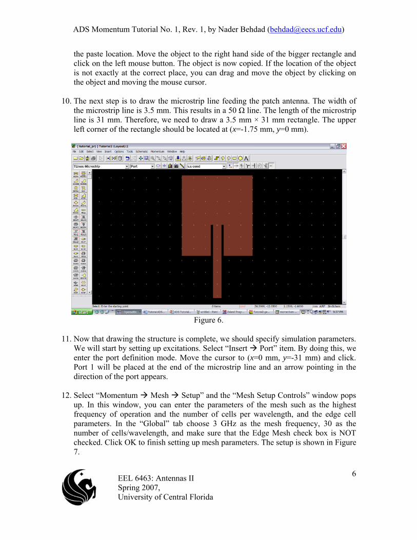
10. The next step is to draw the microstrip line feeding the patch antenna. The width of
the microstrip line is 3.5 mm. This results in a 50 Ω line. The length of the microstrip line is 31 mm. Therefore, we need to draw a 3.5 mm × 31 mm rectangle. The upper left corner of the rectangle should be located at (x=-1.75 mm, y=0 mm).
Figure 6.
11. Now that drawing the structure is complete, we should specify simulation parameters.
We will start by setting up excitations. Select “Insert Port” item. By doing this, we enter the port definition mode. Move the cursor to (x=0 mm, y=-31 mm) and click. Port 1 will be placed at the end of the microstrip line and an arrow pointing in the direction of the port appears.
12. Select “Momentum Mesh Setup” and the “Mesh Setup Controls” window pops
up. In this window, you can enter the parameters of the mesh such as the highest frequency of operation and the number of cells per wavelength, and the edge cell parameters. In the “Global” tab choose 3 GHz as the mesh frequency, 30 as the number of cells/wavelength, and make sure that the Edge Mesh check box is NOT checked. Click OK to finish setting up mesh parameters. The setup is shown in Figure 7.

ADS Momentum Tutorial No. 1, Rev. 1, by Nader Behdad ([email protected])
EEL 6463: Antennas II Spring 2007, University of Central Florida
7
Figure 7.
13. Select “Momentum Mesh Precompute…”. The “Precompute Mesh” window
appears. Click OK and the mesh will be calculated and displayed. 14. Select the “Momentum Simulation S-parameters…”. The simulation control
menu pops up; in the “Edit/Define Frequency Plan” field, choose “Adaptive” from the “Sweep Type” menu. Enter 1 and 3 GHz in the Start and Stop frequency points and enter 201 as the “Sample Point Limits”. Click on “Add to Frequency Plan List” to add the sweep to the “Frequency Plans” list; make sure that the “Open data display when simulation completes” check box is checked. Click on Simulate to start simulating the structure. You can see the simulation progress in the momentum window as shown in Figure 8.
15. After the simulation is complete the display window opens and the program plots the
magnitude and phase of S11 on separate plots. Furthermore, the program plots S11 on a smith chart. Chose “Marker New…” in the Display Window and click on one of the curves. ADS inserts a marker on the appropriate curve and you can move the marker by dragging it and moving your mouse cursor.
16. The next step is to calculate the current distribution on the surface of the antenna as
well as its radiation pattern and parameters. However, before that, we will repeat the simulation after increasing the number of cells from 30 Cells/λ to 70 Cells/λ and we will use Edge Cells; Select “Momentum Mesh Setup…” and enter the new

ADS Momentum Tutorial No. 1, Rev. 1, by Nader Behdad ([email protected])
EEL 6463: Antennas II Spring 2007, University of Central Florida
8
meshing information in the setup window and make sure the edge cell check box is checked. Then click OK;
Figure 8.
Figure 9.

ADS Momentum Tutorial No. 1, Rev. 1, by Nader Behdad ([email protected])
EEL 6463: Antennas II Spring 2007, University of Central Florida
9
17. Select “Momentum Mesh Precompute …” to see the new meshed structure. After this, simulate the structure by selecting “Momentum Simulation S-Parameters…”. This time, it will take much longer to simulate the structure. Increasing the number of cells increases the time and memory required to complete the MoM simulation.
18. After the simulation is completed, go to the Display Window and place a marker on
the S11 trace to find the center frequency of operation. Once you locate this center frequency of operation, you can simulate the structure at this frequency to calculate the current distribution over the surface of the antenna and its feeding structure. The new S11 response is shown in Figure 10; as the marker indicates, the center frequency of operation is at 2.395 GHz; simulate the structure, this time only at 2.395 GHz
1.5 2.0 2.51.0 3.0
-10
-8
-6
-4
-2
-12
0
Frequency
Mag
. [d
B]
m1
S11
m1freq=dB(Tutorial2_mom_a..S(1,1))=-11.765
2.395GHz
Figure 10.
19. After the simulation is complete, select “Momentum Post Processing
Visualization…”. The Momenum Visualization window pops up. In this window, you can view the current distribution over the surface of the antenna in different formats.
20. In the Momentum Visualization window, select “Current Set Port Solution
Weights …”. Enter 1 as the Solution Weight and 90 as the Solution Phase. Clock OK. Select “Current Plot Currents …”. You can choose the different current parameters in this menu and plot the surface current on the surface of the antenna.
21. In the Momentum Visualization window, there are a number of other options that you
can change. You can choose to view the current animation by using the controls located on the left hand side of screen

ADS Momentum Tutorial No. 1, Rev. 1, by Nader Behdad ([email protected])
EEL 6463: Antennas II Spring 2007, University of Central Florida
10
Figure 11.
22. In the Momentum Layout view, select “Momentum Post Processing Radiation
Pattern…”. The “Radiation Pattern Control” menu pops up and you can enter the pattern information in this window. Under the “General” tab, choose “3D Visualization” Radio button under the “Visualization Type” field and click on “Continue” button to calculate the radiation pattern.
23. After the pattern calculation is complete, Momentum automatically invokes the
“Momentum Visualization” window. Notice that the new menu item “Far Field” is added now.
24. Select “Far Field Far Field Plot …”. Do not change anything in the new menu that
pops up. Click OK and the 3D radiation plot will be plotted in the Visualization window. This three-dimensional radiation pattern is shown in Figure 12; if you want to draw the 2D pattern, you can plot it from the “far-field” menu of the Momentum “Visualization Window”. Select “Far Field Cut 3D far field…” and a new window pops up in which you can choose the 2D cut planes. Choose phi cut and chose a constant phi value of 0 degrees, then press apply. Then choose the phi value of 90 degrees and press apply again. Now, you have selected the 2D cuts of the 3D pattern that correspond to the E-plane and H-plane of the microstrip patch antenna.
25. Now, select “Fari Field Plot Far Field Cut …” and a new window pops up. In this
new window, you can choose the cuts specified in the previous step and plot them easily. Select the two plots listed under “2D far field Plots” field and press the apply button located on the lower side of the window. The 2D cuts will be plotted in a new pattern plot. This plot is shown in Figure 13.

ADS Momentum Tutorial No. 1, Rev. 1, by Nader Behdad ([email protected])
EEL 6463: Antennas II Spring 2007, University of Central Florida
11
Figure 12.
Figure 13.

ADS Momentum Tutorial No. 1, Rev. 1, by Nader Behdad ([email protected])
EEL 6463: Antennas II Spring 2007, University of Central Florida
12
26. In the “Momentum Visualization Window” you can also check the radiation parameters of the antenna. Select “Far Field Antenna parameters …” item and a window pops up in which the radiation parameters of the antenna such as its gain, efficiency, and directivity are listed in different fields.

专注于微波、射频、天线设计人才的培养 易迪拓培训 网址:http://www.edatop.com
射 频 和 天 线 设 计 培 训 课 程 推 荐
易迪拓培训(www.edatop.com)由数名来自于研发第一线的资深工程师发起成立,致力并专注于微
波、射频、天线设计研发人才的培养;我们于 2006 年整合合并微波 EDA 网(www.mweda.com),现
已发展成为国内最大的微波射频和天线设计人才培养基地,成功推出多套微波射频以及天线设计经典
培训课程和 ADS、HFSS 等专业软件使用培训课程,广受客户好评;并先后与人民邮电出版社、电子
工业出版社合作出版了多本专业图书,帮助数万名工程师提升了专业技术能力。客户遍布中兴通讯、
研通高频、埃威航电、国人通信等多家国内知名公司,以及台湾工业技术研究院、永业科技、全一电
子等多家台湾地区企业。
易迪拓培训课程列表:http://www.edatop.com/peixun/rfe/129.html
射频工程师养成培训课程套装
该套装精选了射频专业基础培训课程、射频仿真设计培训课程和射频电
路测量培训课程三个类别共 30 门视频培训课程和 3 本图书教材;旨在
引领学员全面学习一个射频工程师需要熟悉、理解和掌握的专业知识和
研发设计能力。通过套装的学习,能够让学员完全达到和胜任一个合格
的射频工程师的要求…
课程网址:http://www.edatop.com/peixun/rfe/110.html
ADS 学习培训课程套装
该套装是迄今国内最全面、最权威的 ADS 培训教程,共包含 10 门 ADS
学习培训课程。课程是由具有多年 ADS 使用经验的微波射频与通信系
统设计领域资深专家讲解,并多结合设计实例,由浅入深、详细而又
全面地讲解了 ADS 在微波射频电路设计、通信系统设计和电磁仿真设
计方面的内容。能让您在最短的时间内学会使用 ADS,迅速提升个人技
术能力,把 ADS 真正应用到实际研发工作中去,成为 ADS 设计专家...
课程网址: http://www.edatop.com/peixun/ads/13.html
HFSS 学习培训课程套装
该套课程套装包含了本站全部 HFSS 培训课程,是迄今国内最全面、最
专业的HFSS培训教程套装,可以帮助您从零开始,全面深入学习HFSS
的各项功能和在多个方面的工程应用。购买套装,更可超值赠送 3 个月
免费学习答疑,随时解答您学习过程中遇到的棘手问题,让您的 HFSS
学习更加轻松顺畅…
课程网址:http://www.edatop.com/peixun/hfss/11.html
`

专注于微波、射频、天线设计人才的培养 易迪拓培训 网址:http://www.edatop.com
CST 学习培训课程套装
该培训套装由易迪拓培训联合微波 EDA 网共同推出,是最全面、系统、
专业的 CST 微波工作室培训课程套装,所有课程都由经验丰富的专家授
课,视频教学,可以帮助您从零开始,全面系统地学习 CST 微波工作的
各项功能及其在微波射频、天线设计等领域的设计应用。且购买该套装,
还可超值赠送 3 个月免费学习答疑…
课程网址:http://www.edatop.com/peixun/cst/24.html
HFSS 天线设计培训课程套装
套装包含 6 门视频课程和 1 本图书,课程从基础讲起,内容由浅入深,
理论介绍和实际操作讲解相结合,全面系统的讲解了 HFSS 天线设计的
全过程。是国内最全面、最专业的 HFSS 天线设计课程,可以帮助您快
速学习掌握如何使用 HFSS 设计天线,让天线设计不再难…
课程网址:http://www.edatop.com/peixun/hfss/122.html
13.56MHz NFC/RFID 线圈天线设计培训课程套装
套装包含 4 门视频培训课程,培训将 13.56MHz 线圈天线设计原理和仿
真设计实践相结合,全面系统地讲解了 13.56MHz线圈天线的工作原理、
设计方法、设计考量以及使用 HFSS 和 CST 仿真分析线圈天线的具体
操作,同时还介绍了 13.56MHz 线圈天线匹配电路的设计和调试。通过
该套课程的学习,可以帮助您快速学习掌握 13.56MHz 线圈天线及其匹
配电路的原理、设计和调试…
详情浏览:http://www.edatop.com/peixun/antenna/116.html
我们的课程优势:
※ 成立于 2004 年,10 多年丰富的行业经验,
※ 一直致力并专注于微波射频和天线设计工程师的培养,更了解该行业对人才的要求
※ 经验丰富的一线资深工程师讲授,结合实际工程案例,直观、实用、易学
联系我们:
※ 易迪拓培训官网:http://www.edatop.com
※ 微波 EDA 网:http://www.mweda.com
※ 官方淘宝店:http://shop36920890.taobao.com
专注于微波、射频、天线设计人才的培养
官方网址:http://www.edatop.com 易迪拓培训 淘宝网店:http://shop36920890.taobao.com