amis-30624 - i 2 c micro-stepping motor driver
TRANSCRIPT

Semiconductor Components Industries, LLC, 2009
September, 2009 − Rev. 51 Publication Order Number:
AMIS−30624/D
AMIS-30624, NCV70624
I2C Micro-stepping MotorDriver
INTRODUCTIONThe AMIS−30624/NCV70624 is a single−chip micro−stepping
motor driver with a position controller and control/diagnosticinterface. It is ready to build intelligent peripheral systems where up to32 drivers can be connected to one I2C master. This significantlyreduces system complexity.
The chip receives positioning instructions through the bus andsubsequently drives the stator coils so the two−phase stepper motormoves to the desired position. The on−chip position controller isconfigurable (OTP or RAM) for different motor types, positioningranges and parameters for speed, acceleration and deceleration.Micro−stepping allows silent motor operation and increasedpositioning resolution. The advanced motion qualification modeenables verification of the complete mechanical system in function ofthe selected motion parameters. The AMIS−30624/NCV70624 caneasily be connected to an I2C bus where the I2C master can fetchspecific status information like actual position, error flags, etc. fromeach individual slave node.
An integrated sensorless step−loss detection prevents the positionerfrom loosing steps and stops the motor when running into stall. Thisenables silent, yet accurate position calibrations during a referencingrun and allows semi−closed loop operation when approaching themechanical end−stops.
The chip is implemented in I2T100 technology, enabling both highvoltage analog circuitry and digital functionality on the same chip.The NCV70624 is fully compatible with the automotive voltagerequirements.
PRODUCT FEATURESMotor Driver Micro−Stepping Technology
Sensorless Step−Loss Detection
Peak Current Up to 800 mA
Fixed Frequency PWM Current−Control
Selectable PWM Frequency
Automatic Selection of Fast and Slow Decay Mode
No external Fly−back Diodes Required
14 V/24 V Compliant
Motion Qualification Mode (Note 1)
Controller with RAM and OTP Memory Position Controller
Configurable Speeds and Acceleration
Input to Connect Optional Motion Switch
I2C Interface Bi−Directional 2−Wire Bus for Inter IC Control
Field Programmable Node Addresses
Full Diagnostics and Status Information
Protection Overcurrent Protection
Undervoltage Management
Open−circuit Detection
High Temperature Warning and Management
Low Temperature Flag
EMI Compatibility High Voltage Outputs with Slope Control
Patents US 7,271,993
US 7,288,956
This is a Pb−Free Device
NCV Prefix for Automotive and Other ApplicationsRequiring Site and Control Changes
1. Not applicable for “Product Versions NCV70624DW010G, NCV70624DW010R2G”
http://onsemi.com
See detailed ordering and shipping information in the packagedimensions section on page 2 of this data sheet.
ORDERING INFORMATION
SOIC−204 or DW010 SUFFIX
CASE 751AQ
NQFP−325 SUFFIX
CASE 560AA

AMIS−30624, NCV70624
http://onsemi.com2
APPLICATIONS
The AMIS−30624/NCV70624 is ideally suited for smallpositioning applications. Target markets include:automotive (headlamp alignment, HVAC, idle control,cruise control), industrial equipment (lighting, fluid control,labeling, process control, XYZ tables, robots) and building
automation (HVAC, surveillance, satellite dish, renewableenergy systems). Suitable applications typically havemultiple axes or require mechatronic solutions with thedriver chip mounted directly on the motor.
Table 1. ORDERING INFORMATION
Part No. Peak Current End Market/Version Package* Shipping†
AMIS30624C6244G 800 mA
IndustrialHigh Voltage Version
SOIC−20(Pb−Free)
Tube/Tray
AMIS30624C6244RG 800 mA SOIC−20(Pb−Free)
Tape & Reel
AMIS30624C6245G 800 mA NQFP−32 (7 x 7 mm)(Pb−Free)
Tube/Tray
AMIS30624C6245RG 800 mA NQFP−32 (7 x 7 mm)(Pb−Free)
Tape & Reel
NCV70624DW010G 800 mAAutomotive
High TemperatureVersion
SOIC−20(Pb−Free)
Tube/Tray
NCV70624DW010R2G 800 mA SOIC−20(Pb−Free)
Tape & Reel
*For additional information on our Pb−Free strategy and soldering details, please download the ON Semiconductor Soldering and MountingTechniques Reference Manual, SOLDERRM/D.
†For information on tape and reel specifications, including part orientation and tape sizes, please refer to our Tape and Reel PackagingSpecification Brochure, BRD8011/D.
QUICK REFERENCE DATA
Table 2. ABSOLUTE MAXIMUM RATINGS
Parameter Min Max Unit
VBB, VHW, VSWI Supply voltage, hardwired address and SWI pins −0.3 +40 (Note 2) V
TJ Junction temperature range (Note 3) −50 +175 C
Tst Storage temperature −55 +160 C
Vesd (Note 4) Human Body Model (HBM) Electrostatic discharge voltage on pins −2 +2 kV
Machine Model (MM) Electrostatic discharge voltage on pins −200 +200 V
Stresses exceeding Maximum Ratings may damage the device. Maximum Ratings are stress ratings only. Functional operation above theRecommended Operating Conditions is not implied. Extended exposure to stresses above the Recommended Operating Conditions may affectdevice reliability.2. For limited time: VBB < 0.5 s, SWI and HW pins <1.0 s.3. The circuit functionality is not guaranteed.4. HBM according to AEC−Q100: EIA−JESD22−A114−B (100 pF via 1.5 k�) and MM according to AEC−Q100: EIA−JESD22−A115−A.
Table 3. OPERATING RANGES
Parameter Min Max Unit
VBB Supply voltage +6.5 +29 V
TJ Operating temperature range −40 +165 C
AMIS−30624, NCV70624
http://onsemi.com3
Table of ContentsGeneral Description 1. . . . . . . . . . . . . . . . . . . . . . . . . . . .Product Features 1. . . . . . . . . . . . . . . . . . . . . . . . . . . . . .Applications 2. . . . . . . . . . . . . . . . . . . . . . . . . . . . . . . . . .Ordering Information 2. . . . . . . . . . . . . . . . . . . . . . . . . . .Quick Reference Data 2. . . . . . . . . . . . . . . . . . . . . . . . . .Maximum Ratings 2. . . . . . . . . . . . . . . . . . . . . . . . . . . . .Block Diagram 3. . . . . . . . . . . . . . . . . . . . . . . . . . . . . . . .Pin Description 4. . . . . . . . . . . . . . . . . . . . . . . . . . . . . . .Package Thermal Resistance 5. . . . . . . . . . . . . . . . . . . . .DC Parameters 6. . . . . . . . . . . . . . . . . . . . . . . . . . . . . . . .AC Parameters 8. . . . . . . . . . . . . . . . . . . . . . . . . . . . . . . .Typical Application 10. . . . . . . . . . . . . . . . . . . . . . . . . . .
Positioning Parameters 11. . . . . . . . . . . . . . . . . . . . . . . . .Structural Description 14. . . . . . . . . . . . . . . . . . . . . . . . .Functions Description 15. . . . . . . . . . . . . . . . . . . . . . . . .Position Controller 15. . . . . . . . . . . . . . . . . . . . . . . . . . . .Main Control and Register 22. . . . . . . . . . . . . . . . . . . . . .Autarkic Functionality in Undervoltage Condition 24. . .OTP Register 25. . . . . . . . . . . . . . . . . . . . . . . . . . . . . . . .Priority Encoder 30. . . . . . . . . . . . . . . . . . . . . . . . . . . . . .Motordriver 32. . . . . . . . . . . . . . . . . . . . . . . . . . . . . . . . .I2C Bus Description 37. . . . . . . . . . . . . . . . . . . . . . . . . . .I2C Application Commands 42. . . . . . . . . . . . . . . . . . . . .Package Outlines 50. . . . . . . . . . . . . . . . . . . . . . . . . . . . .
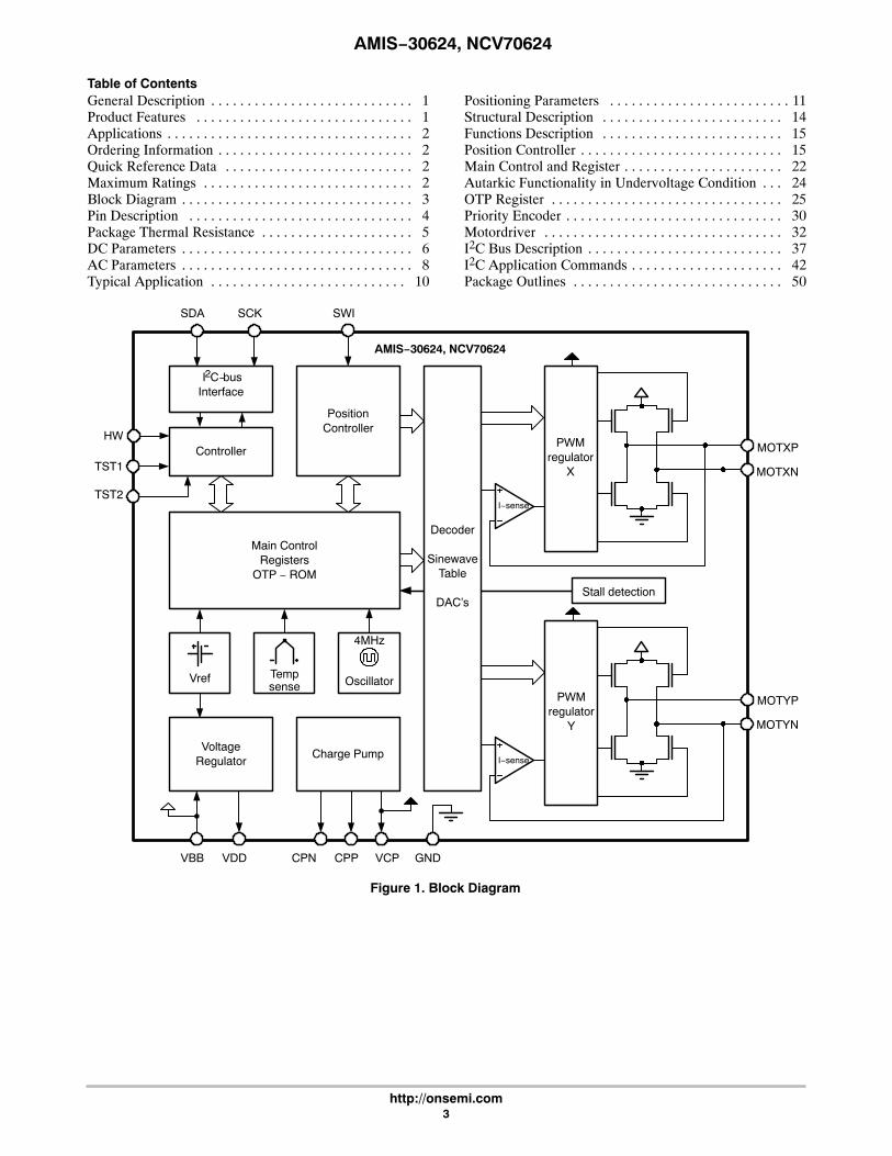
Figure 1. Block Diagram
I2C−busInterface
OscillatorVref Tempsense
VoltageRegulator
TST2
VBB VDD GND
MOTXP
MOTXN
Main ControlRegisters
OTP − ROM
4MHz
Charge Pump
CPN CPP VCP
Stall detection
PositionController
ControllerTST1
MOTYP
MOTYN
PWMregulator
Y
PWMregulator
X
I−sense
Decoder
SinewaveTable
DAC’s
AMIS−30624, NCV70624
HW
SWISDA SCK
I−sense
AMIS−30624, NCV70624
http://onsemi.com4
1
2
3
5
4
6
7
8
24
23
22
20
21
19
18
17
9
10 11 12 13 14 15
16
32
31 30 29 28 27 26
25
XP
VBB
SWI
NC
SDA
XP
VBB
VBB
CPN
CPP
VCP
YN
VBB
YN
VBB
VBB
YP
XN
GN
D
GN
D
XN
YP
GN
D
GN
D
SC
K
VD
D
GN
D
TS
T1
TS
T2
HW
GN
D
NC
AMIS−3062417
18
19
201
2
3
4
SDA
GND
SWI
GND
SCK
MOTXP
VBB
VDD
16
15
14
13
12
11
5
6
7
8
9
10
GND GND
MOTXN
MOTYP
MOTYN
TST1
TST2
HW
CPN
CPP
VBB
VCP
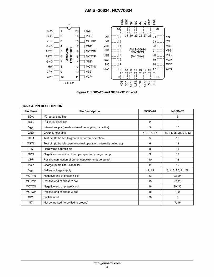
SOIC−20
Figure 2. SOIC−20 and NQFP−32 Pin−out
AM
IS−30624
(Top View)
NC
V70624
NCV70624
Table 4. PIN DESCRIPTION
Pin Name Pin Description SOIC−20 NQFP−32
SDA I2C serial data line 1 8
SCK I2C serial clock line 2 9
VDD Internal supply (needs external decoupling capacitor) 3 10
GND Ground, heat sink 4, 7, 14, 17 11, 14, 25, 26, 31, 32
TST1 Test pin (to be tied to ground in normal operation) 5 12
TST2 Test pin (to be left open in normal operation: internally pulled up) 6 13
HW Hard wired address bit 8 15
CPN Negative connection of pump−capacitor (charge pump) 9 17
CPP Positive connection of pump−capacitor (charge pump) 10 18
VCP Charge−pump filter−capacitor 11 19
VBB Battery voltage supply 12, 19 3, 4, 5, 20, 21, 22
MOTYN Negative end of phase Y coil 13 23, 24
MOTYP Positive end of phase Y coil 15 27, 28
MOTXN Negative end of phase X coil 16 29, 30
MOTXP Positive end of phase X coil 18 1, 2
SWI Switch input 20 6
NC Not connected (to be tied to ground) 7, 16

AMIS−30624, NCV70624
http://onsemi.com5
PACKAGE THERMAL RESISTANCE
The AMIS−30624/NCV70624 is available in SOIC−20 oroptimized NQFP−32 packages. For cooling optimizations,the NQFP has an exposed thermal pad which has to besoldered to the PCB ground plane. The ground plane needsthermal vias to conduct the head to the bottom layer. Figures3 and 4 give examples for good power distribution solutions.
For precise thermal cooling calculations the majorthermal resistances of the devices are given. The thermalmedia to which the power of the devices has to be given are: Static environmental air (via the case)
PCB board copper area (via the device pins andexposed pad)The thermal resistances are presented in Table 5: DC
Parameters.
The major thermal resistances of the device are the Rthfrom the junction to the ambient (Rthja) and the overall Rthfrom the junction to the leads (Rthjp).
The NQFP device is designed to provide superior thermalperformance. Using an exposed die pad on the bottomsurface of the package is mainly contributing to thisperformance. In order to take full advantage of the exposedpad, it is most important that the PCB has features to conductheat away from the package. A thermal grounded pad withthermal vias can achieve this.
In the table below, one can find the values for the Rthja andRthjp, simulated according to the JESD−51 norm:
Package
RthJunction−to−Leads and
Exposed Pad − Rthjp
RthJunction−to−Leads
Rthjp
RthJunction−to−Ambient
Rthja (1S0P)
RthJunction−to−Ambient
Rthja (2S2P)
SOIC−20 19 62 39
NQFP−32 0,95 60 30
The Rthja for 2S2P is simulated conform to JESD−51 asfollows: A 4−layer printed circuit board with inner power planes
and outer (top and bottom) signal layers is used Board thickness is 1.46 mm (FR4 PCB material)
The 2 signal layers: 70 �m thick copper with an area of5500 mm2 copper and 20% conductivity
The 2 power internal planes: 36 �m thick copper withan area of 5500 mm2 copper and 90% conductivity
The Rthja for 1S0P is simulated conform to JESD−51 asfollows: A 1−layer printed circuit board with only 1 layer
Board thickness is 1.46 mm (FR4 PCB material)
The layer has a thickness of 70 �m copper with an areaof 5500 mm2 copper and 20% conductivity
ÎÎÎÎÎÎÎÎÎÎÎÎÎÎÎÎÎÎÎÎÎÎÎÎÎÎÎÎÎÎÎÎÎÎÎÎÎÎÎÎÎÎÎÎÎÎÎÎÎÎÎÎÎÎÎÎÎÎÎÎÎÎÎÎÎÎÎÎÎÎÎÎÎÎÎÎÎÎÎÎÎÎÎÎÎÎÎÎÎÎÎ
ÏÏÏÏÏÏ
ÎÎÎÎÎÎÎÎÎÎÎÎÎÎÎÎÎÎÎÎÎÎÎÎÎÎÎÎÎÎÎÎÎÎÎÎÎÎÎÎÎÎÎÎÎÎÎÎÎÎÎÎÎÎÎÎÎÎÎÎÎÎÎÎÎÎÎÎÎÎÎÎÎÎÎÎÎÎÎÎÎÎÎÎ
Figure 3. Example of SOIC−20 PCB Ground PlaneLayout (preferred layout at top and bottom)
Figure 4. Example of NQFP−32 PCB Ground PlaneLayout (preferred layout at top and bottom)
NQFP−32
SO
IC−20

AMIS−30624, NCV70624
http://onsemi.com6
DC PARAMETERS
The DC parameters are guaranteed overtemperature and VBB in the operating range, unless otherwise specified. Convention:currents flowing into the circuit are defined as positive.
Table 5. DC PARAMETERS
Symbol Pin(s) Parameter Test Conditions Min Typ Max Unit
MOTORDRIVER
IMSmax,Peak
MOTXPMOTXNMOTYPMOTYN
Max current through motor coilin normal operation
VBB = 14 V 800 mA
IMSmax,RMS Max rms current through coil innormal operation
VBB = 14 V 570 mA
IMSabs Absolute error on coilcurrent (Note 5)
VBB = 14 V −10 10 %
IMSrel Matching of X & Ycoil currents
VBB = 14 V −7 0 7 %
RDS(on) On resistance for eachmotor pin at IMSmax(Note 6)
VBB = 12 V, Tj = 50C 0.50 1 �
VBB = 8 V, Tj = 50C 0.55 1 �
VBB = 12 V, Tj = 150C 0.70 1 �
VBB = 8 V, Tj = 150C 0.85 1 �
IMSL Pulldown current HiZ mode, VBB = 7.8 V 2 mA
I2C SERIAL INTERFACE
VIL
SDASCK
Input level low (Note 11) −0.5 0.3 * VDD V
VIH Input level high (Note 12) 0.7 * VDD VDD + 0.5 V
VnL Noise margin at the LOW levelfor each connected device(including hysteresis)
0.1 * VDD V
VnH Noise margin at the HIGH levelfor each connected device(including hysteresis)
0.2 * VDD
THERMAL WARNING & SHUTDOWN
Ttw Thermal warning(Notes 7 and 8)
138 145 152 C
Ttsd Thermal shutdown (Note 9) Ttw + 10 C
Tlow Low temperature warning (Note9)
Ttw − 155 C
SUPPLY AND VOLTAGE REGULATOR
VbbOTP
VBB
Supply voltage for OTPzapping (Note 10)
9.0 10.0 V
UV1 Stop voltage high threshold 7.8 8.4 8.9 V
UV2 Stop voltage low threshold 7.1 7.5 8.0 V
Ibat Total current consumption Unloaded outputsVBB = 29 V
3.50 10.0 mA
5. Tested in production for 800 mA, 400 mA, 200 mA and 100 mA current settings for both X and Y coil.6. Not measured in production. Guaranteed by design.7. Parameter guaranteed by trimming relevant OTP’s in production test at 143C (5C) and VBB = 14 V.8. No more than 100 cumulated hours in life time above Tw.9. Thermal shutdown and low temperature warning are derived from thermal warning. Guaranteed by design.10.A buffer capacitor of minimum 100 �F is needed between VBB and GND. Short connections to the power supply are recommended.11. If input voltages < − 0.3 V, than a resistor between 22 � to 100 � needs to be put in series.12. If the I2C−bus is operated in Fast Mode VIHmin = 0.7 * VDD.

AMIS−30624, NCV70624
http://onsemi.com7
Table 5. DC PARAMETERS
Symbol Pin(s) Parameter Test Conditions Min Typ Max Unit
SUPPLY AND VOLTAGE REGULATOR
VDD
VDD
Regulated internal supply(Note 13)
8 V < VBB < 29 V 4.75 5 5.50 V
VddReset Digital supply reset level @power down (Note 14)
4.5 V
IddLim Current limitation Pin shorted to groundVBB = 14 V
45 mA
SWITCH INPUT AND HARDWIRE ADDRESS INPUT
Rt_OFF
SWI HW
Switch OPEN resistance(Note 15)
10 k�
Rt_ON Switch ON resistance(Note 15)
Switch to GND or VBB 2 k�
Vbb_sw VBB range for guaranteedoperation of SWI and HW
6 29 V
Ilim_sw Current limitation Short to GND or Vbat
VBB = 29 V20 30 45 mA
TEST PIN
Vihigh
TST
Input level high VBB = 14 V 0.7 * Vdd V
Vilow Input level low VBB = 14 V 0.3 * Vdd V
HWhyst Hysteresis VBB = 14 V 0.075 * Vdd V
CHARGE PUMP
Vcp
VCP
Output voltage 6 V VBB 14 V 2 * VBB − 2.5 V
14 V VBB 30 V VBB + 10 VBB + 15 V
Cbuffer External buffer capacitor 220 470 nF
Cpump CPPCPN
External pump capacitor 220 470 nF
MOTION QUALIFICATION MODE OUTPUT (Note 16)
VOUT
SWI
Output voltage swing TestBemf I2C command 0 − 4,85 V
ROUT Output impedance Service mode I2C command 2 k�
Av Gain = VSWI / VBEMF Service mode I2C command 0.50
PACKAGE THERMAL RESISTANCE VALUES
Rthja SOThermal resistance junctionto ambient (2S2P)
Simulated conformJEDEC JESD51
39 K/W
Rthjp SOThermal resistance junctionto leads
19 K/W
Rthja NQThermal resistance junctionto ambient (2S2P)
30 K/W
Rthjp NQThermal resistance junctionto leads and exposed pad
0.95 K/W
13.Pin VDD must not be used for any external supply14.The RAM content will not be altered above this voltage.15.External resistance value seen from pin SWI or HW, including 1 k� series resistor. For the switch OPEN, the maximum allowed leakage
current is represented by a minimum resistance seen from the pin.16.Not applicable for “Product Versions NCV70624DW010G, NCV70624DW010R2G”

AMIS−30624, NCV70624
http://onsemi.com8
AC PARAMETERS
The AC parameters are guaranteed for temperature and VBB in the operating range unless otherwise specified.
Table 6. AC PARAMETERS
Symbol Pin(s) Parameter Test Conditions Min Typ Max Unit
POWERUP
Tpu Power−up time Guaranteed by design 10 ms
INTERNAL OSCILLATOR
fosc Frequency of internal oscillator VBB = 14 V 3.6 4.0 4.4 MHz
I2C TRANSCEIVER (STANDARD MODE)
fSCL
SDASCK
SCL clock frequency 100 kHz
tHD,START Hold time (repeated) START condition. Afterthis period the first clock pulse is generated.
4.0 �s
tLOW LOW period of the SCK clock 4.7 �s
tHIGH HIGH period of the SCK clock 4.0 �s
tSU,START Set−up time for a repeated START condition 4.7 �s
tHD,DATA Data hold time for I2C bus devices 0(Note 18)
3.45(Note 19)
�s
tSU,DATA Data set−up time 250 ns
tR Rise time of SDA and SCK signals 1.0 �s
tF Fall time of SDA and SCK signals 0.3 �s
tSU,STOP Set−up time for STOP condition 4.0 �s
tBUF Bus free time between STOP and STARTcondition
4.7 �s
I2C TRANSCEIVER (FAST MODE)
fSCL
SDASCK
SCL clock frequency 360 kHz
tHD,START Hold time (repeated) START condition. Afterthis period the first clock pulse is generated.
0.6 �s
tLOW LOW period of the SCK clock 1.3 �s
tHIGH HIGH period of the SCK clock 0.6 �s
tSU,START Set−up time for a repeated START condition 0.6 �s
tHD,DATA Data hold time for I2C bus devices 0(Note 18)
0.9(Note 19)
�s
tSU,DATA Data set−up time 100(Note 20)
ns
tR Rise time of SDA and SCK signals 20 +0.1 CB
300 ns
tF Fall time of SDA and SCK signals 20 +0.1 CB
300 ns
tSU,STOP Set−up time for STOP condition 0.6 �s
tBUF Bus free time between STOP and STARTcondition
1.3 �s
17.The maximum number of connected I2C devices is dependent on the number of available addresses and the maximum bus capacitanceto still guarantee the rise and fall times of the bus signals.
18.An I2C device must internally provide a hold time of at least 300 ns for the SDA signal (referred to the VIHmin of the SCL signal) to bridgethe undefined region of the falling edge of SCL.
19.The maximum tHD,DAT has only to be met if the device does not stretch the LOW period (tLOW) of the SCL signal.20.A Fast−mode I2C−bus device can be used in a standard−mode I2C bus system, but the requirement tSU,DATA � 250 ns must than be met.
This will automatically be the case if the device does not stretch the LOW period of the SCL signal. If such a device does stretch the LOWperiod of the SCL signal, it must output the next data bit to the SDA line trmax + tSU,DATA = 1000 + 250 = 1250 ns (according to thestandard−mode I2C−bus specification) before the SCL line is released.

AMIS−30624, NCV70624
http://onsemi.com9
Table 6. AC PARAMETERS
Symbol UnitMaxTypMinTest ConditionsParameterPin(s)
SWITCH INPUT AND HARDWIRE ADDRESS INPUT
TswSWIHW
Scan pulse period (Note 21) VBB = 14 V 1024 �s
Tsw_on Scan pulse duration(Note 21)
VBB = 14 V 128 �s
MOTORDRIVER
Fpwm
MOTxx
PWM frequency (Note 21) PWMfreq = 0 (Note 22) 20.6 22.8 25.0 kHz
PWMfreq = 1 (Note 22) 41.2 45.6 50.0 kHz
Fjit_depth PWM jitter modulation depth PWMJen = 1 (Note 22) 10 %
Tbrise Turn−on transient time Between 10% and 90% 140 ns
Tbfall Turn−off transient time 130 ns
Tstab Run current stabilization time (Note 21) 29 32 35 ms
CHARGE PUMP
fCP CPNCPP
Charge pump frequency(Note 21)
VBB = 14 V 250 kHz
21.Derived from the internal oscillator22.See SetMotorParam and PWM Regulator
Figure 5. I2C Timing Diagrams
SDA
SCK
tF
tHD,START
tLOW
tR
tHD,DATA
tSU,DATA
tHIGH
START REPEATED START
tSU,START tSP tSU,STOP
tBUF
STARTSTOP
VIHmin
VILmax

AMIS−30624, NCV70624
http://onsemi.com10
Typical Application
AMIS−30624,
GND
2
MOTXP
TST2
100 nF
2,7 nF
MOTXN
MOTYP
MOTYN
11VDD
VBB
12
VCP
SWI
CPPCPN
9
8
SDA
SCK
10
HW
18
M
16
15
13
20
TST1
3
VBB
19
1
65 4 7 14 17
100 nF220 nF
2,7 nF
1 k
1 k
Figure 6. Typical Application Diagram for SO Device
VBAT
C8
C1
Connectto VBATor GND
C7
100 �F
C2
Connectto VBATor GND
C4
100 nF
C3
C5
C6 220 nF
NCV70624
I2C Bus
NOTES: All resistors are 5%, 1/4 W C1, C2 minimum value is 2.7 nF, maximum value is 10 nFDepending on the application, the ESR value and working voltage of C7 must be carefully chosenC3 and C4 must be close to pins VBB and GNDC5 and C6 must be as close as possible to pins CPN, CPP, VCP, and VBB to reduce EMC radiationC9 must be a ceramic capacitor to assure low ESR
AMIS−30624, NCV70624
http://onsemi.com11
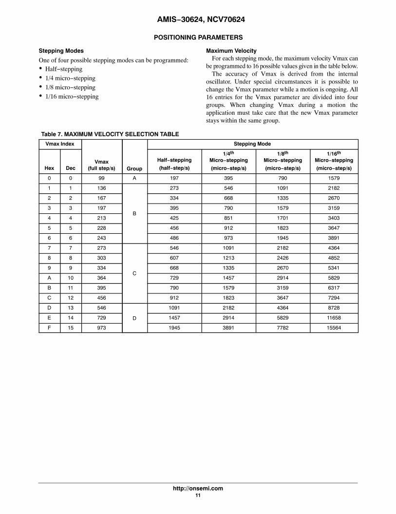
POSITIONING PARAMETERS
Stepping Modes
One of four possible stepping modes can be programmed: Half−stepping
1/4 micro−stepping
1/8 micro−stepping
1/16 micro−stepping
Maximum VelocityFor each stepping mode, the maximum velocity Vmax can
be programmed to 16 possible values given in the table below.The accuracy of Vmax is derived from the internal
oscillator. Under special circumstances it is possible tochange the Vmax parameter while a motion is ongoing. All16 entries for the Vmax parameter are divided into fourgroups. When changing Vmax during a motion theapplication must take care that the new Vmax parameterstays within the same group.
Table 7. MAXIMUM VELOCITY SELECTION TABLE
Vmax Index
Vmax(full step/s) Group
Stepping Mode
Hex Dec
Half−stepping
(half−step/s)
1/4th
Micro−stepping
(micro−step/s)
1/8th
Micro−stepping
(micro−step/s)
1/16th
Micro−stepping
(micro−step/s)
0 0 99 A 197 395 790 1579
1 1 136
B
273 546 1091 2182
2 2 167 334 668 1335 2670
3 3 197 395 790 1579 3159
4 4 213 425 851 1701 3403
5 5 228 456 912 1823 3647
6 6 243 486 973 1945 3891
7 7 273
C
546 1091 2182 4364
8 8 303 607 1213 2426 4852
9 9 334 668 1335 2670 5341
A 10 364 729 1457 2914 5829
B 11 395 790 1579 3159 6317
C 12 456 912 1823 3647 7294
D 13 546
D
1091 2182 4364 8728
E 14 729 1457 2914 5829 11658
F 15 973 1945 3891 7782 15564

AMIS−30624, NCV70624
http://onsemi.com12
Minimum VelocityOnce the maximum velocity is chosen, 16 possible values can be programmed for the minimum velocity Vmin. The table
below provides the obtainable values in full−step/s. The accuracy of Vmin is derived from the internal oscillator.
Table 8. OBTAINABLE VALUES IN FULL−STEP/s FOR THE MINIMUM VELOCITY
Vmin IndexVmaxFactor
Vmax (Full−step/s)
A B C D
Hex Dec 99 136 167 197 213 228 243 273 303 334 364 395 456 546 729 973
0 0 1 99 136 167 197 213 228 243 273 303 334 364 395 456 546 729 973
1 1 1/32 3 4 5 6 6 7 7 8 8 10 10 11 13 15 19 27
2 2 2/32 6 8 10 11 12 13 14 15 17 19 21 23 27 31 42 57
3 3 3/32 9 12 15 18 19 21 22 25 27 31 32 36 42 50 65 88
4 4 4/32 12 16 20 24 26 28 30 32 36 40 44 48 55 65 88 118
5 5 5/32 15 21 26 31 32 35 37 42 46 51 55 61 71 84 111 149
6 6 6/32 18 25 31 36 39 42 45 50 55 61 67 72 84 99 134 179
7 7 7/32 21 30 36 43 46 50 52 59 65 72 78 86 99 118 156 210
8 8 8/32 24 33 41 49 52 56 60 67 74 82 90 97 113 134 179 240
9 9 9/32 28 38 47 55 59 64 68 76 84 93 101 111 128 153 202 271
A 10 10/32 31 42 51 61 66 71 75 84 93 103 113 122 141 168 225 301
B 11 11/32 34 47 57 68 72 78 83 93 103 114 124 135 156 187 248 332
C 12 12/32 37 51 62 73 79 85 91 101 113 124 135 147 170 202 271 362
D 13 13/32 40 55 68 80 86 93 98 111 122 135 147 160 185 221 294 393
E 14 14/32 43 59 72 86 93 99 106 118 132 145 158 172 198 237 317 423
F 15 15/32 46 64 78 93 99 107 113 128 141 156 170 185 214 256 340 454
NOTES: The Vmax factor is an approximation.In case of motion without acceleration (AccShape = 1) the length of the steps = 1/Vmin. In case of accelerated motion(AccShape = 0) the length of the first step is shorter than 1/Vmin depending of Vmin, Vmax and Acc.
AMIS−30624, NCV70624
http://onsemi.com13
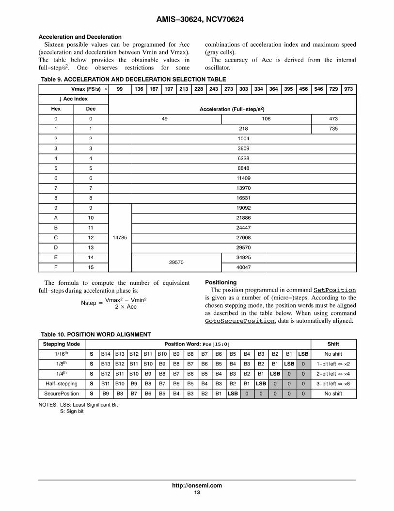
Acceleration and DecelerationSixteen possible values can be programmed for Acc
(acceleration and deceleration between Vmin and Vmax).The table below provides the obtainable values infull−step/s2. One observes restrictions for some
combinations of acceleration index and maximum speed(gray cells).
The accuracy of Acc is derived from the internaloscillator.
Table 9. ACCELERATION AND DECELERATION SELECTION TABLE
Vmax (FS/s) � 99 136 167 197 213 228 243 273 303 334 364 395 456 546 729 973
� Acc Index
Acceleration (Full−step/s2)Hex Dec
0 0 49 106 473
1 1 218 735
2 2 1004
3 3 3609
4 4 6228
5 5 8848
6 6 11409
7 7 13970
8 8 16531
9 9
14785
19092
A 10 21886
B 11 24447
C 12 27008
D 13 29570
E 1429570
34925
F 15 40047
The formula to compute the number of equivalentfull−steps during acceleration phase is:
Nstep �Vmax2
� Vmin2
2 � Acc
PositioningThe position programmed in command SetPosition
is given as a number of (micro−)steps. According to thechosen stepping mode, the position words must be alignedas described in the table below. When using commandGotoSecurePosition, data is automatically aligned.
Table 10. POSITION WORD ALIGNMENT
Stepping Mode Position Word: Pos[15:0] Shift
1/16th S B14 B13 B12 B11 B10 B9 B8 B7 B6 B5 B4 B3 B2 B1 LSB No shift
1/8th S B13 B12 B11 B10 B9 B8 B7 B6 B5 B4 B3 B2 B1 LSB 0 1−bit left 2
1/4th S B12 B11 B10 B9 B8 B7 B6 B5 B4 B3 B2 B1 LSB 0 0 2−bit left 4
Half−stepping S B11 B10 B9 B8 B7 B6 B5 B4 B3 B2 B1 LSB 0 0 0 3−bit left 8
SecurePosition S B9 B8 B7 B6 B5 B4 B3 B2 B1 LSB 0 0 0 0 0 No shift
NOTES: LSB: Least Significant BitS: Sign bit

AMIS−30624, NCV70624
http://onsemi.com14
Position RangesA position is coded by using the binary two’s complement format. According to the positioning commands used and to the
chosen stepping mode, the position range will be as shown in the following table.
Table 11. POSITION RANGE
Command Stepping Mode Position Range Full Range Excursion Number of Bits
SetPosition
Half−stepping −4096 to +4095 8192 half−steps 13
1/4th micro−stepping −8192 to +8191 16384 micro−steps 14
1/8th micro−stepping −16384 to +16383 32768 micro−steps 15
1/16th micro−stepping −32768 to +32767 65536 micro−steps 16
When using the command SetPosition, althoughcoded on 16 bits, the position word will have to be shifted tothe left by a certain number of bits, according to the steppingmode.
Secure PositionA secure position can be programmed. It is coded in
11−bits, thus having a lower resolution than normalpositions, as shown in the following table. See alsocommand GotoSecurePosition.
Table 12. SECURE POSITION
Stepping Mode Secure Position Resolution
Half−stepping 4 half−steps
1/4th micro−stepping 8 micro−steps (1/4th)
1/8th micro−stepping 16 micro−steps (1/8th)
1/16th micro−stepping 32 micro−steps (1/16th)
ImportantNOTES: The secure position is disabled in case the programmed value is the reserved code “10000000000” (0x400 or most negative
position).The resolution of the secure position is limited to 9 bit at start−up. The OTP register is copied in RAM as illustrated below. TheRAM bits SecPos1 and SecPos0 are set to 0.
SecPos10 SecPos9 SecPos8 SecPos2 SecPos1 SecPos0
SecPos10 SecPos9 SecPos8 SecPos2
RAM
OTP
ShaftA shaft bit, which can be programmed in OTP or with
command SetMotorParam, defines whether a positivemotion is a clockwise (CW) or counter−clockwise rotation(CCW) (an outer or an inner motion for linear actuators):
Shaft = 0 MOTXP is used as positive pin of the Xcoil, while MOTXN is the negative one.
Shaft = 1 opposite situation
Exception: in RunVelocity mode, the shaft bit has nofunction. In this mode the rotational direction is always CWor CCW, which is only determined by the motor wiring.
STRUCTURAL DESCRIPTION
See also the Block Diagram in Figure 1.
Stepper MotordriverThe Motordriver receives the control signals from the
control logic. The main features are: Two H−bridges, designed to drive a stepper motor with
two separated coils. Each coil (X and Y) is driven byone H−bridge, and the driver controls the currentsflowing through the coils. The rotational position of therotor, in unloaded condition, is defined by the ratio ofcurrent flowing in X and Y. The torque of the stepper
motor when unloaded is controlled by the magnitude ofthe currents in X and Y.
The control block for the H−bridges, including thePWM control, the synchronous rectification and theinternal current sensing circuitry.
The charge pump to allow driving of the H−bridges’high side transistors.
Two pre−scale 4−bit DAC’s to set the maximummagnitude of the current through X and Y.

AMIS−30624, NCV70624
http://onsemi.com15
Two DAC’s to set the correct current ratio through Xand Y.Battery voltage monitoring is also performed by this
block, which provides the required information to thecontrol logic part. The same applies for detection andreporting of an electrical problem that could occur on thecoils or the charge pump.
Control Logic (Position Controller and Main Control)The control logic block stores the information provided by
the I2C interface (in a RAM or an OTP memory) anddigitally controls the positioning of the stepper motor interms of speed and acceleration, by feeding the right signalsto the motordriver state machine.
It will take into account the successive positioningcommands to properly initiate or stop the stepper motor inorder to reach the set point in a minimum time.
It also receives feedback from the motordriver part inorder to manage possible problems and decide on internalactions and reporting to the I2C interface.
Motion DetectionMotion detection is based on the back−emf generated
internally in the running motor. When the motor is blocked,
e.g. when it hits the end position, the velocity, and as a resultalso the generated back−emf, is disturbed. TheAMIS−30624/NCV70624 senses the back−emf, calculatesa moving average and compares the value with twoindependent threshold levels. If the back−emf disturbance isbigger than the set threshold, the running motor is stopped.
MiscellaneousThe AMIS−30624/NCV70624 also contains the
following: An internal oscillator, needed for the control logic
handler as well as the control logic and the PWMcontrol of the motordriver.
An internal trimmed voltage source for precisereferencing.
A protection block featuring a thermal shutdown and apower−on−reset circuit.
A 5 V regulator (from the battery supply) to supply theinternal logic circuitry.
FUNCTIONS DESCRIPTION
This chapter describes the following functional blocks inmore detail: Position controller
Main control and register, OTP memory + ROM
MotordriverThe Motion detection and I2C controller are discussed in
separate chapters.
Position Controller
Positioning and Motion ControlA positioning command will produce a motion as
illustrated in Figure 7. A motion starts with an accelerationphase from minimum velocity (Vmin) to maximum velocity(Vmax) and ends with a symmetrical deceleration. This isdefined by the control logic according to the positionrequired by the application and the parameters programmedby the application during the configuration phase. Thecurrent in the coils is also programmable.
ÌÌÌÌÌÌÌÌÌÌ
ÌÌÌÌÌÌÌÌÌÌÌÌÌÌÌÌÌÌÌÌ
Velocity
Vmax
Vmin
Accelerationrange
Decelerationrange
Pstart PstopP=0
Position
Zero SpeedHold Current
Pmin Pmax
Zero SpeedHold Current
Figure 7. Positioning and Motion Control

AMIS−30624, NCV70624
http://onsemi.com16
Table 13. POSITION RELATED PARAMETERS
Parameter Reference
Pmax – Pmin See Positioning
Zero Speed Hold Current See Ihold
Maximum Current See Irun
Acceleration and Deceleration See Acceleration and Deceleration
Vmin See Minimum Velocity
Vmax See Maximum Velocity
Different positioning examples are shown in the table below.
Table 14. POSITIONING EXAMPLES
Short motion. Velocity
time
New positioning command in same dir-ection, shorter or longer, while a motionis running at maximum velocity.
Velocity
time
New positioning command in same dir-ection while in deceleration phase(Note 23)Note: there is no wait time between thedeceleration phase and the new accel-eration phase.
Velocity
time
New positioning command in reversedirection while motion is running at max-imum velocity.
Velocity
time
New positioning command in reversedirection while in deceleration phase.
Velocity
time
New velocity programming while motionis running.
Velocity
time
23.Reaching the end position is always guaranteed, however velocity rounding errors might occur after consecutive accelerations during adeceleration phase. The velocity rounding error will be removed at Vmin (e.g. at end of acceleration or when AccShape=1).

AMIS−30624, NCV70624
http://onsemi.com17
Dual PositioningA SetDualPosition command allows the user to
perform a positioning using two different velocities. The firstmotion is done with the specified Vmin and Vmax velocitiesin the SetDualPosition command, with the acceleration(deceleration) parameter already in RAM, to a positionPos1[15:0] also specified in SetDualPosition.
Then a second relative motion to a physical positionPos1[15:0] + Pos2[15:0] is done at the specifiedVmin velocity in the SetDualPosition command (no
acceleration). Once the second motion is achieved, theActPos register is reset to zero, whereas TagPos registeris not changed.
When the Secure position is enabled, after the dualpositioning, the secure positioning is executed. The figurebelow gives a detailed overview of the dual positioningfunction. After the dual positioning is executed an internalflag is set to indicate the AMIS−30624/NCV70624 isreferenced.
Vmax
Tstab
Vmin
Tstab
Assume:
First Position = 300Second Position = 5Secure Position = 50
Pos: xx ActPos: 300 ActPos: 0
ResetPos
0 1
ActPos: 0
4
ResetPos
During one Vmin time theActPos is 0
Secure
(if enabled)positioningsecondfirst movement
Profile:
Motion status:
Position:
�0 0 �0 00
xx
5 steps
When Stall Detection is enabled, thismovement is stopped when a stall is
detected.
0 0 1
�0 0
50
A new motion willstart only afterTstab
Figure 8. Dual Positioning
ActPos: 50
movement
Remark: This operation cannot be interrupted or influenced by any further command unless the occurrence of the conditionsdriving to a motor shutdown or by a HardStop command. Sending a SetDualPosition command while a motion isalready ongoing is not recommended.24.The priority encoder is describing the management of states and commands.25.A DualPosition sequence starts by setting TagPos buffer register to SecPos value, provided secure position is enabled otherwise TagPos
is reset to zero. If a SetPosition(Short) command is issued during a DualPosition sequence, it will be kept in the position buffer memory andexecuted afterwards. This applies also for the command GotoSecurePosition.
26.Commands such as GetFullStatus1 or GetFullStatus2 will be executed while a Dual Positioning is running.27.The Pos1, Pos2, Vmax and Vmin values programmed in a SetDualPosition command apply only for this sequence. All other motion
parameters are used from the RAM registers (programmed for instance by a former SetMotorParam command). After the DualPositionmotion is completed, the former Vmin and Vmax become active again.
28.Commands ResetPosition, SetDualPosition, and SoftStop will be ignored while a DualPosition sequence is ongoing, and will not be executedafterwards.
29.Recommendation: a SetMotorParam command should not be sent during a SetDualPosition sequence: all the motion parametersdefined in the command, except Vmin and Vmax, become active immediately.
Position PeriodicityDepending on the stepping mode the position can range
from −4096 to +4095 in half−step to −32768 to +32767 in1/16th micro−stepping mode. One can project all thesepositions lying on a circle. When executing the commandSetPosition, the position controller will set themovement direction in such a way that the traveled distanceis minimal.
The figure below illustrates that the moving directiongoing from ActPos = +30000 to TagPos = –30000 isclockwise.
If a counter clockwise motion is required in this example,several consecutive SetPosition commands can beused. One could also use for larger movements the commandRunVelocity.
AMIS−30624, NCV70624
http://onsemi.com18
0
ActPos = +30000
TagPos = −30000
−10000 −20000
+10000+20000
Motion direction
Figure 9. Motion Direction is Function ofDifference between ActPos and TagPos
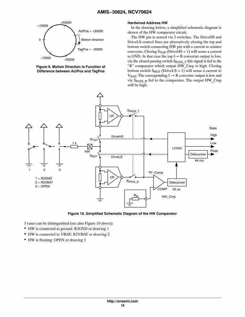
Hardwired Address HWIn the drawing below, a simplified schematic diagram is
shown of the HW comparator circuit.The HW pin is sensed via 2 switches. The DriveHS and
DriveLS control lines are alternatively closing the top andbottom switch connecting HW pin with a current to resistorconverter. Closing STOP (DriveHS = 1) will sense a currentto GND. In that case the top I� R converter output is low,via the closed passing switch SPASS_T this signal is fed to the“R” comparator which output HW_Cmp is high. Closingbottom switch SBOT (DriveLS = 1) will sense a current toVBAT. The corresponding I � R converter output is low andvia SPASS_B fed to the comparator. The output HW_Cmpwill be high.
1 2 3
1 = R2GND
COMP
I/R
LOGIC
High
Low
Float
DriveHS
DriveLS
HW_Cmp
HW
State
Debouncer
Debouncer
64 ms
1 k
Figure 10. Simplified Schematic Diagram of the HW Comparator
SBOT
STOP
I/R
Rth
32 �s
SPASS_B
‘‘R”−Comp
SPASS_T
2 = R2VBAT3 = OPEN
3 cases can be distinguished (see also Figure 10 above): HW is connected to ground: R2GND or drawing 1
HW is connected to VBAT: R2VBAT or drawing 2
HW is floating: OPEN or drawing 3
AMIS−30624, NCV70624
http://onsemi.com19
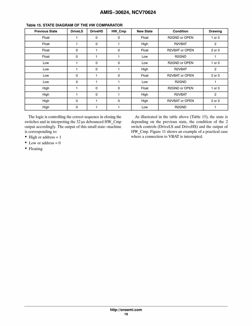
Table 15. STATE DIAGRAM OF THE HW COMPARATOR
Previous State DriveLS DriveHS HW_Cmp New State Condition Drawing
Float 1 0 0 Float R2GND or OPEN 1 or 3
Float 1 0 1 High R2VBAT 2
Float 0 1 0 Float R2VBAT or OPEN 2 or 3
Float 0 1 1 Low R2GND 1
Low 1 0 0 Low R2GND or OPEN 1 or 3
Low 1 0 1 High R2VBAT 2
Low 0 1 0 Float R2VBAT or OPEN 2 or 3
Low 0 1 1 Low R2GND 1
High 1 0 0 Float R2GND or OPEN 1 or 3
High 1 0 1 High R2VBAT 2
High 0 1 0 High R2VBAT or OPEN 2 or 3
High 0 1 1 Low R2GND 1
The logic is controlling the correct sequence in closing theswitches and in interpreting the 32 �s debounced HW_Cmpoutput accordingly. The output of this small state−machineis corresponding to: High or address = 1
Low or address = 0
Floating
As illustrated in the table above (Table 15), the state isdepending on the previous state, the condition of the 2switch controls (DriveLS and DriveHS) and the output ofHW_Cmp. Figure 11 shows an example of a practical casewhere a connection to VBAT is interrupted.
AMIS−30624, NCV70624
http://onsemi.com20
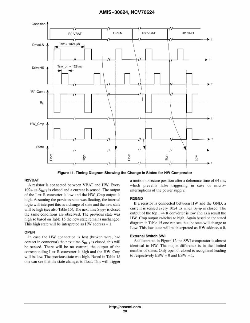
t
DriveLS
t
t
DriveHS
HW_Cmp
State
t
R2 VBAT OPEN
Hig
h
R2 VBAT R2 GND
t
Flo
at
Figure 11. Timing Diagram Showing the Change in States for HW Comparator
Flo
at
Hig
h
Rth
Condition
“R”−Comp
Tsw = 1024 �s
Tsw_on = 128 �s
t
Low
R2VBATA resistor is connected between VBAT and HW. Every
1024 �s SBOT is closed and a current is sensed. The outputof the I R converter is low and the HW_Cmp output ishigh. Assuming the previous state was floating, the internallogic will interpret this as a change of state and the new statewill be high (see also Table 15). The next time SBOT is closedthe same conditions are observed. The previous state washigh so based on Table 15 the new state remains unchanged.This high state will be interpreted as HW address = 1.
OPENIn case the HW connection is lost (broken wire, bad
contact in connector) the next time SBOT is closed, this willbe sensed. There will be no current, the output of thecorresponding I R converter is high and the HW_Cmpwill be low. The previous state was high. Based in Table 15one can see that the state changes to float. This will trigger
a motion to secure position after a debounce time of 64 ms,which prevents false triggering in case of micro−interruptions of the power supply.
R2GNDIf a resistor is connected between HW and the GND, a
current is sensed every 1024 �s when STOP is closed. Theoutput of the top I R converter is low and as a result theHW_Cmp output switches to high. Again based on the stateddiagram in Table 15 one can see that the state will change toLow. This low state will be interpreted as HW address = 0.
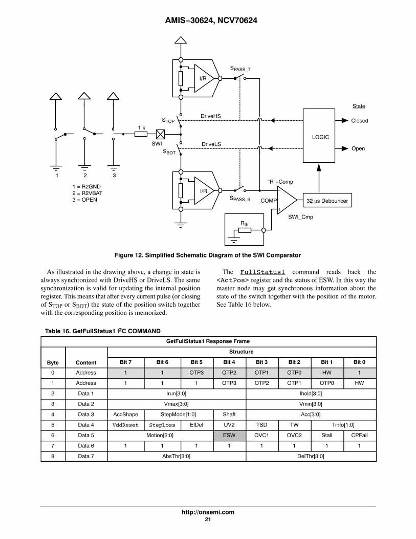
External Switch SWIAs illustrated in Figure 12 the SWI comparator is almost
identical to HW. The major difference is in the limitednumber of states. Only open or closed is recognized leadingto respectively ESW = 0 and ESW = 1.
AMIS−30624, NCV70624
http://onsemi.com21
COMP
I/R
LOGIC
Closed
Open
DriveHS
DriveLS
SWI_Cmp
SWI
1 2 3
1 = R2GND
1 k
Figure 12. Simplified Schematic Diagram of the SWI Comparator
2 = R2VBAT3 = OPEN
SBOT
STOP
32 �s Debouncer
Rth
I/R
State
SPASS_B
SPASS_T
‘‘R”−Comp
As illustrated in the drawing above, a change in state isalways synchronized with DriveHS or DriveLS. The samesynchronization is valid for updating the internal positionregister. This means that after every current pulse (or closingof STOP or SBOT) the state of the position switch togetherwith the corresponding position is memorized.
The FullStatus1 command reads back the<ActPos> register and the status of ESW. In this way themaster node may get synchronous information about thestate of the switch together with the position of the motor.See Table 16 below.
Table 16. GetFullStatus1 I2C COMMAND
GetFullStatus1 Response Frame
Byte Content
Structure
Bit 7 Bit 6 Bit 5 Bit 4 Bit 3 Bit 2 Bit 1 Bit 0
0 Address 1 1 OTP3 OTP2 OTP1 OTP0 HW 1
1 Address 1 1 1 OTP3 OTP2 OTP1 OTP0 HW
2 Data 1 Irun[3:0] Ihold[3:0]
3 Data 2 Vmax[3:0] Vmin[3:0]
4 Data 3 AccShape StepMode[1:0] Shaft Acc[3:0]
5 Data 4 VddReset StepLoss ElDef UV2 TSD TW Tinfo[1:0]
6 Data 5 Motion[2:0] ESW OVC1 OVC2 Stall CPFail
7 Data 6 1 1 1 1 1 1 1 1
8 Data 7 AbsThr[3:0] DelThr[3:0]

AMIS−30624, NCV70624
http://onsemi.com22
DriveHS
t
t
t
DriveLS
SWI_Cmp
ESW
t
t
0 1 1 1
ActPos
t
Figure 13. Simplified Timing Diagram Showing the Change in States for SWI Comparator
Act
Pos
Act
Pos
+ 1
Act
Pos
+ 2
Act
Pos
+ 3
Rth
“R”−Comp
512 �s
120 �s
Tsw = 1024 �s
Tsw_on = 128 �s
Main Control and Register, OTP memory + ROM
Power−up PhasePower−up phase of the AMIS−30624/NCV70624 will not
exceed 10 ms. After this phase, theAMIS−30624/NCV70624 is in standby mode, ready toreceive I2C messages and execute the associated commands.After power−up, the registers and flags are in the reset state,while some of them are being loaded with the OTP memorycontent (see Table 19: RAM Registers).
ResetAfter power−up, or after a reset occurrence (e.g. a
micro−cut on pin VBB has made VDD to go below VddReset
level), the H−bridges will be in high−impedance mode, andthe registers and flags will be in a predetermined position.This is documented in Table 19: RAM Registers andTable 20: Flags Table.
Soft−stopA soft−stop is an immediate interruption of a motion, but
with a deceleration phase. At the end of this action, theregister <TagPos> is loaded with the value contained inregister <ActPos>, see Table 19: Ram Registers). Thecircuit is then ready to execute a new positioning command,provided thermal and electrical conditions allow for it.

AMIS−30624, NCV70624
http://onsemi.com23
Thermal Shutdown ModeWhen thermal shutdown occurs, the circuit performs a
<SoftStop> command and goes to motor shutdownmode (see Figure 14: State Diagram TemperatureManagement).
Temperature ManagementThe AMIS−30624/NCV70624 monitors temperature by
means of two thresholds and one shutdown level, as
illustrated in the state diagram and illustration of Figure 14:State Diagram Temperature Management below. The onlycondition to reset flags <TW> and <TSD> (respectivelythermal warning and thermal shutdown) is to be at atemperature lower than Ttw and to get the occurrence of aGetFullStatus1 I2C frame.
Normal Temp.
− <Tinfo> = “00”− <TW> = ‘0’− <TSD> = ‘0’
T < Ttw &
GetFullStatus1
T > TtwThermal warning
− <Tinfo> = “10”− <TW> = ‘1’− <TSD> = ‘0’
T > TtsdThermal shutdown
− <Tinfo> = “11”− <TW> = ‘1’− <TSD> = ‘1’−SoftStop if motion ongoing− Motor shutdown (motion disabled)
Post thermalwarning
− <Tinfo> = “00”− <TW> = ‘1’− <TSD> = ‘0’
T > Tlow
T > Ttw
T < TtsdT > Ttsd
Post thermalshutdown 1
− <Tinfo> = “10”− <TW> = ‘1’− <TSD> = ‘1’− Motor shutdown (motion disabled)
Post thermalshutdown 2
− <Tinfo> = “00”− <TW> = ‘1’− <TSD> = ‘1’− Motor shutdown (motion disabled)
Low Temp.
− <Tinfo> = “01”− <TW> = ‘0’− <TSD> = ‘0’
T < Ttw
T > Ttw
T < Tlow
T < Ttw
Figure 14. State Diagram Temperature Management
I2C Frame:

AMIS−30624, NCV70624
http://onsemi.com24
T warning level
T shutdown level
T
t
getfullstatus1
T > Ttsd, motorstops andshutdown getfullstatus1
Figure 15. Illustration of Thermal Management Situation
T <tw> bit
T <tsd> bitT < Ttw and
T < Ttw and
Autarkic Functionality in Under−VoltageCondition
Battery Voltage ManagementThe AMIS−30624/NCV70624 monitors the battery
voltage by means of one threshold and one shutdown level.The only condition to reset flags <UV2> and <StepLoss>is to recover by a battery voltage higher than UV1 and toreceive a GetFullStatus1 command.
Autarkic FunctionThe device enters states <HardUnder> (see Figure 16),
followed by <ShutUnder> when VBB is below the UV2level or <CPFail> = 1. The motion is stopped immediatelyand Target Position (TagPos) is kept and not overwritten byActual Position (ActPos). The motor is in HiZ state and theflags <UV2> and <Steploss> are set to inform the masterthat the voltage has dropped below UV2 or the charge pumpvoltage has dropped below the level of the charge pumpcomparator and loss of steps is possible. If in this state VBB becomes > UV1 within 15 seconds,
then AMIS−30624/NCV70624 returns to <Stopped>state. From there, it resumes the interrupted motion andaccepts updates of the target position by means of thecommands SetPosition and
GotoSecurePosition, even if the <UV2> flag, the<CPFail> flag and <Steploss> flags are NOTcleared.
If however the VBB voltage remains below UV2 levelor the charge pump voltage level is below the chargepump comparator for more than 15 seconds, then thedevice will enter <Shutdown> state and the targetposition is overwritten by Actual Position. This statecan be exited only if VBB is > UV1, the charge pumpvoltage is above the charge pump comparator voltageand an incoming command GetFullStatus1 isreceived.
Important Notes:1. In the case of Autarkic positioning, care needs to
be taken because accumulated steploss can cause asignificant deviation between physical and storedactual position.
2. The SetDualPosition command will only beexecuted after clearing the <UV2>, CPFail and<Steploss> flags.
3. RAM reset occurs when Vdd < VddReset (digitalPower−On−Reset level).
4. The Autarkic function remains active as long asVDD > VddReset.

AMIS−30624, NCV70624
http://onsemi.com25
OTP Register
OTP Memory StructureThe table below shows how the parameters to be stored in the OTP memory are located.
Table 17. OTP MEMORY STRUCTURE
Address Bit 7 Bit 6 Bit 5 Bit 4 Bit 3 Bit 2 Bit 1 Bit 0
0x00 OSC3 OSC2 OSC1 OSC0 IREF3 IREF2 IREF1 IREF0
0x01 0 TSD2 TSD1 TSD0 BG3 BG2 BG1 BG0
0x02 AbsThr3 AbsThr2 AbsThr1 AbsThr0 PA3 PA2 PA1 PA0
0x03 Irun3 Irun2 Irun1 Irun0 Ihold3 Ihold2 Ihold1 Ihold0
0x04 Vmax3 Vmax2 Vmax1 Vmax0 Vmin3 Vmin2 Vmin1 Vmin0
0x05 SecPos10 SecPos9 SecPos8 Shaft Acc3 Acc2 Acc1 Acc0
0x06 SecPos7 SecPos6 SecPos5 SecPos4 SecPos3 SecPos2
0x07 DelThr3 DelThr2 DelThr1 DelThr0 StepMode1 StepMode0 LOCKBT LOCKBG
Parameters stored at address 0x00 and 0x01 and bit<LOCKBT> are already programmed in the OTP memory atcircuit delivery. They correspond to the calibration of thecircuit and are just documented here as an indication.
Each OTP bit is at ‘0’ when not zapped. Zapping a bit willset it to ‘1’. Thus only bits having to be at ‘1’ must be zapped.Zapping of a bit already at ‘1’ is disabled. Each OTP bytewill be programmed separately (see commandSetOTPparam). Once OTP programming is completed, bit<LOCKBG> can be zapped to disable future zapping,otherwise any OTP bit at ‘0’ could still be zapped by usinga SetOTPparam command.
Table 18. OTP OVERWRITE PROTECTION
Lock Bit Protected Bytes
LOCKBT (factory zappedbefore delivery)
0x00 to 0x01
LOCKBG 0x00 to 0x07
The command used to load the application parameters viathe I2C bus in the RAM prior to an OTP Memoryprogramming is SetMotorParam. This allows for afunctional verification before using a SetOTPparamcommand to program and zap separately one OTP memorybyte. A GetOTPparam command issued after eachSetOTPparam command allows verifying the correct bytezapping.
Note: Zapped bits will become active only after a powercycle. After programming the I2C bits the power cycle hasto be performed first to guarantee further communicationwith the device.
Application Parameters Stored in OTP MemoryExcept for the physical address <PA[3:0]> these
parameters, although programmed in a non−volatilememory can still be overridden in RAM by a I2C writingoperation.
PA[3:0] In combination with hired wired (HW)address, it forms the physical address AD[6:0]of the stepper−motor. Up to 32 stepper motorscan theoretically be connected to the same I2Cbus.
AbsThr[3:0] Absolute threshold used for themotion detection
Index AbsThr AbsThr level (V) (*)
0 0 0 0 0 Disable
1 0 0 0 1 0.5
2 0 0 1 0 1.0
3 0 0 1 1 1.5
4 0 1 0 0 2.0
5 0 1 0 1 2.5
6 0 1 1 0 3.0
7 0 1 1 1 3.5
8 1 0 0 0 4.0
9 1 0 0 1 4.5
A 1 0 1 0 5.0
B 1 0 1 1 5.5
C 1 1 0 0 6.0
D 1 1 0 1 6.5
E 1 1 1 0 7.0
F 1 1 1 1 7.5
(*) Not tested in production. Values are approximations.

AMIS−30624, NCV70624
http://onsemi.com26
DelThr[3:0] Relative threshold used for themotion detection
Index DelThr DelThr Level (V) (*)
0 0 0 0 0 Disable
1 0 0 0 1 0.25
2 0 0 1 0 0.50
3 0 0 1 1 0.75
4 0 1 0 0 1.00
5 0 1 0 1 1.25
6 0 1 1 0 1.50
7 0 1 1 1 1.75
8 1 0 0 0 2.00
9 1 0 0 1 2.25
A 1 0 1 0 2.50
B 1 0 1 1 2.75
C 1 1 0 0 3.00
D 1 1 0 1 3.25
E 1 1 1 0 3.50
F 1 1 1 1 3.75
(*) Not tested in production. Values are approximations.
Irun[3:0] Current amplitude value to be fed toeach coil of the stepper−motor. The table belowprovides the 16 possible values for <IRUN>.
Index Irun Run Current (mA)
0 0 0 0 0 59
1 0 0 0 1 71
2 0 0 1 0 84
3 0 0 1 1 100
4 0 1 0 0 119
5 0 1 0 1 141
6 0 1 1 0 168
7 0 1 1 1 200
8 1 0 0 0 238
9 1 0 0 1 283
A 1 0 1 0 336
B 1 0 1 1 400
C 1 1 0 0 476
D 1 1 0 1 566
E 1 1 1 0 673
F 1 1 1 1 800
Ihold[3:0] Hold current for each coil of thestepper−motor. The table below provides the 16possible values for <IHOLD>.
Index Ihold Hold Current (mA)
0 0 0 0 0 59
1 0 0 0 1 71
2 0 0 1 0 84
3 0 0 1 1 100
4 0 1 0 0 119
5 0 1 0 1 141
6 0 1 1 0 168
7 0 1 1 1 200
8 1 0 0 0 238
9 1 0 0 1 283
A 1 0 1 0 336
B 1 0 1 1 400
C 1 1 0 0 476
D 1 1 0 1 566
E 1 1 1 0 673
F 1 1 1 1 0
Note: When the motor is stopped, the current is reducedfrom <IRUN> to <IHOLD>. In the case of 0 mA holdcurrent (1111 in the hold current table), the followingsequence is applied:
1. The current is first reduced to 59 mA(corresponding to 0000 value in the table).
2. The PWM regulator is switched off; the bottomtransistors of the bridges are grounded.
StepMode Setting of step modes.
StepMode Step Mode
0 0 1/2 stepping
0 1 1/4 stepping
1 0 1/8 stepping
1 1 1/16 stepping
Shaft This bit distinguishes between a clock−wiseor counter−clock−wise rotation. The shaft bit isnot working in RunVelocity mode.
SecPos[10:2] Secure Position of thestepper−motor. This is the position to which themotor is driven in case of a HW pin connectionis lost. If <SecPos[10:2]> = “100 000000xx”, secure positioning is disabled; thestepper−motor will be kept in the positionoccupied at the moment these events occur.
AMIS−30624, NCV70624
http://onsemi.com27
Note: The Secure Position is coded on 11 bits only,providing actually the most significant bits of the position, thenon coded least significant bits being set to ‘0’. The SecurePosition in OTP has only 9 bits. The two least significant bitsare loaded as ‘0’ to RAM when copied from OTP.
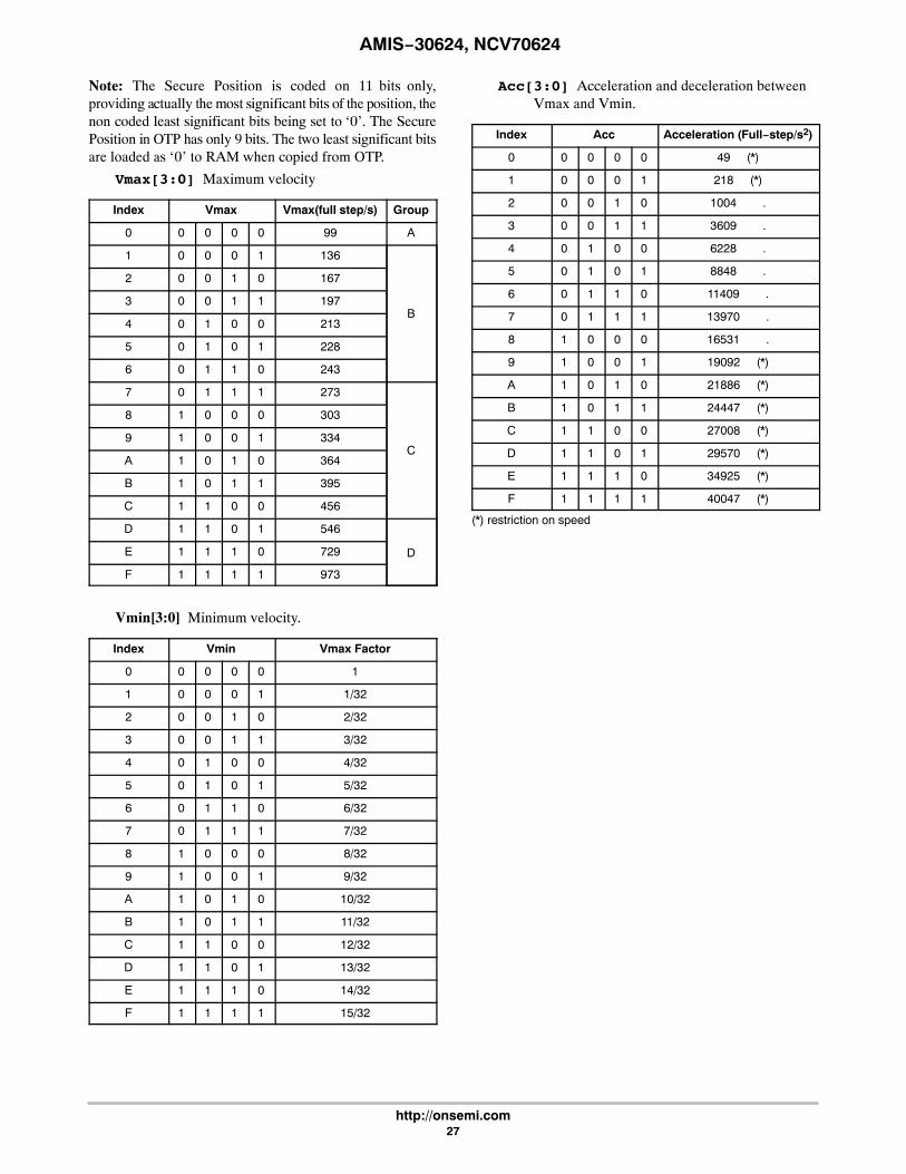
Vmax[3:0] Maximum velocity
Index Vmax Vmax(full step/s) Group
0 0 0 0 0 99 A
1 0 0 0 1 136
B
2 0 0 1 0 167
3 0 0 1 1 197
4 0 1 0 0 213
5 0 1 0 1 228
6 0 1 1 0 243
7 0 1 1 1 273
C
8 1 0 0 0 303
9 1 0 0 1 334
A 1 0 1 0 364
B 1 0 1 1 395
C 1 1 0 0 456
D 1 1 0 1 546
DE 1 1 1 0 729
F 1 1 1 1 973
Vmin[3:0] Minimum velocity.
Index Vmin Vmax Factor
0 0 0 0 0 1
1 0 0 0 1 1/32
2 0 0 1 0 2/32
3 0 0 1 1 3/32
4 0 1 0 0 4/32
5 0 1 0 1 5/32
6 0 1 1 0 6/32
7 0 1 1 1 7/32
8 1 0 0 0 8/32
9 1 0 0 1 9/32
A 1 0 1 0 10/32
B 1 0 1 1 11/32
C 1 1 0 0 12/32
D 1 1 0 1 13/32
E 1 1 1 0 14/32
F 1 1 1 1 15/32
Acc[3:0] Acceleration and deceleration betweenVmax and Vmin.
Index Acc Acceleration (Full−step/s2)
0 0 0 0 0 49 (*)
1 0 0 0 1 218 (*)
2 0 0 1 0 1004 .
3 0 0 1 1 3609 .
4 0 1 0 0 6228 .
5 0 1 0 1 8848 .
6 0 1 1 0 11409 .
7 0 1 1 1 13970 .
8 1 0 0 0 16531 .
9 1 0 0 1 19092 (*)
A 1 0 1 0 21886 (*)
B 1 0 1 1 24447 (*)
C 1 1 0 0 27008 (*)
D 1 1 0 1 29570 (*)
E 1 1 1 0 34925 (*)
F 1 1 1 1 40047 (*)
(*) restriction on speed
AMIS−30624, NCV70624
http://onsemi.com28
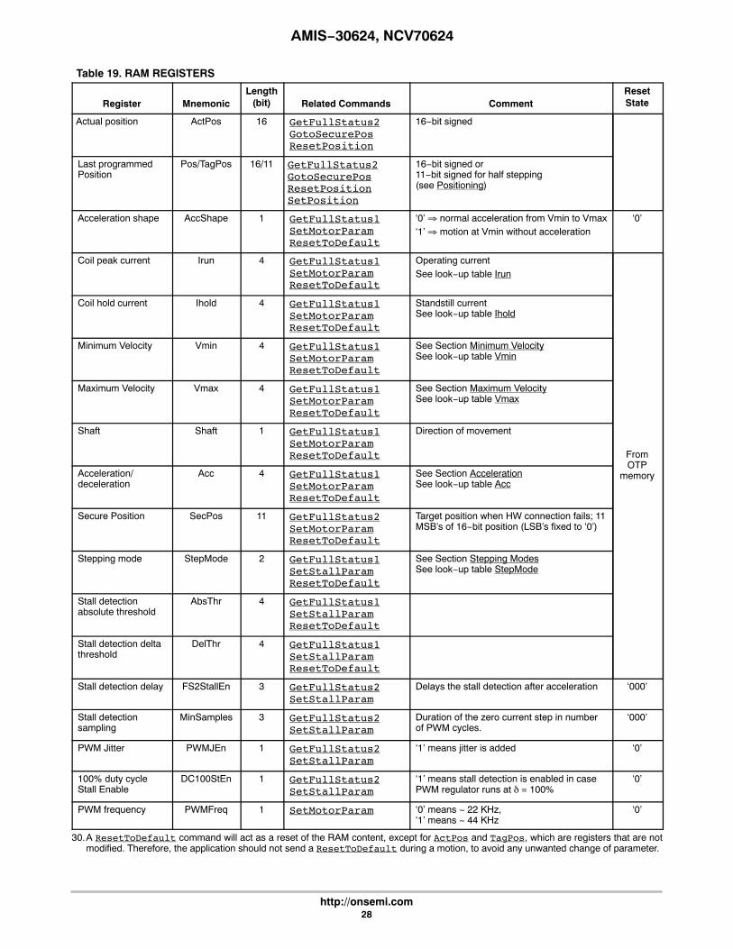
Table 19. RAM REGISTERS
Register MnemonicLength
(bit) Related Commands CommentResetState
Actual position ActPos 16 GetFullStatus2GotoSecurePosResetPosition
16−bit signed
Last programmedPosition
Pos/TagPos 16/11 GetFullStatus2GotoSecurePosResetPositionSetPosition
16−bit signed or11−bit signed for half stepping(see Positioning)
Acceleration shape AccShape 1 GetFullStatus1SetMotorParamResetToDefault
‘0’ normal acceleration from Vmin to Vmax‘1’ motion at Vmin without acceleration
‘0’
Coil peak current Irun 4 GetFullStatus1SetMotorParamResetToDefault
Operating currentSee look−up table Irun
FromOTP
memory
Coil hold current Ihold 4 GetFullStatus1SetMotorParamResetToDefault
Standstill currentSee look−up table Ihold
Minimum Velocity Vmin 4 GetFullStatus1SetMotorParamResetToDefault
See Section Minimum VelocitySee look−up table Vmin
Maximum Velocity Vmax 4 GetFullStatus1SetMotorParamResetToDefault
See Section Maximum VelocitySee look−up table Vmax
Shaft Shaft 1 GetFullStatus1SetMotorParamResetToDefault
Direction of movement
Acceleration/deceleration
Acc 4 GetFullStatus1SetMotorParamResetToDefault
See Section AccelerationSee look−up table Acc
Secure Position SecPos 11 GetFullStatus2SetMotorParamResetToDefault
Target position when HW connection fails; 11MSB’s of 16−bit position (LSB’s fixed to ‘0’)
Stepping mode StepMode 2 GetFullStatus1SetStallParamResetToDefault
See Section Stepping ModesSee look−up table StepMode
Stall detectionabsolute threshold
AbsThr 4 GetFullStatus1SetStallParamResetToDefault
Stall detection deltathreshold
DelThr 4 GetFullStatus1SetStallParamResetToDefault
Stall detection delay FS2StallEn 3 GetFullStatus2SetStallParam
Delays the stall detection after acceleration ‘000’
Stall detectionsampling
MinSamples 3 GetFullStatus2SetStallParam
Duration of the zero current step in numberof PWM cycles.
‘000’
PWM Jitter PWMJEn 1 GetFullStatus2SetStallParam
‘1’ means jitter is added ‘0’
100% duty cycleStall Enable
DC100StEn 1 GetFullStatus2SetStallParam
‘1’ means stall detection is enabled in casePWM regulator runs at � = 100%
‘0’
PWM frequency PWMFreq 1 SetMotorParam ‘0’ means ~ 22 KHz,‘1’ means ~ 44 KHz
‘0’
30.A ResetToDefault command will act as a reset of the RAM content, except for ActPos and TagPos, which are registers that are notmodified. Therefore, the application should not send a ResetToDefault during a motion, to avoid any unwanted change of parameter.

AMIS−30624, NCV70624
http://onsemi.com29
Table 20. FLAGS TABLE
Flag MnemonicLength
(bit) Related Commands CommentResetState
Charge pump failure CPFail 1 GetFullStatus1 ‘0’ = charge pump OK‘1’ = charge pump failureResets only after GetFullStatus1
‘0’
Electrical defect ElDef 1 GetFullStatus1 <OVC1> or <OVC2> or‘open−load on coil X’ or ‘open−load oncoil XY or <CPFail> Resets only after GetFullStatus1
‘0’
External switchstatus
ESW 1 GetFullStatus1 ‘0’ = open‘1’ = close
‘0’
Electrical flag HS 1 Internal use <CPFail> or <UV2> or <ElDef> or <VDDreset> ‘0’
Motion status Motion 3 GetFullStatus1 “x00” = Stop“001” = inner (CCW) motion acceleration“010” = inner (CCW) motion deceleration“011” = inner (CCW) motion max. speed“101” = outer (CW) motion acceleration“110” = outer (CW) motion deceleration“111” = outer (CW) motion max. speed
“000”
Over current in coil X OVC1 1 GetFullStatus1 ‘1’ = over current; reset only after GetFull-Status1 ‘0’
Over current in coil Y OVC2 1 GetFullStatus1 ‘1’ = over current; reset only after GetFull-Status1 ‘0’
Secure positionenabled
SecEn 1 Internal use ‘0’ if <SecPos> = “100 0000 0000”‘1’ otherwise n.a.
Step loss StepLoss 1 GetFullStatus1 ‘1’ = step loss due to under voltage, over current,open circuit or stall; Resets only after GetFull-Status1
‘1’
Delta High Stall DelStallHi 1 GetFullStatus2 ‘1’ = Vbemf > Ubemf + DeltaThr ‘0’
Delta Low Stall DelStallLo 1 GetFullStatus2 ‘1’ = Vbemf < Ubemf − DeltaThr ‘0’
Absolute Stall AbsStall 1 GetFullStatus2 ‘1’ = Vbemf < AbsThr ‘0’
Stall Stall 1 GetFullStatus1 ‘0’
Motor stop Stop 1 Internal use ‘0’
Temperature info Tinfo 2 GetFullStatus1 “00” = normal temperature range“01” = low temperature warning“10” = high temperature warning“11” = motor shutdown
“00”
Thermal shutdown TSD 1 GetFullStatus1 ‘1’ = shutdown (Tj > Ttsd)Resets only after GetFullStatus1and if <Tinfo> = “00”
‘0’
Thermal warning TW 1 GetFullStatus1 ‘1’ = over temperature (Tj > Ttw)Resets only after GetFullStatus1and if <Tinfo> = “00”
‘0’
Battery stop voltage UV2 1 GetFullStatus1 ‘0’ = VBB > UV2‘1’ = VBB UV2Resets only after GetFullStatus1
‘0’
Digital supply reset VddReset 1 GetActualPosGetStatusGetFullStatus1
Set at ‘1’ after power−up of the circuit. If this was due toa supply micro−cut, it warns that the RAM contentsmay have been lost; can be reset to ‘0’ with aGet(Full)Status1 command
‘1’

AMIS−30624, NCV70624
http://onsemi.com30
Priority EncoderThe table below describes the simplified state management performed by the main control block.
Table 21. PRIORITY ENCODERState � Standby Stopped GotoPos DualPosition SoftStop HardStop ShutDown HardUnder ShutUnder
Command�
MotorStopped,
Ihold in CoilsMotor Motion
Ongoing
No Influence onRAM and Tag-
PosMotor
DeceleratingMotor Forced to
Stop
Motor Stopped,H−bridges in
Hi−Z
GetOTPparam OTP refresh;I2C slaveresponse
OTP refresh;I2C slaveresponse
OTP refresh;I2C slaveresponse
OTP refresh;I2C slaveresponse
OTP refresh;I2C slaveresponse
OTP refresh;I2C slaveresponse
GetFullStatus1[attempt to clear
all flags]
(Note 31)
I2C slaveresponse
I2C slaveresponse
I2C slaveresponse
I2C slaveresponse
I2C slaveresponse
I2C slaveresponse;
if (<TSD> or<ElFlag> = ‘0’then Stopped
GetFullStatus2 I2C slaveresponse
I2C slaveresponse
I2C slaveresponse
I2C slaveresponse
I2C slaveresponse
I2C slaveresponse
ResetToDefault[ ActPos andTagPos are not
altered ]
OTP refresh;OTP to RAM;AccShape
reset
OTP refresh;OTP to RAM;
AccShape reset
OTP refresh;OTP to RAM;
AccShape reset(Note 33)
OTP refresh;OTP to RAM;
AccShape reset
OTP refresh;OTP to RAM;
AccShape reset
OTP refresh;OTP to RAM;
AccShape reset
SetMotorParam[Master takes
care aboutproper update]
RAM update RAM update RAM update RAM update RAM update RAM update RAM update RAM update RAM update
ResetPosition <TagPos> and<ActPos> reset
<TagPos> and<ActPos>
reset
<TagPos> and<ActPos>
reset
SetPosition <TagPos>updated;
GotoPos
<TagPos> updated
<TagPos> updated
SetPositionShort <TagPos> updated;
GotoPos
<TagPos> updated
<TagPos> updated
GotoSecPosition If <SecEn> =‘1’ then
<TagPos> =<SecPos>; GotoPos
If <SecEn> = ‘1’then <TagPos> =
<SecPos>
If <SecEn> = ‘1’then <TagPos> =
<SecPos>
DualPosition DualPosition
SoftStop SoftStop
HardStop HardStop HardStop HardStop
VBB < UV2 andt > 15 seconds
HardUnder HardUnder HardStop HardUnder
VBB < UV2 andt < 15 seconds
Stopped
<ElDef> = ‘1’ <HS> = ‘1’
Shutdown HardStop;<StepLoss> = ‘1’
HardStop;<StepLoss> = ‘1’
HardStop;<StepLoss> = ‘1’
Shutdown
Thermalshutdown
[<TSD> = ‘1’]
Shutdown SoftStop SoftStop Shutdown
Motion finished n.a. Stopped Stopped Stopped;<TagPos> =<ActPos>
Stopped;<TagPos> =<ActPos>
n.a.
With the Following Color Code:
Command Ignored Transition to Another State Master is responsible for proper update (see Note 36)
NOTE: See table notes on the following page.

AMIS−30624, NCV70624
http://onsemi.com31
31.<ElFlag> = <CPFail> or <UV2> or <ElDef> or <VDDreset>32.After power−on−reset, the <Standby> state is entered.33.A DualPosition sequence runs with a separate set of RAM registers. The parameters that are not specified in a DualPosition command are
loaded with the values stored in RAM at the moment the DualPosition sequence starts. <AccShape> is forced to ‘1’ during second motion.<AccShape> at ‘0’ will be taken into account after the DualPosition sequence. A GetFullStatus1 command will return the defaultparameters for <Vmax> and <Vmin> stored in RAM.
34.Shutdown state can be left only when <TSD> and <HS> flags are reset.35.Flags can be reset only after the master could read them via a GetFullStatus1 command, and provided the physical conditions allow
for it (normal temperature, correct battery voltage and no electrical or charge pump defect).36.A SetMotorParam command sent while a motion is ongoing (state <GotoPos>) should not attempt to modify <Acc> and <Vmin> values.
This can be done during a DualPosition sequence since this motion uses its own parameters, the new parameters will be taken into accountat the next SetPosition command.
37.<SecEn> = ‘1’ when register <SecPos> is loaded with a value different from the most negative value (i.e. different from 0x400 = “100 00000000”).
38.<Stop> flag allows distinguishing whether state <Stopped> was entered after HardStop/SoftStop or not. <Stop> is set to ‘1’ when leavingstate <HardStop> or <SoftStop> and is reset during first clock edge occurring in state <Stopped>.
39.While in state <Stopped>, if <ActPos> <TagPos> there is a transition to state <GotoPos>. This transition has the lowest priority,meaning that <Stop>, <TSD>, etceteras are first evaluated for possible transitions.
40. If <StepLoss> is active, then SetPosition and GotoSecurePosition commands are not ignored. <StepLoss> can only be clearedby a GetFullStatus1 command.
HardStop
Stopped GotoPosShutdown
Thermal Shutdown
HardStop HardStop
HardStop
Dual Positioning Motion finished
GotoSecPos
SetPosition
Motion Finished
Motion Finished
ThermalShutDown
SoftStop
HardStopThermal Shutdown
Referencing Soft−stop
Priorities 1
2
3
4
Motion Finished
POR
HardUnder
ShutUnder
Vbb < UV2 or CPFAIL
Vbb < UV2 or CPFAIL
Vbb > UV1 and not CPFAIL
T > 15 sec
Figure 16. Simplified State Diagram
GetFullStatus1

AMIS−30624, NCV70624
http://onsemi.com32
Motordriver
Current Waveforms in the CoilsFigure 17 below illustrates the current fed to the motor coils by the motordriver in half−step mode.
t
Coil X
Coil Y
Ix
Iy
Figure 17. Current Waveforms in Motor Coils X and Y in Halfstep Mode
Whereas Figure 18 below shows the current fed to the coils in 1/16th micro stepping (1 electrical period).
t
Coil X
Coil Y
Ix
Iy
Figure 18. Current Waveforms in Motor Coils X and Y in 1/16th Micro−Step Mode
PWM RegulationIn order to force a given current (determined by <Irun>
or <Ihold> and the current position of the rotor) throughthe motor coil while ensuring high energy transferefficiency, a regulation based on PWM principle is used. Theregulation loop performs a comparison of the sensed outputcurrent to an internal reference, and features a digitalregulation generating the PWM signal that drives the outputswitches. The zoom over one micro−step in the Figure 18above shows how the PWM circuit performs this regulation.To reduce the current ripple, a higher PWM frequency isselectable. The RAM register PWMfreq is used for this.
Table 22. PWM FREQUENCY SELECTION
PWMfreq Applied PWM Frequency
0 22,8 kHz
1 45,6 kHz
PWM JitterTo lower the power spectrum for the fundamental and
higher harmonics of the PWM frequency, jitter can be addedto the PWM clock. The RAM register <PWMJEn> is usedfor this.
Table 23. PWM JITTER SELECTION
PWMJEn Status
0 Single PWM frequency
1 Added jitter to PWM frequency
AMIS−30624, NCV70624
http://onsemi.com33
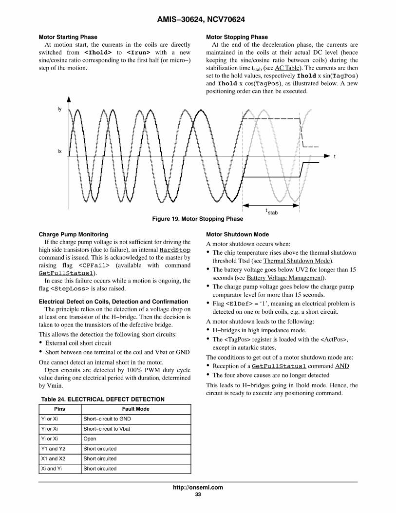
Motor Starting PhaseAt motion start, the currents in the coils are directly
switched from <Ihold> to <Irun> with a newsine/cosine ratio corresponding to the first half (or micro−)step of the motion.
Motor Stopping PhaseAt the end of the deceleration phase, the currents are
maintained in the coils at their actual DC level (hencekeeping the sine/cosine ratio between coils) during thestabilization time tstab (see AC Table). The currents are thenset to the hold values, respectively Ihold x sin(TagPos)and Ihold x cos(TagPos), as illustrated below. A newpositioning order can then be executed.
tIx
Iy
t stabFigure 19. Motor Stopping Phase
Charge Pump MonitoringIf the charge pump voltage is not sufficient for driving the
high side transistors (due to failure), an internal HardStopcommand is issued. This is acknowledged to the master byraising flag <CPFail> (available with commandGetFullStatus1).
In case this failure occurs while a motion is ongoing, theflag <StepLoss> is also raised.
Electrical Defect on Coils, Detection and ConfirmationThe principle relies on the detection of a voltage drop on
at least one transistor of the H−bridge. Then the decision istaken to open the transistors of the defective bridge.
This allows the detection the following short circuits: External coil short circuit
Short between one terminal of the coil and Vbat or GND
One cannot detect an internal short in the motor.Open circuits are detected by 100% PWM duty cycle
value during one electrical period with duration, determinedby Vmin.
Table 24. ELECTRICAL DEFECT DETECTION
Pins Fault Mode
Yi or Xi Short−circuit to GND
Yi or Xi Short−circuit to Vbat
Yi or Xi Open
Y1 and Y2 Short circuited
X1 and X2 Short circuited
Xi and Yi Short circuited
Motor Shutdown Mode
A motor shutdown occurs when: The chip temperature rises above the thermal shutdown
threshold Ttsd (see Thermal Shutdown Mode). The battery voltage goes below UV2 for longer than 15
seconds (see Battery Voltage Management). The charge pump voltage goes below the charge pump
comparator level for more than 15 seconds. Flag <ElDef> = ‘1’, meaning an electrical problem is
detected on one or both coils, e.g. a short circuit.
A motor shutdown leads to the following: H−bridges in high impedance mode.
The <TagPos> register is loaded with the <ActPos>,except in autarkic states.
The conditions to get out of a motor shutdown mode are: Reception of a GetFullStatus1 command AND
The four above causes are no longer detected
This leads to H−bridges going in Ihold mode. Hence, thecircuit is ready to execute any positioning command.

AMIS−30624, NCV70624
http://onsemi.com34
This can be illustrated in the following sequence given as an application example. The master can check whether there isa problem or not and decide which application strategy to adopt.
Table 25. Example of Possible Sequence used to Detect and Determine Cause of Motor Shutdown
Tj Tsd orVBB UV2 (>15s) or
<ElDef> = ‘1’ or<CPFail> = ‘1’ (>15s)
SetPositionframe
GetFullStatus1 frame
GetFullStatus1 frame
...
− The circuit is driven in motor shutdownmode
− The application is not aware of this
− The position set−point isupdated by the I2C Master− Motor shutdown mode
no motion− The application is still
unaware
− The application is awareof a problem
− Possible confirmation ofthe problem
− Reset <TW> or <TSD> or <UV2> or <StepLoss> or<ElDef> or <CPFail> by the application
− Possible new detection of over temperature or lowvoltage or electrical problem Circuit sets <TW> or
<TSD> or <UV2> or <StepLoss> or <ElDef> or<CPFail> again at ‘1’
Important: While in shutdown mode, since there is no holdcurrent in the coils, the mechanical load can cause a step loss,which indeed cannot be flagged by theAMIS−30624/NCV70624.
Note: The Priority Encoder is describing the management ofstates and commands.
Warning: The application should limit the number ofconsecutive GetFullStatus1 commands to try to get theAMIS−30624/NCV70624 out of shutdown mode when thisproves to be unsuccessful, e.g. there is a permanent defect.The reliability of the circuit could be altered sinceGetFullStatus1 attempts to disable the protection of theH−bridges.
Motion DetectionMotion detection is based on the back emf generated
internally in the running motor. When the motor is blocked,e.g. when it hits the end−stop, the velocity and as a result alsothe generated back emf, is disturbed. TheAMIS−30624/NCV70624 senses the back emf, calculates a
moving average and compares the value with twoindependent threshold levels: Absolute threshold(AbsThr[3:0]) and Delta threshold (<DelThr[3:0]>).Instructions for correct use of these two levels incombination with three additional parameters(<MinSamples>, <FS2StallEn> and <DC100StEn>)are available in a dedicated Application Note “RobustMotion Control with AMIS−3062x Stepper Motor Drivers”.
If the motor is accelerated by a pulling or propelling forceand the resulting back emf increases above the Deltathreshold (+�THR), then <DelStallHi> is set. When themotor is slowing down and the resulting back emf decreasesbelow the Delta threshold (−�THR), then <DelStallLo>is set. When the motor is blocked and the velocity is zeroafter the acceleration phase, the back emf is low or zero.When this value is below the Absolute threshold,<AbsStall> is set. The <Stall> flag is the OR functionof <DelStallLo> OR <DelStallHi> OR<AbsStall>.
AbsStall
t
Velocity
t
Motor speed
Vbemf
VABSTH
t
Back emf
Vbemf
DeltaStallHi
t
t
DeltaStallLo
t
Figure 20. Triggering of the Stall Flags in Function of Measured Backemf and the Set Threshold Levels
VbemfVbemf
Vmin
Vmax+�THR
−�THR

AMIS−30624, NCV70624
http://onsemi.com35
Table 26. TRUTH TABLE
Condition <DelStallLo> <DelStallHi> <AbsStall> <Stall>
Vbemf < Average − DelThr 1 0 0 1
Vbemf > Average + DelThr 0 1 0 1
Vbemf < AbsThr 0 0 1 1
By design, the motion will only be detected when themotor is running at the maximum velocity, not duringacceleration or deceleration.
If the motor is positioning when Stall is detected, an(internal) hardstop of the motor is generated and the<StepLoss> and <Stall> flags are set. These flags canonly be reset by sending a GetFullStatus1 command.
If Stall appears during DualPosition then the first phase iscancelled (via internal hardstop) and after timeout Tstab (seeAC table) the second phase at Vmin starts.
When the <Stall> flag is set the position controller willgenerate an internal HardStop. As a consequence also the<Steploss> flag will be set. The position in the internalcounter will be copied to the <ActPos> register. All flagscan be read out with the GetFullStatus1 command.
Important Remark (limited to motion detection flags /parameters):
Using GetFullStatus1 will read AND clear thefollowing flags: <Steploss>, <Stall>, <AbsStall>,<DelStallLo> and <DelStallHi>. New positioning ispossible and the <ActPos> register will be further updated.
Motion detection is disabled when the RAM registers<AbsThr[3:0]> and <DelThr[3:0]> are zero. Bothlevels can be programmed using the I2C commandSetStallParam in the registers <AbsThr[3:0]> and<DelThr[3:0]>. Also the OTP register<AbsThr[3:0]> and <DelThr[3:0]> can be setusing the I2C command SetOTPParam. These values arecopied in the RAM registers during power on reset.
Table 27. ABSOLUTE AND DELTA THRESHOLD SETTINGS
AbsThrIndex
AbsThrLevel (V) (*)
DelThrIndex
DelThrLevel (V) (*)
0 Disable 0 Disable
1 0.5 1 0.25
2 1.0 2 0.50
3 1.5 3 0.75
4 2.0 4 1.00
5 2.5 5 1.25
6 3.0 6 1.50
7 3.5 7 1.75
8 4.0 8 2.00
9 4.5 9 2.25
A 5.0 A 2.50
B 5.5 B 2.75
C 6.0 C 3.00
D 6.5 D 3.25
E 7.0 E 3.50
F 7.5 F 3.75
(*) Not tested in production. Values are approximations.
MinSamples<MinSamples[2:0]> is a programmable delay timer.
After the zero crossing is detected, the delay counter isstarted. After the delay time−out (tdelay) the back−emfsample is taken. For more information please refer to theApplication Note “Robust Motion Control withAMIS−3062x Stepper Motor Drivers”.
Table 28. BACK EMF SAMPLE DELAY TIME
Index MinSamples[2:0] tDELAY (�s)
0 000 87
1 001 130
2 010 174
3 011 217
4 100 261
5 101 304
6 110 348
7 111 391

AMIS−30624, NCV70624
http://onsemi.com36
FS2StallEnIf <AbsThr> or <DelThr> <> 0 (i.e. motion detection
is enabled), then stall detection will be activated AFTER theacceleration ramp + an additional number of full−steps,according to the following table:
Table 29. ACTIVATION DELAY OF MOTIONDETECTION
Index FS2StallEn[2:0] Delay (Full Steps)
0 000 0
1 001 1
2 010 2
3 011 3
4 100 4
5 101 5
6 110 6
7 111 7
DC100StEnWhen a motor with large bemf is operated at high speed
and low supply voltage, then the PWM duty cycle can be as
high as 100%. This indicates that the supply is too low togenerate the required torque and might also result inerroneously triggering the stall detection. The bit<DC100StEn> enables stall detection when duty cycle is100%. For more information please refer to the ApplicationNote “Robust Motion Control with AMIS−3062x StepperMotor Drivers”.
Motion Qualification Mode (*)This mode is useful to debug motion parameters and to
verify the stability of stepper motor systems. The motionqualification mode is entered by means of the I2C commandTestBemf. The SWI pin will be converted into ananalogue output on which the Back EMF integrator outputcan be measured. Once activated, it can only be stopped aftera POR. During the Back emf observation, reading of theSWI state is internally forbidden.
(*) Note: Not applicable for product versionsNCV70624DW010G, NCV70624DW010R2G.
More information is available in the Application Note“Robust Motion Control with AMIS−3062x Stepper MotorDrivers”.
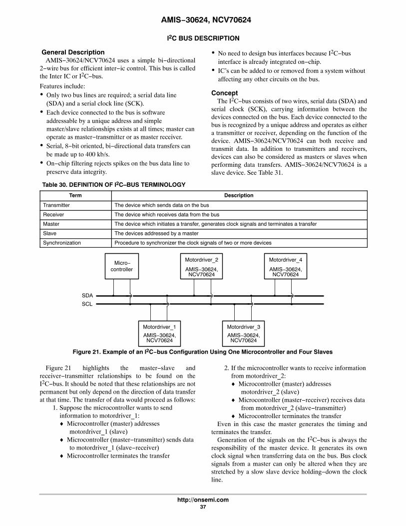
AMIS−30624, NCV70624
http://onsemi.com37
I2C BUS DESCRIPTION
General DescriptionAMIS−30624/NCV70624 uses a simple bi−directional
2−wire bus for efficient inter−ic control. This bus is calledthe Inter IC or I2C−bus.
Features include: Only two bus lines are required; a serial data line
(SDA) and a serial clock line (SCK). Each device connected to the bus is software
addressable by a unique address and simplemaster/slave relationships exists at all times; master canoperate as master−transmitter or as master receiver.
Serial, 8−bit oriented, bi−directional data transfers canbe made up to 400 kb/s.
On−chip filtering rejects spikes on the bus data line topreserve data integrity.
No need to design bus interfaces because I2C−businterface is already integrated on−chip.
IC’s can be added to or removed from a system withoutaffecting any other circuits on the bus.
ConceptThe I2C−bus consists of two wires, serial data (SDA) and
serial clock (SCK), carrying information between thedevices connected on the bus. Each device connected to thebus is recognized by a unique address and operates as eithera transmitter or receiver, depending on the function of thedevice. AMIS−30624/NCV70624 can both receive andtransmit data. In addition to transmitters and receivers,devices can also be considered as masters or slaves whenperforming data transfers. AMIS−30624/NCV70624 is aslave device. See Table 31.
Table 30. DEFINITION OF I2C–BUS TERMINOLOGY
Term Description
Transmitter The device which sends data on the bus
Receiver The device which receives data from the bus
Master The device which initiates a transfer, generates clock signals and terminates a transfer
Slave The devices addressed by a master
Synchronization Procedure to synchronizer the clock signals of two or more devices
Micro−controller
Motordriver_1
AMIS−30624,
Motordriver_2
AMIS−30624,
Motordriver_3
AMIS−30624,
Motordriver_4
AMIS−30624,
SDA
SCL
NCV70624 NCV70624
Figure 21. Example of an I2C−bus Configuration Using One Microcontroller and Four Slaves
NCV70624 NCV70624
Figure 21 highlights the master−slave andreceiver−transmitter relationships to be found on theI2C−bus. It should be noted that these relationships are notpermanent but only depend on the direction of data transferat that time. The transfer of data would proceed as follows:
1. Suppose the microcontroller wants to sendinformation to motordriver_1: Microcontroller (master) addresses
motordriver_1 (slave) Microcontroller (master−transmitter) sends data
to motordriver_1 (slave−receiver) Microcontroller terminates the transfer
2. If the microcontroller wants to receive informationfrom motordriver_2: Microcontroller (master) addresses
motordriver_2 (slave) Microcontroller (master−receiver) receives data
from motordriver_2 (slave−transmitter) Microcontroller terminates the transfer
Even in this case the master generates the timing andterminates the transfer.
Generation of the signals on the I2C−bus is always theresponsibility of the master device. It generates its ownclock signal when transferring data on the bus. Bus clocksignals from a master can only be altered when they arestretched by a slow slave device holding−down the clockline.

AMIS−30624, NCV70624
http://onsemi.com38
General Characteristics
Serial Clock Line
Serial Data Line
Rp
+5 V
Clock IN
Clock OUT
Data IN
Data OUT
AMIS−30624,
SDASCK SCL SDA
Clock IN
Clock OUT
Data IN
Data OUT
MASTER
Rp
2 1
Figure 22. Connection of a Device to the I2C−bus
NCV70624
Both SDA and SCK are bi−directional lines connected toa positive supply voltage via a pull−up resistor (seeFigure 22). When the bus is free both lines are HIGH. Theoutput stages of the devices connected to the bus must havean open drain to perform the wired−AND function. Data onthe I2C−bus can be transferred up to 400 kb/s in fast mode.The number of interfaces connected to the bus is dependenton the maximum bus capacitance limit (See CB in Table 6)and the available number of addresses.
Bit TransferThe levels for logic ‘0’ (LOW) and ‘1’ (HIGH) are not
fixed in the I2C standard but dependent on the used VDDlevel. Using AMIS−30624/NCV70624, the levels arespecified in Table 5. One clock pulse is generated for eachdata bit transferred.
Data ValidityThe data on the SDA line must be stable during the HIGH
period of the clock. The HIGH or LOW state of the data linecan only change when the clock signal on the SCL line isLOW (See Figure 23).
SCK
Data line stable−> Data valid
SDA
Change ofdata allowed
Figure 23. Bit Transfer on the I2C−bus
START and STOP ConditionsWithin the procedure of the I2C−bus, unique situations
arise, which are defined as START (S) and STOP (P)conditions (See Figure 24).
A HIGH to LOW transition on the SDA line while SCKis HIGH is one such unique case. This situation indicates aSTART condition. LOW to HIGH transition on the SDA linewhile SCK is HIGH defines a STOP condition.
START and STOP conditions are always generated by themaster. The bus is considered to be busy after the STARTcondition. The bus is considered to be free again a certaintime after the STOP condition. The bus free situation isspecified as tBUF in Table 6.
The bus stays busy if a repeated START (Sr) is generatedinstead of a STOP condition. In this respect, the START (S)and repeated START (Sr) conditions are functionallyidentical (See Figure 25). The symbol S will be used torepresent START and repeated START, unless otherwisenoted.
START STOP
SCK
STARTcondition
STOPcondition
SDA
Figure 24. START and STOP Conditions

AMIS−30624, NCV70624
http://onsemi.com39
Transferring Data
Byte FormatEvery byte put on the SDA line must be 8−bits long. The
number of bytes that can be transmitted per transfer toAMIS−30624/NCV70624 is restricted to eight. Each bytehas to be followed by an acknowledge bit. Data is transferred
with the most significant bit (MSB) first (See Figure 25). Ifa slave can’t receive or transmit another complete byte ofdata, it can hold the clock line SCK LOW to force the masterinto a wait state. Data transfer then continues when the slaveis ready for another byte of data and releases clock line SCK.
SDA
START STOP
SCK
1 2 7 8 9 1 2 3−8 9
Acknowledgementsignal from slave
Clock line heldlow by slave
Aknowledge relatedclock puse from master
STARTcondition
ACK
MSB
STOPcondition
Figure 25. Data Transfer on the I2C−bus
AcknowledgeData transfer with acknowledge is obligatory. The
acknowledge−related clock pulse is generated by the master.The transmitter releases the SDA line (HIGH) during theacknowledge clock pulse. The receiver must pull down theSDA line during the acknowledge clock pulse so that itremains stable LOW during the HIGH period of this clockpulse (see Figure 26). Of course, set−up and hold times mustalso taken into account (see Table 6). WhenAMIS−30624/NCV60624 doesn’t acknowledge the slaveaddress, the data line will be left HIGH. The master can thangenerate either a STOP condition to abort the transfer, or arepeated START condition to start a new transfer.
If AMIS−30624/NCV60624 as slave−receiver doesacknowledge the slave address but later in the transfercannot receive any more data bytes, this is indicated bygenerating a not−acknowledge on the first byte to follow.The master generates than a STOP or a repeated STARTcondition.
If a master−receiver is involved in the transfer, it mustsignal the end of data to the slave−transmitter by notgenerating an acknowledge on the last byte that was clockedout of the slave. AMIS−30624/NCV70624 asslave−transmitter shall release the data line to allow themaster to generate STOP or repeated START condition.
SDA by mastertransmitter
START
SCK frommaster
1 2 8 9
Master releases the Data line
Slave pulls data linelow if Acknowledged
Aknowledge relatedclock puse from master
STARTcondition
Acknowledged
MSB
SDA by slavereceiver
Not acknowledged
Figure 26. Acknowledge on the I2C−bus

AMIS−30624, NCV70624
http://onsemi.com40
Clock GenerationThe master generates the clock on the SCK line to transfer
messages on the I2C−bus. Data is only valid during theHIGH period of the clock.
Data Formats with 7−bit AddressesData transfers follow the format shown in Figure 27. After
the START condition (S), a slave address is sent. This
address is 7−bit long followed by an eighth bit which is a datadirection bit (R/W) − a ‘zero’ indicates a transmission(WRITE), a ‘one’ indicates a request for data (READ). Adata transfer is always terminated by a STOP condition (P)generated by the master.
START STOP
SCK
STARTcondition
STOPcondition
1 − 7 8 9 1 − 7 8 9 1 − 7 8 9
ACKR/WADDRESS DATA ACK DATA ACK
SDA
Figure 27. A Complete Data Transfer
However, if a master still wishes to communicate on thebus, it can generate a repeated START (Sr) and addressanother slave without first generating a STOP condition.Various combinations of read/write formats are thenpossible within such a transfer.
Data Transfer FormatsWriting Data to AMIS−30624/NCV70624
When writing to AMIS−30624/NCV70624, themaster−transmitter transmits to slave−receiver and thetransfer direction is not changed. A complete transmissionconsists of:
Start condition
The slave address (7−bit) Read/Write bit (‘0’ = write) Acknowledge bit Any further data bytes are followed by an
acknowledge bit. The acknowledge bit is used tosignal a correct reception of the data to thetransmitter. In this case theAMIS−30624/NCV70624 pulls the SDA line to ‘0’.The AMIS−30624/NCV70624 reads the incomingdata at SDA on every rising edge of the SCK signal
Stop condition to finish the transmission
N bytes + Acknowledge
Master to AMIS−30624
AMIS−30624 to Master
S = Start conditionP = Stop conditionA = Acknowledge (SDA = LOW)A = No Acknowledge (SDA = HIGH)
S Slave Address R/W A Data A Data A P
”0” = WRITE
Figure 28. Master Writing Data to AMIS−30624/NCV70624
Some commands for the AMIS−30624/NCV70624 aresupporting eight bytes of data, other commands aretransmitting two bytes of data. See Table 31.
Reading Data to AMIS−30624/NCV70624When reading data from AMIS−30624/NCV70624 two
transmissions are needed:
1. The first transmission consists of two bytes ofdata: The first byte contains the slave address and the
write bit. The second byte contains the address of an
internal register in the AMIS−30624/NCV70624. This internal register address is stored in the circuit RAM.
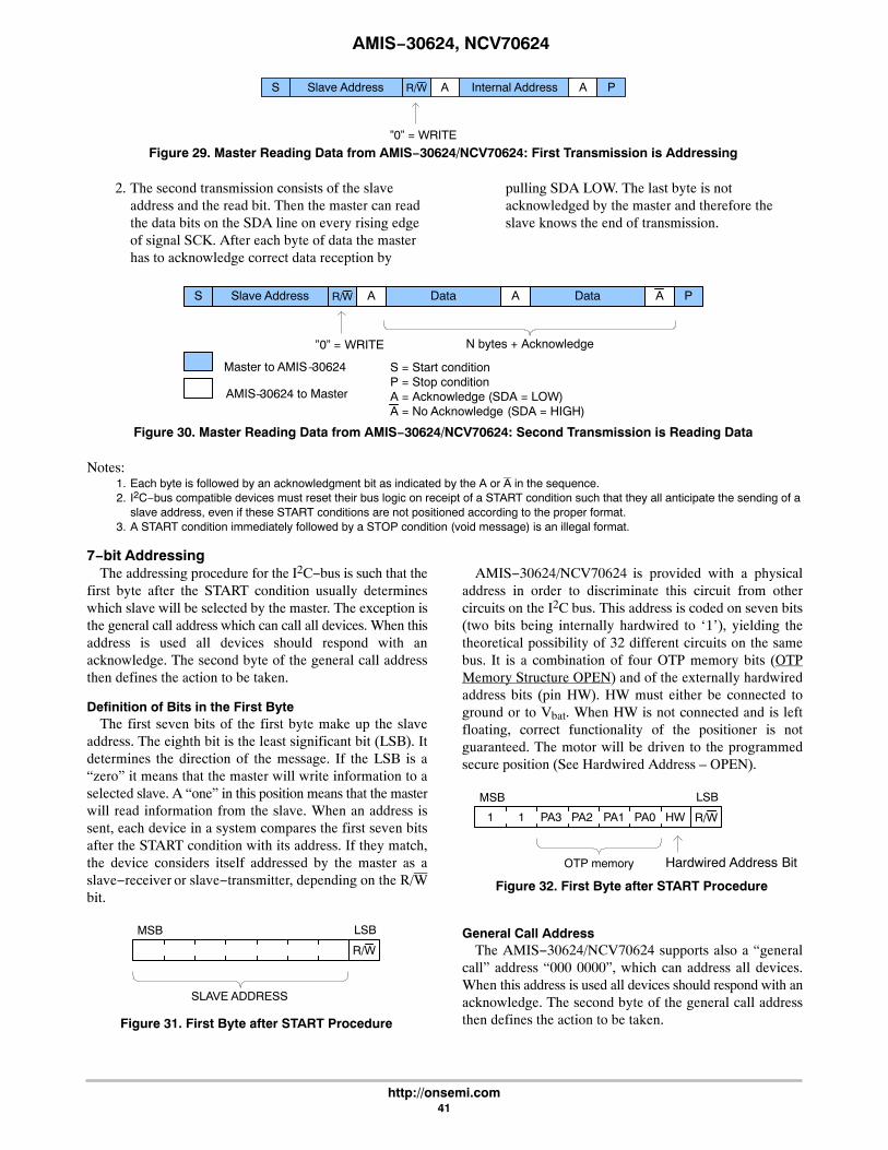
AMIS−30624, NCV70624
http://onsemi.com41
S Slave Address R/W A Internal Address
”0” = WRITE
A P
Figure 29. Master Reading Data from AMIS−30624/NCV70624: First Transmission is Addressing
2. The second transmission consists of the slaveaddress and the read bit. Then the master can readthe data bits on the SDA line on every rising edgeof signal SCK. After each byte of data the masterhas to acknowledge correct data reception by
pulling SDA LOW. The last byte is notacknowledged by the master and therefore theslave knows the end of transmission.
N bytes + Acknowledge
Master to AMIS−30624
AMIS−30624 to Master
S = Start conditionP = Stop conditionA = Acknowledge (SDA = LOW)A = No Acknowledge (SDA = HIGH)
S Slave Address R/W A Data A Data A P
”0” = WRITE
Figure 30. Master Reading Data from AMIS−30624/NCV70624: Second Transmission is Reading Data
Notes:1. Each byte is followed by an acknowledgment bit as indicated by the A or A in the sequence.2. I2C−bus compatible devices must reset their bus logic on receipt of a START condition such that they all anticipate the sending of a
slave address, even if these START conditions are not positioned according to the proper format.3. A START condition immediately followed by a STOP condition (void message) is an illegal format.
7−bit AddressingThe addressing procedure for the I2C−bus is such that the
first byte after the START condition usually determineswhich slave will be selected by the master. The exception isthe general call address which can call all devices. When thisaddress is used all devices should respond with anacknowledge. The second byte of the general call addressthen defines the action to be taken.
Definition of Bits in the First ByteThe first seven bits of the first byte make up the slave
address. The eighth bit is the least significant bit (LSB). Itdetermines the direction of the message. If the LSB is a“zero” it means that the master will write information to aselected slave. A “one” in this position means that the masterwill read information from the slave. When an address issent, each device in a system compares the first seven bitsafter the START condition with its address. If they match,the device considers itself addressed by the master as aslave−receiver or slave−transmitter, depending on the R/Wbit.
R/W
MSB LSB
SLAVE ADDRESS
Figure 31. First Byte after START Procedure
AMIS−30624/NCV70624 is provided with a physicaladdress in order to discriminate this circuit from othercircuits on the I2C bus. This address is coded on seven bits(two bits being internally hardwired to ‘1’), yielding thetheoretical possibility of 32 different circuits on the samebus. It is a combination of four OTP memory bits (OTPMemory Structure OPEN) and of the externally hardwiredaddress bits (pin HW). HW must either be connected toground or to Vbat. When HW is not connected and is leftfloating, correct functionality of the positioner is notguaranteed. The motor will be driven to the programmedsecure position (See Hardwired Address – OPEN).
R/W
MSB LSB
OTP memory
1 1 PA3 PA2 PA1 PA0 HW
Hardwired Address Bit
Figure 32. First Byte after START Procedure
General Call AddressThe AMIS−30624/NCV70624 supports also a “general
call” address “000 0000”, which can address all devices.When this address is used all devices should respond with anacknowledge. The second byte of the general call addressthen defines the action to be taken.

AMIS−30624, NCV70624
http://onsemi.com42
I2C APPLICATION COMMANDS
Introduction
Communications between the AMIS−30624/NCV70624and a 2−wire serial bus interface master takes place via alarge set of commands.
Reading commands are used to: Get actual status information, e.g. error flags Get actual position of the stepper motor Verify the right programming and configuration of
the AMIS−30624/NCV70624.
Writing commands are used to: Program the OTP memory Configure the positioner with motion parameters
(max/min speed, acceleration, stepping mode, etc.) Provide target positions to the Stepper motor
The I2C−bus master will have to use commands to managethe different application tasks the AMIS−30624/NCV70624can feature. The commands summary is given in Table 31.
Commands Table
Table 31. I2C COMMANDS WITH CORRESPONDING ROM POINTER
Command Mnemonic Function
Command Byte
Binary Hexadecimal
GetFullStatus1 Returns complete status of the chip “1000 0001” 0x81
GetFullStatus2 Returns actual, target and secure position “1111 1100” 0xFC
GetOTPParam Returns OTP parameter “1000 0010” 0x82
GotoSecurePosition Drives motor to secure position “1000 0100” 0x84
HardStop Immediate full stop “1000 0101” 0x85
ResetPosition Sets actual position to zero “1000 0110” 0x86
ResetToDefault Overwrites the chip RAM with OTP contents “1000 0111” 0x87
SetDualPosition Drives the motor to two different positions withdifferent speed
“1000 1000” 0x88
SetMotorParam Sets motor parameter “1000 1001” 0x89
SetOTP Zaps the OTP memory “1001 0000” 0x90
SetPosition Programs a target and secure position “1000 1011” 0x8B
SetStallParam Sets stall parameters “1001 0110” 0x96
SoftStop Motor stopping with deceleration phase “1000 1111” 0x8F
Runvelocity Drives motor continuously “1001 0111” 0x97
TestBemf Outputs Bemf voltage on pin SWI “1001 1111” 0x9F
These commands are described hereafter, with theircorresponding I2C frames. Refer to Data Transfer Formatsfor more details. A color coding is used to distinguish
between master and slave parts within the frames. Anexample is shown below.
Figure 33. Color Code Used in the Definition of I2C Frames
Light Gray: Master Data
White: Slave Response

AMIS−30624, NCV70624
http://onsemi.com43
Application Commands
GetFullStatus1This command is provided to the circuit by the master to
get a complete status of the circuit and of the stepper motor.Refer to Tables 19 and 20 to see the meaning of theparameters sent back to the I2C master.
Note: A GetFullStatus1 command will attempt toreset flags <TW>, <TSD>, <UV2>, <ElDef>,<StepLoss>, <CPFail>, <OVC1>, <OVC2>, and<VddReset>.
GetFullStatus1 corresponds to the following I2C command frame:
Table 32. GetFullStatus1 COMMAND FRAME
Byte Content
Structure
Bit 7 Bit 6 Bit 5 Bit 4 Bit 3 Bit 2 Bit 1 Bit 0
0 Address 1 1 OTP3 OTP2 OTP1 OTP0 HW 0
1 Command 1 0 0 0 0 0 0 1
Table 33. GetFullStatus1 RESPONSE FRAME
Byte Content
Structure
Bit 7 Bit 6 Bit 5 Bit 4 Bit 3 Bit 2 Bit 1 Bit 0
0 Address 1 1 OTP3 OTP2 OTP1 OTP0 HW 1
1 Address 1 1 1 OTP3 OTP2 OTP1 OTP0 HW
2 Data 1 Irun[3:0] Ihold[3:0]
3 Data 2 Vmax[3:0] Vmin[3:0]
4 Data 3 AccShape StepMode[1:0] Shaft Acc[3:0]
5 Data 4 VddReset StepLoss ElDef UV2 TSD TW Tinfo[1:0]
6 Data 5 Motion[2:0] ESW OVC1 OVC2 Stall CPFail
7 Data 6 1 1 1 1 1 1 1 1
8 Data 7 AbsThr[3:0] DelThr[3:0]
Where:OTP(n) OTP address bits PA[3:0]
HW Hardwired address bit
Irun[3:0] Operating current in the motor coil
Ihold[3:0] Standstill current in the motor coil
Vmax[3:0] Maximum velocity
Vmin[3:0] Minimum velocity
AccShape Enables motion without acceleration
StepMode[1:0] Step mode definition
Shaft Direction of movement
Acc[3:0] Acceleration form minimum to maximum velocity
VddReset Reset of digital supply
StepLoss Step loss occurred
ElDef Electrical defect
UV2 Battery under voltage detected
TSD Thermal shutdown
TW Thermal warning
Tinfo[1:0] Temperature Info
Motion[2:0] Motion status
ESW External switch status
OVC1 Over current in X−coil detected
OVC2 Over current in Y−coil detected
Stall Stall detected
CPFail Charge pump failure
AbsThr[3:0] Stall detection absolute threshold
DelThr[3:0] Stall detection delta threshold

AMIS−30624, NCV70624
http://onsemi.com44
GetFullStatus2This command is provided to the circuit by the master to
get the actual, target and secure position of the steppermotor. Both the actual and target position are returned insigned two’s complement 16−bit format. Secure position iscoded in 10−bit format. According to the programmed
stepping mode the LSBs of ActPos[15:0] andTagPos[15:0] may have no meaning and should beassumed to be ‘0’. This command also gives additionalinformation concerning stall detection. Refer to Tables 19and 20 to see the meaning of the parameters sent back to theI2C master.
GetFullStatus2 corresponds to the following I2C command frame:
Table 34. GetFullStatus2 COMMAND FRAME
Byte Content
Structure
Bit 7 Bit 6 Bit 5 Bit 4 Bit 3 Bit 2 Bit 1 Bit 0
0 Address 1 1 OTP3 OTP2 OTP1 OTP0 HW 0
1 Command 1 1 1 1 1 1 0 0
Table 35. GetFullStatus2 RESPONSE FRAME
Byte Content
Structure
Bit 7 Bit 6 Bit 5 Bit 4 Bit 3 Bit 2 Bit 1 Bit 0
0 Address 1 1 OTP3 OTP2 OTP1 OTP0 HW 1
1 Address 1 1 1 OTP3 OTP2 OTP1 OTP0 HW
2 Data 1 ActPos[15:8]
3 Data 2 ActPos[7:0]
4 Data 3 TagPos[15:8]
5 Data 4 TagPos[7:0]
6 Data 5 SecPos[7:0]
7 Data 6 FS2StallEn[2:0] 1 DC100 SecPos[10:8]
8 Data 7 AbsStall DelStallLo DelStallHi MinSamples[2:0] DC100StEn PWMJEn
Where:OTP(n) OTP address bits PA[3:0]
HW Hardwired address bit
ActPos[15:0] Actual position
TagPos[15:0] Target position
SecPos[10:0] Secure position
FS2StallEn[2:0] Number of full steps after stall detectionis enabled
DC100 Flag indicating PWM is at 100 percent duty cycle
AbsStall Stall detected because the absolute threshold is not reached
DelStallLo Stall detected because the delta thresholdis under crossed
DelStallHi: Stall detected because the delta thresholdis crossed
MinSamples[2:0] Back−emf sampling delay time
DC100StEn Enables the switch off of stall detection when DC100 = 1
PWMJEn PWM jitter enable
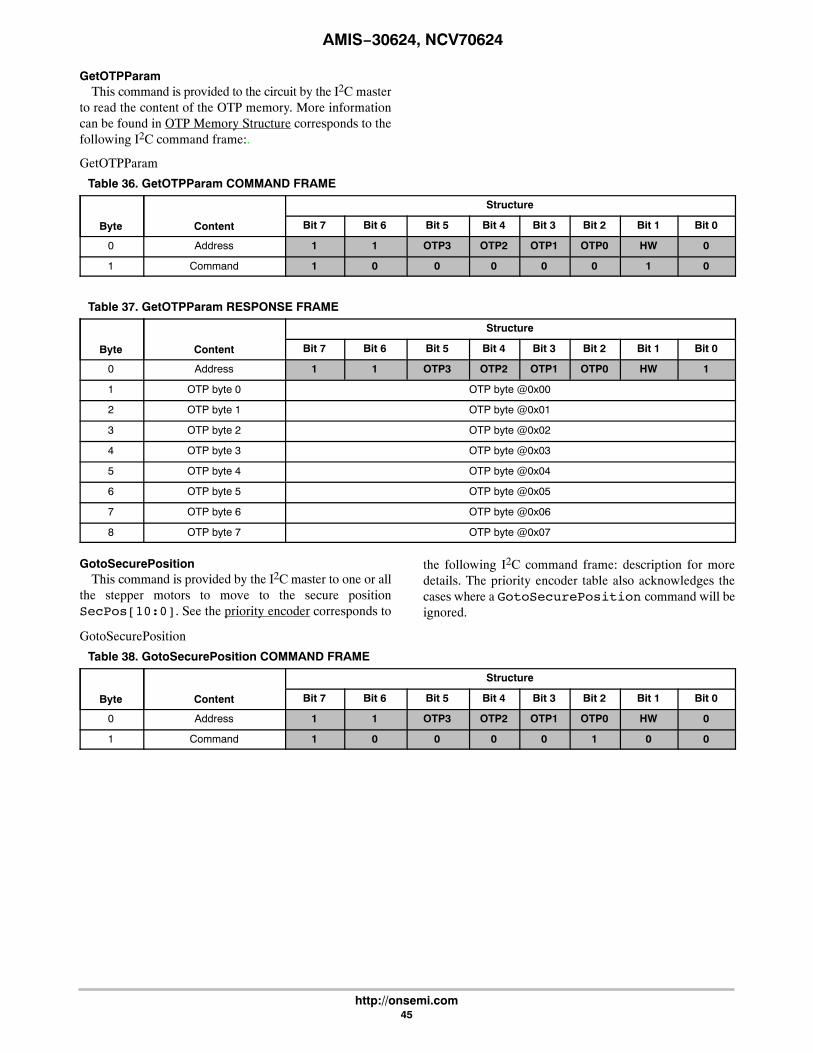
AMIS−30624, NCV70624
http://onsemi.com45
GetOTPParamThis command is provided to the circuit by the I2C master
to read the content of the OTP memory. More informationcan be found in OTP Memory Structure corresponds to thefollowing I2C command frame:.
GetOTPParam
Table 36. GetOTPParam COMMAND FRAME
Byte Content
Structure
Bit 7 Bit 6 Bit 5 Bit 4 Bit 3 Bit 2 Bit 1 Bit 0
0 Address 1 1 OTP3 OTP2 OTP1 OTP0 HW 0
1 Command 1 0 0 0 0 0 1 0
Table 37. GetOTPParam RESPONSE FRAME
Byte Content
Structure
Bit 7 Bit 6 Bit 5 Bit 4 Bit 3 Bit 2 Bit 1 Bit 0
0 Address 1 1 OTP3 OTP2 OTP1 OTP0 HW 1
1 OTP byte 0 OTP byte @0x00
2 OTP byte 1 OTP byte @0x01
3 OTP byte 2 OTP byte @0x02
4 OTP byte 3 OTP byte @0x03
5 OTP byte 4 OTP byte @0x04
6 OTP byte 5 OTP byte @0x05
7 OTP byte 6 OTP byte @0x06
8 OTP byte 7 OTP byte @0x07
GotoSecurePositionThis command is provided by the I2C master to one or all
the stepper motors to move to the secure positionSecPos[10:0]. See the priority encoder corresponds to
the following I2C command frame: description for moredetails. The priority encoder table also acknowledges thecases where a GotoSecurePosition command will beignored.
GotoSecurePosition
Table 38. GotoSecurePosition COMMAND FRAME
Byte Content
Structure
Bit 7 Bit 6 Bit 5 Bit 4 Bit 3 Bit 2 Bit 1 Bit 0
0 Address 1 1 OTP3 OTP2 OTP1 OTP0 HW 0
1 Command 1 0 0 0 0 1 0 0

AMIS−30624, NCV70624
http://onsemi.com46
HardStopThis command will be internally triggered when an
electrical problem is detected in one or both coils, leading toshutdown mode. If this occurs while the motor is moving,the <StepLoss> flag is raised to allow warning of the I2C
master at the next GetStatus1 command that steps mayhave been lost. Once the motor is stopped, ActPos registeris copied into TagPos register to ensure keeping the stopposition. The I2C master for some safety reasons can alsoissue a HardStop command.
HardStop corresponds to the following I2C command frame:
Table 39. HardStop COMMAND FRAME
Byte Content
Structure
Bit 7 Bit 6 Bit 5 Bit 4 Bit 3 Bit 2 Bit 1 Bit 0
0 Address 1 1 OTP3 OTP2 OTP1 OTP0 HW 0
1 Command 1 0 0 0 0 1 0 1
ResetPositionThis command is provided to the circuit by the I2C master
to reset ActPos and TagPos registers to zero. This can behelpful to prepare for instance a relative positioning.
ResetPosition corresponds to the following I2C command frame:
Table 40. ResetPosition COMMAND FRAME
Byte Content
Structure
Bit 7 Bit 6 Bit 5 Bit 4 Bit 3 Bit 2 Bit 1 Bit 0
0 Address 1 1 OTP3 OTP2 OTP1 OTP0 HW 0
1 Command 1 0 0 0 0 1 1 0
ResetToDefaultThis command is provided to the circuit by the I2C master
in order to reset the whole slave node into the initial state.ResetToDefault will, for instance, overwrite the RAMwith the reset state of the registers parameters (see Table 19).This is another way for the I2C master to initialize a slavenode in case of emergency, or simply to refresh the RAMcontent.
Note: ActPos and TagPos are not modified by aResetToDefault command.
Important: Care should be taken not to send aResetToDefault command while a motion is ongoing,since this could modify the motion parameters in a wayforbidden by the position controller.
ResetToDefault corresponds to the following I2C command frame:
Table 41. ResetToDefault COMMAND FRAME
Byte Content
Structure
Bit 7 Bit 6 Bit 5 Bit 4 Bit 3 Bit 2 Bit 1 Bit 0
0 Address 1 1 OTP3 OTP2 OTP1 OTP0 HW 0
1 Command 1 0 0 0 0 1 1 1
RunVelocityThis command is provided to the circuit by the I2C master
in order to put the motor in continuous motion state.
RunVelocity corresponds to the following I2C command frame:
Table 42. RunVelocity COMMAND FRAME
Byte Content
Structure
Bit 7 Bit 6 Bit 5 Bit 4 Bit 3 Bit 2 Bit 1 Bit 0
0 Address 1 1 OTP3 OTP2 OTP1 OTP0 HW 0
1 Command 1 0 0 1 0 1 1 1
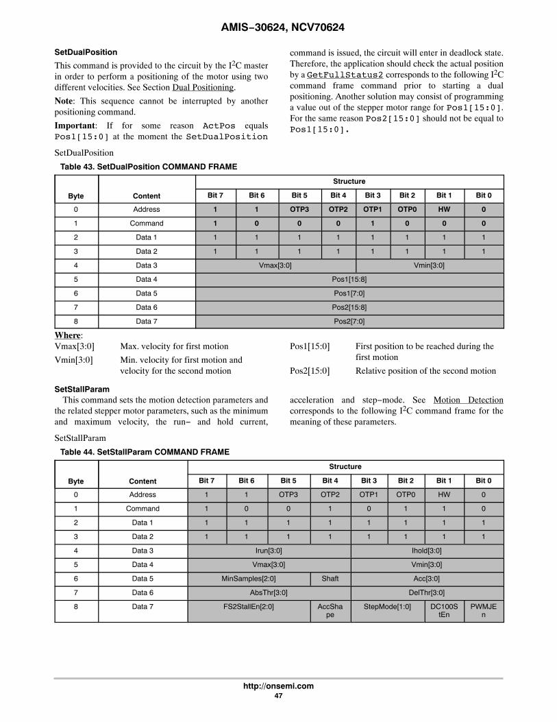
AMIS−30624, NCV70624
http://onsemi.com47
SetDualPosition
This command is provided to the circuit by the I2C masterin order to perform a positioning of the motor using twodifferent velocities. See Section Dual Positioning.
Note: This sequence cannot be interrupted by anotherpositioning command.
Important: If for some reason ActPos equalsPos1[15:0] at the moment the SetDualPosition
command is issued, the circuit will enter in deadlock state.Therefore, the application should check the actual positionby a GetFullStatus2 corresponds to the following I2Ccommand frame command prior to starting a dualpositioning. Another solution may consist of programminga value out of the stepper motor range for Pos1[15:0].For the same reason Pos2[15:0] should not be equal toPos1[15:0].
SetDualPosition
Table 43. SetDualPosition COMMAND FRAME
Byte Content
Structure
Bit 7 Bit 6 Bit 5 Bit 4 Bit 3 Bit 2 Bit 1 Bit 0
0 Address 1 1 OTP3 OTP2 OTP1 OTP0 HW 0
1 Command 1 0 0 0 1 0 0 0
2 Data 1 1 1 1 1 1 1 1 1
3 Data 2 1 1 1 1 1 1 1 1
4 Data 3 Vmax[3:0] Vmin[3:0]
5 Data 4 Pos1[15:8]
6 Data 5 Pos1[7:0]
7 Data 6 Pos2[15:8]
8 Data 7 Pos2[7:0]
Where:Vmax[3:0] Max. velocity for first motion
Vmin[3:0] Min. velocity for first motion and velocity for the second motion
Pos1[15:0] First position to be reached during the first motion
Pos2[15:0] Relative position of the second motion
SetStallParamThis command sets the motion detection parameters and
the related stepper motor parameters, such as the minimumand maximum velocity, the run− and hold current,
acceleration and step−mode. See Motion Detectioncorresponds to the following I2C command frame for themeaning of these parameters.
SetStallParam
Table 44. SetStallParam COMMAND FRAME
Byte Content
Structure
Bit 7 Bit 6 Bit 5 Bit 4 Bit 3 Bit 2 Bit 1 Bit 0
0 Address 1 1 OTP3 OTP2 OTP1 OTP0 HW 0
1 Command 1 0 0 1 0 1 1 0
2 Data 1 1 1 1 1 1 1 1 1
3 Data 2 1 1 1 1 1 1 1 1
4 Data 3 Irun[3:0] Ihold[3:0]
5 Data 4 Vmax[3:0] Vmin[3:0]
6 Data 5 MinSamples[2:0] Shaft Acc[3:0]
7 Data 6 AbsThr[3:0] DelThr[3:0]
8 Data 7 FS2StallEn[2:0] AccShape
StepMode[1:0] DC100StEn
PWMJEn

AMIS−30624, NCV70624
http://onsemi.com48
SetMotorParamThis command is provided to the circuit by the I2C master
to set the values for the stepper motor parameters (listedbelow) in RAM. Refer to Table 19 to see the meaning of theparameters sent by the I2C master.
Important: If a SetMotorParam occurs while a motionis ongoing, it will modify at once the motion parameters (see
Position Controller corresponds to the following I2Ccommand frame:). Therefore the application should notchange parameters other than Vmax while a motion isrunning, otherwise correct positioning cannot beguaranteed.
SetMotorParam
Table 45. SetMotorParam COMMAND FRAME
Byte Content
Structure
Bit 7 Bit 6 Bit 5 Bit 4 Bit 3 Bit 2 Bit 1 Bit 0
0 Address 1 1 OTP3 OTP2 OTP1 OTP0 HW 0
1 Command 1 0 0 0 1 0 0 1
2 Data 1 1 1 1 1 1 1 1 1
3 Data 2 1 1 1 1 1 1 1 1
4 Data 3 Irun[3:0] Ihold[3:0]
5 Data 4 Vmax[3:0] Vmin[3:0]
6 Data 5 SecPos[10:8] Shaft Acc[3:0]
7 Data 6 SecPos[7:0]
8 Data 7 1 PWMfreq
1 AccShape
StepMode[1:0] 1 PWMJEn
SetOTPParamThis command is provided to the circuit by the I2C master
to program and zap the OTP data D[7:0] in OTP addressOTPA[2:0].
Important: This command must be sent under a specificVBB voltage value. See parameter VBBOTP in Table 5. Thisis a mandatory condition to ensure reliable zapping.
SetOTPParam corresponds to the following I2C command frame:
Table 46. SetOTPParam COMMAND FRAME
Byte Content
Structure
Bit 7 Bit 6 Bit 5 Bit 4 Bit 3 Bit 2 Bit 1 Bit 0
0 Address 1 1 OTP3 OTP2 OTP1 OTP0 HW 0
1 Command 1 0 0 1 0 0 0 0
2 Data 1 1 1 1 1 1 1 1 1
3 Data 2 1 1 1 1 1 1 1 1
4 Data 3 1 1 1 1 1 OTPA[2:0]
5 Data 4 D[7:0]
Where:OTPA[2:0]: OTP addressD[7:0]: Corresponding OTP data

AMIS−30624, NCV70624
http://onsemi.com49
SetPositionThis command is provided to the circuit by the I2C masterto drive the motor to a given absolute position. SeePositioning (see Priority Encoder) for more details. The
priority encoder table acknowledges the cases where aSetPosition command will be ignored.
SetPosition corresponds to the following I2C command frame:
Table 47. SetPosition COMMAND FRAME
Byte Content
Structure
Bit 7 Bit 6 Bit 5 Bit 4 Bit 3 Bit 2 Bit 1 Bit 0
0 Address 1 1 OTP3 OTP2 OTP1 OTP0 HW 0
1 Command 1 0 0 0 1 0 1 1
2 Data 1 1 1 1 1 1 1 1 1
3 Data 2 1 1 1 1 1 1 1 1
4 Data 3 Pos[15:8]
5 Data 4 Pos[7:0]
Where:Pos [15:0] Signed 16−bit position set−point for motor.
SoftStopThis command will be internally triggered when the chip
temperature rises above the thermal shutdown threshold (seeTable 5 and the Temperature Management Section). Itprovokes an immediate deceleration to Vmin (seeMinimum Velocity corresponds to the following I2C
command frame:) followed by a stop, regardless of theposition reached. Once the motor is stopped, TagPosregister is overwritten with value in ActPos register toensure keeping the stop position. The I2C Master for somesafety reasons can also issue a SoftStop command.
SoftStop
Table 48. SoftStop COMMAND FRAME
Byte Content
Structure
Bit 7 Bit 6 Bit 5 Bit 4 Bit 3 Bit 2 Bit 1 Bit 0
0 Address 1 1 OTP3 OTP2 OTP1 OTP0 HW 0
1 Command 1 0 0 0 1 1 1 1
TestBemfThis command is provided to the circuit by the I2C master
in order to output the Bemf integrator output to the SWIoutput of the chip. Once activated, it can be stopped only
after POR. During the Bemf observation, reading of the SWIstate is internally forbidden.
TestBemf corresponds to the following I2C command frame:
Table 49. TestBemf COMMAND FRAME
Byte Content
Structure
Bit 7 Bit 6 Bit 5 Bit 4 Bit 3 Bit 2 Bit 1 Bit 0
0 Address 1 1 OTP3 OTP2 OTP1 OTP0 HW 0
1 Command 1 0 0 1 1 1 1 1
The products described herein (AMIS−30624, NCV70624) may be covered by the following U.S. patents: 7,271,993 and 7,288,956. There may be other patents pending.

QFN32, 7x7CASE 560AA
ISSUE ADATE 23 SEP 2015
MECHANICAL CASE OUTLINE
PACKAGE DIMENSIONS
ON Semiconductor and are trademarks of Semiconductor Components Industries, LLC dba ON Semiconductor or its subsidiaries in the United States and/or other countries.ON Semiconductor reserves the right to make changes without further notice to any products herein. ON Semiconductor makes no warranty, representation or guarantee regardingthe suitability of its products for any particular purpose, nor does ON Semiconductor assume any liability arising out of the application or use of any product or circuit, and specificallydisclaims any and all liability, including without limitation special, consequential or incidental damages. ON Semiconductor does not convey any license under its patent rights nor therights of others.
98AON30885EDOCUMENT NUMBER:
DESCRIPTION:
Electronic versions are uncontrolled except when accessed directly from the Document Repository.Printed versions are uncontrolled except when stamped “CONTROLLED COPY” in red.
PAGE 1 OF 2QFN32, 7X7
© Semiconductor Components Industries, LLC, 2019 www.onsemi.com

QFN32, 7x7CASE 560AA
ISSUE ADATE 23 SEP 2015
ON Semiconductor and are trademarks of Semiconductor Components Industries, LLC dba ON Semiconductor or its subsidiaries in the United States and/or other countries.ON Semiconductor reserves the right to make changes without further notice to any products herein. ON Semiconductor makes no warranty, representation or guarantee regardingthe suitability of its products for any particular purpose, nor does ON Semiconductor assume any liability arising out of the application or use of any product or circuit, and specificallydisclaims any and all liability, including without limitation special, consequential or incidental damages. ON Semiconductor does not convey any license under its patent rights nor therights of others.
98AON30885EDOCUMENT NUMBER:
DESCRIPTION:
Electronic versions are uncontrolled except when accessed directly from the Document Repository.Printed versions are uncontrolled except when stamped “CONTROLLED COPY” in red.
PAGE 2 OF 2QFN32, 7X7
© Semiconductor Components Industries, LLC, 2019 www.onsemi.com
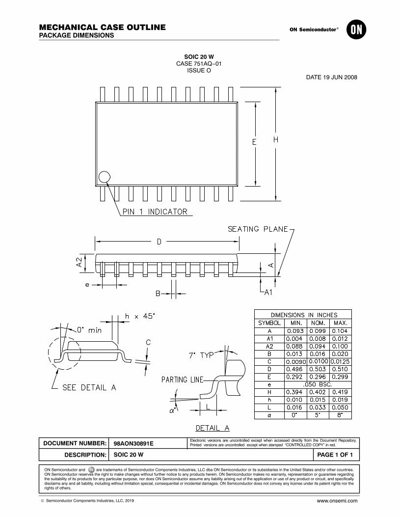
SOIC 20 WCASE 751AQ−01
ISSUE ODATE 19 JUN 2008
MECHANICAL CASE OUTLINE
PACKAGE DIMENSIONS
ON Semiconductor and are trademarks of Semiconductor Components Industries, LLC dba ON Semiconductor or its subsidiaries in the United States and/or other countries.ON Semiconductor reserves the right to make changes without further notice to any products herein. ON Semiconductor makes no warranty, representation or guarantee regardingthe suitability of its products for any particular purpose, nor does ON Semiconductor assume any liability arising out of the application or use of any product or circuit, and specificallydisclaims any and all liability, including without limitation special, consequential or incidental damages. ON Semiconductor does not convey any license under its patent rights nor therights of others.
98AON30891EDOCUMENT NUMBER:
DESCRIPTION:
Electronic versions are uncontrolled except when accessed directly from the Document Repository.Printed versions are uncontrolled except when stamped “CONTROLLED COPY” in red.
PAGE 1 OF 1SOIC 20 W
© Semiconductor Components Industries, LLC, 2019 www.onsemi.com

onsemi, , and other names, marks, and brands are registered and/or common law trademarks of Semiconductor Components Industries, LLC dba “onsemi” or its affiliatesand/or subsidiaries in the United States and/or other countries. onsemi owns the rights to a number of patents, trademarks, copyrights, trade secrets, and other intellectual property.A listing of onsemi’s product/patent coverage may be accessed at www.onsemi.com/site/pdf/Patent−Marking.pdf. onsemi reserves the right to make changes at any time to anyproducts or information herein, without notice. The information herein is provided “as−is” and onsemi makes no warranty, representation or guarantee regarding the accuracy of theinformation, product features, availability, functionality, or suitability of its products for any particular purpose, nor does onsemi assume any liability arising out of the application or useof any product or circuit, and specifically disclaims any and all liability, including without limitation special, consequential or incidental damages. Buyer is responsible for its productsand applications using onsemi products, including compliance with all laws, regulations and safety requirements or standards, regardless of any support or applications informationprovided by onsemi. “Typical” parameters which may be provided in onsemi data sheets and/or specifications can and do vary in different applications and actual performance mayvary over time. All operating parameters, including “Typicals” must be validated for each customer application by customer’s technical experts. onsemi does not convey any licenseunder any of its intellectual property rights nor the rights of others. onsemi products are not designed, intended, or authorized for use as a critical component in life support systemsor any FDA Class 3 medical devices or medical devices with a same or similar classification in a foreign jurisdiction or any devices intended for implantation in the human body. ShouldBuyer purchase or use onsemi products for any such unintended or unauthorized application, Buyer shall indemnify and hold onsemi and its officers, employees, subsidiaries, affiliates,and distributors harmless against all claims, costs, damages, and expenses, and reasonable attorney fees arising out of, directly or indirectly, any claim of personal injury or deathassociated with such unintended or unauthorized use, even if such claim alleges that onsemi was negligent regarding the design or manufacture of the part. onsemi is an EqualOpportunity/Affirmative Action Employer. This literature is subject to all applicable copyright laws and is not for resale in any manner.
PUBLICATION ORDERING INFORMATIONTECHNICAL SUPPORTNorth American Technical Support:Voice Mail: 1 800−282−9855 Toll Free USA/CanadaPhone: 011 421 33 790 2910
LITERATURE FULFILLMENT:Email Requests to: [email protected]
onsemi Website: www.onsemi.com
Europe, Middle East and Africa Technical Support:Phone: 00421 33 790 2910For additional information, please contact your local Sales Representative
◊