agilent 85190a ic-cap 2008 - ubc ecerobertor/links_files/files/iccap-2008-doc/...model parameter...
TRANSCRIPT
Agilent 85190A IC-CAP 2008
Nonlinear Device Models Volume 1
Agilent Technologies
Notices© Agilent Technologies, Inc. 2000-2008
No part of this manual may be reproduced in any form or by any means (including elec-tronic storage and retrieval or translation into a foreign language) without prior agree-ment and written consent from Agilent Technologies, Inc. as governed by United States and international copyright laws.
EditionMarch 2008
Printed in USA
Agilent Technologies, Inc.5301 Stevens Creek Blvd. Santa Clara, CA 95052 USA
WarrantyThe material contained in this docu-ment is provided “as is,” and is sub-ject to being changed, without notice, in future editions. Further, to the max-imum extent permitted by applicable law, Agilent disclaims all warranties, either express or implied, with regard to this manual and any information contained herein, including but not limited to the implied warranties of merchantability and fitness for a par-ticular purpose. Agilent shall not be liable for errors or for incidental or consequential damages in connec-tion with the furnishing, use, or per-formance of this document or of any information contained herein. Should Agilent and the user have a separate written agreement with warranty terms covering the material in this document that conflict with these terms, the warranty terms in the sep-arate agreement shall control.
Technology Licenses The hardware and/or software described in this document are furnished under a license and may be used or copied only in accor-dance with the terms of such license.
Restricted Rights LegendU.S. Government Restricted Rights. Soft-ware and technical data rights granted to the federal government include only those rights customarily provided to end user cus-tomers. Agilent provides this customary commercial license in Software and techni-cal data pursuant to FAR 12.211 (Technical Data) and 12.212 (Computer Software) and, for the Department of Defense, DFARS 252.227-7015 (Technical Data - Commercial Items) and DFARS 227.7202-3 (Rights in Commercial Computer Software or Com-puter Software Documentation).
Safety Notices
CAUTION
A CAUTION notice denotes a haz-ard. It calls attention to an operat-ing procedure, practice, or the like that, if not correctly performed or adhered to, could result in damage to the product or loss of important data. Do not proceed beyond a CAUTION notice until the indicated conditions are fully understood and met.
WARNING
A WARNING notice denotes a hazard. It calls attention to an operating procedure, practice, or the like that, if not correctly per-formed or adhered to, could result in personal injury or death. Do not proceed beyond a WARNING notice until the indicated condi-tions are fully understood and met.
AcknowledgmentsUNIX ® is a registered trademark of the Open Group.
Windows ®, MS Windows ® and Windows NT ® are U.S. registered trademarks of Microsoft Corporation.
ErrataThe IC-CAP product may contain references to “HP” or “HPEESOF” such as in file names and directory names. The business entity formerly known as “HP EEsof” is now part of Agilent Technologies and is known as “Agilent EEsof.” To avoid broken functional-ity and to maintain backward compatibility for our customers, we did not change all the names and labels that contain “HP” or “HPEESOF” references.
2 IC-CAP Nonlinear Device Models Volume 1
Contents
1 Using the MOS Modeling Packages
IC-CAP Nonlinear Device Models Vo
Key Features and Enhancements of the MOS Modeling Packages 16
Data Structure inside the MOS Modeling Packages 18
Files Resulting from Measurement and Extraction using the Modeling Packages 19
DC and CV Measurement of MOSFET’s for the MOS Models 23
Project Notes 26Temperature Setup 26Switch Matrix 27Device List 30Drain/Source – Bulk Diodes for DC Measurements 65Options 65Import Wizard 66Example Export/Import Procedure 68
RF Measurement 72
RF Measurement Notes 72RF Measurement Conditions 72De-embedding/Pad Structures 75DUTs 81RF Measurement Options 84
Extraction of DC/CV Parameters 85
DC Notes 87DC Information 87DC Initialize 89Binning 93
lume 1 3
4
DC Extract 98Plots 108Finetune 111DC HTML 113DC Options 116DC Boundaries 118
Extraction of Parameters for the RF Models 121
RF Extract Notes 122RF Extract Information 123RF Extract Initialize 123Model Parameter Sets 125RF Extract 127RF Extract Display 131RF Extract HTML 132RF Extract Options 132Circuit Files 134RF Extract Boundaries 134
2 HiSIM2 and HiSIM_HV Characterization
Modeled Device Characteristics of the HiSIM2 model 137
SPICE Model Parameters 139
RF Circuit used for HiSIM2 153
HiSIM_HV model 157
Additional SPICE Model Parameters for HiSIM_HV 162
References 164
3 PSP Characterization
Overview of the PSP model 166
Global Level 166Local Level 166Hierarchical Structure of the PSP Model 167
IC-CAP Nonlinear Device Models Volume 1
IC-CAP Nonlinear Device Models Vo
PSP Modeling Package 168
Extraction of Parameters for the PSP Model 169
Simultaneous Adjustment of Local and Global Parameters 176
Setting up the Extraction Flow to Use this Feature 181
Binning of PSP Models 188
Binning Rules in PSP 188Generation Process for a Binned Simulation Model 190
Parameters for the PSP model 197
Binning Mode 214Stress Model 228
4 BSIM4 Characterization
What’s new inside the BSIM4 Modeling Package: 232
Basic Effects Modeled in BSIM4 238
Enhanced drain current model 238RF and high-speed model 238
Key Features of the BSIM4 Modeling Package 239
DC Behavioral Modeling 240
Threshold Voltage Model 240Well-Proximity effect modeling 242Basic Threshold voltage equation 245Gate Direct Tunneling Current Model 252Drain Current Model 258Unified Mobility Model 260Drain/Source Resistance Model 262Saturation Region Output Conductance Model 264Body Current Model 269Stress Effect Modeling 270
CV Modeling 273
Capacitance Model 273
lume 1 5

6
Intrinsic Capacitance Modeling 273Intrinsic Capacitance Model Equations 276Fringing Capacitance Models 276Overlap Capacitance Model 276
Structure of the BSIM4 RF Simulation Model 280
Test Structures for Deep Submicron CMOS Processes 297
SPICE Model Parameters for BSIM4.5.0 298
Main Model Parameters 298Temperature Modeling Parameters 311Flicker Noise Model Parameters 312Stress Effect Modeling 313Well-Proximity Modeling 314High-Speed / RF Model Parameters 315Layout-Dependent Parasitics Model Parameters 317Model Selection Flags 318
References 320
5 BSIM3v3 Characterization
What’s new inside the BSIM3 Modeling Package: 321
The BSIM3 Model 327
Versions of the BSIM3 Model 328
The Unified I-V Model of BSIM3v3 330
Threshold Voltage 330Carrier Mobility Reduction 340Effective Channel Length and Width 342Drain Current 345Output Resistance 354
Substrate Current 360Drain/Bulk and Source/Bulk Diodes 362Consistency Check of DC measurement data for multiple
measured devices 364
IC-CAP Nonlinear Device Models Volume 1

IC-CAP Nonlinear Device Models Vo
Capacitance Model 368
Junction Capacitance 369Extrinsic Capacitance 374Intrinsic Capacitance 377The Overall Capacitance in BSIM3 383
High Frequency Behavior 385
Macro Model for High Frequency Application 385Single Subcircuit Model for BSIM3v3 RF Transistors 387Fully Scalable Subcircuit Model for BSIM3v3 RF Transistors
391Modeling Strategy 396
Temperature Dependence 401
Built-in Temperature Dependencies 401Temperature Effects 401
Noise Model 409
Conventional Noise Model for MOS Devices 409BSIM3v3 Noise Model 411
SPICE Model Parameters 412
Main Model Parameters 412Process Related Parameters 417Temperature Modeling Parameters 418Flicker Noise Model Parameters 418Non-Quasi-Static Model Parameters 419Model Selection Flags 419User Definable Parameters 420Additional Parameters needed for accurate RF modeling 420
Test structures for Deep Submicron CMOS Processes 422
Transistors for DC measurements 422Drain/Source – Bulk Diodes for DC Measurements 425Test Structures for CV Measurements 425Testchips 430
lume 1 7
8
Test Structures for S-parameter Measurements 431
Extraction of Model Parameters 445
Parameter Extraction Sequence 445Extraction Strategy 446
Binning of Model Parameters 452
Usage of binned models in a simulator 452Extraction of binned model parameters 456Implementation into the BSIM3/4 Modeling Packages 458
Importing older version BSIM3v3 Files 462
References 466
6 MOS Model 9 Characterization
MOS Model 9 Model 471
The MM9 Model File 473
Model Parameters 473Model Variables 476The extract DUT 484The quick_ext DUT 491The dutx DUT 496Macros 501
Parameter Extraction 505
Data Organization 507Scaling Rules 507Device Geometries 508
Optimizing 510
Optimization Transforms and Macros 510
The JUNCAP Model 513
The area, locos, and gate DUTs 513The analysis DUT 515Macros 524
IC-CAP Nonlinear Device Models Volume 1
IC-CAP Nonlinear Device Models Vo
General Extraction Methodology 527
References 530
7 UCB MOS Level 2 and 3 Characterization
UCB MOSFET Model 533
Simulators 534
MOSFET Model Parameters 535
Test Instruments 541
Instrument-to-Device Connections 541
Measuring and Extracting 543
Measurement and Extraction Guidelines 543Extracting Parameters 545Simulating 551Displaying Plots 552Optimizing 552
Extraction Algorithms 553
Classical Parameter Extractions 553Narrow-Width Parameter Extractions 553Short-Channel Parameter Extractions 554Saturation Parameter Extractions 554Sidewall and Junction Capacitance Parameter Extractions
554
HSPICE LEVEL 6 MOSFET Model 556
Model Parameters 556Measurement 558Extraction and Optimization 559
References 560
8 Bipolar Transistor Characterization
Bipolar Device Model 563
lume 1 9

10
Simulators 564
Model Parameters 565
Test Instruments 571
Instrument-to-Device Connections 571
Measuring and Extracting 573
Measurement and Extraction Guidelines 573Extracting Parameters 577
Extraction Algorithms 582
DC Parameter Extractions 582Capacitance Parameter Extractions 583Parasitic DC Parameter Extractions 583AC Parameter Extractions 584
References 586
9 Agilent-HBT Modeling Package
Key Features of the Agilent-HBT Modeling Package 589
Before You Begin 589
Requirements 589
Getting Started 590
Structure of the Modeling Package 592
Settings Window 595
Information 595Device Settings 596General Settings/Options 597
Measure Window 599
Instrument Settings 599Measurement Settings 603Pad Open/Short 605Measure DC 609
IC-CAP Nonlinear Device Models Volume 1
IC-CAP Nonlinear Device Models Vo
Measure RF 615Options for Measurements 620Exporting/Importing Measured Data 621
Extract Window 625
Simulation Settings 625Parameter Boundaries 627Extract/Optimize 629Options for Extractions 645
Agilent-HBT Model Extraction 647
Extraction Overview 647DC Extraction 647R Extraction 655CJ Extraction 656SP Extraction 656FT Extraction 656
10 UCB GaAs MESFET Characterization
UCB GaAs MESFET Model 663
Simulators 664
Model Parameters 667
Test Instruments 669
Instrument-to-Device Connections 669
Measuring and Extracting 670
Measurement and Extraction Guidelines 670Extraction Procedure Overview 673Parameter Measurement and Extraction 674Alternate Extraction Method 676Simulating 678Displaying Plots 678Optimizing 678
lume 1 11
12
Extraction Algorithms 680
Inductance and Resistance Extraction 680DC Parameter Extractions 680Capacitance Parameter Extractions 680
References 681
11 Curtice GaAs MESFET Characterization
Curtice GaAs MESFET Model 685
Simulators 686
Model Parameters 688
Test Instruments 692
Instrument-to-Device Connections 692
Measuring and Extracting 694
Measurement and Extraction Guidelines 694Extraction Procedure Overview 697Parameter Measurement and Extraction 698Alternate Extraction Method 701Simulating 703Displaying Plots 703Optimizing 703
Extraction Algorithms 704
Inductance and Resistance Extraction 704DC Parameter Extractions 704Capacitance Parameter Extractions 705
References 705
12 Circuit Modeling
Definition of an IC-CAP Circuit 708
IC-CAP Circuit Modeling Operations 709
IC-CAP Nonlinear Device Models Volume 1
IC-CAP Nonlinear Device Models Vo
Defining a Circuit 710
Supported Circuit Components 710
Circuit Measurement 713
Multiple Instrument Names 713Isolating Circuit Elements for Measurement and Extraction
713
Circuit Parameter Extraction 715
Extracting Transistor Parameters Using Library Functions 715Extracting Parameters Through Optimization 716
Circuit Simulation 719
Design Optimization 719
Test Circuits 721
Syntax 721
Hierarchical Modeling 723
Circuits Built from Sub-models 723
Functional Circuit Blocks 725
Types of Circuits in IC-CAP 725Modeling the Reverse Active Region of an NPN Transistor 725Modeling an Operational Amplifier 727
References 736
13 1/f Noise Extraction Toolkit
Types of Noise 738
The Significance of 1/f Noise 739
1/f (Flicker Noise) Modeling 740
Noise Measurement Setup 743
Parameter Extraction Procedure 745
Low pass filter 746
lume 1 13

14
1/f Noise Toolkit Description 748
System Parts List (Hardware) 748Software Requirements 748
Opening the 1/f Toolkit 749
System Settings 752
1/f Noise System Settings 752Notes 752
General Settings 754
Instrument Settings 755GUI Options 758
Verify DC 760
Measure Noise 765
1/f Noise Extraction with MOS Transistors 784
1/f Noise Function Descriptions 798
References 801
Index
IC-CAP Nonlinear Device Models Volume 1
Agilent 85190A IC-CAP 2008Nonlinear Device Models Volume 1
1Using the MOS Modeling Packages
Key Features and Enhancements of the MOS Modeling Packages 16
Data Structure inside the MOS Modeling Packages 18
DC and CV Measurement of MOSFET’s for the MOS Models 23
RF Measurement 72
Extraction of DC/CV Parameters 85
Extraction of Parameters for the RF Models 121
This chapter discusses the measurement and extraction of parameters using the MOS Modeling Packages for extracting HISIM2, BSIM3v3, BSIM4, and PSP model parameters developed by AdMOS. The Modeling Packages use similar Graphic User Interfaces (GUI). Handling of the measurement and extraction tasks using one of the Modeling Packages is similar and therefore only needs to be described once.
Model specific parts are located in Chapter 2, “HiSIM2 and HiSIM_HV Characterization Chapter 3, “PSP Characterization”, Chapter 4, “BSIM4 Characterization”, and Chapter 5, “BSIM3v3 Characterization”. Inside those chapters you will find some theoretical aspects for each of the models. Links are provided to bring you from this chapter to the respective chapters and vice versa.
15Agilent Technologies
1 Using the MOS Modeling Packages
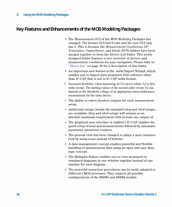
Key Features and Enhancements of the MOS Modeling Packages
16
• The Measurement GUI of the MOS Modeling Packages has changed. The former GUI had 8 tabs and the new GUI only has 5. This is because the Measurement Conditions, DC Transistor, Capacitance, and Diode DUTs folders have been merged together to form the Device List folder. This newly designed folder features a tree overview of devices and measurement conditions for easy navigation. Please refer to “Device List” on page 30 for a description of this folder.
• An important new feature is the .mdm Import Wizard, which enables you to import data measured with software other than IC-CAP that is not in IC-CAP mdm-format.
• Increased flexibility when measuring Id-Vd curves where Vd is first order sweep. The starting values of the second order sweep Vg can depend on the threshold voltage of an appropriate transconductance measurement for the same device.
• The ability to select/deselect outputs for each measurement setup.
• Additional setups, beside the standard idvg and idvd setups, are available. Idvg and idvd setups will remain as an absolute minimum requirement with at least one output id.
• The graphical user interface in Agilent‘s IC-CAP enables the quick setup of tests and measurements followed by automatic parameter extraction routines.
• The general view has been changed to adopt a more intuitive look by using icons instead of buttons.
• A data management concept enables powerful and flexible handling of measurement data using an open and easy data base concept.
• The Multiplot feature enables you to view measured or simulated diagrams in one window together instead of one window for each diagram.
• The powerful extraction procedures can be easily adopted to different CMOS processes. They support all possible configurations of the BSIM3 and BSIM4 models.
IC-CAP Nonlinear Device Models Volume 1
Using the MOS Modeling Packages 1
IC-CAP Nonlinear Device Models Vo
• Quality assurance procedures are checking every step in the modeling flow from measurements to the final export of the SPICE model parameter set.
• The fully automatic generation of HTML reports is included to enable web publishing of a modeling project.
• The modeling package supports SPICE3e2 and major commercial simulator formats such as HSPICE, Spectre, and Agilent’s ADS.
The Modeling Packages Support Measurements on
• Single-finger (normal) transistors
• Parasitic diodes
• Capacitances:
• Oxide
• Overlap
• Bulk-drain, source-drain junction
• Intrinsic
• RF multifinger transistors
The Modeling Package Supports Extractions for
• Basic transistor behavior
• Parasitic diodes
• Capacitances
• RF behavior (S-parameters)
lume 1 17
1 Using the MOS Modeling Packages
Data Structure inside the MOS Modeling Packages
18
The Modeling Packages are using a totally different, more advanced data storing concept compared to former modeling products inside IC-CAP. The drawback of recent modeling products was that measured data was always stored in model files together with transforms, macros, plot definitions, and so on.
This method has two major disadvantages:
• The additional information is stored n times and is therefore highly redundant.
IC-CAP Nonlinear Device Models Volume 1
Using the MOS Modeling Packages 1
IC-CAP Nonlinear Device Models Vo
• The combination of data and code makes it very difficult to introduce updates to the code.
Now, the new architecture of the MOS Modeling Packages overcome these disadvantages.
The measurement module contains all measurement related items like DUTs/Setups to perform measurements and setup of test and measurement conditions. The measured data is stored together with device information like gate length, pin numbers of a switch matrix used, and so forth in IC-CAP .mdm data base format. These .mdm files are organized as projects that can be identified by project name.
Now, the extraction module extracts the necessary data from stored .mdm files to perform model parameter extraction and visualization of measured and simulated results. In addition, this method enables the generation of new data representations where the scalability of a model can be easily verified.
Files Resulting from Measurement and Extraction using the Modeling Packages
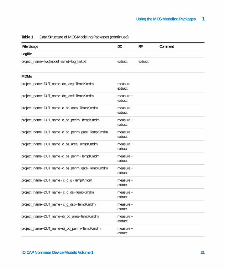
This section describes the files resulting from measurement and extraction of MOS devices using the MOS Modeling Packages. The following table shows how file names are being used. The bold printed words inside the left most column names the task the files are being used for and the normal printed names are the appropriate file names used to store the files for a specific project. The columns marked DC and RF list the task performed by each file. For example, measure+extract in the column DC means that this file is used in measurement and extraction of DC parameters.
NOTE The following characters are excluded from use in file or project names:“ / \ , . ; : * ? ~ % $ ’ ä Ä ö Ö ü Ü as well as “empty space”.
lume 1 19
1 Using the MOS Modeling Packages
Table 1 Data Structure of MOS Modeling Packages
File Usage DC RF Comment
Project search
*~dc_idvg~*K.mdm measure + extract
*~rf_s_dut~*K.mdm measure + extract
Settings
project_name~dc_meas~settings.set measure + extract
project_name~rf_meas~settings.set measure + extract
project_name~lwc(model name)~settings.set extract extract
Boundaries
*~lwc(model name)~boundaries.set extract extract default for export,* = project_name
MPS
project_name~lwc(model name).mps measure + extract
measure + extract
for scaled model
project_name~DUT_name~lwc(model name).mps extract for single model
LIB
project_name~DUT_name~Simulator~lwc(model name).lib extract for single model
project_name~Simulator~lwc(model name).lib extract extract for scaled model
20 IC-CAP Nonlinear Device Models Volume 1
Using the MOS Modeling Packages 1
Logfile
project_name~lwc(model name)~log_fail.txt extract extract
MDMs
project_name~DUT_name~dc_idvg~TempK.mdm measure + extract
project_name~DUT_name~dc_idvd~TempK.mdm measure + extract
project_name~DUT_name~c_bd_area~TempK.mdm measure + extract
project_name~DUT_name~c_bd_perim~TempK.mdm measure + extract
project_name~DUT_name~c_bd_perim_gate~TempK.mdm measure + extract
project_name~DUT_name~c_bs_area~TempK.mdm measure + extract
project_name~DUT_name~c_bs_perim~TempK.mdm measure + extract
project_name~DUT_name~c_bs_perim_gate~TempK.mdm measure + extract
project_name~DUT_name~ c_d_g~TempK.mdm measure + extract
project_name~DUT_name~ c_g_ds~TempK.mdm measure + extract
project_name~DUT_name~ c_g_dsb~TempK.mdm measure + extract
project_name~DUT_name~di_bd_area~TempK.mdm measure + extract
project_name~DUT_name~di_bd_perim~TempK.mdm measure + extract
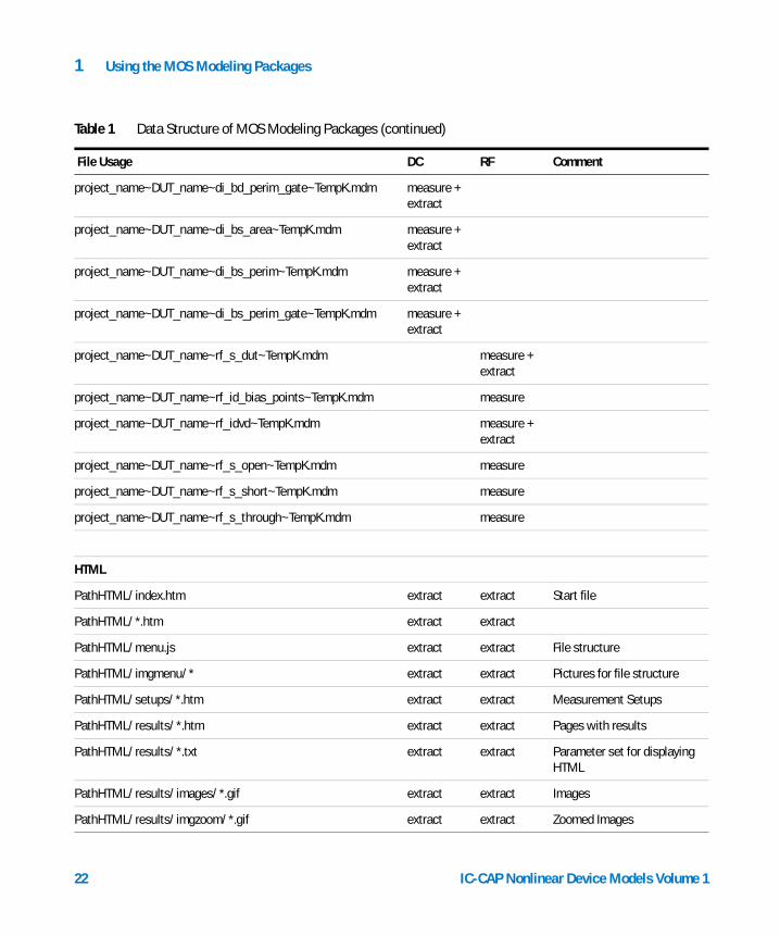
Table 1 Data Structure of MOS Modeling Packages (continued)
File Usage DC RF Comment
IC-CAP Nonlinear Device Models Volume 1 21
1 Using the MOS Modeling Packages
project_name~DUT_name~di_bd_perim_gate~TempK.mdm measure + extract
project_name~DUT_name~di_bs_area~TempK.mdm measure + extract
project_name~DUT_name~di_bs_perim~TempK.mdm measure + extract
project_name~DUT_name~di_bs_perim_gate~TempK.mdm measure + extract
project_name~DUT_name~rf_s_dut~TempK.mdm measure + extract
project_name~DUT_name~rf_id_bias_points~TempK.mdm measure
project_name~DUT_name~rf_idvd~TempK.mdm measure + extract
project_name~DUT_name~rf_s_open~TempK.mdm measure
project_name~DUT_name~rf_s_short~TempK.mdm measure
project_name~DUT_name~rf_s_through~TempK.mdm measure
HTML
PathHTML/index.htm extract extract Start file
PathHTML/*.htm extract extract
PathHTML/menu.js extract extract File structure
PathHTML/imgmenu/* extract extract Pictures for file structure
PathHTML/setups/*.htm extract extract Measurement Setups
PathHTML/results/*.htm extract extract Pages with results
PathHTML/results/*.txt extract extract Parameter set for displaying HTML
PathHTML/results/images/*.gif extract extract Images
PathHTML/results/imgzoom/*.gif extract extract Zoomed Images
Table 1 Data Structure of MOS Modeling Packages (continued)
File Usage DC RF Comment
22 IC-CAP Nonlinear Device Models Volume 1
Using the MOS Modeling Packages 1
DC and CV Measurement of MOSFET’s for the MOS Models
IC-CAP Nonlinear Device Models Vo
This section provides information to make the necessary measurements of your devices. It will provide information on features of the MOS Modeling Packages and how to use the graphic user interface (GUI). For hints on how to measure and what to measure using the right devices, see Chapter 3, “PSP Characterization, Chapter 4, “BSIM4 Characterization”, and Chapter 5, “BSIM3v3 Characterization”.
NOTE Since the measurement module of the MOS Modeling Packages are identical, we describe only one of them in detail.
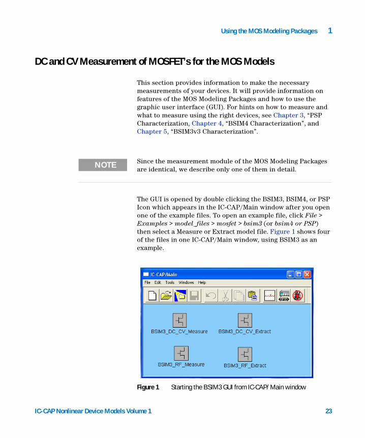
The GUI is opened by double clicking the BSIM3, BSIM4, or PSP Icon which appears in the IC-CAP/Main window after you open one of the example files. To open an example file, click File > Examples > model_files > mosfet > bsim3 (or bsim4 or PSP) then select a Measure or Extract model file. Figure 1 shows four of the files in one IC-CAP/Main window, using BSIM3 as an example.
Figure 1 Starting the BSIM3 GUI from IC-CAP/Main window
lume 1 23
24
1 Using the MOS Modeling Packages
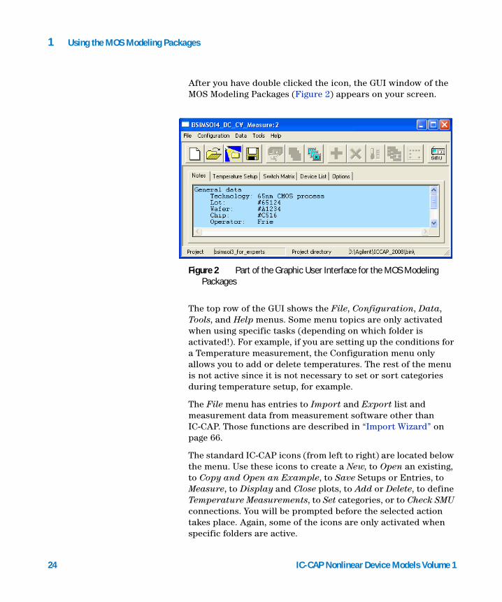
After you have double clicked the icon, the GUI window of the MOS Modeling Packages (Figure 2) appears on your screen.
The top row of the GUI shows the File, Configuration, Data, Tools, and Help menus. Some menu topics are only activated when using specific tasks (depending on which folder is activated!). For example, if you are setting up the conditions for a Temperature measurement, the Configuration menu only allows you to add or delete temperatures. The rest of the menu is not active since it is not necessary to set or sort categories during temperature setup, for example.
The File menu has entries to Import and Export list and measurement data from measurement software other than IC-CAP. Those functions are described in “Import Wizard” on page 66.
The standard IC-CAP icons (from left to right) are located below the menu. Use these icons to create a New, to Open an existing, to Copy and Open an Example, to Save Setups or Entries, to Measure, to Display and Close plots, to Add or Delete, to define Temperature Measurements, to Set categories, or to Check SMU connections. You will be prompted before the selected action takes place. Again, some of the icons are only activated when specific folders are active.
Figure 2 Part of the Graphic User Interface for the MOS Modeling Packages
IC-CAP Nonlinear Device Models Volume 1
Using the MOS Modeling Packages 1
IC-CAP Nonlinear Device Models Vo
The lower part of the window displays the project name and project directory.
To Print a setup, choose File > Print Setup. This opens a dialog box. In this dialog box, enter the command line for your specific printing device and choose OK. The folder will be printed.
NOTE On Windows operating system, the command line is print /d:<printer name>. For example, if the printer is connected to a server named MYFS1 and the printer is named MY0017, type:
print /d:'\\MYFS1\MY0017'
NOTE If you don’t enter a printer command, the output will be redirected to the IC-CAP/Status window.
From the Help menu you can choose between browsing the Topics or getting help for each of the different task folders described below. There are in depth hints for the task, for example, which device geometries to use or how to connect the instrument to the device under test to get the best extraction results from your measurements. You will find links that bring you to Chapter 3, “PSP Characterization”, Chapter 4, “BSIM4 Characterization”, or Chapter 5, “BSIM3v3 Characterization”. Use your Browsers Back button to return to the location you were at before following the link.
Below the top row of icons are five folders. Basically, each folder is assigned to a specific task in the measurement process. They are intended to be parsed from left to right, but you are not bound to that order. Some entries into one or the other folder will change settings on another folder.
For the new user: You should process the folders in the order from left to right.
Each of the following sections describe one folder of the GUI. BSIM3, BSIM4, and PSP model folders are usually equal to each other.
lume 1 25
1 Using the MOS Modeling Packages
Project Notes
26
The notes folder is provided to store notes you take on a specific project. You can enter general data like technology used to produce this wafer as well as lot, wafer, and chip number. There is a field to enter the operator’s name and the date the measurement was taken. Space has been provided to enter notes on that project.
Notes entered into the measurement module will be transferred to the Information folder inside the DC_CV_Extraction modules.
Temperature Setup
Use this folder to define measurements at specified temperatures. Basically, the measurement of all DUTs is performed at SPICE default temperature TNOM, which is set to 27° Celsius.
NOTE To change the default value of 27°C to represent your measurement temperature, double click and enter the actual environment temperature inside your measurement lab into the TNOM field.
Add new measurement temperatures using the Add icon or the Configuration menu. If you no longer need a measurement temperature, click the Delete button. You will be prompted for the temperature to be deleted. If there is a file containing measured data for this temperature, the data file will be deleted if you choose OK on the prompt dialog.
The delete window does not contain an entry for the temperature set as TNOM, since TNOM cannot be excluded from measurement and extraction.
IC-CAP Nonlinear Device Models Volume 1
Using the MOS Modeling Packages 1
NOTE Don’t forget to enter the actual temperature in degree Celsius (°C) into the TNOM field during measurement of the devices.
It is not possible to delete the nominal temperature TNOM!
IC-CAP Nonlinear Device Models Vo
When you add a new measurement temperature, a new column is added to the Device List folder’s Device List table for DC Transistor, Capacitance, and DC Diode.
Any changes on the Temperature Setup folder must be saved prior to selecting another folder.
Switch Matrix
Use this folder to define which measurements use a switch matrix (see Figure 3). There are three options: Use a switch matrix for DC Transistor Measurements, for Capacitance Measurements, and for Diode Measurements. You can select any one or more than one by checking the appropriate boxes.
NOTE If you are not using a switch matrix, leave all three check boxes unchecked. In this case, you do not have terminal assignment columns in the Transistor’s Device List table in the Device List folder. Instead, you determine the connections by wiring the appropriate SMU to the desired transistor terminal.
NOTE Assignments must use SMU1....SM4. This assignment is done inside the hardware setup of IC-CAP. Usually, the default of the appropriate DC-CV-Analyzer is SMU1...4. In rare cases, such as the Agilent E5250 for example, the default SMU number corresponds to the slot number of the module inserted into the instrument. If your E5250 uses 4 SMU’s at slot No. 1, 3, 5, 6, the default names of the SMU’s are SMU1, SMU3, SMU5 and SMU6. You must change this default names to reflect SMU1, SMU2, SMU3 and SMU4 to properly communicate with the BSIM3/4 and PSP modules.
NOTE To change or enter the names of the Source-Measurement-Units (SMU’s), open the model for editing then go to the folder DUTs/Setup, subfolder Measure/Simulate. Configure the different inputs/outputs there.
lume 1 27

28
1 Using the MOS Modeling Packages
The Basic Settings provide a choice of several different Matrix Models, which are supported by IC-CAP. Type the appropriate Bus and GPIB address of the Switch Matrix (SWM Address; 22 in our example) as well as the GPIB-Interface name. See the IC-CAP Reference manual for a complete description of the GPIB settings for the selected switch matrix. Our example shows the use of an Agilent E5250A matrix model. For this type
Figure 3 Defining the use of a switch matrix for measurements
IC-CAP Nonlinear Device Models Volume 1
Using the MOS Modeling Packages 1
IC-CAP Nonlinear Device Models Vo
of instrument, you have to define which port is connected to which SMU or C meter input pin and which slot is equipped with a card.
Again, you have to save your changes prior to leaving this folder.
The actual pin connections are entered into the DUT Variables folder for the measurement selected to use a switch matrix (one or more of the DC Transistor, Capacitance, or Diode Measurements). For example, if you’ve selected DC Transistor Measurements to use with a switch matrix, you must open the model file for editing and in the DUT/Setups folder select the DC Transistor then in the DUT Variables folder enter the switch matrix pin numbers in the fields below the node names. This is especially useful if you would like to make series measurements on wafers using a probe card (e.g., for quality control).
For automatic measurements, macros are available. These macros enable you to make automatic series measurements of complete dies or arrays. They are created for automatic measurements with or without heated chucks.
For example, open the IC-CAP model for BSIM3_DC_CV_Measure (from the IC-CAP/Main window, right click the DC_CV_Measure model then select Edit). The Macros folder contains a macro called Example_Wafer_ Prober.
You will also find a macro in the $ICCAP_ROOT/examples/model_files/mosfet/BSIM3/ examples/waferprober directory named prober_control.mdl. Please use this macro or model file and tailor it to your needs. There are readme sections to explain the steps to be taken inside the macros.
The automatic measurement of model diagrams using the macro works without involving the GUI.
For your convenience, the waferscan macro in the prober_control.mdl example model file can be loaded into IC-CAP and can be run in a demo mode without taking actual measurements.
lume 1 29
1 Using the MOS Modeling Packages
Device List
30
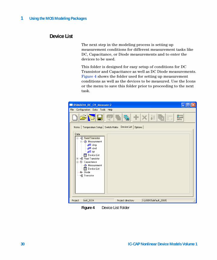
The next step in the modeling process is setting up measurement conditions for different measurement tasks like DC, Capacitance, or Diode measurements and to enter the devices to be used.
This folder is designed for easy setup of conditions for DC Transistor and Capacitance as well as DC Diode measurements. Figure 4 shows the folder used for setting up measurement conditions as well as the devices to be measured. Use the Icons or the menu to save this folder prior to proceeding to the next task.
Figure 4 Device List Folder
IC-CAP Nonlinear Device Models Volume 1

Using the MOS Modeling Packages 1
IC-CAP Nonlinear Device Models Vo
The left side of this folder shows a tree view of the data for this measurement project. This tree definition may be different for different models. The previous figure shows the tree used for extracting SOI device parameters.
The folder shows entries not normally present on BISM3/4 or PSP measurement projects. For example, there are no floating transistors to be measured in BSIM3 or 4 modeling tasks.
To expand the Transistor, Diode, and Capacitance entries, click the + sign to reveal a Measurement and Device List.
By clicking on Measurement, the right side of the folder shows predefined measurement sets as well as setups already selected for the specific measurement. To add a setup, click the icon.
You will be prompted to select a setup and enter a name for it. The new setup will be included in the tree below Measurement.
If you select one of the measurement setups inside the tree, the folder changes to reflect the measurement conditions valid for the selected setup.
lume 1 31
1 Using the MOS Modeling Packages
32
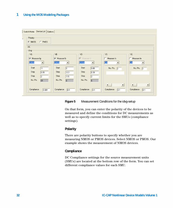
Figure 5 Measurement Conditions for the idvg-setup
On that form, you can enter the polarity of the devices to be measured and define the conditions for DC measurements as well as to specify current limits for the SMUs (compliance settings).
Polarity
There are polarity buttons to specify whether you are measuring NMOS or PMOS devices. Select NMOS or PMOS. Our example shows the measurement of NMOS devices.
Compliance
DC Compliance settings for the source measurement units (SMUs) are located at the bottom row of the form. You can set different compliance values for each SMU.
IC-CAP Nonlinear Device Models Volume 1
Using the MOS Modeling Packages 1
IC-CAP Nonlinear Device Models Vo
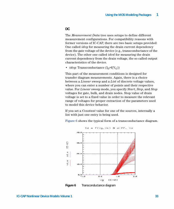
DC
The Measurement Data tree uses setups to define different measurement configurations. For compatibility reasons with former versions of IC-CAP, there are two basic setups provided: One called idvg for measuring the drain current dependency from the gate voltage of the device (e.g., transconductance of the device). The other one called idvd for measuring the drain current dependency from the drain voltage, the so called output characteristics of the device.
• idvg: Transconductance (ID=f(VG))
This part of the measurement conditions is designed for transfer diagram measurements. Again, there is a choice between a Linear sweep and a List of discrete voltage values, where you can enter a number of points and their respective value. For Linear sweep mode, you specify Start, Step, and Stop voltages for gate, bulk, and drain nodes. Stop value of drain voltage is set to a fixed value in order to measure the relevant range of voltages for proper extraction of the parameters used to model this device behavior.
If you set a Constant value for one of the sources, internally a list with just one entry is being used.
Figure 6 shows the typical form of a transconductance diagram.
Figure 6 Transconductance diagram
lume 1 33
34
1 Using the MOS Modeling Packages
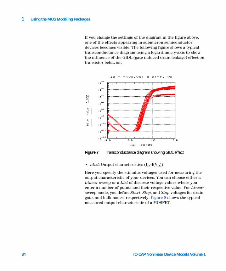
If you change the settings of the diagram in the figure above, one of the effects appearing in submicron semiconductor devices becomes visible. The following figure shows a typical transconductance diagram using a logarithmic y-axis to show the influence of the GIDL (gate induced drain leakage) effect on transistor behavior.
• idvd: Output characteristics (ID=f(VD))
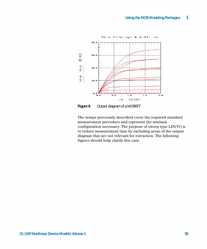
Here you specify the stimulus voltages used for measuring the output characteristic of your devices. You can choose either a Linear sweep or a List of discrete voltage values where you enter a number of points and their respective value. For Linear sweep mode, you define Start, Step, and Stop voltages for drain, gate, and bulk nodes, respectively. Figure 8 shows the typical measured output characteristic of a MOSFET.
Figure 7 Transconductance diagram showing GIDL effect
IC-CAP Nonlinear Device Models Volume 1
Using the MOS Modeling Packages 1
IC-CAP Nonlinear Device Models Vo
The setups previously described cover the required standard measurement procedure and represent the minimal configuration necessary. The purpose of sweep type LIN(Vt) is to reduce measurement time by excluding areas of the output diagram that are not relevant for extraction. The following figures should help clarify this case.
Figure 8 Output diagram of a MOSFET
lume 1 35

1 Using the MOS Modeling Packages
36
Figure 9 Output characteristic of the same device measured at differ-ent values of bulk voltage: left: vb = 0, right: vb = -1.2V
The gate voltage vg in the diagrams shown above has a fixed sweep from 0.6 to 1.8V. Because the bulk voltage changed, the threshold voltage changes, which in turn changes the output characteristic too. The curves marked with a red arrow are measurements at low current levels and therefore need a considerable amount of time due to the integration of noisy currents. Therefore, the lowest gate voltage consumes a lot of time with minimal benefit for the extraction. For example, it would be better to start the left hand diagram at vg = 0.7V and the right hand diagram at vg = 0.8V. This can be achieved by making the gate voltage sweep starting points dependent on Vth of this device.
IC-CAP Nonlinear Device Models Volume 1
Using the MOS Modeling Packages 1
IC-CAP Nonlinear Device Models Vo
The LIN f(Vth)-sweep is a linear sweep using a starting value dependent on an extracted threshold voltage value from another Vg-type sweep.
This sweep needs a reference to another sweep of type vg. The stop condition is fixed and the start point is depending on the threshold voltage of the reference sweep. If this sweep is selected, the setup must not have any other sweeps (e.g., vb, vs, ...) because the IC-CAP rectangular data format does not support it. The referenced sweep must include the vb, vs, (ve) value of the actual sweep, which is defined to be a constant value. In the case of vd (1st sweep), the threshold voltages in the reference sweep at all vd values are taken and a mean value is generated.
Furthermore, it is necessary to specify a resolution value in order to send reasonable voltage values to a measuring instrument. Taking this into account, the effective start and step values are calculated according to the following formulas:
The following table shows the minimum source configuration. It is now possible to select an output from each source, for example, ig, ib, id, is. The source’s output current is in bold letters to indicate that it was used as the minimum required output.
Vstep raw,Vstop Vth– Voffset–
No.Pts -1------------------------------------------------=
Vstep Vresolution floor⋅Vstep raw, Vresolution+
Vresolution--------------------------------------------------------
=
Vstart Vstop No.Pts -1( )– Vstep⋅=
lume 1 37
38
1 Using the MOS Modeling Packages
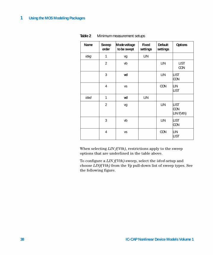
When selecting LIN f(Vth), restrictions apply to the sweep options that are underlined in the table above.
To configure a LIN f(Vth)-sweep, select the idvd-setup and choose LINf(Vth) from the Vg pull-down list of sweep types. See the following figure.
Table 2 Minimum measurement setups
Name Sweep order
Mode voltage to be swept
Fixed settings
Default settings
Options
idvg 1 vg LIN
2 vb LIN LISTCON
3 vd LIN LISTCON
4 vs CON LINLIST
idvd 1 vd LIN
2 vg LIN LISTCONLIN f(Vth)
3 vb LIN LISTCON
4 vs CON LINLIST
IC-CAP Nonlinear Device Models Volume 1
Using the MOS Modeling Packages 1
IC-CAP Nonlinear Device Models Vo
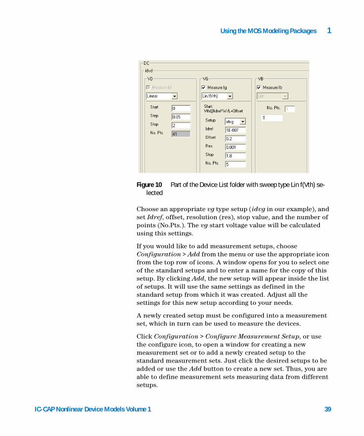
Figure 10 Part of the Device List folder with sweep type Lin f(Vth) se-lected
Choose an appropriate vg type setup (idvg in our example), and set Idref, offset, resolution (res), stop value, and the number of points (No.Pts.). The vg start voltage value will be calculated using this settings.
If you would like to add measurement setups, choose Configuration > Add from the menu or use the appropriate icon from the top row of icons. A window opens for you to select one of the standard setups and to enter a name for the copy of this setup. By clicking Add, the new setup will appear inside the list of setups. It will use the same settings as defined in the standard setup from which it was created. Adjust all the settings for this new setup according to your needs.
A newly created setup must be configured into a measurement set, which in turn can be used to measure the devices.
Click Configuration > Configure Measurement Setup, or use the configure icon, to open a window for creating a new measurement set or to add a newly created setup to the standard measurement sets. Just click the desired setups to be added or use the Add button to create a new set. Thus, you are able to define measurement sets measuring data from different setups.
lume 1 39

40
1 Using the MOS Modeling Packages
Transistor Device List
Select Device List from the tree to enter the devices to be measured. When creating a new project, the device list contains predefined device names that you can simply overwrite with device names of your choice.
The device list table contains additional columns for each temperature you’ve entered on the Temperature Setup folder.
Figure 11 Device List tree with entries for the devices to be measured
The column named Measure shows the allocation of measurement sets to the devices. For each device, you have to select a measurement set to be used for this device. Using the Device List, you can define which set will be used for which device. Select Configuration > Configure Measurement Set to display a list of devices to be measured. Select a device, then select one of the available measurement sets you wish to assign to this device and click OK.
NOTE Selecting Configuration > Configure Measurement Set from the menu actually has two different meanings, depending on the subfolder selected from the tree. If the Measurement subfolder is selected, Configure Measurement Set means to add a new measurement set to the list of available sets. If the Device List subfolder is selected, then you can define which set to use for which device.
IC-CAP Nonlinear Device Models Volume 1
Using the MOS Modeling Packages 1
IC-CAP Nonlinear Device Models Vo
The Device List under the Transistor branch in the tree view is used to enter DUT names, geometries, and connections to the appropriate DUTs. Since there are differences between the BSIM3 and BSIM4/PSP models, some parameters are to be used only inside the appropriate model and only activated there. The BSIM4/PSP models enables stress effect modeling, which is not possible in BSIM3. Therefore, all stress effect parameters are only used inside the BSIM4/PSP Modeling Packages and are activated only there.
The Configuration menu enables you to set BSIM4/PSP-specific values. You can use different area and perimeter values as well as Number of Squares for the Drain and Source regions of the transistors to be measured (AS, AD, PS, PD, NRD, NRS). Further on you can set stress effect parameters SA, SB, SD. See “Stress Effect Modeling” on page 270 for details.
If you deactivate one of the Configuration menu points (AS=AD, PS=PD, for example), additional columns appear in the Device List table.
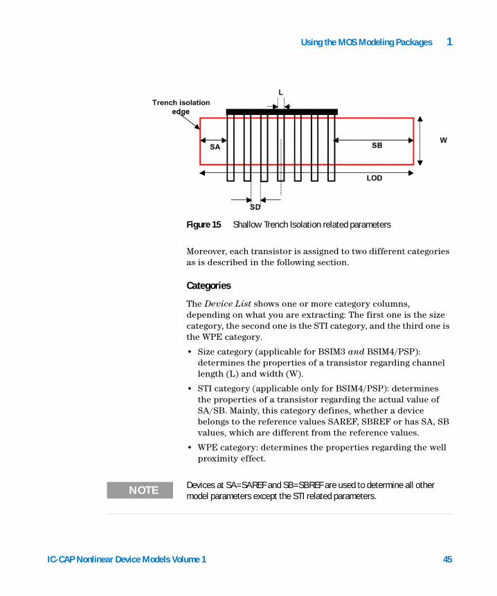
Now you can enter STI-related parameters. Refer to Figure 15 for details on these parameters.
Well Proximity Effect
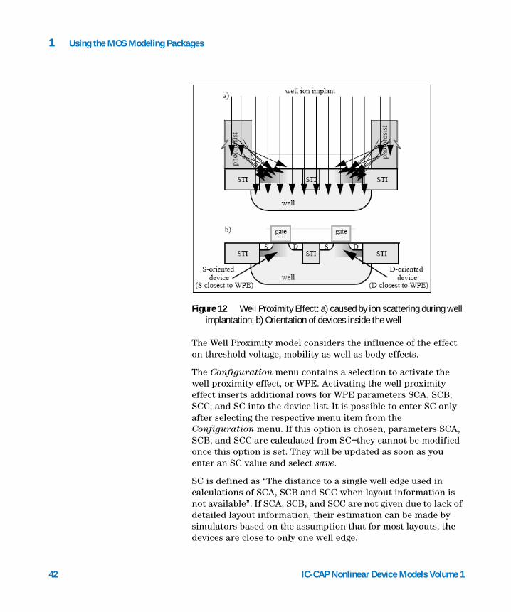
Taken from: P. G. Drennan, M. L. Kniffin, D. R. Locascio “Implications of Proximity Effects for Analog Design”; to be found at http://www.ieee-cicc.org/06-8-6.pdf
Highly scaled bulk CMOS technologies make use of high energy implants to form the deep retrograde well profiles needed for latch-up protection and suppression of lateral punch-through. During the implant process, atoms can scatter laterally from the edge of the photoresist mask and become embedded in the silicon surface in the vicinity of the well edge, as illustrated in Figure 12. The result is a well surface concentration that changes with lateral distance from the mask edge, over the range of 1um or more. This lateral non-uniformity in well doping causes the MOSFET threshold voltages and other electrical characteristics to vary with the distance of the transistor to the edge of the well. This phenomenon is commonly known as the well proximity effect (WPE).
lume 1 41
42
1 Using the MOS Modeling Packages
Figure 12 Well Proximity Effect: a) caused by ion scattering during wellimplantation; b) Orientation of devices inside the well
The Well Proximity model considers the influence of the effect on threshold voltage, mobility as well as body effects.
The Configuration menu contains a selection to activate the well proximity effect, or WPE. Activating the well proximity effect inserts additional rows for WPE parameters SCA, SCB, SCC, and SC into the device list. It is possible to enter SC only after selecting the respective menu item from the Configuration menu. If this option is chosen, parameters SCA, SCB, and SCC are calculated from SC−they cannot be modified once this option is set. They will be updated as soon as you enter an SC value and select save.
SC is defined as “The distance to a single well edge used in calculations of SCA, SCB and SCC when layout information is not available”. If SCA, SCB, and SCC are not given due to lack of detailed layout information, their estimation can be made by simulators based on the assumption that for most layouts, the devices are close to only one well edge.
IC-CAP Nonlinear Device Models Volume 1
Using the MOS Modeling Packages 1
IC-CAP Nonlinear Device Models Vo
For details, see the BSIM4 manual from the University of Berkeley. Their website contains a link where you can download the complete manual. The address is http://www-device.eecs.berkeley.edu/~bsim3/bsim4_get.html
Defining Devices
For your convenience, there are predefined DUTs on the Device List folder when creating a new project. You can either use those predefined DUTs, only adjusting names, device geometries, connections and so on, or you can delete existing DUTs and add your own.
• Choose Add from the row of icons or Configuration > Add from the menu. You will be prompted for the DUTs to copy. Select the desired names and choose Add from the Add DUT window. It is also possible to set the number of copies of the selected DUTs. Added DUTs will automatically get the extension “_new” to the name of the original DUTs.
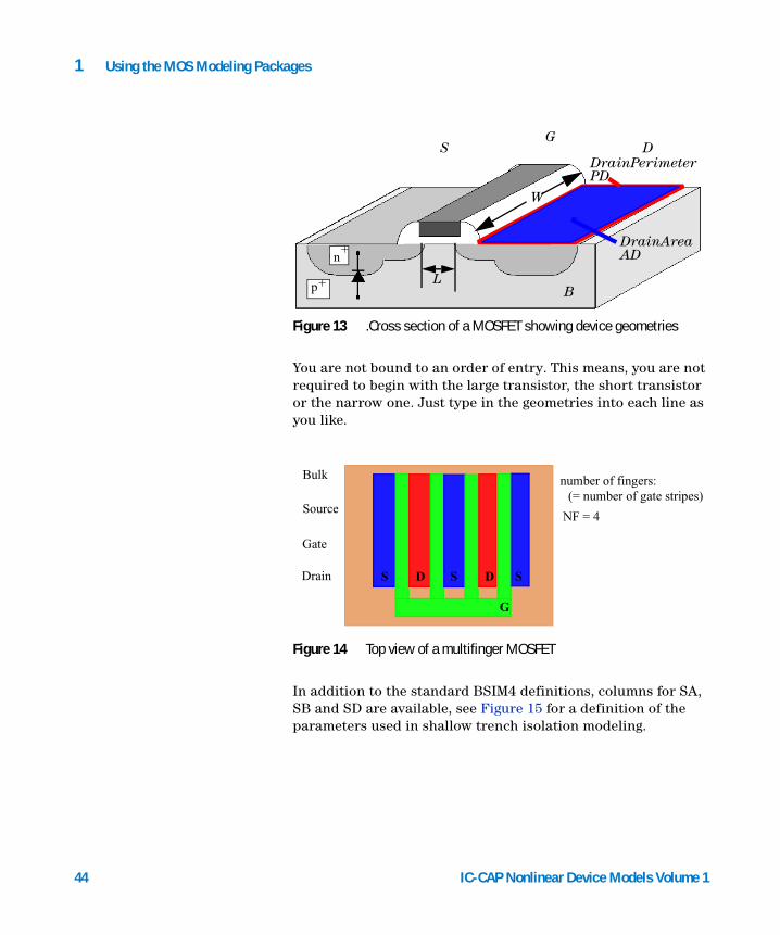
For each line, enter a name for the DUT, gate length and width (L, W), drain and source areas (AD, AS), perimeter length of drain and source (PD, PS), and the number of device fingers (NF) of the transistor to be measured. If modeling stress effects in BSIM4 or PSP, enter SA, SB, and SD as well. See Figure 13 as well as Figure 14 for details on device geometry, respective Figure 15 for details on STI modeling parameters. Well Proximity modeling requires the entry of parameters SCA, SCB, SCC, and/or SC.
NOTE Remember, all geometries are to be given in microns (µm).
Geometries
Shown in the following two figures are views of MOSFET’s, where you can find the geometries required by the BSIM3 and BSIM4/PSP Modeling Packages.
lume 1 43
44
1 Using the MOS Modeling Packages
You are not bound to an order of entry. This means, you are not required to begin with the large transistor, the short transistor or the narrow one. Just type in the geometries into each line as you like.
In addition to the standard BSIM4 definitions, columns for SA, SB and SD are available, see Figure 15 for a definition of the parameters used in shallow trench isolation modeling.
Figure 13 .Cross section of a MOSFET showing device geometries
Figure 14 Top view of a multifinger MOSFET
W
DG
SDrainPerimeterPD
DrainAreaAD
LBp+
n+
Bulk
Source
Drain
number of fingers:
G
DD SS S
(= number of gate stripes)
NF = 4
Gate
IC-CAP Nonlinear Device Models Volume 1
Using the MOS Modeling Packages 1
IC-CAP Nonlinear Device Models Vo
Moreover, each transistor is assigned to two different categories as is described in the following section.
Categories
The Device List shows one or more category columns, depending on what you are extracting: The first one is the size category, the second one is the STI category, and the third one is the WPE category.
• Size category (applicable for BSIM3 and BSIM4/PSP): determines the properties of a transistor regarding channel length (L) and width (W).
• STI category (applicable only for BSIM4/PSP): determines the properties of a transistor regarding the actual value of SA/SB. Mainly, this category defines, whether a device belongs to the reference values SAREF, SBREF or has SA, SB values, which are different from the reference values.
• WPE category: determines the properties regarding the well proximity effect.
Figure 15 Shallow Trench Isolation related parameters
NOTE Devices at SA=SAREF and SB=SBREF are used to determine all other model parameters except the STI related parameters.
lume 1 45

46
1 Using the MOS Modeling Packages
The Configuration menu enables you to Sort the entries into an order or to Set the size category of your devices manually. See “Transistors for DC measurements” on page 422.
You can use Configuration > Sort or the appropriate icon to set the size category of your devices automatically. Otherwise, you are required to enter the size category manually using the form shown in Figure 16.
The device category is used for extraction purposes. See “Transistors for DC measurements” on page 422 in the BSIM3 Characterization chapter for an explanation of categories and requirements for proper extraction of device parameters as well as the paragraph about “Stress Effect Modeling” on page 270 inside Chapter 4, “BSIM4 Characterization”.
If you would like to delete devices:
Figure 16 Set size category
IC-CAP Nonlinear Device Models Volume 1
Using the MOS Modeling Packages 1
IC-CAP Nonlinear Device Models Vo
• Choose Delete from the row of icons or from the Configuration > Delete menu. You will be prompted with a list of DUTs. Select the DUTs to be deleted and choose Delete on the Delete DUT form. A prompt dialog box appears. Select OK if you are satisfied with your choice of DUTs to be deleted.
According to your choice of temperatures on the Temperature Setup folder, one or more columns marked with the temperatures you have entered appear. The fields of those columns show either (0) for no measured data available, (M) for DUT already measured or (-) for DUT not to be measured at that temperature.
• To select devices to be measured at different temperatures: Choose Temperature Measurement from the icons or from the Configuration menu. You will be prompted with a list of DUTs. Select the devices to be measured at those temperatures entered in the Temperature Setup folder and click OK. You can select more than one DUT at a time for temperature measurement by repeated clicks on each one you want to choose.
NOTE You cannot prevent a DUT from being measured at TNOM. All DUTs are measured at that temperature. If you have entered one or more temperatures (T1 and T2, for example) on the Temperature Setup folder, the DUTs selected for temperature measurement are all measured at those temperatures. In other words, you cannot select a DUT for measurement at temperature T1 but not at temperature T2.
NOTE To extract temperature effects on parameters, a large, a short, and a small device is necessary!
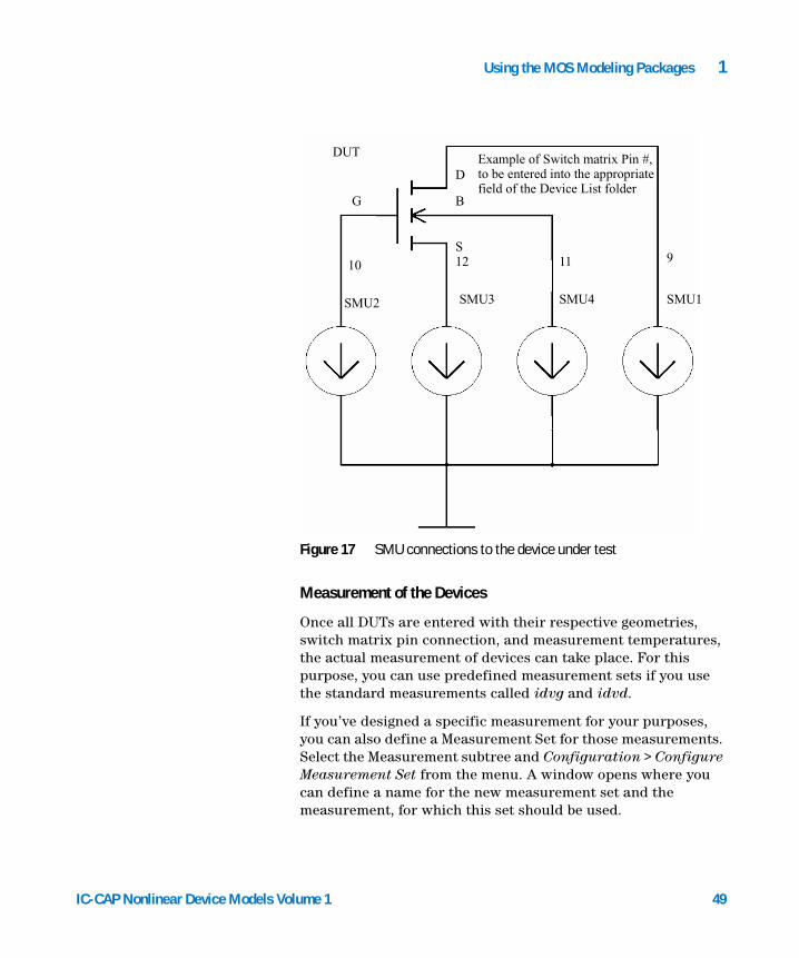
You can enter a comment for each DUT. If you are using a switch matrix, you can enter a module name and the pin numbers of the switch matrix pin connections to the transistor in the fields below the node names (those fields are present only if the use of a switch matrix is selected on the Switch Matrix folder). See Figure 17 for details.
lume 1 47

1 Using the MOS Modeling Packages
NOTE For the Agilent E5250, the port number to be entered consists of 3 numbers.
If, for example, SMU1 is to be connected to Card No.1, Port No. 3: Enter the number 103 into the field below the transistor’s node name. Port No. 12 for Card No. 4 would have to be entered as 412.
NOTE When using module names to measure devices with probe cards, pay attention to the node numbers you are entering. Each device uses 4 connections to the switch matrix. You have to enter the correct pin numbers for each DUT and must not exceed the total pin count for each port of your matrix.
48
Connections to the DUTs
The following figure shows an example for a connected device under test (DUT) to the source measurement units (SMUs) during DC Transistor measurements. The node numbers shown are to be entered into the fields on the Device List folder, see Figure 11 on page 40. The above mentioned figure shows “0” under all terminal names. Those numbers have to be changed to “10” for the gate, “12” for the source, “11” for the bulk, and “9” for the drain terminal to reflect the connections used inside the following schematic. Please be careful to use the names SMU1...SMU4 during hardware setup in IC-CAP, since these are required by the measurement module of the BSIM3/4 and PSP Modeling Packages.
IC-CAP Nonlinear Device Models Volume 1
Using the MOS Modeling Packages 1
IC-CAP Nonlinear Device Models Vo
Measurement of the Devices
Once all DUTs are entered with their respective geometries, switch matrix pin connection, and measurement temperatures, the actual measurement of devices can take place. For this purpose, you can use predefined measurement sets if you use the standard measurements called idvg and idvd.
If you’ve designed a specific measurement for your purposes, you can also define a Measurement Set for those measurements. Select the Measurement subtree and Configuration > Configure Measurement Set from the menu. A window opens where you can define a name for the new measurement set and the measurement, for which this set should be used.
Figure 17 SMU connections to the device under test
DUT
D
B
S
G
SMU2 SMU3 SMU4 SMU1
10 12 11 9
Example of Switch matrix Pin #,to be entered into the appropriate field of the Device List folder
lume 1 49
50
1 Using the MOS Modeling Packages
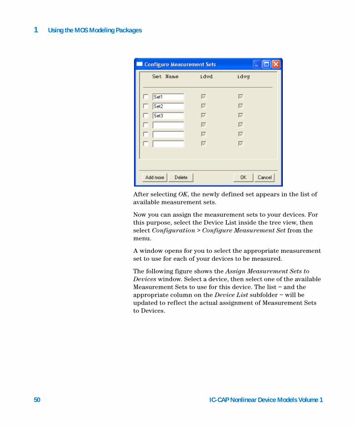
After selecting OK, the newly defined set appears in the list of available measurement sets.
Now you can assign the measurement sets to your devices. For this purpose, select the Device List inside the tree view, then select Configuration > Configure Measurement Set from the menu.
A window opens for you to select the appropriate measurement set to use for each of your devices to be measured.
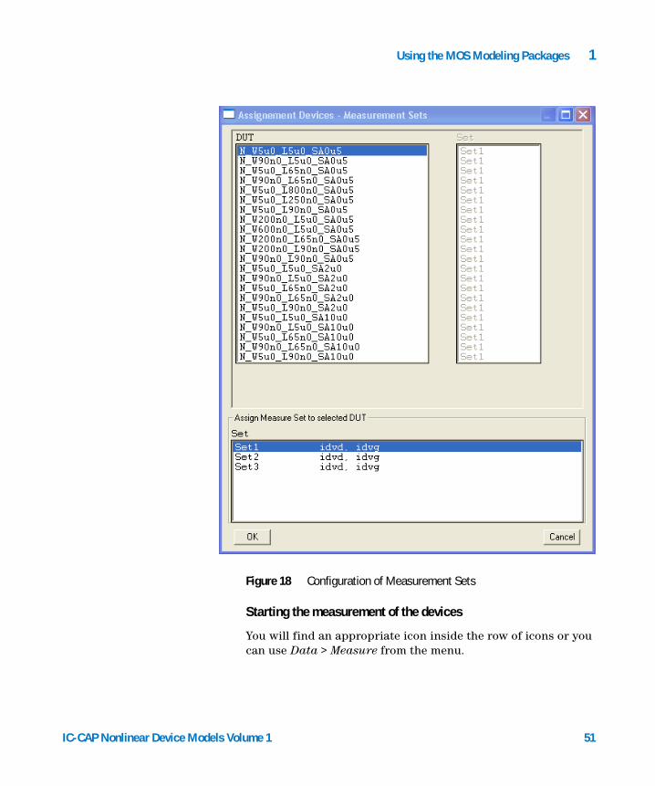
The following figure shows the Assign Measurement Sets to Devices window. Select a device, then select one of the available Measurement Sets to use for this device. The list − and the appropriate column on the Device List subfolder − will be updated to reflect the actual assignment of Measurement Sets to Devices.
IC-CAP Nonlinear Device Models Volume 1
Using the MOS Modeling Packages 1
IC-CAP Nonlinear Device Models Vo
Figure 18 Configuration of Measurement Sets
Starting the measurement of the devices
You will find an appropriate icon inside the row of icons or you can use Data > Measure from the menu.
lume 1 51
52
1 Using the MOS Modeling Packages
• To start measurement of the devices: Click the Measure icon (or Data > Measure) from the menu and select the DUT
or Module to be measured using the dialog box that opens. You can select a measurement temperature (if there is a temperature other than TNOM defined in the temperature setup folder) as well as a specific DUT or a Module (containing all DUTs to be measured at a specific temperature). If you select a temperature other than TNOM, (must be defined under TemperatureSetup), only the devices set up for measurement at that temperature are selectable for measurement. Start measurement with Measure (or MeasureDUT in BSIM4/PSP) on that dialog box. If measuring at elevated temperatures, be sure to wait until your devices are heated up or cooled down to the desired temperature.
NOTE For your convenience, you will find a supplemental model file called “prober_control.mdl” which is suitable to be used with automatic temperature measurements under the directories $ICCAP_ROOT/ examples/modelFiles/mosfet/BSIM3(4)/examples/waferprober. Tailor this model file to your specific Thermochuck model and requirements. Otherwise, be sure to set chuck temperature manually!
IC-CAP does not support heated chuck drivers.
If you select measurement of a module, all DUTs in this module are measured automatically if the use of a switch matrix is activated.
The DUTs/Setup folder in the BSIM3/4_DC_CV_Measure model contains an AutoMeasure setup for the Configuration DUT. Using this AutoMeasure setup, you can program automatic measurements for all DUTs in one module.
NOTE Automatic measurement uses a macro for the wafer prober. This macro is programmed to start measurement as soon as the wafer prober has reached its programmed destination.
IC-CAP Nonlinear Device Models Volume 1

Using the MOS Modeling Packages 1
IC-CAP Nonlinear Device Models Vo
You’ll find the macro “Example_Wafer_Prober” and it’s transforms together with a description of the transforms in the Macro folder of the BSIM3/4_DC_CV_Measure model.
• If you would like to clear some or all measured data, select Clear Data from the Data menu. You can select whether you would like to clear measured data of some or all DUTs at specified temperatures and choose Clear Data to delete measured data files.
• Using the Data menu’s Synthesize Measured Data, you can simulate data from existing model parameters. By selecting this feature, already measured data files are overwritten with synthesized data. You will be prompted before existing data files are overwritten.
There is the choice of either synthesizing data or loading an MPS File.
This synthesized data uses the voltages set on the Measurement Conditions folder to generate “measurement” data from a known set of SPICE parameters. This feature might be especially useful to convert parameters of other models into BSIM4 parameters by loading the created “measurement data” into the extraction routines and extract BSIM4 parameters.
• To see the diagrams of what has just been measured, use the Display Plots icon or Data > Display Plots. You will see a Multiplot window with different folders. Using those folders, you can change the plot types as well as the devices, whose plots are to be shown. This is a convenient way to detect measurement errors before starting the extraction routines.
• If you are satisfied with the data plots you’ve just measured, choose the Close Plots icon to close the displayed plots of measured data.
• The Data menu has an entry Check Data consistency to see if measurement errors have occurred. If you select this menu item, a Multiplot window opens for a quick consistency check. If errors are detected, an error window opens and gives you a hint on what might be inconsistent within your measurements.
lume 1 53
54
1 Using the MOS Modeling Packages
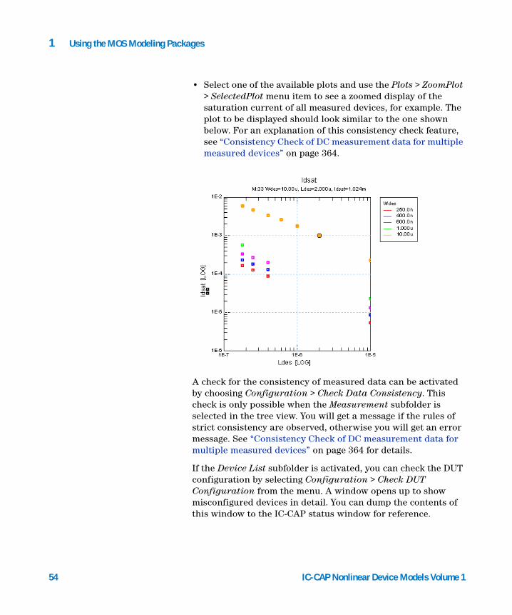
• Select one of the available plots and use the Plots > ZoomPlot > SelectedPlot menu item to see a zoomed display of the saturation current of all measured devices, for example. The plot to be displayed should look similar to the one shown below. For an explanation of this consistency check feature, see “Consistency Check of DC measurement data for multiple measured devices” on page 364.
A check for the consistency of measured data can be activated by choosing Configuration > Check Data Consistency. This check is only possible when the Measurement subfolder is selected in the tree view. You will get a message if the rules of strict consistency are observed, otherwise you will get an error message. See “Consistency Check of DC measurement data for multiple measured devices” on page 364 for details.
If the Device List subfolder is activated, you can check the DUT configuration by selecting Configuration > Check DUT Configuration from the menu. A window opens up to show misconfigured devices in detail. You can dump the contents of this window to the IC-CAP status window for reference.
IC-CAP Nonlinear Device Models Volume 1
Using the MOS Modeling Packages 1
IC-CAP Nonlinear Device Models Vo
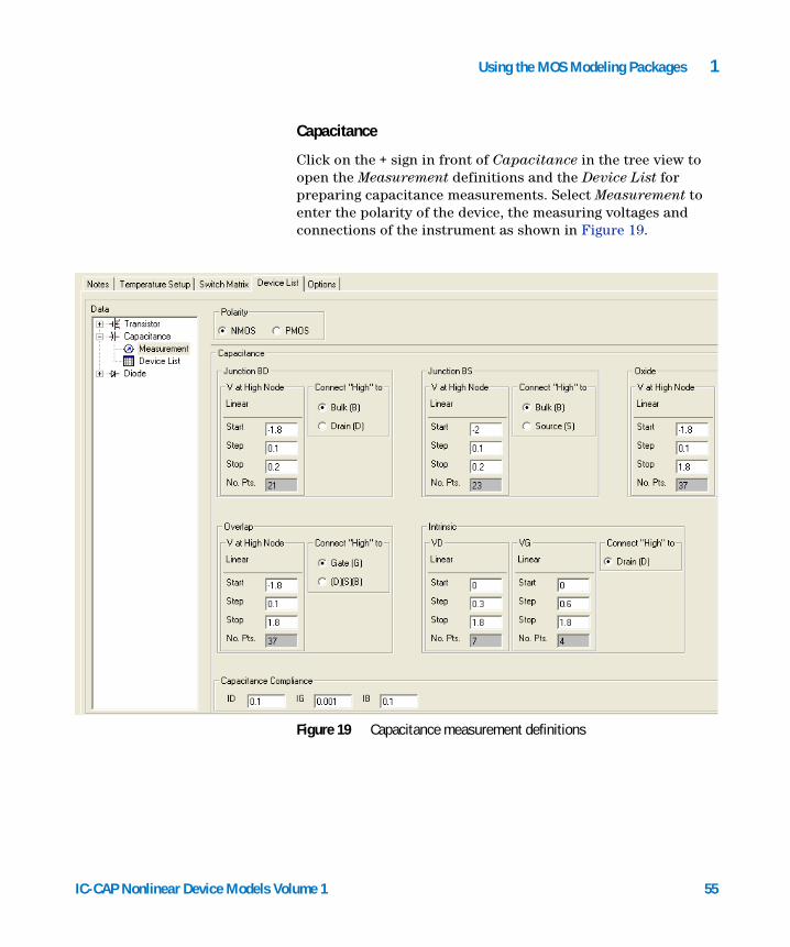
Capacitance
Click on the + sign in front of Capacitance in the tree view to open the Measurement definitions and the Device List for preparing capacitance measurements. Select Measurement to enter the polarity of the device, the measuring voltages and connections of the instrument as shown in Figure 19.
Figure 19 Capacitance measurement definitions
lume 1 55

56
1 Using the MOS Modeling Packages
Physically Connecting Test Structures to your Capacitance Measurement Device
The following figure shows how to connect the CV instrument to measure oxide and overlap capacitances. See also the paragraph on test structures for CV measurement. In Table 67 on page 426 you’ll find recommended test structures for specific capacitances to be measured together with recommended instrument connections.
The following figure shows a typical gate-to-drain/source overlap capacitance diagram that you would expect to measure with this type of connection and the default values for Start, Step, and Stop voltage VG.
Figure 20 Measurement of oxide and overlap capacitance
NOTE To correctly extract overlap capacitance effects, two devices are essential: Standard CV measurement masks the channel capacity in short channel devices. This is the so called Short Channel Effect.
To overcome this masking, you need a short channel device for proper extraction of overlap capacitance parameters. To extract the parameter NGATE, you need to measure a long channel device in inversion since there is no short channel effect present in such a device.
IC-CAP Nonlinear Device Models Volume 1

Using the MOS Modeling Packages 1
IC-CAP Nonlinear Device Models Vo
Test Structures for CV Measurements
See Table 67 on page 426 for a table of recommended test structures for CV measurements.
Capacitance Device List
Click on Device List to define the devices to be measured and their respective geometries. See the following cut out for an example.
Figure 21 Example diagram of measured overlap capacity
min(C g_sdb)
lume 1
57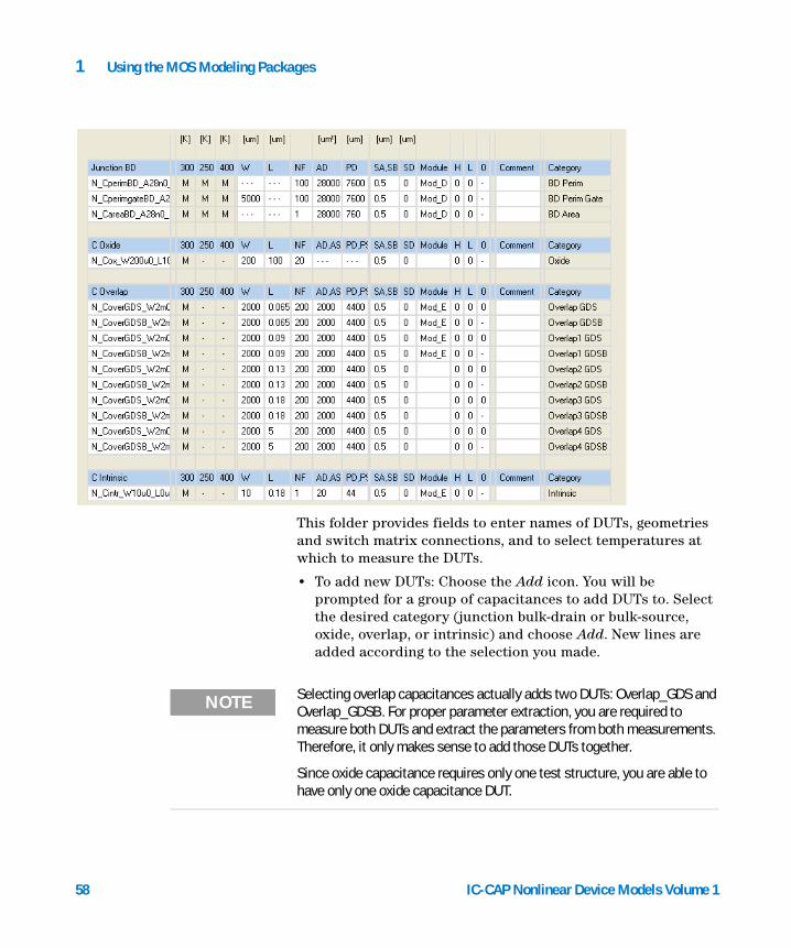
58
1 Using the MOS Modeling Packages
This folder provides fields to enter names of DUTs, geometries and switch matrix connections, and to select temperatures at which to measure the DUTs.
• To add new DUTs: Choose the Add icon. You will be prompted for a group of capacitances to add DUTs to. Select the desired category (junction bulk-drain or bulk-source, oxide, overlap, or intrinsic) and choose Add. New lines are added according to the selection you made.
NOTE Selecting overlap capacitances actually adds two DUTs: Overlap_GDS and Overlap_GDSB. For proper parameter extraction, you are required to measure both DUTs and extract the parameters from both measurements. Therefore, it only makes sense to add those DUTs together.
Since oxide capacitance requires only one test structure, you are able to have only one oxide capacitance DUT.
IC-CAP Nonlinear Device Models Volume 1
Using the MOS Modeling Packages 1
IC-CAP Nonlinear Device Models Vo
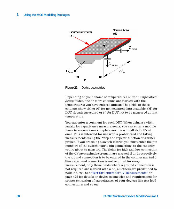
For each line, you can change the predefined name for the DUT and enter necessary geometrical data. For your convenience, only relevant data should be entered for a specific group of capacities. Relevant data fields are shown with white background and can be edited. Gray shaded data fields are not editable. For example, DUTs to measure bulk-drain junction capacitances do not require gate length and width (L, W), source area (AS) and perimeter length of source (PS) geometrical data. You only have to provide drain area (AD) and drain perimeter (PD) as well as the number of device fingers (NF) of the transistor to be measured. See Figure 22 for some details on capacitances and geometries.
NOTE W, AD, AS, PD, and PS are total values including all fingers of the device!
NOTE Usually, you use single finger transistors for DC measurements. Multifinger devices are common only in high frequency characterization of MOS devices, since the input resistance of a network analyzer is typically 50 Ohm.
Remember, all geometries are to be given in microns (µm).
lume 1 59
60
1 Using the MOS Modeling Packages
Depending on your choice of temperatures on the Temperature Setup folder, one or more columns are marked with the temperatures you have entered appear. The fields of those columns show either (0) for no measured data available, (M) for DUT already measured or (-) for DUT not to be measured at that temperature.
You can enter a comment for each DUT. When using a switch matrix for capacitance measurements, you can enter a module name to measure one complete module with all its DUTs at once. This is intended for use with a prober card and taking measurements using the “step and repeat” function of a wafer prober. If you are using a switch matrix, you must enter the pin numbers of the switch matrix pin connections to the capacity you‘re about to measure. The fields for high and low connection of the CV measuring instrument are marked H or L respectively, the ground connection is to be entered in the column marked 0. Since a ground connection is not required for every measurement, only those fields where a ground connection is not required are marked with a ”-”, all others are predefined to node No. “0”. See “Test Structures for CV Measurements” on page 425 for details on device geometries and requirements for proper extraction of capacitances of your devices like test lead connections and so on.
Figure 22 Device geometries
Source PerimeterPS
Source AreaAS
IC-CAP Nonlinear Device Models Volume 1
Using the MOS Modeling Packages 1
IC-CAP Nonlinear Device Models Vo
• To delete DUTs: Choose the Delete icon or Delete from the Configure menu. You will be prompted with a list of DUTs. Select the DUTs to be deleted and choose Delete on the Delete DUT folder. A prompt dialog box appears. Select OK if you are satisfied with your choice of DUTs to be deleted.
• To select devices to be measured at different temperatures: Choose the Temperature Measurement icon or Temperature Measurement from the Configuration menu. You will be prompted with a list of DUTs. Select the devices to be measured at those temperatures entered in the Temperature Setup folder and click OK.
NOTE You cannot prevent a DUT from being measured at TNOM. All DUTs are measured automatically at that temperature. If you have entered one or more temperatures on the Temperature Setup folder, the DUTs selected for temperature measurement are all measured at those temperatures. In other words, you cannot select a DUT for measurement at temperature T1 but not at another temperature T2.
• To start measurement of the devices: Choose the Measure icon and select the DUTs to be measured on the dialog box that opens. You can select measurement temperature (if there is a temperature other than TNOM defined in the Temperature Setup folder) as well as a specific DUT or all DUTs. Start the measurement with Measure on that dialog box. If measuring at elevated temperatures, be sure to wait until your devices are heated up or cooled down to the desired temperature.
• If you would like to clear some or all measured data, choose Clear Data from the Data menu. You can select whether you would like to clear measured data of some or all DUTs at specified temperatures and click Clear Data to delete measured data files.
lume 1 61

62
1 Using the MOS Modeling Packages
• Using Synthesize Measured Data from the Data menu, you can simulate capacitance data from existing parameters. These synthesized data use the voltages set on the Measurement Conditions folder to generate “measurement” data from a known set of SPICE parameters. It might be especially useful to convert parameters of other models into BSIM3 or BSIM4 parameters by loading the created “measurement data” into the extraction routines and extract parameters for the desired model.
• To see the diagrams of what has just been measured, click the Display Plots icon. You will see a dialog box to select which measured data set you would like to display. After choosing the plots you would like to see, click Display Plots on that dialog box to open the selected plots. This is a convenient way to detect measurement errors before starting the extraction routines.
• If you are satisfied with the data you have just measured, choose Close Plots to close the windows that show diagrams of measured data.
Diode
This part of the Data tree is used to define measurements for Junctions/Diodes of the devices to be measured. First, define the measurement conditions to reflect the desired voltages, Number of Points, and Compliances used for the measurement.
IC-CAP Nonlinear Device Models Volume 1
Using the MOS Modeling Packages 1
IC-CAP Nonlinear Device Models Vo
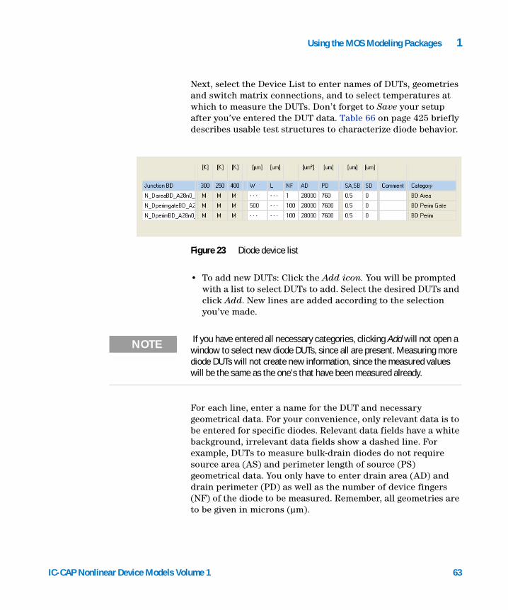
Next, select the Device List to enter names of DUTs, geometries and switch matrix connections, and to select temperatures at which to measure the DUTs. Don’t forget to Save your setup after you’ve entered the DUT data. Table 66 on page 425 briefly describes usable test structures to characterize diode behavior.
• To add new DUTs: Click the Add icon. You will be prompted with a list to select DUTs to add. Select the desired DUTs and click Add. New lines are added according to the selection you’ve made.
Figure 23 Diode device list
NOTE If you have entered all necessary categories, clicking Add will not open a window to select new diode DUTs, since all are present. Measuring more diode DUTs will not create new information, since the measured values will be the same as the one’s that have been measured already.
For each line, enter a name for the DUT and necessary geometrical data. For your convenience, only relevant data is to be entered for specific diodes. Relevant data fields have a white background, irrelevant data fields show a dashed line. For example, DUTs to measure bulk-drain diodes do not require source area (AS) and perimeter length of source (PS) geometrical data. You only have to enter drain area (AD) and drain perimeter (PD) as well as the number of device fingers (NF) of the diode to be measured. Remember, all geometries are to be given in microns (µm).
lume 1 63
1 Using the MOS Modeling Packages
NOTE W, AD, AS, PD, and PS are total values including all fingers of the device!
64
Depending on your choice of temperatures on the Temperature Setup folder, one or more columns marked with the temperatures you have entered appear. The fields of those columns show either (0) for no measured data available, (M) for DUT already measured or (-) for DUT not to be measured at that temperature.
• You can enter a comment for each DUT. If you are using a switch matrix, you can enter a module name as well as the pin numbers of the switch matrix pin connections to the transistor. Only relevant connections should be entered. In the case of the bulk-drain diode, no source connection should be entered (the appropriate field shows a dashed line). See Figure 22 on page 60 for details on device geometries and Table 68 on page 430 for requirements on a proper extraction of diode data.
• To delete DUTs: Choose Delete from the icons or menu. You will be prompted with a list of DUTs. Select the DUTs to be deleted and click Delete on the Delete DUT folder. A prompt dialog box appears. Choose OK if you are satisfied with your choice of DUTs to be deleted.
• To select devices to be measured at different temperatures: Choose Temperature Measurement from the Configuration menu. You will be prompted with a list of DUTs. Select the devices to be measured at the temperatures entered in the Temperature Setup folder and click OK.
NOTE You cannot prevent a DUT from being measured at TNOM. All DUTs are measured automatically at that temperature. If you have entered one or more temperatures on the Temperature Setup folder, the DUTs selected for temperature measurement are all measured at those temperatures. In other words, you cannot select a DUT for measurement at temperature T1 but not at another temperature T2.
IC-CAP Nonlinear Device Models Volume 1
Using the MOS Modeling Packages 1
IC-CAP Nonlinear Device Models Vo
• To start measurement of the devices: Click the Measure icon and select the DUTs to be measured on the dialog box that opens. You can select measurement temperature (if there is a temperature other than TNOM defined in the Temperature Setup folder) as well as a specific DUT. Start the measurement with Measure on that dialog box. If measuring at elevated temperatures, be sure to wait until your devices are heated or cooled down to the desired temperature.
• If you would like to clear data of some or all measured DUTs, use Clear Data from the Data menu. Select whether you would like to clear measured data of some or all DUTs at specified temperatures, and click Clear Data to delete measured data files.
• Using Synthesize Measured Data from the Data menu, you can simulate data from existing parameters. This synthesized data uses the voltages set on the Measurement Conditions folder to generate “measurement” data from a known set of SPICE parameters.
• To see the diagrams of what has just been measured, use the Display Plots icon. You will see a dialog box to select which measured data set you would like to display. Choosing the plots you would like to see, opens the selected plots. This is a convenient way to detect measurement errors before starting the extraction routines.
• If you are satisfied with the data you just measured, use the Close Plots icon to close the windows that show diagrams of measured data.
Drain/Source – Bulk Diodes for DC Measurements
For test structures to measure DC Drain/Source-to-Bulk diodes, see “Drain/Source – Bulk Diodes for DC Measurements” on page 425.
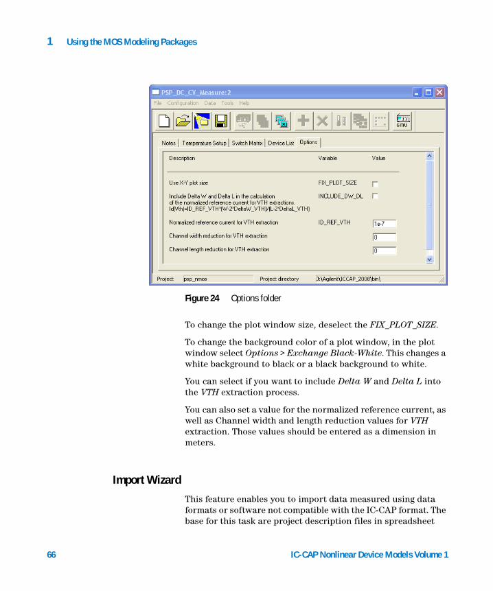
Options
This folder lets you define options for the appearance of the plot windows.
lume 1 65
66
1 Using the MOS Modeling Packages
To change the plot window size, deselect the FIX_PLOT_SIZE.
To change the background color of a plot window, in the plot window select Options > Exchange Black-White. This changes a white background to black or a black background to white.
You can select if you want to include Delta W and Delta L into the VTH extraction process.
You can also set a value for the normalized reference current, as well as Channel width and length reduction values for VTH extraction. Those values should be entered as a dimension in meters.
Figure 24 Options folder
Import Wizard
This feature enables you to import data measured using data formats or software not compatible with the IC-CAP format. The base for this task are project description files in spreadsheet
IC-CAP Nonlinear Device Models Volume 1

Using the MOS Modeling Packages 1
IC-CAP Nonlinear Device Models Vo
format (.csv files). As a template for these csv files, the File > Export menu contains selections to create devices lists for DC, Capacitance, and Diode data. Load a project into the IC-CAP Measurement module, then select either DC device list, Capacitance device list, or Diode device list. A csv style file will be created. This file can be opened with EXCEL, for example. It contains all device data that was entered into the DC, Capacitance, or Diode DUTs folder.
You can edit the project document or you can create a new one using the same format. The first row of the sheet contains keywords. The values below these keywords will be read into IC-CAP and are assigned to the appropriate values in the MOS Modeling Toolkits. By default, the list contains a certain set of keywords. However, you can add more keywords to help define the import paths. All keywords can be used later to describe the name and the location of the stored .mdm file.
The Role of the MDM_FILE_CONSTRUCTOR
The major problem in accessing raw .mdm data is that there are many possible data organization schemes. The mdm files can be sorted according to the temperature in different directories and in one directory per device and so on.
To cover these different solutions, the MDM_FILE_CONSTRUCTOR is introduced. Its purpose is to enable you to define the mdm file structure. This is done using the different keywords from the device list files and the import GUI.
Functionality
The import routine performs the following steps:
1. Scanning the files
According to the definition in the MDM_FILE_CONSTRUCTOR, the import routine looks for all available files first, which are described by this expression. Let’s assume that the MDM_FILE_CONSTRUCTOR looks like<DIR>\<DEVICE_NAME>\<TEMP_ALIAS>\mos_<MDM_FILE>.mdm
and the different keywords have the following entries:
lume 1 67
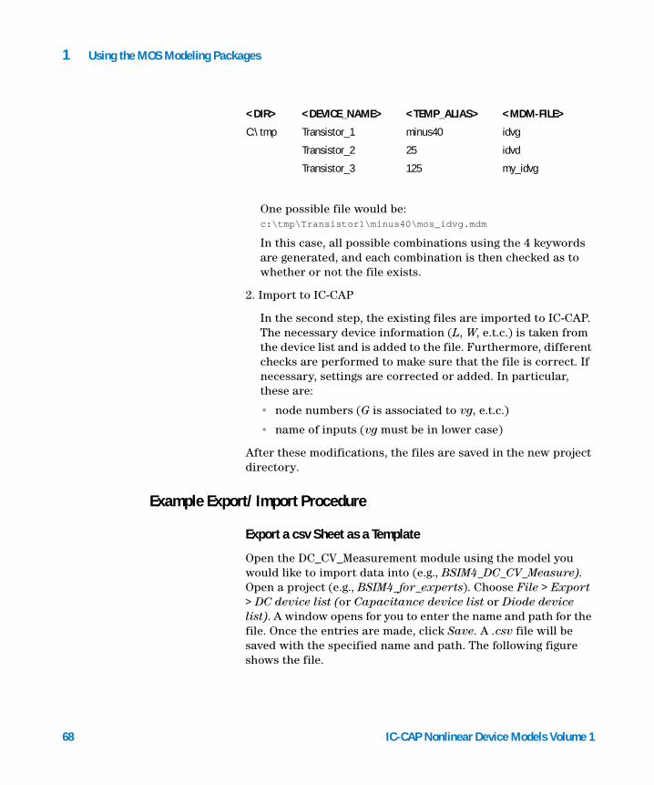
1 Using the MOS Modeling Packages
<DIR> <DEVICE_NAME> <TEMP_ALIAS> <MDM-FILE>
C:\tmp Transistor_1 minus40 idvg
Transistor_2 25 idvd
Transistor_3 125 my_idvg
68
One possible file would be: c:\tmp\Transistor1\minus40\mos_idvg.mdm
In this case, all possible combinations using the 4 keywords are generated, and each combination is then checked as to whether or not the file exists.
2. Import to IC-CAP
In the second step, the existing files are imported to IC-CAP. The necessary device information (L, W, e.t.c.) is taken from the device list and is added to the file. Furthermore, different checks are performed to make sure that the file is correct. If necessary, settings are corrected or added. In particular, these are:
• node numbers (G is associated to vg, e.t.c.)
• name of inputs (vg must be in lower case)
After these modifications, the files are saved in the new project directory.
Example Export/Import Procedure
Export a csv Sheet as a Template
Open the DC_CV_Measurement module using the model you would like to import data into (e.g., BSIM4_DC_CV_Measure). Open a project (e.g., BSIM4_for_experts). Choose File > Export > DC device list (or Capacitance device list or Diode device list). A window opens for you to enter the name and path for the file. Once the entries are made, click Save. A .csv file will be saved with the specified name and path. The following figure shows the file.
IC-CAP Nonlinear Device Models Volume 1
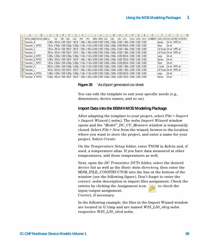
Using the MOS Modeling Packages 1
IC-CAP Nonlinear Device Models Vo
Figure 25 Via Export generated csv sheet
You can edit the template to suit your specific needs (e.g., dimensions, device names, and so on).
Import Data into the BSIM4 MOS Modeling Package
After adapting the template to your project, select File > Import > Import Wizard (.mdm). The mdm Import Wizard window opens and the “Model”_DC_CV_Measure window is temporarily closed. Select File > New from the wizard, browse to the location where you want to store the project, and enter a name for your project. Select Create.
On the Temperature Setup folder, enter TNOM in Kelvin and, if used, a temperature alias. If you have data measured at other temperatures, add those temperatures as well.
Next, open the DC Transistor DUTs folder, select the desired device list as well as the Basic data directory, then enter the MDM_FILE_CONSTRUCTOR into the line at the bottom of the window (see the following figure). Don’t forget to enter the correct .mdm description in import files assignment. Check the entries by clicking the Assignment icon to check the input/output assignment. Correct, if necessary.
In the following example, the files in the Import Wizard window are located in G:\tmp and are named W25_L50_idvg.mdm respective W25_L50_idvd.mdm.
lume 1 69
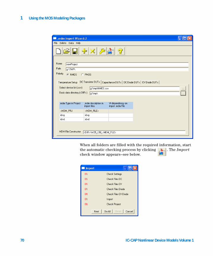
70
1 Using the MOS Modeling Packages
When all folders are filled with the required information, start the automatic checking process by clicking . The Import check window appears—see below.
IC-CAP Nonlinear Device Models Volume 1
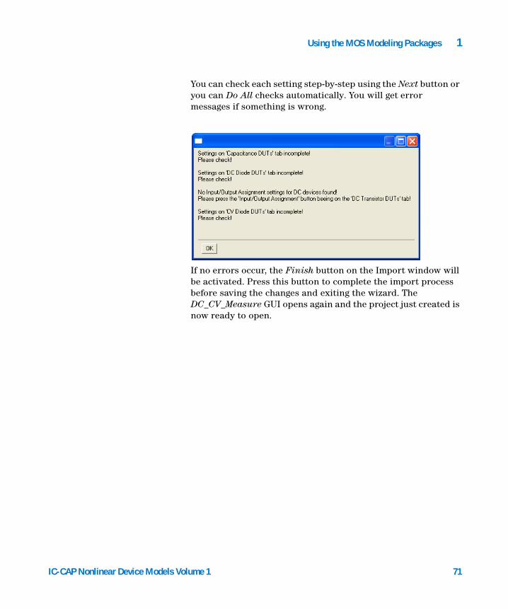
Using the MOS Modeling Packages 1
IC-CAP Nonlinear Device Models Vo
You can check each setting step-by-step using the Next button or you can Do All checks automatically. You will get error messages if something is wrong.
If no errors occur, the Finish button on the Import window will be activated. Press this button to complete the import process before saving the changes and exiting the wizard. The DC_CV_Measure GUI opens again and the project just created is now ready to open.
lume 1 71
1 Using the MOS Modeling Packages
RF Measurement
72
This section provides information on RF measurements using the BSIM3/BSIM4/PSP Modeling Packages. Starting the RF module opens a GUI divided into a number of folders for each task. The top row icons are the same as in the DC and CV measurement module. Assuming that you are already familiar with the functions of these buttons, we will not describe their purpose. You can easily check their use in “DC and CV Measurement of MOSFET’s for the MOS Models” on page 23.
RF Measurement Notes
The RF measurement module also contains a Notes folder to take notes on the project. It has the same look as the Notes folder of the DC/CV-measurement module, see “Project Notes” on page 26.
RF Measurement Conditions
The first task during RF modeling is to set up measurement conditions. Use the Measurement Conditions folder shown in the following figure to enter the measurement conditions at which you would like to measure and extract RF parameters.
IC-CAP Nonlinear Device Models Volume 1
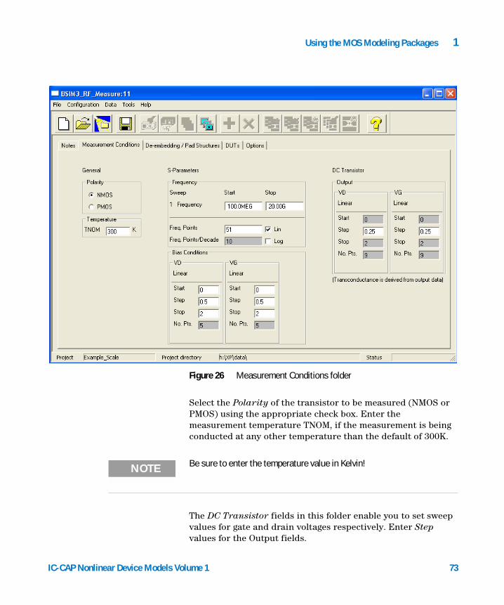
Using the MOS Modeling Packages 1
IC-CAP Nonlinear Device Models Vo
Select the Polarity of the transistor to be measured (NMOS or PMOS) using the appropriate check box. Enter the measurement temperature TNOM, if the measurement is being conducted at any other temperature than the default of 300K.
Figure 26 Measurement Conditions folder
NOTE Be sure to enter the temperature value in Kelvin!
The DC Transistor fields in this folder enable you to set sweep values for gate and drain voltages respectively. Enter Step values for the Output fields.
lume 1 73

74
1 Using the MOS Modeling Packages
The purpose of this field is to define measurement of DC characteristics of multifinger transistors used for RF NWA measurements. This step is necessary, since the DC behavior of a multifinger transistor differs from that of a single finger transistor. During DC measurement and extraction, a single finger transistor is being used, whereas a multifinger transistor is used in RF measurements to deliver sufficient drain currents for network analyzers to improve the measurement accuracy. Actual transistor DC measurements are used to set start points for S-parameters at low frequencies and control extraction at those points.
NOTE It is necessary to use the same values of start, stop, and step voltages for RF measurements as have been used for DC measurements. This is because it might be difficult for the optimizer to find parameter optimums during extraction, if the operating points differ in DC and RF measurements, since DC values are used as starting points for RF extractions.
Figure 27 S-parameter part of the Measurement Conditions folder
IC-CAP Nonlinear Device Models Volume 1
Using the MOS Modeling Packages 1
IC-CAP Nonlinear Device Models Vo
The Measurement Conditions folder provides fields to enter conditions for S-Parameter measurements. Enter Start and Stop frequency, choose the desired sweep (Linear or Logarithmic) and enter the number of Frequency Points to be measured during linear sweep or the number of Frequency Points/Decade for logarithmic sweep. Only the field ahead of the chosen sweep type (Lin or Log) is enabled allowing data to be entered.
Use the field Bias Conditions to enter sweep voltage Start, Step, and Stop values for drain and gate voltages during S-Parameter measurements.
For extraction purposes, VD/VG steps should lead an integer value.
De-embedding/Pad StructuresNOTE Be careful not to exceed the maximum DC Input voltage of the Network Analyzer used during measurements!
The De-embedding/Pad Structures folder enables you to select the type of pad structure used for de-embedding the parasitics of the measurements. Measurement of the transistors for parameter extraction requires connecting the devices to the instruments. Therefore, the basic transistor element to be measured must be connected using pads and metal connections on the wafer. In order to get the parameters of the basic transistor without metal connections and pads, the parasitics must be de-embedded from measurement results. A device library should contain only the basic transistor element. The connections to other elements in a circuit have to be modeled separately since this is part of the interconnection between elements on a chip.
Basically, you perform error correction of your network analyzer in order to eliminate measurement errors resulting from cable connections used to interface the analyzer to the wafer prober and up to the probe tips. Your test chip design
lume 1 75
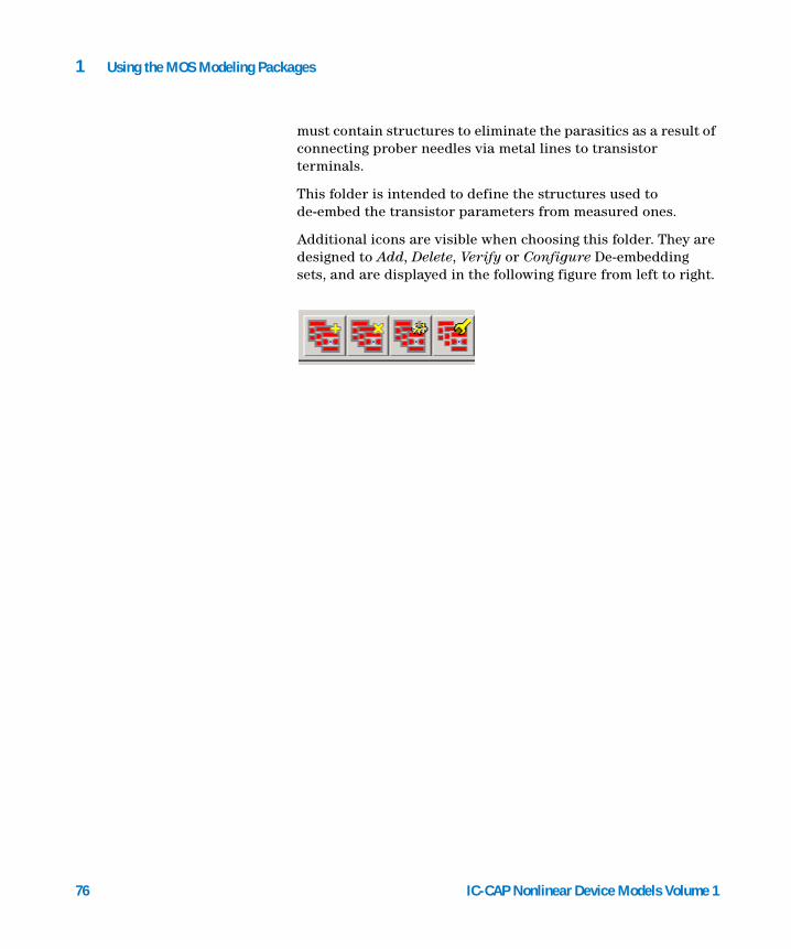
76
1 Using the MOS Modeling Packages
must contain structures to eliminate the parasitics as a result of connecting prober needles via metal lines to transistor terminals.
This folder is intended to define the structures used to de-embed the transistor parameters from measured ones.
Additional icons are visible when choosing this folder. They are designed to Add, Delete, Verify or Configure De-embedding sets, and are displayed in the following figure from left to right.
IC-CAP Nonlinear Device Models Volume 1
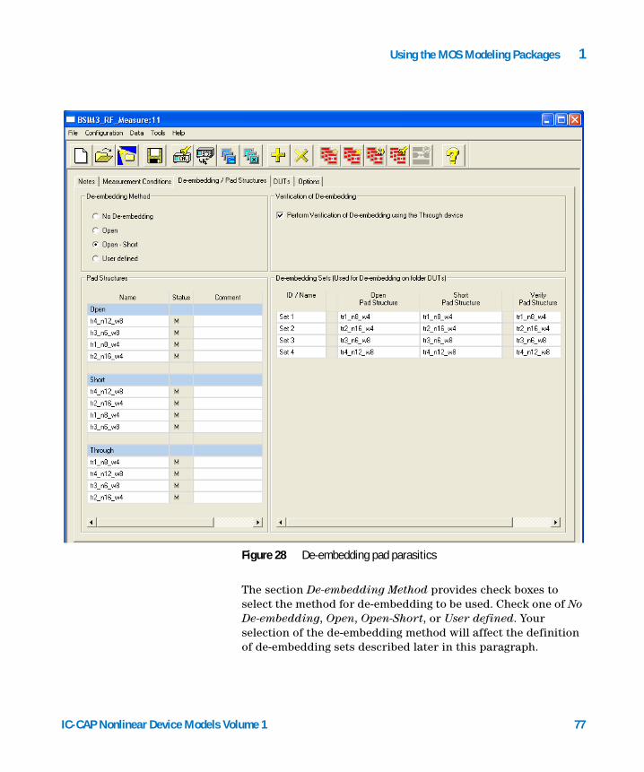
Using the MOS Modeling Packages 1
IC-CAP Nonlinear Device Models Vo
The section De-embedding Method provides check boxes to select the method for de-embedding to be used. Check one of No De-embedding, Open, Open-Short, or User defined. Your selection of the de-embedding method will affect the definition of de-embedding sets described later in this paragraph.Figure 28 De-embedding pad parasitics
lume 1 77
78
1 Using the MOS Modeling Packages
There is a section Verification of De-embedding where you can check a box to perform verification of de-embedding using the through device, if applicable.
The field Pad Structures is intended to declare dummy pads for de-embedding purposes. Click the Add icon and select the type of pad by clicking Open, Short, or Through on the appearing window, see below.
A new line will be inserted inside the field Pad Structures. You can change the name of the dummy pads as you like. The following rows are showing the status (not measured, showing “0”, measured, showing “M” or not applicable, showing “-”) as well as a user comment.
The Data > Measure menu is used to perform the measurement of the defined pads. Or you can press the Measure icon and select the pad you would like to measure in the appearing Measure form before clicking Measure DUT.
After the measurement has been performed, plots can be displayed using the appropriate icon or menu function, so that the measured results could be checked for plausibility of the measured data. Click the Close Plots icon to close the displayed plots of measured pads.
You can view the measured pad data at any time after a measurement has been performed by clicking Display Plots under the Data menu, or the appropriate icon, then selecting the pad to be displayed. The data will be displayed on Smith charts and can be closed using the Close Plots icon or the Data menu.
If you have chosen to perform a Verification of de-embedding by activating the Perform Verification of de-embedding Using... check box on the top right part of the folder, the field De-embedding Sets is being activated and you are able to configure the sets for use within the DUTs folder. Save the settings before configuring de-embedding sets.
A de-embedding set actually is a combination of pad structures to be use for de-embedding of measured devices. They can be used for one or more devices and can consist of any available pad structure.
IC-CAP Nonlinear Device Models Volume 1

Using the MOS Modeling Packages 1
IC-CAP Nonlinear Device Models Vo
Click the Add De-embedding Set icon once for each set to be used. A line for each set will be added. You are able to overwrite the predefined name of the sets.
Click the Configure/Allocate icon to assign a pad structure to a selected de-embedding set on the Configuration of de-embedding Sets form. Depending on the type of de-embedding you have chosen (No de-embedding, Open, Short or User Defined) in the De-embedding Method part of this folder, you are able to assign the respective pads to the sets. In other words, if you select Open as the de-embedding method, you can passing only pads of type Open to selected de-embedding sets. If you select Open-Short or User defined, you are able to assign pads of type Open, Short and Through to a set.
You can select the check box Perform Verification of De-embedding using the Through device if you have a Through device available on your test chip. Only after activating the verification, you can click the Verify Set icon to perform the verification of a selected set.
lume 1 79
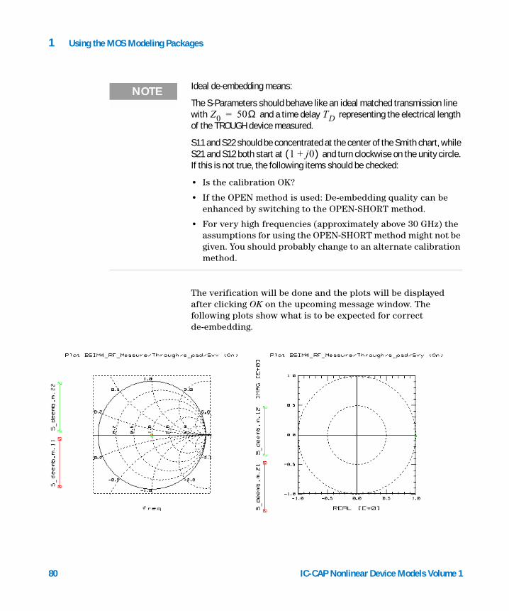
1 Using the MOS Modeling Packages
NOTE Ideal de-embedding means:
The S-Parameters should behave like an ideal matched transmission line with and a time delay representing the electrical length of the TROUGH device measured.
S11 and S22 should be concentrated at the center of the Smith chart, while S21 and S12 both start at and turn clockwise on the unity circle. If this is not true, the following items should be checked:
• Is the calibration OK?
• If the OPEN method is used: De-embedding quality can be enhanced by switching to the OPEN-SHORT method.
• For very high frequencies (approximately above 30 GHz) the assumptions for using the OPEN-SHORT method might not be given. You should probably change to an alternate calibration method.
Z0 50Ω= TD
1 j0+( )
80
The verification will be done and the plots will be displayed after clicking OK on the upcoming message window. The following plots show what is to be expected for correct de-embedding.
IC-CAP Nonlinear Device Models Volume 1
Using the MOS Modeling Packages 1
IC-CAP Nonlinear Device Models Vo
An error message will show up if one of the sets is not configured correctly.
After the de-embedding is done, you can assign the appropriate pad sets on the DUTs folder to their respective devices.
De-embedding of Parasitic Structures
The section “Test Structures for CV Measurements” on page 425 describes the effects of de-embedding. It is intended to give you an insight into de-embedding methods and describes the results of S-Parameter measurements with and without de-embedding.
DUTs
The DUTs folder is used to define transistor geometries for the DUT to be measured. Following the column for entering the name of the DUT, there is a column showing the status of the DUT. This column shows “0” if no measurement and de-embedding has been performed. It changes to “M” if a measurement has been performed and to “M, D” if measurement and de-embedding has been done. The geometries to be entered into the following columns are Width and Length of the transistor, Number of transistor Fingers (NF), Drain and Source Area and Perimeter Length (AD, AS, PD, PS). If the appropriate check boxes are checked or if the menu item Configuration > Geometric Entries has been set to GEOMOD=0, RGEOMOD=0 or NRS=0, NRD=0 and so on, the model selectors GEOMOD and RGEOMOD appear as a column (applicable to BSIM4/PSP only), and are set to their default values (0). The columns NRS, NRD and MIN are originally BSIM4 parameters, but are used also inside the extended BSIM3 model from AdMOS.
NOTE W, AD, AS, PD, and PS are total values including all fingers of the device!
There are two newly introduced instance parameters: Blocks (Number of Blocks) and NGCON (Number of Gate contacts). The Blocks parameter is actually a multiplier for the transistor. The other parameters (L, W, AD, AS ...) refer to Blocks = 1. The
lume 1 81
82
1 Using the MOS Modeling Packages
second new parameter, NGCON, defines the number of Gate contacts a transistor actually has, thus reducing resistance, for example. Those parameters can be activated or deactivated using the menu Configuration > Geometric Entries. By default, both parameters are on and set to 1. If they are set to off, the columns inside the DUTs folder will not be present.
NOTE The DUTs folder looks the same for BSIM3 and BSIM4/PSP. However, this folder contains some parameters and model flags that are only applicable for BSIM4/PSP. The default values for parameters not used in BSIM3 are set in such a way, that BSIM3 ignores them. This is done to make the form compatible for both models.
In BSIM4, the model selector GEOMOD is used to select a geometry-dependent parasitics model that specifies whether the end source/drain diffusions are connected or not. The default value is (0) — not connected. The parameter RGEOMOD is the source/drain diffusion resistance model selector. It specifies the type of end source/drain diffusion contact type: point, wide or merged contact. The default value is (0) — no source/drain diffusion resistance. See the BSIM4 manual from UC Berkeley [1] on page 11-5 and 11-6 for a definition of GEOMOD and RGEOMOD model selector values.
The parameters NRS, NRD and MIN are the layout dependent parameters Number of Source/Drain diffusion squares and Minimization of diffusion squares for even numbered devices. They are set to their default values (0), too.
The last column enables you to enter a comment for this DUT.
IC-CAP Nonlinear Device Models Volume 1
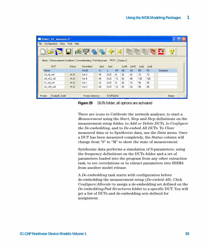
Using the MOS Modeling Packages 1
IC-CAP Nonlinear Device Models Vo
There are icons to Calibrate the network analyzer, to start a Measurement using the Start, Stop and Step definitions on the measurement setup folder, to Add or Delete DUTs, to Configure the De-embedding, and to De-embed All DUTs. To Clear measured data or to Synthesize data, use the Data menu. Once a DUT has been measured completely, the Status column will change from “0” to “M” to show the state of measurement.
Synthesize data performs a simulation of S-parameters, using the frequency definitions on the DUTs folder and a set of parameters loaded into the program from any other extraction task, to see correlations or to extract parameters into BSIM4 from another model release.
A De-embedding task starts with configuration before de-embedding the measurement setup (De-embed All). Click Configure/Allocate to assign a de-embedding set defined on the De-embedding/Pad Structures folder to a specific DUT. You will get a list of DUTs and de-embedding sets defined for assignment.
Figure 29 DUTs folder, all options are activated
lume 1 83
84
1 Using the MOS Modeling Packages
Click the DUT, then click the SET to be assigned to the selected DUT.
Click the De-embed All icon to start de-embedding measured data for each DUT with a de-embedding set assigned.
The Display Plots icon is intended to check the measurement results in the form of diagrams, using the settings made on the Options folder. You can Display and Close Plots using the appropriate icon for this task.
Select the plots you would like to see or view all plots in one window.
RF Measurement Options
Using this folder, you can set the size of the plot window to fixed. See “Options” on page 65 for details.
IC-CAP Nonlinear Device Models Volume 1
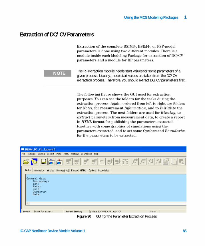
Using the MOS Modeling Packages 1
Extraction of DC/CV Parameters
IC-CAP Nonlinear Device Models Vo
Extraction of the complete BSIM3-, BSIM4-, or PSP-model parameters is done using two different modules. There is a module inside each Modeling Package for extraction of DC/CV parameters and a module for RF parameters.
NOTE The RF extraction module needs start values for some parameters of a given process. Usually, those start values are taken from the DC/CV extraction process. Therefore, you should extract DC/CV parameters first.
The following figure shows the GUI used for extraction purposes. You can see the folders for the tasks during the extraction process. Again, ordered from left to right are folders for Notes, for measurement Information, and to Initialize the extraction process. The next folders are used for Binning, to Extract parameters from measurement data, to create a report in HTML format for publishing the parameters extracted together with some graphics of simulations using the parameters extracted, and to set some Options and Boundaries for the parameters to be extracted.
Figure 30 GUI for the Parameter Extraction Process
lume 1 85
86
1 Using the MOS Modeling Packages
The top row of the GUI window contains a menu to perform file operations like Open, Examples, Save Setup/Entries, Export and Import Extraction, and Batch Processing. The next menu items are used to Initialize extractions, to set Binning items and Extract options, to show Plots, to create HTML reports, to set Options and Boundaries, and to call the Help menu. The Help menu gives access to specific help for the different tasks during extraction of parameters. You’ll find help for each folder of the BSIM Modeling Packages as well as a list of topics. The Info menu item provides some information about the BSIM Modeling Package like version, date, and its creators—AdMOS.
You can find most of the menu settings in the form of icons just below the menu. Some icons are only activated for specific tasks.
At the bottom of the extract window, you can find the project name and project directory used for the extraction.
Using the File > Examples menu, a form opens to let you copy an example project to a path and a location where you have write access. This step is necessary, since the IC-CAP example directories are usually write protected and you need write access to modify the example files.
If you would like to Open an existing project, select the project path and name in the Open Project dialog box. Using Export Extraction opens the Export Extractions form which enables you to choose path and name of the saved extraction settings file. It is not possible to create a non-existing path on Windows. Instead, you must create the desired folders, if non-existent, using the Windows Explorer.
NOTE Opening a project takes some time. You are able to reduce this time by saving the complete ~.mdl file. Reloading the ~.mdl file is faster than opening a project. However, since the ~.mdl file contains a large amount of data which is already stored somewhere in the system, you need to have extra storage capacity on your hard disc.
IC-CAP Nonlinear Device Models Volume 1
Using the MOS Modeling Packages 1
IC-CAP Nonlinear Device Models Vo
You are able to Import Extractions by selecting the path and name of the saved extraction settings file inside the Import Extractions dialog box. This might be useful, for example, if you found a special extraction sequence that best fulfills the need of your parameter extraction process. You save those sequence by exporting the settings to a file and using this file as template for following extraction processes.
NOTE Importing extraction settings will overwrite the actual settings within the active extraction process!
The Batch Processing menu option enables you to run extractions overnight, for example. It is possible to specify the path and name of several projects for extraction or for generation of HTML reports.
The tasks to be performed are ordered using different folders from the left to the right side of the BSIM3/4_extract window. They should be performed in this manner. Some of the folders have default values for your convenience. If you are satisfied with the defaults, those folders could be left as they are. However, you are not required to follow this order.
DC Notes
There is a folder provided to take some Notes on the project. It has the same look as the one used in the Measurement modules—see Figure 5 on page 32, for example.
DC Information
NOTE This folder is intended for notes on extraction. It will not overwrite your notes entered and saved during the measurement session. These are kept in the information folder.
The next folder to the right gives you Information about the devices measured (see the following figure). You’ll find the type of MOSFET, measurement temperatures, DUT names together
lume 1 87
88
1 Using the MOS Modeling Packages
with their geometries and categories as well as the notes entered during the measurement. If no measurement was performed on any of the DUTs, there will be a notice stating the incomplete measurement status at the end of the line for that DUT.
NOTE It is not possible to change the measurement information during the extraction session. This folder is for information on measurements only!
Figure 31 Information Folder during Extraction
IC-CAP Nonlinear Device Models Volume 1
Using the MOS Modeling Packages 1
DC Initialize
IC-CAP Nonlinear Device Models Vo
The folder Initialize (Figure 32 for BSIM3 and Figure 33 for BSIM4/PSP) is intended to set initial conditions for parameter extraction. Since the initial conditions for BSIM3 and BSIM4/PSP models differ, the following section shows both Initialize folders, one after the other.
BSIM3
The Initial Values section of the folder contains fields for Model Parameters and Model Flags. Into the field Model Parameters, enter process related parameters like oxide thickness (TOX) or doping concentrations (channel doping concentration NCH respective gate doping concentration NGATE), and so on. Entering values into the fields and selecting Save starts a routine to check the values entered. This routine will flag an error message and change the color of the field whose
Figure 32 Initialize folder to set initial conditions for the extraction of BSIM3 parameters
lume 1 89
90
1 Using the MOS Modeling Packages
parameter is given an unrealistic value. The specific field will be marked with red color and remains red until the value is corrected.
The Model Flags section is used to set BSIM3 model flags. There are fields for global model flags like BINUNIT or PARAMCHK as well as fields for DC/Capacitance and Noise model flags. The model flags are set to a default value as has been described in the BSIM3 manual from UC Berkeley [1]. See “Model Selection Flags” on page 419 for details or the above mentioned UCB manual [1].
If you are using HSPICE, a field is provided to set parameters for Gate current extraction.
A section called Initial Parameter Set is located below the Initial Values section. You can use a parameter set from any other extraction with IC-CAP, a circuit simulator (.cir) file, or a text (.model) file. Using the .cir or .model file requires you to specify an appropriate simulator. You enter the required information using the menu Initialize > Initial Parameter Set > Add. The form that opens enables you to enter the necessary information, browse to the file location, and select the simulator.
To change between using the Initial Values and Initial Parameter Sets, select the radio button to the left of each section. Select which initialization procedure you want to use.
If you would like to use the binning capability, check the Generate Binning Model button. With this button checked, the folder Binning is activated.
There is a field provided to enter PEL commands, which are executed at initialization of the extraction process.
Note that the sequence of initialization uses values of the model parameters first, before PEL commands are executed.
From the menu Initialize, chose Set Initial Values to Circuit Defaults if you would like to reset the parameters.
IC-CAP Nonlinear Device Models Volume 1
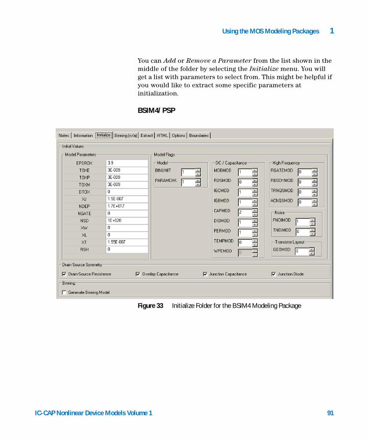
Using the MOS Modeling Packages 1
IC-CAP Nonlinear Device Models Vo
You can Add or Remove a Parameter from the list shown in the middle of the folder by selecting the Initialize menu. You will get a list with parameters to select from. This might be helpful if you would like to extract some specific parameters at initialization.
BSIM4/PSP
Figure 33 Initialize Folder for the BSIM4 Modeling Package
lume 1 91
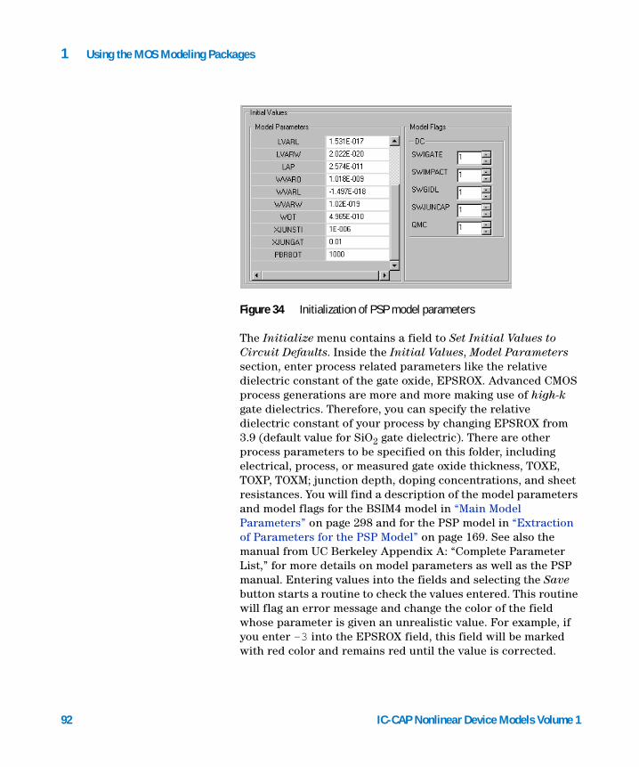
92
1 Using the MOS Modeling Packages
Figure 34 Initialization of PSP model parameters
The Initialize menu contains a field to Set Initial Values to Circuit Defaults. Inside the Initial Values, Model Parameters section, enter process related parameters like the relative dielectric constant of the gate oxide, EPSROX. Advanced CMOS process generations are more and more making use of high-k gate dielectrics. Therefore, you can specify the relative dielectric constant of your process by changing EPSROX from 3.9 (default value for SiO2 gate dielectric). There are other process parameters to be specified on this folder, including electrical, process, or measured gate oxide thickness, TOXE, TOXP, TOXM; junction depth, doping concentrations, and sheet resistances. You will find a description of the model parameters and model flags for the BSIM4 model in “Main Model Parameters” on page 298 and for the PSP model in “Extraction of Parameters for the PSP Model” on page 169. See also the manual from UC Berkeley Appendix A: “Complete Parameter List,” for more details on model parameters as well as the PSP manual. Entering values into the fields and selecting the Save button starts a routine to check the values entered. This routine will flag an error message and change the color of the field whose parameter is given an unrealistic value. For example, if you enter -3 into the EPSROX field, this field will be marked with red color and remains red until the value is corrected.
IC-CAP Nonlinear Device Models Volume 1
Using the MOS Modeling Packages 1
IC-CAP Nonlinear Device Models Vo
You are able to add BSIM4/PSP parameters to the Initial Values by clicking Add Parameter inside the Initialize menu. You will be prompted with a list of BSIM4/PSP parameters. Select the parameters you would like to add and click OK. The parameters are added and you are able to enter initial values as desired.
The Model Flags section is used to set BSIM4/PSP model flags. The fields only enable settings as defined in the BSIM4/PSP model and are predefined to standard settings.
There is a field defining the symmetry of the drain and source areas. Check the appropriate box(es) if drain and source are processed using the same dose of implantation as well as the same geometry, and therefore the parameters are equal for drain and source areas.
Binning
NOTE Since most MOS processes use symmetric source and drain processing parameters, there is no need to extract the parameters for the bulk-source or bulk-drain diodes separately. Instead, check that the symmetry fields and the respective parameters are set equally.
Only for unsymmetrical processes, which could be modeled in BSIM4/PSP, the fields remain unchecked and a separate parameter set will be extracted for bulk-source and bulk-drain diodes.
You will find some theory on binning inside “Binning of Model Parameters” on page 452. The following figure shows the Binning folder, used in binning model parameters. This folder is active only if the flag Generate Binning Model is checked, otherwise you will find an n/a sign next to the folder name. This flag is located on the Initialize folder under Generate Binning Model.
lume 1 93
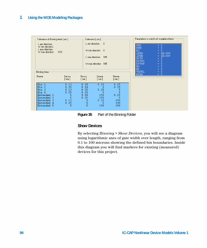
94
1 Using the MOS Modeling Packages
Show DevicesBy selecting Binning > Show Devices, you will see a diagram using logarithmic axes of gate width over length, ranging from 0.1 to 100 microns showing the defined bin boundaries. Inside this diagram you will find markers for existing (measured) devices for this project.
Figure 35 Part of the Binning Folder
IC-CAP Nonlinear Device Models Volume 1

Using the MOS Modeling Packages 1
IC-CAP Nonlinear Device Models Vo
Set Bin
Select bin boundaries by using the displayed diagram, marking two adjacent corners of a rectangle representing the bin and choose Set Bin from the Binning menu. Be sure to include devices at every corner of your bin, otherwise you will get an error message stating that the selected bin is not rectangular. See the figures below for clarification.
Figure 36 Diagram of measured devices (red), extension devices (blue) and binned devices (magenta)
lume 1 95
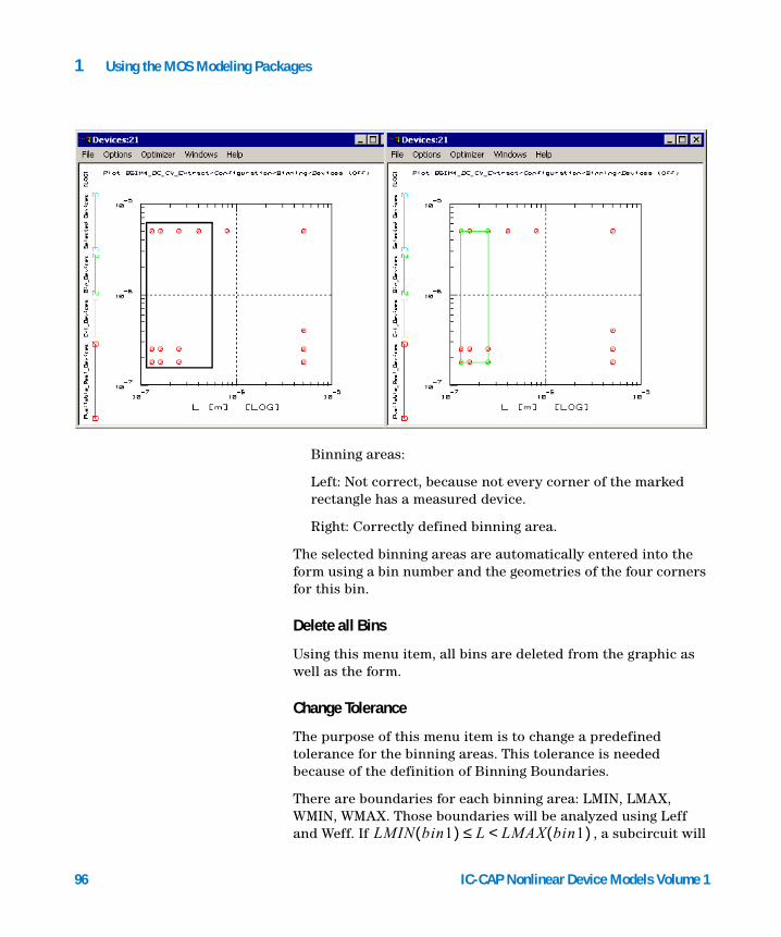
96
1 Using the MOS Modeling Packages
Binning areas:
Left: Not correct, because not every corner of the marked rectangle has a measured device.
Right: Correctly defined binning area.
The selected binning areas are automatically entered into the form using a bin number and the geometries of the four corners for this bin.
Delete all Bins
Using this menu item, all bins are deleted from the graphic as well as the form.
Change Tolerance
The purpose of this menu item is to change a predefined tolerance for the binning areas. This tolerance is needed because of the definition of Binning Boundaries.
There are boundaries for each binning area: LMIN, LMAX, WMIN, WMAX. Those boundaries will be analyzed using Leff and Weff. If , a subcircuit will LMIN bin1( ) L LMAX bin1( )<≤
IC-CAP Nonlinear Device Models Volume 1
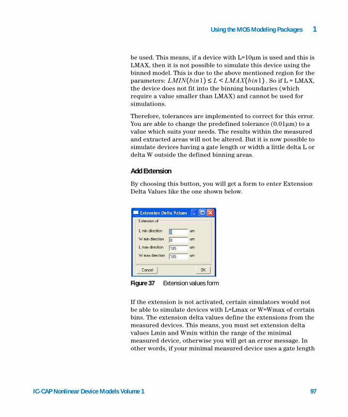
Using the MOS Modeling Packages 1
IC-CAP Nonlinear Device Models Vo
be used. This means, if a device with L=10µm is used and this is LMAX, then it is not possible to simulate this device using the binned model. This is due to the above mentioned region for the parameters: . So if L = LMAX, the device does not fit into the binning boundaries (which require a value smaller than LMAX) and cannot be used for simulations.
Therefore, tolerances are implemented to correct for this error. You are able to change the predefined tolerance (0.01µm) to a value which suits your needs. The results within the measured and extracted areas will not be altered. But it is now possible to simulate devices having a gate length or width a little delta L or delta W outside the defined binning areas.
Add Extension
By choosing this button, you will get a form to enter Extension Delta Values like the one shown below.
If the extension is not activated, certain simulators would not be able to simulate devices with L=Lmax or W=Wmax of certain bins. The extension delta values define the extensions from the measured devices. This means, you must set extension delta values Lmin and Wmin within the range of the minimal measured device, otherwise you will get an error message. In other words, if your minimal measured device uses a gate length
Figure 37 Extension values form
LMIN bin1( ) L LMAX bin1( )<≤
lume 1 97
98
1 Using the MOS Modeling Packages
of 0.15µm, the extension in Lmin direction must be set between 0 and 0.149µm. There is no limit for the extension in the Lmax and Wmax direction.
If you select one of the defined bins, the fields under Devices in Bin<No> will become green shaded and will show the name of the corner devices of this bin and the corner geometries, see Figure 35. At the same time, the diagram will show the selected bin boundaries in light blue color.
Delete Extension
You can delete the entered extensions by choosing the menu item Binning > Delete Extension button.
The field Parameters to switch off scalable effects is used to set which parameters use the scalable possibilities as defined inside the BSIM4/PSP model and which parameters are prevented from scalable modeling in BSIM4/PSP. All deselected parameters are using the extracted values, whereas all selected parameters (marked with blue background) are using default values for binning purposes. The parameters DWG and DWB are always off, therefore they cannot be de-selected.
DC Extract
The next folder, Extract, defines the Extraction Flow for the devices. There is a standard extraction flow implemented, but you can change this flow if you find another one suiting your needs better than the default one.
The PSP model extraction flow is somewhat different, since it extracts local and global parameters in alternating steps, although the handling is the same. It is described in detail under “Extraction of Parameters for the PSP Model” on page 169.
You can also add custom extraction steps using a feature called Finetuning. See “Finetune” on page 111.
IC-CAP Nonlinear Device Models Volume 1
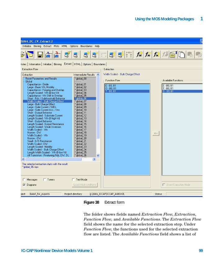
Using the MOS Modeling Packages 1
IC-CAP Nonlinear Device Models Vo
The folder shows fields named Extraction Flow, Extraction, Function Flow, and Available Functions. The Extraction Flow field shows the name for the selected extraction step. Under Function Flow, the functions used for the selected extraction flow are listed. The Available Functions field shows a list ofFigure 38 Extract form
lume 1 99
100
1 Using the MOS Modeling Packages
functions to be used for a selected extraction flow. Mark the desired function and click the arrow in between the Function Flow and Available Functions fields to add the function to the flow list. The letters in front of the function name explain the extraction method used for this function: E represents extraction, O stands for optimization, and T for tuning.
The extraction list inside the field Extraction is organized into two main groups to provide a better overview when using a large number of steps or devices for extraction. This is done by introducing extraction groups for Global or Binning extraction, and hiding or expanding the list of extraction groups (for global extractions) respective to the list of devices (for binning extractions).
You can select the dependency from L, W, and P (L*W) for some of the parameters using the Extract > Edit Global Binning Parameter menu. A window opens up, where you can check parameters and dependencies to acknowledge during the global binning process.
Predefined extractions or optimizations for global binning parameters are not available. You can configure optimizations for global binning parameters in two ways:
• Generate a plot optimizer (see page 113) and invoke it in the group Finetuning inside the extraction flow.
• Manually add global binning parameters to predefined optimizers. This change is saved as a user defined customization.
You can set initial conditions for binning using the Extract > Extraction Flow > Initial Conditions menu or clicking the appropriate icon from the icon bar.
A window opens enabling you to configure full parameter sets for each device from other devices and add single parameters to this global binning extraction step from a list of parameters. You can select the intermediate results to use from a drop down list at the bottom of the Add Starting Parameters window that shows already extracted devices up to this stage of extractions. You are also able to delete single parameters from the list.
IC-CAP Nonlinear Device Models Volume 1
Using the MOS Modeling Packages 1
NOTE Global binning in this context means, there is the possibility to extract some parameters in a more global way. The device parameters are already extracted, now you are interested in geometrical influences on some parameters. Binning in the usual way recognizes dependencies on device length and width, represented through bins. Those bins represent ranges of lengths and widths of the devices. However, global binning uses no bins, but tries to extract the influences over length (parameter L), width (parameter W), and the product of L*W (parameter P). Using this feature, it is possible, for example, to represent a normally not on length and width depending parameter like VTH0 in a geometry dependent way through extraction over several different devices in this global binning approach!
IC-CAP Nonlinear Device Models Vo
Using the menu Extract > Extraction Flow, there are buttons to Add or Delete Extractions from the flow. There are icons provided for these actions too. You will be prompted with a list of available extractions. Select one of the extraction steps and press Add on that form. If you have already extracted parameters, the Extraction Status field shows intermediate steps. This will show which results are being used for the selected extraction step. Now, if you Add or Delete, change the arrangement of the steps or reset to Defaults, the following extractions will become invalid because they are based on the results of the extraction immediately before them. Therefore, you will be warned before changes are made!
lume 1 101

102
1 Using the MOS Modeling Packages
Arranging the flow is possible by using the Move Up or Move Down buttons below the Function Flow or by using the icons provided.
To extract parameters from one flow only: Select the desired flow under the Extraction Flow section in the left half of this folder and choose Extract >Single Extraction. Again, you will be warned before the selected extraction will be performed.
To go through the extraction process one step at a time, highlight the step and choose Extract > Step by Step Extraction. A dialog box may appear, prompting you for input.
• To automatically extract all parameters using the extraction flows listed under the Extraction Flow section, choose Extract > Automatic Extraction. The programmed Extraction Flow will be extracting all parameters defined in the active extraction flow list. The programmed extraction flow has to begin with the Reset Parameters step, otherwise you will get an error message.
IC-CAP Nonlinear Device Models Volume 1
Using the MOS Modeling Packages 1
IC-CAP Nonlinear Device Models Vo
• In case you would start an extraction of some parameters after you already have extracted some other parameters, you are not able to start from the beginning without resetting all parameters, including the ones already extracted. To re-extract or to optimize one parameter after some other parameters are already extracted, simply add the desired step in the extraction flow list on a place further down the list. In that case, the extraction process uses the parameters already extracted during an earlier step in the extraction process and you overcome the reset parameter step.
• All warnings and errors during the extraction process are written to the failure log, which is opened using the Extract > Failure Log menu item.
NOTE The contents of the Failure Log window doesn’t contain all the warnings written to the IC-CAP status window. Only the warnings and errors regarding parameter extraction are re-directed to the Failure Log.
You can add several steps of the same extraction after each other. The extraction method selected in one step could be another one in a further extraction step. In other words, you are able to set the tuner option in one extraction step and the optimizer option in another step, probably when other parameters of influence have been extracted in between the steps.
• Change the function flow inside the Function Flow field using the Move Up or Move Down buttons below that section to move a selected extraction routine one step up or down.
• The Default button restores the order of parameter extractions inside the Function Flow list as it was in the beginning of a project.
• To delete an extraction from the Function Flow, choose Delete.
lume 1 103
1 Using the MOS Modeling Packages
NOTE You cannot delete the first (Reset Parameters) or the last (Save Parameters) extraction step inside an extraction flow.
104
• Below the Extraction Flow field, check boxes enable you to Deactivate Tuners or to use the Test Mode without saving the extracted parameters. This mode is intended for you to test influences of some parameters on others without overwriting already extracted parameters from the selected step. You are able to use every *.mps file with every extraction step without saving and resetting parameters.
You will notice the changing of colors on the Extraction Folder. This is a visual warning that intermediate results are not stored in this mode!
NOTE This feature makes it possible to test influences of any other *.mps file to compare extraction results.
Test mode starts with the last step taken in the flow. No results are overwritten or saved!
• To export the extracted parameters during the defined extraction flow for the purpose of saving intermediate results, use Export Extraction under the Extract menu. You must specify the path and the name for the parameter file to be exported. Exported files will be packed into a .tar file using the project name as a file name and appending Export and a number to the extracted .tar file. (~project_name~Export_1, for example)
• An item is provided under the Extract menu to Import Model Parameter Set, from an earlier project, for example. You will receive a warning message stating that importing parameters will overwrite the actual model parameters in IC-CAP.
Select either a Project or, if existing, an exported .tar file for a specific project. In this case, you must select the project as well as the exported extractions. Then you will be able to select whether you would like to use all or specific parts of the saved extraction project components by de-activating the components
IC-CAP Nonlinear Device Models Volume 1

Using the MOS Modeling Packages 1
IC-CAP Nonlinear Device Models Vo
not to be used (results, settings, boundaries and finetuning). If there are stored files, they will be shown under the Files section of this window.
NOTE This feature makes it possible to import any other *.mps file to compare results. But be careful, importing other parameter files will overwrite the actual parameters. Don’t use this option during an extraction session with partly extracted parameters unless you’ve saved the work in progress!
Interactive Extraction Mode
A new, powerful feature of IC-CAP and the BSIM Modeling Packages is the ability to display several plots in one window. It is called a Multiplot window. This feature is used when you enter the Interactive Extraction Mode. Either use the Extract menu or the interactive mode icon, , to invoke this mode.
The Interactive Extraction Mode opens a Multiplot window with a default number of plots shown. To the right of the interactive plot window, you can see three folders:
• Devices: This folder is used to select devices for extraction. You will find a list of devices as has been defined inside the measurement module, DC Transistor DUTs. Select one of the devices for extraction.
• Extract: This folder shows one or more parameters to be extracted during this extraction step. You can select a device of your choice within the Devices folder or use the Default button (to be found on Devices) to accept the default transistor suggested by AdMOS. To the left of the Interactive Plot window, the extraction step and the extraction function for the selected step are shown. Start extraction by clicking Execute. The parameters are extracted and the plot window shows the simulated diagrams together with the measured ones. Now you are able to Store the results or continue the extraction process without storing intermediate results. Use the >-button to go on to the next step inside the extraction flow or extract all parameters of this step using the >>-button.
lume 1 105
106
1 Using the MOS Modeling Packages
• During extraction of some parameters inside the Extract folder, the Region Boundaries section is activated. Then you are able to select a specific extraction region by using Show button. The upper left of the plots is now showing a rectangle. This is the region where extraction takes place. You are able to change the predefined extraction area by opening a rectangle in Plot 0 (the upper left plot) using the left mouse button. A rectangle is shown. If you are satisfied with the selected area, use the right mouse button and select Add Region. The added rectangle now changes color and is used as the extraction region for this step. Remove the rectangle (the defined region is still valid) by using Hide.
• The PEL button opens a window showing the default region calculation. This is done using the PEL language. Use this window to change the calculation by editing the values or changing the formulas used for calculation. Within this region calculation window, you are also able to reset any changes made using the Default button and/or to Accept and Show changes in Plot 0. Using OK, the selected or calculated region is accepted and used for this extraction step.
• The Store button enables you to store intermediate results. This is useful for a what-if-scenario. Once you’ve stored parameters, the selection field to the right of the Store button enables you to select either the stored parameters or the results of the default step to be used for the next extraction step. Each parameter set you’ve stored will be given an extraction number using the sequence of the extraction.
IC-CAP Nonlinear Device Models Volume 1

Using the MOS Modeling Packages 1
IC-CAP Nonlinear Device Models Vo
• If there is an optimizer step programmed during this extraction, the folder name changes from Extract to Optimize and there are fields to select optimizer features like Algorithm or Error. The Parameters field now enables you to enter parameter values manually by double clicking the parameter field and entering a value. You are also able to change boundaries of the parameters by using Autoset (the parameter value will be multiplied by 0.5 and 5 to determine the boundaries) or Reset (boundaries as have been defined inside IC-CAP model parameters window are used). Adopt will overwrite the standard IC-CAP values and the changed values are used for this extraction session.
• The Parameters field of this folder enables you to add parameters to this step using the blank parameter field below the predefined parameters used in this step. If you enter a valid BSIM parameter and press enter, the value of this parameter as has been extracted so far will be shown in the middle column.
• If you check the Save actual Optimizer Min/Max values check box, a new invocation of IC-CAP will use the changed boundaries, otherwise the standard values will be used again.
• You can enter an exclamation mark (!) in front of a parameter to temporarily deactivate a parameter without removing it from the list.
• Using the Tuner feature, this folder will change the name from Extract or Optimize to Parameter. The Parameters field of this folder has the same function as has been described for the optimizer above.
• The third folder now changes from n/a to Tuner. It shows the parameter tuner sliders for interactive tuning. The results of changing the slider positions will be shown immediately inside the plots. Again, you are able to store results under predefined names. You can use the results of this step or go on without the results of the tuning step.
lume 1 107
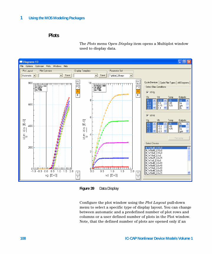
1 Using the MOS Modeling Packages
Plots
108
The Plots menu Open Display item opens a Multiplot window used to display data.
Configure the plot window using the Plot Layout pull-down menu to select a specific type of display layout. You can change between automatic and a predefined number of plot rows and columns or a user defined number of plots in the Plot window. Note, that the defined number of plots are opened only if an
Figure 39 Data Display
IC-CAP Nonlinear Device Models Volume 1
Using the MOS Modeling Packages 1
IC-CAP Nonlinear Device Models Vo
appropriate number of devices, outputs, or temperatures is selected. This means, if you manually set a plot display of 3x3 plots, select the IdVg-plot of one device at one temperature and one output, you will only see one plot! Choosing the Automatic plot layout displays the appropriate number of plots according to your selection!
To the right, you are able to select Devices, Bias Conditions, and Outputs to be plotted. Changes take place if you press Redisplay. Under the Plot menu of the Plot window, you can zoom in on a specific plot or get a full screen plot. You will be prompted for the plot to zoom to. This menu is also used to undo the display changes.
There is a pull-down menu, located below the top row of the multiplot window, named Display Template. It is used to store a set of displayed plots under a user specified name. This feature is intended to compare plots created with different extraction steps, for example. Arrange all plots you want to be stored, then press the save button and enter a name into the appearing window or accept the given one. To open an arrangement already saved, simply choose the one to be displayed from the Display Templates pull-down menu.
Folder Cycle Devices
Inside the Select Bias Condition area, select one or both diagram types: IdVg and/or IdVd. Then, click the desired voltages, temperatures, and outputs for the selected diagram types. You are able to mark one or more rows in each of the columns. To mark more than one voltage, temperature, or device, press and hold the left mouse button and select the items to be displayed.
The Select Device area shows the devices with the appropriate type of data according to your choice. For example, selecting a temperature other than room temperature will show only devices that are measured at those temperatures. Press Redisplay after you’ve made your choice.
A selection of more than one value of Vd or Temperature displays the chosen diagram (output) with a number of curves corresponding to your choice of Bias or Temperature.
lume 1 109
110
1 Using the MOS Modeling Packages
Folder Cycle Plot Types
This folder enables you to choose different data representations or to compare the diagrams of different devices. For example, you can add a second y-axis to any plot, adding - let’s say - the gate current to a diagram of the drain current vs. gate voltage.
If you selected a number of devices to be displayed using the same diagram for comparison and want to examine a curve that seems to be different from the others, you can zoom in on a plot. To zoom in on a plot, either select a plot and then Plots > Zoom Plot > Selected Plot from the menu of the multiplot window, or Zoom Plot or Full Page Plot and select one of the plots by number. The plots are numbered from top left to bottom right. The window changes in the Zoom Plot mode to one magnified plot and all other plots are displayed very small. In the Zoom Plot mode, you can jump to zoom another plot just by clicking the desired plot with the left mouse button. You can also select one curve of the chosen plot to be enhanced for reading voltages or currents from specific data points. Those currents and voltages are displayed above the diagram for the selected and marked data point.
Folder All Diagrams
Using this folder, you can display different plots to be compared or used for optimization. In contrast to the other folders of this window, you should define a Plot Layout first. If you select a 2x3-configuration, for example, you will get 6 empty plots inside the display area of the window. Click on one of those empty plots, open a menu by using the right mouse button and select Flexible Plot Configuration from this menu. Now you can select a predefined plot type from the All Diagrams folder and choose the desired voltages, axis settings, temperature, or devices to be displayed inside the selected plot. Using another plot, choose Transistor Capacitance > C oxide from the menu below the right mouse button, for example. This gives you the ability to mix plot types and devices in any configuration you’d like! For details, see the example provided in the following section.
IC-CAP Nonlinear Device Models Volume 1
Using the MOS Modeling Packages 1
Finetune
IC-CAP Nonlinear Device Models Vo
This feature enables you to add customized optimization steps. You can select one or more measured diagrams to create and save an extraction step in which to adjust certain parameters for a specific region of device behavior. This step can be inserted into the extraction flow at any desired step in the extraction procedure.
To use the finetuning feature, do the following:
• Open a Data Display.
• Select the desired Plot Types, Devices, and Bias Conditions to be displayed.
• Activate a diagram.
• Activate this diagram for optimization (PO button to the right of the diagram).
• Repeat the steps above for each plot you would like included in your finetuning step.
• Open the Plot Optimizer (right mouse button: Optimizer > Open Optimizer).
• From the parameter list of the Plot Optimizer, select the parameters you would like to finetune using the selected diagrams. Save your configuration.
• Once the configuration has been stored, it will be present inside the BSIM4/PSP GUI extract folder under Available Functions in the Finetuning step and can be inserted into the Function Flow.
The following is an example using this feature to extract the threshold voltage from two different types of plots.
• Open the Data Display (Menu: Plots > Open Display) and go to folder All Diagrams
• Select a 2x1 plot layout from the Plot Layout menu
• Select one of the plots, then use the right mouse button to access Flexible Plot Configuration.
lume 1 111
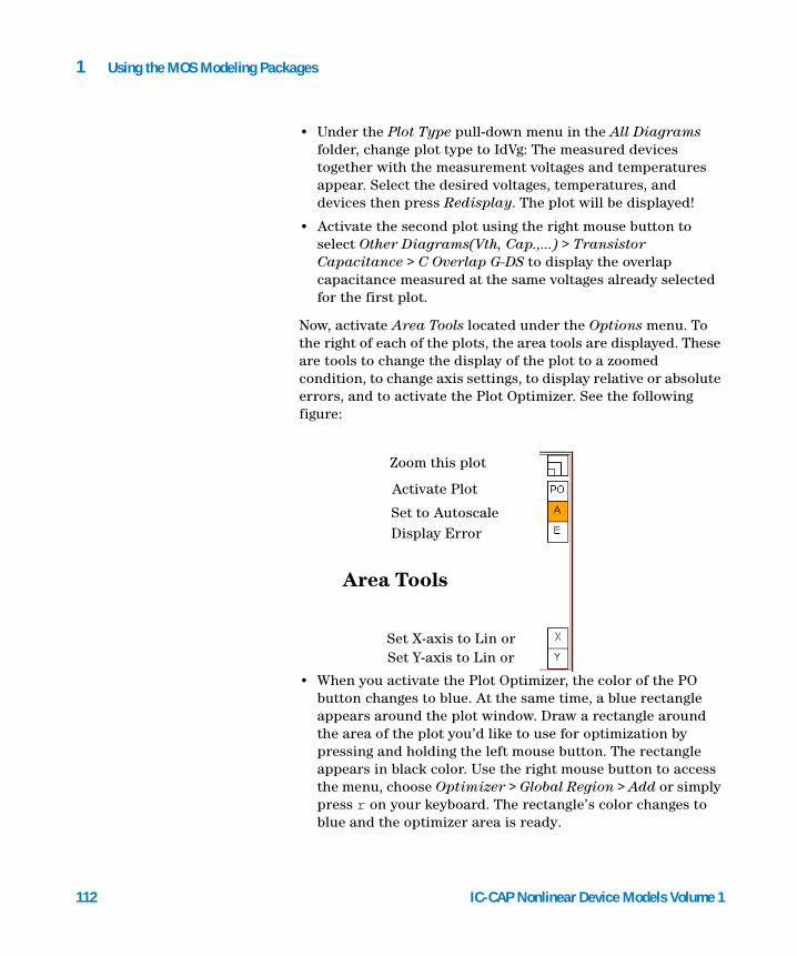
112
1 Using the MOS Modeling Packages
• Under the Plot Type pull-down menu in the All Diagrams folder, change plot type to IdVg: The measured devices together with the measurement voltages and temperatures appear. Select the desired voltages, temperatures, and devices then press Redisplay. The plot will be displayed!
• Activate the second plot using the right mouse button to select Other Diagrams(Vth, Cap.,...) > Transistor Capacitance > C Overlap G-DS to display the overlap capacitance measured at the same voltages already selected for the first plot.
Now, activate Area Tools located under the Options menu. To the right of each of the plots, the area tools are displayed. These are tools to change the display of the plot to a zoomed condition, to change axis settings, to display relative or absolute errors, and to activate the Plot Optimizer. See the following figure:
• When you activate the Plot Optimizer, the color of the PO button changes to blue. At the same time, a blue rectangle appears around the plot window. Draw a rectangle around the area of the plot you’d like to use for optimization by pressing and holding the left mouse button. The rectangle appears in black color. Use the right mouse button to access the menu, choose Optimizer > Global Region > Add or simply press r on your keyboard. The rectangle’s color changes to blue and the optimizer area is ready.
Zoom this plot
Activate Plot
Set to AutoscaleDisplay Error
Set X-axis to Lin or Set Y-axis to Lin or
Area Tools
IC-CAP Nonlinear Device Models Volume 1
Using the MOS Modeling Packages 1
IC-CAP Nonlinear Device Models Vo
• Select the appropriate area inside the second plot the same way. If the optimizer area in both plots appear with a blue rectangle, the plot optimizer is ready for use.
• Open the Plot Optimizer window by choosing Optimize > Open Optimizer from the menu or simply press o on your keyboard. The optimizer window opens.
• Inside the Plot Optimizer, select the parameters for use with this optimizing step. In our example, this would be VTH0.
• Save the configuration by clicking Save in the Plot Optimizer region at the top of the Data Display window (not the Optimizer window!) and enter a name for this configuration.
• Now, you can close the Data Display window and go to the Extract folder inside the BSIM4/PSP-GUI.
• Press Extract > Extraction Flow > Add, choose to add the Finetuning Extraction step. This step will be inserted into the extraction flow. If you click on this finetuning extraction, the optimizing routine you just defined is available under the Available Functions list to the right of the Extract window and is ready to use.
The Options menu enables you to add the calculated errors to the plot window, to set trace colors, or exchange the background color.
DC HTML
The folder HTML is used to generate a report file in HTML format. You can define a headline and comments for the report, specify the path to save the report, as well as the command to start the browser. You can also define the size of plots and the diagram background as it appears in the HTML report.
NOTE Generate HTML uses the project mps file (project_name~bsim*_dc_cv_extract.mps), not the loaded or imported one.
lume 1 113

114
1 Using the MOS Modeling Packages
If you use a path where an HTML project report already exists, you will get a warning. If the path doesn’t exist, you will be a prompted to accept creation of the specified directory.
The following figures show part of a generated HTML report. This report could be published over the intranet for use inside your company or over the web for customer use.
IC-CAP Nonlinear Device Models Volume 1

Using the MOS Modeling Packages 1
IC-CAP Nonlinear Device Models Volume 1 115
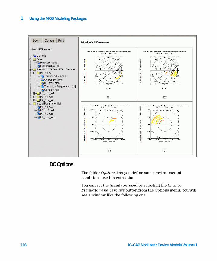
1 Using the MOS Modeling Packages
DC Options
116
The folder Options lets you define some environmental conditions used in extraction.
You can set the Simulator used by selecting the Change Simulator and Circuits button from the Options menu. You will see a window like the following one:
IC-CAP Nonlinear Device Models Volume 1
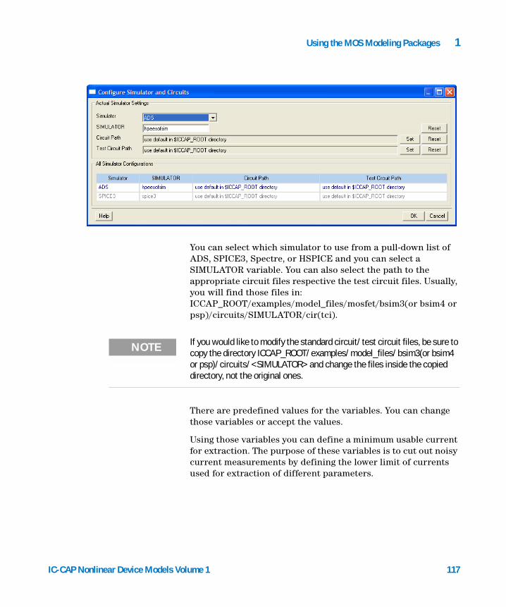
Using the MOS Modeling Packages 1
IC-CAP Nonlinear Device Models Vo
You can select which simulator to use from a pull-down list of ADS, SPICE3, Spectre, or HSPICE and you can select a SIMULATOR variable. You can also select the path to the appropriate circuit files respective the test circuit files. Usually, you will find those files in: ICCAP_ROOT/examples/model_files/mosfet/bsim3(or bsim4 or psp)/circuits/SIMULATOR/cir(tci).
NOTE If you would like to modify the standard circuit/test circuit files, be sure to copy the directory ICCAP_ROOT/examples/model_files/bsim3(or bsim4 or psp)/circuits/<SIMULATOR> and change the files inside the copied directory, not the original ones.
There are predefined values for the variables. You can change those variables or accept the values.
Using those variables you can define a minimum usable current for extraction. The purpose of these variables is to cut out noisy current measurements by defining the lower limit of currents used for extraction of different parameters.
lume 1 117
1 Using the MOS Modeling Packages
DC Boundaries
118
The folder Boundaries is intended to set optimizer boundaries for some parameters. Since the parameters differ between BSIM3 and BSIM4/PSP, there are little differences in the look of the boundaries folders.
IC-CAP Nonlinear Device Models Volume 1
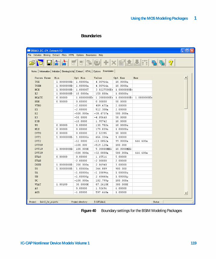
Using the MOS Modeling Packages 1
IC-CAP Nonlinear Device Models Vo
Boundaries
Figure 40 Boundary settings for the BSIM Modeling Packages
lume 1 119
120
1 Using the MOS Modeling Packages
On the left side, you can see the parameters to be optimized. The following columns display the minimum for the named parameter (the parameter’s reasonable physical minimum), an optimizer minimum and maximum column, followed by the parameter’s maximum, if a reasonable one exists. The white fields let you enter optimizer settings fitting your process needs. You can Save these settings for future extractions using the File menu. You can restore boundaries by clicking Boundaries > Set to Default from the menu.
The parameters and min/max values are taken from the IC-CAP Model Parameters folder.
IC-CAP Nonlinear Device Models Volume 1

Using the MOS Modeling Packages 1
Extraction of Parameters for the RF Models
IC-CAP Nonlinear Device Models Vo
Start extraction of RF parameters for the BSIM3 or BSIM4/PSP models by clicking the appropriate extract model to open the graphic user interface (GUI) you are already familiar with. The tasks are separated on subfolders for easy handling. Some of the folders are using the same look as in the DC Extraction part of the BSIM3 and BSIM4/PSP Modeling Tools.
The top row menus are described in “DC and CV Measurement of MOSFET’s for the MOS Models” on page 23.
As soon as you click File > Open, the PreSelection dialog box opens, prompting you for some basic definitions for parameter extraction.
lume 1 121
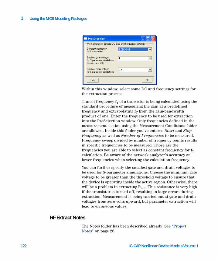
122
1 Using the MOS Modeling Packages
Within this window, select some DC and frequency settings for the extraction process.
Transit frequency fT of a transistor is being calculated using the standard procedure of measuring the gain at a predefined frequency and extrapolating fT from the gain-bandwidth product of one. Enter the frequency to be used for extraction into the PreSelection window. Only frequencies defined in the measurement section using the Measurement Conditions folder are allowed. Inside this folder you’ve entered Start and Stop Frequency as well as Number of Frequencies to be measured. Frequency sweep divided by number of frequency points results in specific frequencies to be measured. Those are the frequencies you are able to select as constant frequency for fT calculation. Be aware of the network analyzer’s accuracy at lower frequencies when selecting the calculation frequency.
You can further specify the smallest gate and drain voltages to be used for S-parameter simulations. Choose the minimum gate voltage to be greater than the threshold voltage to ensure that the device is operating inside the active region. Otherwise, there will be a problem in extracting Rout. This resistance is very high if the transistor is turned off, resulting in large errors during extraction. Measurement is being carried out at gate and drain voltages from zero volts upward, but parameter extraction will lead to erroneous values.
RF Extract Notes
The Notes folder has been described already. See “Project Notes” on page 26.
IC-CAP Nonlinear Device Models Volume 1
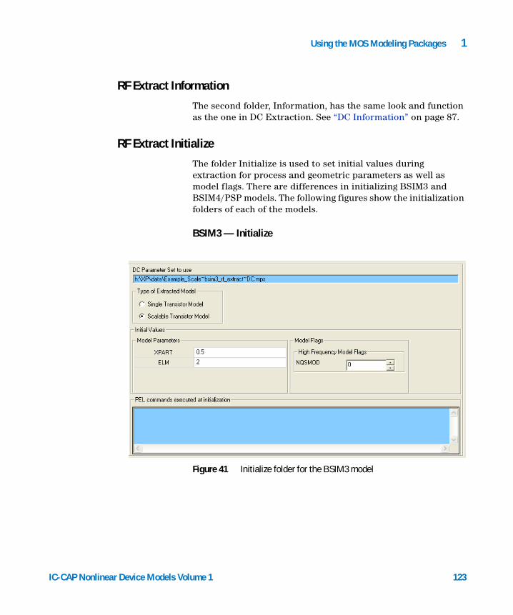
Using the MOS Modeling Packages 1
RF Extract Information
IC-CAP Nonlinear Device Models Vo
The second folder, Information, has the same look and function as the one in DC Extraction. See “DC Information” on page 87.
RF Extract Initialize
The folder Initialize is used to set initial values during extraction for process and geometric parameters as well as model flags. There are differences in initializing BSIM3 and BSIM4/PSP models. The following figures show the initialization folders of each of the models.
BSIM3 — Initialize
Figure 41 Initialize folder for the BSIM3 model
lume 1 123
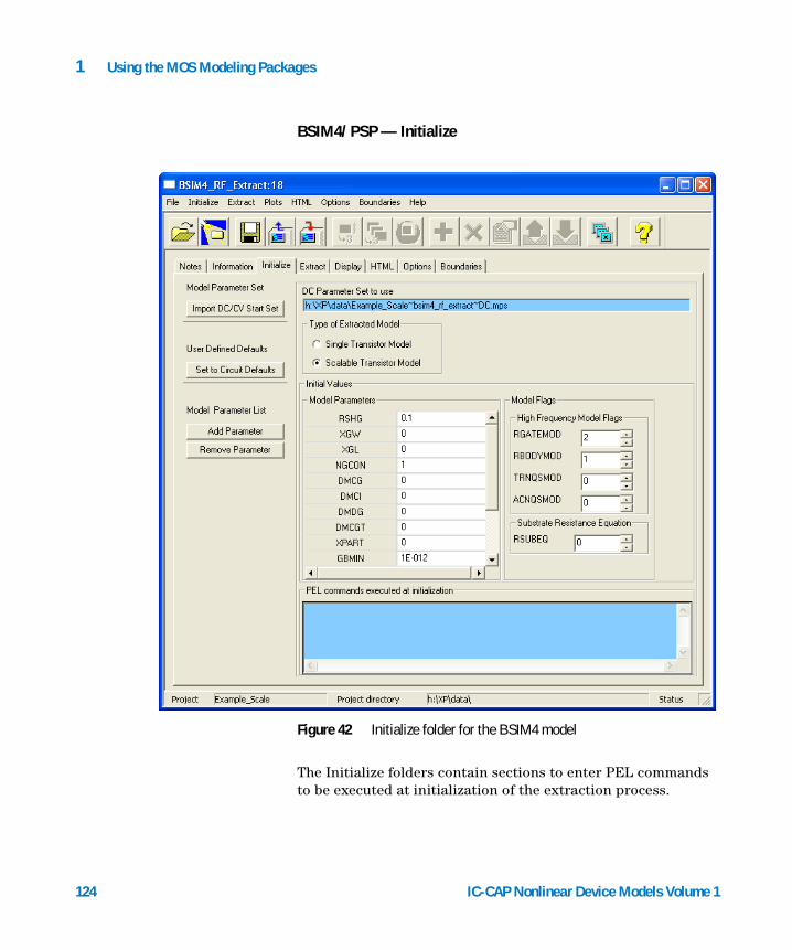
124
1 Using the MOS Modeling Packages
BSIM4/PSP — Initialize
The Initialize folders contain sections to enter PEL commands to be executed at initialization of the extraction process.
Figure 42 Initialize folder for the BSIM4 model
IC-CAP Nonlinear Device Models Volume 1
Using the MOS Modeling Packages 1
Model Parameter Sets
IC-CAP Nonlinear Device Models Vo
From the Initialize menu, you can Import DC/CV Start Set to be used for RF extraction. You get a list of existing *.mps files for selection. A selected *.mps file will be copied into the RF project directory. This action will set parameter values extracted from DC/CV measurements as starting points for RF extraction. Since the devices measured for RF extraction are very compact multifinger transistors due to design requirements (and also to enhance accuracy through reducing measurement noise during network analyzer measurements), their parameters differ from the ones extracted from DC measurements. To get results consistent for the process—not only for the actual measured device—the extraction of RF relevant parameters must start with initial parameter start points to fit the S-parameters at low frequencies. Therefore, using parameters extracted during the DC extraction process are used to give start points of good accuracy for the RF extraction process.
The path and filename of the selected start set will be shown on blue background.
NOTE You cannot change directly the path and filename of the start set in the field DC Parameter Set to use. Instead, use the Import DC/CV Start Set button from the menu to enter the correct path or to browse for the location of your start set.
Set parameters to circuit default values: Choosing the Set to Circuit Default Values menu item restores the defaults.
You can Add or Remove Parameters from the Initial Values list in the middle of the Initialize folder using the Initialize menu.
Select the type of model to be extracted. There are two selections possible: Single or Scalable Transistor Model. For a detailed explanation, see “Single Transistor Model” on page 282 or “Fully Scalable Device” on page 283.
You can set initial parameter values manually. To do so, enter the desired values into the parameter fields provided for several parameters.
lume 1 125
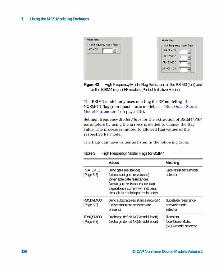
126
1 Using the MOS Modeling Packages
The BSIM3 model only uses one flag for RF modeling—the NQSMOD flag (non-quasi-static model, see “Non-Quasi-Static Model Parameters” on page 419).
Set high frequency Model Flags for the extraction of BSIM4/PSP parameters by using the arrows provided to change the flag value. The process is limited to allowed flag values of the respective RF model.
The flags can have values as listed in the following table.
Figure 43 High Frequency Model Flag Selection for the BSIM3 (left) and for the BSIM4 (right) RF models (Part of Initialize Folder)
Table 3 High Frequency Model Flags for BSIM4
Values Meaning
RGATEMOD[Page 8-8]
0 (no gate resistance)1 (constant gate resistance)2 (variable gate resistance)3 (two gate resistances, overlap capacitance current will not pass through intrinsic input resistance)
Gate resistance model selector
RBODYMOD[Page 8-9]
0 (no substrate resistance network)1 (five substrate resistors are present)
Substrate resistance network model selector
TRNQSMOD[Page 8-3]
0 (charge deficit NQS model is off)1 (charge deficit NQS model is on)
Transient Non-Quasi-Static (NQS) model selector
IC-CAP Nonlinear Device Models Volume 1
Using the MOS Modeling Packages 1
IC-CAP Nonlinear Device Models Vo
ACNQSMOD[Page 8-5]
0 (small signal AC charge deficit NQS model is off)1 (small signal AC charge deficit NQS model is on)
AC small-signal Non-Quasi-Static model selector
Note [Page 8-X] refers to the page numbers of the BSIM4.3.0 Manual from UC Berkeley [1]
Table 3 High Frequency Model Flags for BSIM4 (continued)
Values Meaning
RF Extract
Within this folder, you define the extraction process for the parameters of the devices. There is a standard extraction flow implemented, but you can change this flow if you find another one suits your needs better than the default flow.
lume 1 127
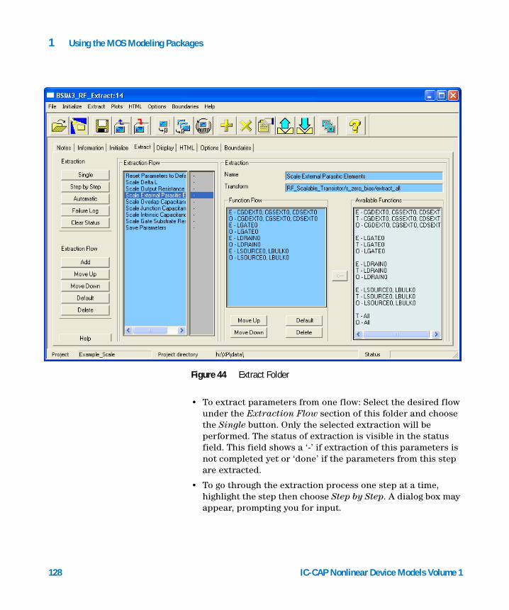
128
1 Using the MOS Modeling Packages
• To extract parameters from one flow: Select the desired flow under the Extraction Flow section of this folder and choose the Single button. Only the selected extraction will be performed. The status of extraction is visible in the status field. This field shows a ‘-’ if extraction of this parameters is not completed yet or ‘done’ if the parameters from this step are extracted.
• To go through the extraction process one step at a time, highlight the step then choose Step by Step. A dialog box may appear, prompting you for input.
Figure 44 Extract Folder
IC-CAP Nonlinear Device Models Volume 1

Using the MOS Modeling Packages 1
IC-CAP Nonlinear Device Models Vo
• To automatically extract all parameters using the extraction flows listed under the Extraction Flow section: Choose Automatic. The programmed extraction flow will be extracting all parameters defined in the active extraction flow.
• All warnings and errors during the extraction process are written to the failure log, which is opened using the Failure Log button.
If you would like to clear the status of extraction, use Clear Status.
NOTE Already extracted parameters are reset to defaults!
• You can add steps to the extraction flow by clicking the Add button on the left side of the folder under the section Extraction Flow. You will be prompted for an extraction to add. Select the desired extraction and choose Add on the Add Extraction folder.
• Change the flow of extraction by using the Move Up or Move Down buttons to move a selected extraction routine one step up or down.
• The Default button restores the order of parameter extraction as it was in the beginning of a project.
• To delete a step: Choose the Delete button.
NOTE You cannot delete the first (Reset Parameters) and the last (Save Parameters) step inside an extraction flow.
• To export the extracted parameters: The step Save Parameters inside the Extraction Flow informs you of the path and name for the saved .mps or .lib file.
On the right side of the Extract folder, you will find a field named Extraction.
lume 1 129
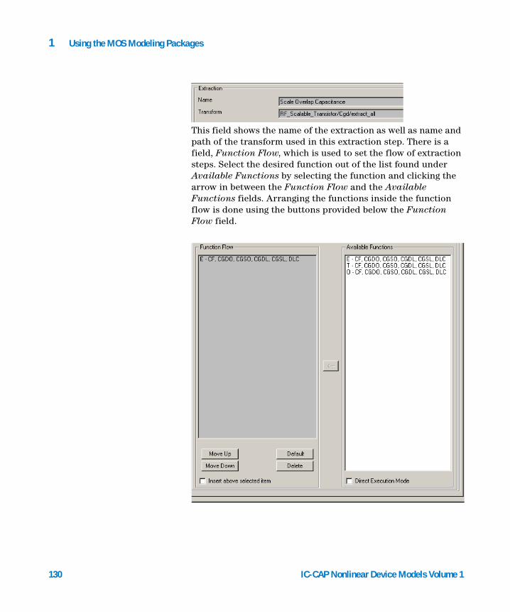
130
1 Using the MOS Modeling Packages
This field shows the name of the extraction as well as name and path of the transform used in this extraction step. There is a field, Function Flow, which is used to set the flow of extraction steps. Select the desired function out of the list found under Available Functions by selecting the function and clicking the arrow in between the Function Flow and the Available Functions fields. Arranging the functions inside the function flow is done using the buttons provided below the Function Flow field.
IC-CAP Nonlinear Device Models Volume 1
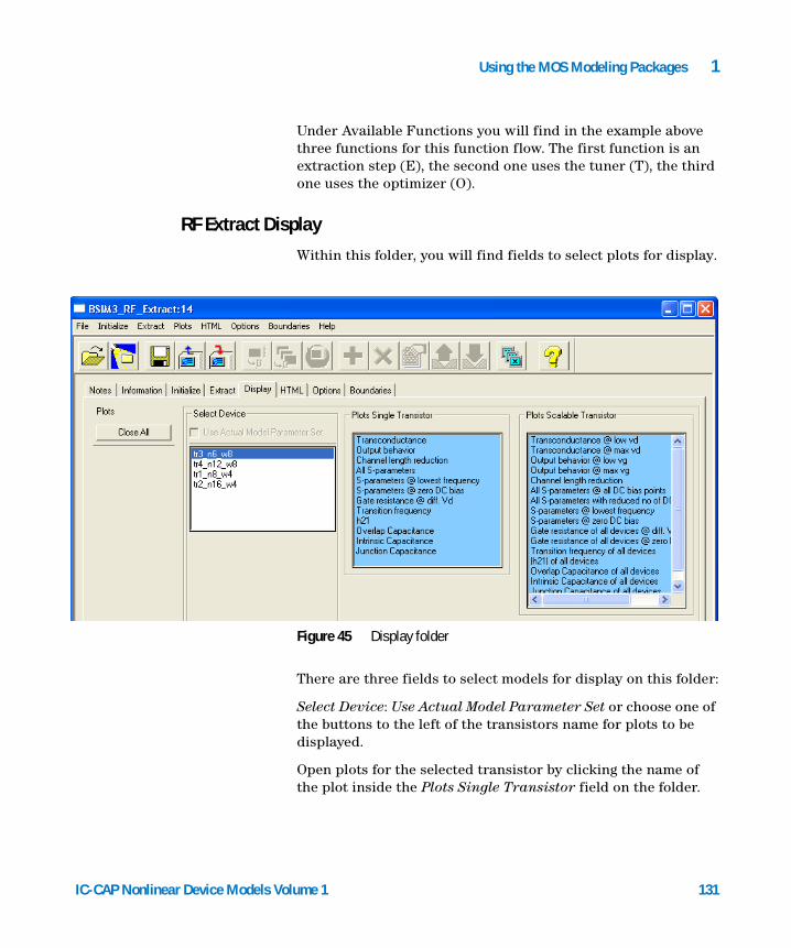
Using the MOS Modeling Packages 1
IC-CAP Nonlinear Device Models Vo
Under Available Functions you will find in the example above three functions for this function flow. The first function is an extraction step (E), the second one uses the tuner (T), the third one uses the optimizer (O).
RF Extract Display
Within this folder, you will find fields to select plots for display.
There are three fields to select models for display on this folder:
Select Device: Use Actual Model Parameter Set or choose one of the buttons to the left of the transistors name for plots to be displayed.
Open plots for the selected transistor by clicking the name of the plot inside the Plots Single Transistor field on the folder.
Figure 45 Display folder
lume 1 131
132
1 Using the MOS Modeling Packages
Open plots for scalable transistor models by clicking the name of the desired plots inside the Plots Scalable Transistor field on this folder.
NOTE You can only choose a plot for the extracted model that was selected in the field Type of Extracted Model on the Initialize folder. Plots inside the other fields are not selectable.
Each plot is opened in a new window. Close all windows by using the Close All button on the right side of the Display folder or close single windows using the Close icon inside the appropriate window.
RF Extract HTML
This folder helps you to prepare a report file in HTML format to be displayed using an internet browser.
Since this folder is the same as in the DC Extraction section, see “DC HTML” on page 113 for details.
RF Extract Options
This folder is used to set variables for the extraction process and options for plots to be displayed.
IC-CAP Nonlinear Device Models Volume 1
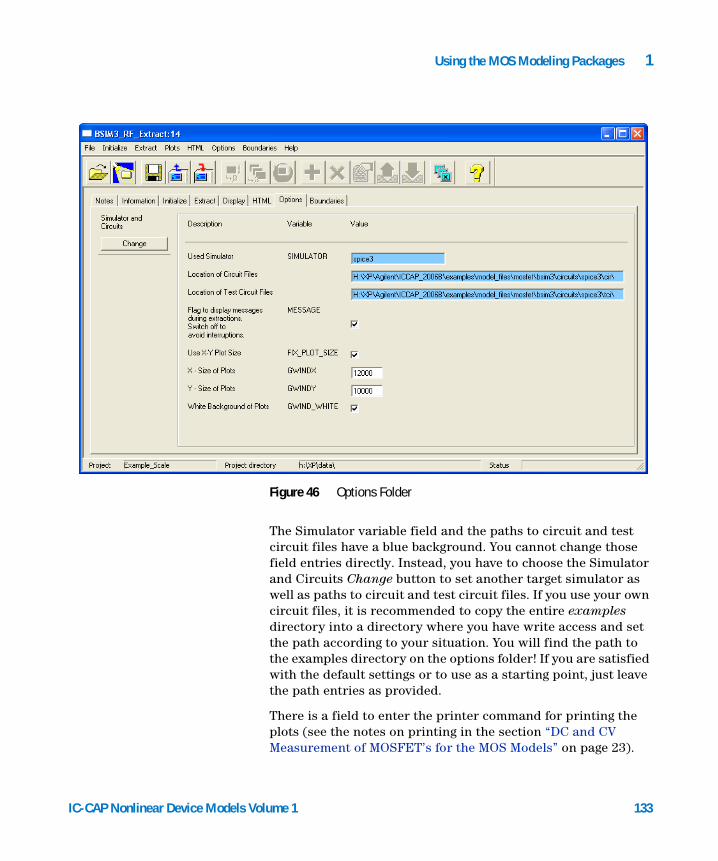
Using the MOS Modeling Packages 1
IC-CAP Nonlinear Device Models Vo
The Simulator variable field and the paths to circuit and test circuit files have a blue background. You cannot change those field entries directly. Instead, you have to choose the Simulator and Circuits Change button to set another target simulator as well as paths to circuit and test circuit files. If you use your own circuit files, it is recommended to copy the entire examples directory into a directory where you have write access and set the path according to your situation. You will find the path to the examples directory on the options folder! If you are satisfied with the default settings or to use as a starting point, just leave the path entries as provided.
There is a field to enter the printer command for printing the plots (see the notes on printing in the section “DC and CV Measurement of MOSFET’s for the MOS Models” on page 23).
Figure 46 Options Folder
lume 1 133
134
1 Using the MOS Modeling Packages
If you want to change the plot window size, choose Use X-Y Plot Size: Fixed_Plot_Size and enter the desired X and Y size into the respective fields. You are able to change the background color of the plot window from black to white by activating the field: White background of plots.
Circuit Files
The circuit files are located in:ICCAP_ROOT/example/model_files/mosfet/bsim3(or bsim4 or psp)/circuits
You will find subdirectories below the circuits directory for each supported simulator (hpeesofsim, hspice, spectre, spice3). Each directory contains a circuit (cir) as well as a test circuit (tci) directory, which contain the circuit files using the appropriate simulator syntax.
RF Extract Boundaries
The Boundaries folder is the same as the one in DC Extraction. For details, see “DC Boundaries” on page 118.
IC-CAP Nonlinear Device Models Volume 1

Agilent 85190A IC-CAP 2008
2HiSIM2 and HiSIM_HV Characterization
Modeled Device Characteristics of the HiSIM2 model 137
SPICE Model Parameters 139
RF Circuit used for HiSIM2 153
HiSIM_HV model 157
Additional SPICE Model Parameters for HiSIM_HV 162
References 164
This chapter describes the measurement and extraction of parameters for the HiSIM2 and the HiSIM_HV models, developed by AdMOS.
You will find the HISIM2 model in the first parts of this chapter, an additional part is dedicated to the HISIM high voltage model. Since this model is based on the HISIM2 model, the HV part of this chapter describes only the differences between those models. The high voltage model uses some additional parameters not present in HISIM2.
The Modeling Packages all use similar Graphic User Interfaces (GUI). Performing the measurement and extraction tasks using one of the Modeling Packages is similar and therefore only needs to be described once. See Chapter 1, “Using the MOS Modeling Packages.”
HiSIM is a complete Surface-Potential-Based model to simulate new generation MOSFETs, developed by Hiroshima University. The web address listed in “References” #1 points to the web site of the HiSIM research center.
135Agilent Technologies
136
2 HiSIM2 and HiSIM_HV Characterization
This short documentation lists the effects of modern MOSFETs using 45nm-technology or smaller, and the SPICE parameters used. It is based on HiSIM 2.4.0, released March, 2007 respective on HiSIM_HV, released June, 2008.
HiSIM2
HiSIM2 and HiSIM_HV Characterization 2
Modeled Device Characteristics of the HiSIM2 model
HiSIM2
In HISIM 2.4.0, the following device characteristics are included (see “References” #2):
• Drain Current IDS
• Short Channel Effect
• Reverse Short Channel Effect: impurity pile-up and pocket implant
• Mobility Models:
• Universal
• High Field
• Quantum-Mechanical Effect
• Gate-Poly Depletion Effect
• Channel Length Modulation
• Narrow Channel Effect
• Temperature Dependency:
• Thermal Voltage
• Band Gap
• ni
• Phonon Scattering
• Maximum Velocity
• Pinch-Off
• Shallow Trench Isolation:
• Threshold Voltage
• Mobility
• Leakage Current
• Leakage Currents Modeled:
• IBS
• IGate
• IGIDL
137
138
2 HiSIM2 and HiSIM_HV Characterization
• Capacitances
• Intrinsic
• Overlap
• Lateral-Field-Induced
• Fringing
• Junction Diodes:
• Current
• Capacitances
• Higher Order Phenomena
• Harmonic Distortion
• Noise Characteristics:
• 1/f
• Thermal
• Induced Gate
• GIDL
• Small-Signal Analysis
• Large-Signal Analysis
• Source/Drain Resistances
HiSIM2
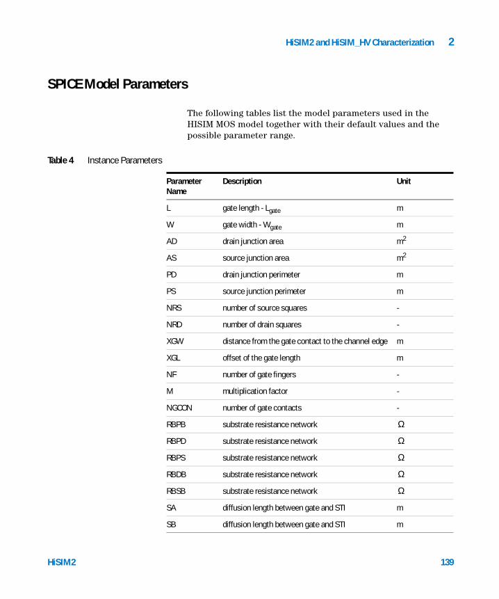
HiSIM2 and HiSIM_HV Characterization 2
SPICE Model Parameters
HiSIM2
The following tables list the model parameters used in the HISIM MOS model together with their default values and the possible parameter range.
Table 4 Instance Parameters
Parameter Name
Description Unit
L gate length - Lgate m
W gate width - Wgate m
AD drain junction area m2
AS source junction area m2
PD drain junction perimeter m
PS source junction perimeter m
NRS number of source squares -
NRD number of drain squares -
XGW distance from the gate contact to the channel edge m
XGL offset of the gate length m
NF number of gate fingers -
M multiplication factor -
NGCON number of gate contacts -
RBPB substrate resistance network
RBPD substrate resistance network
RBPS substrate resistance network
RBDB substrate resistance network
RBSB substrate resistance network
SA diffusion length between gate and STI m
SB diffusion length between gate and STI m
Ω
Ω
Ω
Ω
Ω
139
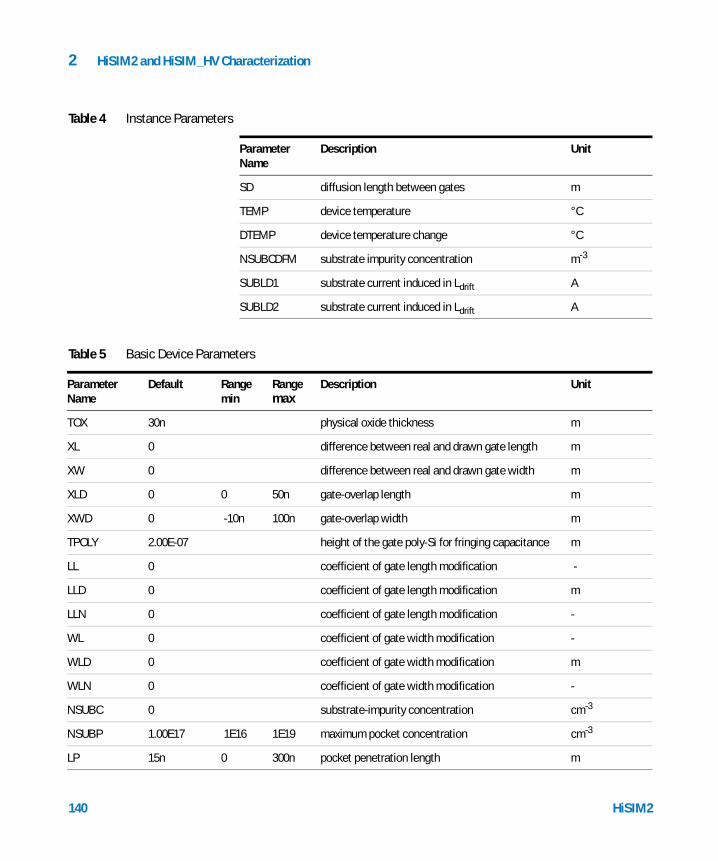
2 HiSIM2 and HiSIM_HV Characterization
SD diffusion length between gates m
TEMP device temperature °C
DTEMP device temperature change °C
NSUBCDFM substrate impurity concentration m-3
SUBLD1 substrate current induced in Ldrift A
SUBLD2 substrate current induced in Ldrift A
Table 5 Basic Device Parameters
Parameter Name
Default Rangemin
Rangemax
Description Unit
TOX 30n physical oxide thickness m
XL 0 difference between real and drawn gate length m
XW 0 difference between real and drawn gate width m
XLD 0 0 50n gate-overlap length m
XWD 0 -10n 100n gate-overlap width m
TPOLY 2.00E-07 height of the gate poly-Si for fringing capacitance m
LL 0 coefficient of gate length modification -
LLD 0 coefficient of gate length modification m
LLN 0 coefficient of gate length modification -
WL 0 coefficient of gate width modification -
WLD 0 coefficient of gate width modification m
WLN 0 coefficient of gate width modification -
NSUBC 0 substrate-impurity concentration cm-3
NSUBP 1.00E17 1E16 1E19 maximum pocket concentration cm-3
LP 15n 0 300n pocket penetration length m
Table 4 Instance Parameters
Parameter Name
Description Unit
140 HiSIM2
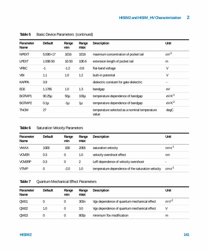
HiSIM2 and HiSIM_HV Characterization 2
NPEXT 5.00E+17 1E16 1E18 maximum concentration of pocket tail cm-3
LPEXT 1.00E-50 1E-50 10E-6 extension length of pocket tail m
VFBC -1 -1.2 -0.8 flat-band voltage V
VBI 1.1 1.0 1.2 built-in potential V
KAPPA 3.9 dielectric constant for gate dielectric -
EG0 1.1785 1.0 1.3 bandgap eV
BGTMP1 90.25µ 50µ 100µ temperature dependence of bandgap eV·K-1
BGTMP2 0.1µ -1µ 1µ temperature dependence of bandgap eV·K-2
TNOM 27 temperature selected as a nominal temperature value
degC
Table 6 Saturation Velocity Parameters
Parameter Name
Default Rangemin
Rangemax
Description Unit
VMAX 10E6 1E6 20E6 saturation velocity cm·s-1
VOVER 0.3 0 1.0 velocity overshoot effect cm
VOVERP 0.3 0 2 Leff dependence of velocity overshoot -
VTMP 0 -2.0 1.0 temperature dependence of the saturation velocity cm·s-1
Table 7 Quantum Mechanical Effect Parameters
Parameter Name
Default Rangemin
Rangemax
Description Unit
QME1 0 0 300n Vgs dependence of quantum mechanical effect m·V-2
QME2 1.0 0 3.0 Vgs dependence of quantum mechanical effect V
QME3 0 0 800p minimum Tox modification m
Table 5 Basic Device Parameters (continued)
Parameter Name
Default Rangemin
Rangemax
Description Unit
HiSIM2 141
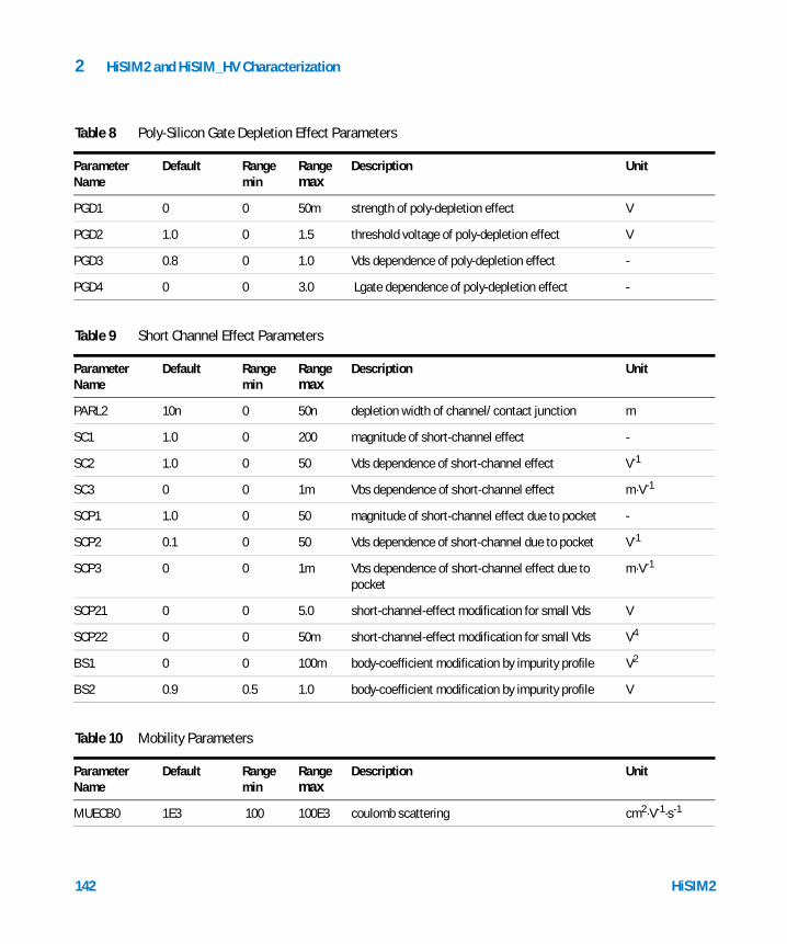
2 HiSIM2 and HiSIM_HV Characterization
Table 8 Poly-Silicon Gate Depletion Effect Parameters
Parameter Name
Default Rangemin
Rangemax
Description Unit
PGD1 0 0 50m strength of poly-depletion effect V
PGD2 1.0 0 1.5 threshold voltage of poly-depletion effect V
PGD3 0.8 0 1.0 Vds dependence of poly-depletion effect -
PGD4 0 0 3.0 Lgate dependence of poly-depletion effect -
Table 9 Short Channel Effect Parameters
Parameter Name
Default Rangemin
Rangemax
Description Unit
PARL2 10n 0 50n depletion width of channel/contact junction m
SC1 1.0 0 200 magnitude of short-channel effect -
SC2 1.0 0 50 Vds dependence of short-channel effect V-1
SC3 0 0 1m Vbs dependence of short-channel effect m·V-1
SCP1 1.0 0 50 magnitude of short-channel effect due to pocket -
SCP2 0.1 0 50 Vds dependence of short-channel due to pocket V-1
SCP3 0 0 1m Vbs dependence of short-channel effect due to pocket
m·V-1
SCP21 0 0 5.0 short-channel-effect modification for small Vds V
SCP22 0 0 50m short-channel-effect modification for small Vds V4
BS1 0 0 100m body-coefficient modification by impurity profile V2
BS2 0.9 0.5 1.0 body-coefficient modification by impurity profile V
Table 10 Mobility Parameters
Parameter Name
Default Rangemin
Rangemax
Description Unit
MUECB0 1E3 100 100E3 coulomb scattering cm2·V-1·s-1
142 HiSIM2
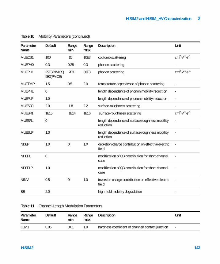
HiSIM2 and HiSIM_HV Characterization 2
MUECB1 100 15 10E3 coulomb scattering cm2·V-1·s-1
MUEPH0 0.3 0.25 0.3 phonon scattering -
MUEPH1 25E3(NMOS)9E3(PMOS)
2E3 30E3 phonon scattering cm2·V-1·s-1
MUETMP 1.5 0.5 2.0 temperature dependence of phonon scattering -
MUEPHL 0 length dependence of phonon mobility reduction -
MUEPLP 1.0 length dependence of phonon mobility reduction -
MUESR0 2.0 1.8 2.2 surface-roughness scattering -
MUESR1 1E15 1E14 1E16 surface-roughness scattering cm2·V-1·s-1
MUESRL 0 length dependence of surface roughness mobility reduction
-
MUESLP 1.0 length dependence of surface roughness mobility reduction
-
NDEP 1.0 0 1.0 depletion charge contribution on effective-electric field
-
NDEPL 0 modification of QB contribution for short-channel case
-
NDEPLP 1.0 modification of QB contribution for short-channel case
-
NINV 0.5 0 1.0 inversion charge contribution on effective-electric field
-
BB 2.0 high-field-mobility degradation -
Table 11 Channel-Length Modulation Parameters
Parameter Name
Default Rangemin
Rangemax
Description Unit
CLM1 0.05 0.01 1.0 hardness coefficient of channel/contact junction -
Table 10 Mobility Parameters (continued)
Parameter Name
Default Rangemin
Rangemax
Description Unit
HiSIM2 143
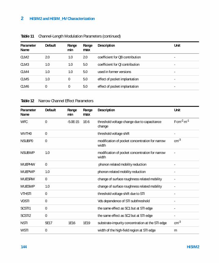
2 HiSIM2 and HiSIM_HV Characterization
CLM2 2.0 1.0 2.0 coefficient for QB contribution -
CLM3 1.0 1.0 5.0 coefficient for QI contribution -
CLM4 1.0 1.0 5.0 used in former versions -
CLM5 1.0 0 5.0 effect of pocket implantation -
CLM6 0 0 5.0 effect of pocket implantation -
Table 12 Narrow Channel Effect Parameters
Parameter Name
Default Rangemin
Rangemax
Description Unit
WFC 0 -5.0E-15 1E-6 threshold voltage change due to capacitance change
F·cm-2·m-1
WVTH0 0 threshold voltage shift -
NSUBP0 0 modification of pocket concentration for narrow width
cm-3
NSUBWP 1.0 modification of pocket concentration for narrow width
-
MUEPHW 0 phonon related mobility reduction -
MUEPWP 1.0 phonon related mobility reduction -
MUESRW 0 change of surface roughness related mobility -
MUESWP 1.0 change of surface roughness related mobility -
VTHSTI 0 threshold voltage shift due to STI -
VDSTI 0 Vds dependence of STI subthreshold -
SCSTI1 0 the same effect as SC1 but at STI edge -
SCSTI2 0 the same effect as SC2 but at STI edge -
NSTI 5E17 1E16 1E19 substrate-impurity concentration at the STI edge cm-3
WSTI 0 width of the high-field region at STI edge m
Table 11 Channel-Length Modulation Parameters (continued)
Parameter Name
Default Rangemin
Rangemax
Description Unit
144 HiSIM2
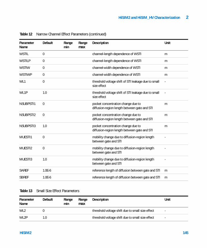
HiSIM2 and HiSIM_HV Characterization 2
WSTIL 0 channel-length dependence of WSTI m
WSTILP 0 channel-length dependence of WSTI m
WSTIW 0 channel-width dependence of WSTI m
WSTIWP 0 channel-width dependence of WSTI m
WL1 0 threshold voltage shift of STI leakage due to small size effect
-
WL1P 1.0 threshold voltage shift of STI leakage due to small size effect
-
NSUBPSTI1 0 pocket concentration change due to diffusion-region length between gate and STI
m
NSUBPSTI2 0 pocket concentration change due to diffusion-region length between gate and STI
m
NSUBPSTI3 1.0 pocket concentration change due to diffusion-region length between gate and STI
m
MUESTI1 0 mobility change due to diffusion-region length between gate and STI
-
MUESTI2 0 mobility change due to diffusion-region length between gate and STI
-
MUESTI3 1.0 mobility change due to diffusion-region length between gate and STI
-
SAREF 1.0E-6 reference length of diffusion between gate and STI m
SBREF 1.0E-6 reference length of diffusion between gate and STI m
Table 13 Small Size Effect Parameters
Parameter Name
Default Rangemin
Rangemax
Description Unit
WL2 0 threshold voltage shift due to small size effect -
WL2P 1.0 threshold voltage shift due to small size effect -
Table 12 Narrow Channel Effect Parameters (continued)
Parameter Name
Default Rangemin
Rangemax
Description Unit
HiSIM2 145
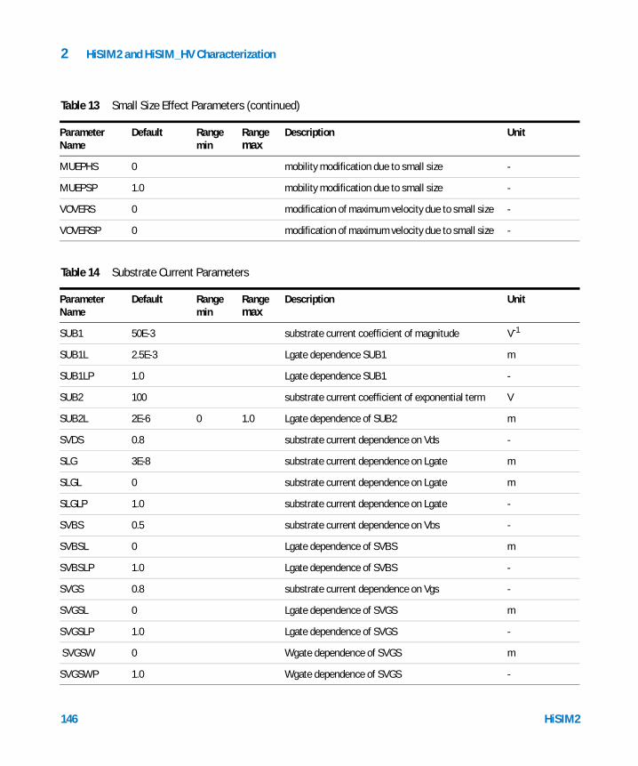
2 HiSIM2 and HiSIM_HV Characterization
MUEPHS 0 mobility modification due to small size -
MUEPSP 1.0 mobility modification due to small size -
VOVERS 0 modification of maximum velocity due to small size -
VOVERSP 0 modification of maximum velocity due to small size -
Table 14 Substrate Current Parameters
Parameter Name
Default Rangemin
Rangemax
Description Unit
SUB1 50E-3 substrate current coefficient of magnitude V-1
SUB1L 2.5E-3 Lgate dependence SUB1 m
SUB1LP 1.0 Lgate dependence SUB1 -
SUB2 100 substrate current coefficient of exponential term V
SUB2L 2E-6 0 1.0 Lgate dependence of SUB2 m
SVDS 0.8 substrate current dependence on Vds -
SLG 3E-8 substrate current dependence on Lgate m
SLGL 0 substrate current dependence on Lgate m
SLGLP 1.0 substrate current dependence on Lgate -
SVBS 0.5 substrate current dependence on Vbs -
SVBSL 0 Lgate dependence of SVBS m
SVBSLP 1.0 Lgate dependence of SVBS -
SVGS 0.8 substrate current dependence on Vgs -
SVGSL 0 Lgate dependence of SVGS m
SVGSLP 1.0 Lgate dependence of SVGS -
SVGSW 0 Wgate dependence of SVGS m
SVGSWP 1.0 Wgate dependence of SVGS -
Table 13 Small Size Effect Parameters (continued)
Parameter Name
Default Rangemin
Rangemax
Description Unit
146 HiSIM2
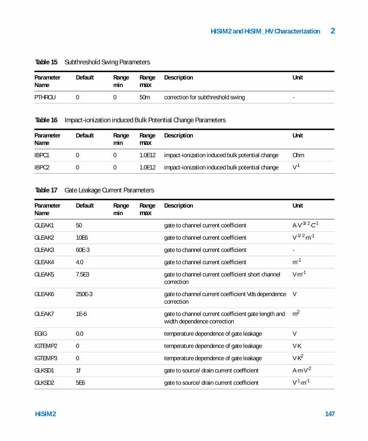
HiSIM2 and HiSIM_HV Characterization 2
Table 15 Subthreshold Swing Parameters
Parameter Name
Default Rangemin
Rangemax
Description Unit
PTHROU 0 0 50m correction for subthreshold swing -
Table 16 Impact-ionization induced Bulk Potential Change Parameters
Parameter Name
Default Rangemin
Rangemax
Description Unit
IBPC1 0 0 1.0E12 impact-ionization induced bulk potential change Ohm
IBPC2 0 0 1.0E12 impact-ionization induced bulk potential change V-1
Table 17 Gate Leakage Current Parameters
Parameter Name
Default Rangemin
Rangemax
Description Unit
GLEAK1 50 gate to channel current coefficient A·V-3/2·C-1
GLEAK2 10E6 gate to channel current coefficient V-1/2·m-1
GLEAK3 60E-3 gate to channel current coefficient -
GLEAK4 4.0 gate to channel current coefficient m-1
GLEAK5 7.5E3 gate to channel current coefficient short channel correction
V·m-1
GLEAK6 250E-3 gate to channel current coefficient Vds dependence correction
V
GLEAK7 1E-6 gate to channel current coefficient gate length and width dependence correction
m2
EGIG 0.0 temperature dependence of gate leakage V
IGTEMP2 0 temperature dependence of gate leakage V·K
IGTEMP3 0 temperature dependence of gate leakage V·K2
GLKSD1 1f gate to source/drain current coefficient A·m·V-2
GLKSD2 5E6 gate to source/drain current coefficient V-1·m-1
HiSIM2 147
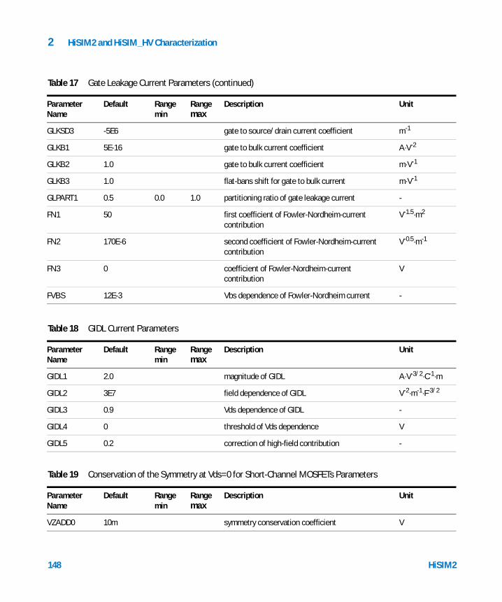
2 HiSIM2 and HiSIM_HV Characterization
GLKSD3 -5E6 gate to source/drain current coefficient m-1
GLKB1 5E-16 gate to bulk current coefficient A·V-2
GLKB2 1.0 gate to bulk current coefficient m·V-1
GLKB3 1.0 flat-bans shift for gate to bulk current m·V-1
GLPART1 0.5 0.0 1.0 partitioning ratio of gate leakage current -
FN1 50 first coefficient of Fowler-Nordheim-current contribution
V-1.5·m2
FN2 170E-6 second coefficient of Fowler-Nordheim-current contribution
V-0.5·m-1
FN3 0 coefficient of Fowler-Nordheim-current contribution
V
FVBS 12E-3 Vbs dependence of Fowler-Nordheim current -
Table 18 GIDL Current Parameters
Parameter Name
Default Rangemin
Rangemax
Description Unit
GIDL1 2.0 magnitude of GIDL A·V-3/2·C-1·m
GIDL2 3E7 field dependence of GIDL V-2·m-1·F-3/2
GIDL3 0.9 Vds dependence of GIDL -
GIDL4 0 threshold of Vds dependence V
GIDL5 0.2 correction of high-field contribution -
Table 19 Conservation of the Symmetry at Vds=0 for Short-Channel MOSFETs Parameters
Parameter Name
Default Rangemin
Rangemax
Description Unit
VZADD0 10m symmetry conservation coefficient V
Table 17 Gate Leakage Current Parameters (continued)
Parameter Name
Default Rangemin
Rangemax
Description Unit
148 HiSIM2
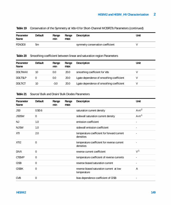
HiSIM2 and HiSIM_HV Characterization 2
PZADD0 5m symmetry conservation coefficient V
Table 20 Smoothing coefficient between linear and saturation region Parameters
Parameter Name
Default Rangemin
Rangemax
Description Unit
DDLTMAX 10 0.0 20.0 smoothing coefficient for Vds V
DDLTSLP 0 0.0 20.0 Lgate dependence of smoothing coefficient V
DDLTICT 10 -3.0 20.0 Lgate dependence of smoothing coefficient V
Table 21 Source/Bulk and Drain/Bulk Diodes Parameters
Parameter Name
Default Rangemin
Rangemax
Description Unit
JS0 0.5E-6 saturation current density A·m-2
JS0SW 0 sidewall saturation current density A·m-1
NJ 1.0 emission coefficient -
NJSW 1.0 sidewall emission coefficient -
XTI 2.0 temperature coefficient for forward current densities
-
XTI2 0 temperature coefficient for reverse current densities
-
DIVX 0 reverse current coefficient V-1
CTEMP 0 temperature coefficient of reverse currents -
CISB 0 reverse biased saturation current -
CISBK 0 reverse biased saturation current at low temperature
A
CVB 0 bias dependence coefficient of CISB -
Table 19 Conservation of the Symmetry at Vds=0 for Short-Channel MOSFETs Parameters (continued)
Parameter Name
Default Rangemin
Rangemax
Description Unit
HiSIM2 149
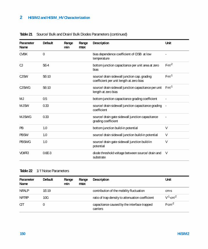
2 HiSIM2 and HiSIM_HV Characterization
CVBK 0 bias dependence coefficient of CISB at low temperature
-
CJ 5E-4 bottom junction capacitance per unit area at zero bias
F·m-2
CJSW 5E-10 source/drain sidewall junction cap. grading coefficient per unit length at zero bias
F·m-1
CJSWG 5E-10 source/drain sidewall junction capacitance per unit length at zero bias
F·m-1
MJ 0.5 bottom junction capacitance grading coefficient -
MJSW 0.33 source/drain sidewall junction capacitance grading coefficient
-
MJSWG 0.33 source/drain gate sidewall junction capacitance grading coefficient
-
PB 1.0 bottom junction build-in potential V
PBSW 1.0 source/drain sidewall junction build-in potential V
PBSWG 1.0 source/drain gate sidewall junction build-in potential
V
VDIFFJ 0.6E-3 diode threshold voltage between source/drain and substrate
V
Table 22 1/f Noise Parameters
Parameter Name
Default Rangemin
Rangemax
Description Unit
NFALP 1E-19 contribution of the mobility fluctuation cm·s
NFTRP 10G ratio of trap density to attenuation coefficient V-1·cm-2
CIT 0 capacitance caused by the interface trapped carriers
F·cm-2
Table 21 Source/Bulk and Drain/Bulk Diodes Parameters (continued)
Parameter Name
Default Rangemin
Rangemax
Description Unit
150 HiSIM2
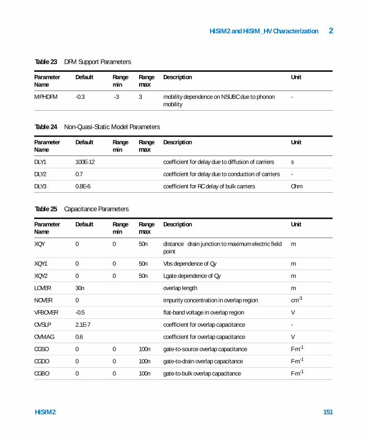
HiSIM2 and HiSIM_HV Characterization 2
Table 23 DFM Support Parameters
Parameter Name
Default Rangemin
Rangemax
Description Unit
MPHDFM -0.3 -3 3 mobility dependence on NSUBC due to phonon mobility
-
Table 24 Non-Quasi-Static Model Parameters
Parameter Name
Default Rangemin
Rangemax
Description Unit
DLY1 100E-12 coefficient for delay due to diffusion of carriers s
DLY2 0.7 coefficient for delay due to conduction of carriers -
DLY3 0.8E-6 coefficient for RC delay of bulk carriers Ohm
Table 25 Capacitance Parameters
Parameter Name
Default Rangemin
Rangemax
Description Unit
XQY 0 0 50n distance drain junction to maximum electric field point
m
XQY1 0 0 50n Vbs dependence of Qy m
XQY2 0 0 50n Lgate dependence of Qy m
LOVER 30n overlap length m
NOVER 0 impurity concentration in overlap region cm-3
VFBOVER -0.5 flat-band voltage in overlap region V
OVSLP 2.1E-7 coefficient for overlap capacitance -
OVMAG 0.6 coefficient for overlap capacitance V
CGSO 0 0 100n gate-to-source overlap capacitance F·m-1
CGDO 0 0 100n gate-to-drain overlap capacitance F·m-1
CGBO 0 0 100n gate-to-bulk overlap capacitance F·m-1
HiSIM2 151

2 HiSIM2 and HiSIM_HV Characterization
Table 26 Parasitic Resistances Parameters
Parameter Name
Default Rangemin
Rangemax
Description Unit
RS 0 0 10m source-contact resistance in LDD region Ohm·m
RD 0 0 10m drain-contact resistance in LDD region Ohm·m
RSH 0 0 1m source/drain sheet resistance Ohm/square
RSHG 0 0 100µ gate sheet resistance Ohm/square
GBMIN 1E-12 substrate resistance network -
RBPB 50 substrate resistance network Ohm
RBPD 50 substrate resistance network Ohm
RBPS 50 substrate resistance network Ohm
RBDB 50 substrate resistance network Ohm
RBSB 50 substrate resistance network Ohm
Table 27 Binning Model Parameters
Parameter Name
Default Rangemin
Rangemax
Description Unit
LBINN 1 power of Ldrawn dependence -
WBINN 1 power of Wdrawn dependence -
LMAX 1µ maximum length of Ldrawn valid µm
LMIN 1µ minimum length of Ldrawn valid µm
WMAX 1µ maximum length of Wdrawn valid µm
WMIN 1µ minimum length of Wdrawn valid µm
152 HiSIM2
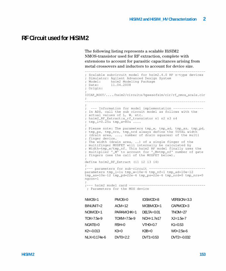
HiSIM2 and HiSIM_HV Characterization 2
RF Circuit used for HiSIM2
HiSIM2
The following listing represents a scalable HiSIM2 NMOS-transistor used for RF extraction, complete with extensions to account for parasitic capacitances arising from metal crossovers and inductors to account for device size.------------------------------------------------------------; Scalable subcircuit model for hsim2.4.0 RF n-type devices; Simulator: Agilent Advanced Design System ; Model: hsim2 Modeling Package ; Date: 11.04.2008; Origin:; ICCAP_ROOT/..../hsim2/circuits/hpeesofsim/cir/rf_nmos_scale.cir; ------------------------------------------------------------; ; --- Information for model implementation ---------------; In ADS, call the sub circuit model as follows with the; actual values of L, W, etc.; hsim2_RF_Extract:x_rf_transistor n1 n2 n3 n4 ; tmp_l=0.25u tmp_w=80u .... ; ; Please note: The parameters tmp_w, tmp_ad, tmp_as, tmp_pd,; tmp_ps, tmp_nrs, tmp_nrd always define the TOTAL width; (drain area, ..., number of drain squares) of the multi; finger device. ; The width (drain area, ..) of a single finger of the; multifinger MOSFET will internally be calculated by; Width=tmp_w/tmp_nf. This hsim2 RF model finally uses the; multiplier "_M" to account for "_M=tmp_nf" number of gate; fingers (see the call of the MOSFET below).;define hsim2_RF_Extract (i1 i2 i3 i4);;--- parameters for sub-circuit ----------------------------parameters tmp_l=1u tmp_w=10e-6 tmp_nf=1 tmp_ad=10e-12tmp_as=10e-12 tmp_pd=22e-6 tmp_ps=22e-6 tmp_nrd=0 tmp_nrs=0ngcon=1;;--- hsim2 model card -------------------------------------- ; Parameters for the MOS device
NMOS=1 PMOS=0 IDSMOD=8 VERSION=3.3
BINUNIT=2 ACM=12 MOBMOD=1 CAPMOD=3
NOIMOD=1 PARAMCHK=1 DELTA=0.01 TNOM=27
TOX=7.5e-9 TOXM=7.5e-9 NCH=1.7e17 XJ=1.5e-7
NGATE=0 RSH=0 VTH0=0.7 K1=0.53
K2=-0.013 K3=0 K3B=0 W0=2.5e-6
NLX=0.174e-6 DVT0=2.2 DVT1=0.53 DVT2=-0.032
153
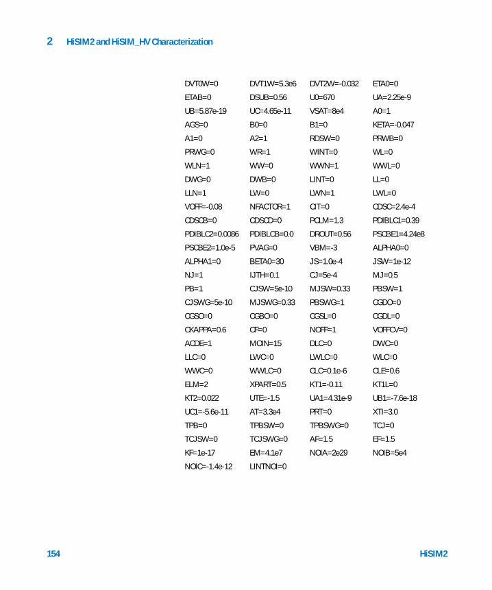
154
2 HiSIM2 and HiSIM_HV Characterization
DVT0W=0 DVT1W=5.3e6 DVT2W=-0.032 ETA0=0
ETAB=0 DSUB=0.56 U0=670 UA=2.25e-9
UB=5.87e-19 UC=4.65e-11 VSAT=8e4 A0=1
AGS=0 B0=0 B1=0 KETA=-0.047
A1=0 A2=1 RDSW=0 PRWB=0
PRWG=0 WR=1 WINT=0 WL=0
WLN=1 WW=0 WWN=1 WWL=0
DWG=0 DWB=0 LINT=0 LL=0
LLN=1 LW=0 LWN=1 LWL=0
VOFF=-0.08 NFACTOR=1 CIT=0 CDSC=2.4e-4
CDSCB=0 CDSCD=0 PCLM=1.3 PDIBLC1=0.39
PDIBLC2=0.0086 PDIBLCB=0.0 DROUT=0.56 PSCBE1=4.24e8
PSCBE2=1.0e-5 PVAG=0 VBM=-3 ALPHA0=0
ALPHA1=0 BETA0=30 JS=1.0e-4 JSW=1e-12
NJ=1 IJTH=0.1 CJ=5e-4 MJ=0.5
PB=1 CJSW=5e-10 MJSW=0.33 PBSW=1
CJSWG=5e-10 MJSWG=0.33 PBSWG=1 CGDO=0
CGSO=0 CGBO=0 CGSL=0 CGDL=0
CKAPPA=0.6 CF=0 NOFF=1 VOFFCV=0
ACDE=1 MOIN=15 DLC=0 DWC=0
LLC=0 LWC=0 LWLC=0 WLC=0
WWC=0 WWLC=0 CLC=0.1e-6 CLE=0.6
ELM=2 XPART=0.5 KT1=-0.11 KT1L=0
KT2=0.022 UTE=-1.5 UA1=4.31e-9 UB1=-7.6e-18
UC1=-5.6e-11 AT=3.3e4 PRT=0 XTI=3.0
TPB=0 TPBSW=0 TPBSWG=0 TCJ=0
TCJSW=0 TCJSWG=0 AF=1.5 EF=1.5
KF=1e-17 EM=4.1e7 NOIA=2e29 NOIB=5e4
NOIC=-1.4e-12 LINTNOI=0
HiSIM2

HiSIM2 and HiSIM_HV Characterization 2
HiSIM2
;--- Additional model parameters necessary for scalability--; - scalable external capacitors taking into account cross; coupling between metal lines and inductors to account for; delay effects due to the size of the devices; - scalable channel length reduction in multi finger devices; - a scalable substrate network and scalable Delta L reduction
CGDEXT0=1e-9 ;external capacitance gate-drain per gate width and gate finger [F/m]CGSEXT0=1e-9 ;external capacitance gate-source per gate width and gate finger ; [F/m]CDSEXT0=1e-9 ;external capacitance drain-source per gate width and gate finger; [F/m]RSHG=25 ; gate sheet resistance [Ohm sq]LDRAIN0=1e-6 ; drain inductance per gate width and gate finger [H/m]LGATE0=1e-6 ; gate inductance per gate width and gate finger [H/m]LSOURCE0=1e-6 ; source inductance per gate width and gate finger [H/m]LBULK0=1e-6 ; bulk inductance per gate width and gate finger [H/m]RSHB=25 ; bulk sheet resistance [Ohm sq]DSBC=2e-6 ; distance source implant to bulk contact [m]DDBC=2e-6 ; distance drain implant to bulk contact [m]DGG=2e-6 ; distance gate to gate [m]DL0=0 ; basic channel length reduction correction [m] DL1=0 ; channel length reduction correction 1. and 2. fingers [m]DL2=0 ; channel length reduction correction outer fingers [m];; --- internal temporary variablesfactor_even_odd = 0.5*(1+(tmp_nf-2*int(0.5*tmp_nf)))tmp_dl1 = (tmp_nf-4.5)/(2*abs(tmp_nf-4.5)) * 8/ tmp_nftmp_dl2 = (tmp_nf-2.5)/(2*abs(tmp_nf-2.5)) * 4/ tmp_nfLeff = tmp_l - 2*(DL0+tmp_dl1*DL1+tmp_dl2*DL2) ; ; --------- Gate network ------------------------------C:CGDEXT n20 n10 C=CGDEXT0*tmp_wC:CGSEXT n20 n30 C=CGSEXT0*tmp_wR:RGATE n20 n21 + R=(0.333*RSHG*tmp_w/(tmp_l*tmp_nf*tmp_nf*ngcon^2)) Noise=1L:LGATE i2 n20 L=LGATE0*tmp_w; --------- Drain network -----------------------------C:CDSEXT n10 n30 C=CDSEXT0*tmp_wL:LDRAIN i1 n10 L=LDRAIN0*tmp_w; --------- Source network -----------------------------L:LSOURCE i3 n30 L=LSOURCE0*tmp_w; --------- Substrate network ------------------------- ; Diodes are for n-type MOS transistors
155
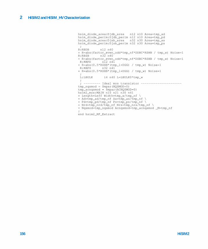
156
2 HiSIM2 and HiSIM_HV Characterization
hsim_diode_area:Djdb_area n12 n10 Area=tmp_adhsim_diode_perim:Djdb_perim n12 n10 Area=tmp_pdhsim_diode_area:Djsb_area n32 n30 Area=tmp_ashsim_diode_perim:Djsb_perim n32 n30 Area=tmp_ps ;R:RBDB n12 n40 + R=abs(factor_even_odd*tmp_nf*DDBC*RSHB / tmp_w) Noise=1R:RBSB n32 n40 + R=abs(factor_even_odd*tmp_nf*DSBC*RSHB / tmp_w) Noise=1 R:RBPD n12 n41 + R=abs(0.5*RSHB*(tmp_l+DGG) / tmp_w) Noise=1 R:RBPS n32 n41 + R=abs(0.5*RSHB*(tmp_l+DGG) / tmp_w) Noise=1 ; L:LBULK i4 n40 L=LBULK0*tmp_w ; ; --------- Ideal mos transistor ----------------------tmp_nqsmod = $mpar(NQSMOD=0)tmp_acnqsmod = $mpar(ACNQSMOD=0)hsim2_mos:MAIN n10 n21 n30 n41 + Length=Leff Width=tmp_w/tmp_nf \+ Ad=tmp_ad/tmp_nf As=tmp_as/tmp_nf \+ Pd=tmp_pd/tmp_nf Ps=tmp_ps/tmp_nf \+ Nrd=tmp_nrd/tmp_nf Nrs=tmp_nrs/tmp_nf \+ Nqsmod=tmp_nqsmod Acnqsmod=tmp_acnqsmod _M=tmp_nf;end hsim2_RF_Extract
HiSIM2
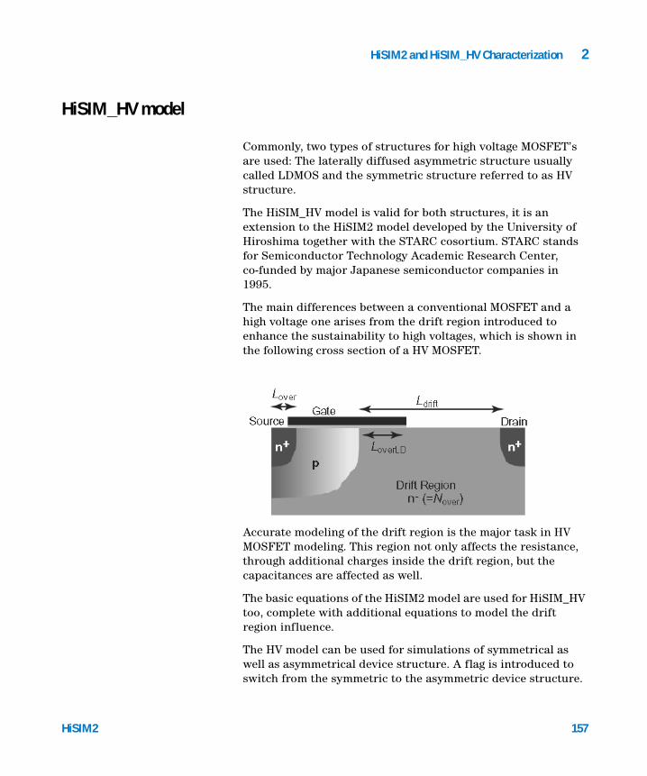
HiSIM2 and HiSIM_HV Characterization 2
HiSIM_HV model
HiSIM2
Commonly, two types of structures for high voltage MOSFET’s are used: The laterally diffused asymmetric structure usually called LDMOS and the symmetric structure referred to as HV structure.
The HiSIM_HV model is valid for both structures, it is an extension to the HiSIM2 model developed by the University of Hiroshima together with the STARC cosortium. STARC stands for Semiconductor Technology Academic Research Center, co-funded by major Japanese semiconductor companies in 1995.
The main differences between a conventional MOSFET and a high voltage one arises from the drift region introduced to enhance the sustainability to high voltages, which is shown in the following cross section of a HV MOSFET.
Accurate modeling of the drift region is the major task in HV MOSFET modeling. This region not only affects the resistance, through additional charges inside the drift region, but the capacitances are affected as well.
The basic equations of the HiSIM2 model are used for HiSIM_HV too, complete with additional equations to model the drift region influence.
The HV model can be used for simulations of symmetrical as well as asymmetrical device structure. A flag is introduced to switch from the symmetric to the asymmetric device structure.
157

158
2 HiSIM2 and HiSIM_HV Characterization
COSYM=0 refers to the asymmetric LDMOS structure, COSYM=1 to the symmetric HVMOS structure. The following figure shows the parameter extraction approach using the COSYM parameter.
HiSIM_HV solves the Poisson equation iteratively, including the highly resistive drift region effects, depending on the structure of the MOS transistor to be modeled.
The cross section (Figure 47) through a LDMOS and a HVMOS structure shows the drift region resistance parameters and their usage.
HiSIM2
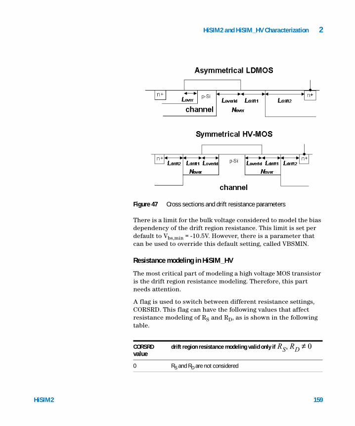
HiSIM2 and HiSIM_HV Characterization 2
HiSIM2
Figure 47 Cross sections and drift resistance parameters
There is a limit for the bulk voltage considered to model the bias dependency of the drift region resistance. This limit is set per default to Vbs,min = -10.5V. However, there is a parameter that can be used to override this default setting, called VBSMIN.
Resistance modeling in HiSIM_HV
The most critical part of modeling a high voltage MOS transistor is the drift region resistance modeling. Therefore, this part needs attention.
A flag is used to switch between different resistance settings, CORSRD. This flag can have the following values that affect resistance modeling of RS and RD, as is shown in the following table.
CORSRD value
drift region resistance modeling valid only if
0 RS and RD are not considered
RS RD, 0≠
159
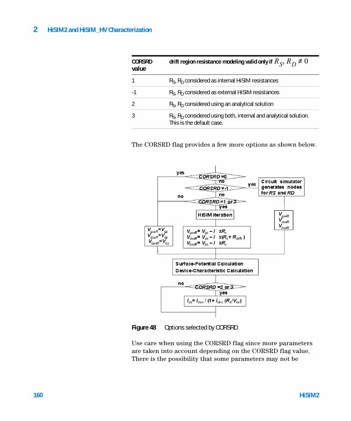
160
2 HiSIM2 and HiSIM_HV Characterization
The CORSRD flag provides a few more options as shown below.
Figure 48 Options selected by CORSRD
Use care when using the CORSRD flag since more parameters are taken into account depending on the CORSRD flag value. There is the possibility that some parameters may not be
1 RS, RD considered as internal HiSIM resistances
-1 RS, RD considered as external HiSIM resistances
2 RS, RD considered using an analytical solution
3 RS, RD considered using both, internal and analytical solution. This is the default case.
CORSRD value
drift region resistance modeling valid only if RS RD, 0≠
HiSIM2
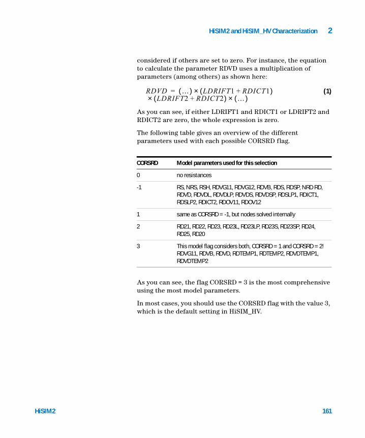
HiSIM2 and HiSIM_HV Characterization 2
HiSIM2
considered if others are set to zero. For instance, the equation to calculate the parameter RDVD uses a multiplication of parameters (among others) as shown here:
(1)
As you can see, if either LDRIFT1 and RDICT1 or LDRIFT2 and RDICT2 are zero, the whole expression is zero.
The following table gives an overview of the different parameters used with each possible CORSRD flag.
As you can see, the flag CORSRD = 3 is the most comprehensive using the most model parameters.
In most cases, you should use the CORSRD flag with the value 3, which is the default setting in HiSIM_HV.
CORSRD Model parameters used for this selection
0 no resistances
-1 RS, NRS, RSH, RDVG11, RDVG12, RDVB, RDS, RDSP, NRD RD, RDVD, RDVDL, RDVDLP, RDVDS, RDVDSP, RDSLP1, RDICT1, RDSLP2, RDICT2, RDOV11, RDOV12
1 same as CORSRD = -1, but nodes solved internally
2 RD21, RD22, RD23, RD23L, RD23LP, RD23S, RD23SP, RD24, RD25, RD20
3 This model flag considers both, CORSRD = 1 and CORSRD = 2!RDVG11, RDVB, RDVD, RDTEMP1, RDTEMP2, RDVDTEMP1, RDVDTEMP2
RDVD …( ) LDRIFT1 RDICT1+( )×LDRIFT2 RDICT2+( )× …( )×
=
161
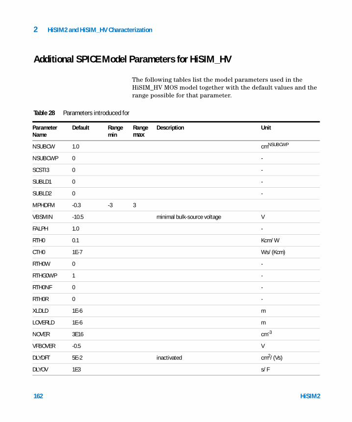
2 HiSIM2 and HiSIM_HV Characterization
Additional SPICE Model Parameters for HiSIM_HV
162
The following tables list the model parameters used in the HiSIM_HV MOS model together with the default values and the range possible for that parameter.
Table 28 Parameters introduced for
Parameter Name
Default Rangemin
Rangemax
Description Unit
NSUBCW 1.0 cmNSUBCWP
NSUBCWP 0 -
SCSTI3 0 -
SUBLD1 0 -
SUBLD2 0 -
MPHDFM -0.3 -3 3
VBSMIN -10.5 minimal bulk-source voltage V
FALPH 1.0 -
RTH0 0.1 Kcm/W
CTH0 1E-7 Ws/(Kcm)
RTH0W 0 -
RTHG0WP 1 -
RTH0NF 0 -
RTH0R 0 -
XLDLD 1E-6 m
LOVERLD 1E-6 m
NOVER 3E16 cm-3
VFBOVER -0.5 V
DLYDFT 5E-2 inactivated cm2/(Vs)
DLYOV 1E3 s/F
HiSIM2

HiSIM2 and HiSIM_HV Characterization 2
QOVSM 0.2 for smoothing of Qover -
LDRIFT 1E-6 length of the drift region m
RDVG11 100m -
RDVG12 100 -
RDVD 1E-2
RDVB 0 -
RDS 0 -
RDSP 1 -
RDVDL 0 -
RDVDP 1 -
RDVDS 0 -
RDVDSP 1 -
RD20 0 -
RD21 1 -
RD22 0
RD23 0.5
RD23L 0 -
RD23LP 1 -
RD23S 0 -
RD23SP 1 -
RD24 0
RD25 0 V
Table 28 (continued)Parameters introduced for
Parameter Name
Default Rangemin
Rangemax
Description Unit
Ω V⁄
Ωm V⁄
Ωm VRD21⁄
Ωm VRD21 1+⁄
HiSIM2 163
2 HiSIM2 and HiSIM_HV Characterization
References
164
1 HiSIM Web Site: http://home.hiroshima-u.ac.jp/usdl/HiSIM.html
2 H.J.Mattausch et al., “Accuracy and Speed Performance of HiSIM Versions 231 and 240”, Compact Modeling for CMOS/Nano Technologies, MOS-AK / ESSDERC / ESSCIRC Workshop, Munich, Germany, September 14th, 2007
3 M.Miura-Mattausch et al.: “HiSIM: Self-Consistent Surface- Potential MOS-Model Valid Down to Sub-100nm Technologies”, Technical Proceedings of the 2002 International Conference on Modeling and Simulation of Microsystems, Vol.1 (Nanotech 2002), P. 678 - 681, NSTI Nano Science and Technology Institute 2002, Cambridge, Massachusetts, USA; also to be found at: http://www.nsti.org/procs/MSM2002/13/T41.03
HiSIM2

Agilent 85190A IC-CAP 2008Nonlinear Device Models Volume 1
3PSP Characterization
Overview of the PSP model 166
PSP Modeling Package 168
Extraction of Parameters for the PSP Model 169
Simultaneous Adjustment of Local and Global Parameters 176
Binning of PSP Models 188
Parameters for the PSP model 197
This chapter provides a theoretical background for the PSP model. It is based on model revision PSP102.0, released in June 2006.
Using the Modeling Packages is described in Chapter 1, “Using the MOS Modeling Packages.”
The PSP model is a compact MOSFET model intended for digital, analog, and RF design. PSP is a surface-potential based model and includes all relevant physical effects (mobility reduction, velocity saturation, DIBL, gate current, lateral doping gradient effects, STI stress, etc.) needed to model deep submicron bulk CMOS technologies. A source/drain junction model, the JUNCAP2 model, is an integrated part of PSP.
In December 2005, the Compact Model Council (CMC) selected PSP as the new industrial standard model for compact MOSFET modeling.
The PSP source code, user manual, and testing examples can be downloaded at: http://pspmodel.asu.edu
or at
http://www.nxp.com/Philips_Models/mos_models/psp
165Agilent Technologies

3 PSP Characterization
Overview of the PSP model
166
The PSP model uses a hierarchical structure and therefore a global and local parameter set. A separation exists between the scaling rules used for the global model and the parameters of the local model. The model can be used at each of the levels.
Global Level
A global parameter set is used to model a range of geometries used in a given process. Combined with instance parameters L and W, from the global parameter set a local model will be derived and processed subsequently at the local level for each geometry.
Local Level
A local parameter set is used to simulate one discrete geometry. At this level, the temperature scaling is included.
Each of the parameters of the local parameter set can be derived from electrical measurements. Consequently, a local parameter set gives a complete description of one device for a specific geometry.
Most of these local parameters scale with geometry. A whole range of geometries used in a MOS process can therefore be described by a larger set of parameters, the global parameter set.
IC-CAP Nonlinear Device Models Volume 1
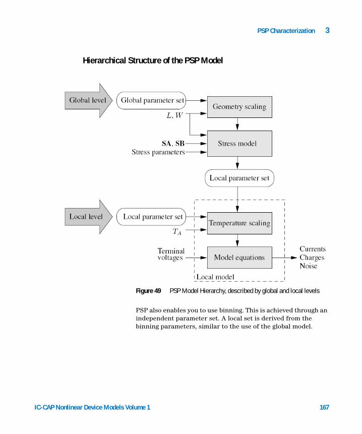
PSP Characterization 3
Hierarchical Structure of the PSP Model
IC-CAP Nonlinear Device Models Vo
PSP also enables you to use binning. This is achieved through an independent parameter set. A local set is derived from the binning parameters, similar to the use of the global model.
Figure 49 PSP Model Hierarchy, described by global and local levels
lume 1 167
3 PSP Characterization
PSP Modeling Package
168
The PSP Modeling Package uses the same graphic user interface as is used in extracting BSIM3 and BSIM4 model parameters. Therefore, the handling is the same and is described in Chapter 1, “Using the MOS Modeling Packages.
• The graphical user interface enables the quick setup of tests and measurements followed by automatic parameter extraction routines.
• The data management concept allows a powerful and flexible handling of measurement data using an open and easy data base concept.
• The extraction procedures can be adapted to different needs. Although the extraction procedure is recommended by the model developers and has been followed by the standard extraction flow inside the PSP Modeling Package, experienced users can change the flow.
NOTE Since extracting the parameters for the global model depends on the extraction sequence, only the experienced user should manipulate the default extraction flow, which is based on the recommendations of the PSP User’s Manual.
The next section provides a detailed description of the extraction sequence.
IC-CAP Nonlinear Device Models Volume 1

PSP Characterization 3
Extraction of Parameters for the PSP Model
IC-CAP Nonlinear Device Models Vo
Because of correlations, you should not derive all local parameters for a specific device simultaneously. The model developers outline a practical extraction sequence. This recommendation is the base for the default extraction flow programmed into the PSP Modeling Toolkit. The following describes the sequence of parameter extraction used in the toolkit.
For every device, the extraction of local parameters must be performed. However, not every local parameter for all devices must be extracted. Some parameters are extracted for only one device. Other parameters are extracted for a few devices and are fixed for other devices. A number of parameters can be kept fixed at default values and only optimized in fine tuning steps during extraction. Note, that for all extractions, the reference temperature TR must be set to the actual room temperature the devices are measured under.
Before extraction, switch parameters SWIGATE, SWIMPACT, SWGIDL, SWJUNCAP, and TYPE are set to appropriate values and QMC is set to 1 to include quantum mechanical corrections.
Some parameters influencing the DC behavior of a MOSFET are extracted accurately only from CV measurements (NP, for example).
In order to get good DC parameter values, you should start from the default parameter set and use a value of TOX as is known from technology. With this settings, extractions of VFB, NEFF, DPHIB, NP, and COX can be done using the measurement of CGG vs. VGS of the long, wide device.
The extraction process starts with local parameters for the Long/Wide device, followed by extraction of local parameters for the rest of the devices with max. length. Then there is a global parameter extraction/optimization step involving all devices of max. length. The next step uses the Short/Wide device (same width, but shortest length) to extract local parameters and so on. The following figure is a graphical representation of the extraction sequence. The numbers show
lume 1 169
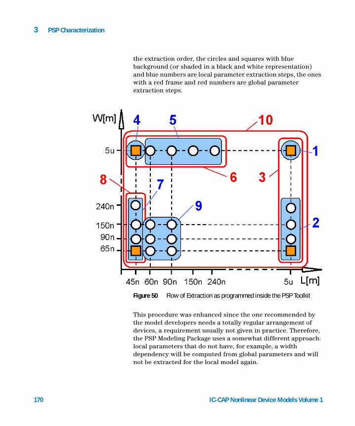
170
3 PSP Characterization
the extraction order, the circles and squares with blue background (or shaded in a black and white representation) and blue numbers are local parameter extraction steps, the ones with a red frame and red numbers are global parameter extraction steps.
This procedure was enhanced since the one recommended by the model developers needs a totally regular arrangement of devices, a requirement usually not given in practice. Therefore, the PSP Modeling Package uses a somewhat different approach: local parameters that do not have, for example, a width dependency will be computed from global parameters and will not be extracted for the local model again.
Figure 50 Flow of Extraction as programmed inside the PSP Toolkit
IC-CAP Nonlinear Device Models Volume 1
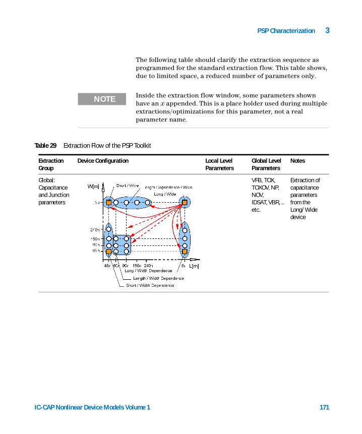
PSP Characterization 3
IC-CAP Nonlinear Device Models Vo
The following table should clarify the extraction sequence as programmed for the standard extraction flow. This table shows, due to limited space, a reduced number of parameters only.
NOTE Inside the extraction flow window, some parameters shown have an x appended. This is a place holder used during multiple extractions/optimizations for this parameter, not a real parameter name.
Toolkit
Table 29 Extraction Flow of the PSP
Extraction Group
Device Configuration Local Level Parameters
Global Level Parameters
Notes
Global:Capacitance and Junction parameters
VFB, TOX, TOXOV, NP, NOV,IDSAT, VBR, .. etc.
Extraction of capacitance parameters from the Long/Wide device
lume 1 171
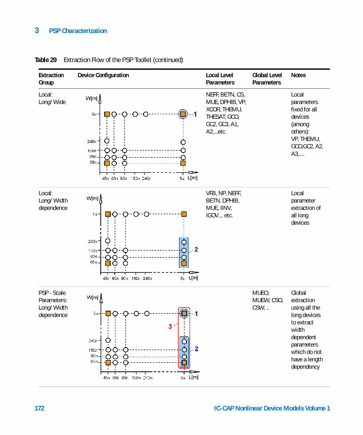
3 PSP Characterization
Local:Long/Wide
NEFF, BETN, CS, MUE, DPHIB, VP, XCOR, THEMU, THESAT, GCO, GC2, GC3, A1, A2,...etc.
Local parameters fixed for all devices (among others):VP, THEMU, GCO,GC2, A2, A3,....
Local:Long/Width dependence
VFB, NP, NEFF, BETN, DPHIB, MUE, IINV, IGOV.... etc.
Local parameter extraction of all long devices
PSP - Scale Parameters:Long/Width dependence
MUEO, MUEW, CSO, CSW, ..
Global extraction using all the long devices to extract width dependent parameters which do not have a length dependency
Table 29 Extraction Flow of the PSP Toolkit (continued)
Extraction Group
Device Configuration Local Level Parameters
Global Level Parameters
Notes
172 IC-CAP Nonlinear Device Models Volume 1
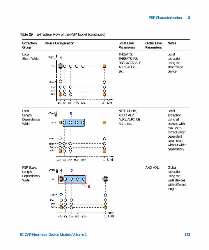
PSP Characterization 3
Local:Short/Wide
THESATG, THESATB, RS, RSB, XCOR, ALP, ALP1, ALP2, .... etc.
Local extraction using the short/wide device
Local:Length Dependence/ Wide
NEFF, DPHIB, XCOR, ALP, ALP1, ALP2, CF, AX .... etc.
Local extraction using all devices with max. W to extract length dependent parameters without width dependency
PSP Scale:Length Dependence/ Wide
AXO, AXL Global extraction using the wide devices with different length
Table 29 Extraction Flow of the PSP Toolkit (continued)
Extraction Group
Device Configuration Local Level Parameters
Global Level Parameters
Notes
IC-CAP Nonlinear Device Models Volume 1 173
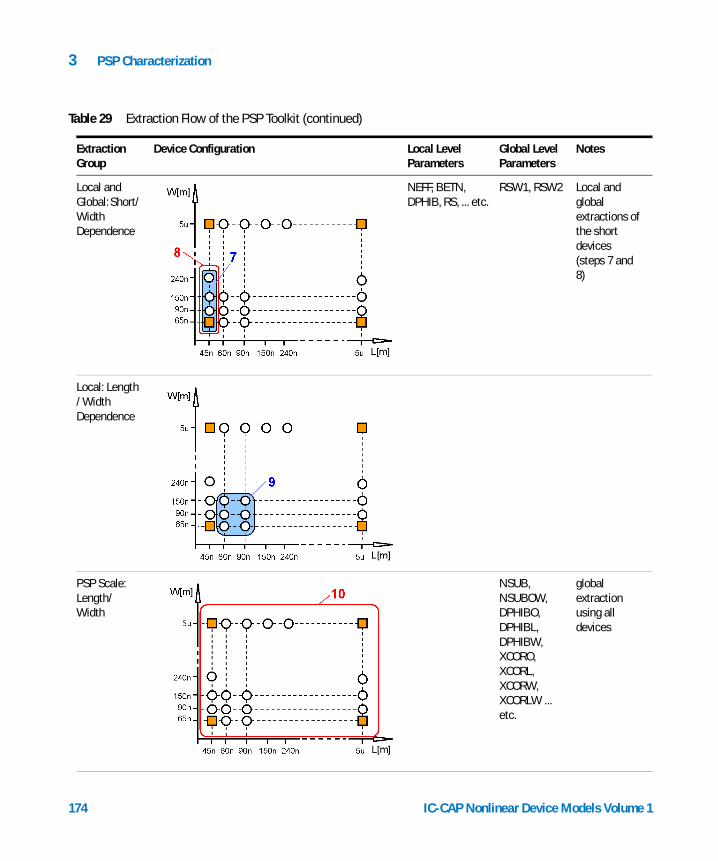
3 PSP Characterization
Local and Global: Short/ Width Dependence
NEFF, BETN, DPHIB, RS, ... etc.
RSW1, RSW2 Local and global extractions of the short devices (steps 7 and 8)
Local: Length /Width Dependence
PSP Scale: Length/ Width
NSUB, NSUBOW, DPHIBO, DPHIBL, DPHIBW, XCORO, XCORL, XCORW, XCORLW ... etc.
global extraction using all devices
Table 29 Extraction Flow of the PSP Toolkit (continued)
Extraction Group
Device Configuration Local Level Parameters
Global Level Parameters
Notes
174 IC-CAP Nonlinear Device Models Volume 1
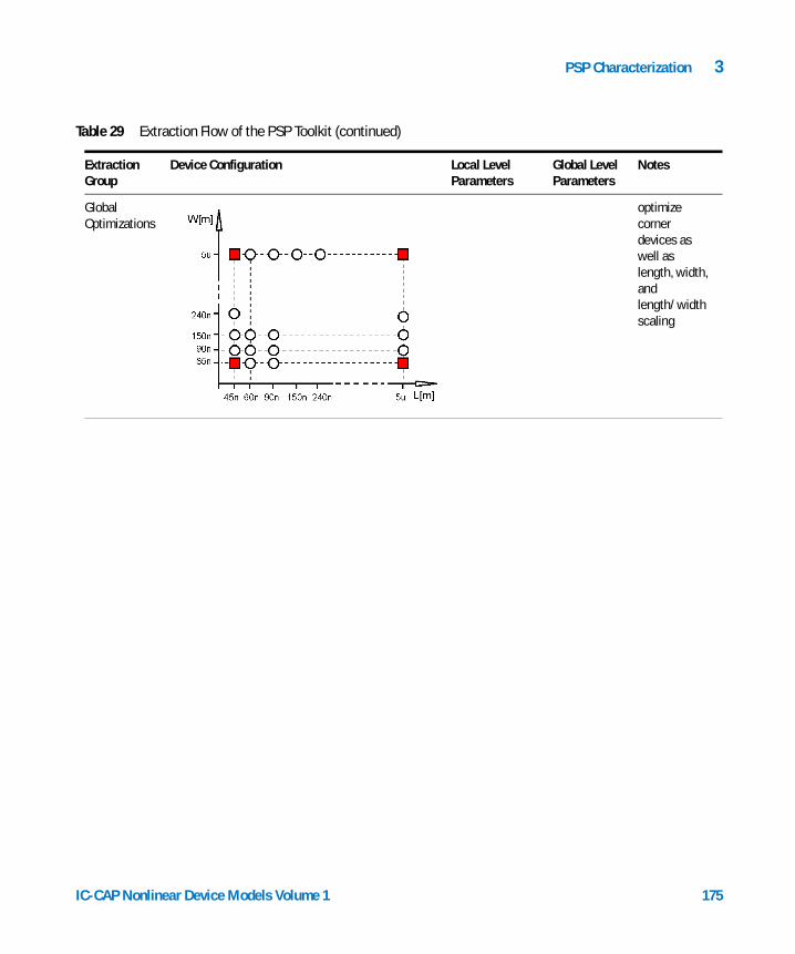
PSP Characterization 3
Global Optimizations
optimize corner devices as well as length, width, and length/width scaling
Table 29 Extraction Flow of the PSP Toolkit (continued)
Extraction Group
Device Configuration Local Level Parameters
Global Level Parameters
Notes
IC-CAP Nonlinear Device Models Volume 1 175
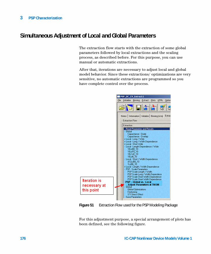
3 PSP Characterization
Simultaneous Adjustment of Local and Global Parameters
176
The extraction flow starts with the extraction of some global parameters followed by local extractions and the scaling process, as described before. For this purpose, you can use manual or automatic extractions.
After that, iterations are necessary to adjust local and global model behavior. Since these extractions/ optimizations are very sensitive, no automatic extractions are programmed so you have complete control over the process.
For this adjustment purpose, a special arrangement of plots has been defined, see the following figure.
Figure 51 Extraction Flow used for the PSP Modeling Package
IC-CAP Nonlinear Device Models Volume 1
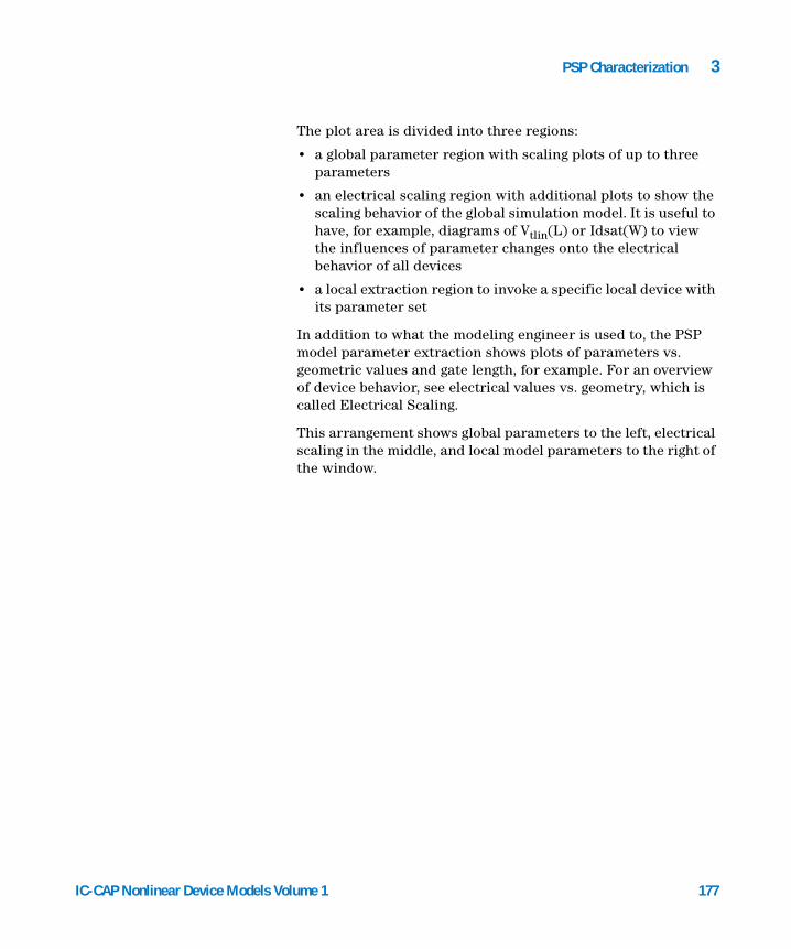
PSP Characterization 3
IC-CAP Nonlinear Device Models Vo
The plot area is divided into three regions:
• a global parameter region with scaling plots of up to three parameters
• an electrical scaling region with additional plots to show the scaling behavior of the global simulation model. It is useful to have, for example, diagrams of Vtlin(L) or Idsat(W) to view the influences of parameter changes onto the electrical behavior of all devices
• a local extraction region to invoke a specific local device with its parameter set
In addition to what the modeling engineer is used to, the PSP model parameter extraction shows plots of parameters vs. geometric values and gate length, for example. For an overview of device behavior, see electrical values vs. geometry, which is called Electrical Scaling.
This arrangement shows global parameters to the left, electrical scaling in the middle, and local model parameters to the right of the window.
lume 1 177
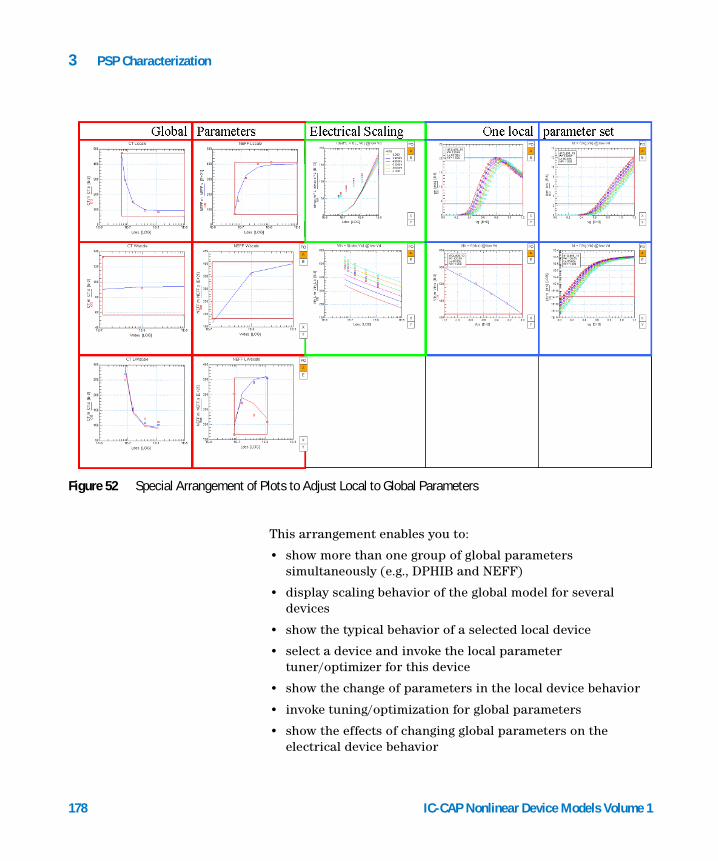
3 PSP Characterization
Figure 52 Special Arrangement of Plots to Adjust Local to Global Parameters
178
This arrangement enables you to:
• show more than one group of global parameters simultaneously (e.g., DPHIB and NEFF)
• display scaling behavior of the global model for several devices
• show the typical behavior of a selected local device
• select a device and invoke the local parameter tuner/optimizer for this device
• show the change of parameters in the local device behavior
• invoke tuning/optimization for global parameters
• show the effects of changing global parameters on the electrical device behavior
IC-CAP Nonlinear Device Models Volume 1
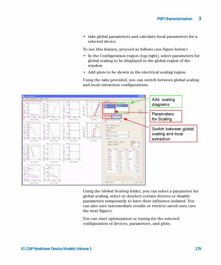
PSP Characterization 3
IC-CAP Nonlinear Device Models Vo
• take global parameters and calculate local parameters for a selected device
To use this feature, proceed as follows (see figure below):
• In the Configuration region (top right), select parameters for global scaling to be displayed in the global region of the window
• Add plots to be shown in the electrical scaling region
Using the tabs provided, you can switch between global scaling and local extraction configurations.
Using the Global Scaling folder, you can select a parameter for global scaling, select or deselect certain devices or disable parameters temporarily to have their influence isolated. You can also save intermediate results or retrieve saved ones (see the next figure).
You can start optimization or tuning for the selected configuration of devices, parameters, and plots.
lume 1 179
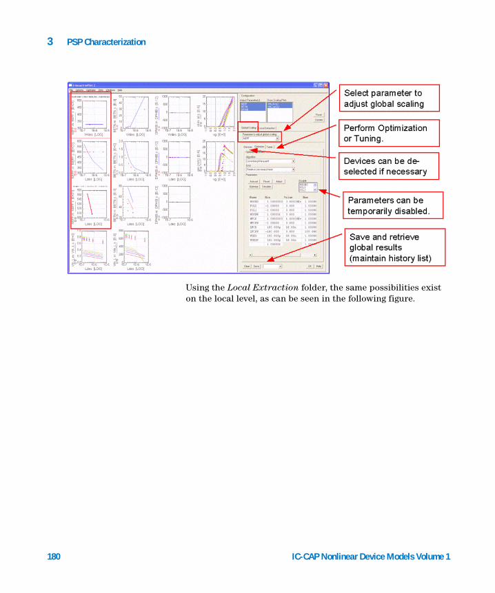
3 PSP Characterization
180
Using the Local Extraction folder, the same possibilities exist on the local level, as can be seen in the following figure.
IC-CAP Nonlinear Device Models Volume 1
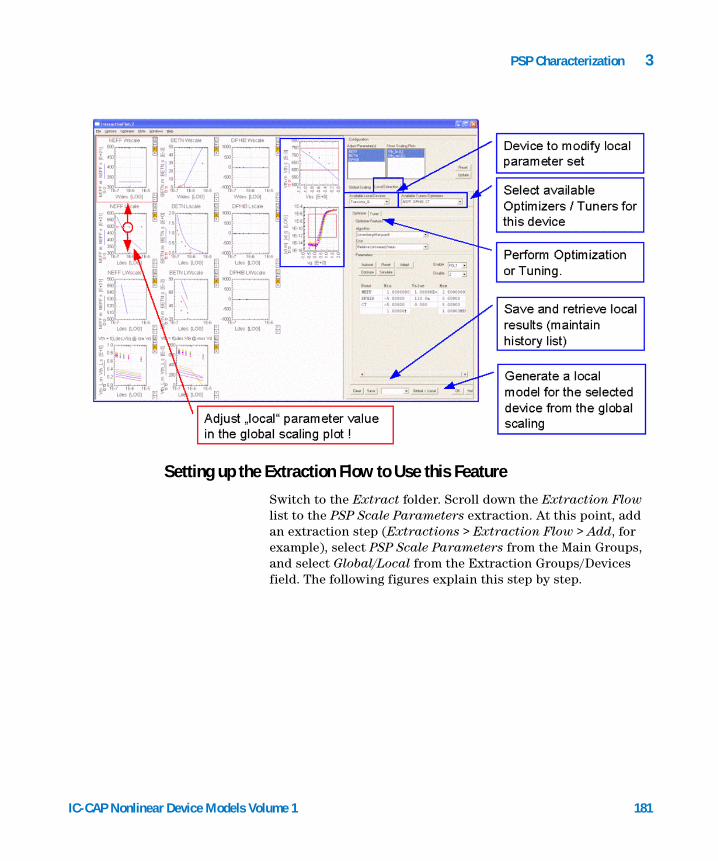
PSP Characterization 3
IC-CAP Nonlinear Device Models Vo
Setting up the Extraction Flow to Use this Feature
Switch to the Extract folder. Scroll down the Extraction Flow list to the PSP Scale Parameters extraction. At this point, add an extraction step (Extractions > Extraction Flow > Add, for example), select PSP Scale Parameters from the Main Groups, and select Global/Local from the Extraction Groups/Devices field. The following figures explain this step by step.
lume 1 181
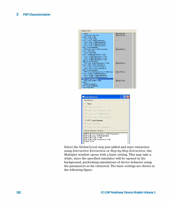
182
3 PSP Characterization
Select the Global/Local step just added and start extraction using Interactive Extraction or Step-by-Step Extraction—the Multiplot window opens with a basic setting. This may take a while, since the specified simulator will be opened in the background, performing simulations of device behavior using the parameters so far extracted. The basic settings are shown in the following figure.
IC-CAP Nonlinear Device Models Volume 1
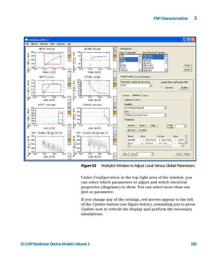
PSP Characterization 3
IC-CAP Nonlinear Device Models Vo
Under Configuration in the top right area of the window, you can select which parameters to adjust and which electrical properties (diagrams) to show. You can select more than one plot or parameter.
If you change any of the settings, red arrows appear to the left of the Update button (see figure below), reminding you to press Update now to refresh the display and perform the necessary simulations.
Figure 53 Multiplot Window to Adjust Local Versus Global Parameters
lume 1 183
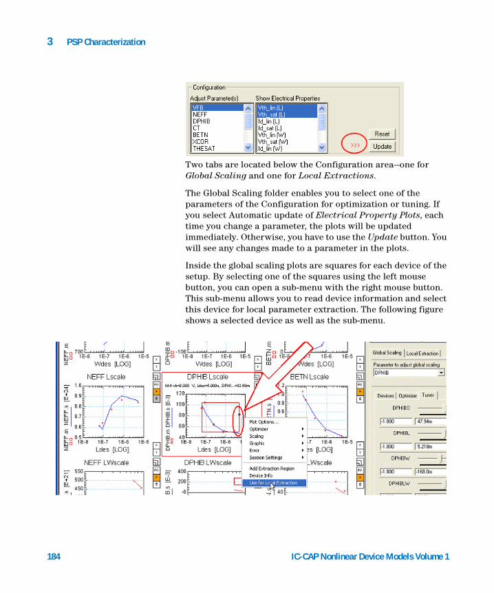
184
3 PSP Characterization
Two tabs are located below the Configuration area—one for Global Scaling and one for Local Extractions.
The Global Scaling folder enables you to select one of the parameters of the Configuration for optimization or tuning. If you select Automatic update of Electrical Property Plots, each time you change a parameter, the plots will be updated immediately. Otherwise, you have to use the Update button. You will see any changes made to a parameter in the plots.
Inside the global scaling plots are squares for each device of the setup. By selecting one of the squares using the left mouse button, you can open a sub-menu with the right mouse button. This sub-menu allows you to read device information and select this device for local parameter extraction. The following figure shows a selected device as well as the sub-menu.
IC-CAP Nonlinear Device Models Volume 1
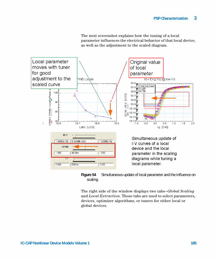
PSP Characterization 3
IC-CAP Nonlinear Device Models Vo
The next screenshot explains how the tuning of a local parameter influences the electrical behavior of that local device, as well as the adjustment to the scaled diagram.
The right side of the window displays two tabs—Global Scaling and Local Extraction. Those tabs are used to select parameters, devices, optimizer algorithms, or tuners for either local or global devices.
Figure 54 Simultaneous update of local parameter and the influence on scaling
lume 1 185
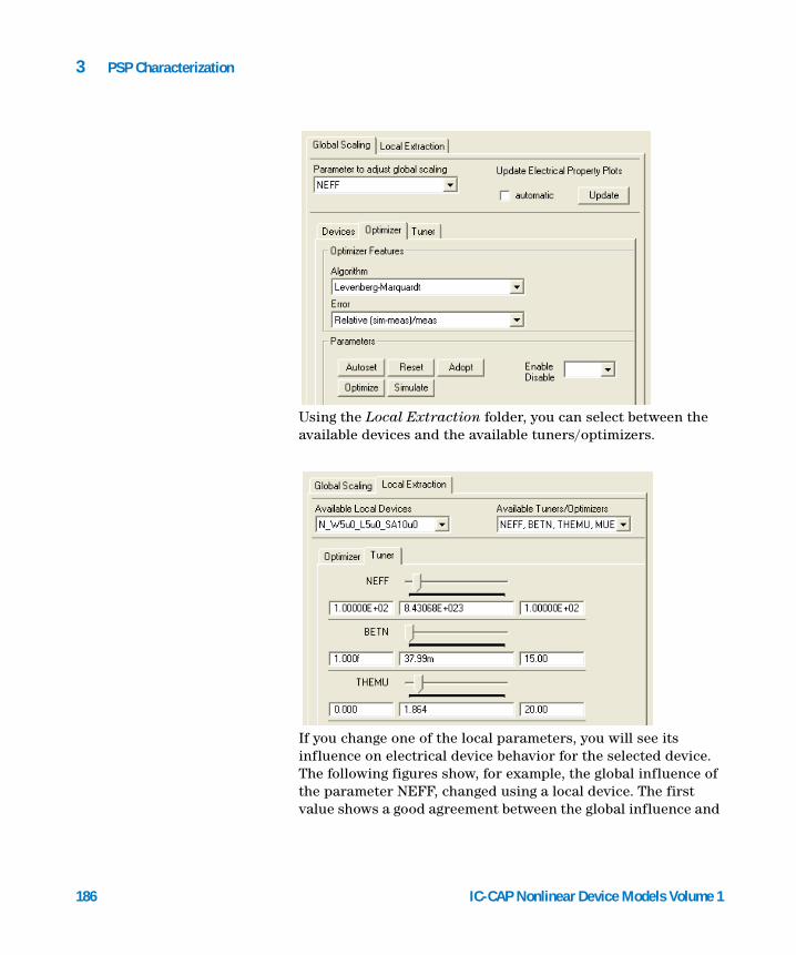
186
3 PSP Characterization
Using the Local Extraction folder, you can select between the available devices and the available tuners/optimizers.
If you change one of the local parameters, you will see its influence on electrical device behavior for the selected device. The following figures show, for example, the global influence of the parameter NEFF, changed using a local device. The first value shows a good agreement between the global influence and
IC-CAP Nonlinear Device Models Volume 1
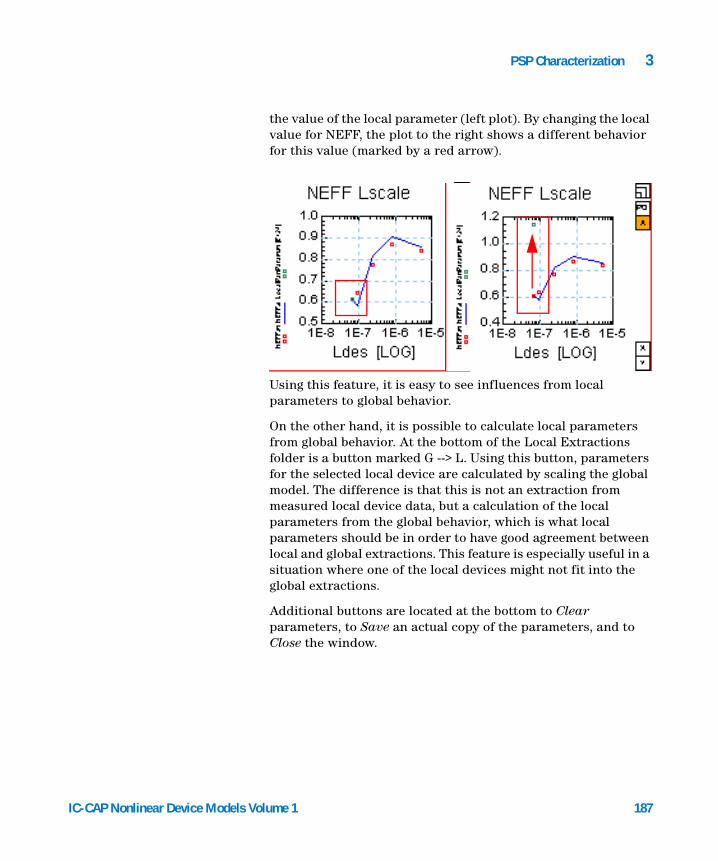
PSP Characterization 3
IC-CAP Nonlinear Device Models Vo
the value of the local parameter (left plot). By changing the local value for NEFF, the plot to the right shows a different behavior for this value (marked by a red arrow).
Using this feature, it is easy to see influences from local parameters to global behavior.
On the other hand, it is possible to calculate local parameters from global behavior. At the bottom of the Local Extractions folder is a button marked G --> L. Using this button, parameters for the selected local device are calculated by scaling the global model. The difference is that this is not an extraction from measured local device data, but a calculation of the local parameters from the global behavior, which is what local parameters should be in order to have good agreement between local and global extractions. This feature is especially useful in a situation where one of the local devices might not fit into the global extractions.
Additional buttons are located at the bottom to Clear parameters, to Save an actual copy of the parameters, and to Close the window.
lume 1 187
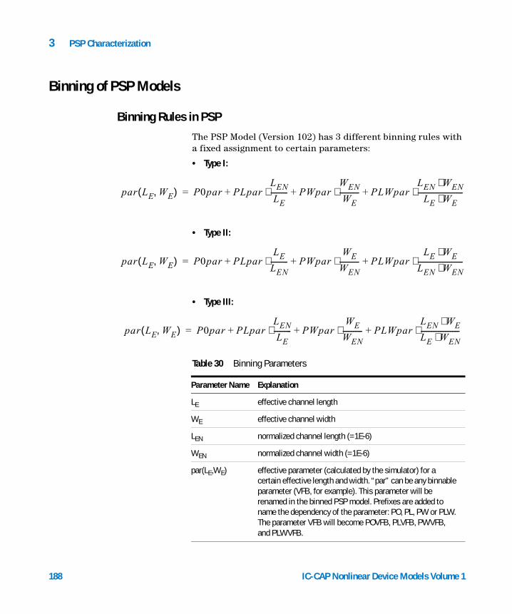
3 PSP Characterization
Binning of PSP Models
Binning Rules in PSP
188
par LE WE,( ) =
par LE WE,( ) =
par LE WE,( )
The PSP Model (Version 102) has 3 different binning rules with a fixed assignment to certain parameters:
• Type I:
• Type II:
• Type III:
Table 30 Binning Parameters
Parameter Name Explanation
LE effective channel length
WE effective channel width
LEN normalized channel length (=1E-6)
WEN normalized channel width (=1E-6)
par(LE,WE) effective parameter (calculated by the simulator) for a certain effective length and width. “par” can be any binnable parameter (VFB, for example). This parameter will be renamed in the binned PSP model. Prefixes are added to name the dependency of the parameter: PO, PL, PW or PLW. The parameter VFB will become POVFB, PLVFB, PWVFB, and PLWVFB.
P0par PLparLEN
LE----------⋅ PWpar
WEN
WE-----------⋅ PLWpar
LEN WEN⋅LE WE⋅
--------------------------⋅+ + +
P0par PLparLE
LEN----------⋅ PWpar
WE
WEN-----------⋅ PLWpar
LE WE⋅LEN WEN⋅--------------------------⋅+ + +
P0par PLparLEN
LE----------⋅ PWpar
WE
WEN-----------⋅ PLWpar
LEN WE⋅LE WEN⋅----------------------⋅+ + +=
IC-CAP Nonlinear Device Models Volume 1
PSP Characterization 3
IC-CAP Nonlinear Device Models Vo
Channel length reduction LE, WE are calculated as:
(2)
(3)
The parameter LAP in Equation 2 is defined as the effective channel length reduction, the parameter WOT in Equation 3 as the effective channel width reduction due to lateral diffusion of channel stop implant ions.
In contrast to BSIM4, the model parameters of the binned PSP model originate from 2 different sources: The local and the global model. The table below describes the source of the final binning parameters and whether an extension (PO, PL, PW, PLW) is to be added.
LE L ∆LPS 2LAP–+=
∆LPS LVARO 1 LVARLLEN
L----------⋅+
1 LVARWWEN
W-----------⋅+
⋅ ⋅=
WE W ∆WOD 2WOT–+=
∆WOD WVARO 1 WVARLLEN
L----------⋅+
1 WVARWWEN
W-----------⋅+
⋅ ⋅=
Name Parameter name in local or global model
Parameter name in final binned circuit
Comment
Simulator specific parameter Level = 1020 Level = 1021
Parameter from a local circuit which is binned
VFB POVFB, PLVFB, PWVFB, PLWVFB
Parameter from a local circuit which could be binned but is actually identical in all local devices.
VFB POVFB only the constant part will be calculated
Parameter from a local circuit which is not binned but changes his name
NSUB PONSUB
lume 1 189
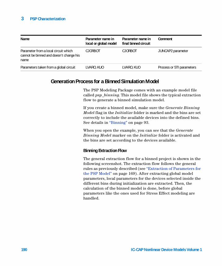
3 PSP Characterization
Generation Process for a Binned Simulation Model
Parameter from a local circuit which cannot be binned and doesn’t change his name
CJORBOT CJORBOT JUNCAP2 parameter
Parameters taken from a global circuit LVARO, KUO LVARO, KUO Process or STI parameters
Name Parameter name in local or global model
Parameter name in final binned circuit
Comment
190
The PSP Modeling Package comes with an example model file called psp_binning. This model file shows the typical extraction flow to generate a binned simulation model.
If you create a binned model, make sure the Generate Binning Model flag in the Initialize folder is marked and the bins are set correctly to include the available devices into the defined bins. See details in “Binning” on page 93.
When you open the example, you can see that the Generate Binning Model marker on the Initialize folder is activated and the bins are set according to the devices available.
Binning Extraction Flow
The general extraction flow for a binned project is shown in the following screenshot. The extraction flow follows the general rules as previously described (see “Extraction of Parameters for the PSP Model” on page 169). After extracting global model parameters, local parameters for the devices selected inside the different bins during initialization are extracted. Then, the calculation of the binned model is done, before global parameters like the ones used for Stress Effect modeling are handled.
IC-CAP Nonlinear Device Models Volume 1
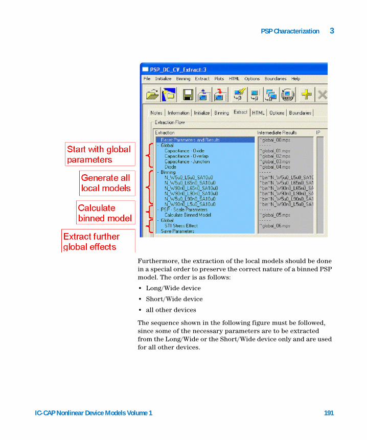
PSP Characterization 3
IC-CAP Nonlinear Device Models Vo
Furthermore, the extraction of the local models should be done in a special order to preserve the correct nature of a binned PSP model. The order is as follows:
• Long/Wide device
• Short/Wide device
• all other devices
The sequence shown in the following figure must be followed, since some of the necessary parameters are to be extracted from the Long/Wide or the Short/Wide device only and are used for all other devices.
lume 1 191
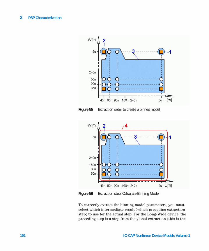
192
3 PSP Characterization
To correctly extract the binning model parameters, you must select which intermediate result (which preceding extraction step) to use for the actual step. For the Long/Wide device, the preceding step is a step from the global extraction (this is the
Figure 55 Extraction order to create a binned model
Figure 56 Extraction step: Calculate Binning Model
IC-CAP Nonlinear Device Models Volume 1
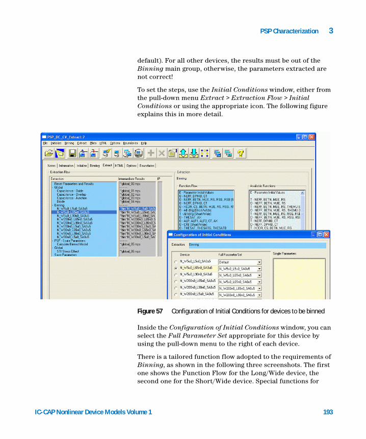
PSP Characterization 3
IC-CAP Nonlinear Device Models Vo
default). For all other devices, the results must be out of the Binning main group, otherwise, the parameters extracted are not correct!
To set the steps, use the Initial Conditions window, either from the pull-down menu Extract > Extraction Flow > Initial Conditions or using the appropriate icon. The following figure explains this in more detail.
Figure 57 Configuration of Initial Conditions for devices to be binned
Inside the Configuration of Initial Conditions window, you can select the Full Parameter Set appropriate for this device by using the pull-down menu to the right of each device.
There is a tailored function flow adopted to the requirements of Binning, as shown in the following three screenshots. The first one shows the Function Flow for the Long/Wide device, the second one for the Short/Wide device. Special functions for
lume 1 193
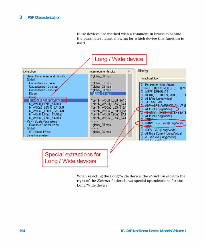
194
3 PSP Characterization
these devices are marked with a comment in brackets behind the parameter name, showing for which device this function is used.
When selecting the Long/Wide device, the Function Flow to the right of the Extract folder shows special optimizations for the Long/Wide device.
IC-CAP Nonlinear Device Models Volume 1
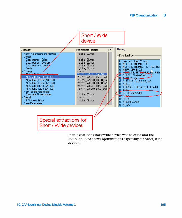
PSP Characterization 3
IC-CAP Nonlinear Device Models Vo
In this case, the Short/Wide device was selected and the Function Flow shows optimizations especially for Short/Wide devices.
lume 1 195
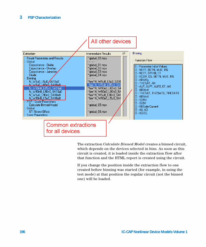
196
3 PSP Characterization
The extraction Calculate Binned Model creates a binned circuit, which depends on the devices selected in bins. As soon as this circuit is created, it is loaded inside the extraction flow after that function and the HTML report is created using the circuit.
If you change the position inside the extraction flow to one created before binning was started (for example, in using the test mode) at that position the regular circuit (not the binned one) will be loaded.
IC-CAP Nonlinear Device Models Volume 1
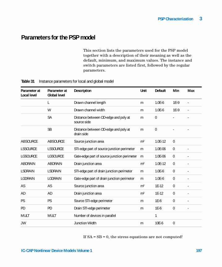
PSP Characterization 3
Parameters for the PSP model
IC-CAP Nonlinear Device Models Vo
This section lists the parameters used for the PSP model together with a description of their meaning as well as the default, minimum, and maximum values. The instance and switch parameters are listed first, followed by the regular parameters.
Table 31 Instance parameters for local and global model
Parameter at Local level
Parameter at Global level
Description Unit Default Min Max
L Drawn channel length m 1.0E-6 1E-9 -
W Drawn channel width m 1.0E-6 1E-9 -
SA Distance between OD-edge and poly at source side
m 0 - -
SB Distance between OD-edge and poly at drain side
m 0 - -
ABSOURCE ABSOURCE Source junction area m² 1.0E-12 0
LSSOURCE LSSOURCE STI-edge part of source junction perimeter m 1.0E-06 0 -
LGSOURCE LGSOURCE Gate-edge part of source junction perimeter m 1.0E-06 0 -
ABDRAIN ABDRAIN Drain junction area m² 1.0E-12 0 -
LSDRAIN LSDRAIN STI-edge part of drain junction perimeter m 1.0E-6 0 -
LGDRAIN LGDRAIN Gate-edge part of drain junction perimeter m 1.0E-6 0 -
AS AS Source junction area m² 1E-12 0 -
AD AD Drain junction area m² 1E-12 0 -
PS PS Source STI-edge perimeter m 1E-6 0 -
PD PD Drain STI-edge perimeter m 1E-6 0 -
MULT MULT Number of devices in parallel 1
JW Junction Width m 10E-6 0
If SA = SB = 0, the stress equations are not computed!
lume 1 197
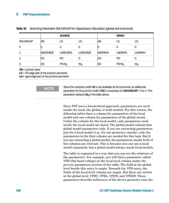
3 PSP Characterization
Table 32 Switching Parameter SWJUNCAP for Capacitance Calculation (global and local level)
SOURCE DRAIN
SWJUNCAP AB LS LG AB LS LG
0 0 0 0 0 0 0
1 ABSOURCE LSSOURCE LGSOURCE ABDRAIN LSDRAIN LGDRAIN
2 AS PS 0 AD PD 0
3 AS PS-WE WE AD PD-WE WE
AB = junction areaLS = STI-edge part of the junction perimeterLG = gate-edge part of the junction perimeter
NOTE Since the transistor width W is not available at the local level, an additional parameter for the junction width (JW) is necessary for SWJUNCAP = 3 or 4. This parameter replaces WE in the table above.
198
Since PSP uses a hierarchical approach, parameters are used inside the local, the global, or both models. For this reason, the following tables have a column for parameters of the local model and one column for parameters of the global model. Under the column for the local model, only parameters used inside the local model are listed. The global model column lists global model parameters only. If you are extracting parameters just for a local model (e.g., for one geometry exactly), only the parameters in the first column are needed for this task. But if you are extracting a global model, the parameters inside both of the columns are relevant. This is because you can use a local model separately, but a global model always needs local models.
The table is organized in a way that you can see the relations of the parameters. For example, you will find a parameter called VFB (flat band voltage) in the local level column under the process parameters section of the table. The field at the global level beside this entry is empty. Beneath the VFB entry, the fields of the local level column are empty. But there are entries at the global level: VFBO, VFBL, VFBW, and VFBLW. Those parameters describe influences of the device geometry onto the
IC-CAP Nonlinear Device Models Volume 1
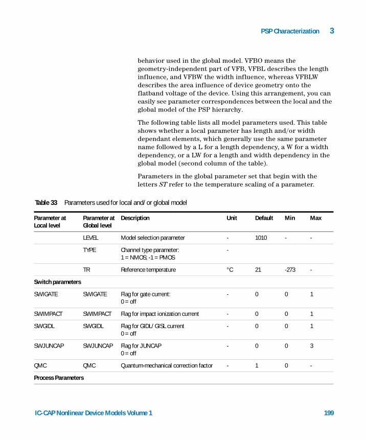
PSP Characterization 3
IC-CAP Nonlinear Device Models Vo
behavior used in the global model. VFBO means the geometry-independent part of VFB, VFBL describes the length influence, and VFBW the width influence, whereas VFBLW describes the area influence of device geometry onto the flatband voltage of the device. Using this arrangement, you can easily see parameter correspondences between the local and the global model of the PSP hierarchy.
The following table lists all model parameters used. This table shows whether a local parameter has length and/or width dependant elements, which generally use the same parameter name followed by a L for a length dependency, a W for a width dependency, or a LW for a length and width dependency in the global model (second column of the table).
Parameters in the global parameter set that begin with the letters ST refer to the temperature scaling of a parameter.
and/or global model
Table 33 Parameters used for local
Parameter atLocal level
Parameter at Global level
Description Unit Default Min Max
LEVEL Model selection parameter - 1010 - -
TYPE Channel type parameter:1 = NMOS; -1 = PMOS
-
TR Reference temperature °C 21 -273 -
Switch parameters
SWIGATE SWIGATE Flag for gate current:0 = off
- 0 0 1
SWIMPACT SWIMPACT Flag for impact ionization current - 0 0 1
SWGIDL SWGIDL Flag for GIDL/GISL current0 = off
- 0 0 1
SWJUNCAP SWJUNCAP Flag for JUNCAP0 = off
- 0 0 3
QMC QMC Quantum-mechanical correction factor - 1 0 -
Process Parameters
lume 1 199
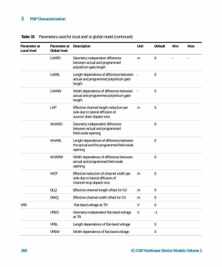
3 PSP Characterization
LVARO Geometry independent difference between actual and programmed polysilicon gate length
m 0 - -
LVARL Length dependence of difference between actual and programmed polysilicon gate length
- 0
LVARW Width dependence of difference between actual and programmed polysilicon gate length
- 0
LAP Effective channel length reduction per side due to lateral diffusion of source/drain dopant ions
m 0
WVARO Geometry independent difference between actual and programmed field-oxide opening
0
WVARL Length dependence of difference between the actual and the programmed field-oxide opening
0
WVARW Width dependence of difference between actual and programmed field oxide opening
0
WOT Effective reduction of channel width per side due to lateral diffusion of channel-stop dopant ions
m 0
DLQ Effective channel length offset for CV m 0
DWQ Effective channel width offset for CV m 0
VFB Flat-band voltage at TR V 0
VFBO Geometry-independent flat-band voltage at TR
V -1
VFBL Length dependence of flat-band voltage 0
VFBW Width dependence of flat-band voltage 0
Table 33 Parameters used for local and/or global model (continued)
Parameter atLocal level
Parameter at Global level
Description Unit Default Min Max
200 IC-CAP Nonlinear Device Models Volume 1
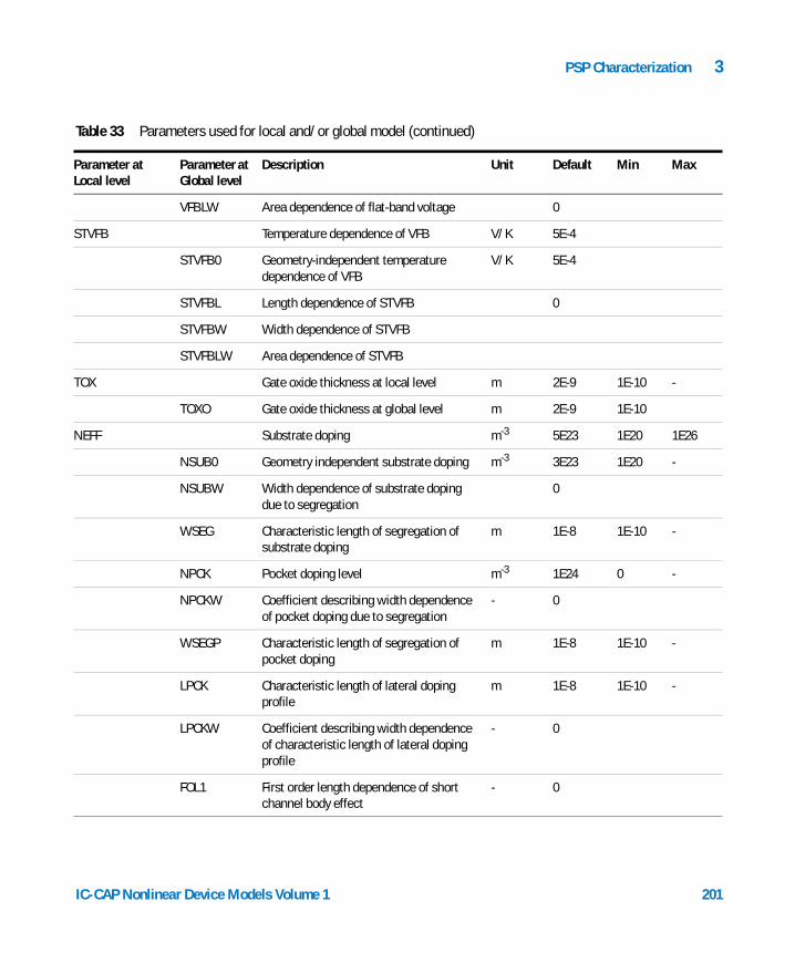
PSP Characterization 3
VFBLW Area dependence of flat-band voltage 0
STVFB Temperature dependence of VFB V/K 5E-4
STVFB0 Geometry-independent temperature dependence of VFB
V/K 5E-4
STVFBL Length dependence of STVFB 0
STVFBW Width dependence of STVFB
STVFBLW Area dependence of STVFB
TOX Gate oxide thickness at local level m 2E-9 1E-10 -
TOXO Gate oxide thickness at global level m 2E-9 1E-10
NEFF Substrate doping m-3 5E23 1E20 1E26
NSUB0 Geometry independent substrate doping m-3 3E23 1E20 -
NSUBW Width dependence of substrate doping due to segregation
0
WSEG Characteristic length of segregation of substrate doping
m 1E-8 1E-10 -
NPCK Pocket doping level m-3 1E24 0 -
NPCKW Coefficient describing width dependence of pocket doping due to segregation
- 0
WSEGP Characteristic length of segregation of pocket doping
m 1E-8 1E-10 -
LPCK Characteristic length of lateral doping profile
m 1E-8 1E-10 -
LPCKW Coefficient describing width dependence of characteristic length of lateral doping profile
- 0
FOL1 First order length dependence of short channel body effect
- 0
Table 33 Parameters used for local and/or global model (continued)
Parameter atLocal level
Parameter at Global level
Description Unit Default Min Max
IC-CAP Nonlinear Device Models Volume 1 201
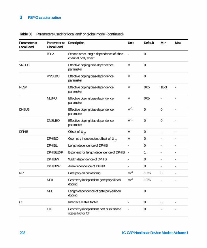
3 PSP Characterization
FOL2 Second order length dependence of short channel body effect
- 0
VNSUB Effective doping bias-dependence parameter
V 0
VNSUBO Effective doping bias-dependence parameter
V 0
NLSP Effective doping bias-dependence parameter
V 0.05 1E-3 -
NLSPO Effective doping bias-dependence parameter
V 0.05 - -
DNSUB Effective doping bias-dependence parameter
V--1 0 0 -
DNSUBO Effective doping bias-dependence parameter
V--1 0 0 -
DPHIB Offset of V 0 - -
DPHIBO Geometry independent offset of V 0 - -
DPHIBL Length dependence of DPHIB - 0 - -
DPHIBLEXP Exponent for length dependence of DPHIB - 1 - -
DPHIBW Width dependence of DPHIB - 0 - -
DPHIBLW Area dependence of DPHIB - 0 - -
NP Gate poly-silicon doping m-3 1E26 0 -
NP0 Geometry-independent gate polysilicon doping
m-3 1E26 - -
NPL Length dependence of gate poly-silicon doping
0
CT Interface states factor - 0 0 -
CT0 Geometry-independent part of interface states factor CT
- 0 - -
Table 33 Parameters used for local and/or global model (continued)
Parameter atLocal level
Parameter at Global level
Description Unit Default Min Max
ϕB
ϕB
202 IC-CAP Nonlinear Device Models Volume 1
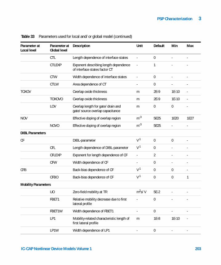
PSP Characterization 3
CTL Length dependence of interface states - 0 - -
CTLEXP Exponent describing length dependence of interface states factor CT
- 1 - -
CTW Width dependence of interface states - 0 - -
CTLW Area dependence of CT - 0 - -
TOXOV Overlap oxide thickness m 2E-9 1E-10 -
TOXOVO Overlap oxide thickness m 2E-9 1E-10 -
LOV Overlap length for gate/drain and gate/source overlap capacitance
m 0 0 -
NOV Effective doping of overlap region m-3 5E25 1E20 1E27
NOVO Effective doping of overlap region m-3 5E25 - -
DIBL Parameters
CF DIBL-parameter V-1 0 0 -
CFL Length dependence of DIBL-parameter V-1 0 - -
CFLEXP Exponent for length dependence of CF - 2 - -
CFW Width dependence of CF - 0 - -
CFB Back-bias dependence of CF V-1 0 0 -
CFBO Back-bias dependence of CF V-1 0 0 1
Mobility Parameters
UO Zero-field mobility at TR m2s/V 5E-2 - -
FBET1 Relative mobility decrease due to first lateral profile
- 0 - -
FBET1W Width dependence of FBET1 - 0 - -
LP1 Mobility-related characteristic length of first lateral profile
m 1E-8 1E-10 -
LP1W Width dependence of LP1 - 0 - -
Table 33 Parameters used for local and/or global model (continued)
Parameter atLocal level
Parameter at Global level
Description Unit Default Min Max
IC-CAP Nonlinear Device Models Volume 1 203
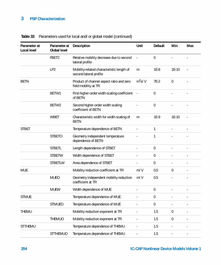
3 PSP Characterization
FBET2 Relative mobility decrease due to second lateral profile
- 0 - -
LP2 Mobility-related characteristic length of second lateral profile
m 1E-8 1E-10 -
BETN Product of channel aspect ratio and zero field mobility at TR
m2s/V 7E-2 0 -
BETW1 First higher-order width scaling coefficient of BETN
- 0 - -
BETW2 Second higher-order width scaling coefficient of BETN
- 0 - -
WBET Characteristic width for width scaling of BETN
m 1E-9 1E-10 -
STBET Temperature dependence of BETN - 1 - -
STBETO Geometry independent temperature dependence of BETN
- 1 - -
STBETL Length dependence of STBET - 0 - -
STBETW Width dependence of STBET - 0 - -
STBETLW Area dependence of STBET - 0 - -
MUE Mobility reduction coefficient at TR m/V 0.5 0 -
MUEO Geometry independent mobility reduction coefficient at TR
m/V 0.5 - -
MUEW Width dependence of MUE - 0 - -
STMUE Temperature dependence of MUE - 0 - -
STMUEO Temperature dependence of MUE - 0 - -
THEMU Mobility reduction exponent at TR - 1.5 0 -
THEMUO Mobility reduction exponent at TR - 1.5 0 -
STTHEMU Temperature dependence of THEMU - 1.5 - -
STTHEMUO Temperature dependence of THEMU - 1.5 - -
Table 33 Parameters used for local and/or global model (continued)
Parameter atLocal level
Parameter at Global level
Description Unit Default Min Max
204 IC-CAP Nonlinear Device Models Volume 1

PSP Characterization 3
CS Coulomb scattering parameter at TR - 0 0 -
CSO Geometry independent Coulomb scattering parameter at TR
- 0 - -
CSL Length dependence of CS - 0 - -
CSLEXP Exponent for length dependence of CS - 1 - -
CSW Width dependence of CS - 0 - -
CSLW Area dependence of CS - 0 - -
STCS Temperature dependence of CS - 0 - -
STCSO Temperature dependence of CS - 0 - -
XCOR Non-universality parameter V -1 0 0 -
XCORO Geometry independent non-universalityparameter
V -1 0 - -
XCORL Length dependence of XCOR - 0 - -
XCORW Width dependence of XCOR - 0 - -
XCORLW Area dependence of XCOR - 0 - -
STXCOR Temperature dependence of XCOR - 0 - -
STXCORO Temperature dependence of XCOR - 0 - -
FETA Effective field parameter - 1 0 -
FETAO Effective field parameter - 1 - -
Series Resistance Parameters
RS Source/drain series resistance at TR 30 0 -
RSW1 Source/drain series resistance for channel width WEN at TR
2500 - -
RSW2 Higher-order width scaling of source/drain series resistance
- 0 - -
STRS Temperature dependence of RS - 1 - -
Table 33 Parameters used for local and/or global model (continued)
Parameter atLocal level
Parameter at Global level
Description Unit Default Min Max
Ω
Ω
IC-CAP Nonlinear Device Models Volume 1 205
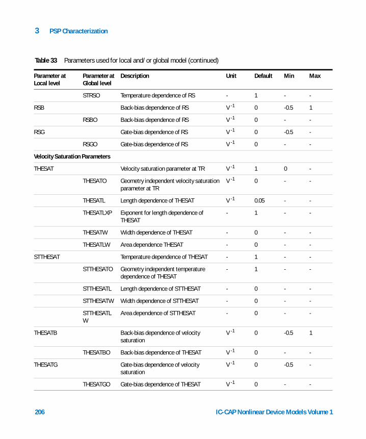
3 PSP Characterization
STRSO Temperature dependence of RS - 1 - -
RSB Back-bias dependence of RS V -1 0 -0.5 1
RSBO Back-bias dependence of RS V -1 0 - -
RSG Gate-bias dependence of RS V -1 0 -0.5 -
RSGO Gate-bias dependence of RS V -1 0 - -
Velocity Saturation Parameters
THESAT Velocity saturation parameter at TR V -1 1 0 -
THESATO Geometry independent velocity saturation parameter at TR
V -1 0 - -
THESATL Length dependence of THESAT V -1 0.05 - -
THESATLXP Exponent for length dependence of THESAT
- 1 - -
THESATW Width dependence of THESAT - 0 - -
THESATLW Area dependence THESAT - 0 - -
STTHESAT Temperature dependence of THESAT - 1 - -
STTHESATO Geometry independent temperature dependence of THESAT
- 1 - -
STTHESATL Length dependence of STTHESAT - 0 - -
STTHESATW Width dependence of STTHESAT - 0 - -
STTHESATLW
Area dependence of STTHESAT - 0 - -
THESATB Back-bias dependence of velocity saturation
V -1 0 -0.5 1
THESATBO Back-bias dependence of THESAT V -1 0 - -
THESATG Gate-bias dependence of velocity saturation
V -1 0 -0.5 -
THESATGO Gate-bias dependence of THESAT V -1 0 - -
Table 33 Parameters used for local and/or global model (continued)
Parameter atLocal level
Parameter at Global level
Description Unit Default Min Max
206 IC-CAP Nonlinear Device Models Volume 1
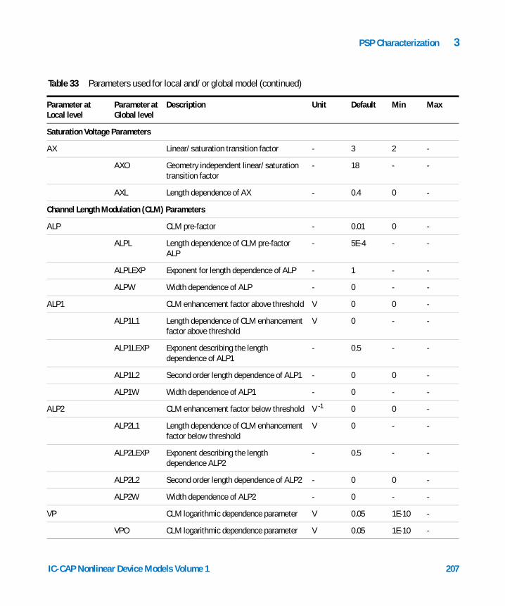
PSP Characterization 3
Saturation Voltage Parameters
AX Linear/saturation transition factor - 3 2 -
AXO Geometry independent linear/saturation transition factor
- 18 - -
AXL Length dependence of AX - 0.4 0 -
Channel Length Modulation (CLM) Parameters
ALP CLM pre-factor - 0.01 0 -
ALPL Length dependence of CLM pre-factor ALP
- 5E-4 - -
ALPLEXP Exponent for length dependence of ALP - 1 - -
ALPW Width dependence of ALP - 0 - -
ALP1 CLM enhancement factor above threshold V 0 0 -
ALP1L1 Length dependence of CLM enhancement factor above threshold
V 0 - -
ALP1LEXP Exponent describing the length dependence of ALP1
- 0.5 - -
ALP1L2 Second order length dependence of ALP1 - 0 0 -
ALP1W Width dependence of ALP1 - 0 - -
ALP2 CLM enhancement factor below threshold V -1 0 0 -
ALP2L1 Length dependence of CLM enhancement factor below threshold
V 0 - -
ALP2LEXP Exponent describing the length dependence ALP2
- 0.5 - -
ALP2L2 Second order length dependence of ALP2 - 0 0 -
ALP2W Width dependence of ALP2 - 0 - -
VP CLM logarithmic dependence parameter V 0.05 1E-10 -
VPO CLM logarithmic dependence parameter V 0.05 1E-10 -
Table 33 Parameters used for local and/or global model (continued)
Parameter atLocal level
Parameter at Global level
Description Unit Default Min Max
IC-CAP Nonlinear Device Models Volume 1 207
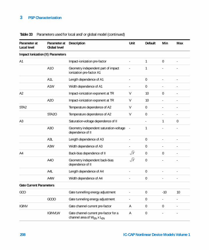
3 PSP Characterization
Impact Ionization (II) Parameters
A1 Impact-ionization pre-factor - 1 0 -
A1O Geometry independent part of impact ionization pre-factor A1
- 1 - -
A1L Length dependence of A1 - 0 - -
A1W Width dependence of A1 - 0 - -
A2 Impact-ionization exponent at TR V 10 0 -
A2O Impact-ionization exponent at TR V 10 - -
STA2 Temperature dependence of A2 V 0 - -
STA2O Temperature dependence of A2 V 0 - -
A3 Saturation-voltage dependence of II - 1 0
A3O Geometry independent saturation-voltage dependence of II
- 1 - -
A3L Length dependence of A3 - 0 - -
A3W Width dependence of A3 - 0 - -
A4 Back-bias dependence of II 0 0 -
A4O Geometry independent back-bias dependence of II
0 - -
A4L Length dependence of A4 - 0 - -
A4W Width dependence of A4 - 0 - -
Gate Current Parameters
GCO Gate tunnelling energy adjustment - 0 -10 10
GCOO Gate tunneling energy adjustment - 0 - -
IGINV Gate channel current pre-factor A 0 0 -
IGINVLW Gate channel current pre-factor for a channel area of WEN x LEN
A 0 - -
Table 33 Parameters used for local and/or global model (continued)
Parameter atLocal level
Parameter at Global level
Description Unit Default Min Max
V
V
208 IC-CAP Nonlinear Device Models Volume 1
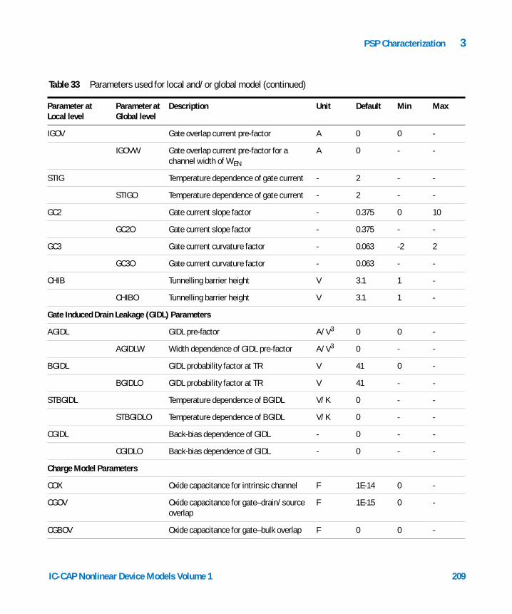
PSP Characterization 3
IGOV Gate overlap current pre-factor A 0 0 -
IGOVW Gate overlap current pre-factor for a channel width of WEN
A 0 - -
STIG Temperature dependence of gate current - 2 - -
STIGO Temperature dependence of gate current - 2 - -
GC2 Gate current slope factor - 0.375 0 10
GC2O Gate current slope factor - 0.375 - -
GC3 Gate current curvature factor - 0.063 -2 2
GC3O Gate current curvature factor - 0.063 - -
CHIB Tunnelling barrier height V 3.1 1 -
CHIBO Tunnelling barrier height V 3.1 1 -
Gate Induced Drain Leakage (GIDL) Parameters
AGIDL GIDL pre-factor A/V3 0 0 -
AGIDLW Width dependence of GIDL pre-factor A/V3 0 - -
BGIDL GIDL probability factor at TR V 41 0 -
BGIDLO GIDL probability factor at TR V 41 - -
STBGIDL Temperature dependence of BGIDL V/K 0 - -
STBGIDLO Temperature dependence of BGIDL V/K 0 - -
CGIDL Back-bias dependence of GIDL - 0 - -
CGIDLO Back-bias dependence of GIDL - 0 - -
Charge Model Parameters
COX Oxide capacitance for intrinsic channel F 1E-14 0 -
CGOV Oxide capacitance for gate–drain/source overlap
F 1E-15 0 -
CGBOV Oxide capacitance for gate–bulk overlap F 0 0 -
Table 33 Parameters used for local and/or global model (continued)
Parameter atLocal level
Parameter at Global level
Description Unit Default Min Max
IC-CAP Nonlinear Device Models Volume 1 209
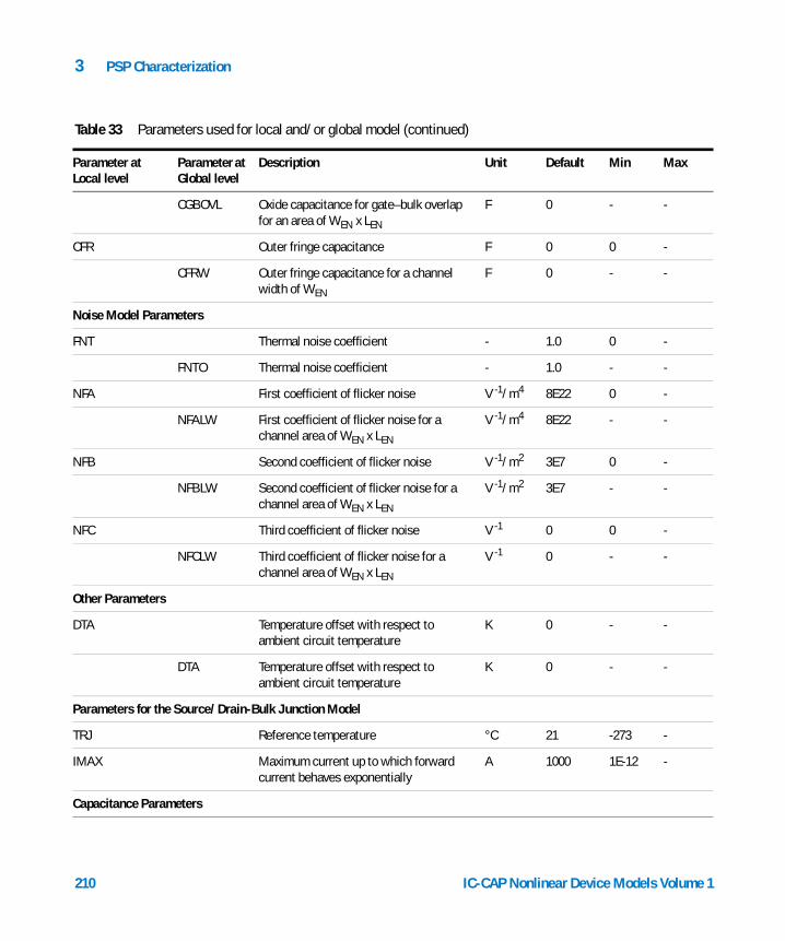
3 PSP Characterization
CGBOVL Oxide capacitance for gate–bulk overlapfor an area of WEN x LEN
F 0 - -
CFR Outer fringe capacitance F 0 0 -
CFRW Outer fringe capacitance for a channel width of WEN
F 0 - -
Noise Model Parameters
FNT Thermal noise coefficient - 1.0 0 -
FNTO Thermal noise coefficient - 1.0 - -
NFA First coefficient of flicker noise V -1/m4 8E22 0 -
NFALW First coefficient of flicker noise for a channel area of WEN x LEN
V -1/m4 8E22 - -
NFB Second coefficient of flicker noise V -1/m2 3E7 0 -
NFBLW Second coefficient of flicker noise for a channel area of WEN x LEN
V -1/m2 3E7 - -
NFC Third coefficient of flicker noise V -1 0 0 -
NFCLW Third coefficient of flicker noise for a channel area of WEN x LEN
V -1 0 - -
Other Parameters
DTA Temperature offset with respect to ambient circuit temperature
K 0 - -
DTA Temperature offset with respect to ambient circuit temperature
K 0 - -
Parameters for the Source/Drain-Bulk Junction Model
TRJ Reference temperature °C 21 -273 -
IMAX Maximum current up to which forward current behaves exponentially
A 1000 1E-12 -
Capacitance Parameters
Table 33 Parameters used for local and/or global model (continued)
Parameter atLocal level
Parameter at Global level
Description Unit Default Min Max
210 IC-CAP Nonlinear Device Models Volume 1
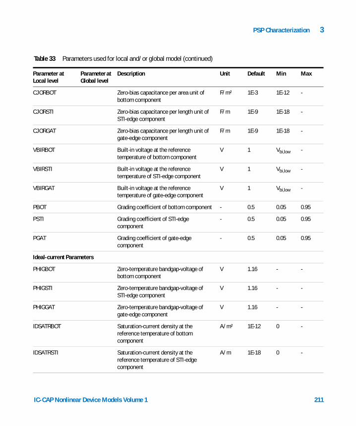
PSP Characterization 3
CJORBOT Zero-bias capacitance per area unit of bottom component
F/m² 1E-3 1E-12 -
CJORSTI Zero-bias capacitance per length unit of STI-edge component
F/m 1E-9 1E-18 -
CJORGAT Zero-bias capacitance per length unit of gate-edge component
F/m 1E-9 1E-18 -
VBIRBOT Built-in voltage at the reference temperature of bottom component
V 1 Vbi,low -
VBIRSTI Built-in voltage at the reference temperature of STI-edge component
V 1 Vbi,low -
VBIRGAT Built-in voltage at the reference temperature of gate-edge component
V 1 Vbi,low -
PBOT Grading coefficient of bottom component - 0.5 0.05 0.95
PSTI Grading coefficient of STI-edge component
- 0.5 0.05 0.95
PGAT Grading coefficient of gate-edge component
- 0.5 0.05 0.95
Ideal-current Parameters
PHIGBOT Zero-temperature bandgap-voltage of bottom component
V 1.16 - -
PHIGSTI Zero-temperature bandgap-voltage of STI-edge component
V 1.16 - -
PHIGGAT Zero-temperature bandgap-voltage of gate-edge component
V 1.16 - -
IDSATRBOT Saturation-current density at the reference temperature of bottom component
A/m² 1E-12 0 -
IDSATRSTI Saturation-current density at the reference temperature of STI-edge component
A/m 1E-18 0 -
Table 33 Parameters used for local and/or global model (continued)
Parameter atLocal level
Parameter at Global level
Description Unit Default Min Max
IC-CAP Nonlinear Device Models Volume 1 211
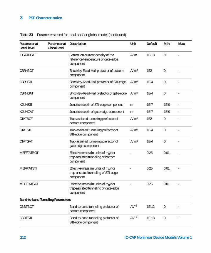
3 PSP Characterization
IDSATRGAT Saturation-current density at the reference temperature of gate-edge component
A/m 1E-18 0 -
CSRHBOT Shockley-Read-Hall prefactor of bottom component
A/m³ 1E2 0 -
CSRHSTI Shockley-Read-Hall prefactor of STI-edge component
A/m² 1E-4 0 -
CSRHGAT Shockley-Read-Hall prefactor of gate-edge component
A/m² 1E-4 0 -
XJUNSTI Junction depth of STI-edge component m 1E-7 1E-9 -
XJUNGAT Junction depth of gate-edge component m 1E-7 1E-9 -
CTATBOT Trap-assisted tunneling prefactor of bottom component
A/m³ 1E2 0 -
CTATSTI Trap-assisted tunneling prefactor of STI-edge component
A/m² 1E-4 0 -
CTATGAT Trap-assisted tunneling prefactor of gate-edge component
A/m² 1E-4 0 -
MEFFTATBOT Effective mass (in units of m0) for trap-assisted tunneling of bottom component
- 0.25 0.01 -
MEFFTATSTI Effective mass (in units of m0) for trap-assisted tunneling of STI-edge component
- 0.25 0.01 -
MEFFTATGAT Effective mass (in units of m0) for trap-assisted tunneling of gate-edge component
- 0.25 0.01 -
Band-to-band Tunneling Parameters
CBBTBOT Band-to-band tunneling prefactor of bottom component
AV -3 1E-12 0 -
CBBTSTI Band-to-band tunneling prefactor of STI-edge component
AV -3 1E-18 0 -
Table 33 Parameters used for local and/or global model (continued)
Parameter atLocal level
Parameter at Global level
Description Unit Default Min Max
212 IC-CAP Nonlinear Device Models Volume 1
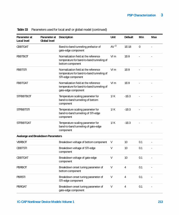
PSP Characterization 3
CBBTGAT Band-to-band tunneling prefactor of gate-edge component
AV -3 1E-18 0 -
FBBTBOT Normalization field at the reference temperature for band-to-band tunneling of bottom component
V/m 1E-9 - -
FBBTSTI Normalization field at the reference temperature for band-to-band tunneling of STI-edge component
V/m 1E-9 - -
FBBTGAT Normalization field at the reference temperature for band-to-band tunneling of gate-edge component
V/m 1E-9 - -
STFBBTBOT Temperature scaling parameter for band-to-band tunneling of bottom component
1/K -1E-3 - -
STFBBTSTI Temperature scaling parameter for band-to-band tunneling of STI-edge component
1/K -1E-3 - -
STFBBTGAT Temperature scaling parameter for band-to-band tunneling of gate-edge component
1/K -1E-3 - -
Avalange and Breakdown Parameters
VBRBOT Breakdown voltage of bottom component V 10 0.1 -
CBBTSTI Breakdown voltage of STI-edge component
V 10 0.1 -
CBBTGAT Breakdown voltage of gate-edge component
V 10 0.1 -
PBRBOT Breakdown onset tuning parameter of bottom component
V 4 0.1 -
PBRSTI Breakdown onset tuning parameter of STI-edge component
V 4 0.1 -
PBRGAT Breakdown onset tuning parameter of gate-edge component
V 4 0.1 -
Table 33 Parameters used for local and/or global model (continued)
Parameter atLocal level
Parameter at Global level
Description Unit Default Min Max
IC-CAP Nonlinear Device Models Volume 1 213
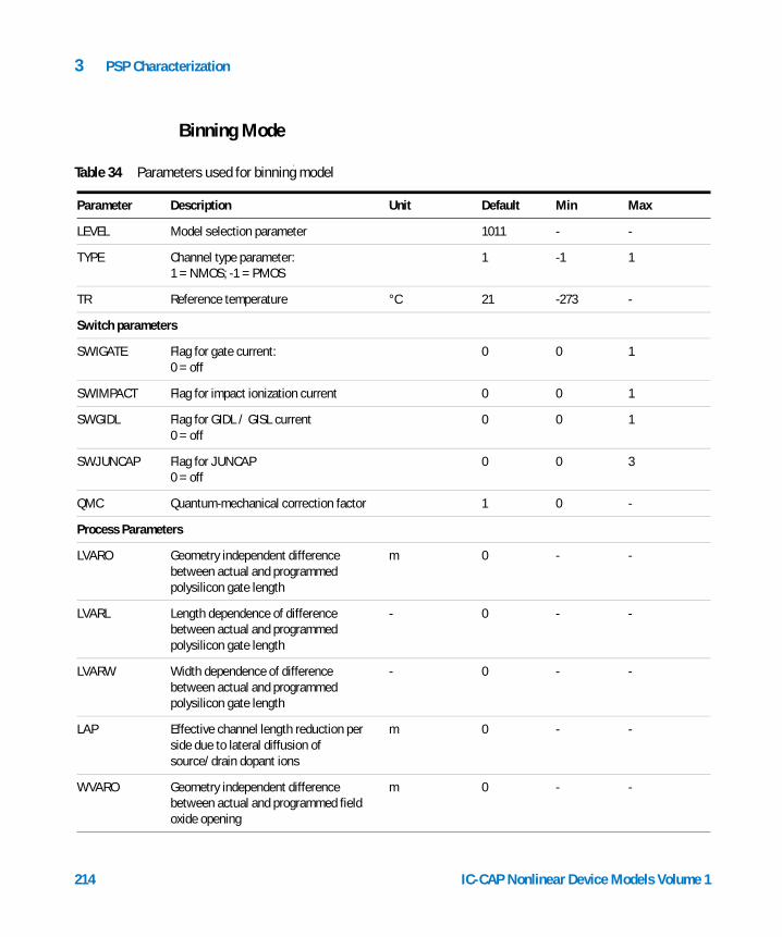
3 PSP Characterization
Binning Mode
214
l
ng model
Table 34 Parameters used for binni
Parameter Description Unit Default Min Max
LEVEL Model selection parameter 1011 - -
TYPE Channel type parameter:1 = NMOS; -1 = PMOS
1 -1 1
TR Reference temperature °C 21 -273 -
Switch parameters
SWIGATE Flag for gate current:0 = off
0 0 1
SWIMPACT Flag for impact ionization current 0 0 1
SWGIDL Flag for GIDL / GISL current0 = off
0 0 1
SWJUNCAP Flag for JUNCAP0 = off
0 0 3
QMC Quantum-mechanical correction factor 1 0 -
Process Parameters
LVARO Geometry independent difference between actual and programmed polysilicon gate length
m 0 - -
LVARL Length dependence of difference between actual and programmed polysilicon gate length
- 0 - -
LVARW Width dependence of difference between actual and programmed polysilicon gate length
- 0 - -
LAP Effective channel length reduction per side due to lateral diffusion of source/drain dopant ions
m 0 - -
WVARO Geometry independent difference between actual and programmed field oxide opening
m 0 - -
IC-CAP Nonlinear Device Models Volume 1
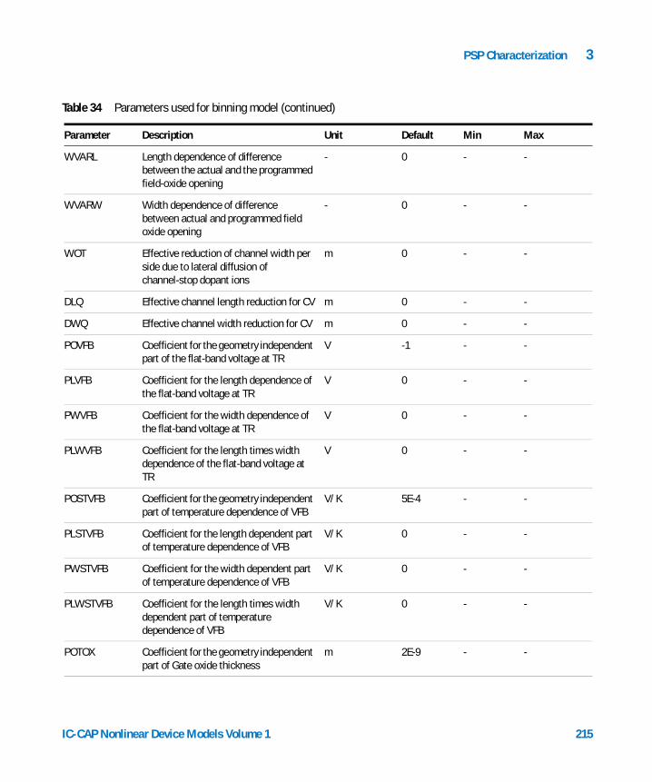
PSP Characterization 3
WVARL Length dependence of difference between the actual and the programmed field-oxide opening
- 0 - -
WVARW Width dependence of difference between actual and programmed field oxide opening
- 0 - -
WOT Effective reduction of channel width per side due to lateral diffusion of channel-stop dopant ions
m 0 - -
DLQ Effective channel length reduction for CV m 0 - -
DWQ Effective channel width reduction for CV m 0 - -
POVFB Coefficient for the geometry independent part of the flat-band voltage at TR
V -1 - -
PLVFB Coefficient for the length dependence of the flat-band voltage at TR
V 0 - -
PWVFB Coefficient for the width dependence of the flat-band voltage at TR
V 0 - -
PLWVFB Coefficient for the length times width dependence of the flat-band voltage at TR
V 0 - -
POSTVFB Coefficient for the geometry independent part of temperature dependence of VFB
V/K 5E-4 - -
PLSTVFB Coefficient for the length dependent part of temperature dependence of VFB
V/K 0 - -
PWSTVFB Coefficient for the width dependent part of temperature dependence of VFB
V/K 0 - -
PLWSTVFB Coefficient for the length times width dependent part of temperature dependence of VFB
V/K 0 - -
POTOX Coefficient for the geometry independent part of Gate oxide thickness
m 2E-9 - -
Table 34 Parameters used for binning model (continued)
Parameter Description Unit Default Min Max
IC-CAP Nonlinear Device Models Volume 1 215
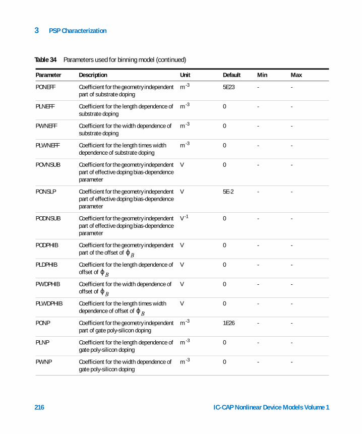
3 PSP Characterization
PONEFF Coefficient for the geometry independent part of substrate doping
m -3 5E23 - -
PLNEFF Coefficient for the length dependence of substrate doping
m -3 0 - -
PWNEFF Coefficient for the width dependence of substrate doping
m -3 0 - -
PLWNEFF Coefficient for the length times width dependence of substrate doping
m -3 0 - -
POVNSUB Coefficient for the geometry independent part of effective doping bias-dependence parameter
V 0 - -
PONSLP Coefficient for the geometry independent part of effective doping bias-dependence parameter
V 5E-2 - -
PODNSUB Coefficient for the geometry independent part of effective doping bias-dependence parameter
V -1 0 - -
PODPHIB Coefficient for the geometry independent part of the offset of
V 0 - -
PLDPHIB Coefficient for the length dependence of offset of
V 0 - -
PWDPHIB Coefficient for the width dependence of offset of
V 0 - -
PLWDPHIB Coefficient for the length times width dependence of offset of
V 0 - -
PONP Coefficient for the geometry independent part of gate poly-silicon doping
m -3 1E26 - -
PLNP Coefficient for the length dependence of gate poly-silicon doping
m -3 0 - -
PWNP Coefficient for the width dependence of gate poly-silicon doping
m -3 0 - -
Table 34 Parameters used for binning model (continued)
Parameter Description Unit Default Min Max
ϕB
ϕB
ϕB
ϕB
216 IC-CAP Nonlinear Device Models Volume 1
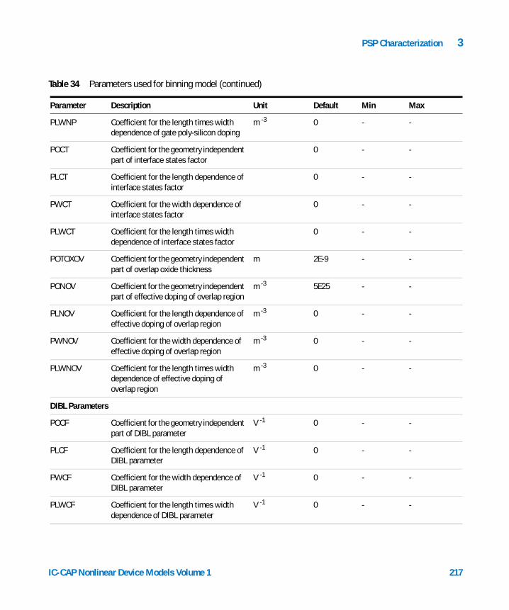
PSP Characterization 3
PLWNP Coefficient for the length times width dependence of gate poly-silicon doping
m -3 0 - -
POCT Coefficient for the geometry independent part of interface states factor
0 - -
PLCT Coefficient for the length dependence of interface states factor
0 - -
PWCT Coefficient for the width dependence of interface states factor
0 - -
PLWCT Coefficient for the length times width dependence of interface states factor
0 - -
POTOXOV Coefficient for the geometry independent part of overlap oxide thickness
m 2E-9 - -
PONOV Coefficient for the geometry independent part of effective doping of overlap region
m -3 5E25 - -
PLNOV Coefficient for the length dependence of effective doping of overlap region
m -3 0 - -
PWNOV Coefficient for the width dependence of effective doping of overlap region
m -3 0 - -
PLWNOV Coefficient for the length times width dependence of effective doping of overlap region
m -3 0 - -
DIBL Parameters
POCF Coefficient for the geometry independent part of DIBL parameter
V -1 0 - -
PLCF Coefficient for the length dependence of DIBL parameter
V -1 0 - -
PWCF Coefficient for the width dependence of DIBL parameter
V -1 0 - -
PLWCF Coefficient for the length times width dependence of DIBL parameter
V -1 0 - -
Table 34 Parameters used for binning model (continued)
Parameter Description Unit Default Min Max
IC-CAP Nonlinear Device Models Volume 1 217
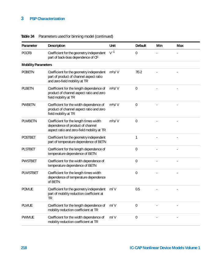
3 PSP Characterization
POCFB Coefficient for the geometry independent part of back-bias dependence of CF
V -1 0 - -
Mobility Parameters
POBETN Coefficient for the geometry independent part of product of channel aspect ratio and zero-field mobility at TR
m²s/V 7E-2 - -
PLBETN Coefficient for the length dependence of product of channel aspect ratio and zero field mobility at TR
m²s/V 0 - -
PWBETN Coefficient for the width dependence of product of channel aspect ratio and zero field mobility at TR
m²s/V 0 - -
PLWBETN Coefficient for the length times width dependence of product of channel aspect ratio and zero-field mobility at TR
m²s/V 0 - -
POSTBET Coefficient for the geometry independent part of temperature dependence of BETN
1 - -
PLSTBET Coefficient for the length dependence of temperature dependence of BETN
0 - -
PWSTBET Coefficient for the width dependence of temperature dependence of BETN
0 - -
PLWSTBET Coefficient for the length times width dependence of temperature dependence of BETN
0 - -
POMUE Coefficient for the geometry independent part of mobility reduction coefficient at TR
m/V 0.5 - -
PLMUE Coefficient for the length dependence of mobility reduction coefficient at TR
m/V 0 - -
PWMUE Coefficient for the width dependence of mobility reduction coefficient at TR
m/V 0 - -
Table 34 Parameters used for binning model (continued)
Parameter Description Unit Default Min Max
218 IC-CAP Nonlinear Device Models Volume 1

PSP Characterization 3
PLWMUE Coefficient for the length times width dependence of mobility reduction coefficient at TR
m/V 0 - -
POSTMUE Coefficient for the geometry independent part of temperature dependence of MUE
0 - -
POTHEMU Coefficient for the geometry independent part of mobility reduction exponent at TR
1.5 - -
POSTTHEMU Coefficient for the geometry independent part of temperature dependence of THEMU
1.5 - -
POCS Coefficient for the geometry independent part of Coulomb scattering parameter at TR
0 - -
PLCS Coefficient for the length dependence of Coulomb scattering parameter at TR
0 - -
PWCS Coefficient for the width dependence of Coulomb scattering parameter at TR
0 - -
PLWCS Coefficient for the length times width dependence of Coulomb scattering parameter at TR
0 - -
POSTCS Coefficient for the geometry independent part of temperature dependence of CS
0 - -
POXCOR Coefficient for the geometry independent part of non-universality parameter
V -1 0 - -
PLXCOR Coefficient for the length dependence of non-universality parameter
V -1 0 - -
PWXCOR Coefficient for the width dependence of non-universality parameter
V -1 0 - -
PLWXCOR Coefficient for the length times width dependence of non-universality parameter
V -1 0 - -
POSTXCOR Coefficient for the geometry independent part of temperature dependence of XCOR
0 - -
Table 34 Parameters used for binning model (continued)
Parameter Description Unit Default Min Max
IC-CAP Nonlinear Device Models Volume 1 219
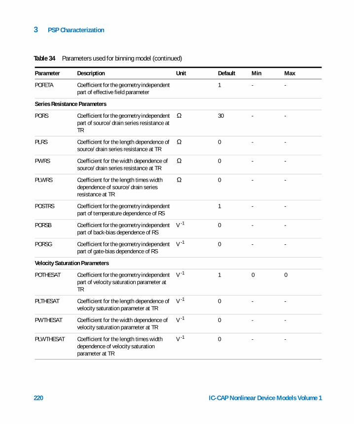
3 PSP Characterization
POFETA Coefficient for the geometry independent part of effective field parameter
1 - -
Series Resistance Parameters
PORS Coefficient for the geometry independent part of source/drain series resistance at TR
30 - -
PLRS Coefficient for the length dependence of source/drain series resistance at TR
0 - -
PWRS Coefficient for the width dependence of source/drain series resistance at TR
0 - -
PLWRS Coefficient for the length times width dependence of source/drain series resistance at TR
0 - -
POSTRS Coefficient for the geometry independent part of temperature dependence of RS
1 - -
PORSB Coefficient for the geometry independent part of back-bias dependence of RS
V -1 0 - -
PORSG Coefficient for the geometry independent part of gate-bias dependence of RS
V -1 0 - -
Velocity Saturation Parameters
POTHESAT Coefficient for the geometry independent part of velocity saturation parameter at TR
V -1 1 0 0
PLTHESAT Coefficient for the length dependence of velocity saturation parameter at TR
V -1 0 - -
PWTHESAT Coefficient for the width dependence of velocity saturation parameter at TR
V -1 0 - -
PLWTHESAT Coefficient for the length times width dependence of velocity saturation parameter at TR
V -1 0 - -
Table 34 Parameters used for binning model (continued)
Parameter Description Unit Default Min Max
Ω
Ω
Ω
Ω
220 IC-CAP Nonlinear Device Models Volume 1
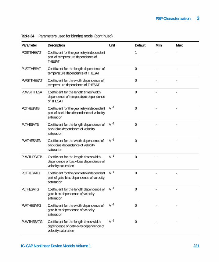
PSP Characterization 3
POSTTHESAT Coefficient for the geometry independent part of temperature dependence of THESAT
1 - -
PLSTTHESAT Coefficient for the length dependence of temperature dependence of THESAT
0 - -
PWSTTHESAT Coefficient for the width dependence of temperature dependence of THESAT
0 - -
PLWSTTHESAT Coefficient for the length times width dependence of temperature dependence of THESAT
0 - -
POTHESATB Coefficient for the geometry independent part of back-bias dependence of velocity saturation
V -1 0 - -
PLTHESATB Coefficient for the length dependence of back-bias dependence of velocity saturation
V -1 0 - -
PWTHESATB Coefficient for the width dependence of back-bias dependence of velocity saturation
V -1 0 - -
PLWTHESATB Coefficient for the length times width dependence of back-bias dependence of velocity saturation
V -1 0 - -
POTHESATG Coefficient for the geometry independent part of gate-bias dependence of velocity saturation
V -1 0 - -
PLTHESATG Coefficient for the length dependence of gate-bias dependence of velocity saturation
V -1 0 - -
PWTHESATG Coefficient for the width dependence of gate-bias dependence of velocity saturation
V -1 0 - -
PLWTHESATG Coefficient for the length times width dependence of gate-bias dependence of velocity saturation
V -1 0 - -
Table 34 Parameters used for binning model (continued)
Parameter Description Unit Default Min Max
IC-CAP Nonlinear Device Models Volume 1 221
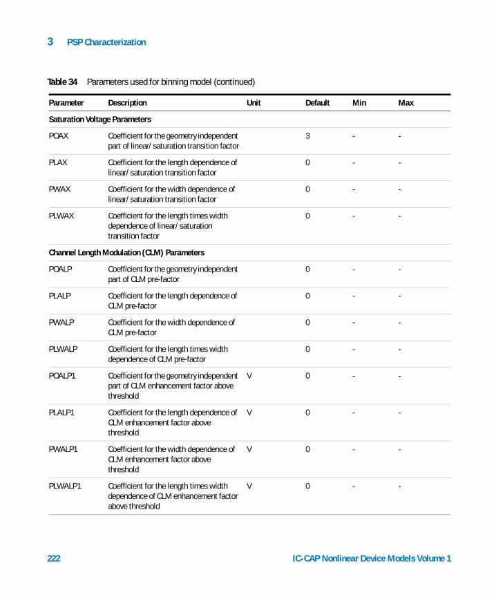
3 PSP Characterization
Saturation Voltage Parameters
POAX Coefficient for the geometry independent part of linear/saturation transition factor
3 - -
PLAX Coefficient for the length dependence of linear/saturation transition factor
0 - -
PWAX Coefficient for the width dependence of linear/saturation transition factor
0 - -
PLWAX Coefficient for the length times width dependence of linear/saturation transition factor
0 - -
Channel Length Modulation (CLM) Parameters
POALP Coefficient for the geometry independent part of CLM pre-factor
0 - -
PLALP Coefficient for the length dependence of CLM pre-factor
0 - -
PWALP Coefficient for the width dependence of CLM pre-factor
0 - -
PLWALP Coefficient for the length times width dependence of CLM pre-factor
0 - -
POALP1 Coefficient for the geometry independent part of CLM enhancement factor above threshold
V 0 - -
PLALP1 Coefficient for the length dependence of CLM enhancement factor above threshold
V 0 - -
PWALP1 Coefficient for the width dependence of CLM enhancement factor above threshold
V 0 - -
PLWALP1 Coefficient for the length times width dependence of CLM enhancement factor above threshold
V 0 - -
Table 34 Parameters used for binning model (continued)
Parameter Description Unit Default Min Max
222 IC-CAP Nonlinear Device Models Volume 1
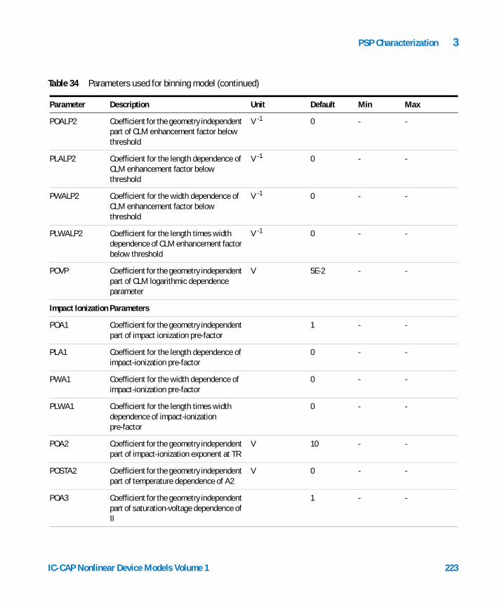
PSP Characterization 3
POALP2 Coefficient for the geometry independent part of CLM enhancement factor below threshold
V -1 0 - -
PLALP2 Coefficient for the length dependence of CLM enhancement factor below threshold
V -1 0 - -
PWALP2 Coefficient for the width dependence of CLM enhancement factor below threshold
V -1 0 - -
PLWALP2 Coefficient for the length times width dependence of CLM enhancement factor below threshold
V -1 0 - -
POVP Coefficient for the geometry independent part of CLM logarithmic dependence parameter
V 5E-2 - -
Impact Ionization Parameters
POA1 Coefficient for the geometry independent part of impact ionization pre-factor
1 - -
PLA1 Coefficient for the length dependence of impact-ionization pre-factor
0 - -
PWA1 Coefficient for the width dependence of impact-ionization pre-factor
0 - -
PLWA1 Coefficient for the length times width dependence of impact-ionization pre-factor
0 - -
POA2 Coefficient for the geometry independent part of impact-ionization exponent at TR
V 10 - -
POSTA2 Coefficient for the geometry independent part of temperature dependence of A2
V 0 - -
POA3 Coefficient for the geometry independent part of saturation-voltage dependence of II
1 - -
Table 34 Parameters used for binning model (continued)
Parameter Description Unit Default Min Max
IC-CAP Nonlinear Device Models Volume 1 223
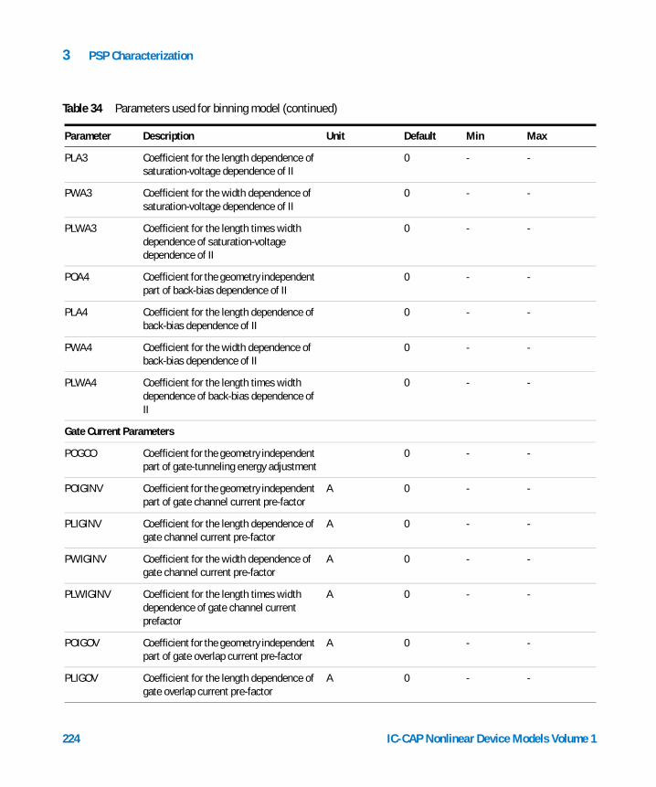
3 PSP Characterization
PLA3 Coefficient for the length dependence of saturation-voltage dependence of II
0 - -
PWA3 Coefficient for the width dependence of saturation-voltage dependence of II
0 - -
PLWA3 Coefficient for the length times width dependence of saturation-voltage dependence of II
0 - -
POA4 Coefficient for the geometry independent part of back-bias dependence of II
0 - -
PLA4 Coefficient for the length dependence of back-bias dependence of II
0 - -
PWA4 Coefficient for the width dependence of back-bias dependence of II
0 - -
PLWA4 Coefficient for the length times width dependence of back-bias dependence of II
0 - -
Gate Current Parameters
POGCO Coefficient for the geometry independent part of gate-tunneling energy adjustment
0 - -
POIGINV Coefficient for the geometry independent part of gate channel current pre-factor
A 0 - -
PLIGINV Coefficient for the length dependence of gate channel current pre-factor
A 0 - -
PWIGINV Coefficient for the width dependence of gate channel current pre-factor
A 0 - -
PLWIGINV Coefficient for the length times width dependence of gate channel current prefactor
A 0 - -
POIGOV Coefficient for the geometry independent part of gate overlap current pre-factor
A 0 - -
PLIGOV Coefficient for the length dependence of gate overlap current pre-factor
A 0 - -
Table 34 Parameters used for binning model (continued)
Parameter Description Unit Default Min Max
224 IC-CAP Nonlinear Device Models Volume 1
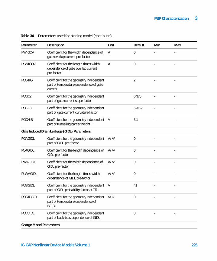
PSP Characterization 3
PWIGOV Coefficient for the width dependence of gate overlap current pre-factor
A 0 - -
PLWIGOV Coefficient for the length times width dependence of gate overlap current pre-factor
A 0 - -
POSTIG Coefficient for the geometry independent part of temperature dependence of gate current
2 - -
POGC2 Coefficient for the geometry independent part of gate current slope factor
0.375 - -
POGC3 Coefficient for the geometry independent part of gate current curvature factor
6.3E-2 - -
POCHIB Coefficient for the geometry independent part of tunneling barrier height
V 3.1 - -
Gate Induced Drain Leakage (GIDL) Parameters
POAGIDL Coefficient for the geometry independent part of GIDL pre-factor
A/V³ 0 - -
PLAGIDL Coefficient for the length dependence of GIDL pre-factor
A/V³ 0 - -
PWAGIDL Coefficient for the width dependence of GIDL pre-factor
A/V³ 0 - -
PLWAGIDL Coefficient for the length times width dependence of GIDL pre-factor
A/V³ 0 - -
POBGIDL Coefficient for the geometry independent part of GIDL probability factor at TR
V 41 - -
POSTBGIDL Coefficient for the geometry independent part of temperature dependence of BGIDL
V/K 0 - -
POCGIDL Coefficient for the geometry independent part of back-bias dependence of GIDL
0 - -
Charge Model Parameters
Table 34 Parameters used for binning model (continued)
Parameter Description Unit Default Min Max
IC-CAP Nonlinear Device Models Volume 1 225
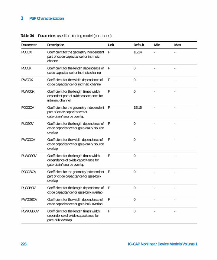
3 PSP Characterization
POCOX Coefficient for the geometry independent part of oxide capacitance for intrinsic channel
F 1E-14 - -
PLCOX Coefficient for the length dependence of oxide capacitance for intrinsic channel
F 0 - -
PWCOX Coefficient for the width dependence of oxide capacitance for intrinsic channel
F 0 - -
PLWCOX Coefficient for the length times width dependent part of oxide capacitance for intrinsic channel
F 0 - -
POCGOV Coefficient for the geometry independent part of oxide capacitance for gate-drain/source overlap
F 1E-15 - -
PLCGOV Coefficient for the length dependence of oxide capacitance for gate-drain/source overlap
F 0 - -
PWCGOV Coefficient for the width dependence of oxide capacitance for gate-drain/source overlap
F 0 - -
PLWCGOV Coefficient for the length times width dependence of oxide capacitance for gate-drain/source overlap
F 0 - -
POCGBOV Coefficient for the geometry independent part of oxide capacitance for gate-bulk overlap
F 0 - -
PLCGBOV Coefficient for the length dependence of oxide capacitance for gate-bulk overlap
F 0 - -
PWCGBOV Coefficient for the width dependence of oxide capacitance for gate-bulk overlap
F 0 - -
PLWCGBOV Coefficient for the length times width dependence of oxide capacitance for gate-bulk overlap
F 0 - -
Table 34 Parameters used for binning model (continued)
Parameter Description Unit Default Min Max
226 IC-CAP Nonlinear Device Models Volume 1
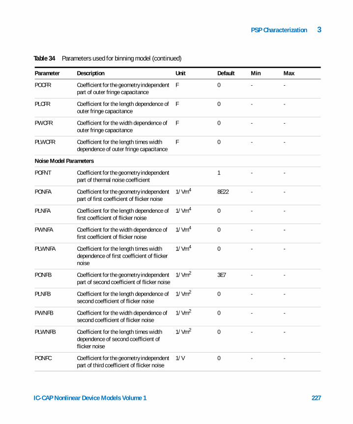
PSP Characterization 3
POCFR Coefficient for the geometry independent part of outer fringe capacitance
F 0 - -
PLCFR Coefficient for the length dependence of outer fringe capacitance
F 0 - -
PWCFR Coefficient for the width dependence of outer fringe capacitance
F 0 - -
PLWCFR Coefficient for the length times width dependence of outer fringe capacitance
F 0 - -
Noise Model Parameters
POFNT Coefficient for the geometry independent part of thermal noise coefficient
1 - -
PONFA Coefficient for the geometry independent part of first coefficient of flicker noise
1/Vm4 8E22 - -
PLNFA Coefficient for the length dependence of first coefficient of flicker noise
1/Vm4 0 - -
PWNFA Coefficient for the width dependence of first coefficient of flicker noise
1/Vm4 0 - -
PLWNFA Coefficient for the length times width dependence of first coefficient of flicker noise
1/Vm4 0 - -
PONFB Coefficient for the geometry independent part of second coefficient of flicker noise
1/Vm2 3E7 - -
PLNFB Coefficient for the length dependence of second coefficient of flicker noise
1/Vm2 0 - -
PWNFB Coefficient for the width dependence of second coefficient of flicker noise
1/Vm2 0 - -
PLWNFB Coefficient for the length times width dependence of second coefficient of flicker noise
1/Vm2 0 - -
PONFC Coefficient for the geometry independent part of third coefficient of flicker noise
1/V 0 - -
Table 34 Parameters used for binning model (continued)
Parameter Description Unit Default Min Max
IC-CAP Nonlinear Device Models Volume 1 227

3 PSP Characterization
Stress Model
PLNFC Coefficient for the length dependence of third coefficient of flicker noise
1/V 0 - -
PWNFC Coefficient for the width dependence of third coefficient of flicker noise
1/Vm4 0 - -
PLWNFC Coefficient for the length times width dependence of third coefficient of flicker noise
1/Vm4 0 - -
Other Parameters
DTA temperature offset with respect to ambient circuit temperature
K 0 - -
Table 34 Parameters used for binning model (continued)
Parameter Description Unit Default Min Max
228
The stress model is adopted from BSIM4.4 and has undergone only minor changes.
Table 35 Parameters for stress model
Parameter Description Unit Default
SAREF Reference distance between OD edge to poly from one side
m 1E-6 1E-9 -
SBREF Reference distance between OD edge to poly from other side
m 1E-6 1E-9 -
WLOD Width parameter m 0 - -
KUO Mobility degradation/enhancement parameter
m 0 - -
KVSAT Saturation velocity degradation/ enhancement parameter
m 0 -1 +1
TKUO Temperature coefficient of KUO - 0 - -
LKUO Length dependence of KUO mLLODKUO 0 - -
WKUO Width dependence of KUO mWLODKUO 0 - -
IC-CAP Nonlinear Device Models Volume 1
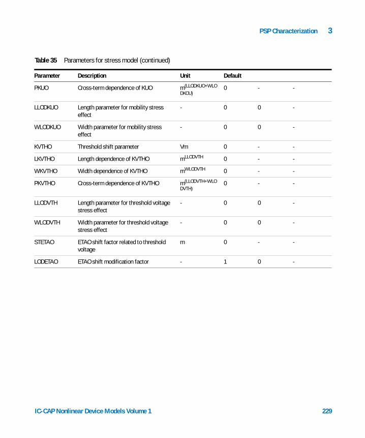
PSP Characterization 3
PKUO Cross-term dependence of KUO m(LLODKUO+WLO
DKOU)0 - -
LLODKUO Length parameter for mobility stress effect
- 0 0 -
WLODKUO Width parameter for mobility stress effect
- 0 0 -
KVTHO Threshold shift parameter Vm 0 - -
LKVTHO Length dependence of KVTHO mLLODVTH 0 - -
WKVTHO Width dependence of KVTHO mWLODVTH 0 - -
PKVTHO Cross-term dependence of KVTHO m(LLODVTH+WLO
DVTH)0 - -
LLODVTH Length parameter for threshold voltage stress effect
- 0 0 -
WLODVTH Width parameter for threshold voltage stress effect
- 0 0 -
STETAO ETAO shift factor related to threshold voltage
m 0 - -
LODETAO ETAO shift modification factor - 1 0 -
Table 35 Parameters for stress model (continued)
Parameter Description Unit Default
IC-CAP Nonlinear Device Models Volume 1 229

3 PSP Characterization
230 IC-CAP Nonlinear Device Models Volume 1

Agilent 85190A IC-CAP 2008Nonlinear Device Models Volume 1
4BSIM4 Characterization
Basic Effects Modeled in BSIM4 238
Key Features of the BSIM4 Modeling Package 239
DC Behavioral Modeling 240
CV Modeling 273
Structure of the BSIM4 RF Simulation Model 280
Test Structures for Deep Submicron CMOS Processes 297
SPICE Model Parameters for BSIM4.5.0 298
References 320
This chapter provides a theoretical background for the BSIM4 model. It is based on the model revision BSIM4.5.0, released by the University of California at Berkeley on July 29, 2005. Using the Modeling Packages is described in Chapter 1, “Using the MOS Modeling Packages.”
BSIM4.5.0 covers some improvements for geometric influences, temperature and processing variations. The details are described in “New features in the BSIM4 Modeling Package, Rev. IC-CAP 2006, April 2006.
BSIM4.4.0 addresses several new issues in modeling sub micron CMOS technology and RF high-speed CMOS circuit simulation. The BSIM4.3.0 model has been improved to cover such effects as trap assisted and gate overlap tunneling, recombination currents, and flicker noise.
The BSIM4.5.0 source code, BSIM4.5.0 user manual, BSIM4.5.0 new enhancement document and testing examples can be downloaded at [1]: http://www-device.eecs.berkeley.edu/~bsim3/bsim4_get.html
231Agilent Technologies
4 BSIM4 Characterization
What’s new inside the BSIM4 Modeling Package:
232
This section lists the enhancements and changes made to the Modeling Package for each revision since IC-CAP 2002. They are listed in reverse order so that the new version is on top, followed by former versions.
New features in the BSIM4 Modeling Package, Rev. IC-CAP 2006, April 2006
NOTE The supported model is now BSIM4.5.0, released by UCB in July 2005.
1.) General
The new effects modeled in BSIM4.5.0 are included as well as some improvements in handling the Modeling Package.
• A new mobility model, addressing Coulomb scattering as well as the mobility channel length dependence of heavily halo-doped devices
• Improved VOFF and VFBSDOFF temperature dependency
• Enhancements in temperature modeling using tempMod = 2: Vth(DITS) and gate tunneling models are functions of TNOM, temperature dependency of VFB is added
• A substrate resistance model (rbodyMod = 2), scalable with NF, L, and W
• XGW and NGCON can be specified as instance parameters
• Threshold voltage variation is represented by a new instance parameter, DELVTO
• Ion scattering effects during well implantation are modeled using an enhanced well-proximity effect model for parameters VTH, U0, K2
• Implementation of the VTH-model into the IGC-equation to allow modeling of the VBS dependence of IGC as well as IDS in the low current region
IC-CAP Nonlinear Device Models Volume 1

BSIM4 Characterization 4
IC-CAP Nonlinear Device Models Vo
2.) BSIM4_DC_CV_Extract
The extraction module gets some new features. Those handling improvements are described in Chapter 1, “Using the MOS Modeling Packages.”
• The data display now opens a multiplot window that displays an overview of plots using any number of plots in one window (up to 100), as well as zooming in on a specific plot instead of opening a new window for each plot.
• It is possible to arrange different types of plots and use them for extraction by means of the plot optimizer.
• You can display different devices, different temperatures, and different plot types with this multiplot window.
• The extraction flow is grouped into a global and a binning extraction part for a better overview. The groups can be expanded or deflated.
• Error calculation can be made visible in the plot window.
New features in the BSIM4 Modeling Package, Rev. IC-CAP 2006, November 2005
NOTE The supported model is now BSIM4.4.0, released by UCB in May 2004.
General
The new effects modeled in BSIM4.4.0 are included as well as some improvements in handling the Modeling Package. Those handling improvements are described in Chapter 1, “Using the MOS Modeling Packages.”
• Shallow Trench Isolation (STI) effects
• New temperature model
• Enhancements in the Holistic noise modeling
• Multilayer Gate tunneling current
• Tolerances in Binning
lume 1 233
234
4 BSIM4 Characterization
• Scalable Model has been enhanced for specific layouts using so called “Horseshoe contacts”
• Consistency check of DC measurement data included
• The time to load a new project has been dramatically reduced
• Extractions for BSIM4.3.0 specific parameters have been included
• New scheme to define de-embedding structures
New features in the BSIM4 Modeling Package, Rev. IC-CAP 2004, November 2004
NOTE The supported model is now BSIM4.3.0, released by UCB in May 2003.
General
The new effects modeled in BSIM4.3.0 are included as well as some improvements in handling the Modeling Package.
• Shallow Trench Isolation (STI) effects
• New temperature model
• Enhancements in the Holistic noise modeling
• Multilayer Gate tunneling current
• Tolerances in Binning
• Scalable Model has been enhanced for specific layouts using so called “Horseshoe contacts”
• Consistency check of DC measurement data included
• The time to loading a new project has been dramatically reduced
• Extractions for BSIM4.3.0 specific parameters have been included
• New scheme to define de-embedding structures
IC-CAP Nonlinear Device Models Volume 1

BSIM4 Characterization 4
IC-CAP Nonlinear Device Models Vo
New features in the BSIM4 Modeling Package, Rev. IC-CAP 2004, January 2004
1.) General
The BSIM4 Modeling Package can now generate model cards and scalable RF models for the following simulators:
Spice3 (delivered with IC-CAP)
Advanced Design System
Hspice
Spectre
All temperatures in setups and documentation are now given in [K] instead of [degree C]. Many suggestions from beta and first time users have been included into the Modeling Package.
2.) BSIM4_DC_CV_Measure
The Keithley switching matrix models K707 and K708a are supported.
The maximum compliance values can be defined together with the other measurement settings.
Three new functions are implemented to drive the BSIM4_DC_CV_Measure module from a wafer prober control macro. An example for such a control macro can be found in '.../examples /model_files/mosfet/bsim4/examples/waferprober/prober_control.mdl'
3.) BSIM4_DC_CV_Extract
A complete new extraction flow is implemented. A certain extraction group (e.g., 'Basic VTH, Mobility') can be invoked several times with different configurations.
4) BSIM4_RF_Extract
A complete new extraction flow is implemented. Please see the above noted BSIM4_DC_CV_Extract for more details.
lume 1 235

236
4 BSIM4 Characterization
The automatic generation of HTML files has been enhanced to include a navigation tree through all results.
New features in the BSIM4 Modeling Package, Rev. IC-CAP 2002, March 2003
The major enhancement in this update is the possibility to use the same set of measured data to extract parameters for the BSIM3 Model as well as for the BSIM4 Model.
This means, data generated by the BSIM3_DC_CV_Measure module can be imported into the BSIM4_DC_CV_Extract module and vice versa.
This feature allows the user to extract model parameters for use with the BSIM3 model as well as the BSIM4 model according to his needs, using only one set of measured data.
Moreover, the flow inside an extraction group can be specified in any desired order to get highest flexibility in adopting a specific parameter extraction to a certain process.
The automatic generation of binned model files is now supported. A new folder 'Binning' in the 'BSIM4_DC_CV_Extract' module allows the specification of binning areas as well as extended binning. Final circuits are generated for simulators supporting binned model parameters: Hspice, Spectre and ADS.
The automatic generation of HTML files has been enhanced to include a navigation tree through all results. In addition, all measured data at each temperature for each device is compared with the simulated results.
The new IC-CAP feature "Plot Optimizer" is supported through the use of an additional folder Plot Optimizer which allows the entering of devices and setups for a final fine tuning approach.
A new function is implemented to extract multiple projects in a batch mode. This can be very useful for statistical modeling, where a large number of model parameter sets have to be generated for the same type of devices but from different
IC-CAP Nonlinear Device Models Volume 1
BSIM4 Characterization 4
IC-CAP Nonlinear Device Models Vo
measured test chips. Please see the macro 'Example_Wafer_Extraction' in the BSIM4_DC_CV_Extract.mdl file.
Parameter extractions have been steadily enhanced due to user's feedback.
lume 1 237
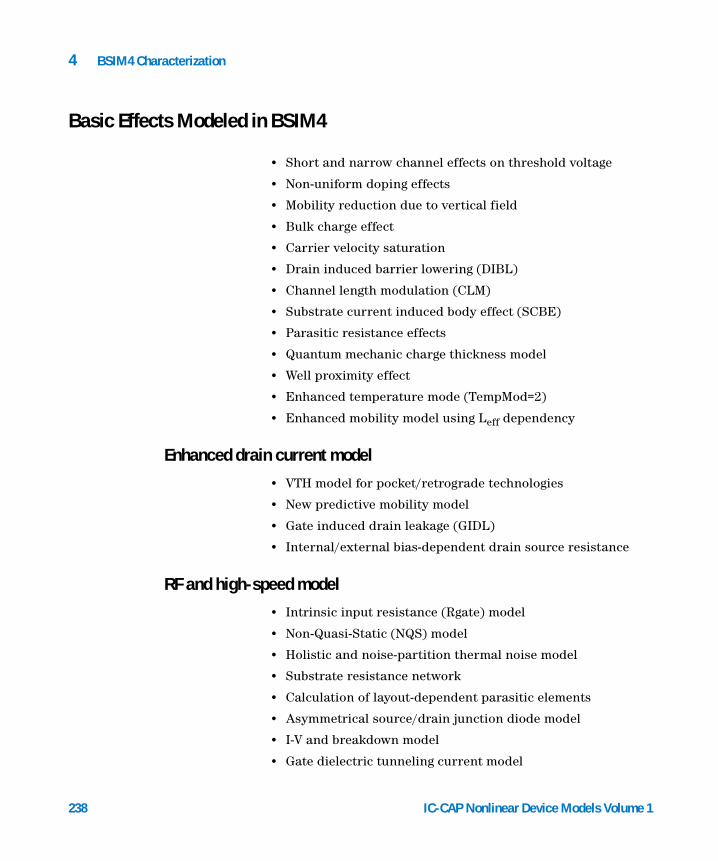
4 BSIM4 Characterization
Basic Effects Modeled in BSIM4
238
• Short and narrow channel effects on threshold voltage
• Non-uniform doping effects
• Mobility reduction due to vertical field
• Bulk charge effect
• Carrier velocity saturation
• Drain induced barrier lowering (DIBL)
• Channel length modulation (CLM)
• Substrate current induced body effect (SCBE)
• Parasitic resistance effects
• Quantum mechanic charge thickness model
• Well proximity effect
• Enhanced temperature mode (TempMod=2)
• Enhanced mobility model using Leff dependency
Enhanced drain current model
• VTH model for pocket/retrograde technologies
• New predictive mobility model
• Gate induced drain leakage (GIDL)
• Internal/external bias-dependent drain source resistance
RF and high-speed model
• Intrinsic input resistance (Rgate) model
• Non-Quasi-Static (NQS) model
• Holistic and noise-partition thermal noise model
• Substrate resistance network
• Calculation of layout-dependent parasitic elements
• Asymmetrical source/drain junction diode model
• I-V and breakdown model
• Gate dielectric tunneling current model
IC-CAP Nonlinear Device Models Volume 1
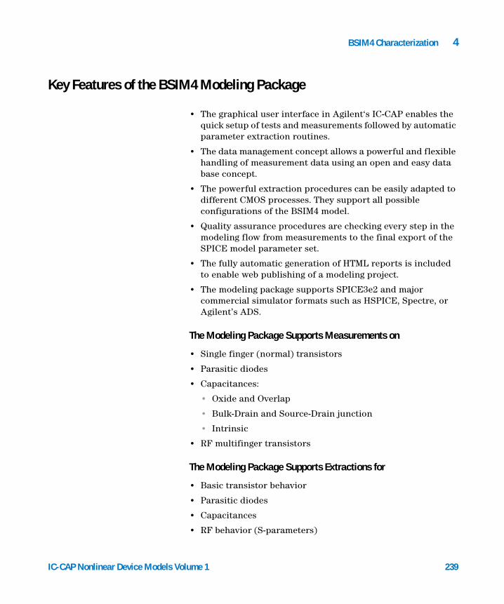
BSIM4 Characterization 4
Key Features of the BSIM4 Modeling Package
IC-CAP Nonlinear Device Models Vo
• The graphical user interface in Agilent‘s IC-CAP enables the quick setup of tests and measurements followed by automatic parameter extraction routines.
• The data management concept allows a powerful and flexible handling of measurement data using an open and easy data base concept.
• The powerful extraction procedures can be easily adapted to different CMOS processes. They support all possible configurations of the BSIM4 model.
• Quality assurance procedures are checking every step in the modeling flow from measurements to the final export of the SPICE model parameter set.
• The fully automatic generation of HTML reports is included to enable web publishing of a modeling project.
• The modeling package supports SPICE3e2 and major commercial simulator formats such as HSPICE, Spectre, or Agilent’s ADS.
The Modeling Package Supports Measurements on
• Single finger (normal) transistors
• Parasitic diodes
• Capacitances:
• Oxide and Overlap
• Bulk-Drain and Source-Drain junction
• Intrinsic
• RF multifinger transistors
The Modeling Package Supports Extractions for
• Basic transistor behavior
• Parasitic diodes
• Capacitances
• RF behavior (S-parameters)
lume 1 239
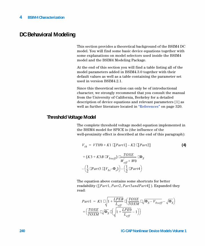
4 BSIM4 Characterization
DC Behavioral Modeling
240
This section provides a theoretical background of the BSIM4 DC model. You will find some basic device equations together with some explanations on model selectors used inside the BSIM4 model and the BSIM4 Modeling Package.
At the end of this section you will find a table listing all of the model parameters added in BSIM4.3.0 together with their default values as well as a table containing the parameter set used in version BSIM4.2.1.
Since this theoretical section can only be of introductional character, we strongly recommend that you consult the manual from the University of California, Berkeley for a detailed description of device equations and relevant parameters [1] as well as further literature located in “References” on page 320.
Threshold Voltage Model
The complete threshold voltage model equation implemented in the BSIM4 model for SPICE is (the influence of the well-proximity effect is described at the end of this paragraph):
(4)
The equation above contains some shortcuts for better readability ( ). Expanded they read:
Vth VTH0 K1 Part1[ ] K2 Part2[ ]
K( 3 K3B Vbseff )TOXE
Weff′
W0+------------------------- ΦS
12--- Part3⋅ Vbi Φs–( )⋅ –
12--- Part4⋅ –
⋅ ⋅ ⋅+ +
⋅–⋅+=
Part1 Part2 Part3andPart4,,[ ]
Part1 K1 1LPEB
Leff---------------+
TOXETOXM----------------- ΦS Vbseff– ΦS–⋅
TOXETOXM----------------- ΦS 1
LPE0Leff
--------------+ 1– ⋅ ⋅
+
⋅ ⋅=
IC-CAP Nonlinear Device Models Volume 1
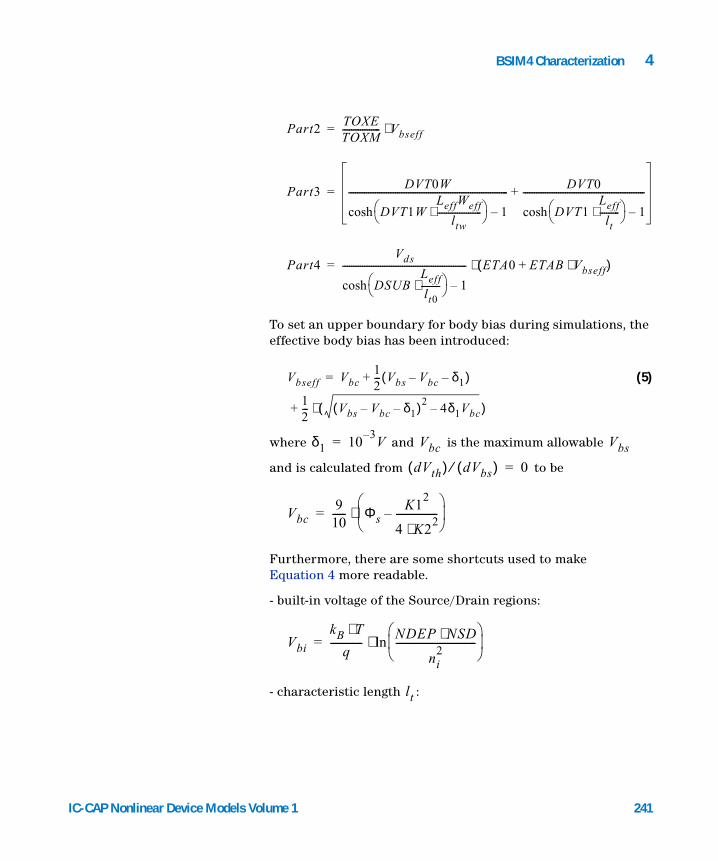
BSIM4 Characterization 4
IC-CAP Nonlinear Device Models Vo
To set an upper boundary for body bias during simulations, the effective body bias has been introduced:
(5)
where and is the maximum allowable
and is calculated from to be
Furthermore, there are some shortcuts used to make Equation 4 more readable.
- built-in voltage of the Source/Drain regions:
- characteristic length :
Part2TOXETOXM----------------- Vbseff⋅=
Part3DVT0W
DVT1WLeffWeff
ltw--------------------⋅
1–cosh
------------------------------------------------------------------------DVT0
DVT1Leff
lt---------⋅
1–cosh
-------------------------------------------------------+=
Part4Vds
DSUBLeff
lt0---------⋅
1–cosh
-------------------------------------------------------- ETA0 ETAB Vbseff⋅+( )⋅=
Vbseff Vbc12--- Vbs Vbc– δ1–( )
12--- Vbs Vbc– δ1–( )2
4δ1Vbc–( )⋅+
+=
δ1 103–V= Vbc Vbs
dVth( ) dVbs( )⁄ 0=
Vbc9
10------ Φs
K12
4 K22⋅
-----------------–
⋅=
Vbi
kB T⋅q
-------------NDEP NSD⋅
ni2
---------------------------------
ln⋅=
lt
lume 1 241
242
4 BSIM4 Characterization
and
- effective channel length and width, and :
lt
εsi TOXE2 εsi Φs Vbs–( )⋅ ⋅
q NDEP⋅--------------------------------------------⋅ ⋅
EPSROX-------------------------------------------------------------------------------- 1 DVT2 Vbs⋅+( )⋅=
lt0
εsi TOXE2 εsi Φs⋅ ⋅q NDEP⋅-------------------------⋅ ⋅
EPSROX-------------------------------------------------------------=
ltw
εsi TOXE2 εsi Φs⋅ ⋅q NDEP⋅-------------------------⋅ ⋅
EPSROX------------------------------------------------------------- 1 DVT2W Vbs⋅+( )⋅=
Leff Weff
Leff Ldrawn 2dL–=
Weff
Wdrawn
NF------------------ 2dW–=
Well-Proximity effect modeling
With BSIM4.5.0, the calculation of influences from the so called well-proximity has been introduced. Deep buried layers, possible by using high-energy implanters, affect devices located near the mask edge. Ions, scattered at the edge of the photo resist film, can influence the threshold voltage of those edge devices. A threshold voltage shift in the order of around 100 mV have been observed [1]. The following figure shows the effect [7].
IC-CAP Nonlinear Device Models Volume 1
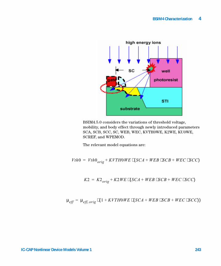
BSIM4 Characterization 4
IC-CAP Nonlinear Device Models Vo
BSIM4.5.0 considers the variations of threshold voltage, mobility, and body effect through newly introduced parameters SCA, SCB, SCC, SC, WEB, WEC, KVTH0WE, K2WE, KU0WE, SCREF, and WPEMOD.
The relevant model equations are:
Vth0 Vth0orig KVTH0WE SCA WEB SCB⋅ WEC SCC⋅+ +( )⋅+=
K2 K2orig K2WE SCA WEB SCB⋅ WEC SCC⋅+ +( )⋅+=
µeff µeff orig, 1 KVTH0WE+ SCA WEB SCB⋅ WEC SCC⋅+ +( )⋅( )⋅=
lume 1 243
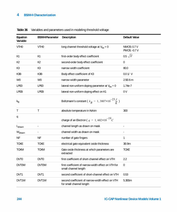
4 BSIM4 Characterization
Table 36 Variables and parameters used in modeling threshold voltage
Equation Variable
BSIM4 Parameter Description Default Value
VTH0 VTH0 long channel threshold voltage at Vbs = 0 NMOS: 0.7 VPMOS: -0.7 V
K1 K1 first-order body effect coefficient 0.5
K2 K2 second-order body effect coefficient 0
K3 K3 narrow width coefficient 80.0
K3B K3B Body effect coefficient of K3 0.0 1/ V
W0 W0 narrow width parameter 2.5E-6 m
LPE0 LPE0 lateral non-uniform doping parameter at Vbs = 0 1.74e-7
LPEB LPEB lateral non-uniform doping effect on K1 0 V
kB Boltzmann’s constant ( )
T T absolute temperature in Kelvin 300
qcharge of an Electron (
Ldrawn - channel length as drawn on mask -
Wdrawn - channel width as drawn on mask -
NF NF number of gate fingers 1
TOXE TOXE electrical gate equivalent oxide thickness 3E-9m
TOXM TOXM Gate oxide thickness at which parameters are extracted
TOXE
DVT0 DVT0 first coefficient of short-channel effect on VTH 2.2
DVT0W DVT0W first coefficient of narrow-width effect on VTH for small channel length
0
DVT1 DVT1 second coefficient of short-channel effect on VTH 0.53
DVT1W DVT1W second coefficient of narrow-width effect on VTH for small channel length
5.3E6m
V
kB 1 380723–×10, J
K----=
q 1 60219–×10, C=
244 IC-CAP Nonlinear Device Models Volume 1
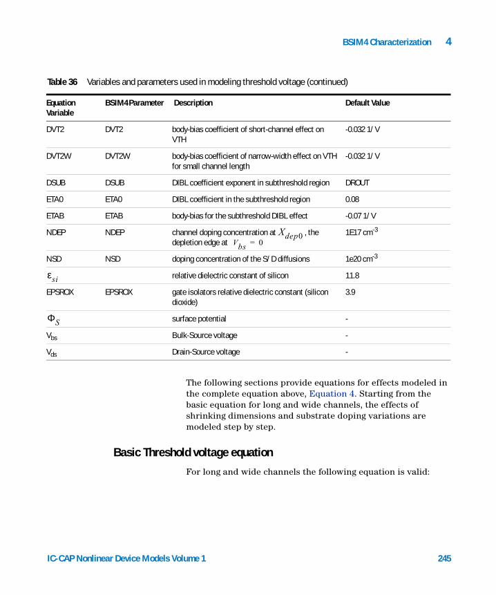
BSIM4 Characterization 4
DVT2 DVT2 body-bias coefficient of short-channel effect on VTH
-0.032 1/V
DVT2W DVT2W body-bias coefficient of narrow-width effect on VTH for small channel length
-0.032 1/V
DSUB DSUB DIBL coefficient exponent in subthreshold region DROUT
ETA0 ETA0 DIBL coefficient in the subthreshold region 0.08
ETAB ETAB body-bias for the subthreshold DIBL effect -0.07 1/V
NDEP NDEP channel doping concentration at , the depletion edge at
1E17 cm-3
NSD NSD doping concentration of the S/D diffusions 1e20 cm-3
relative dielectric constant of silicon 11.8
EPSROX EPSROX gate isolators relative dielectric constant (silicon dioxide)
3.9
surface potential -
Vbs Bulk-Source voltage -
Vds Drain-Source voltage -
Table 36 Variables and parameters used in modeling threshold voltage (continued)
Equation Variable
BSIM4 Parameter Description Default Value
Xdep0Vbs 0=
εsi
ΦS
IC-CAP Nonlinear Device Models Vo
The following sections provide equations for effects modeled in the complete equation above, Equation 4. Starting from the basic equation for long and wide channels, the effects of shrinking dimensions and substrate doping variations are modeled step by step.
Basic Threshold voltage equation
For long and wide channels the following equation is valid:
lume 1 245
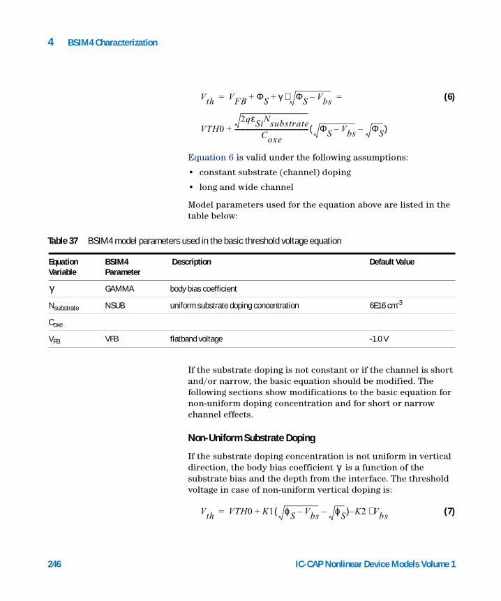
246
4 BSIM4 Characterization
(6)
Equation 6 is valid under the following assumptions:
• constant substrate (channel) doping
• long and wide channel
Model parameters used for the equation above are listed in the table below:
Vth VFB ΦS γ ΦS Vbs–⋅+ +
VTH02qεSiNsubstrate
Coxe------------------------------------------------ ΦS Vbs– ΦS–( )+
= =
used in the basic threshold voltage equation
Table 37 BSIM4 model parameters
Equation Variable
BSIM4 Parameter
Description Default Value
GAMMA body bias coefficient
Nsubstrate NSUB uniform substrate doping concentration 6E16 cm-3
Coxe
VFB VFB flatband voltage -1.0 V
γ
If the substrate doping is not constant or if the channel is short and/or narrow, the basic equation should be modified. The following sections show modifications to the basic equation for non-uniform doping concentration and for short or narrow channel effects.
Non-Uniform Substrate Doping
If the substrate doping concentration is not uniform in vertical direction, the body bias coefficient is a function of the substrate bias and the depth from the interface. The threshold voltage in case of non-uniform vertical doping is:
(7)
γ
Vth VTH0 K1 ϕS Vbs– ϕS–( )+ K– 2 Vbs⋅=
IC-CAP Nonlinear Device Models Volume 1

BSIM4 Characterization 4
IC-CAP Nonlinear Device Models Vo
where
The doping profile is assumed to be a steep retrograde and is approximated in BSIM4. For details on how it is modeled, see the manual from UC Berkeley [1] starting on page 2-2. The model parameters K1 and K2 can be calculated from NSUB, XT, VBX, VBM, and so on. This is done the same way as in BSIM3v3. Details can be found on page 2-4 of the BSIM4 manual.
ϕS4
10------
kBT
q----------⋅ NDEP
ni---------------- PHIN+ln⋅=
ping model parameters
Table 38 Non-uniform substrate doEquation Variable
BSIM4 Parameter
Description Default Value
ni intrinsic carrier concentration in the channel region
PHIN PHIN Non-uniform vertical doping effect on surface potential
0.0
Non-Uniform Lateral Doping: Pocket or Halo Implant
The doping concentration in this case varies from the middle of the channel towards the source/drain junctions. Shorter channel lengths will result in a roll-up of from the rise of the effective channel doping concentration and the changes of the body bias effect. Those effects are considered using the following formulation:
(8)
Additionally, drain-induced threshold shift (DITS) has to be considered in long-channel devices using pocket implant. For
in a range of interest, a simplified threshold voltage shift caused by DITS was implemented:
Vth
Vth VTH0 K1 Φs Vbs– Φs– )( 1LPEBLeff
---------------+
K2 Vbs⋅– K1 1LPE0Leff
--------------+ 1–
Φs⋅ ⋅+
⋅ ⋅+=
Vds
lume 1 247

248
4 BSIM4 Characterization
(9)
Using TEMPMOD=2, this formula changes to
(10)
Short-Channel and Drain-Induced-Barrier-Lowering (DIBL) Effects
For shorter channels, the threshold voltage is more sensitive to drain bias (DIBL effect) and less sensitive to body bias because of reduced control of the depletion region.
The short channel effect coefficient is given by
In BSIM3v3 this equation is approximated, which results in a phantom second roll-up when Leff becomes very small. To avoid this effect, the exact formulation is used in BSIM4. Model flexibility is increased for different technologies with additional parameters introduced and the short-channel and drain-induced-barrier-lowering effects are modeled separately.
This leads to a short-channel effect coefficient of the form:
Vth∆ DITS( ) nνt–Leff
Leff DVTP0 1 eDVTP1 Vds⋅–
+ ⋅+
-----------------------------------------------------------------------------------------------
ln⋅=
Vth∆ DITS( ) nνtnom–Leff
Leff DVTP0 1 eDVTP1 Vds⋅–
+
⋅+
-----------------------------------------------------------------------------------------------
ln⋅=
θth Leff( ) 1
2Leff
lt----------
1–cosh
---------------------------------------------=
IC-CAP Nonlinear Device Models Volume 1
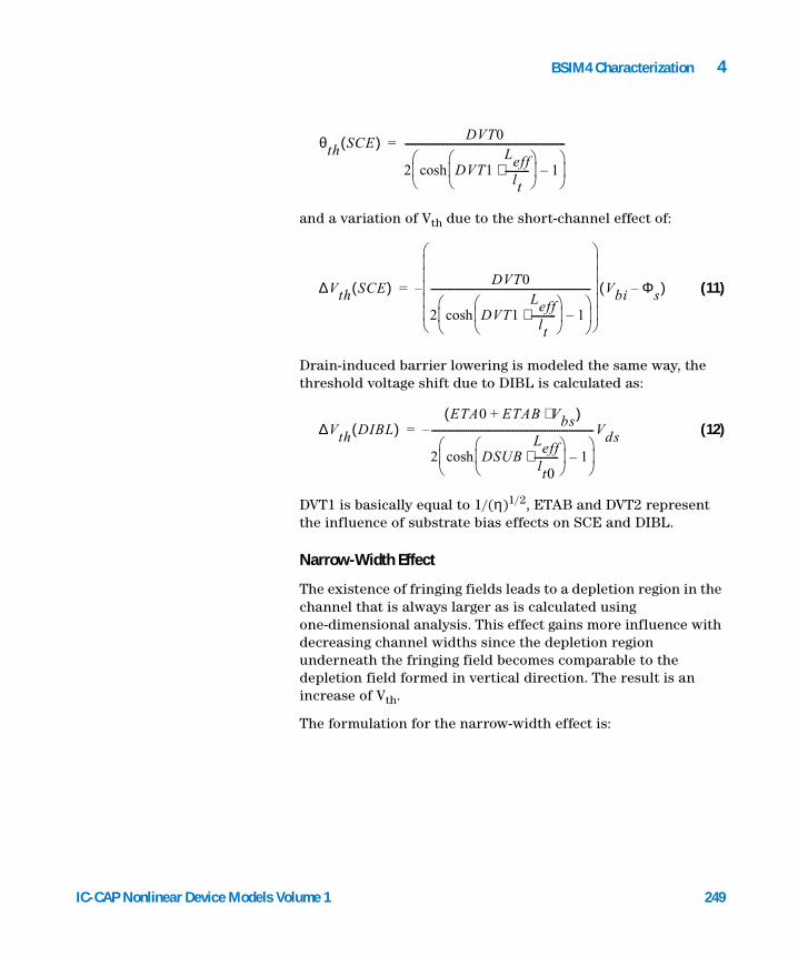
BSIM4 Characterization 4
IC-CAP Nonlinear Device Models Vo
and a variation of Vth due to the short-channel effect of:
(11)
Drain-induced barrier lowering is modeled the same way, the threshold voltage shift due to DIBL is calculated as:
(12)
DVT1 is basically equal to 1/(η)1/2, ETAB and DVT2 represent the influence of substrate bias effects on SCE and DIBL.
Narrow-Width Effect
The existence of fringing fields leads to a depletion region in the channel that is always larger as is calculated using one-dimensional analysis. This effect gains more influence with decreasing channel widths since the depletion region underneath the fringing field becomes comparable to the depletion field formed in vertical direction. The result is an increase of Vth.
The formulation for the narrow-width effect is:
θth SCE( ) DVT0
2 DVT1Leff
lt----------⋅
1–cosh
-----------------------------------------------------------------=
∆Vth SCE( ) DVT0
2 DVT1Leff
lt----------⋅
1–cosh
-----------------------------------------------------------------
Vbi Φs–( )–=
∆Vth DIBL( )ETA0 ETAB V⋅+ bs( )
2 DSUBLefflt0
----------⋅
1–cosh
------------------------------------------------------------------Vds–=
lume 1 249
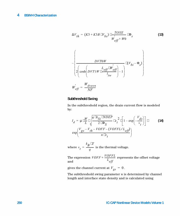
250
4 BSIM4 Characterization
(13)
Subthreshold Swing
In the subthreshold region, the drain current flow is modeled by:
(14)
where is the thermal voltage.
The expression represents the offset voltage and
gives the channel current at .
The subthreshold swing parameter n is determined by channel length and interface state density and is calculated using
∆Vth K3 K3B Vbs⋅+( ) TOXE
Weff′
W0+-------------------------- Φs
DVT0W
2 DVT1WLeff Weff
′⋅
ltw--------------------------⋅
cosh 1–
--------------------------------------------------------------------------------------- Vbi Φs–( )⋅
–
⋅ ⋅=
Weff′ Wdrawn
NF------------------=
Id µ WL-----
q εSi NDEP⋅ ⋅
2 ΦS⋅------------------------------------ vt
21
Vdsvt
---------–
exp–
Vgs Vth– VOFF– VOFFL Leff⁄( )–
n vt⋅--------------------------------------------------------------------------------------------
exp
⋅ ⋅ ⋅ ⋅ ⋅=
vt
kB T⋅
q--------------=
VOFFVOFFL
Leff--------------------+
Vgs 0=
IC-CAP Nonlinear Device Models Volume 1
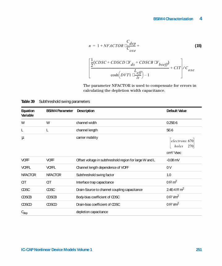
BSIM4 Characterization 4
IC-CAP Nonlinear Device Models Vo
(15)
The parameter NFACTOR is used to compensate for errors in calculating the depletion width capacitance.
n 1 NFACTORCdepCoxe-------------⋅
12--- CDSC CDSCD Vds⋅ CDSCB Vbseff⋅+ +( )
DVT1Leff
lt----------⋅
cosh 1–
------------------------------------------------------------------------------------------------------------------ CIT+ Coxe⁄
+ +=
Table 39 Subthreshold swing parameters
Equation Variable
BSIM4 Parameter Description Default Value
W W channel width 0.25E-6
L L channel length 5E-6
carrier mobility
cm²/Vsec
VOFF VOFF Offset voltage in subthreshold region for large W and L -0.08 mV
VOFFL VOFFL Channel length dependence of VOFF 0 V
NFACTOR NFACTOR Subthreshold swing factor 1.0
CIT CIT Interface trap capacitance 0 F/m2
CDSC CDSC Drain-Source to channel coupling capacitance 2.4E-4 F/m2
CDSCB CDSCB Body-bias coefficient of CDSC 0 F/Vm2
CDSCD CDSCD Drain-bias coefficient of CDSC 0 F/Vm2
Cdep depletion capacitance
µelectrons 670
holes 270
lume 1 251
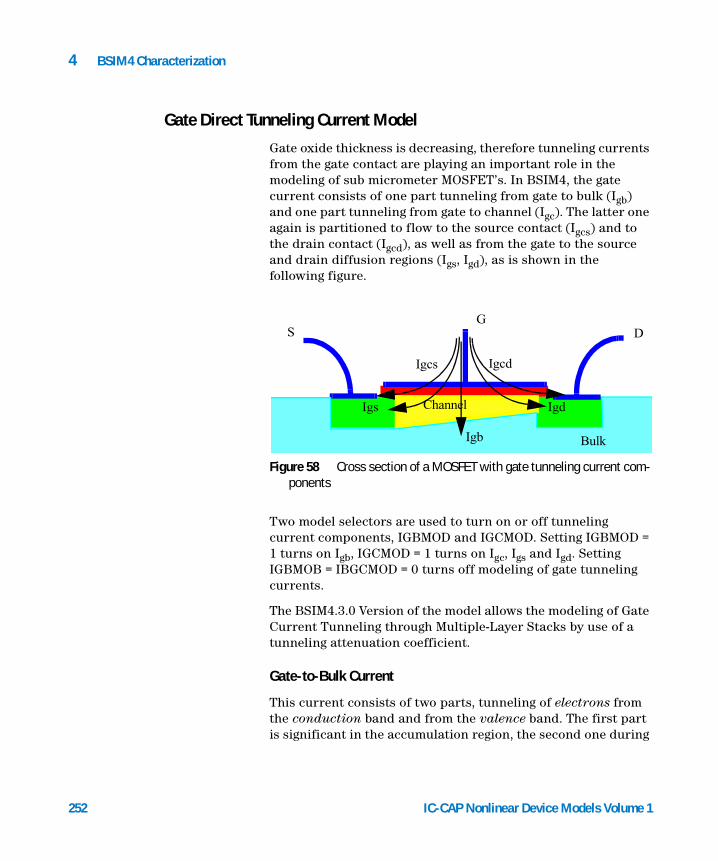
4 BSIM4 Characterization
Gate Direct Tunneling Current Model
252
Gate oxide thickness is decreasing, therefore tunneling currents from the gate contact are playing an important role in the modeling of sub micrometer MOSFET’s. In BSIM4, the gate current consists of one part tunneling from gate to bulk (Igb) and one part tunneling from gate to channel (Igc). The latter one again is partitioned to flow to the source contact (Igcs) and to the drain contact (Igcd), as well as from the gate to the source and drain diffusion regions (Igs, Igd), as is shown in the following figure.
Two model selectors are used to turn on or off tunneling current components, IGBMOD and IGCMOD. Setting IGBMOD = 1 turns on Igb, IGCMOD = 1 turns on Igc, Igs and Igd. Setting IGBMOB = IBGCMOD = 0 turns off modeling of gate tunneling currents.
The BSIM4.3.0 Version of the model allows the modeling of Gate Current Tunneling through Multiple-Layer Stacks by use of a tunneling attenuation coefficient.
Gate-to-Bulk Current
This current consists of two parts, tunneling of electrons from the conduction band and from the valence band. The first part is significant in the accumulation region, the second one during
Figure 58 Cross section of a MOSFET with gate tunneling current com-ponents
GDS
Bulk
Channel
Igcd
Igd
Igcs
Igs
Igb
IC-CAP Nonlinear Device Models Volume 1

BSIM4 Characterization 4
IC-CAP Nonlinear Device Models Vo
device inversion. The accumulation region tunneling current is dominated by electron tunneling from the conduction band and is given by:
(16)
Inside this equation, the auxiliary voltage is:
(17)
The constants in this equation are:
A = 4.97232E-7 A/V²
B = 7.45669E11 (g/F-s²)0.5
The tunneling current dominating the inversion region is caused by electron tunneling from the valence band. It is calculated by:
(18)
Inside this equation, the auxiliary voltage is:
Igbacc Weff Leff ATOXREF
TOXE------------------------
NTOX 1
TOXE2
------------------- Vgb
Vaux1 B TOXE AIGBACC BIGBACC Voxacc⋅–( )
1 CIGBACC Voxacc⋅+( ) ]
⋅⋅–[exp
⋅ ⋅ ⋅ ⋅ ⋅
⋅ ⋅
=
Vaux1 NIGBACC vt( )
1Vgb Vfbzb–
NIGBACC vt⋅------------------------------------–
exp+
log
⋅
⋅
=
Igbinv Weff Leff CTOXREF
TOXE------------------------
NTOX 1
TOXE2
------------------- Vgb
Vaux2 D TOXE AIGBINV BIGBINV Voxdepinv⋅–( )
1 CIGB ACCINV( ) Voxdepinv⋅+( ) ]⋅
⋅–[exp
⋅ ⋅ ⋅ ⋅ ⋅
⋅ ⋅
=
lume 1 253
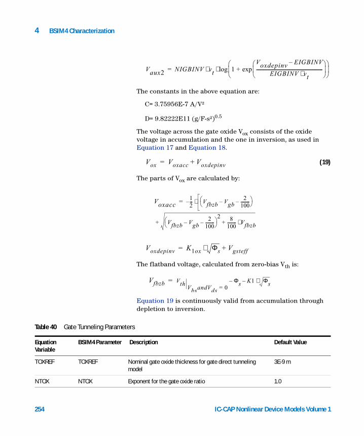
254
4 BSIM4 Characterization
The constants in the above equation are:
C= 3.75956E-7 A/V²
D= 9.82222E11 (g/F-s²)0.5
The voltage across the gate oxide Vox consists of the oxide voltage in accumulation and the one in inversion, as used in Equation 17 and Equation 18.
(19)
The parts of Vox are calculated by:
The flatband voltage, calculated from zero-bias Vth is:
Equation 19 is continuously valid from accumulation through depletion to inversion.
Vaux2 NIGBINV vt 1Voxdepinv EIGBINV–
EIGBINV vt⋅-----------------------------------------------------------
exp+
log⋅ ⋅=
Vox Voxacc Voxdepinv+=
Voxacc12---– Vfbzb Vgb–
2100---------–
Vfbzb Vgb–2
100---------–
2 8
100--------- Vfbzb⋅++
⋅=
Voxdepinv K1ox Φs Vgsteff+⋅=
Vfbzb VthVbsandVds 0=
Φs– K1 Φs⋅–=
Table 40 Gate Tunneling Parameters
Equation Variable
BSIM4 Parameter Description Default Value
TOXREF TOXREF Nominal gate oxide thickness for gate direct tunneling model
3E-9 m
NTOX NTOX Exponent for the gate oxide ratio 1.0
IC-CAP Nonlinear Device Models Volume 1
BSIM4 Characterization 4
AIGBACC AIGBACC Parameter for Igb in accumulation 0.43
BIGBACC BIGBACC Parameter for Igb in accumulation 0.054
CIGBACC CIGBACC Parameter for Igb in accumulation 0.075
NIGBACC NIGBACC Parameter for Igb in accumulation 1.0
AIGBINV AIGBINV Parameter for Igb in inversion 0.35
BIGBINV BIGBINV Parameter for Igb in inversion 0.03
CIGBINV CIGBINV Parameter for Igb in inversion 0.006
NIGBINV NIGBINV Parameter for Igb in inversion 1.1
Table 40 Gate Tunneling Parameters (continued)
Equation Variable
BSIM4 Parameter Description Default Value
IC-CAP Nonlinear Device Models Vo
Gate-to-Channel Current Igc
The gate-to-channel current is determined by electrons tunneling from the conduction band in NMOS transistors respective holes tunneling from the valence band in PMOS transistors.
(20)
The physical constants E and F are listed in Table 41.
Igc Weff Leff ETOXREF
TOXE------------------------ NTOX 1
TOXE2
------------------ Vgse
NIGC vt 1Vgse VTH0–
NIGC vt⋅--------------------------------
exp+
log
F TOXE AIGC BIGC Voxdepinv⋅–( )
1 CIGC Voxdepinv⋅+( )
⋅ ⋅
⋅
–[
]
exp
⋅ ⋅
⋅ ⋅ ⋅
⋅
⋅ ⋅ ⋅=
lume 1 255

256
4 BSIM4 Characterization
Gate-to-Source and Gate-to-Drain tunneling currents
These currents tunnel from the gate contact to the source or drain diffusion regions. They are caused by electron tunneling from the conduction band in NMOS transistors and by hole tunneling from the valence band in PMOS transistors.
(21)
For the computing of Igd, the values of Vgs in Equation 21 has to be replaced by Vgd.
The flat-band voltage between and the source or drain diffusion areas is dependent from NGATE:
If NGATE >0.0:
Else:
To take drain bias effects into account, the tunneling current from the gate contact splits into two components and it is
. The components are calculated as:
Igs Weff DLCIG E ToxRatioEdge Vgs
Vgs′
F– TOXE POXEDGE
AIGSD BIGSD Vgs′⋅( )–( ) 1 CIGSD Vgs
′⋅+( )
⋅ ⋅
⋅ ⋅
[
]
exp
⋅ ⋅ ⋅ ⋅
⋅ ⋅
=
Vgs′
Vgs Vfbsd–( )21e 4–( )+=
Vfbsd
kBT
q---------
NGATENSD
-------------------- log⋅=
Vfbsd 0=
Igc Igcs Igcd+=
Igcs Igc
PIGCD Vds PIGCD– Vds⋅( )exp 1– 1e 4–( )+ +⋅
PIGCD2
Vds2
2e 4–( )+⋅-----------------------------------------------------------------------------------------------------------------------------⋅=
Igcd Igc
1 PIGCD V⋅ ds 1+( )– PIGCD– Vds⋅( )exp 1e 4–( )+
PIGCD2
Vds2
2e 4–( )+⋅----------------------------------------------------------------------------------------------------------------------------------⋅=
IC-CAP Nonlinear Device Models Volume 1
BSIM4 Characterization 4
IC-CAP Nonlinear Device Models Vo
If the model parameter PIGCD is not specified, it is calculated by:
(22)
The constants used in Equation 21 and Equation 22 have different values for NMOS and PMOS transistors:
Table 41 Values of constants for gate-channel and gate S/D tunneling
NMOS PMOS
E 4.97232 A/V² 3.42537 A/V²
F 7.45669E11 1.16645E12
PIGCDB TOXE⋅
Vgsteff2
------------------------ 1Vdseff
2 Vgsteff⋅-----------------------–
⋅=
g F s2
–( )⁄ g F s2
–( )⁄
Table 42 Gate Tunneling Parameters (continued from Table 40)
Equation Variable
BSIM4 Parameter
Description Default Value
DLCIG DLCIG Source/Drain overlap length for Igs and Igd LINT
POXEDGE POXEDGE Factor for gate oxide thickness in source/drain overlap regions
1.0
AIGSD AIGSD Parameter for Igs and Igd NMOS: 0.43PMOS: 0.31
BIGSD BIGSD Parameter for Igs and Igd NMOS: 0.054PMOS: 0.024
Fs2( ) g⁄
m-------------------------
Fs2( ) g⁄
m V⋅-------------------------
lume 1 257
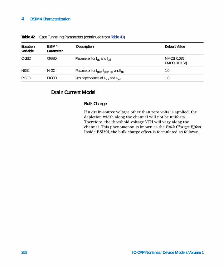
4 BSIM4 Characterization
Drain Current Model
CIGSD CIGSD Parameter for Igs and Igd NMOS: 0.075PMOS: 0.03 [V]
NIGC NIGC Parameter for Igcs, Igcd, Igs and Igd 1.0
PIGCD PIGCD Vgs dependence of Igcs and Igcd 1.0
Table 42 Gate Tunneling Parameters (continued from Table 40)
Equation Variable
BSIM4 Parameter
Description Default Value
258
Bulk Charge
If a drain-source voltage other than zero volts is applied, the depletion width along the channel will not be uniform. Therefore, the threshold voltage VTH will vary along the channel. This phenomenon is known as the Bulk Charge Effect. Inside BSIM4, the bulk charge effect is formulated as follows:
IC-CAP Nonlinear Device Models Volume 1
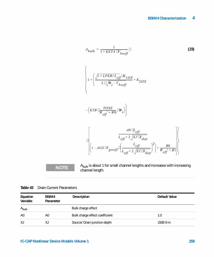
BSIM4 Characterization 4
IC-CAP Nonlinear Device Models Vo
(23)Abulk1
1 KETA Vbseff⋅+----------------------------------------------
11 LPEB Leff⁄+ K1OX⋅
2 Φs Vbseff–⋅--------------------------------------------------------------- K2OX
K3BTOXE
Weff ′ W0+---------------------------- Φs⋅ ⋅
–
+
A0 Leff⋅
Leff 2 XJ Xdep⋅+------------------------------------------------
1 AGS Vgsteff
Leff
Leff 2 XJ Xdep⋅+------------------------------------------------ 2
⋅ ⋅– B0
Weff′ B1+---------------------------+
⋅
+
⋅=
NOTE Abulk is about 1 for small channel lengths and increases with increasing channel length.
Table 43 Drain Current Parameters
Equation Variable
BSIM4 Parameter
Description Default Value
Abulk Bulk charge effect
A0 A0 Bulk charge effect coefficient 1.0
XJ XJ Source/Drain junction depth 150E-9 m
lume 1 259
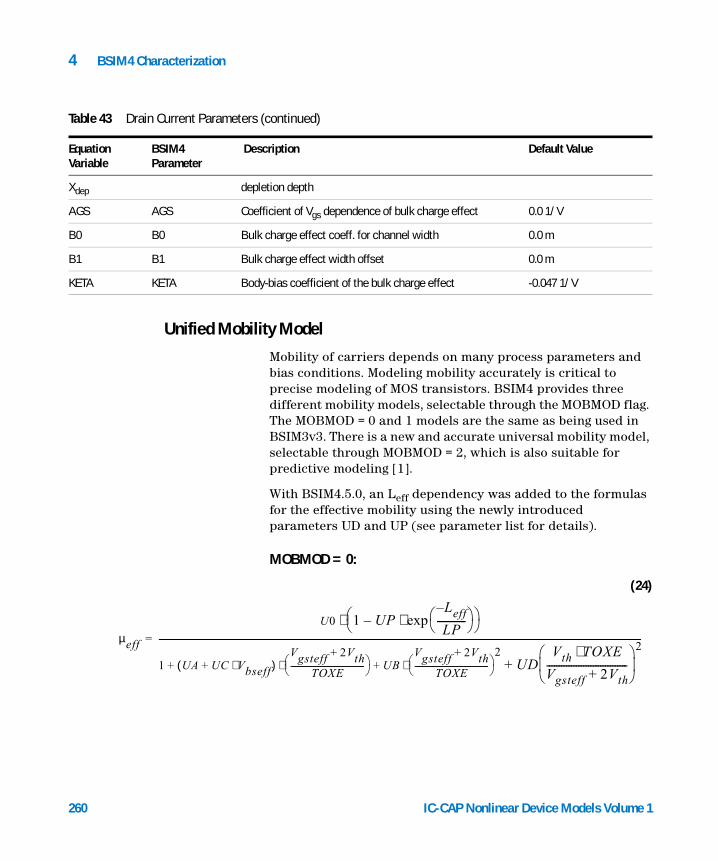
4 BSIM4 Characterization
Unified Mobility Model
Xdep depletion depth
AGS AGS Coefficient of Vgs dependence of bulk charge effect 0.0 1/V
B0 B0 Bulk charge effect coeff. for channel width 0.0 m
B1 B1 Bulk charge effect width offset 0.0 m
KETA KETA Body-bias coefficient of the bulk charge effect -0.047 1/V
Table 43 Drain Current Parameters (continued)
Equation Variable
BSIM4 Parameter
Description Default Value
260
Mobility of carriers depends on many process parameters and bias conditions. Modeling mobility accurately is critical to precise modeling of MOS transistors. BSIM4 provides three different mobility models, selectable through the MOBMOD flag. The MOBMOD = 0 and 1 models are the same as being used in BSIM3v3. There is a new and accurate universal mobility model, selectable through MOBMOD = 2, which is also suitable for predictive modeling [1].
With BSIM4.5.0, an Leff dependency was added to the formulas for the effective mobility using the newly introduced parameters UD and UP (see parameter list for details).
MOBMOD = 0:
(24)
µeff
U0 1 UPLeff–
LP------------ exp⋅–
⋅
1 UA UC V⋅ bseff+( )Vgsteff 2Vth+
TOXE------------------------------------- ⋅ UB
Vgsteff 2Vth+
TOXE-------------------------------------
2UD
Vth TOXE⋅Vgsteff 2Vth+--------------------------------- 2
+⋅+ +
--------------------------------------------------------------------------------------------------------------------------------------------------------------------------------------------------------------------------------------------------=
IC-CAP Nonlinear Device Models Volume 1
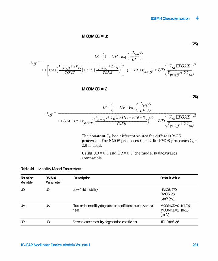
BSIM4 Characterization 4
IC-CAP Nonlinear Device Models Vo
MOBMOD = 1:
(25)
µeff
U0 1 UPLeff–
LP------------ exp⋅–
⋅
1 UAVgsteff 2Vth+
TOXE------------------------------------- ⋅ UB
Vgsteff 2Vth+
TOXE-------------------------------------
2⋅+ 1 UC Vbseff⋅+( ) UD
Vth TOXE⋅Vgsteff 2Vth+--------------------------------- 2
+⋅+
---------------------------------------------------------------------------------------------------------------------------------------------------------------------------------------------------------------------------------------------------------------=
MOBMOD = 2
(26)
µeff
U0 1 UPLeff–
LP------------ exp⋅–
⋅
1 UA UC Vbseff⋅+( )Vgsteff C0 VTH0 VFB– Φs–(⋅+
TOXE-------------------------------------------------------------------------------------
EUUD
Vth TOXE⋅Vgsteff 2Vth+--------------------------------- 2
+ +
------------------------------------------------------------------------------------------------------------------------------------------------------------------------------------------------------------------------------------=
The constant C0 has different values for different MOS processes. For NMOS processes C0 = 2, for PMOS processes C0 = 2.5 is used.
Using UD = 0.0 and UP = 0.0, the model is backwards compatible.
Table 44 Mobility Model Parameters
Equation Variable
BSIM4 Parameter
Description Default Value
U0 U0 Low-field mobility NMOS: 670 PMOS: 250[cm²/(Vs)]
UA UA First-order mobility degradation coefficient due to vertical field
MOBMOD=0, 1: 1E-9MOBMOD=2: 1e-15[m/V]
UB UB Second-order mobility degradation coefficient 1E-19 (m/V)²
lume 1 261
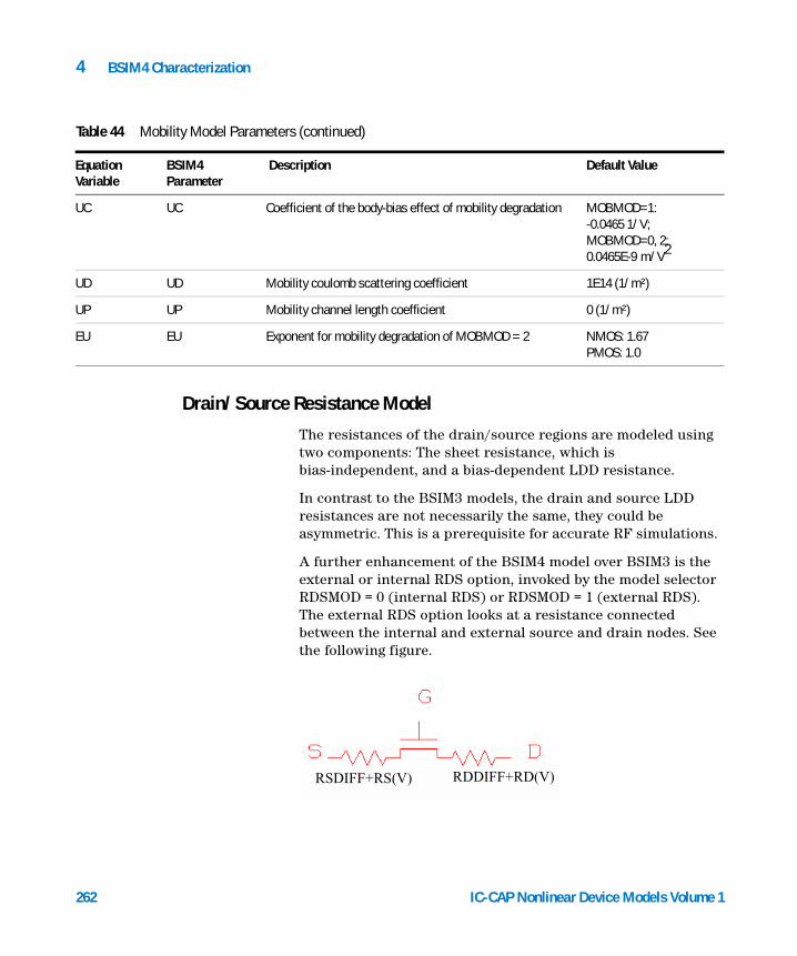
4 BSIM4 Characterization
Drain/Source Resistance Model
UC UC Coefficient of the body-bias effect of mobility degradation MOBMOD=1: -0.0465 1/V;MOBMOD=0, 2: 0.0465E-9 m/V2
UD UD Mobility coulomb scattering coefficient 1E14 (1/m²)
UP UP Mobility channel length coefficient 0 (1/m²)
EU EU Exponent for mobility degradation of MOBMOD = 2 NMOS: 1.67PMOS: 1.0
Table 44 Mobility Model Parameters (continued)
Equation Variable
BSIM4 Parameter
Description Default Value
262
The resistances of the drain/source regions are modeled using two components: The sheet resistance, which is bias-independent, and a bias-dependent LDD resistance.
In contrast to the BSIM3 models, the drain and source LDD resistances are not necessarily the same, they could be asymmetric. This is a prerequisite for accurate RF simulations.
A further enhancement of the BSIM4 model over BSIM3 is the external or internal RDS option, invoked by the model selector RDSMOD = 0 (internal RDS) or RDSMOD = 1 (external RDS). The external RDS option looks at a resistance connected between the internal and external source and drain nodes. See the following figure.
RSDIFF+RS(V) RDDIFF+RD(V)
IC-CAP Nonlinear Device Models Volume 1

BSIM4 Characterization 4
IC-CAP Nonlinear Device Models Vo
RDSMOD = 0 (internal Rs(V))
(27)
RDSMOD = 1 (external Rd(V) and Rs(V))
(28)
(29)
The flatband voltage Vfbsd is calculated as follows:
If NGATE > 0:
Else:
Rds V( ) 1
1e6 Weffcj⋅( )WR--------------------------------------------
RDSWMIN RDSW+
PRWB Φs Vbseff– Φs–( )⋅ 11 PRWG Vgsteff⋅+--------------------------------------------------+
=
Rd V( ) 1
1e6 Weffcj⋅( )WRNF⋅
---------------------------------------------------------
RDSWMIN RDSW+
PRWB Vbd⋅–1
1 PRWG Vgd Vfbsd–( )⋅+-------------------------------------------------------------------+
=
Rs V( ) 1
1e6 Weffcj⋅( )WRNF⋅
---------------------------------------------------------
RDSWMIN RDSW+
PRWB Vbs⋅–1
1 PRWG Vgs Vfbsd–( )⋅+-------------------------------------------------------------------+
=
Vfbsd
kB T⋅
q--------------
NGATENSD
-------------------- log⋅=
Vfbsd 0=
lume 1 263
4 BSIM4 Characterization
Saturation Region Output Conductance Model
Table 45 Drain Source Resistance Parameters
Equation Variable
BSIM4 Parameter
Description Default Value
NGATE NGATE Poly Si-gate doping concentration 0.0 cm-3
PRWB PRWB Body bias coefficient of LDD resistance 0.0 V-0.5
PRWG PRWG Gate bias dependence of LDD resistance 1.0 1/V
RDSW RDSW Zero bias LDD resistance per unit width for RDSMOD = 0 200 (µm)WR
RDSWMIN RDSWMIN LDD resistance per unit width at high Vgs and zero Vbs for RDSMOD = 0
0.0 (µm)WR
WR WR Channel width dependence parameter of LDD resistance 1.0
Ω
Ω
264
The following figure shows a typical MOSFET Ids vs. Vds diagram. The calculated output resistance is inserted into the diagram as well. This output resistance curve can be divided into four distinct regions, each region is affected by different physical effects. The first region at low Vds is characterized by a very small output resistance. It is called the linear region, where carrier velocity is not yet saturated.
Increasing Vds leads to a region that is dominated by carrier velocity saturation; this is the so-called saturation region. In this region, three different physical mechanisms are controlling device behavior. Those mechanisms are Channel Length Modulation (CLM), Drain-Induced Barrier Lowering (DIBL), and Substrate-Current Induced Body Effect (SCBE). Each of those mechanisms dominate the output resistance in a specific region.
IC-CAP Nonlinear Device Models Volume 1

BSIM4 Characterization 4
IC-CAP Nonlinear Device Models Vo
The continuous channel current equation for the linear and saturation region as implemented in BSIM4 is:
(30)
Figure 59 Output Resistance vs. Drain-Source Voltage [1]
Ids
Ids0 NF⋅
1Rds Ids0⋅
Vdseff-------------------------+
-----------------------------------
11
Cclm-------------
VAsat VACLM+
VAsat-------------------------------------------
ln⋅+
1Vds Vdseff–
VADIBL--------------------------------+
1Vds Vdseff–
VADITS--------------------------------+
⋅
1
Vds Vdseff–
VASCBE--------------------------------+
⋅
=
lume 1 265

266
4 BSIM4 Characterization
The Early voltage VAsat at is used to get continuous expressions for drain current and output resistance between linear and saturation region.
(31)
In this equation, the channel current dependencies are modeled using specific Early voltages VA, as will be described in the following sections.
Channel Length Modulation - CLM
Through integration based on a quasi two-dimensional analysis, we obtain
(32)
Vds Vdsat=
VAsat 1Abulk Vdsat⋅
2 Vgsteff 2kB T⋅
q--------------+
⋅
--------------------------------------------------------–
Esat Leff⋅ Vdsat 2 Rds vsat Coxe Weff Vgsteff⋅ ⋅ ⋅ ⋅ ⋅+ +
Rds vsat Coxe Weff Abulk⋅ ⋅ ⋅ ⋅ 1–2λ---+
-----------------------------------------------------------------------------------------------------------------------------------------------⋅
=
VACLM1
PCLM-----------------
Vds Vdsat–( )
1 FPROUTLeff
Vgsteff 2kB T⋅
q--------------⋅+
-----------------------------------------------⋅+
--------------------------------------------------------------------------------------
1 PVAGVgsteff
Esat Leff⋅--------------------------⋅+
1Rds Idso⋅
Vdseff-------------------------+
Leff
VdsatEsat
--------------+ εsi TOXE XJ⋅ ⋅
EPSROX---------------------------------------
⋅
⋅
⋅ ⋅ ⋅
=
IC-CAP Nonlinear Device Models Volume 1

BSIM4 Characterization 4
IC-CAP Nonlinear Device Models Vo
Drain-Induced Barrier Lowering - DIBL
The gate voltage modulates the DIBL effect. To correctly model DIBL, the parameter PDIBLC2 is introduced. This parameter becomes significant only for long channel devices.
(33)
The parameter is channel length dependent in the same manner as the DIBL effect in VTH, but different parameters are used here.
Substrate-Current Induced Body Effect - SCBE
Due to increasing Vds, some electrons flowing from the source of an NMOS device will gain high energies and are able to cause impact ionization. Electron-hole pairs will be generated and the substrate current created by impact ionization will increase exponentially with the drain voltage. The early voltage due to SCBE is calculated by
(34)
VADIBL
Vgsteff 2νt+
θrout 1 PDIBLCB Vbsteff⋅+( )⋅-----------------------------------------------------------------------------------
1Abulk Vdsat⋅
Abulk Vdsat⋅ Vgsteff 2kB T⋅
q--------------+ +
------------------------------------------------------------------------------------–
1 PVAGVgsteff
Esat Leff⋅--------------------------⋅+
⋅
⋅
=
θrout
θroutPDIBLC1
2DROUT Leff⋅
lt0------------------------------------ cosh⋅ 2–
---------------------------------------------------------------------- PDIBLC2+=
VASCBE
Leff
PSCBE2 PSCBE1Vds Vdsat–------------------------------–
exp⋅----------------------------------------------------------------------------=
lume 1 267
268
4 BSIM4 Characterization
If the device is produced using pocket implantation, a potential barrier at the drain end of the channel will be introduced. The potential barrier can be reduced by the drain voltage even in long channel devices. This effect is called Drain-Induced Threshold Shift (DITS) and the early voltage due to DITS is
(35)VADITS1
PDITS----------------- 1
1 FPROUTLeff
Vgsteff 2kB T⋅
q--------------⋅+
-----------------------------------------------⋅+
--------------------------------------------------------------------------------------
1 1 PDITSL Leff⋅+( ) PDITSD Vds⋅( )exp⋅[ ]+
⋅ ⋅=
Table 46 Saturation Region Output Conductance Parameters
Equation Variable
BSIM4 Parameter
Description Default Value
DROUT DROUT Channel-length dependence coefficient of the DIBL effect on output resistance
0.56
PSCBE1 PSCBE1 First substrate current induced body-effect parameter 4.24E8 V/m
PSCBE2 PSCBE2 Second substrate current induced body-effect coefficient 1.0E-5 m/V
PVAG PVAG Gate-bias dependence of Early voltage 0.0
FPROUT FPROUT Effect of pocket implant on Rout degradation 0.0 V/m0.5
PDITS PDITS Impact of drain-induced Vth shift on Rout 0.0 V-1
PDITSL PDITSL Channel-length dependence of drain-induced Vth shift on Rout
0.0
PDITSD PDITSD Vds dependence of drain-induced Vth shift on Rout 0.0V-1
PCLM PCLM Channel length modulation parameter 1.3
PDIBLC1 PDIBLC1 First output resistance DIBL effect parameter 0.39
PDIBLC2 PDIBLC2 Second output resistance DIBL effect parameter 8.6m
PDIBLCB PDIBLCB Body bias coefficient of output resistance DIBL effect 0.0 1/V
IC-CAP Nonlinear Device Models Volume 1
BSIM4 Characterization 4
Body Current Model
IC-CAP Nonlinear Device Models Vo
The substrate current of a MOSFET consists of diode junction currents, gate-to-body tunneling current, impact-ionization (Iii) and gate-induced drain leakage currents (IGIDL).
Impact Ionization Model
BSIM4 uses the same impact ionization model as was introduced in BSIM3v3.2. The impact ionization current is calculated by
(36)
Gate-Induced Drain Leakage
The GIDL effect is modeled by
(37)
Iii
ALPHA0 ALPHA1 Leff⋅+
Leff-------------------------------------------------------------------- Vds Vdseff–( )
BETA0Vds Vdseff–-------------------------------- exp
Ids0 NF⋅
1Rds Ids0⋅
Vdseff-------------------------+
----------------------------------- 1 1Cclm-------------
VAVAsat---------------ln⋅+
1Vds Vdseff–
VADIBL--------------------------------+
1Vds Vdseff–
VADITS--------------------------------+
⋅
⋅ ⋅ ⋅
⋅ ⋅
=
IGIDL AGIDL WeffCJ NFVds Vgse– EGIDL–
3 TOXE⋅-----------------------------------------------------
3 TOXE BGIDL⋅ ⋅Vds Vgse– EGIDL–-----------------------------------------------------–
Vdb
3
CGIDL Vdb3
+------------------------------------⋅exp
⋅ ⋅ ⋅
⋅
=
eters
Table 47 Body Current Model ParamEquation Variable
Parameter Name
Description Default Value
ALPHA0 ALPHA0 First impact ionization parameter 0.0 Am/V
lume 1 269

4 BSIM4 Characterization
Stress Effect Modeling
ALPHA1 ALPHA1 Length dependent substrate current parameter 0.0 A/V
BETA0 BETA0 Second impact ionization parameter 30 V
AGIDL AGIDL Pre-exponential coefficient for GIDL 0.0 mho (1/Ohm)
BGIDL BGIDL Exponential coefficient for GIDL 2.3e9 V/m
CGIDL CGIDL Parameter for body-bias effect on GIDL 0.5 V³
EGIDL EGIDL Fitting parameter for band bending for GIDL 0.8 V
Table 47 Body Current Model Parameters
Equation Variable
Parameter Name
Description Default Value
270
The scaling of CMOS feature sizes makes shallow trench isolation (STI) a popular technology. To enhance device performance, strain channel materials have been used. The mechanical stress introduced by using these processes causes MOSFET performance to become a function of the active device area and the location of the device in the isolated region. Influence of stress on mobility and saturation velocity has been known since the 0.13 um technology [1].
For the named reasons, BSIM4 considers the influence of stress on:
• mobility
• velocity saturation
• threshold voltage
• body effect
• DIBL effect
Mobility related dependence of device performance is induced through band structure modification. Doping profile variation results in Vth dependence of the stress effect. Both effects follow the same 1/LOD trend but have different L and W scaling influence. By modifying some parameters in the BSIM model, a
IC-CAP Nonlinear Device Models Volume 1
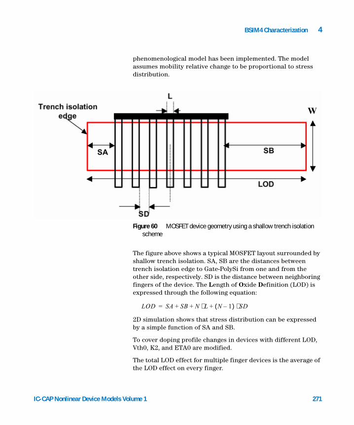
BSIM4 Characterization 4
IC-CAP Nonlinear Device Models Vo
phenomenological model has been implemented. The model assumes mobility relative change to be proportional to stress distribution.
The figure above shows a typical MOSFET layout surrounded by shallow trench isolation. SA, SB are the distances between trench isolation edge to Gate-PolySi from one and from the other side, respectively. SD is the distance between neighboring fingers of the device. The Length of Oxide Definition (LOD) is expressed through the following equation:
2D simulation shows that stress distribution can be expressed by a simple function of SA and SB.
To cover doping profile changes in devices with different LOD, Vth0, K2, and ETA0 are modified.
The total LOD effect for multiple finger devices is the average of the LOD effect on every finger.
Figure 60 MOSFET device geometry using a shallow trench isolation scheme
W
LOD SA SB N L N 1–( ) SD⋅+⋅+ +=
lume 1 271
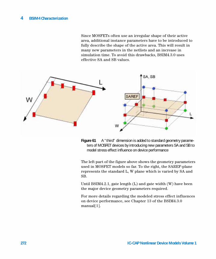
272
4 BSIM4 Characterization
Since MOSFETs often use an irregular shape of their active area, additional instance parameters have to be introduced to fully describe the shape of the active area. This will result in many new parameters in the netlists and an increase in simulation time. To avoid this drawbacks, BSIM4.3.0 uses effective SA and SB values.
The left part of the figure above shows the geometry parameters used in MOSFET models so far. To the right, the SAREF-plane represents the standard L, W plane which is varied by SA and SB.
Until BSIM4.2.1, gate length (L) and gate width (W) have been the major device geometry parameters required.
For more details regarding the modeled stress effect influences on device performance, see Chapter 13 of the BSIM4.3.0 manual[1].
Figure 61 A “third” dimension is added to standard geometry parame-ters of MOSFET devices by introducing new parameters SA and SB to model stress effect influence on device performance
IC-CAP Nonlinear Device Models Volume 1
BSIM4 Characterization 4
CV Modeling
Capacitance Model
IC-CAP Nonlinear Device Models Vo
To accurately model MOSFET behavior, a good capacitance model considering intrinsic and extrinsic (overlap/fringing) capacitances is important.
BSIM4 provides three options to select different capacitance models. These are the models from BSIM3v3.2, which are taken without changes. There is only one exception: Different parameters for source and drain sides are introduced, which are used to precisely model different doping concentrations and so on.
The model flag CAPMOD allows three values. CAPMOD = 0 uses piece-wise and simple equations, whereas with CAPMOD = 1 and 2 uses smooth and single equation models.
For CAPMOD = 0, VTH is taken from a long-channel device; for CAPMOD = 1 and 2, VTH is consistent with the BSIM4 DC model.
The overlap capacitance model uses a bias-independent part to model the effective overlap capacitance between gate and heavily doped source/drain regions and a gate-bias dependent part between the gate and the lightly doped source/drain regions.
Fringing capacitances between gate and source as well as gate and drain are modeled bias-independent.
Intrinsic Capacitance Modeling
All capacitances in Intrinsic Capacitance Model formulations are derived from terminal charges instead of terminal voltages to ensure charge conservation.
Long channel device models assume the mobility to be constant and no channel length modulation occurs. However, with shrinking device dimensions, velocity saturation and channel length modulation are to be considered to accurately model device behavior.
lume 1 273
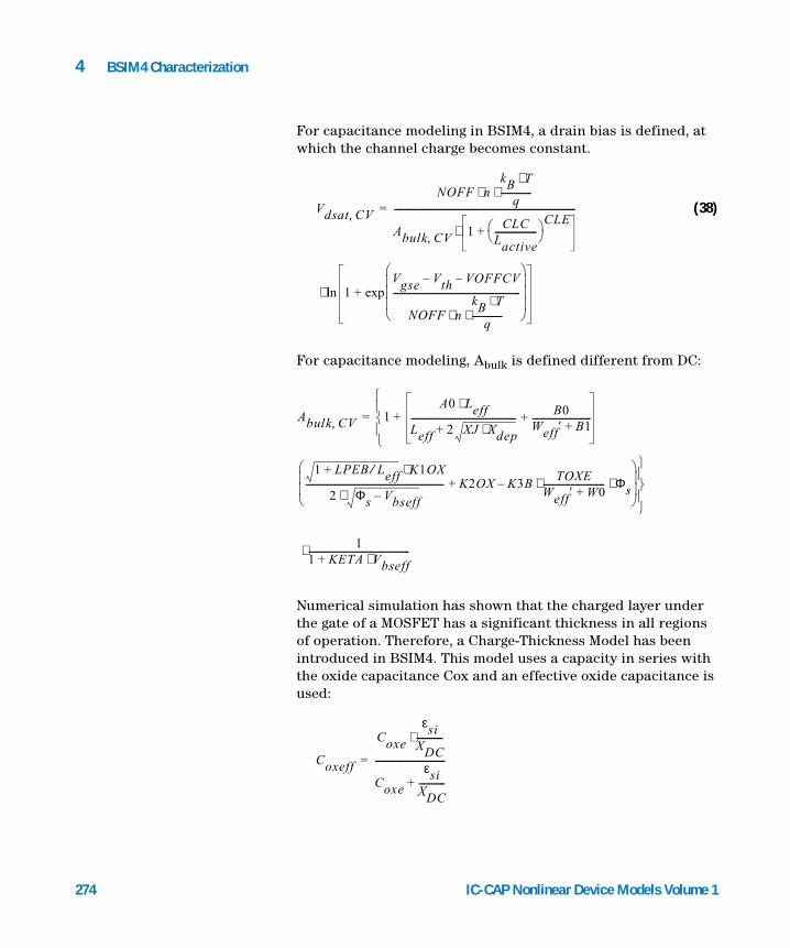
274
4 BSIM4 Characterization
For capacitance modeling in BSIM4, a drain bias is defined, at which the channel charge becomes constant.
(38)
For capacitance modeling, Abulk is defined different from DC:
Numerical simulation has shown that the charged layer under the gate of a MOSFET has a significant thickness in all regions of operation. Therefore, a Charge-Thickness Model has been introduced in BSIM4. This model uses a capacity in series with the oxide capacitance Cox and an effective oxide capacitance is used:
Vdsat CV,
NOFF nkB T⋅
q--------------⋅ ⋅
Abulk CV, 1 CLCLactive------------------- CLE
+⋅
-----------------------------------------------------------------------------------
1Vgse Vth– VOFFCV–
NOFF nkB T⋅
q--------------⋅ ⋅
----------------------------------------------------------
exp+ln⋅
=
Abulk CV, 1A0 Leff⋅
Leff 2 XJ Xdep⋅+------------------------------------------------ B0
Weff′ B1+---------------------------+
1 LPEB Leff⁄+ K1OX⋅
2 Φs Vbseff–⋅--------------------------------------------------------------- K2OX K3B
TOXEWeff ′ W0+---------------------------- Φs⋅ ⋅–+
+
11 KETA Vbseff⋅+----------------------------------------------⋅
=
Coxeff
Coxe
εsiXDC------------⋅
Coxe
εsiXDC------------+
--------------------------------=
IC-CAP Nonlinear Device Models Volume 1
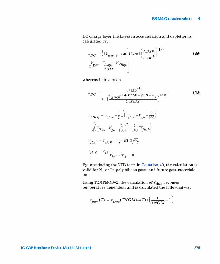
BSIM4 Characterization 4
IC-CAP Nonlinear Device Models Vo
DC charge layer thickness in accumulation and depletion is calculated by:
(39)
whereas in inversion
(40)
By introducing the VFB term in Equation 40, the calculation is valid for N+ or P+ poly-silicon gates and future gate materials too.
Using TEMPMOD=2, the calculation of Vfbzb becomes temperature dependent and is calculated the following way:
XDC13--- Ldebye ACDE
NDEP
2 1016⋅
------------------- 1 4⁄–
Vgse Vbseff– VFBeff–
TOXE-----------------------------------------------------------
⋅
⋅
exp⋅ ⋅=
XDC19 10
10–⋅
1Vgsteff 4 VTH0 VFB Φs––( )+
2 TOXP⋅-------------------------------------------------------------------------------
7 10⁄+
-----------------------------------------------------------------------------------------------------------=
VFBeff Vfbzb12--- Vfbzb Vgb–
2100---------–
Vfbzb Vgb–2
100---------–
2 8
100--------- Vfbzb⋅++
⋅–=
Vfbzb Vth 0, ΦS– K1 ΦS⋅–=
Vth 0, VthVbsandVds 0=
=
Vfbzb T( ) Vfbzb TNOM( ) KT1T
TNOM----------------- 1– ⋅–=
lume 1 275

4 BSIM4 Characterization
Intrinsic Capacitance Model Equations
276
There are three intrinsic capacitance models to choose from using the model flag CAPMOD. Additionally, there are three charge partitioning schemes: 40/60, 50/50, and 0/100. Those schemes describe distribution of the intrinsic capacitance charges between drain and source side.
The exact formulations for the different operation regimes and charge partitioning schemes are in the UC Berkeley manual [1] on pages 7-13 to 7-19.
Fringing Capacitance Models
The fringing capacitance consists of a bias-independent outer fringing capacitance and an inner fringing capacitance, bias-dependent. The outer fringing capacitance is modeled in BSIM4 (if not given) through:
(41)
The inner capacitance is not modeled.
CF2 EPSROX ε0⋅ ⋅
π----------------------------------------- 1
4 107–⋅
TOXE-------------------+
log⋅=
Overlap Capacitance Model
For accurate simulation results, especially the drain side overlap capacitance has to be modeled exactly because the influence of this capacitance is amplified by the gain of the transistor (Miller effect). Formerly used capacitance models assume a bias -independent overlap capacitance. However, experimental data show a gate-bias dependent overlap capacitance, which is invoked using CAPMOD = 1 or 2. Using CAPMOD = 0, a simple bias-independent model is invoked.
For CAPMOD = 0, the overlap charges are expressed by:
Gate-to-source overlap charge:
Gate-to-drain overlap charge:
Qoverlap s, Wactive CGSO Vgs⋅ ⋅=
IC-CAP Nonlinear Device Models Volume 1
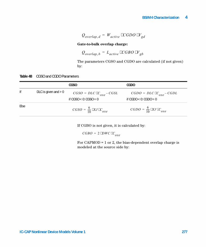
BSIM4 Characterization 4
IC-CAP Nonlinear Device Models Vo
Gate-to-bulk overlap charge:
The parameters CGSO and CGDO are calculated (if not given) by:
Qoverlap d, Wactive CGDO Vgd⋅ ⋅=
Qoverlap b, Lactive CGBO Vgb⋅ ⋅=
Table 48 CGSO and CGDO Parameters
CGSO CGDO
If DLC is given and > 0
if CGSO < 0: CGSO = 0 if CGDO < 0: CGDO = 0
Else
CGSO DLC Coxe CGSL–⋅= CGDO DLC Coxe CGDL–⋅=
CGSO6
10------ XJ Coxe⋅ ⋅= CGDO
610------ XJ Coxe⋅ ⋅=
If CGBO is not given, it is calculated by:For CAPMOD = 1 or 2, the bias-dependent overlap charge is modeled at the source side by:
CGBO 2 DWC Coxe⋅ ⋅=
lume 1 277
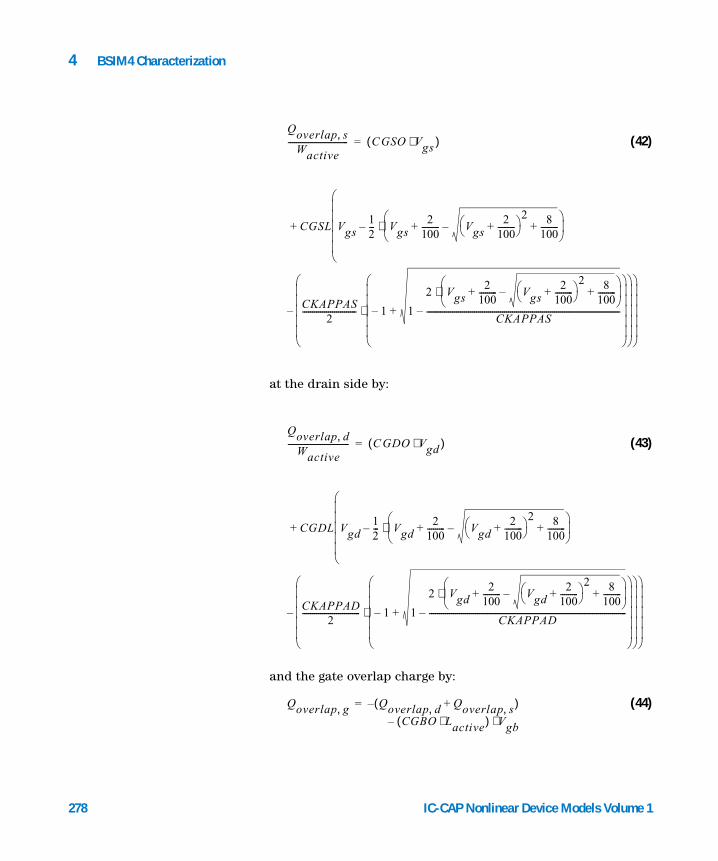
278
4 BSIM4 Characterization
(42)
at the drain side by:
(43)
and the gate overlap charge by:
(44)
Qoverlap s,Wactive
------------------------------ C( GSO Vgs )
CGSL Vgs12--- Vgs
2100--------- Vgs
2100---------+
2 8
100---------+–+
⋅–
CKAPPAS2
--------------------------- 1– 1
2 Vgs2
100--------- Vgs
2100---------+
2 8
100---------+–+
⋅
CKAPPAS-------------------------------------------------------------------------------------------------–+
⋅
–
+
⋅=
Qoverlap d,Wactive
------------------------------- C( GDO Vgd )
CGDL Vgd12--- Vgd
2100--------- Vgd
2100---------+
2 8
100---------+–+
⋅–
CKAPPAD2
----------------------------- 1– 1
2 Vgd2
100--------- Vgd
2100---------+
2 8
100---------+–+
⋅
CKAPPAD---------------------------------------------------------------------------------------------------–+
⋅
–
+
⋅=
Qoverlap g, Qoverlap d, Qoverlap s,+( )CGBO Lactive⋅( ) Vgb⋅–
–=
IC-CAP Nonlinear Device Models Volume 1

BSIM4 Characterization 4
Table 49 Intrinsic Capacitance Model Parameters
Equation Variable
BSIM4 Parameter
Description Default Value
NOFF NOFF CV parameter in Vgsteff,CV for weak to strong inversion 1.0
VOFFCV VOFFCV CV parameter in Vgsteff,CV for weak to strong inversion 0.0 V
ACDE ACDE Exponential coefficient for charge thickness in accumulation and depletion regions in CAPMOD=2
1.0 m/V
CKAPPAS CKAPPAS Coefficient of bias-dependent overlap capacitance on source side
0.6 V
CKAPPAD CKAPPAD Coefficient of bias-dependent overlap capacitance on drain side
CKAPPAS
CLC CLC Constant term for the short channel model 0.1E-7 m
CLE CLE Exponential term for the short channel model 0.6
IC-CAP Nonlinear Device Models Volume 1 279
4 BSIM4 Characterization
Structure of the BSIM4 RF Simulation Model
280
The BSIM4 model consists of some major features that make it ideal for use in real high frequency simulations. It contains:
• scalable gate resistance
• dedicated thermal noise model formulation
• different device layouts (multifinger devices) are taken into account
• substrate resistance network with correct connection to the main transistor through parasitic diodes
• New in BSIM4.3.0: Horseshoe substrate contacts
While the first three effects are fully scalable, which means the influence of the device dimensions like gate length or width is already included in the model formulation, the substrate resistance effect included into BSIM4 has not included any of this information up to version 4.3.0. To specify the substrate resistance effect, only fixed values for up to 5 different resistors could have been set. However, in reality, the substrate resistance effect depends on sheet resistance of the body, number of gate fingers and width of the devices.
Due to this shortcoming, it is not possible to generate one fully scalable model card for a family of typical RF multifinger transistors. This is the reason why the BSIM4 Modeling Package includes two different approaches for generating BSIM4 RF models:
• Single transistor models describe the very classic approach, where one simulation model is generated for each available test device. A design library based on such models does not enable the circuit designer to modify major device dimensions. Only available devices can be used to design circuits. A major benefit of this approach is that the accuracy of such a model may be very high because only one certain device behavior has to be fitted by the model parameters.
IC-CAP Nonlinear Device Models Volume 1
BSIM4 Characterization 4
IC-CAP Nonlinear Device Models Vo
• Scalable transistor models cover a certain range of major device dimensions. In the case of a RF MOS transistor, these are the gate length and gate width of a single transistor finger and the number of gate fingers. These models have a structure, such that a design engineer can change the parameters to get an optimum transistor behavior for a certain application.
In BSIM4.3.0, there is a newly introduced enhancement to modeling the substrate resistance. To take care of different geometric layouts, a so called “horseshoe” contact geometry was added (see details below inside the paragraph about “Substrate contact resistance scaling” on page 286).
The following two sections describe the structure of the single and the scalable model approaches. At first, the general structure of the BSIM4 RF model is shown.
lume 1 281
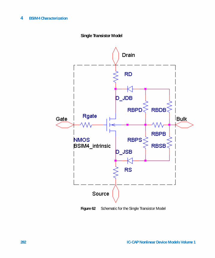
282
4 BSIM4 Characterization
Single Transistor Model
Figure 62 Schematic for the Single Transistor Model
IC-CAP Nonlinear Device Models Volume 1
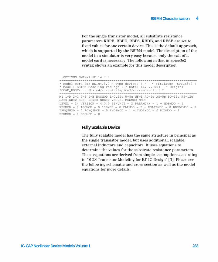
BSIM4 Characterization 4
IC-CAP Nonlinear Device Models Vo
For the single transistor model, all substrate resistance parameters RBPB, RBPD, RBPS, RBDB, and RBSB are set to fixed values for one certain device. This is the default approach, which is supported by the BSIM4 model. The description of the model in a simulator is very easy because only the call of a model card is necessary. The following netlist in spice3e2 syntax shows an example for this model description:
GMIN=1.0E-14 * *
.OPTIONS ----------------------------------------------------------------------- * Model card for BSIM4.3.0 n-type devices | * | * Simulator: SPICE3e2 | * Model: BSIM4 Modeling Package | * Date: 16.07.2004 | * Origin: ICCAP_ROOT/..../bsim4/circuits/spice3/cir/nmos.cir | * ----------------------------------------------------------------------- M1 1=D 2=G 3=S 4=B MOSMOD L=0.25u W=5u NF=1 AD=5p AS=5p PD=12u PS=12u SA=0 SB=0 SD=0 NRD=0 NRS=0 .MODEL MOSMOD NMOS LEVEL = 14 VERSION = 4.3.0 BINUNIT = 2 PARAMCHK = 1 + MOBMOD = 1 RDSMOD = 0 IGCMOD = 0 IGBMOD = 0 CAPMOD = 2 + RGATEMOD = 0 RBODYMOD = 0 TRNQSMOD = 0 ACNQSMOD = 0 FNOIMOD = 1 + TNOIMOD = 0 DIOMOD = 1 PERMOD = 1 GEOMOD = 0Fully Scalable Device
The fully scalable model has the same structure in principal as the single transistor model, but uses additional, scalable, external inductors and capacitors. It uses equations to determine the values for the substrate resistance parameters. These equations are derived from simple assumptions according to “MOS Transistor Modeling for RF IC Design” [3]. Please see the following schematic and cross section as well as the model equations for more details.
lume 1 283
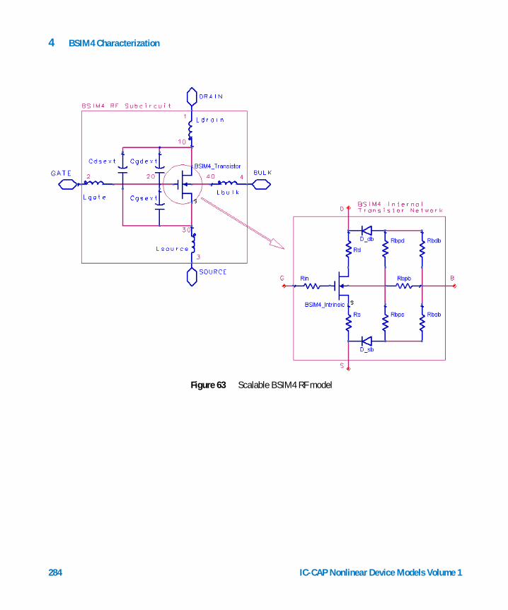
284
4 BSIM4 Characterization
Figure 63 Scalable BSIM4 RF model
IC-CAP Nonlinear Device Models Volume 1
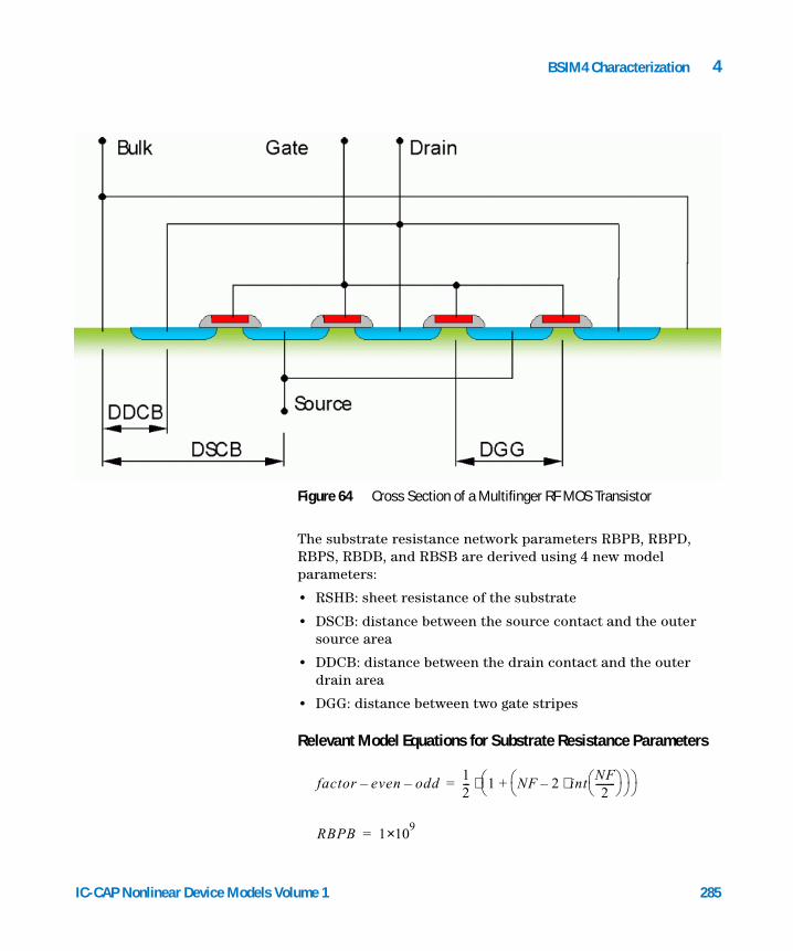
BSIM4 Characterization 4
IC-CAP Nonlinear Device Models Vo
The substrate resistance network parameters RBPB, RBPD, RBPS, RBDB, and RBSB are derived using 4 new model parameters:
• RSHB: sheet resistance of the substrate
• DSCB: distance between the source contact and the outer source area
• DDCB: distance between the drain contact and the outer drain area
• DGG: distance between two gate stripes
Relevant Model Equations for Substrate Resistance Parameters
Figure 64 Cross Section of a Multifinger RF MOS Transistor
factor even– odd–12--- 1 NF 2 int
NF2
--------
⋅–
+ ⋅=
RBPB 19×10=
lume 1 285
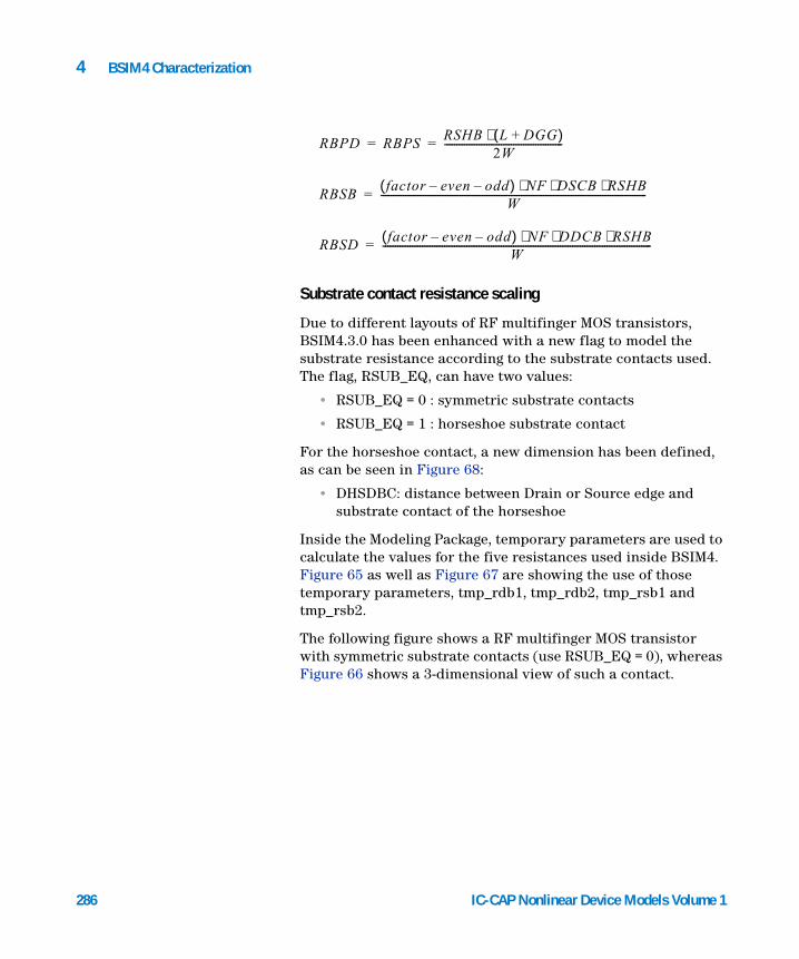
286
4 BSIM4 Characterization
Substrate contact resistance scaling
Due to different layouts of RF multifinger MOS transistors, BSIM4.3.0 has been enhanced with a new flag to model the substrate resistance according to the substrate contacts used. The flag, RSUB_EQ, can have two values:
• RSUB_EQ = 0 : symmetric substrate contacts
• RSUB_EQ = 1 : horseshoe substrate contact
For the horseshoe contact, a new dimension has been defined, as can be seen in Figure 68:
• DHSDBC: distance between Drain or Source edge and substrate contact of the horseshoe
Inside the Modeling Package, temporary parameters are used to calculate the values for the five resistances used inside BSIM4. Figure 65 as well as Figure 67 are showing the use of those temporary parameters, tmp_rdb1, tmp_rdb2, tmp_rsb1 and tmp_rsb2.
The following figure shows a RF multifinger MOS transistor with symmetric substrate contacts (use RSUB_EQ = 0), whereas Figure 66 shows a 3-dimensional view of such a contact.
RBPD RBPSRSHB L DGG+( )⋅
2W------------------------------------------------= =
RBSBfactor even– odd–( ) NF DSCB RSHB⋅ ⋅ ⋅
W------------------------------------------------------------------------------------------------------------=
RBSDfactor even– odd–( ) NF DDCB RSHB⋅ ⋅ ⋅
W-------------------------------------------------------------------------------------------------------------=
IC-CAP Nonlinear Device Models Volume 1

BSIM4 Characterization 4
IC-CAP Nonlinear Device Models Vo
Figure 65 Symmetric substrate contacts, top view
lume 1 287
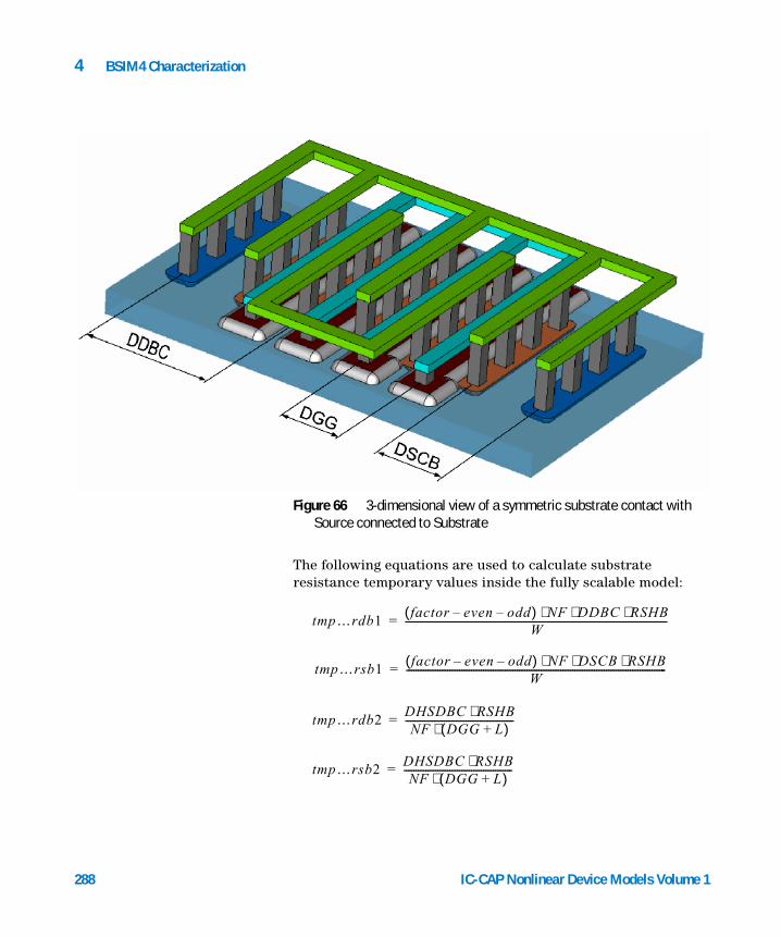
288
4 BSIM4 Characterization
The following equations are used to calculate substrate resistance temporary values inside the fully scalable model:
Figure 66 3-dimensional view of a symmetric substrate contact with Source connected to Substrate
tmp…rdb1factor even– odd–( ) NF DDBC RSHB⋅ ⋅ ⋅
W-------------------------------------------------------------------------------------------------------------=
tmp…rsb1factor even– odd–( ) NF DSCB RSHB⋅ ⋅ ⋅
W------------------------------------------------------------------------------------------------------------=
tmp…rdb2DHSDBC RSHB⋅NF DGG L+( )⋅---------------------------------------------=
tmp…rsb2DHSDBC RSHB⋅NF DGG L+( )⋅
---------------------------------------------=
IC-CAP Nonlinear Device Models Volume 1

BSIM4 Characterization 4
IC-CAP Nonlinear Device Models Vo
The following figures show the horseshoe substrate contact as well as a 3-dimensional view of such a contact (use RSUB_EQ=1).
The temporary values calculated above are combined to give BSIM4 model parameters as follows:
RSUB_EQ = 0:
Figure 67 Horseshoe substrate contacts, top view
RBDB RDB tmp…rdb1⋅=
RBSB RSB tmp…rsb1⋅=
lume 1 289
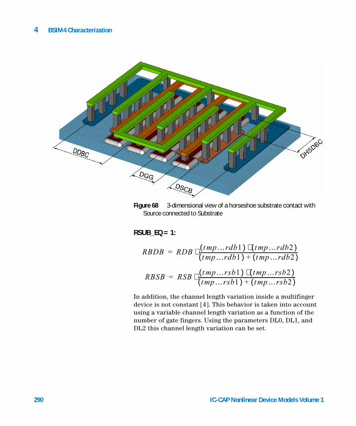
290
4 BSIM4 Characterization
RSUB_EQ = 1:
In addition, the channel length variation inside a multifinger device is not constant [4]. This behavior is taken into account using a variable channel length variation as a function of the number of gate fingers. Using the parameters DL0, DL1, and DL2 this channel length variation can be set.
Figure 68 3-dimensional view of a horseshoe substrate contact with Source connected to Substrate
RBDB RDBt( mp…rdb1 ) t( mp…rdb2 )⋅t( mp…rdb1 ) t( mp…rdb2 )+
---------------------------------------------------------------------------⋅=
RBSB RSBt( mp…rsb1 ) t( mp…rsb2 )⋅t( mp…rsb1 ) t( mp…rsb2 )+
--------------------------------------------------------------------------⋅=
IC-CAP Nonlinear Device Models Volume 1
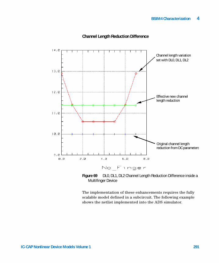
BSIM4 Characterization 4
IC-CAP Nonlinear Device Models Vo
Channel Length Reduction Difference
The implementation of these enhancements requires the fully scalable model defined in a subcircuit. The following example shows the netlist implemented into the ADS simulator.
Figure 69 DL0, DL1, DL2 Channel Length Reduction Difference inside a Multifinger Device
Channel length variation set with DL0, DL1, DL2
Effective new channel length reduction
Original channel length reduction from DC parameters
lume 1 291
292
4 BSIM4 Characterization
LINK CIRC "Circuit"datacircuitdeck ; ----------------------------------------------------------------------------------------- ; Fully scalable subcircuit model for BSIM4.5.0 RF n-type devices ; ; Simulator: Agilent Advanced Design System ; Model: BSIM4 Modeling Package ; Date: 09.02.2006 ; Origin: ICCAP_ROOT/..../bsim4/circuits/hpeesofsim/cir/rf_nmos_scale.cir ; ----------------------------------------------------------------------------------------- ; ; --- Information for model implementation ------------------------------------------------- ; In ADS, call the sub circuit model as follows with the actual values of L, W, etc. ; ; BSIM4_RF_Extract:x_rf_transistor n1 n2 n3 n4 tmp_l= 0.25u tmp_w= 80u .... ; ; Please note, that according to the BSIM4 model definition, the parameters tmp_w, tmp_ad, ; tmp_as, tmp_pd, tmp_ps, tmp_nrs, tmp_nrd always define the TOTAL width (drain area, ..., ; number of drain squares) of the multi finger device. ; The width (drain area, ..) of a single finger of the multifinger MOSFET will be calculated ; inside the BSIM4 model using the instance parameter 'NF' and the selected 'GEOMOD' parameter. ; ; define bsim4_rf_extract (i1 i2 i3 i4);--- parameters for sub-circuit ----------------------------------------------------------- parameters tmp_l= 1u tmp_w= 10e-6 tmp_nf= 1 tmp_ad= 10e-12 tmp_as= 10e-12 tmp_pd= 22e-6tmp_ps= 22e-6 tmp_sa= 0 tmp_sb= 0 tmp_sd= 0 tmp_nrd= 0 tmp_nrs= 0 ; ;--- BSIM4 model card --------------------------------------------------------------------- NMOS = 1 PMOS = 0 VERSION = 4.50 BINUNIT = 2 PARAMCHK = 1 MOBMOD = 1 RDSMOD = 0 IGCMOD = 0 IGBMOD = 0 CAPMOD = 2 RGATEMOD = 0 RBODYMOD = 0 TRNQSMOD = 0 ACNQSMOD = 0 FNOIMOD = 1 TNOIMOD = 0 DIOMOD = 1 PERMOD = 1 GEOMOD = 0 EPSROX = 3.9 TOXE = 3e-9 TOXP = 3e-9 TOXM = 3e-9 DTOX = 0 XJ = 1.5e-7 NDEP = 1.7e17 NGATE = 0 NSD = 1e20 XT = 1.55e-7 RSH = 0 RSHG = 0.1 VTH0 = 0.7 PHIN = 0 K1 = 0.33 K2 = -0.018 K3 = 2 K3B = 0 W0 = 2.5e-6 LPE0 = 1.74e-7 LPEB = 0 VBM = -3 DVT0 = 2.2 DVT1 = 0.53 DVT2 = -0.032 DVTP0 = 0 DVTP1 = 0.001 DVT0W = 0 DVT1W = 5.3e6 DVT2W = -0.032 ETA0 = 0.08 ETAB = -0.07 DSUB = 0.56 U0 = 0.067 UA = 1e-9 UB = 1e-19 UC = -0.0465 UD = 1e+14 UP = 0 LP = 1e-8 EU = 1.67 VSAT = 8e4 A0 = 1 AGS = 0 B0 = 0 B1 = 0 KETA = -0.047 A1 = 0 A2 = 1 VOFF = -0.08 VOFFL = 0 MINV = 0 NFACTOR = 1 CIT = 0 CDSC = 2.4e-4 CDSCB = 0 CDSCD = 0 PCLM = 1.3 PDIBLC1 = 0.39 PDIBLC2 = 0.0086 PDIBLCB = 0 DROUT = 0.56 PSCBE1 = 4.24e8 PSCBE2 = 1e-5 PVAG = 0 DELTA = 0.01 FPROUT = 0 PDITS = 1m PDITSL = 0 PDITSD = 0 RDSW = 200 RDSWMIN = 0 RDW = 100 RDWMIN = 0 RSW = 100 RSWMIN = 0
PRWG = 1 PRWB = 0 WR = 1 LINT = 0 WINT = 0
IC-CAP Nonlinear Device Models Volume 1
BSIM4 Characterization 4
DWG = 0 DWB = 0 WL = 0 WLN = 1 WW = 0 WWN = 1 WWL = 0 LL = 0 LLN = 1 LW = 0 LWN = 1 LWL = 0 LLC = 0 LWC = 0 LWLC = 0 WLC = 0 WWC = 0 WWLC = 0 ALPHA0 = 1e-5 ALPHA1 = 0 BETA0 = 15 AGIDL = 0 BGIDL = 2.3e9 CGIDL = 0.5 EGIDL = 0.8 AIGBACC = 0.43 BIGBACC = 0.054 CIGBACC = 0.075 NIGBACC = 1 AIGBINV = 0.35 BIGBINV = 0.03 CIGBINV = 0.006 EIGBINV = 1.1 NIGBINV = 3 AIGC = 0.54 BIGC = 0.054 CIGC = 0.075 AIGSD = 0.43 BIGSD = 0.054 CIGSD = 0.075 DLCIG = 0 NIGC = 1 POXEDGE = 1 PIGCD = 1 NTOX = 1 TOXREF = 3e-9 XPART = 0 CGSO = 0 CGDO = 0 CGBO = 0 CGSL = 0 CGDL = 0 CKAPPAS = 0.6 CKAPPAD = 0.6 CF = 0 CLC = 1e-7 CLE = 0.6 DLC = 0 DWC = 0 VFBCV = -1 NOFF = 1 VOFFCV = 0 ACDE = 1 MOIN = 15 XRCRG1 = 12 XRCRG2 = 1 RBPB = 50 RBPD = 50 RBPS = 15 RBDB = 50 RBSB = 50 GBMIN = 1e-12 RBPS0 = 50 RBPSL = 0 RBPSW = 0 RBPSNF = 0 RBPD0 = 50 RBPDL = 0 RBPDW = 0 RBPDNF = 0 RBPBX0 = 100 RBPBXL = 0 RBPBXW = 0 RBPBXNF = 0 RBPBY0 = 100 RBPBYL = 0 RBPBYW = 0 RBPBYNF = 0 RBSBX0 = 100 RBSBY0 = 100 RBDBX0 = 100 RBDBY0 = 100 RBSDBXL = 0 RBSDBXW = 0 RBSDBXNF = 0 RBSDBYL = 0 RBSDBYW = 0 RBSDBYNF = 0 NOIA = 6.25e41 NOIB = 3.125e26 NOIC = 8.75 EM = 4.1e7 AF = 1 EF = 1 KF = 0 NTNOI = 1 TNOIA = 1.5 TNOIB = 3.5 DMCG = 0 DMCI = 0 DMDG = 0 DMCGT = 0 DWJ = 0 XGW = 0 XGL = 0 NGCON = 1 XL = 0 XW = 0 IJTHSREV = 0.1 IJTHSFWD = 0.1 XJBVS = 1 BVS = 10 JSS = 1e-4 JSWS = 0 JSWGS = 0 CJS = 5e-4 MJS = 0.5 MJSWS = 0.33 CJSWS = 5e-10 CJSWGS = 5e-10 MJSWGS = 0.33 PBS = 1 PBSWS = 1 PBSWGS = 1 IJTHDREV = 0.1 IJTHDFWD = 0.1 XJBVD = 1 BVD = 10 JSD = 1e-4 JSWD = 0 JSWGD = 0 CJD = 5e-4 MJD = 0.5 MJSWD = 0.33 CJSWD = 5e-10 CJSWGD = 5e-10 MJSWGD = 0.33 PBD = 1 PBSWD = 1 PBSWGD = 1 SAREF = 1E-6 SBREF = 1E-6 WLOD = 2E-6 KU0 = 4E-6 KVSAT = 0.2 KVTH0 = -2E-8 TKU0 = 0.0 LLODKU0 = 1.1 WLODKU0 = 1.1 LLODVTH = 1.0 WLODVTH = 1.0 LKU0 = 1E-6 WKU0 = 1E-6 PKU0 = 0.0 LKVTH0 = 1.1E-6 WKVTH0 = 1.1E-6 PKVTH0 = 0.0 STK2 = 0.0 LODK2 = 1.0 STETA0 = 0.0 LODETA0 = 1.0 LAMBDA = 0 VTL = 2e5 LC = 0 XN = 3 TEMPMOD = 0 TNOM = 27 UTE = -1.5 KT1 = -0.11 KT1L = 0 KT2 = 0.022 UA1 = 1e-9 UB1 = -1e-18 UC1 = 0.067 UD1 = 0 AT = 3.3e4 PRT = 0 TVFBSDOFF= 0 TVOFF = 0 NJS = 1 NJD = 1 XTIS = 3 XTID = 3 TPB = 0 TPBSW = 0 TPBSWG = 0 TCJ = 0 TCJSW = 0 TCJSWG = 0 JTSS = 0 JTSD = 0 JTSSWS = 0 JTSSWD = 0 JTSSWGS = 0 JTSSWGD = 0 NJTS = 20.0 NJTSSW = 20 NJTSSWG = 20 VTSS = 10 VTSD = 10 VTSSWS = 10 VTSSWD = 10 VTSSWGS = 10 VTSSWGD = 10 XTSS = 0.02 XTSD = 0.02 XTSSWS = 0.02 XTSSWD = 0.02 XTSSWGS = 0.02 XTSSWGD = 0.02 TNJTS = 0 TNJTSSW = 0 TNJTSSWG= 0 LINTNOI = 0 VFBSDOFF = 0.0 WEB = 0 WEC = 0 KVTH0WE = 0 K2WE = 0 KU0WE = 0 SCREF = 1E-6 WPEMOD = 0 ;; model bsim4_mos BSIM4 \ NMOS = NMOS PMOS = PMOS \ Version = VERSION Binunit = BINUNIT Paramchk = PARAMCHK \ Mobmod = MOBMOD Rdsmod = RDSMOD Igcmod = IGCMOD Igbmod = IGBMOD \ Capmod = CAPMOD Rgatemod = RGATEMOD Rbodymod = RBODYMOD Trnqsmod = TRNQSMOD \
Acnqsmod = ACNQSMOD Fnoimod = FNOIMOD Tnoimod = TNOIMOD Diomod = DIOMOD \ Permod = PERMOD Geomod = GEOMOD Epsrox = EPSROX Toxe = TOXE \ Toxp = TOXP Toxm = TOXM Dtox = DTOX Xj = XJ \ Ndep = NDEP Ngate = NGATE Nsd = NSD Xt = XT \ Rsh = RSH Rshg = RSHG Vth0 = VTH0 Phin = PHIN \ K1 = K1 K2 = K2 K3 = K3 K3b = K3B \
IC-CAP Nonlinear Device Models Volume 1 293
4 BSIM4 Characterization
W0 = W0 Lpe0 = LPE0 Lpeb = LPEB Vbm = VBM \ Dvt0 = DVT0 Dvt1 = DVT1 Dvt2 = DVT2 Dvtp0 = DVTP0 \ Dvtp1 = DVTP1 Dvt0w = DVT0W Dvt1w = DVT1W Dvt2w = DVT2W \ Eta0 = ETA0 Etab = ETAB Dsub = DSUB U0 = U0 \ Ua = UA Ub = UB Uc = UC Ud = UD \ Up = UP Lp = LP Eu = EU Vsat = VSAT \ A0 = A0 Ags = AGS B0 = B0 B1 = B1 \Keta = KETA A1 = A1 A2 = A2 Voff = VOFF \Voffl = VOFFL Minv = MINV Nfactor = NFACTOR Cit = CIT \Cdsc = CDSC Cdscb = CDSCB Cdscd = CDSCD Pclm = PCLM \Pdiblc1 = PDIBLC1 Pdiblc2 = PDIBLC2 Pdiblcb = PDIBLCB Drout = DROUT \Pscbe1 = PSCBE1 Pscbe2 = PSCBE2 Pvag = PVAG Delta = DELTA \Fprout = FPROUT Pdits = PDITS Pditsl = PDITSL Pditsd = PDITSD \Rdsw = RDSW Rdswmin = RDSWMIN Rdw = RDW Rdwmin = RDWMIN \Rsw = RSW Rswmin = RSWMIN Prwg = PRWG Prwb = PRWB \Wr = WR Lint = LINT Wint = WINT Dwg = DWG \Dwb = DWB Wl = WL Wln = WLN Ww = WW \Wwn = WWN Wwl = WWL Ll = LL Lln = LLN \Lw = LW Lwn = LWN Lwl = LWL Llc = LLC \Lwc = LWC Lwlc = LWLC Wlc = WLC Wwc = WWC \Wwlc = WWLC \Alpha0 = ALPHA0 Alpha1 = ALPHA1 Beta0 = BETA0 \Agidl = AGIDL Bgidl = BGIDL Cgidl = CGIDL Egidl = EGIDL \Aigbacc = AIGBACC Bigbacc = BIGBACC Cigbacc = CIGBACC Nigbacc = NIGBACC \Aigbinv = AIGBINV Bigbinv = BIGBINV Cigbinv = CIGBINV Eigbinv = EIGBINV \Nigbinv = NIGBINV Aigc = AIGC Bigc = BIGC Cigc = CIGC \Aigsd = AIGSD Bigsd = BIGSD Cigsd = CIGSD Dlcig = DLCIG \Nigc = NIGC Poxedge = POXEDGE Pigcd = PIGCD Ntox = NTOX \Toxref = TOXREF \Xpart = XPART Cgso = CGSO Cgdo = CGDO Cgbo = CGBO \Cgsl = CGSL Cgdl = CGDL Ckappas = CKAPPAS Ckappad = CKAPPAD \Cf = CF Clc = CLC Cle = CLE Dlc = DLC \Dwc = DWC Vfbcv = VFBCV Noff = NOFF Voffcv = VOFFCV \Acde = ACDE Moin = MOIN \Xrcrg1 = XRCRG1 Xrcrg2 = XRCRG2 Rbpb = RBPB Rbpd = RBPD \Rbps = RBPS \Rbdb = RBDB Rbsb = RBSB Gbmin = GBMIN \Rbps0 = RBPS0 Rbpsl = RBPSL Rbpsw = RBPSW Rbpsnf = RBPSNF \Rbpd0 = RBPD0 Rbpdl = RBPDL Rbpdw = RBPDW Rbpdnf = RBPDNF \Rbpbx0 = RBPBX0 Rbpbxl = RBPBXL Rbpbxw = RBPBXW Rbpbxnf = RBPBXNF \Rbpby0 = RBPBY0 Rbpbyl = RBPBYL Rbpbyw = RBPBYW Rbpbynf = RBPBYNF \Rbsbx0 = RBSBX0 Rbsby0 = RBSBY0 Rbdbx0 = RBDBX0 Rbdby0 = RBDBY0 \Rbsdbxl = RBSDBXL Rbsdbxw = RBSDBXW Rbsdbxnf = RBSDBXNF \Rbsdbyl = RBSDBYL Rbsdbyw = RBSDBYW Rbsdbynf = RBSDBYNF \Noia = NOIA Noib = NOIB Noic = NOIC Em = EM \Af = AF Ef = EF Kf = KF Ntnoi = NTNOI \Tnoia = TNOIA Tnoib = TNOIB \Dmcg = DMCG Dmci = DMCI Dmdg = DMDG Dmcgt = DMCGT \Dwj = DWJ Xgw = XGW Xgl = XGL Ngcon = NGCON \Xl = XL Xw = XW \Ijthsrev = IJTHSREV Ijthsfwd = IJTHSFWD Xjbvs = XJBVS Bvs = BVS \Jss = JSS Jsws = JSWS Jswgs = JSWGS Cjs = CJS \Mjs = MJS Mjsws = MJSWS Cjsws = CJSWS Cjswgs = CJSWGS \Mjswgs = MJSWGS Pbs = PBS Pbsws = PBSWS Pbswgs = PBSWGS \Ijthdrev = IJTHDREV Ijthdfwd = IJTHDFWD Xjbvd = XJBVD Bvd = BVD \Jsd = JSD Jswd = JSWD Jswgd = JSWGD Cjd = CJD \Mjd = MJD Mjswd = MJSWD Cjswd = CJSWD Cjswgd = CJSWGD \
294 IC-CAP Nonlinear Device Models Volume 1

BSIM4 Characterization 4
IC-CAP Nonlinear Device Models Vo
PBD Pbswd = PBSWD Pbswgd = PBSWGD \
Mjswgd = MJSWGD Pbd =Saref = SAREF Sbref = SBREF Wlod = WLOD Ku0 = KU0 \Kvsat = KVSAT Kvth0 = KVTH0 Tku0 = TKU0 Llodku0 = LLODKU0 \Wlodku0 = WLODKU0 Llodvth = LLODVTH Wlodvth = WLODVTH Lku0 = LKU0 \Wku0 = WKU0 Pku0 = PKU0 Lkvth0 = LKVTH0 Wkvth0 = WKVTH0 \Pkvth0 = PKVTH0 Stk2 = STK2 Lodk2 = LODK2 Steta0 = STETA0 \Lodeta0 = LODETA0 Lambda = LAMBDA Vtl = VTL Lc = LC \Xn = XN \Tempmod = TEMPMOD \Tnom = TNOM Ute = UTE Kt1 = KT1 Kt1l = KT1L \Kt2 = KT2 Ua1 = UA1 Ub1 = UB1 Uc1 = UC1 \Ud1 = UD1 At = AT Prt = PRT Tvfbsdoff= TVFBSDOFF \Tvoff = TVOFF Njs = NJS Njd = NJD Xtis = XTIS \Xtid = XTID Tpb = TPB Tpbsw = TPBSW Tpbswg = TPBSWG \Tcj = TCJ Tcjsw = TCJSW Tcjswg = TCJSWG Jtss = JTSS \Jtsd = JTSD Jtssws = JTSSWS Jtsswd = JTSSWD Jtsswgs = JTSSWGS \Jtsswgd = JTSSWGD Njts = NJTS Njtssw = NJTSSW Njtsswg = NJTSSWG \Vtss = VTSS Vtsd = VTSD Vtssws = VTSSWS Vtsswd = VTSSWD \Vtsswgs = VTSSWGS Vtsswgd = VTSSWGD Xtss = XTSS Xtsd = XTSD \Xtssws = XTSSWS Xtsswd = XTSSWD Xtsswgs = XTSSWGS Xtsswgd = XTSSWGD \Tnjts = TNJTS Tnjtssw = TNJTSSW Tnjtsswg = TNJTSSWG Lintnoi = LINTNOI \Vfbsdoff = VFBDSDOFF Web = WEB Wec = WEC Kvth0we = KVTH0WE \K2we = K2WE Ku0we = KU0WE Scref = SCREF Wpemod = WPEMOD ;;;--- Extension to BSIM4 to enable: -----------------------------------------; - scalable external capacitors taking into account cross coupling between metal lines and ; inductors to account for delay effects due to the size of the devices; - scalable channel length reduction in multi finger devices; - a scalable substrate network using different configurations (symmetric / horseshoe); - scalable Delta L reduction;CGDEXT0 = 1e-9 ; external capacitance gate - drain per gate width and gate finger [F/m]CGSEXT0 = 1e-9 ; external capacitance gate - source per gate width and gate finger [F/m]CDSEXT0 = 1e-9 ; external capacitance drain - source per gate width and gate finger [F/m]LDRAIN0 = 1e-6 ; drain inductance per gate width and gate finger [H/m]LGATE0 = 1e-6 ; gate inductance per gate width and gate finger [H/m]LSOURCE0 = 1e-6 ; source inductance per gate width and gate finger [H/m]LBULK0 = 1e-6 ; bulk inductance per gate width and gate finger [H/m]RSHB = 25 ; bulk sheet resistance [Ohms sq]DSBC = 2e-6 ; distance source implant to bulk contact [m]DDBC = 2e-6 ; distance drain implant to bulk contact [m]DGG = 2e-6 ; distance gate to gate [m]DHSDBC = 2e-6 ; distance drain/source edge to horseshoe substrate contact [m]DL0 = 0 ; basic channel length reduction correction [m]DL1 = 0 ; channel length reduction correction 1. and 2. outer fingers [m]DL2 = 0 ; channel length reduction correction outer fingers [m]RSUBEQ = 0 ; selection flag for different substrate resistance configurations [-]
; RSUBEQ= 0: symmetric substrate resistance contacts; RSUBEQ= 1: horseshoe substrate resistance contacts
;
lume 1 295
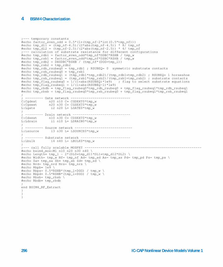
4 BSIM4 Characterization
;--- temporary constants#echo factor_even_odd = 0.5*(1+(tmp_nf-2*int(0.5*tmp_nf))) #echo tmp_dl1 = (tmp_nf-4.5)/(2*abs(tmp_nf-4.5)) * 8/ tmp_nf#echo tmp_dl2 = (tmp_nf-2.5)/(2*abs(tmp_nf-2.5)) * 4/ tmp_nf;--- calculation of substrate resistance for different configurations#echo tmp_rdb1 = factor_even_odd*tmp_nf*DDBC*RSHB / tmp_w#echo tmp_rsb1 = factor_even_odd*tmp_nf*DSBC*RSHB / tmp_w#echo tmp_rdb2 = DHSDBC*RSHB / (tmp_nf*(DGG+tmp_l))#echo tmp_rsb2 = tmp_rdb2#echo tmp_rdb_rsubeq0 = tmp_rdb1 ; RSUBEQ= 0 symmetric substrate contacts#echo tmp_rsb_rsubeq0 = tmp_rsb1#echo tmp_rdb_rsubeq1 = (tmp_rdb1*tmp_rdb2)/(tmp_rdb1+tmp_rdb2) ; RSUBEQ= 1 horseshoe #echo tmp_rsb_rsubeq1 = (tmp_rsb1*tmp_rsb2)/(tmp_rsb1+tmp_rsb2) ; substrate contacts#echo tmp_flag_rsubeq0 = 1/(1+abs(RSUBEQ)*1e9) ; flag to select substrate equations#echo tmp_flag_rsubeq1 = 1/(1+abs(RSUBEQ-1)*1e9)#echo tmp_rbdb = tmp_flag_rsubeq0*tmp_rdb_rsubeq0 + tmp_flag_rsubeq1*tmp_rdb_rsubeq1#echo tmp_rbsb = tmp_flag_rsubeq0*tmp_rsb_rsubeq0 + tmp_flag_rsubeq1*tmp_rsb_rsubeq1;; --------- Gate network ------------------------------C:Cgdext n20 n10 C= CGDEXT0*tmp_wC:Cgsext n20 n30 C= CGSEXT0*tmp_wL:Lgate i2 n20 L= LGATE0*tmp_w;; --------- Drain network -----------------------------C:Cdsext n10 n30 C= CDSEXT0*tmp_wL:Ldrain i1 n10 L= LDRAIN0*tmp_w;; --------- Source network -----------------------------L:Lsource i3 n30 L= LSOURCE0*tmp_w;; --------- Substrate network -------------------------L:Lbulk i4 n40 L= LBULK0*tmp_w;;--- call fully scalable MOSFET -----------------------------------------------------------#echo bsim4_mos:M1 n10 n20 n30 n40 \#echo Length= tmp_l - 2*(DL0+tmp_dl1*DL1+tmp_dl2*DL2) \#echo Width= tmp_w Nf= tmp_nf Ad= tmp_ad As= tmp_as Pd= tmp_pd Ps= tmp_ps \#echo Sa= tmp_sa Sb= tmp_sb Sd= tmp_sd \#echo Nrd= tmp_nrd Nrs= tmp_nrs \#echo Rbpb= 1e9 \#echo Rbps= 0.5*RSHB*(tmp_l+DGG) / tmp_w \#echo Rbpd= 0.5*RSHB*(tmp_l+DGG) / tmp_w \#echo Rbsb= tmp_rbsb \#echo Rbdb= tmp_rbdb;end BSIM4_RF_Extract
296 IC-CAP Nonlinear Device Models Volume 1

BSIM4 Characterization 4
Test Structures for Deep Submicron CMOS Processes
IC-CAP Nonlinear Device Models Vo
A very important prerequisite for a proper model parameter extraction is the selection of appropriate test structures.
Chapter 5, “BSIM3v3 Characterization” contains detailed descriptions of appropriate test structures for deep submicron MOS transistors. See Table 66 on page 425 for an example.
A detailed description of ideal test structures is located in the JESSI AC-41 reports [2].
lume 1 297
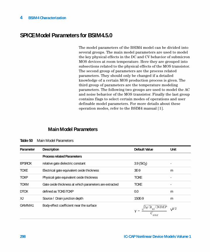
4 BSIM4 Characterization
SPICE Model Parameters for BSIM4.5.0
298
The model parameters of the BSIM4 model can be divided into several groups. The main model parameters are used to model the key physical effects in the DC and CV behavior of submicron MOS devices at room temperature. Here they are grouped into subsections related to the physical effects of the MOS transistor. The second group of parameters are the process related parameters. They should only be changed if a detailed knowledge of a certain MOS production process is given. The third group of parameters are the temperature modeling parameters. The following two groups are used to model the AC and noise behavior of the MOS transistor. Finally the last group contains flags to select certain modes of operations and user definable model parameters. For more details about these operation modes, refer to the BSIM4 manual [1].
Main Model Parameters
Table 50 Main Model Parameters
Parameter Description Default Value Unit
Process related Parameters
EPSROX relative gate dielectric constant 3.9 (SiO2) -
TOXE Electrical gate equivalent oxide thickness 3E-9 m
TOXP Physical gate equivalent oxide thickness TOXE -
TOXM Gate oxide thickness at which parameters are extracted TOXE -
DTOX defined as TOXE-TOXP 0.0 m
XJ Source / Drain junction depth 150E-9 m
GAMMA1 Body-effect coefficient near the surfaceV1/2
γ2q εsi NDEP⋅ ⋅
Coxe-------------------------------------------=
IC-CAP Nonlinear Device Models Volume 1
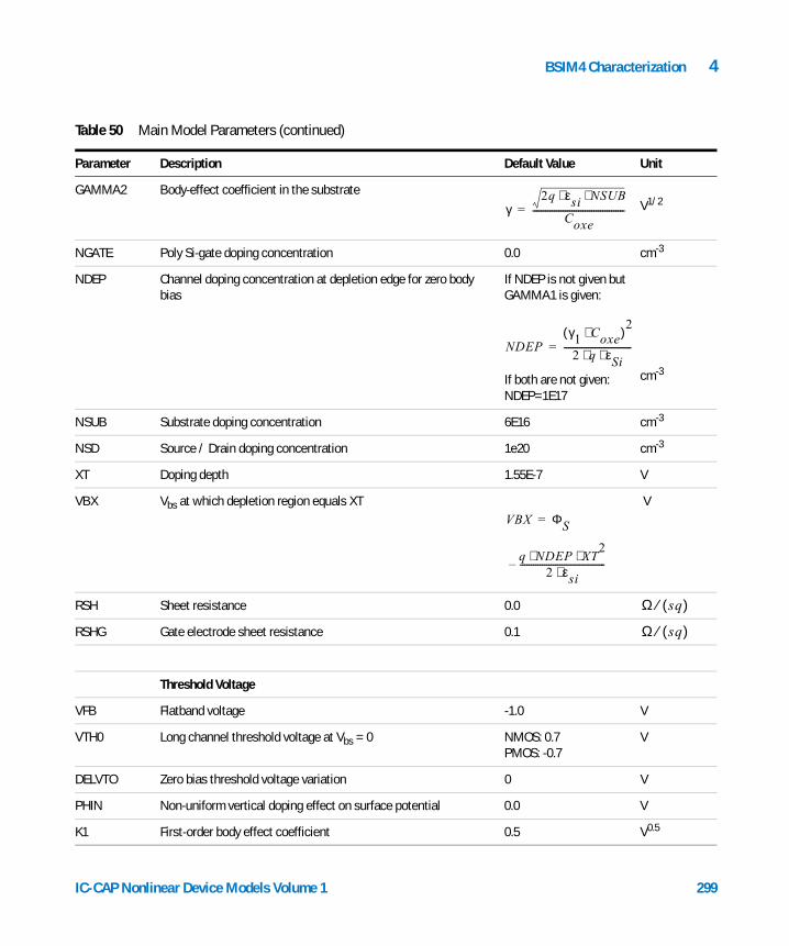
BSIM4 Characterization 4
GAMMA2 Body-effect coefficient in the substrateV1/2
NGATE Poly Si-gate doping concentration 0.0 cm-3
NDEP Channel doping concentration at depletion edge for zero body bias
If NDEP is not given but GAMMA1 is given:
If both are not given: NDEP=1E17
cm-3
NSUB Substrate doping concentration 6E16 cm-3
NSD Source / Drain doping concentration 1e20 cm-3
XT Doping depth 1.55E-7 V
VBX Vbs at which depletion region equals XT V
RSH Sheet resistance 0.0
RSHG Gate electrode sheet resistance 0.1
Threshold Voltage
VFB Flatband voltage -1.0 V
VTH0 Long channel threshold voltage at Vbs = 0 NMOS: 0.7PMOS: -0.7
V
DELVTO Zero bias threshold voltage variation 0 V
PHIN Non-uniform vertical doping effect on surface potential 0.0 V
K1 First-order body effect coefficient 0.5 V0.5
Table 50 Main Model Parameters (continued)
Parameter Description Default Value Unit
γ2q εsi NSUB⋅ ⋅
Coxe------------------------------------------=
NDEPγ1 Coxe⋅( )2
2 q εSi⋅ ⋅-------------------------------=
VBX ΦS
q NDEP XT2⋅ ⋅
2 εsi⋅---------------------------------------–
=
Ω sq( )⁄
Ω sq( )⁄
IC-CAP Nonlinear Device Models Volume 1 299
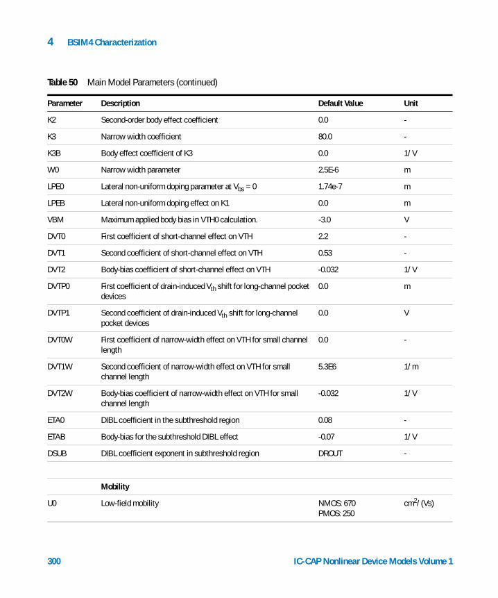
4 BSIM4 Characterization
K2 Second-order body effect coefficient 0.0 -
K3 Narrow width coefficient 80.0 -
K3B Body effect coefficient of K3 0.0 1/V
W0 Narrow width parameter 2.5E-6 m
LPE0 Lateral non-uniform doping parameter at Vbs = 0 1.74e-7 m
LPEB Lateral non-uniform doping effect on K1 0.0 m
VBM Maximum applied body bias in VTH0 calculation. -3.0 V
DVT0 First coefficient of short-channel effect on VTH 2.2 -
DVT1 Second coefficient of short-channel effect on VTH 0.53 -
DVT2 Body-bias coefficient of short-channel effect on VTH -0.032 1/V
DVTP0 First coefficient of drain-induced Vth shift for long-channel pocket devices
0.0 m
DVTP1 Second coefficient of drain-induced Vth shift for long-channel pocket devices
0.0 V
DVT0W First coefficient of narrow-width effect on VTH for small channel length
0.0 -
DVT1W Second coefficient of narrow-width effect on VTH for small channel length
5.3E6 1/m
DVT2W Body-bias coefficient of narrow-width effect on VTH for small channel length
-0.032 1/V
ETA0 DIBL coefficient in the subthreshold region 0.08 -
ETAB Body-bias for the subthreshold DIBL effect -0.07 1/V
DSUB DIBL coefficient exponent in subthreshold region DROUT -
Mobility
U0 Low-field mobility NMOS: 670 PMOS: 250
cm2/(Vs)
Table 50 Main Model Parameters (continued)
Parameter Description Default Value Unit
300 IC-CAP Nonlinear Device Models Volume 1
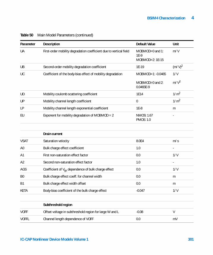
BSIM4 Characterization 4
UA First-order mobility degradation coefficient due to vertical field MOBMOD=0 and 1: 1E-9MOBMOD=2: 1E-15
m/V
UB Second-order mobility degradation coefficient 1E-19 (m/V)2
UC Coefficient of the body-bias effect of mobility degradation MOBMOD=1: -0.0465
MOBMOD=0 and 2: 0.0465E-9
1/V
m/V2
UD Mobility coulomb scattering coefficient 1E14 1/m2
UP Mobility channel length coefficient 0 1/m2
LP Mobility channel length exponential coefficient 1E-8 m
EU Exponent for mobility degradation of MOBMOD = 2 NMOS: 1.67PMOS: 1.0
-
Drain current
VSAT Saturation velocity 8.0E4 m/s
A0 Bulk charge effect coefficient 1.0 -
A1 First non-saturation effect factor 0.0 1/V
A2 Second non-saturation effect factor 1.0 -
AGS Coefficient of Vgs dependence of bulk charge effect 0.0 1/V
B0 Bulk charge effect coeff. for channel width 0.0 m
B1 Bulk charge effect width offset 0.0 m
KETA Body-bias coefficient of the bulk charge effect -0.047 1/V
Subthreshold region
VOFF Offset voltage in subthreshold region for large W and L -0.08 V
VOFFL Channel length dependence of VOFF 0.0 mV
Table 50 Main Model Parameters (continued)
Parameter Description Default Value Unit
IC-CAP Nonlinear Device Models Volume 1 301
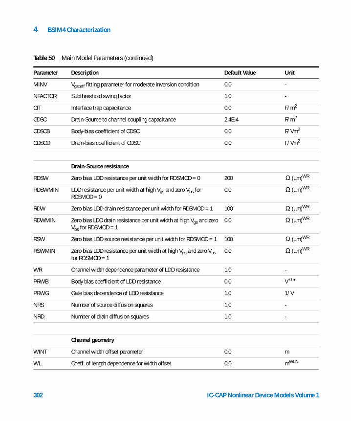
4 BSIM4 Characterization
MINV Vgsteff fitting parameter for moderate inversion condition 0.0 -
NFACTOR Subthreshold swing factor 1.0 -
CIT Interface trap capacitance 0.0 F/m2
CDSC Drain-Source to channel coupling capacitance 2.4E-4 F/m2
CDSCB Body-bias coefficient of CDSC 0.0 F/Vm2
CDSCD Drain-bias coefficient of CDSC 0.0 F/Vm2
Drain-Source resistance
RDSW Zero bias LDD resistance per unit width for RDSMOD = 0 200 (µm)WR
RDSWMIN LDD resistance per unit width at high Vgs and zero Vbs for RDSMOD = 0
0.0 (µm)WR
RDW Zero bias LDD drain resistance per unit width for RDSMOD = 1 100 (µm)WR
RDWMIN Zero bias LDD drain resistance per unit width at high Vgs and zero Vbs for RDSMOD = 1
0.0 (µm)WR
RSW Zero bias LDD source resistance per unit width for RDSMOD = 1 100 (µm)WR
RSWMIN Zero bias LDD resistance per unit width at high Vgs and zero Vbs for RDSMOD = 1
0.0 (µm)WR
WR Channel width dependence parameter of LDD resistance 1.0 -
PRWB Body bias coefficient of LDD resistance 0.0 V-0.5
PRWG Gate bias dependence of LDD resistance 1.0 1/V
NRS Number of source diffusion squares 1.0 -
NRD Number of drain diffusion squares 1.0 -
Channel geometry
WINT Channel width offset parameter 0.0 m
WL Coeff. of length dependence for width offset 0.0 mWLN
Table 50 Main Model Parameters (continued)
Parameter Description Default Value Unit
Ω
Ω
Ω
Ω
Ω
Ω
302 IC-CAP Nonlinear Device Models Volume 1
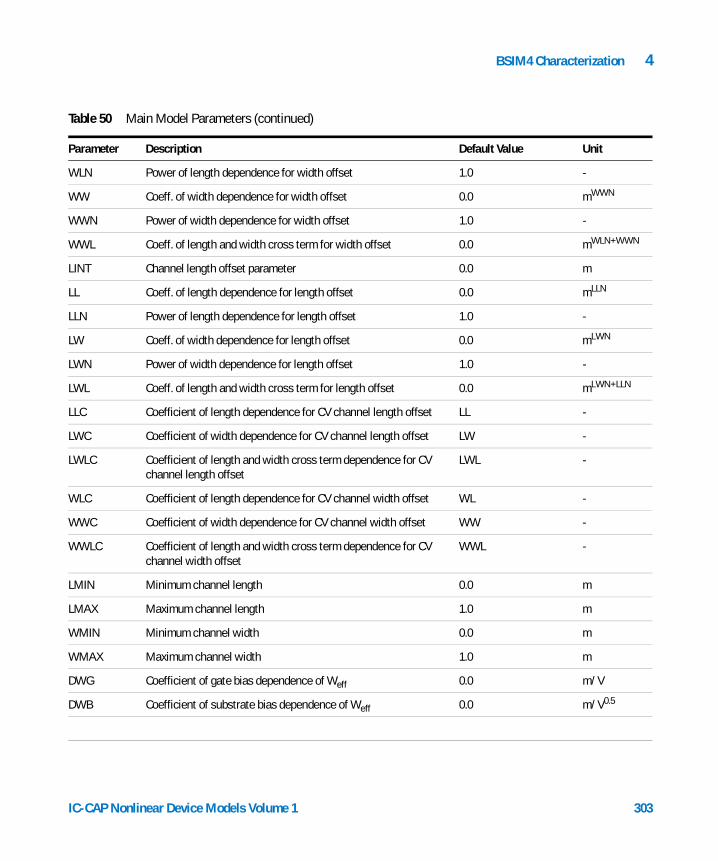
BSIM4 Characterization 4
WLN Power of length dependence for width offset 1.0 -
WW Coeff. of width dependence for width offset 0.0 mWWN
WWN Power of width dependence for width offset 1.0 -
WWL Coeff. of length and width cross term for width offset 0.0 mWLN+WWN
LINT Channel length offset parameter 0.0 m
LL Coeff. of length dependence for length offset 0.0 mLLN
LLN Power of length dependence for length offset 1.0 -
LW Coeff. of width dependence for length offset 0.0 mLWN
LWN Power of width dependence for length offset 1.0 -
LWL Coeff. of length and width cross term for length offset 0.0 mLWN+LLN
LLC Coefficient of length dependence for CV channel length offset LL -
LWC Coefficient of width dependence for CV channel length offset LW -
LWLC Coefficient of length and width cross term dependence for CV channel length offset
LWL -
WLC Coefficient of length dependence for CV channel width offset WL -
WWC Coefficient of width dependence for CV channel width offset WW -
WWLC Coefficient of length and width cross term dependence for CV channel width offset
WWL -
LMIN Minimum channel length 0.0 m
LMAX Maximum channel length 1.0 m
WMIN Minimum channel width 0.0 m
WMAX Maximum channel width 1.0 m
DWG Coefficient of gate bias dependence of Weff 0.0 m/V
DWB Coefficient of substrate bias dependence of Weff 0.0 m/V0.5
Table 50 Main Model Parameters (continued)
Parameter Description Default Value Unit
IC-CAP Nonlinear Device Models Volume 1 303
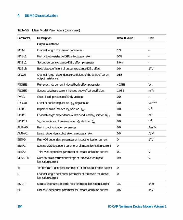
4 BSIM4 Characterization
Output resistance
PCLM Channel length modulation parameter 1.3 -
PDIBL1 First output resistance DIBL effect parameter 0.39 -
PDIBL2 Second output resistance DIBL effect parameter 8.6m -
PDIBLB Body bias coefficient of output resistance DIBL effect 0.0 1/V
DROUT Channel-length dependence coefficient of the DIBL effect on output resistance
0.56 -
PSCBE1 First substrate current induced body-effect parameter 4.24E8 V/m
PSCBE2 Second substrate current induced body-effect coefficient 1.0E-5 m/V
PVAG Gate-bias dependence of Early voltage 0.0 -
FPROUT Effect of pocket implant on Rout degradation 0.0 V/m0.5
PDITS Impact of drain-induced Vth shift on Rout 0.0 V-1
PDITSL Channel-length dependence of drain-induced Vth shift on Rout 0.0 m-1
PDITSD Vds dependence of drain-induced Vth shift on Rout 0.0 V-1
ALPHA0 First impact ionization parameter 0.0 Am/V
ALPHA1 Length dependent substrate current parameter 0.0 A/V
BETA0 First VDS dependent parameter of impact ionization current 0 1/V
BETA1 Second VDS dependent parameter of impact ionization current 0
BETA2 Third VDS dependent parameter of impact ionization current 0.1 V
VDSATII0 Nominal drain saturation voltage at threshold for impact ionization current
0.9 V
TII Temperature dependent parameter for impact ionization current 0
LII Channel length dependent parameter at threshold for impact ionization current
0
ESATII Saturation channel electric field for impact ionization current 1E7 1/m
SII0 First VGS dependent parameter for impact ionization current 0.5 1/V
Table 50 Main Model Parameters (continued)
Parameter Description Default Value Unit
304 IC-CAP Nonlinear Device Models Volume 1

BSIM4 Characterization 4
SII1 Second VGS dependent parameter for impact ionization current 0.1 1/V
SII2 Third VGS dependent parameter for impact ionization current 0
SIID VDS dependent parameter of drain saturation voltage for impact ionization current
0 1/V
Unified Current Saturation
LAMBDA Velocity overshoot coefficientIf not given or , velocity overshoot will be turned off!
2.0E-5 m/s
VTL Thermal velocityIf not given or , source end thermal velocity limit will be turned off!
2.0E-5 m/s
LC Velocity back scattering coefficient(~5E-9m at room temperature)
0.0 m
XN Second velocity back scattering coefficient 3.0
Gate-Induced Drain Leakage model
AGIDL Pre-exponential coefficient for GIDL 0.0 mho(1/Ohm)
BGIDL Exponential coefficient for GIDL 2.3e9 V/m
CGIDL Parameter for body-bias effect on GIDL 0.5 V³
EGIDL Fitting parameter for band bending for GIDL 0.8 V
Gate Dielectric Tunneling Current
AIGBACC Parameter for Igb in accumulation 0.43
BIGBACC Parameter for Igb in accumulation 0.054
CIGBACC Parameter for Igb in accumulation 0.075 1/V
Table 50 Main Model Parameters (continued)
Parameter Description Default Value Unit
0≤
0≤
Fs2( ) g⁄
m-------------------------
Fs2( ) g⁄
m V⋅-------------------------
IC-CAP Nonlinear Device Models Volume 1 305
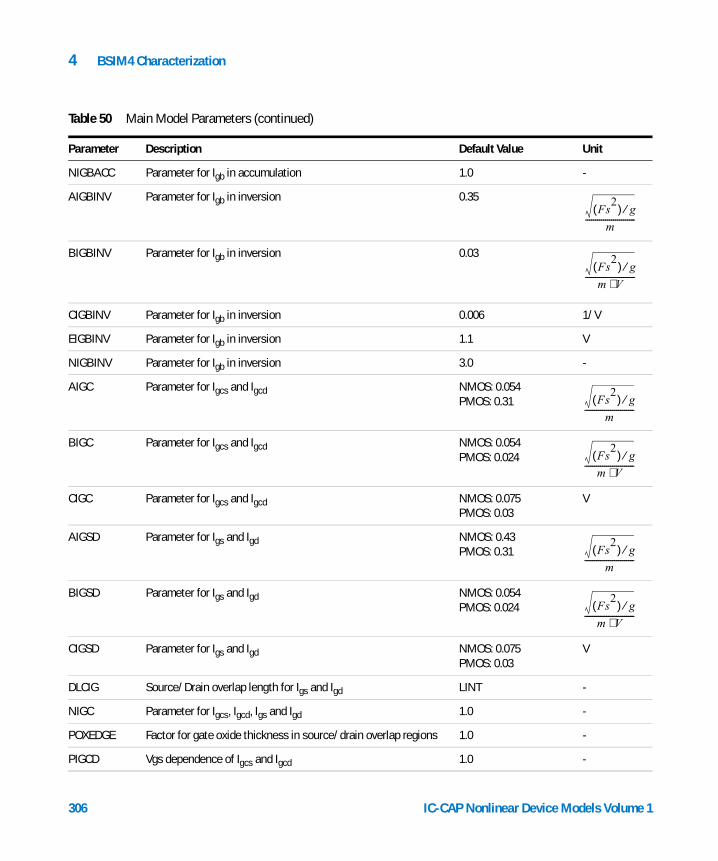
4 BSIM4 Characterization
NIGBACC Parameter for Igb in accumulation 1.0 -
AIGBINV Parameter for Igb in inversion 0.35
BIGBINV Parameter for Igb in inversion 0.03
CIGBINV Parameter for Igb in inversion 0.006 1/V
EIGBINV Parameter for Igb in inversion 1.1 V
NIGBINV Parameter for Igb in inversion 3.0 -
AIGC Parameter for Igcs and Igcd NMOS: 0.054PMOS: 0.31
BIGC Parameter for Igcs and Igcd NMOS: 0.054PMOS: 0.024
CIGC Parameter for Igcs and Igcd NMOS: 0.075PMOS: 0.03
V
AIGSD Parameter for Igs and Igd NMOS: 0.43PMOS: 0.31
BIGSD Parameter for Igs and Igd NMOS: 0.054PMOS: 0.024
CIGSD Parameter for Igs and Igd NMOS: 0.075PMOS: 0.03
V
DLCIG Source/Drain overlap length for Igs and Igd LINT -
NIGC Parameter for Igcs, Igcd, Igs and Igd 1.0 -
POXEDGE Factor for gate oxide thickness in source/drain overlap regions 1.0 -
PIGCD Vgs dependence of Igcs and Igcd 1.0 -
Table 50 Main Model Parameters (continued)
Parameter Description Default Value Unit
Fs2( ) g⁄
m-------------------------
Fs2( ) g⁄
m V⋅-------------------------
Fs2( ) g⁄
m-------------------------
Fs2( ) g⁄
m V⋅-------------------------
Fs2( ) g⁄
m-------------------------
Fs2( ) g⁄
m V⋅-------------------------
306 IC-CAP Nonlinear Device Models Volume 1
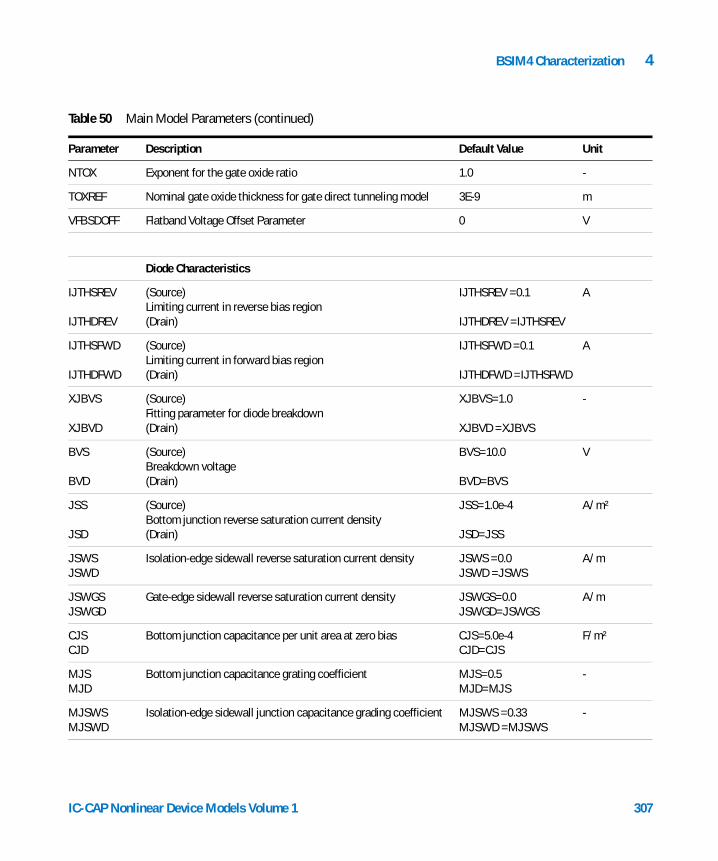
BSIM4 Characterization 4
NTOX Exponent for the gate oxide ratio 1.0 -
TOXREF Nominal gate oxide thickness for gate direct tunneling model 3E-9 m
VFBSDOFF Flatband Voltage Offset Parameter 0 V
Diode Characteristics
IJTHSREV
IJTHDREV
(Source) Limiting current in reverse bias region (Drain)
IJTHSREV =0.1
IJTHDREV =IJTHSREV
A
IJTHSFWD
IJTHDFWD
(Source)Limiting current in forward bias region(Drain)
IJTHSFWD =0.1
IJTHDFWD =IJTHSFWD
A
XJBVS
XJBVD
(Source)Fitting parameter for diode breakdown(Drain)
XJBVS=1.0
XJBVD =XJBVS
-
BVS
BVD
(Source)Breakdown voltage (Drain)
BVS=10.0
BVD=BVS
V
JSS
JSD
(Source)Bottom junction reverse saturation current density(Drain)
JSS=1.0e-4
JSD=JSS
A/m²
JSWSJSWD
Isolation-edge sidewall reverse saturation current density JSWS =0.0JSWD =JSWS
A/m
JSWGS JSWGD
Gate-edge sidewall reverse saturation current density JSWGS=0.0JSWGD=JSWGS
A/m
CJSCJD
Bottom junction capacitance per unit area at zero bias CJS=5.0e-4 CJD=CJS
F/m²
MJS MJD
Bottom junction capacitance grating coefficient MJS=0.5MJD=MJS
-
MJSWSMJSWD
Isolation-edge sidewall junction capacitance grading coefficient MJSWS =0.33MJSWD =MJSWS
-
Table 50 Main Model Parameters (continued)
Parameter Description Default Value Unit
IC-CAP Nonlinear Device Models Volume 1 307

4 BSIM4 Characterization
CJSWS CJSWD
Isolation-edge sidewall junction capacitance per unit area CJSWS= 5.0e-10CJSWD=CJSWS
F/m
CJSWGSCJSWGD
Gate-edge sidewall junction capacitance per unit length CJSWGS =CJSWSCJSWGD =CJSWS
-
MJSWGS MJSWGD
Gate-edge sidewall junction capacitance grading coefficient MJSWGS=MJSWSMJSWGD=MJSWS
-
PBS Source bottom junction built-in potential PBS=1.0 V
PBD Drain bottom junction built-in potential PBD=PBS V
PBSWS Isolation-edge sidewall junction built-in potential of source junction
PBSWS =1.0 V
PBSWD Isolation-edge sidewall junction built-in potential of drain junction
PBSWD=PBSWS V
PBSWGS Gate-edge sidewall junction built-in potential of source junction PBSWGS =PBSWS V
PBSWGD Gate-edge sidewall junction built-in potential of drain junction PBSWGD=PBSWS V
Asymmetric Source/Drain Junction Diode Model
JTSSJTSD
Bottom trap-assisted saturation current density(Source side / Drain side)
0.0=JTSS
A/m
JTSSWSJTSSWD
STI sidewall trap-assisted saturation current density(Source side / Drain side)
0.0JTSSWS
A/m
JTSSWGSJTSSWGD
Gate sidewall trap-assisted saturation current density(Source side / Drain side)
0.0JTSSWGS
A/m
NJTS Non-ideality factor for JTSS, JTSD 20
NJTSSW Non-ideality factor for JTSSWS, JTSSWD 20
NJTSSWG Non-ideality factor for JTSSWGS, JTSSWGD 20
XTSSXTSD
Power dependence of JTSS, JTSD on temperature(Source side / Drain side)
0.02
XTSSWSXTSSWD
Power dependence of JTSSWS, JTSSWD on temperature(Source side / Drain side)
0.02
Table 50 Main Model Parameters (continued)
Parameter Description Default Value Unit
308 IC-CAP Nonlinear Device Models Volume 1
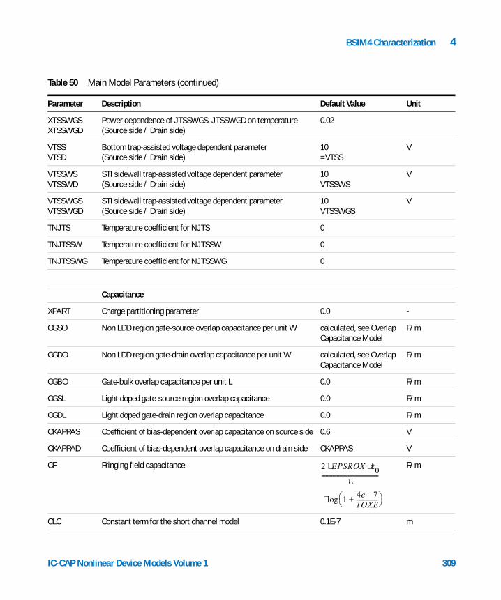
BSIM4 Characterization 4
XTSSWGSXTSSWGD
Power dependence of JTSSWGS, JTSSWGD on temperature(Source side / Drain side)
0.02
VTSSVTSD
Bottom trap-assisted voltage dependent parameter(Source side / Drain side)
10=VTSS
V
VTSSWSVTSSWD
STI sidewall trap-assisted voltage dependent parameter(Source side / Drain side)
10VTSSWS
V
VTSSWGSVTSSWGD
STI sidewall trap-assisted voltage dependent parameter(Source side / Drain side)
10VTSSWGS
V
TNJTS Temperature coefficient for NJTS 0
TNJTSSW Temperature coefficient for NJTSSW 0
TNJTSSWG Temperature coefficient for NJTSSWG 0
Capacitance
XPART Charge partitioning parameter 0.0 -
CGSO Non LDD region gate-source overlap capacitance per unit W calculated, see Overlap Capacitance Model
F/m
CGDO Non LDD region gate-drain overlap capacitance per unit W calculated, see Overlap Capacitance Model
F/m
CGBO Gate-bulk overlap capacitance per unit L 0.0 F/m
CGSL Light doped gate-source region overlap capacitance 0.0 F/m
CGDL Light doped gate-drain region overlap capacitance 0.0 F/m
CKAPPAS Coefficient of bias-dependent overlap capacitance on source side 0.6 V
CKAPPAD Coefficient of bias-dependent overlap capacitance on drain side CKAPPAS V
CF Fringing field capacitance F/m
CLC Constant term for the short channel model 0.1E-7 m
Table 50 Main Model Parameters (continued)
Parameter Description Default Value Unit
2 EPSROX ε0⋅ ⋅
π-----------------------------------------
14e 7–TOXE----------------+
log⋅
IC-CAP Nonlinear Device Models Volume 1 309
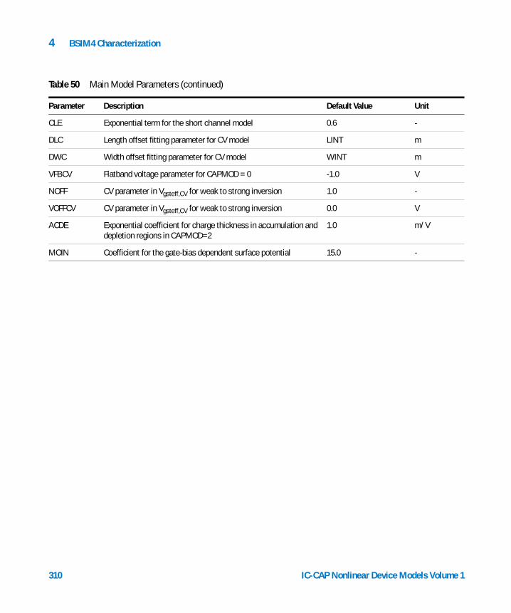
4 BSIM4 Characterization
CLE Exponential term for the short channel model 0.6 -
DLC Length offset fitting parameter for CV model LINT m
DWC Width offset fitting parameter for CV model WINT m
VFBCV Flatband voltage parameter for CAPMOD = 0 -1.0 V
NOFF CV parameter in Vgsteff,CV for weak to strong inversion 1.0 -
VOFFCV CV parameter in Vgsteff,CV for weak to strong inversion 0.0 V
ACDE Exponential coefficient for charge thickness in accumulation and depletion regions in CAPMOD=2
1.0 m/V
MOIN Coefficient for the gate-bias dependent surface potential 15.0 -
Table 50 Main Model Parameters (continued)
Parameter Description Default Value Unit
310 IC-CAP Nonlinear Device Models Volume 1
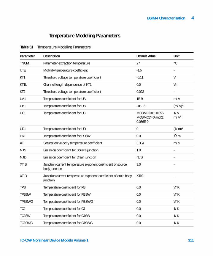
BSIM4 Characterization 4
Temperature Modeling Parameters
Table 51 Temperature Modeling Parameters
Parameter Description Default Value Unit
TNOM Parameter extraction temperature 27 °C
UTE Mobility temperature coefficient -1.5 -
KT1 Threshold voltage temperature coefficient -0.11 V
KT1L Channel length dependence of KT1 0.0 Vm
KT2 Threshold voltage temperature coefficient 0.022 -
UA1 Temperature coefficient for UA 1E-9 m/V
UB1 Temperature coefficient for UB -1E-18 (m/V)2
UC1 Temperature coefficient for UC MOBMOD=1: 0.056MOBMOD=0 and 2: 0.056E-9
1/Vm/V2
UD1 Temperature coefficient for UD 0 (1/m)²
PRT Temperature coefficient for RDSW 0.0 m
AT Saturation velocity temperature coefficient 3.3E4 m/s
NJS Emission coefficient for Source junction 1.0 -
NJD Emission coefficient for Drain junction NJS -
XTIS Junction current temperature exponent coefficient of source body junction
3.0 -
XTID Junction current temperature exponent coefficient of drain body junction
XTIS -
TPB Temperature coefficient for PB 0.0 V/K
TPBSW Temperature coefficient for PBSW 0.0 V/K
TPBSWG Temperature coefficient for PBSWG 0.0 V/K
TCJ Temperature coefficient for CJ 0.0 1/K
TCJSW Temperature coefficient for CJSW 0.0 1/K
TCJSWG Temperature coefficient for CJSWG 0.0 1/K
Ω
IC-CAP Nonlinear Device Models Volume 1 311
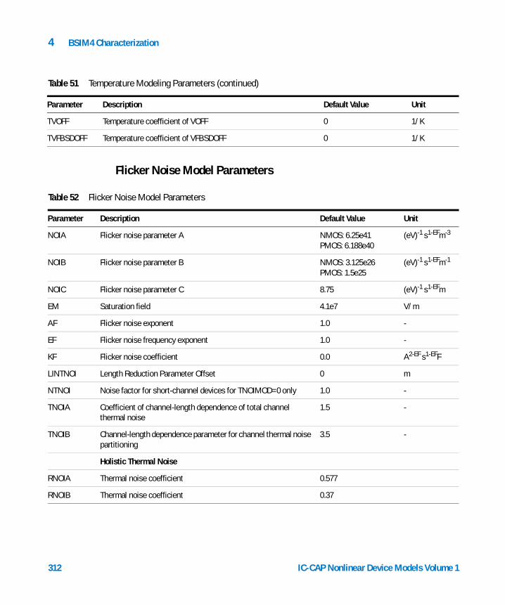
4 BSIM4 Characterization
Flicker Noise Model Parameters
TVOFF Temperature coefficient of VOFF 0 1/K
TVFBSDOFF Temperature coefficient of VFBSDOFF 0 1/K
Table 52 Flicker Noise Model Parameters
Parameter Description Default Value Unit
NOIA Flicker noise parameter A NMOS: 6.25e41
PMOS: 6.188e40(eV)-1 s1-EFm-3
NOIB Flicker noise parameter B NMOS: 3.125e26PMOS: 1.5e25
(eV)-1 s1-EFm-1
NOIC Flicker noise parameter C 8.75 (eV)-1 s1-EFm
EM Saturation field 4.1e7 V/m
AF Flicker noise exponent 1.0 -
EF Flicker noise frequency exponent 1.0 -
KF Flicker noise coefficient 0.0 A2-EF s1-EFF
LINTNOI Length Reduction Parameter Offset 0 m
NTNOI Noise factor for short-channel devices for TNOIMOD=0 only 1.0 -
TNOIA Coefficient of channel-length dependence of total channel thermal noise
1.5 -
TNOIB Channel-length dependence parameter for channel thermal noise partitioning
3.5 -
Holistic Thermal Noise
RNOIA Thermal noise coefficient 0.577
RNOIB Thermal noise coefficient 0.37
Table 51 Temperature Modeling Parameters (continued)
Parameter Description Default Value Unit
312 IC-CAP Nonlinear Device Models Volume 1
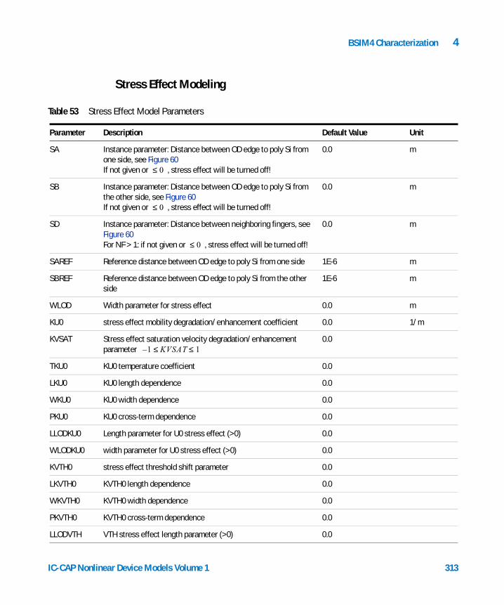
BSIM4 Characterization 4
Stress Effect Modeling
Table 53 Stress Effect Model Parameters
Parameter Description Default Value Unit
SA Instance parameter: Distance between OD edge to poly Si from one side, see Figure 60If not given or , stress effect will be turned off!
0.0 m
SB Instance parameter: Distance between OD edge to poly Si from the other side, see Figure 60If not given or , stress effect will be turned off!
0.0 m
SD Instance parameter: Distance between neighboring fingers, see Figure 60For NF > 1: if not given or , stress effect will be turned off!
0.0 m
SAREF Reference distance between OD edge to poly Si from one side 1E-6 m
SBREF Reference distance between OD edge to poly Si from the other side
1E-6 m
WLOD Width parameter for stress effect 0.0 m
KU0 stress effect mobility degradation/enhancement coefficient 0.0 1/m
KVSAT Stress effect saturation velocity degradation/enhancement parameter
0.0
TKU0 KU0 temperature coefficient 0.0
LKU0 KU0 length dependence 0.0
WKU0 KU0 width dependence 0.0
PKU0 KU0 cross-term dependence 0.0
LLODKU0 Length parameter for U0 stress effect (>0) 0.0
WLODKU0 width parameter for U0 stress effect (>0) 0.0
KVTH0 stress effect threshold shift parameter 0.0
LKVTH0 KVTH0 length dependence 0.0
WKVTH0 KVTH0 width dependence 0.0
PKVTH0 KVTH0 cross-term dependence 0.0
LLODVTH VTH stress effect length parameter (>0) 0.0
0≤
0≤
0≤
1 KVSAT 1≤≤–
IC-CAP Nonlinear Device Models Volume 1 313
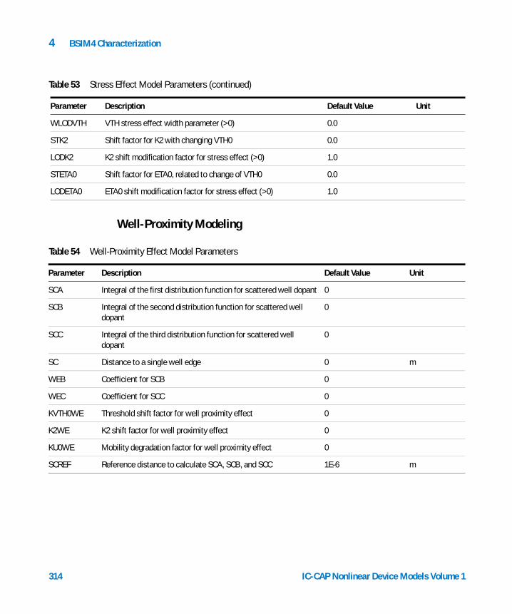
4 BSIM4 Characterization
Well-Proximity Modeling
WLODVTH VTH stress effect width parameter (>0) 0.0
STK2 Shift factor for K2 with changing VTH0 0.0
LODK2 K2 shift modification factor for stress effect (>0) 1.0
STETA0 Shift factor for ETA0, related to change of VTH0 0.0
LODETA0 ETA0 shift modification factor for stress effect (>0) 1.0
Table 54 Well-Proximity Effect Model Parameters
Parameter Description Default Value Unit
SCA Integral of the first distribution function for scattered well dopant 0
SCB Integral of the second distribution function for scattered well dopant
0
SCC Integral of the third distribution function for scattered well dopant
0
SC Distance to a single well edge 0 m
WEB Coefficient for SCB 0
WEC Coefficient for SCC 0
KVTH0WE Threshold shift factor for well proximity effect 0
K2WE K2 shift factor for well proximity effect 0
KU0WE Mobility degradation factor for well proximity effect 0
SCREF Reference distance to calculate SCA, SCB, and SCC 1E-6 m
Table 53 Stress Effect Model Parameters (continued)
Parameter Description Default Value Unit
314 IC-CAP Nonlinear Device Models Volume 1
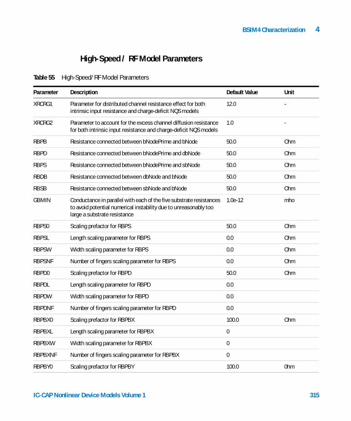
BSIM4 Characterization 4
High-Speed / RF Model Parameters
Table 55 High-Speed/RF Model Parameters
Parameter Description Default Value Unit
XRCRG1 Parameter for distributed channel resistance effect for both intrinsic input resistance and charge-deficit NQS models
12.0 -
XRCRG2 Parameter to account for the excess channel diffusion resistance for both intrinsic input resistance and charge-deficit NQS models
1.0 -
RBPB Resistance connected between bNodePrime and bNode 50.0 Ohm
RBPD Resistance connected between bNodePrime and dbNode 50.0 Ohm
RBPS Resistance connected between bNodePrime and sbNode 50.0 Ohm
RBDB Resistance connected between dbNode and bNode 50.0 Ohm
RBSB Resistance connected between sbNode and bNode 50.0 Ohm
GBMIN Conductance in parallel with each of the five substrate resistances to avoid potential numerical instability due to unreasonably too large a substrate resistance
1.0e-12 mho
RBPS0 Scaling prefactor for RBPS 50.0 Ohm
RBPSL Length scaling parameter for RBPS 0.0 Ohm
RBPSW Width scaling parameter for RBPS 0.0 Ohm
RBPSNF Number of fingers scaling parameter for RBPS 0.0 Ohm
RBPD0 Scaling prefactor for RBPD 50.0 Ohm
RBPDL Length scaling parameter for RBPD 0.0
RBPDW Width scaling parameter for RBPD 0.0
RBPDNF Number of fingers scaling parameter for RBPD 0.0
RBPBX0 Scaling prefactor for RBPBX 100.0 Ohm
RBPBXL Length scaling parameter for RBPBX 0
RBPBXW Width scaling parameter for RBPBX 0
RBPBXNF Number of fingers scaling parameter for RBPBX 0
RBPBY0 Scaling prefactor for RBPBY 100.0 0hm
IC-CAP Nonlinear Device Models Volume 1 315
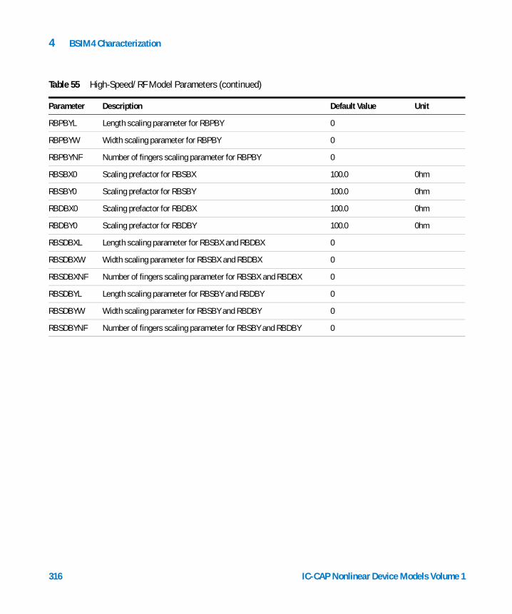
4 BSIM4 Characterization
RBPBYL Length scaling parameter for RBPBY 0
RBPBYW Width scaling parameter for RBPBY 0
RBPBYNF Number of fingers scaling parameter for RBPBY 0
RBSBX0 Scaling prefactor for RBSBX 100.0 0hm
RBSBY0 Scaling prefactor for RBSBY 100.0 0hm
RBDBX0 Scaling prefactor for RBDBX 100.0 0hm
RBDBY0 Scaling prefactor for RBDBY 100.0 0hm
RBSDBXL Length scaling parameter for RBSBX and RBDBX 0
RBSDBXW Width scaling parameter for RBSBX and RBDBX 0
RBSDBXNF Number of fingers scaling parameter for RBSBX and RBDBX 0
RBSDBYL Length scaling parameter for RBSBY and RBDBY 0
RBSDBYW Width scaling parameter for RBSBY and RBDBY 0
RBSDBYNF Number of fingers scaling parameter for RBSBY and RBDBY 0
Table 55 High-Speed/RF Model Parameters (continued)
Parameter Description Default Value Unit
316 IC-CAP Nonlinear Device Models Volume 1
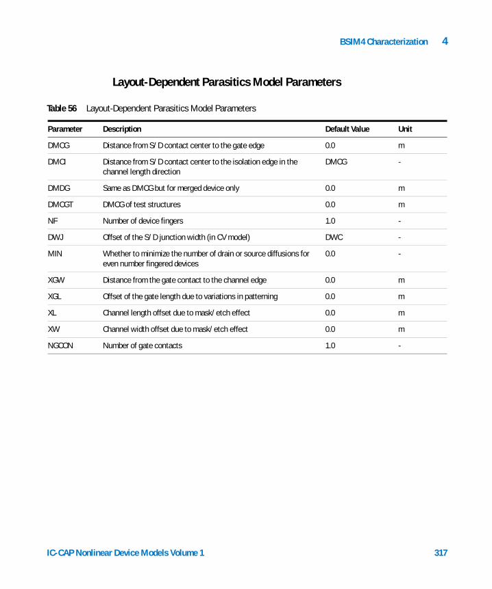
BSIM4 Characterization 4
Layout-Dependent Parasitics Model Parameters
Table 56 Layout-Dependent Parasitics Model Parameters
Parameter Description Default Value Unit
DMCG Distance from S/D contact center to the gate edge 0.0 m
DMCI Distance from S/D contact center to the isolation edge in the channel length direction
DMCG -
DMDG Same as DMCG but for merged device only 0.0 m
DMCGT DMCG of test structures 0.0 m
NF Number of device fingers 1.0 -
DWJ Offset of the S/D junction width (in CV model) DWC -
MIN Whether to minimize the number of drain or source diffusions for even number fingered devices
0.0 -
XGW Distance from the gate contact to the channel edge 0.0 m
XGL Offset of the gate length due to variations in patterning 0.0 m
XL Channel length offset due to mask/etch effect 0.0 m
XW Channel width offset due to mask/etch effect 0.0 m
NGCON Number of gate contacts 1.0 -
IC-CAP Nonlinear Device Models Volume 1 317
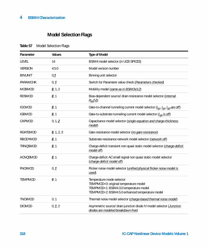
4 BSIM4 Characterization
Model Selection Flags
Table 57 Model Selection Flags
Parameter Values Type of Model
LEVEL 14 BSIM4 model selector (in UCB SPICE3)
VERSION 4.5.0 Model version number
BINUNIT 0,1 Binning unit selector
PARAMCHK 0, 1 Switch for Parameter value check (Parameters checked)
MOBMOD 0, 1, 2 Mobility model (same as in BSIM3v3.2)
RDSMOD 0, 1 Bias-dependent source/drain resistance model selector (internal Rds(V))
IGCMOD 0, 1 Gate-to-channel tunneling current model selector (Igc, Igs, Igd are off)
IGBMOD 0, 1 Gate-to-substrate tunneling current model selector (Igb is off)
CAPMOD 0, 1, 2 Capacitance model selector (single-equation and charge-thickness model)
RGATEMOD 0, 1, 2, 3 Gate resistance model selector (no gate resistance)
RBODYMOD 0, 1 Substrate resistance network model selector (network off)
TRNQSMOD 0, 1 Charge-deficit transient non quasi static model selector (charge-deficit model off)
ACNQSMOD 0, 1 Charge-deficit AC small signal non quasi static model selector (charge-deficit model off)
FNOIMOD 0, 1 Flicker noise model selector (unified physical flicker noise model is used)
TEMPMOD 0, 1 Temperature mode selectorTEMPMOD=0: original temperature modelTEMPMOD=1: BSIM4.3.0 temperature modelTEMPMOD=2: BSIM4.5.0 enhanced temperature model
TNOIMOD 0, 1 Thermal noise model selector (charge-based thermal noise model)
DIOMOD 0, 1, 2 Asymmetric source/drain junction diode IV model selector (Junction diodes are modeled breakdown-free)
318 IC-CAP Nonlinear Device Models Volume 1
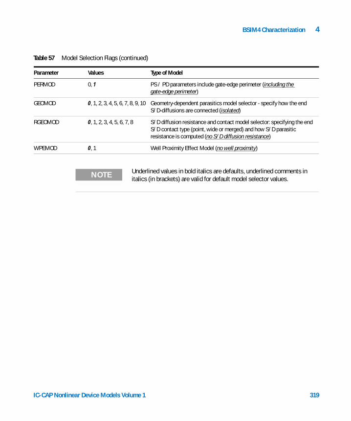
BSIM4 Characterization 4
PERMOD 0, 1 PS / PD parameters include gate-edge perimeter (including the gate-edge perimeter)
GEOMOD 0, 1, 2, 3, 4, 5, 6, 7, 8, 9, 10 Geometry-dependent parasitics model selector - specify how the end S/D-diffusions are connected (isolated)
RGEOMOD 0, 1, 2, 3, 4, 5, 6, 7, 8 S/D diffusion resistance and contact model selector: specifying the end S/D contact type (point, wide or merged) and how S/D parasitic resistance is computed (no S/D diffusion resistance)
WPEMOD 0, 1 Well Proximity Effect Model (no well proximity)
NOTE Underlined values in bold italics are defaults, underlined comments in italics (in brackets) are valid for default model selector values.
Table 57 Model Selection Flags (continued)
Parameter Values Type of Model
IC-CAP Nonlinear Device Models Volume 1 319
4 BSIM4 Characterization
References
320
1 BSIM4.5.0 Manual, University of California at Berkeley, Copyright © 2004 The Regents of the University of California. See the web site of the device research group at UCB. You can download the manual from the Internet, using the following Web address:http://www-device.eecs.berkeley.edu/~bsim3/bsim4_get.htmll
2 “Characterization System for Submicron CMOS Technologies,” JESSI Reports AC41 94-1 through 94-6
3 C. Enz, “MOS Transistor Modeling for RF IC Design”, Silicon RF IC: Modeling and Simulation Workshop, Lausanne 2000
4 T. Gneiting, “BSIM4, BSIM3v3 and BSIMSOI RF MOS Modeling”, RF Modeling and Measurement Workshop, European Microwave Week, Paris 2000
5 William Liu, “Mosfet Models for Spice Simulation: Including BSIM3v3 and BSIM4”, John Wiley & Sons, January 2001
6 M. J. Deen (Ed.), T.A.Fjeldly, “CMOS RF Modeling, Characterization and Applications”, Worldscientific, Co-authors: F.Sischka and T.Gneiting
7 X. Xi, M. Dunga, A. M. Niknejad, C. Hu, “Description of BSIM450 Model Enhancements”, June 24, 2005, to be found at the following Web address: http://www-device.eecs.berkeley.edu/~bsim3/BSIM4/BSIM450/doc/BSIM450_Enhancement.pdf
Acknowledgements
The BSIM4 model was developed by the UC Berkeley BSIM Device Research Group of the Department of Electrical Engineering and Computer Science, University of California, Berkeley and is copyrighted by the University of California.
IC-CAP Nonlinear Device Models Volume 1
Agilent 85190A IC-CAP 2008Nonlinear Device Models Volume 1
5BSIM3v3 Characterization
The BSIM3 Model 327
The Unified I-V Model of BSIM3v3 330
Capacitance Model 368
High Frequency Behavior 385
Temperature Dependence 401
Noise Model 409
SPICE Model Parameters 412
Test structures for Deep Submicron CMOS Processes 422
Extraction of Model Parameters 445
Binning of Model Parameters 452
Importing older version BSIM3v3 Files 462
References 466
This Chapter explains the theoretical background of the BSIM3 model. Using the Modeling Package is described in Chapter 1, “Using the MOS Modeling Packages”. This version is based on the BSIM3v3.3.0 model, released by the University of California at Berkeley in July 2005.
What’s new inside the BSIM3 Modeling Package:
This section lists the enhancements and changes made to the Modeling Package for each revision since IC-CAP 2002. They are listed in reverse order so that the new version is on top, followed by changes made in former versions.
321Agilent Technologies

322
5 BSIM3v3 Characterization
New features in the BSIM3 Modeling Package, Rev. IC-CAP 2006, spring 2007
The BSIM3 model version has been enhanced to the model version BSIM3v3.3.0.
The GUI has been updated to the same look as the BSIM4 and PSP Modeling Packages.
New features in the BSIM3 Modeling Package, Rev. IC-CAP 2004, spring 2005
1.) BSIM3_DC_CV_Measure
The time to load a new project has been dramatically reduced (also in BSIM3_DC_CV_Extract, BSIM3_RF_Measure, BSIM3_RF_Extract).
List sweeps are now supported.
2.) BSIM3_DC_CV_Extract
The extraction flow has been enhanced to store and retrieve complete extraction scenarios including intermediate results and boundary settings.
The usability of the plot optimizer inside the BSIM3 Package has been enhanced and user configured plot optimizers can be easily integrated into the extraction flow.
3.) BSIM3_RF_Measure
New scheme to define de-embedding structures.
New features in the BSIM3 Modeling Package, Rev. IC-CAP 2004, January 2004
1.) General
The Graphic User Interface from BSIM4 has been adopted. One of the main advantages of this concept is that the measured data can be used by BSIM3 and BSIM4 Modeling Packages for parameter extraction!!!
IC-CAP Nonlinear Device Models Volume 1

BSIM3v3 Characterization 5
IC-CAP Nonlinear Device Models Vo
The BSIM3 Modeling Package can now generate model cards and scalable RF models for the following simulators:
Spice3 (delivered with IC-CAP)
Advanced Design System
Hspice
Spectre
The documentation was totally reworked to account for the common user interface with the BSIM4 Modeling Package and similar upcoming modeling products.
In addition, a detailed description of all the files of the Modeling Package is given. All temperatures in the setup and documentation are now given in [K] instead of [degree C].
Currently, the supported model is BSIM3v3.2.4, released on Dec.21st, 2001.
2.) BSIM3_DC_CV_Measure
The Keithley switching matrix models K707 and K708a are now supported.
The maximum compliance values can now be defined together with the other measurement settings.
Three new functions are implemented to drive the BSIM3_DC_CV_Measure module from a wafer prober control macro. An example for such a control macro can be found in .../examples/model_files/mosfet/BSIM3/examples/waferprober/prober_control.mdl
3.) BSIM3_DC_CV_Extract
A complete new extraction flow is implemented. A certain extraction group (e.g., 'Basic VTH, Mobility') can be invoked several times with different configurations.
Moreover, the flow inside an extraction group can be specified in any desired order.
lume 1 323
324
5 BSIM3v3 Characterization
This gives the highest available flexibility for adopting any parameter extraction to a certain process.
Automatic generation of binned model files is now supported. A new folder Binning in the BSIM3_DC_CV_Extract module allows the specification of the binning areas as well as extended binning. Final circuits are generated for Hspice, Spectre, and ADS.
Generation of HTML files has been enhanced to include a navigation tree through all results. In addition, all measured data at each temperature for each device is compared with the simulated results.
The new IC-CAP feature Plot Optimizer is supported by a user friendly configuration of the devices and setups for a final fine tuning approach.
A new function is implemented to extract multiple projects in batch mode. This can be very useful for statistical modeling, where a large number of model parameter sets must be generated for the same type of devices but from different measured test chips. Please see the macro 'Example_Wafer_Extraction' in the BSIM3_DC_CV_Extract.mdl file.
Parameter extractions have been steadily enhanced due to user's feedback.
4.) BSIM3_RF_Measure
No changes made.
5) BSIM3_RF_Extract
A complete new extraction flow is implemented. Please see 3.) BSIM3_DC_CV_Extract for more details.
The automatic generation of HTML files has been enhanced to include a navigation tree through all results.
IC-CAP Nonlinear Device Models Volume 1
BSIM3v3 Characterization 5
IC-CAP Nonlinear Device Models Vo
6) Documentation
The documentation was totally reworked to account for the common user interface with the BSIM4 Modeling Package and similar upcoming modeling products.
In addition, a detailed description of all files of the Modeling Packages is included.
New features in the BSIM3 Modeling Package, Rev. IC-CAP 2002, March 2003
1.) General
This is an update to the already existing BSIM3v3 Modeling Package in IC-CAP.
The complete user interface and data structure was modified and reworked to have the same style as the existing BSIM4 Modeling Package.
One of the main advantages of this concept is the usage of measured data by the BSIM3 Modeling Package as well as the BSIM4 Modeling Package for parameter extraction
Please note, for compatibility reasons the old BSIM3v3 files can still be accessed in the $ICCAP_ROOT/examples/model_files/mosfet/bsim3v3 directory.
The new style files are located in the directory:$ICCAP_ROOT/examples/model_files/mosfet/bsim3
Don't get confused by the missing version information of the "bsim3" term. The new style files don’t use the version information any more.
2.) BSIM3_DC_CV_Measure
A feature "Import BSIM3v3" was added to reuse data in the file format of the former BSIM3v3 Modeling Package.
The measured data of the new BSIM3 Modeling Package is now in a format that can be used for the generation of BSIM3 and BSIM4 models
lume 1 325

326
5 BSIM3v3 Characterization
3.) BSIM3_DC_CV_Extract
The existing extraction functions have been ported to the new style user interface.
A new, more user friendly HTML report can be generated, which allows a comparison of measured and simulated data for each device. In addition, the report can be easily included in a word processing program.
4.) BSIM3_RF_Measure
This module measures all data which is necessary for the generation of RF models. The data is compatible with the BSIM4_RF_Measure module and can also be used for the generation of BSIM4 RF models.
5) BSIM3_RF_Extract
A new, fully scalable subcircuit model for the BSIM3 RF behavior was added. The user can now select whether he wants to create a single device model (one model for each test device) or a fully scalable model that covers all available test devices.
6) BSIM3_Tutorial
These are the well known files for learning more about the BSIM3 model itself.
7) Documentation
The Help buttons are still linked to the BSIM4 Online Help. This is OK, because the usage of the BSIM3 Modeling Package and the BSIM4 Modeling Package is identical.
For more information about the BSIM3 model itself, please refer to this chapter.
A reworked version of the documentation will be included in the IC-CAP 2004 release.
IC-CAP Nonlinear Device Models Volume 1
BSIM3v3 Characterization 5
The BSIM3 Model
IC-CAP Nonlinear Device Models Vo
The BSIM3 model (BSIM = Berkeley Short channel Insulated gate field effect transistor Model) was published by the University of California at Berkeley in July 1993. BSIM3 is a public model and is intended to simulate analog and digital circuits that consist of deep submicron MOS devices down to channel lengths of 0.18 micron. Since this channel length is no longer state-of-the-art for modern MOS devices, the model has been adopted several times to model effects not present in devices with greater channel lengths.
BSIM3 is a physical model with built-in dependencies of important device dimensions and process parameters like the channel length and width, the gate oxide thickness, substrate doping concentration and LDD structures. Due to its physical nature and its built-in geometry dependence, the prediction of device behavior of advanced devices based on the parameters of the existing process is possible. As a further improvement, one set of model parameters covers the whole range of channel lengths and channel widths of a certain process that can be used in circuit designs. Due to the physical meaning of many model parameters, the BSIM3 model is the ideal basis for the statistical analysis of process fluctuations.
BSIM3 can model the following physical effects of modern submicron MOS transistors:
• Threshold Voltage
• Vertical and lateral non-uniform doping
• Short channel effects
• Narrow channel effects
• Mobility
• Mobility reduction due to vertical fields
• Carrier Velocity Saturation
• Drain Current
lume 1 327
328
5 BSIM3v3 Characterization
• Bulk charge effect
• Subthreshold conduction
• Source/drain parasitic resistance
• Bulk Current
• Output Resistance
• Drain induced barrier lowering (DIBL)
• Channel length modulation (CLM)
• Substrate current induced body effect (SCBE)
• Short channel capacitance model
• Temperature dependence of the device behavior
For a detailed description of these features, refer to the BSIM3 manual from Berkeley University. You can order this manual from Berkeley or you can get it over the Internet. See “References” on page 466 for details.
The BSIM3v3 Modeling Package provides a complete extraction strategy for the model parameters of the BSIM3v3.3.0 model. The extraction routines are based on the BSIM3v3.3.0 device equations to ensure that the extracted model parameters represent as good as possible the original physical meaning. Therefore, no or only a minimum of optimization is needed to get a good fit between measured and simulated device behavior.
The routines of this release refer to version 3.3.0 of the BSIM3 model that was released by University of California at Berkeley in July 2005.
Versions of the BSIM3 Model
University of California at Berkeley released four versions of its BSIM3 model. The first three versions have differences in some model parameters, and the model parameter sets are not compatible.
The following example of the parameter UC, which is a part of the mobility reduction, demonstrates the problem:
In BSIM3v2, the effective mobility µeff was calculated according to the following formula:
IC-CAP Nonlinear Device Models Volume 1

BSIM3v3 Characterization 5
IC-CAP Nonlinear Device Models Vo
In BSIM3v3.2.2, the formula changed to:
It can easily be recognized, that UC has quite different values in both equations.
That means, if BSIM3v2 is implemented in the simulator and the parameter is extracted for BSIM3v3.2.2, the simulation will give catastrophic results (in the case of UC).
Therefore, you must be sure that you use the same version of BSIM3 in both your simulator and your extraction tool.
The latest release, BSIM3v3.3.0 is a minor change to BSIM3v3.2.4 with only a few bug fixes and some enhancements in noise modeling. The model equations used are mainly the same in those versions.
Additionally, a few effects are modeled by introducing the ACNQSMOD as well as the LINTNOI model parameters from BSIM4.
µeff
µo
1 Ua Vgs Vth+( ) Tox⁄( ) Ub Vgs Vth+( ) Tox⁄( )2 UcVbs+ + +----------------------------------------------------------------------------------------------------------------------------------------------------------=
µeff
µo
1 Ua Uc+ Vbseff( ) Vgsteff 2Vth+( ) Tox⁄( ) Ub Vgsteff 2Vth+( ) Tox⁄( )2+ +----------------------------------------------------------------------------------------------------------------------------------------------------------------------------------------------------=
lume 1 329
5 BSIM3v3 Characterization
The Unified I-V Model of BSIM3v3
330
For a complete summary of all equations of the BSIM3v3.2.4 model, please refer to the original documentation from University of California at Berkeley (see “References” on page 466 to order this paper). The main equations of the BSIM3v3.3.0 model are shown together with a graphical representation for a better understanding of the model.
Please use the models BSIM3_DC_Tutorial.mdl, BSIM3_CV_Tutorial.mdl, BSIM3_AC_Noise_Tutorial.mdl, or BSIM3_Temp_Tutorial.mdl provided with the BSIM3 Modeling Package to visualize most of the model parameters influences onto the device diagrams. Load the file into IC-CAP to see how certain parameters affect the behavior of a deep submicron MOS transistor.
Threshold Voltage
The threshold voltage is one of the most important parameters of deep submicron MOS transistors and is affected by many different effects when the devices are scaled down into the region of 0.1 microns. The complete equation of the threshold voltage in BSIM3v3.3.0 is given below.
(45)
The different parts of this complex equation are expressed by the following sub-equations in more detail:
Vth VTideal ∆Vth 1( ) ∆Vth 2( ) ∆Vth 3( )– ∆Vth 4( )– ∆Vth 5( ) ∆Vth 6( )–+ + +=
IC-CAP Nonlinear Device Models Volume 1
BSIM3v3 Characterization 5
IC-CAP Nonlinear Device Models Vo
(46)
Ideal Threshold Voltage
The basic equation of the threshold voltage is:
(47)
(48)
(49)
where:
Vth Vth0 K1 Φs–=
+K1
ToxToxm-------------- Φs Vbseff– K2
ToxToxm--------------Vbseff
–
+K1
ToxToxm-------------- 1
NlxLeff----------+
1–
Φs
DVT0 e
DVT1 Leff2 lt
----------–
2e
DVT1
Lefflt
----------–
+ Vbi Φs–( )–
DVT0w e
DVT1w
WeffLeff2 ltw
-----------------------–
2e
DVT1w
WeffLeffltw
-----------------------–
+ Vbi Φ–(–
+ K3 K3bVbseff+( )Tox
Weff W0+( )-------------------------------Φs
e
Dsub
Leff2lt0----------–
2e
Dsub
Lefflt0
----------–
+– Eta0 EtabVbseff+( )Vds
VTideal Vth0 VFB Φs K1 Φs+ += =
Φs 2Vtm0 lnNchni0----------
at T Tnom==
Vtm0
kBTnomq
---------------------=
lume 1 331

332
5 BSIM3v3 Characterization
This equation had been implemented into the first MOS simulation models assuming long and wide channels and uniform substrate doping. The following sections describe the effects that overlay this basic equation.
Non-Uniform Vertical Channel Doping
The substrate doping concentration N is not constant in the vertical direction of the channel, as shown in the following figure.
It is usually higher near the silicon to silicon dioxide interface than deeper in the substrate. This higher doping concentration is used to adjust the threshold voltage of the device. The distribution of impurity atoms inside the substrate is approximately a half Gaussian distribution, which can be approximated by a step function with NCH for the peak concentration in the channel near the Si-SiO2 interface and Nsub in the deep bulk. XT is the depth where the approximation of the implant profile switches from NCH to NSUB. The non-uniform vertical channel doping affects the threshold
Vthideal = ideal threshold voltage
VFB = flatband voltage
Φs = surface potential
ni = 1.45 • 1010 (Tnom/300.15)1.5 (21.5566 - Eg0/2Vtmo)
Eg0 = 1.16 - 7.02 • 10-4 Tnom2/(Tnom + 1108)
Figure 70 Vertical Doping Profile in the Channel
IC-CAP Nonlinear Device Models Volume 1

BSIM3v3 Characterization 5
IC-CAP Nonlinear Device Models Vo
voltage when a bulk source voltage is applied to the device and is represented here as the part ∆Vth(1) of the overall threshold voltage.
(50)
(51)
(52)
(53)
(54)
where:
∆Vth 1( ) K1
ToxToxm-------------- Φs Vbseff– K2
ToxToxm--------------Vbseff–=
K1 γ2 2K2 Φs Vbm––=
K2
γ1 γ2–( ) Φs Vbx– Φs–( )
2 Φs Φs Vbx– Φs–( ) Vbx+--------------------------------------------------------------------------------=
γ1
2qεsiNchCox
----------------------------=
γ2
2qεsiNsubCox
-------------------------------=
Vbx = substrate bias voltage when the depletion width equals
Vbm = maximum substrate bias voltage
Toxm = gate oxide thickness at which parameters are extracted
Tox = default value of Toxm
Vbseff=
δ1 = 0.001V
Vbc
=
Xt Φs
qNchXt2
2εsi---------------------–=
Vbc 0.5 Vbs Vbc δ1 Vbs Vbc δ1––( )24δ1Vbc–+––+
0.9 Φs
K12
4K22
----------–
lume 1 333

334
5 BSIM3v3 Characterization
In BSIM3, either the model parameters K1 and K2 or NCH, NSUB, VBM or XT can be used to model this effect. The following figure shows the threshold voltage Vth as a function of the applied bulk voltage for a transistor with a large channel length and a wide channel width (LARGE).
Non-Uniform Lateral Channel Doping
The doping concentration Nds near the drain and the source is higher than the concentration Na in the middle of the channel. This is referred to as lateral non-uniform doping concentration and is shown in the following figure.
Figure 71 Threshold Voltage Vth as a Function of Vbs
IC-CAP Nonlinear Device Models Volume 1
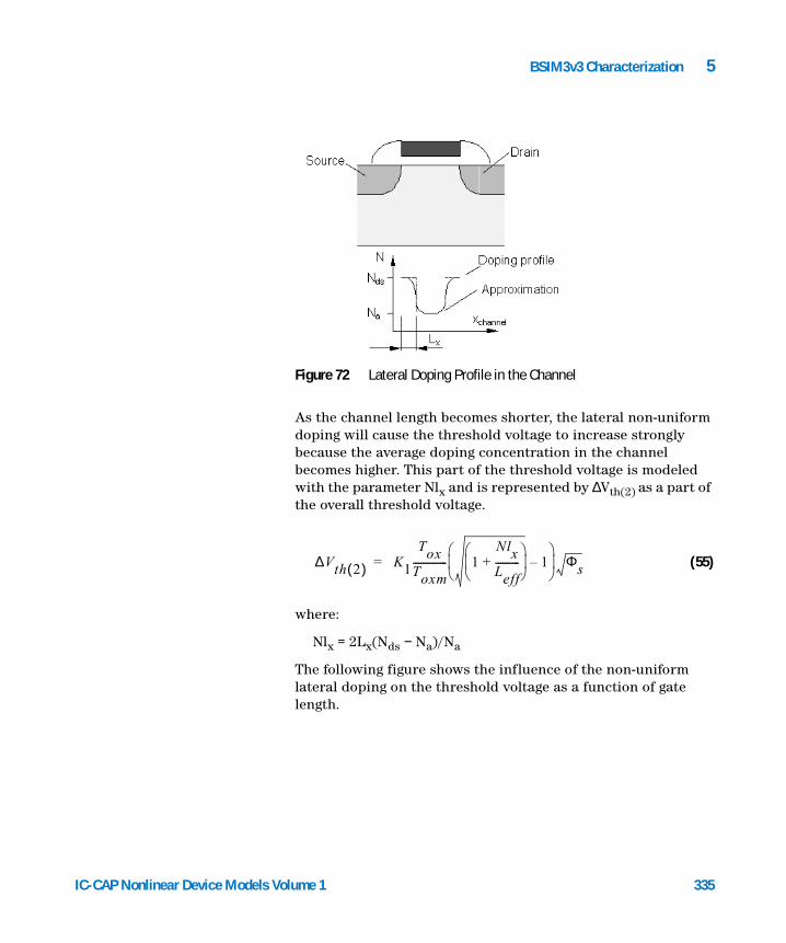
BSIM3v3 Characterization 5
IC-CAP Nonlinear Device Models Vo
As the channel length becomes shorter, the lateral non-uniform doping will cause the threshold voltage to increase strongly because the average doping concentration in the channel becomes higher. This part of the threshold voltage is modeled with the parameter Nlx and is represented by ∆Vth(2) as a part of the overall threshold voltage.
(55)
where:
Nlx = 2Lx(Nds − Na)/Na
The following figure shows the influence of the non-uniform lateral doping on the threshold voltage as a function of gate length.
Figure 72 Lateral Doping Profile in the Channel
∆Vth 2( ) K1
ToxToxm-------------- 1
NlxLeff----------+
1–
Φs=
lume 1 335
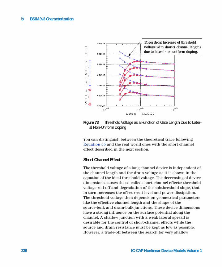
336
5 BSIM3v3 Characterization
You can distinguish between the theoretical trace following Equation 55 and the real world ones with the short channel effect described in the next section.
Short Channel Effect
The threshold voltage of a long channel device is independent of the channel length and the drain voltage as it is shown in the equation of the ideal threshold voltage. The decreasing of device dimensions causes the so-called short-channel effects: threshold voltage roll-off and degradation of the subthreshold slope, that in turn increases the off-current level and power dissipation. The threshold voltage then depends on geometrical parameters like the effective channel length and the shape of the source-bulk and drain-bulk junctions. These device dimensions have a strong influence on the surface potential along the channel. A shallow junction with a weak lateral spread is desirable for the control of short-channel effects while the source and drain resistance must be kept as low as possible. However, a trade-off between the search for very shallow
Figure 73 Threshold Voltage as a Function of Gate Length Due to Later-al Non-Uniform Doping
IC-CAP Nonlinear Device Models Volume 1
BSIM3v3 Characterization 5
IC-CAP Nonlinear Device Models Vo
junctions and the degradation of the maximum achievable current through the parasitic resistance of low doped drain regions must be found.
Those effects can be shown in device simulators, where drift, diffusion, and additionally the hot electron behavior can be simulated. The following equations are responsible for the modeling of the short channel effect part ∆Vth(3) in the BSIM3 model:
(56)
(57)
(58)
where:
Vbi built-in voltage of the PN junction between the source/drain and the substrate
=
Nd = source/drain doping concentration (or in the LDD regions) if they exist
DVT0, DVT1, DVT2 are parameters used to make the model fit different technologies
∆Vth 3( ) DVT0 e
DVT1 Leff2lt
----------–
2e
DVT1
Lefflt
----------–
+ Vbi Φs–( )=
lr
εsiToxXdep
εsio2------------------------------ 1 DVT2Vbseff+( )=
Xdep
2εsi Φs Vbseff–( )
qNch---------------------------------------------=
KBT
q-----------
NchNd
ni2
-----------------
ln
lume 1 337
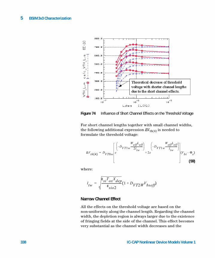
338
5 BSIM3v3 Characterization
For short channel lengths together with small channel widths, the following additional expression ∆Vth(4) is needed to formulate the threshold voltage:
(59)
where:
Narrow Channel Effect
All the effects on the threshold voltage are based on the non-uniformity along the channel length. Regarding the channel width, the depletion region is always larger due to the existence of fringing fields at the side of the channel. This effect becomes very substantial as the channel width decreases and the
Figure 74 Influence of Short Channel Effects on the Threshold Voltage
∆Vth 4( ) DVT0w e
DVT1w
WeffLeff2ltw
-----------------------–
2e
DVT1w
WeffLeffltw
-----------------------–
+ Vbi Φs–( )=
ltw
εsiToxXdepεsio2
------------------------------ 1 DVT2WVbseff+( )=
IC-CAP Nonlinear Device Models Volume 1
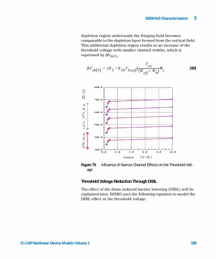
BSIM3v3 Characterization 5
IC-CAP Nonlinear Device Models Vo
depletion region underneath the fringing field becomes comparable to the depletion layer formed from the vertical field. This additional depletion region results in an increase of the threshold voltage with smaller channel widths, which is expressed by ∆Vth(5).
(60)
Threshold Voltage Reduction Through DIBL
The effect of the drain induced barrier lowering (DIBL) will be explained later. BSIM3 uses the following equation to model the DIBL effect in the threshold voltage:
Figure 75 Influence of Narrow Channel Effects on the Threshold Volt-age
∆Vth 5( ) K3 K3bVbseff+( )Tox
Weff W0+( )-------------------------------Φs=
lume 1 339
340
5 BSIM3v3 Characterization
(61)
(62)
∆Vth 6( ) e
Dsub
Leff2lt0----------–
2e
Dsub
Lefflt0
----------–
+ Eta0 EtabVbseff+( )Vds=
lt0
εsiToxXdepεsio2
------------------------------=
Carrier Mobility Reduction
BSIM3v3 provides 3 different equations for the modeling of the mobility reduction. They can be selected by the flag MOBMOD.
MOBMOD=1:
(63)
MOBMOD=2:
(64)
MOBMOD=3:
(65)
The influence of the mobility reduction parameters is demonstrated in the following figure where the simulated drain current with and without mobility reduction is shown.
µeff
µo
1 Ua Uc+ Vbseff( ) Vgsteff 2Vth+( ) Tox⁄( ) Ub Vgsteff 2Vth+( ) Tox⁄( )2
+ +----------------------------------------------------------------------------------------------------------------------------------------------------------------------------------------------------=
µeff
µ0
1 Ua Uc+ Vbseff( ) Vgsteff Tox⁄( ) Ub Vgsteff Tox⁄( )2
+ +----------------------------------------------------------------------------------------------------------------------------------------------------=
µeff
µ0
1 Ua Vgsteff 2Vth+( ) Tox⁄ Ub Vgsteff 2Vth+( ) Tox⁄( )2
+ 1 Uc Vbseff+( )+
--------------------------------------------------------------------------------------------------------------------------------------------------------------------------------------------------------=
IC-CAP Nonlinear Device Models Volume 1
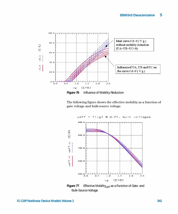
BSIM3v3 Characterization 5
IC-CAP Nonlinear Device Models Vo
The following figure shows the effective mobility as a function of gate voltage and bulk-source voltage.
Figure 76 Influence of Mobility Reduction
Figure 77 Effective Mobilityµeff as a Function of Gate- and
Bulk-Source-Voltage
lume 1 341
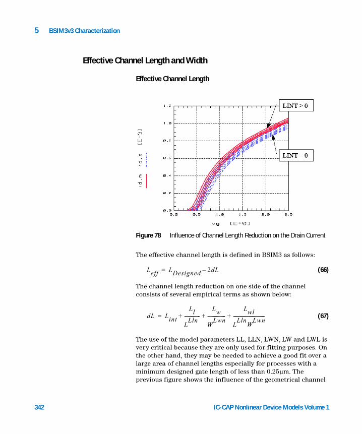
5 BSIM3v3 Characterization
Effective Channel Length and Width
342
Effective Channel Length
The effective channel length is defined in BSIM3 as follows:
(66)
The channel length reduction on one side of the channel consists of several empirical terms as shown below:
(67)
The use of the model parameters LL, LLN, LWN, LW and LWL is very critical because they are only used for fitting purposes. On the other hand, they may be needed to achieve a good fit over a large area of channel lengths especially for processes with a minimum designed gate length of less than 0.25µm. The previous figure shows the influence of the geometrical channel
Figure 78 Influence of Channel Length Reduction on the Drain Current
Leff LDesigned 2dL–=
dL Lint
Ll
LLln
--------------Lw
WLwn
----------------Lwl
LLln
WLwn
----------------------------+ + +=
IC-CAP Nonlinear Device Models Volume 1
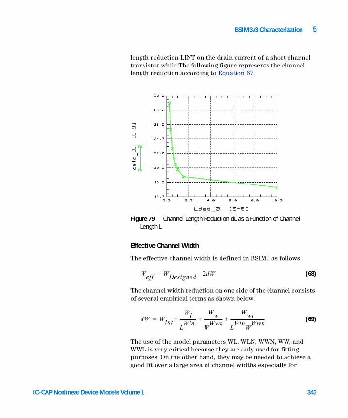
BSIM3v3 Characterization 5
IC-CAP Nonlinear Device Models Vo
length reduction LINT on the drain current of a short channel transistor while The following figure represents the channel length reduction according to Equation 67.
Effective Channel Width
The effective channel width is defined in BSIM3 as follows:
(68)
The channel width reduction on one side of the channel consists of several empirical terms as shown below:
(69)
The use of the model parameters WL, WLN, WWN, WW, and WWL is very critical because they are only used for fitting purposes. On the other hand, they may be needed to achieve a good fit over a large area of channel widths especially for
Figure 79 Channel Length Reduction dL as a Function of Channel Length L
Weff WDesigned 2dW–=
dW Wint
Wl
LWln
---------------Ww
WWwn
-----------------Wwl
LWln
WWwn
--------------------------------+ + +=
lume 1 343
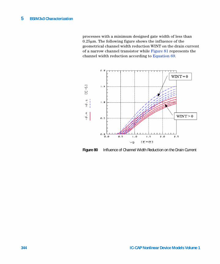
344
5 BSIM3v3 Characterization
processes with a minimum designed gate width of less than 0.25µm. The following figure shows the influence of the geometrical channel width reduction WINT on the drain current of a narrow channel transistor while Figure 81 represents the channel width reduction according to Equation 69.
Figure 80 Influence of Channel Width Reduction on the Drain Current
IC-CAP Nonlinear Device Models Volume 1
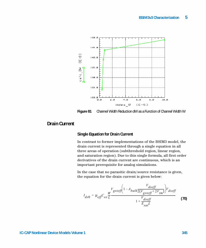
BSIM3v3 Characterization 5
IC-CAP Nonlinear Device Models Vo
Figure 81 Channel Width Reduction dW as a Function of Channel Width W
Drain CurrentSingle Equation for Drain Current
In contrast to former implementations of the BSIM3 model, the drain current is represented through a single equation in all three areas of operation (subthreshold region, linear region, and saturation region). Due to this single formula, all first order derivatives of the drain current are continuous, which is an important prerequisite for analog simulations.
In the case that no parasitic drain/source resistance is given, the equation for the drain current is given below:
(70)Ids0 µeffCox
WL-----
Vgsteff 1 Abulk
Vdseff2 Vgsteff 2Vtm+( )----------------------------------------------–
Vdseff
1VdseffEsatL----------------+
-----------------------------------------------------------------------------------------------------------------=
lume 1 345
346
5 BSIM3v3 Characterization
This equation is valid for all three regions of operation of the MOS transistor because the voltages at drain, gate and bulk are replaced by effective drain voltage Vdseff, the effective gate voltage Vgsteff and the effective bulk voltage Vbseff, which are all defined by the continuous equations below:
Equation 71 shows the effective (Vgs - Vth) voltage, where the factor n is defined in Equation 75.
(71)
The figure above shows Vgsteff in logarithmic scale. Vgsteff fits a linear function for values of Vgs greater than Vth while the subthreshold area is covered by the fit of an exponential
Figure 82 Effective Voltage Vgs - Vth
Vgsteff
2nνt ln 1Vgs Vth–
2nνt------------------------
exp+
1 2nCox
2Φsq εsiNch( )--------------------------
Vgs Vth– 2Voff–
2nνt--------------------------------------------–
exp+
------------------------------------------------------------------------------------------------------------------------=
IC-CAP Nonlinear Device Models Volume 1
BSIM3v3 Characterization 5
IC-CAP Nonlinear Device Models Vo
function. Through this equation the first derivative is continuous between both operational regions (subthreshold and linear) of the MOS transistor.
Equation 72 shows the effective drain source voltage, Vdseff:
(72)
The following figure shows Vdseff in both the linear and the saturation region of operation of the MOS transistor. Vdseff models the transition between linear and saturation region without discontinuity in the first derivative of the drain current.
Drain Saturation Voltage Vdsat
The equation for the drain saturation voltage is divided into two cases, the intrinsic case with Rds = 0 and the extrinsic case with Rds > 0:
Figure 83 Effective Voltage Vdseff
Vdseff Vdsat12--- Vdsat Vds δ– Vdsat Vds δ––( )2 4δVdsat++– –=
lume 1 347
348
5 BSIM3v3 Characterization
(73)
where
The influence of the maximum carrier velocity VSAT on the drain current Ids and the conductance gds is demonstrated in the following figure.
Figure 84 Influence of VSAT on Drain Current Ids and Conductance gds
Vdsat
Esat Leff Vgsteff 2Vtm+( )
AbulkEsatLeff Vgsteff 2Vtm+( )+--------------------------------------------------------------------------------------- Rds 0=,
b b2
4– ac––2a
--------------------------------- Rds 0≠,
=
a Abulk2
RdsCoxWνsat1λ--- 1– Abulk+=
b Vgsteff 2Vtm+( ) 2λ--- 1– –
AbulkEsatLeff3AbulkRdsCoxWνsat Vgsteff 2Vtm+( )++
=
c EsatLeff Vgsteff 2Vtm+( ) 2RdsCoxWνsat Vgsteff 2Vtm+( )2
+=
IC-CAP Nonlinear Device Models Volume 1

BSIM3v3 Characterization 5
IC-CAP Nonlinear Device Models Vo
Bulk Charge Effect
When the drain voltage is high, combined with a long channel length, the depletion depth of the channel is not uniform along the channel length. This will cause the threshold voltage to vary along the channel length and is called bulk charge effect. The following figure shows the depletion depth as a function of channel length. For long channels, this effect causes a reduction of the drain current.
The bulk charge effect Abulk is modeled in BSIM3 with the parameters A0, AGS, B0, B1, and KETA as shown in Equation 74.
(74)
The influence on the drain current is shown in the following figure.
Figure 85 Depletion Width along the Channel Length
ulk 1
K1
ToxToxm--------------
2 Φs Vbseff–-------------------------------------+
B0Weff B1+-------------------------
A0 Leff
Leff 2 XJ Xdep+-----------------------------------------------+
1 AGS Vgsteff
Leff
Leff 2 XJ Xdep+----------------------------------------------- 2
–
11 KetaV+-------------------------=
lume 1 349
350
5 BSIM3v3 Characterization
Drain Current in the Subthreshold RegionThe drain current in the subthreshold region is modeled in BSIM3v3 by the effective voltage Vgsteff. The model parameters VOFF and NFACTOR describe the subthreshold current for a large transistor, while the parameters CDSC, CDSCD, and CDSCB are responsible for modeling the subthreshold behavior as a function of channel length. All these parameters contribute to the factor n in the formula for Vgsteff (see Equation 71).
(75)
(76)
The influence of VOFF and NFACTOR on the drain current in the subthreshold region is shown in the following figure.
Figure 86 Influence of A0 and KETA on Ids at High Drain Voltages
n 1 Nfactor
CdCox----------
Cdsc Cdscd Vds Cdscb Vbseff++( )
Cox---------------------------------------------------------------------------------------------θth
CitCox----------++ +=
θth e
DVT1 Leff2lt
----------–
2e
DVT1
Lefflt
----------–
+=
IC-CAP Nonlinear Device Models Volume 1
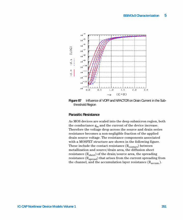
BSIM3v3 Characterization 5
IC-CAP Nonlinear Device Models Vo
Parasitic Resistance
As MOS devices are scaled into the deep submicron region, both the conductance gm and the current of the device increase. Therefore the voltage drop across the source and drain series resistance becomes a non-negligible fraction of the applied drain source voltage. The resistance components associated with a MOSFET structure are shown in the following figure. These include the contact resistance (Rcontact) between metallization and source/drain area, the diffusion sheet resistance (Rsheet) of the drain/source area, the spreading resistance (Rspread) that arises from the current spreading from the channel, and the accumulation layer resistance (Raccum.).
Figure 87 Influence of VOFF and NFACTOR on Drain Current in the Sub-threshold Region
lume 1 351
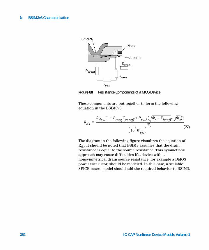
352
5 BSIM3v3 Characterization
These components are put together to form the following equation in the BSIM3v3:
(77)
The diagram in the following figure visualizes the equation of Rds. It should be noted that BSIM3 assumes that the drain resistance is equal to the source resistance. This symmetrical approach may cause difficulties if a device with a nonsymmetrical drain source resistance, for example a DMOS power transistor, should be modeled. In this case, a scalable SPICE macro model should add the required behavior to BSIM3.
Figure 88 Resistance Components of a MOS Device
Rds
Rdsw 1 PrwgVgsteff Prwb Φs Vbseff– Φs–( )++[ ]
106
Weff
Wr----------------------------------------------------------------------------------------------------------------------------------------=
IC-CAP Nonlinear Device Models Volume 1

BSIM3v3 Characterization 5
IC-CAP Nonlinear Device Models Vo
With this enhancement, Equation 70 for the drain current can be rewritten:(78)
The influence of the parasitic resistance on the drain current is demonstrated for a SHORT and a SMALL transistor in the following figure.
Figure 89 Drain Source Resistance Rds as a Function of Vg and Vb
Ids
Ids01 RdsIds0 Vdseff⁄+----------------------------------------------------=
lume 1 353
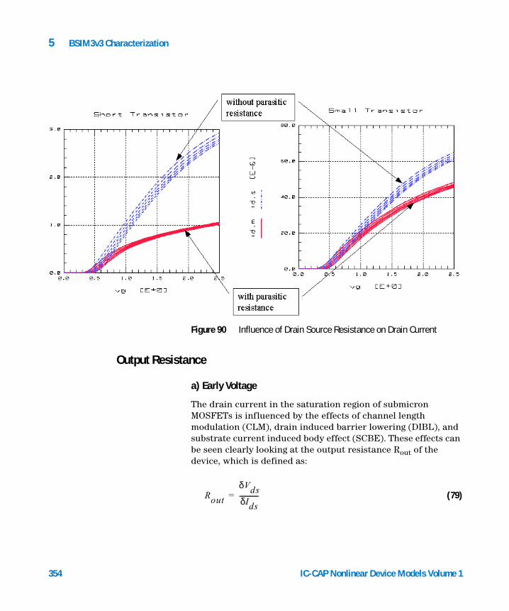
354
5 BSIM3v3 Characterization
Figure 90 Influence of Drain Source Resistance on Drain Current
Output Resistance
a) Early Voltage
The drain current in the saturation region of submicron MOSFETs is influenced by the effects of channel length modulation (CLM), drain induced barrier lowering (DIBL), and substrate current induced body effect (SCBE). These effects can be seen clearly looking at the output resistance Rout of the device, which is defined as:
(79)Rout
δVdsδIds------------=
IC-CAP Nonlinear Device Models Volume 1
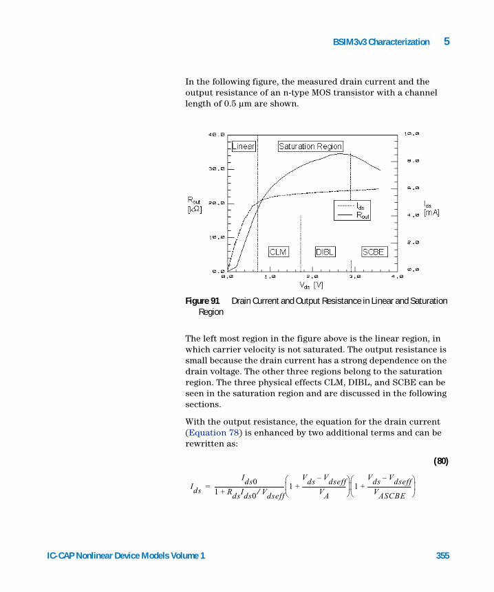
BSIM3v3 Characterization 5
IC-CAP Nonlinear Device Models Vo
In the following figure, the measured drain current and the output resistance of an n-type MOS transistor with a channel length of 0.5 µm are shown.
The left most region in the figure above is the linear region, in which carrier velocity is not saturated. The output resistance is small because the drain current has a strong dependence on the drain voltage. The other three regions belong to the saturation region. The three physical effects CLM, DIBL, and SCBE can be seen in the saturation region and are discussed in the following sections.
With the output resistance, the equation for the drain current (Equation 78) is enhanced by two additional terms and can be rewritten as:
(80)
Figure 91 Drain Current and Output Resistance in Linear and Saturation Region
Ids
Ids01 RdsIds0 Vdseff⁄+--------------------------------------------------- 1
Vds Vdseff–
VA--------------------------------+
1Vds Vdseff–
VASCBE--------------------------------+
=
lume 1 355
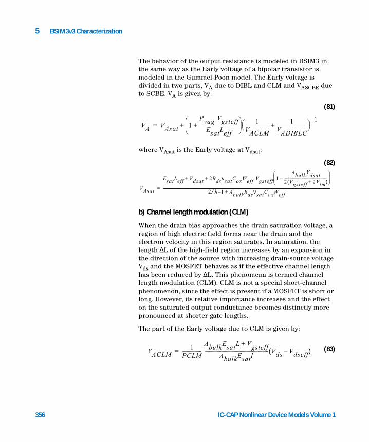
356
5 BSIM3v3 Characterization
The behavior of the output resistance is modeled in BSIM3 in the same way as the Early voltage of a bipolar transistor is modeled in the Gummel-Poon model. The Early voltage is divided in two parts, VA due to DIBL and CLM and VASCBE due to SCBE. VA is given by:
(81)
where VAsat is the Early voltage at Vdsat:
(82)
b) Channel length modulation (CLM)
When the drain bias approaches the drain saturation voltage, a region of high electric field forms near the drain and the electron velocity in this region saturates. In saturation, the length ∆L of the high-field region increases by an expansion in the direction of the source with increasing drain-source voltage Vds and the MOSFET behaves as if the effective channel length has been reduced by ∆L. This phenomena is termed channel length modulation (CLM). CLM is not a special short-channel phenomenon, since the effect is present if a MOSFET is short or long. However, its relative importance increases and the effect on the saturated output conductance becomes distinctly more pronounced at shorter gate lengths.
The part of the Early voltage due to CLM is given by:
(83)
VA VAsat 1Pvag Vgsteff
EsatLeff----------------------------------+
1
VACLM--------------------
1VADIBLC--------------------------+
1–+=
VAsat
EsatLeff Vdsat 2RdsνsatCoxWeff Vgsteff 1AbulkVdsat
2 Vgsteff 2Vtm+( )-----------------------------------------------–
+ +
2 λ 1– AbulkRdsνsatCoxWeff+⁄---------------------------------------------------------------------------------------------------------------------------------------------------------------------------------------=
VACLM1
PCLM-----------------
AbulkEsatL Vgsteff+
AbulkEsatl-------------------------------------------------------- Vds Vdseff–( )=
IC-CAP Nonlinear Device Models Volume 1
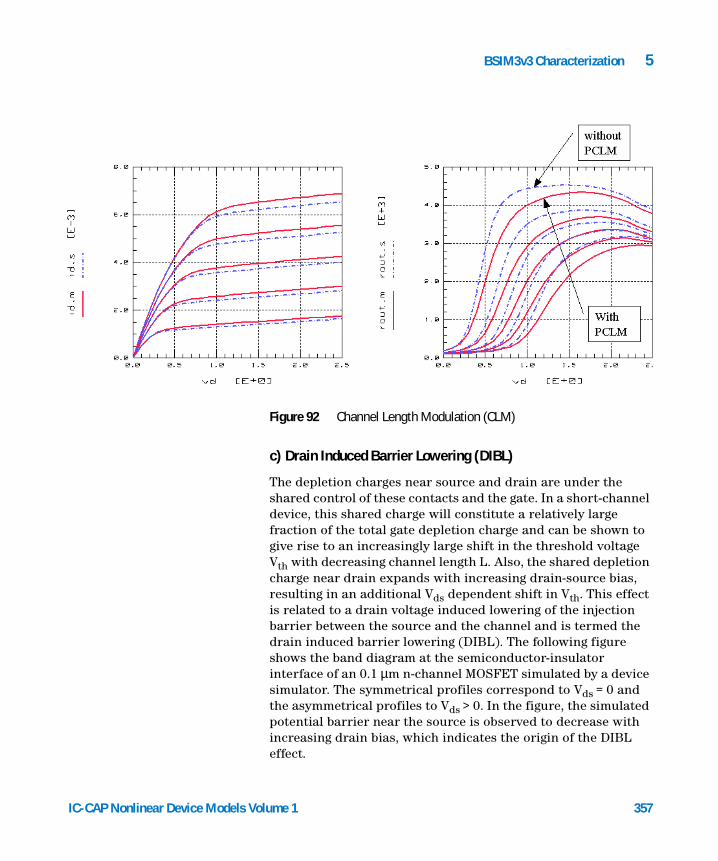
BSIM3v3 Characterization 5
IC-CAP Nonlinear Device Models Vo
c) Drain Induced Barrier Lowering (DIBL)
The depletion charges near source and drain are under the shared control of these contacts and the gate. In a short-channel device, this shared charge will constitute a relatively large fraction of the total gate depletion charge and can be shown to give rise to an increasingly large shift in the threshold voltage Vth with decreasing channel length L. Also, the shared depletion charge near drain expands with increasing drain-source bias, resulting in an additional Vds dependent shift in Vth. This effect is related to a drain voltage induced lowering of the injection barrier between the source and the channel and is termed the drain induced barrier lowering (DIBL). The following figure shows the band diagram at the semiconductor-insulator interface of an 0.1 µm n-channel MOSFET simulated by a device simulator. The symmetrical profiles correspond to Vds = 0 and the asymmetrical profiles to Vds > 0. In the figure, the simulated potential barrier near the source is observed to decrease with increasing drain bias, which indicates the origin of the DIBL effect.
Figure 92 Channel Length Modulation (CLM)
lume 1 357
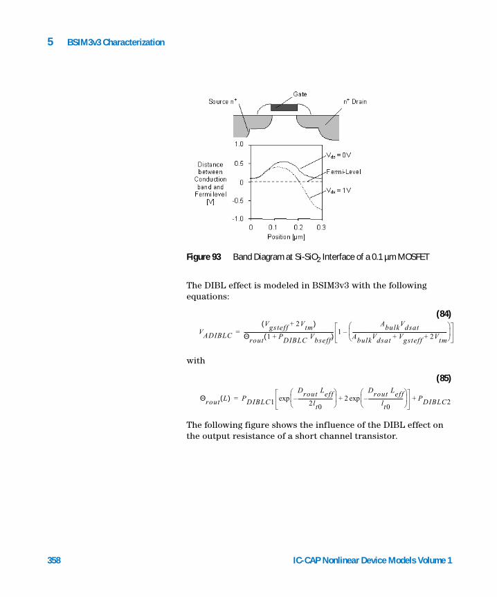
358
5 BSIM3v3 Characterization
The DIBL effect is modeled in BSIM3v3 with the following equations:
(84)
with
(85)
The following figure shows the influence of the DIBL effect on the output resistance of a short channel transistor.
Figure 93 Band Diagram at Si-SiO2 Interface of a 0.1 µm MOSFET
VADIBLC
Vgsteff 2Vtm+( )
Θrout 1 PDIBLC Vbseff+( )------------------------------------------------------------------------- 1AbulkVdsat
AbulkVdsat Vgsteff 2Vtm+ +-----------------------------------------------------------------------------
–=
Θrout L( ) PDIBLC1
Drout Leff2lt0
----------------------------–
2Drout Leff
lt0----------------------------–
exp+exp PDIBLC2+=
IC-CAP Nonlinear Device Models Volume 1
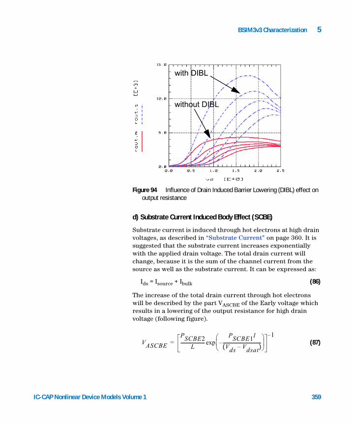
BSIM3v3 Characterization 5
IC-CAP Nonlinear Device Models Vo
d) Substrate Current Induced Body Effect (SCBE)Substrate current is induced through hot electrons at high drain voltages, as described in “Substrate Current” on page 360. It is suggested that the substrate current increases exponentially with the applied drain voltage. The total drain current will change, because it is the sum of the channel current from the source as well as the substrate current. It can be expressed as:
Ids = Isource + Ibulk (86)
The increase of the total drain current through hot electrons will be described by the part VASCBE of the Early voltage which results in a lowering of the output resistance for high drain voltage (following figure).
(87)
Figure 94 Influence of Drain Induced Barrier Lowering (DIBL) effect on output resistance
with DIBL
without DIBL
VASCBE
PSCBE2L
----------------------PSCBE1l
Vds Vdsat–( )-----------------------------------–
exp1–
=
lume 1 359
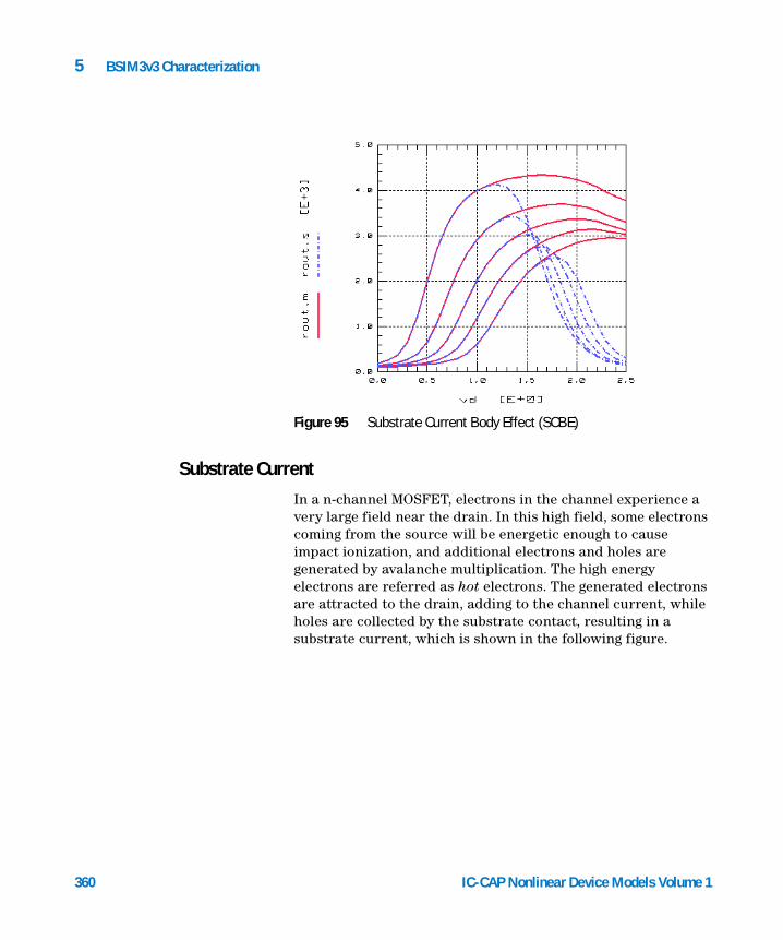
360
5 BSIM3v3 Characterization
Figure 95 Substrate Current Body Effect (SCBE)
Substrate Current
In a n-channel MOSFET, electrons in the channel experience a very large field near the drain. In this high field, some electrons coming from the source will be energetic enough to cause impact ionization, and additional electrons and holes are generated by avalanche multiplication. The high energy electrons are referred as hot electrons. The generated electrons are attracted to the drain, adding to the channel current, while holes are collected by the substrate contact, resulting in a substrate current, which is shown in the following figure.
IC-CAP Nonlinear Device Models Volume 1
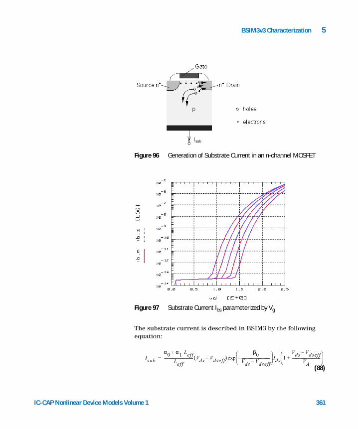
BSIM3v3 Characterization 5
IC-CAP Nonlinear Device Models Vo
The substrate current is described in BSIM3 by the following equation:(88)
Figure 96 Generation of Substrate Current in an n-channel MOSFET
Figure 97 Substrate Current Ibs parameterized by Vg
Isub
α0 α1 Leff+
Leff--------------------------------- Vds Vdseff–( )
β0Vds Vdseff–--------------------------------–
Ids 1Vds Vdseff–
VA--------------------------------+
exp=
lume 1 361
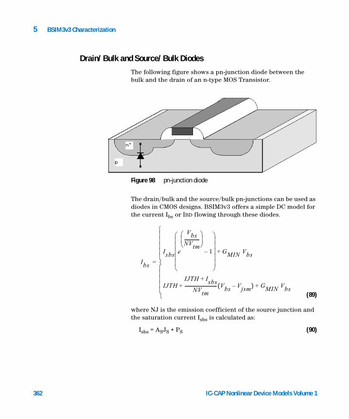
5 BSIM3v3 Characterization
Drain/Bulk and Source/Bulk Diodes
362
The following figure shows a pn-junction diode between the bulk and the drain of an n-type MOS Transistor.
The drain/bulk and the source/bulk pn-junctions can be used as diodes in CMOS designs. BSIM3v3 offers a simple DC model for the current Ibs or IBD flowing through these diodes.
(89)
where NJ is the emission coefficient of the source junction and the saturation current Isbs is calculated as:
Isbs = ASJS + PS (90)
Figure 98 pn-junction diode
Ibs
Isbs e
VbsNVtm--------------
1–
GMIN Vbs+
IJTHIJTH Isbs+
NVtm------------------------------ Vbs Vjsm–( ) GMIN Vbs+ +
=
IC-CAP Nonlinear Device Models Volume 1
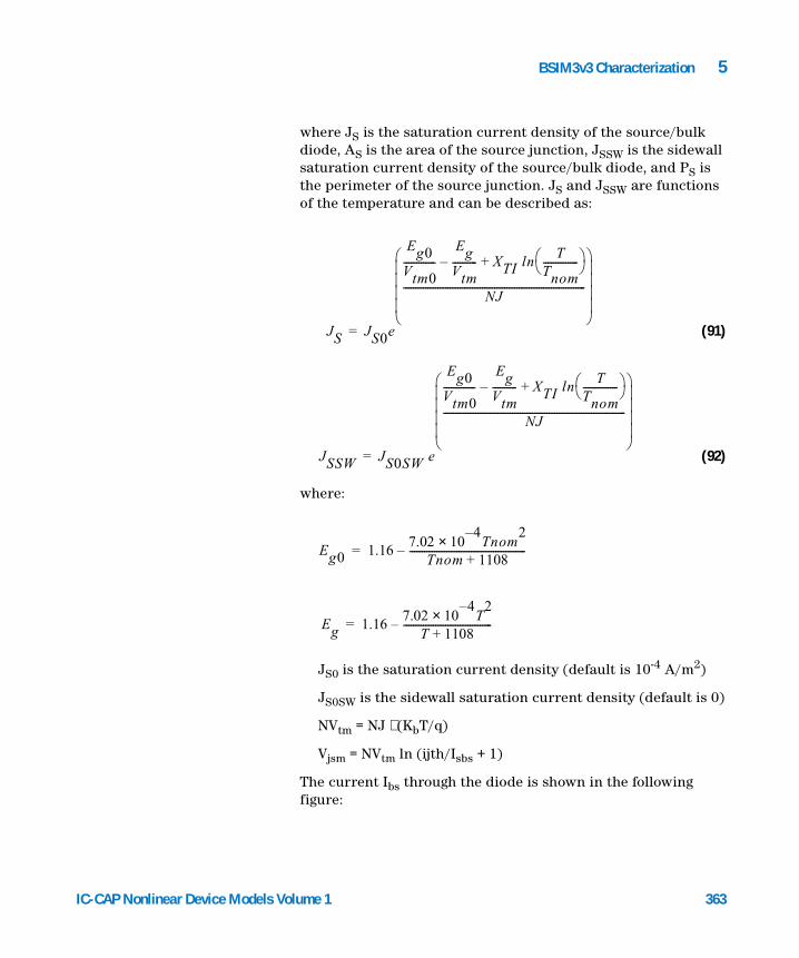
BSIM3v3 Characterization 5
IC-CAP Nonlinear Device Models Vo
where JS is the saturation current density of the source/bulk diode, AS is the area of the source junction, JSSW is the sidewall saturation current density of the source/bulk diode, and PS is the perimeter of the source junction. JS and JSSW are functions of the temperature and can be described as:
(91)
(92)
where:
JS0 is the saturation current density (default is 10-4 A/m2)
JS0SW is the sidewall saturation current density (default is 0)
NVtm = NJ ⋅ (KbT/q)
Vjsm = NVtm ln (ijth/Isbs + 1)
The current Ibs through the diode is shown in the following figure:
JS JS0e
Eg0Vtm0-------------
EgVtm----------– XTI ln
TTnom-------------- +
NJ--------------------------------------------------------------------------
=
JSSW JS0SW e
Eg0Vtm0-------------
EgVtm----------– XTI ln
TTnom-------------- +
NJ--------------------------------------------------------------------------
=
Eg0 1.167.02 10
4–Tnom
2×Tnom 1108+
-----------------------------------------------–=
Eg 1.167.02 10
4–T
2×T 1108+
------------------------------------–=
lume 1 363
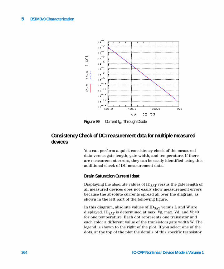
364
5 BSIM3v3 Characterization
Figure 99 Current Ibs Through Diode
Consistency Check of DC measurement data for multiple measured devices
You can perform a quick consistency check of the measured data versus gate length, gate width, and temperature. If there are measurement errors, they can be easily identified using this additional check of DC measurement data.
Drain Saturation Current Idsat
Displaying the absolute values of IDSAT versus the gate length of all measured devices does not easily show measurement errors because the absolute currents spread all over the diagram, as shown in the left part of the following figure.
In this diagram, absolute values of IDSAT versus L and W are displayed. IDSAT is determined at max. Vg, max. Vd, and Vb=0 for one temperature. Each dot represents one transistor and each color a different value of the transistors gate width W. The legend is shown to the right of the plot. If you select one of the dots, at the top of the plot the details of this specific transistor
IC-CAP Nonlinear Device Models Volume 1
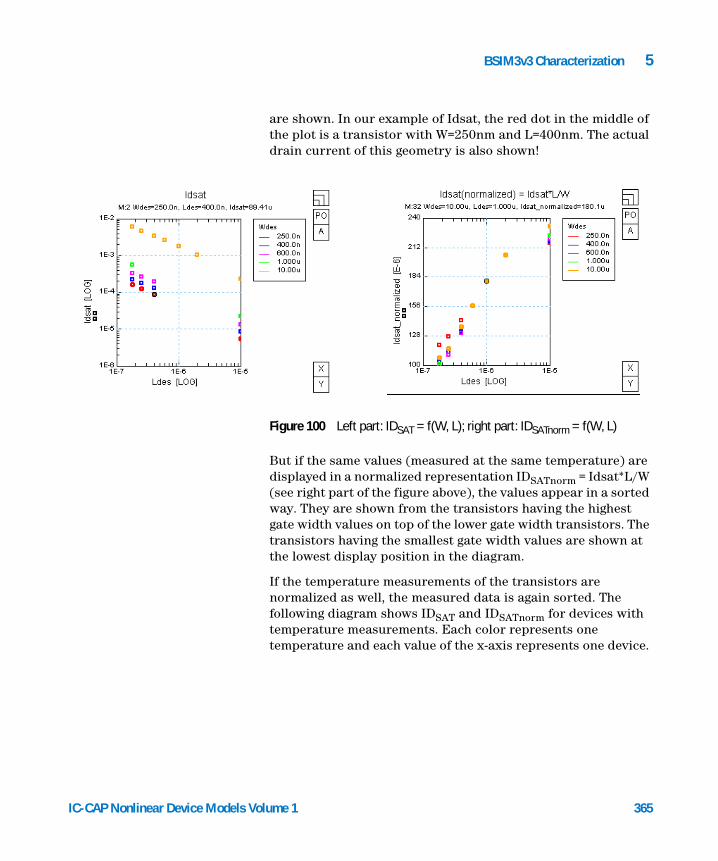
BSIM3v3 Characterization 5
IC-CAP Nonlinear Device Models Vo
are shown. In our example of Idsat, the red dot in the middle of the plot is a transistor with W=250nm and L=400nm. The actual drain current of this geometry is also shown!
Figure 100 Left part: IDSAT = f(W, L); right part: IDSATnorm = f(W, L)But if the same values (measured at the same temperature) are displayed in a normalized representation IDSATnorm = Idsat*L/W (see right part of the figure above), the values appear in a sorted way. They are shown from the transistors having the highest gate width values on top of the lower gate width transistors. The transistors having the smallest gate width values are shown at the lowest display position in the diagram.
If the temperature measurements of the transistors are normalized as well, the measured data is again sorted. The following diagram shows IDSAT and IDSATnorm for devices with temperature measurements. Each color represents one temperature and each value of the x-axis represents one device.
lume 1 365
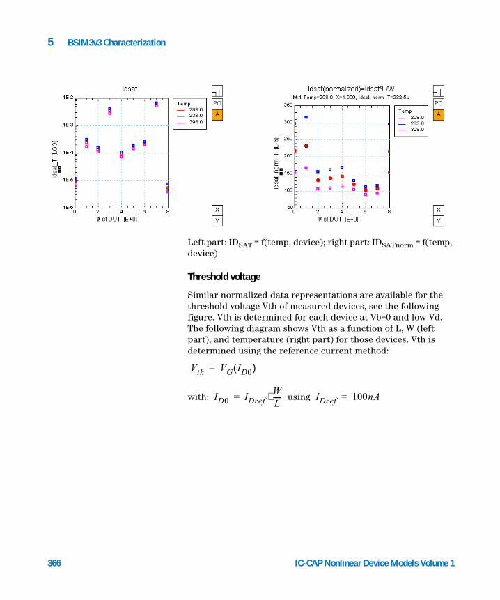
366
5 BSIM3v3 Characterization
Left part: IDSAT = f(temp, device); right part: IDSATnorm = f(temp, device)
Threshold voltage
Similar normalized data representations are available for the threshold voltage Vth of measured devices, see the following figure. Vth is determined for each device at Vb=0 and low Vd. The following diagram shows Vth as a function of L, W (left part), and temperature (right part) for those devices. Vth is determined using the reference current method:
with: using
Vth VG ID0( )=
ID0 IDrefWL-----⋅= IDref 100nA=
IC-CAP Nonlinear Device Models Volume 1
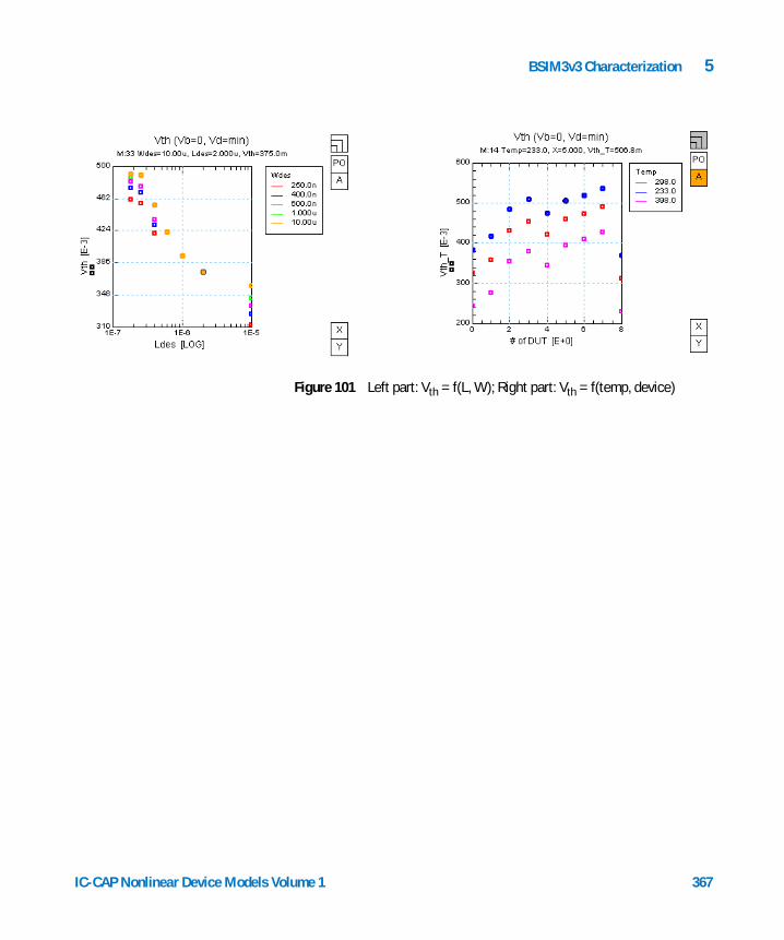
BSIM3v3 Characterization 5
IC-CAP Nonlinear Device Models Vo
Figure 101 Left part: Vth = f(L, W); Right part: Vth = f(temp, device)
lume 1 367
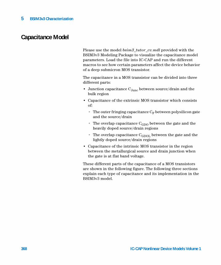
5 BSIM3v3 Characterization
Capacitance Model
368
Please use the model bsim3_tutor_cv.mdl provided with the BSIM3v3 Modeling Package to visualize the capacitance model parameters. Load the file into IC-CAP and run the different macros to see how certain parameters affect the device behavior of a deep submicron MOS transistor.
The capacitance in a MOS transistor can be divided into three different parts:
• Junction capacitance CJunc between source/drain and the bulk region
• Capacitance of the extrinsic MOS transistor which consists of:
• The outer fringing capacitance CF between polysilicon gate and the source/drain
• The overlap capacitance CGDO between the gate and the heavily doped source/drain regions
• The overlap capacitance CGDOL between the gate and the lightly doped source/drain regions
• Capacitance of the intrinsic MOS transistor in the region between the metallurgical source and drain junction when the gate is at flat band voltage.
These different parts of the capacitance of a MOS transistors are shown in the following figure. The following three sections explain each type of capacitance and its implementation in the BSIM3v3 model.
IC-CAP Nonlinear Device Models Volume 1
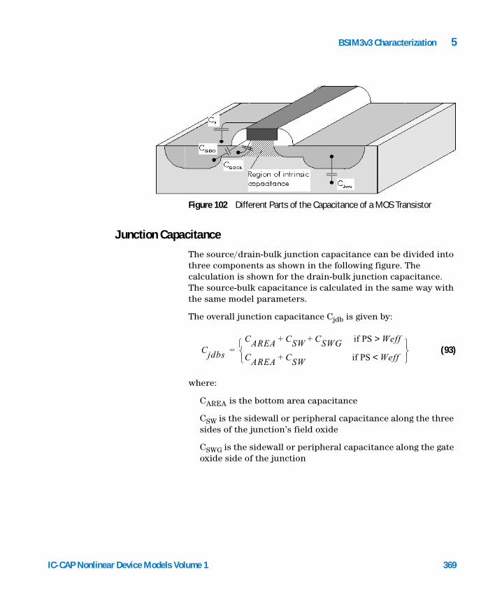
BSIM3v3 Characterization 5
IC-CAP Nonlinear Device Models Vo
Figure 102 Different Parts of the Capacitance of a MOS Transistor
Junction Capacitance
The source/drain-bulk junction capacitance can be divided into three components as shown in the following figure. The calculation is shown for the drain-bulk junction capacitance. The source-bulk capacitance is calculated in the same way with the same model parameters.
The overall junction capacitance Cjdb is given by:
(93)
where:
CAREA is the bottom area capacitance
CSW is the sidewall or peripheral capacitance along the three sides of the junction’s field oxide
CSWG is the sidewall or peripheral capacitance along the gate oxide side of the junction
Cjdbs
CAREA CSW CSWG if PS Weff> + +
CAREA CSW if PS Weff<+
=
lume 1 369
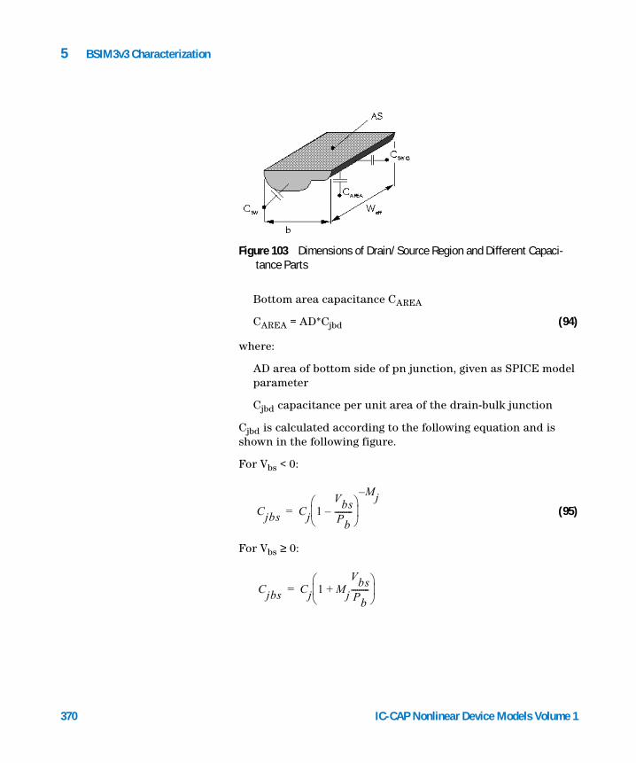
370
5 BSIM3v3 Characterization
Bottom area capacitance CAREA
CAREA = AD*Cjbd (94)
where:
AD area of bottom side of pn junction, given as SPICE model parameter
Cjbd capacitance per unit area of the drain-bulk junction
Cjbd is calculated according to the following equation and is shown in the following figure.
For Vbs < 0:
(95)
For Vbs ≥ 0:
Figure 103 Dimensions of Drain/Source Region and Different Capaci-tance Parts
Cjbs Cj 1VbsPb---------–
M– j=
Cjbs Cj 1 Mj
VbsPb---------+
=
IC-CAP Nonlinear Device Models Volume 1
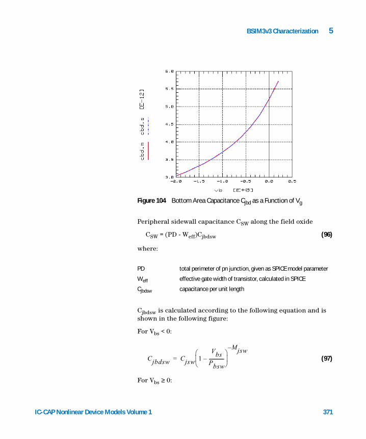
BSIM3v3 Characterization 5
IC-CAP Nonlinear Device Models Vo
Peripheral sidewall capacitance CSW along the field oxideCSW = (PD - Weff)Cjbdsw (96)
where:
Cjbdsw is calculated according to the following equation and is shown in the following figure:
For Vbs < 0:
(97)
For Vbs ≥ 0:
Figure 104 Bottom Area Capacitance Cjbd as a Function of Vg
PD total perimeter of pn junction, given as SPICE model parameter
Weff effective gate width of transistor, calculated in SPICE
Cjbdsw capacitance per unit length
Cjbdsw Cjsw 1Vbs
Pbsw-------------–
M– jsw=
lume 1 371

372
5 BSIM3v3 Characterization
Peripheral sidewall capacitance CSWG along the gate oxide
CSWG = WeffCjbdswg (98)
where:
Cjbdswg is calculated according to the following equation and is shown in the following figure.
For Vbs < 0:
Figure 105 Sidewall Capacitance Cjbdsw as a Function of Vg
Weff effective gate width of transistor, calculated in SPICE
Cjbdswg capacitance per unit length
Cjbdsw Cjsw 1 Mjsw
VbsPbsw-------------+
=
IC-CAP Nonlinear Device Models Volume 1
BSIM3v3 Characterization 5
IC-CAP Nonlinear Device Models Vo
(99)
For Vbs ≥ 0:
Figure 106 Sidewall Capacitance Cjbdswg Along the Gate Oxide as a
Function of Vg
Cjbs Cjswg 1Vbs
Pbswg-----------------–
M– jswg=
Cjbs Cjswg 1 Mjswg
VbsPbswg-----------------+
=
lume 1 373
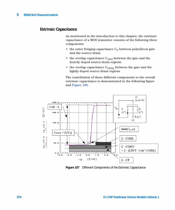
5 BSIM3v3 Characterization
Extrinsic Capacitance
374
As mentioned in the introduction to this chapter, the extrinsic capacitance of a MOS transistor consists of the following three components:
• the outer fringing capacitance CF between polysilicon gate and the source/drain
• the overlap capacitance CGDO between the gate and the heavily doped source/drain regions
• the overlap capacitance CGDOL between the gate and the lightly doped source/drain regions
The contribution of these different components to the overall extrinsic capacitance is demonstrated in the following figure and Figure 108.
Figure 107 Different Components of the Extrinsic Capacitance
IC-CAP Nonlinear Device Models Volume 1
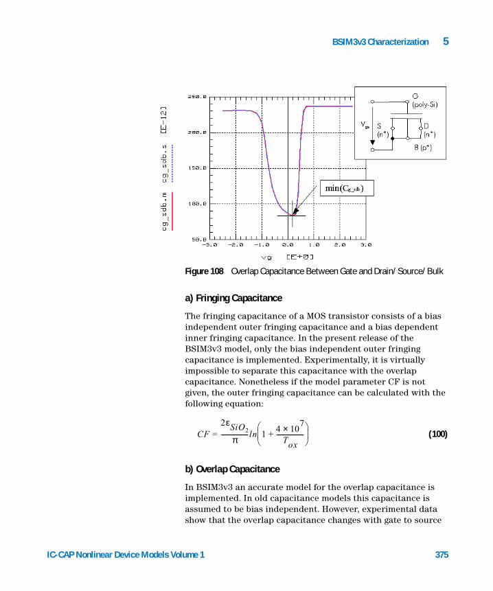
BSIM3v3 Characterization 5
IC-CAP Nonlinear Device Models Vo
a) Fringing CapacitanceThe fringing capacitance of a MOS transistor consists of a bias independent outer fringing capacitance and a bias dependent inner fringing capacitance. In the present release of the BSIM3v3 model, only the bias independent outer fringing capacitance is implemented. Experimentally, it is virtually impossible to separate this capacitance with the overlap capacitance. Nonetheless if the model parameter CF is not given, the outer fringing capacitance can be calculated with the following equation:
(100)
b) Overlap Capacitance
In BSIM3v3 an accurate model for the overlap capacitance is implemented. In old capacitance models this capacitance is assumed to be bias independent. However, experimental data show that the overlap capacitance changes with gate to source
Figure 108 Overlap Capacitance Between Gate and Drain/Source/Bulk
CF2εSiO2
π------------------ ln 1
4 107×
Tox------------------+
=
lume 1 375
376
5 BSIM3v3 Characterization
and gate to drain biases. In a single drain structure or the heavily doped S/D to gate overlap region in a LDD structure, the bias dependence is the result of depleting the surface of the source and drain regions. Since the modulation is expected to be very small, this region can be modeled with a constant capacitance. However in LDD MOSFETs a substantial portion of the LDD region can be depleted, both in the vertical and lateral directions. This can lead to a large reduction of overlap capacitance. This LDD region can be in accumulation or depletion.
In BSIM3v3, a single equation is implemented for both regions by using such smoothing parameters as Vgsoverlap and Vgdoverlap for the source and drain side, respectively. Unlike the case with the intrinsic capacitance, the overlap capacitances are reciprocal. In other words, Cgsoverlap = Csgoverlap and Cgdoverlap = Cdgoverlap.
The model equations for the overlap capacitance are shown for the drain overlap capacitance and are identical for the source overlap capacitance:
Overlap charge per gate width:
(101)
QoverlapWeff
------------------------- CGDOVgs CGDL Vgd Vgd overlap,–CKAPPA
2-------------------------– 1– 1
4Vgd overlap,CKAPPA
-------------------------------------–+
+=
where:
with the smoothing parameter:
(102)
CKAPPA2εsiqNLDO
Cox2
-------------------------------=
Vgd overlap,12--- Vgd δ2+( ) Vgd δ2+( )2 4δ2+–
δ2 2 100⁄
=
=
IC-CAP Nonlinear Device Models Volume 1
BSIM3v3 Characterization 5
IC-CAP Nonlinear Device Models Vo
for the measurement and simulation conditions given in Figure 107, this results in the overlap capacitance:
(103)
The model parameter CGDO in Equation 101 can be calculated by the following equation:
(104)
where DLC represents the channel length reduction in the BSIM3v3 capacitance model. Please see the next section for more details about DLC:
Cgd overlap,∂Qoverlap
∂Vgs----------------------------=
CGDO DLC COX⋅( ) CGDL–=
Intrinsic Capacitance
a) Geometry for Capacitance Model
The BSIM3v3 model uses different expressions for the effective channel length Leff and the effective channel width Weff for the I-V and the C-V parts of the model.
The geometry dependence for the intrinsic capacitance part is given as the following:
(105)
(106)
Lactive and Wactive are the effective length and width of the intrinsic device for capacitance calculations. The parameter ∆L is equal to the source/drain to gate overlap length plus the difference between drawn and actual poly gate length due to processing (gate printing, etching, and oxidation) on one side.
∆W DWCWL
LWLN
----------------WW
WWWN
-------------------WWL
LWLN
WWWN
------------------------------------+ + +=
∆L DLCLL
LLLN
--------------LW
WLWN
------------------LWL
LLLN
WLWN
---------------------------------+ + +=
lume 1 377
378
5 BSIM3v3 Characterization
The Lactive parameter extracted from the capacitance method is a close representation of the metallurgical junction length (physical length).
(107)
(108)
While the authors of the BSIM3v3 model suggest to use a parameter LINT for the I-V model, which is different from DLC, other literature sources [3] propose that LINT should have the same value as DLC. This approach is also implemented in the BSIM3v3 Modeling Package to ensure that the extracted values of the channel length reduction are very close to the real device physics. Therefore, the channel length reduction LINT for the I-V model will be set to DLC from the C-V model extracted from capacitance measurements.
b) Intrinsic Capacitance Model
The intrinsic capacitance model that is implemented in the BSIM3 model is based on the principle of conservation of charge. There are a few major considerations in modeling the intrinsic capacitance of a deep submicron MOS transistor:
Figure 109 Dimensions of a MOSFET
Wactive WDrawn 2∆W–=
Lactive LDrawn 2∆L–=
IC-CAP Nonlinear Device Models Volume 1
BSIM3v3 Characterization 5
IC-CAP Nonlinear Device Models Vo
• The difficulty in capacitance measurement, especially in the deep submicron regime. At very short channel lengths, the MOSFET intrinsic capacitance is very small while the conductance is large.
• Charge can only be measured at high impedance nodes (i.e., the gate and substrate nodes), only 8 of the 16 capacitance components in an intrinsic MOSFET can be directly measured. An alternative solution is to use a 2-D device simulator.
• The access to the internal charges in a simulator.
Therefore, this section presents no details about the intrinsic charge formulations. Please refer to the BSIM3v3 manual [1] for more information. Only the basic principles are described here.
To ensure charge conservation, terminal charges instead of the terminal voltages are used as state variables. The terminal charges Qg, Qb, Qs, and Qd are the charges associated with the gate, bulk, source, and drain. The gate charge is comprised of mirror charges from 3 components:
• The channel minority (inversion) charge (Qinv)
• The channel majority (accumulation) charge (Qacc)
• The substrate fixed charge (Qsub)
The accumulation charge and the substrate charge are associated with the substrate node while the channel charge comes from the source and drain nodes:
(109)
The inversion charges are supplied from the source and drain electrodes. The ratio of Qd and Qs is the charge partitioning ratio. Existing charge partitioning schemes are 0/100, 50/50 and 40/60 (given by the model parameter XPART = 0, 0.5, and 1) which are the ratios of Qd to Qs in the saturation region.
Qg Qsub Qinv Qacc+ +( )–=
Qb Qsub Qacc+=
Qinv Qs Qd+=
lume 1 379
380
5 BSIM3v3 Characterization
From these four terminal charges, 9 transcapacitances C(terminal,voltage) are calculated inside the BSIM3 model as partial derivatives with respect to the voltages Vgb, Vdb, and Vsb. The abbreviation can be interpreted as:
Cggb ..... partial derivative of Qg with respect to Vgb
Partial derivatives of Qg:
(110)
Partial derivatives of Qd:
(111)
Partial derivatives of Qb:
(112)
Cggb
∂Qg∂Vgb-------------=
Cgdb
∂Qg∂Vdb-------------=
Cgsb
∂Qg∂Vsb------------=
Cdgb
∂Qd∂Vgb-------------=
Cddb
∂Qd∂Vdb-------------=
Cdsb
∂Qd∂Vsb------------=
Cbgb
∂Qb∂Vgb-------------=
Cbdb
∂Qb∂Vdb-------------=
Cbsb
∂Qb∂Vsb------------=
IC-CAP Nonlinear Device Models Volume 1
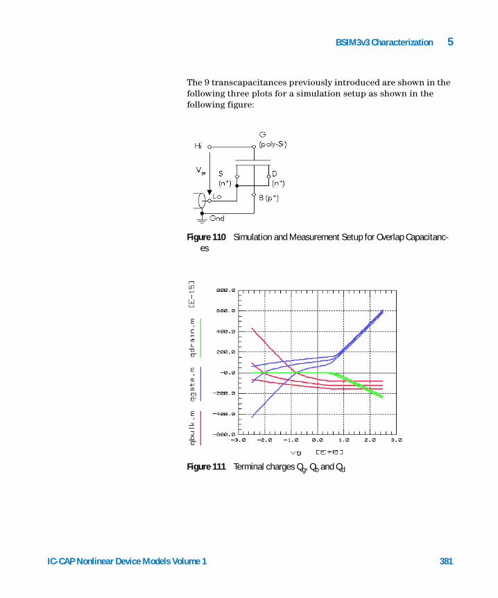
BSIM3v3 Characterization 5
IC-CAP Nonlinear Device Models Vo
The 9 transcapacitances previously introduced are shown in the following three plots for a simulation setup as shown in the following figure:
Figure 110 Simulation and Measurement Setup for Overlap Capacitanc-es
Figure 111 Terminal charges Qg, Qb and Qd
lume 1 381
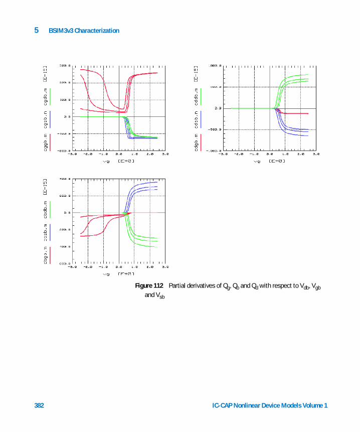
382
5 BSIM3v3 Characterization
Figure 112 Partial derivatives of Qg, Qb and Qd with respect to Vdb, Vgb
and Vsb
IC-CAP Nonlinear Device Models Volume 1
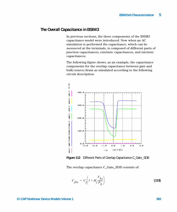
BSIM3v3 Characterization 5
The Overall Capacitance in BSIM3
IC-CAP Nonlinear Device Models Vo
In previous sections, the three components of the BSIM3 capacitance model were introduced. Now when an AC simulation is performed the capacitance, which can be measured at the terminals, is composed of different parts of junction capacitances, extrinsic capacitances, and intrinsic capacitances.
The following figure shows, as an example, the capacitance components for the overlap capacitance between gate and bulk/source/drain as simulated according to the following circuit description:
The overlap capacitance C_Gate_SDB consists of:
(113)
Figure 113 Different Parts of Overlap Capacitance C_Gate_SDB
Cjbs Cj 1 Mj
VbsPb---------+
=
lume 1 383
384
5 BSIM3v3 Characterization
where:
Other capacitances can be calculated in the same way. Please refer to the BSIM3 manual for more details.
Cggb intrinsic capacitance
Cgd,overlap overlap capacitance between gate and drain
Cgs,overlap overlap capacitance between gate and source
Cgb,overlap overlap capacitance between gate and bulk
IC-CAP Nonlinear Device Models Volume 1
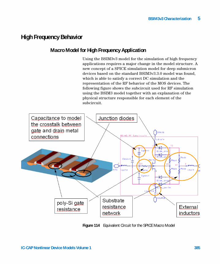
BSIM3v3 Characterization 5
High Frequency Behavior
Macro Model for High Frequency Application
IC-CAP Nonlinear Device Models Vo
Using the BSIM3v3 model for the simulation of high frequency applications requires a major change in the model structure. A new concept of a SPICE simulation model for deep submicron devices based on the standard BSIM3v3.3.0 model was found, which is able to satisfy a correct DC simulation and the representation of the RF behavior of the MOS devices. The following figure shows the subcircuit used for RF simulation using the BSIM3 model together with an explanation of the physical structure responsible for each element of the subcircuit.
Figure 114 Equivalent Circuit for the SPICE Macro Model
lume 1 385

386
5 BSIM3v3 Characterization
The model itself is implemented as the macro model shown above—no changes are done in the BSIM3v3.3.0 model code itself. This is the ultimate precondition for its use in a commercial circuit simulator that includes the BSIM3v3.3.0 model and makes it available to circuit design engineers. The BSIM3v3.3.0 model already consists of a non-quasi-static model and an accurate capacitance model, which makes it the ideal base for RF simulations. However, the description of the resistance behavior of a transistor is very poor. In the BSIM3v3.3.0 model itself, no gate resistance is included. Due to the nature of the MOS transistor, such a resistance cannot be seen in the DC operation region. However, looking at the real existing poly silicon gates of modern MOS devices, there is a resistance which cannot be neglected in AC simulations. This resistance, Rgate, has a major influence on the reflection coefficient S11 of an input signal to the MOS transistor as demonstrated in the following figure.
It should be noted that the parameter Rgate in this high frequency model is used to fit the input reflection of the MOS transistor. Therefore, it is very likely that Rgate has a different value as the measured sheet resistance of the poly-Si gate during process characterization on PCMs using for instance a van-der-Pauw test structure.
The second enhancement in the RF BSIM3v3.3.0 macro model is a resistance network for the substrate resistance, which is described by four resistors RBPD, RBPS, RBDB, and RBSB [7, 8]. The substrate resistance can be seen in the reverse-reflection coefficient S22 at the output of the transistor. Together with the resistance network, the internal drain-bulk and source-bulk junction diodes of the BSIM3v3.3.0 model are replaced by the external elements Djdb_area, Djdb_perim, Djsb_area, and Djsb_perim. The decoupling diodes account for the same voltage dependant values of the bottom and the sidewall capacity as the internal junction capacitances. This replacement is the prerequisite for a correct modeling of the substrate resistance.
With this approach, the model is valid for both the DC and the RF behavior of the transistor.
IC-CAP Nonlinear Device Models Volume 1
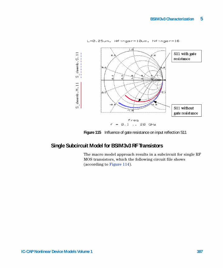
BSIM3v3 Characterization 5
IC-CAP Nonlinear Device Models Vo
Figure 115 Influence of gate resistance on input reflection S11
Single Subcircuit Model for BSIM3v3 RF Transistors
The macro model approach results in a subcircuit for single RF MOS transistors, which the following circuit file shows (according to Figure 114).
lume 1 387

388
5 BSIM3v3 Characterization
Following is part of the SPICE netlist used for single transistors in BSIM3v3 RF modeling.
Figure 116 Subcircuit for RF modeling of single transistors using the BSIM3-model
IC-CAP Nonlinear Device Models Volume 1

BSIM3v3 Characterization 5
LINK CIRC Circuitdatacircuitdeck .OPTIONS GMIN=1.0E-14 * ----------------------------------------------------------------------------- * Single subcircuit model for BSIM3v3.3.0 RF n-type devices * * Simulator: UCB Spice3e2 * Model: BSIM3 Modeling Package * Date: 25.04.2003 * Origin: ICCAP_ROOT/..../bsim3/code/circuits/spice3/cir/rf_nmos_single.cir * ----------------------------------------------------------------------------- * .subckt bsim3_rf_extract 1 2 3 4 * *--- BSIM3 model card ---------------------------------------------------------#echo .MODEL BSIM3_HF NMOS #echo + LEVEL=$mpar(LEVEL=8) VERSION=3.2.4 BINUNIT=$mpar(BINUNIT=2)#echo + MOBMOD=$mpar(MOBMOD=1 CAPMOD=$mpar(CAPMOD=3) NOIMOD=$mpar(NOIMOD=1) #echo + PARAMCHK=$mpar(PARAMCHK=1)#echo + DELTA=$mpar(DELTA=0.01)TNOM=$mpar(TNOM=27)TOX=$mpar(TOX=7.5E-9) #echo + TOXM=$mpar(TOXM=7.5E-9)#echo + NCH =$mpar(NCH=1.7e17) XJ=$mpar(XJ=1.5E-7) NGATE=$mpar(NGATE=0) RSH =$mpar(RSH=0)#echo + VTH0=$mpar(VTH0=0.7) K1=$mpar(K1=0.53) K2=$mpar(K2=-0.013) K3=$mpar(K3=0)#echo + K3B =$mpar(K3B=0) W0=$mpar(W0=2.5E-6) NLX =$mpar(NLX=0.174u) DVT0=$mpar(DVT0=2.2)#echo + DVT1=$mpar(DVT1=0.53) DVT2=$mpar(DVT2=-0.032) DVT0W=$mpar(DVT0W=0) #echo + DVT1W=$mpar(DVT1W=5.3E6)#echo + DVT2W=$mpar(DVT2W=-0.032) ETA0=$mpar(ETA0=0) ETAB=$mpar(ETAB=0) #echo + DSUB=$mpar(DSUB=0.56)#echo + U0=$mpar(U0=670) UA=$mpar(UA=2.25E-9) UB=$mpar(UB=5.87E-19) UC=$mpar(UC=4.65E-11)#echo + VSAT=$mpar(VSAT=8e4) A0=$mpar(A0=1) AGS =$mpar(AGS=0) B0=$mpar(B0=0)#echo + B1=$mpar(B1=0) KETA=$mpar(KETA=-0.047) A1=$mpar(A1=0) A2=$mpar(A2=1)#echo + RDSW=$mpar(RDSW=0) PRWB=$mpar(PRWB=0) PRWG=$mpar(PRWG=0) WR=$mpar(WR=1)#echo + WINT=$mpar(WINT=0) WL=$mpar(WL=0) WLN =$mpar(WLN=1) WW=$mpar(WW=0)#echo + WWN =$mpar(WWN=1) WWL =$mpar(WWL=0) DWG =$mpar(DWG=0) DWB =$mpar(DWB=0)#echo + LINT=$mpar(LINT=0) LL=$mpar(LL=0) LLN =$mpar(LLN=1) LW=$mpar(LW=0)#echo + LWN =$mpar(LWN=1) LWL =$mpar(LWL=0)#echo + VOFF=$mpar(VOFF=-0.08) NFACTOR=$mpar(NFACTOR=1) CIT =$mpar(CIT=0) #echo + CDSC=$mpar(CDSC=2.4E-4)#echo + CDSCB=$mpar(CDSCB=0) CDSCD=$mpar(CDSCD=0) PCLM=$mpar(PCLM=1.3) #echo + PDIBLC1=$mpar(PDIBLC1=0.39)#echo + PDIBLC2=$mpar(PDIBLC2=0.0086) PDIBLCB=$mpar(PDIBLCB=0.0) DROUT=$mpar(DROUT=0.56) #echo + PSCBE1=$mpar(PSCBE1=4.24E8)#echo + PSCBE2=$mpar(PSCBE2=1.0E-5) PVAG=$mpar(PVAG=0) VBM =$mpar(VBM=-3) #echo + ALPHA0=$mpar(ALPHA0=0) ALPHA1=$mpar(ALPHA1=0) BETA0=$mpar(BETA0=30)#echo + JS=1e-20 JSW =1.0E-20 NJ=1 IJTH=$mpar(IJTH=0.1)#echo + CJ=0 MJ=0.5 PB=1 CJSW=0#echo + MJSW=0.33 PBSW=1 CJSWG=$mpar(CJSWG=5E-10) MJSWG=$mpar(MJSWG=0.33)#echo + PBSWG=$mpar(PBSWG=1) CGDO=$mpar(CGDO=0) CGSO=$mpar(CGSO=0) #echo +CGBO=$mpar(CGBO=0)
IC-CAP Nonlinear Device Models Volume 1 389
5 BSIM3v3 Characterization
#echo +CGBO=$mpar(CGBO=0) CGSL=$mpar(CGSL=0) CGDL=$mpar(CGDL=0)#echo + CKAPPA=$mpar(CKAPPA=0.6) CF=$mpar(CF=0)#echo + NOFF=$mpar(NOFF=1) VOFFCV=$mpar(VOFFCV=0) ACDE=$mpar(ACDE=1) #echo + MOIN=$mpar(MOIN=15) DLC=$mpar(DLC=0) DWC=$mpar(DWC=0)#echo + LLC=$mpar(LLC=0) LWC=$mpar(LWC=0) LWLC=$mpar(LWLC=0)#echo + WLC=$mpar(WLC=0) WWC=$mpar(WWC=0) WWLC=$mpar(WWLC=0)#echo + CLC=$mpar(CLC=0.1E-6) CLE=$mpar(CLE=0.6) ELM=$mpar(ELM=2)#echo + XPART=$mpar(XPART=0.5) KT1=$mpar(KT1=-0.11) KT1L=$mpar(KT1L=0)#echo + KT2=$mpar(KT2=0.022) UTE=$mpar(UTE=-1.5) UA1=$mpar(UA1=4.31E-9)#echo + UB1=$mpar(UB1=-7.6E-18) UC1=$mpar(UC1=-5.6E-11) AT=$mpar(AT=3.3E4)#echo + PRT=$mpar(PRT=0) XTI=$mpar(XTI=3.0) TPB=$mpar(TPB=0) #echo + TPBSW=$mpar(TPBSW=0) TPBSWG=$mpar(TPBSWG=0) #echo + TCJ=$mpar(TCJ=0) TCJSW=$mpar(TCJSW=0) TCJSWG=$mpar(TCJSWG=0) #echo + AF=$mpar(AF=1.5) EF=$mpar(EF=1.5) KF=$mpar(KF=1e-17) EM=$mpar(EM=4.1E7)#echo + NOIA=$mpar(NOIA=2e29) NOIB=$mpar(NOIB=5e4) NOIC=$mpar(NOIC=-1.4e-12)*--- Parasitic diode model cards ----------------------------------------------#echo .MODEL bsim_diode_area D #echo + CJO=$mpar(CJ=5E-4) VJ=$mpar(PB=1) M=$mpar(MJ=0.5)#echo + IS=$mpar(JS=1.0E-4) N=$mpar(NJ=1) #echo .MODEL bsim_diode_perim D CJO=$mpar(CJSW=5E-10) VJ=$mpar(PBSW=1)#echo + M=$mpar(MJSW=0.33) IS=$mpar(JSW=1.0E-12) N=$dpar(CALC.NJSW=1) * --------- Gate network ------------------------------------------------------CGDEXT 20 10 0.1fCGSEXT 20 30 0.1fRGATE 20 21 100 LGATE 2 20 1p* --------- Drain network -----------------------------------------------------CDSEXT 10 30 0.1fLDRAIN 1 10 1p* --------- Source network ----------------------------------------------------LSOURCE 3 30 1p * --------- Substrate network -------------------------------------------------* Diodes are for n-type MOS transistors#echo Djdb_area 12 10 bsim_diode_area AREA=$dpar(x_rf_transistor.AD=10e-12)#echo Djdb_perim 12 10 bsim_diode_perim AREA=$dpar(x_rf_transistor.PD=22e-6)#echo Djsb_area 32 30 bsim_diode_area AREA=$dpar(x_rf_transistor.AS=10e-12)#echo Djsb_perim 32 30 bsim_diode_perim AREA=$dpar(x_rf_transistor.PS=22e-6)RBDB 12 40 100RBSB 32 40 100RBPD 12 41 100RBPS 32 41 100LBULK 4 40 1p*--- call single MOSFET -------------------------------------------------------#echo MAIN 10 21 30 41 BSIM3_HF #echo + L=$dpar(x_rf_transistor.L=1u) W=$dpar(x_rf_transistor.W=10e-6) #echo + AD=$dpar(x_rf_transistor.AD=10e-12) AS=$dpar(x_rf_transistor.AS=10e-12) #echo + PD=$dpar(x_rf_transistor.PD=22e-6) PS=$dpar(x_rf_transistor.PS=22e-6) #echo + NRS=$dpar(x_rf_transistor.NRS=0) NRD=$dpar(x_rf_transistor.NRD=0)#echo + NQSMOD=$mpar(NQSMOD=0).ends
390 IC-CAP Nonlinear Device Models Volume 1
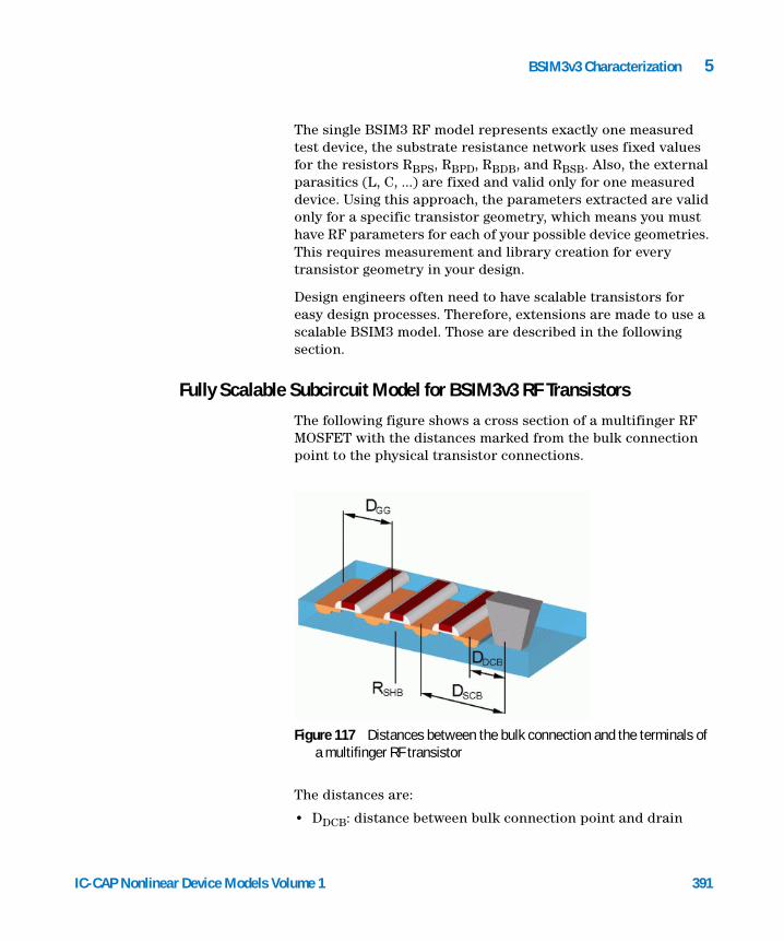
BSIM3v3 Characterization 5
IC-CAP Nonlinear Device Models Vo
The single BSIM3 RF model represents exactly one measured test device, the substrate resistance network uses fixed values for the resistors RBPS, RBPD, RBDB, and RBSB. Also, the external parasitics (L, C, ...) are fixed and valid only for one measured device. Using this approach, the parameters extracted are valid only for a specific transistor geometry, which means you must have RF parameters for each of your possible device geometries. This requires measurement and library creation for every transistor geometry in your design.
Design engineers often need to have scalable transistors for easy design processes. Therefore, extensions are made to use a scalable BSIM3 model. Those are described in the following section.
Fully Scalable Subcircuit Model for BSIM3v3 RF Transistors
The following figure shows a cross section of a multifinger RF MOSFET with the distances marked from the bulk connection point to the physical transistor connections.
The distances are:
• DDCB: distance between bulk connection point and drain
Figure 117 Distances between the bulk connection and the terminals of a multifinger RF transistor
lume 1 391

392
5 BSIM3v3 Characterization
• DDCS: distance between bulk connection point and source
• DGG: distance between gate stripes
Additionally, the sheet resistance of the bulk connection, RSHB, is needed.
Implementations according to “MOS Transistor Modeling for RF IC Design” [8] and our own findings to model a scalable substrate resistance behavior are leading to the following equations, which are implemented into the SPICE subcircuit for the fully scalable BSIM3 RF model.
Using the distances according to the previous figure, the resistors are calculated from:
factor-even-odd = 0.5 for even number of fingers (NF)
factor-even-odd = 1 for odd number of fingers (NF)
The values of the elements of the SPICE equivalent circuit are calculated from device dimensions of the actual device (W, L, NF...) and additional model parameters like the gate sheet resistance RSHG.
Following is a SPICE netlist for the fully scalable BSIM3 model.
RBPS RBPDRSHB L Dgg+( )⋅
2 W⋅------------------------------------------= =
RBSBfactor even– odd–( ) NF DSCB RSHB⋅ ⋅ ⋅
W-------------------------------------------------------------------------------------------------------=
RBDBfactor even– odd–( ) NF DDCB RSHB⋅ ⋅ ⋅
W--------------------------------------------------------------------------------------------------------=
IC-CAP Nonlinear Device Models Volume 1
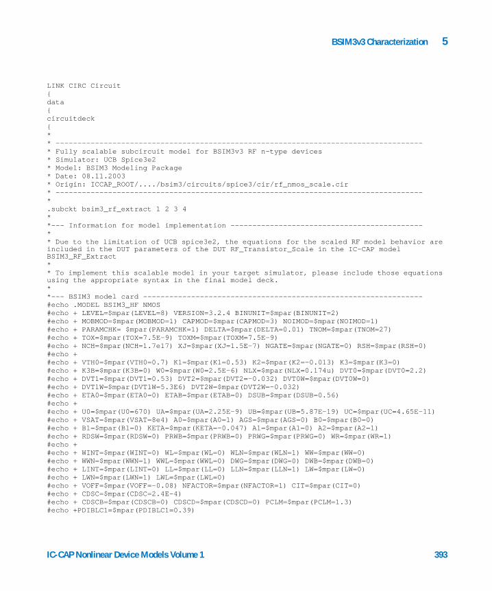
BSIM3v3 Characterization 5
LINK CIRC Circuitdatacircuitdeck* * ------------------------------------------------------------------------------------* Fully scalable subcircuit model for BSIM3v3 RF n-type devices * Simulator: UCB Spice3e2 * Model: BSIM3 Modeling Package * Date: 08.11.2003 * Origin: ICCAP_ROOT/..../bsim3/circuits/spice3/cir/rf_nmos_scale.cir * ------------------------------------------------------------------------------------* .subckt bsim3_rf_extract 1 2 3 4**--- Information for model implementation --------------------------------------------* * Due to the limitation of UCB spice3e2, the equations for the scaled RF model behavior are included in the DUT parameters of the DUT RF_Transistor_Scale in the IC-CAP model BSIM3_RF_Extract** To implement this scalable model in your target simulator, please include those equations using the appropriate syntax in the final model deck.**--- BSIM3 model card ----------------------------------------------------------------#echo .MODEL BSIM3_HF NMOS #echo + LEVEL=$mpar(LEVEL=8) VERSION=3.2.4 BINUNIT=$mpar(BINUNIT=2) #echo + MOBMOD=$mpar(MOBMOD=1) CAPMOD=$mpar(CAPMOD=3) NOIMOD=$mpar(NOIMOD=1) #echo + PARAMCHK= $mpar(PARAMCHK=1) DELTA=$mpar(DELTA=0.01) TNOM=$mpar(TNOM=27)#echo + TOX=$mpar(TOX=7.5E-9) TOXM=$mpar(TOXM=7.5E-9)#echo + NCH=$mpar(NCH=1.7e17) XJ=$mpar(XJ=1.5E-7) NGATE=$mpar(NGATE=0) RSH=$mpar(RSH=0)#echo +#echo + VTH0=$mpar(VTH0=0.7) K1=$mpar(K1=0.53) K2=$mpar(K2=-0.013) K3=$mpar(K3=0)#echo + K3B=$mpar(K3B=0) W0=$mpar(W0=2.5E-6) NLX=$mpar(NLX=0.174u) DVT0=$mpar(DVT0=2.2)#echo + DVT1=$mpar(DVT1=0.53) DVT2=$mpar(DVT2=-0.032) DVT0W=$mpar(DVT0W=0)#echo + DVT1W=$mpar(DVT1W=5.3E6) DVT2W=$mpar(DVT2W=-0.032)#echo + ETA0=$mpar(ETA0=0) ETAB=$mpar(ETAB=0) DSUB=$mpar(DSUB=0.56)#echo +#echo + U0=$mpar(U0=670) UA=$mpar(UA=2.25E-9) UB=$mpar(UB=5.87E-19) UC=$mpar(UC=4.65E-11)#echo + VSAT=$mpar(VSAT=8e4) A0=$mpar(A0=1) AGS=$mpar(AGS=0) B0=$mpar(B0=0)#echo + B1=$mpar(B1=0) KETA=$mpar(KETA=-0.047) A1=$mpar(A1=0) A2=$mpar(A2=1)#echo + RDSW=$mpar(RDSW=0) PRWB=$mpar(PRWB=0) PRWG=$mpar(PRWG=0) WR=$mpar(WR=1)#echo +#echo + WINT=$mpar(WINT=0) WL=$mpar(WL=0) WLN=$mpar(WLN=1) WW=$mpar(WW=0)#echo + WWN=$mpar(WWN=1) WWL=$mpar(WWL=0) DWG=$mpar(DWG=0) DWB=$mpar(DWB=0)#echo + LINT=$mpar(LINT=0) LL=$mpar(LL=0) LLN=$mpar(LLN=1) LW=$mpar(LW=0)#echo + LWN=$mpar(LWN=1) LWL=$mpar(LWL=0)#echo + VOFF=$mpar(VOFF=-0.08) NFACTOR=$mpar(NFACTOR=1) CIT=$mpar(CIT=0)#echo + CDSC=$mpar(CDSC=2.4E-4)#echo + CDSCB=$mpar(CDSCB=0) CDSCD=$mpar(CDSCD=0) PCLM=$mpar(PCLM=1.3) #echo +PDIBLC1=$mpar(PDIBLC1=0.39)
IC-CAP Nonlinear Device Models Volume 1 393
394
5 BSIM3v3 Characterization
0.0086) PDIBLCB=$mpar(PDIBLCB=0.0) DROUT=$mpar(DROUT=0.56)
#echo + PDIBLC2=$mpar(PDIBLC2=#echo + PSCBE1=$mpar(PSCBE1=4.24E8)#echo + PSCBE2=$mpar(PSCBE2=1.0E-5) PVAG=$mpar(PVAG=0) VBM=$mpar(VBM=-3) #echo + ALPHA0=$mpar(ALPHA0=0) ALPHA1=$mpar(ALPHA1=0) BETA0=$mpar(BETA0=30)#echo +#echo + JS=1e-20 JSW=1.0E-20 NJ=1 IJTH=$mpar(IJTH=0.1)#echo +#echo + CJ=0 MJ=0.5 PB=1 CJSW=0#echo + MJSW=0.33 PBSW=1 CJSWG=$mpar(CJSWG=5E-10) MJSWG=$mpar(MJSWG=0.33)#echo + PBSWG=$mpar(PBSWG=1) CGDO=$mpar(CGDO=0) CGSO=$mpar(CGSO=0) CGBO=$mpar(CGBO=0)#echo + CGSL=$mpar(CGSL=0) CGDL=$mpar(CGDL=0) CKAPPA=$mpar(CKAPPA=0.6) CF=$mpar(CF=0)#echo + NOFF=$mpar(NOFF=1) VOFFCV=$mpar(VOFFCV=0) ACDE=$mpar(ACDE=1) MOIN=$mpar(MOIN=15)#echo + DLC=$mpar(DLC=0) DWC=$mpar(DWC=0) LLC=$mpar(LLC=0) LWC=$mpar(LWC=0)#echo + LWLC=$mpar(LWLC=0) WLC=$mpar(WLC=0) WWC=$mpar(WWC=0) WWLC=$mpar(WWLC=0)#echo + CLC=$mpar(CLC=0.1E-6) CLE=$mpar(CLE=0.6)#echo + ELM=$mpar(ELM=2) XPART=$mpar(XPART=0.5)#echo +#echo + KT1=$mpar(KT1=-0.11) KT1L=$mpar(KT1L=0) KT2=$mpar(KT2=0.022) UTE=$mpar(UTE=-1.5)#echo + UA1=$mpar(UA1=4.31E-9) UB1=$mpar(UB1=-7.6E-18) UC1=$mpar(UC1=-5.6E-11)#echo + AT=$mpar(AT=3.3E4)#echo + PRT=$mpar(PRT=0) XTI=$mpar(XTI=3.0) TPB=$mpar(TPB=0) TPBSW=$mpar(TPBSW=0)#echo + TPBSWG=$mpar(TPBSWG=0) TCJ=$mpar(TCJ=0) TCJSW=$mpar(TCJSW=0) TCJSWG=$mpar(TCJSWG=0)#echo +#echo + AF=$mpar(AF=1.5) EF=$mpar(EF=1.5) KF=$mpar(KF=1e-17) EM=$mpar(EM=4.1E7)#echo + NOIA=$mpar(NOIA=2e29) NOIB=$mpar(NOIB=5e4) NOIC=$mpar(NOIC=-1.4e-12)** *--- Parasitic diode model cards ----------------------------------------------------#echo .MODEL bsim_diode_area D #echo + CJO=$mpar(CJ=5E-4) VJ=$mpar(PB=1) M=$mpar(MJ=0.5)#echo + IS=$mpar(JS=1.0E-4) N=$mpar(NJ=1) *#echo .MODEL bsim_diode_perim D #echo + CJO=$mpar(CJSW=5E-10) VJ=$mpar(PBSW=1) M=$mpar(MJSW=0.33)#echo + IS=$mpar(JSW=1.0E-12) N=$dpar(CALC.NJSW=1) ***--- Additional model parameters necessary for scalability---------------------------* - scalable external capacitors and inductors to account for cross coupling in the metal stripes and additional delay due to large sizes* - a scalable substrate network * - a scalable channel length reduction* #echo * CGDEXT0=$mpar(CGDEXT0=1e-9) ext. cap. gate-drain per gate width and finger [F/m]#echo * CGSEXT0=$mpar(CGSEXT0=1e-9) ext. cap. gate-source per gate width and finger [F/m]#echo * CDSEXT0=$mpar(CDSEXT0=1e-9) ext. cap. drain-source per gate width and finger [F/m]#echo * RSHG=$mpar(RSHG=25) gate sheet resistance [Ohm sq]#echo * LDRAIN0=$mpar(LDRAIN0=1e-6) drain inductance per gate width and gate finger [H/m]#echo * LGATE0=$mpar(LGATE0=1e-6) gate inductance per gate width and gate finger [H/m]
IC-CAP Nonlinear Device Models Volume 1
BSIM3v3 Characterization 5
IC-CAP Nonlinear Device Models Vo
#echo * LSOURCE0=$mpar(LSOURCE0=1e-6) source inductance per gate width and finger [H/m]#echo * LBULK0=$mpar(LBULK0=1e-6) bulk inductance per gate width and finger [H/m]#echo * RSHB=$mpar(RSHB=25) bulk sheet resistance [Ohm sq]#echo * DSBC=$mpar(DSBC=2e-6) distance source implant to bulk contact [m]#echo * DDBC=$mpar(DDBC=2e-6) distance drain implant to bulk contact [m]#echo * DGG=$mpar(DGG=2e-6) distance gate to gate [m]#echo * DL0=$mpar(DL0=0) basic channel length reduction correction [m]#echo * DL1=$mpar(DL1=0) channel length reduction correction 1. and 2. outer fingers [m]#echo * DL2=$mpar(DL2=0) channel length reduction correction outer fingers [m]*** --------- Gate network ------------------------------------------------------------#echo LGATE 2 20 $dpar(CALC.LGATE=0.1p)#echo RGATE 20 21 $dpar(CALC.RGATE=10)#echo CGDEXT 20 10 $dpar(CALC.CGDEXT=0.1f)#echo CGSEXT 20 30 $dpar(CALC.CGSEXT=0.1f)** --------- Drain network -----------------------------------------------------------#echo LDRAIN 1 10 $dpar(CALC.LDRAIN=0.1p)#echo CDSEXT 10 30 $dpar(CALC.CDSEXT=0.1f)
* --------- Source network ----------------------------------------------------------#echo LSOURCE 3 30 $dpar(CALC.LSOURCE=0.1p)** --------- Substrate network -------------------------------------------------------* Diodes are for n-type MOS transistors*#echo Djdb_area 12 10 bsim_diode_area AREA=$dpar(x_rf_transistor.AD=10e-12)#echo Djdb_perim 12 10 bsim_diode_perim AREA=$dpar(x_rf_transistor.PD=22e-6)*#echo Djsb_area 32 30 bsim_diode_area AREA=$dpar(x_rf_transistor.AS=10e-12)#echo Djsb_perim 32 30 bsim_diode_perim AREA=$dpar(x_rf_transistor.PS=22e-6)*#echo RBDB 12 40 $dpar(CALC.RBDB=100)#echo RBSB 32 40 $dpar(CALC.RBSB=100)#echo RBPD 12 41 $dpar(CALC.RBPD=100)#echo RBPS 32 41 $dpar(CALC.RBPS=100)*#echo LBULK 4 40 $dpar(CALC.LBULK=0.1p)**--- call single MOSFET -----------------------------------------------------------#echo MAIN 10 21 30 41 BSIM3_HF #echo + L=$dpar(x_rf_transistor.L=1u) W=$dpar(x_rf_transistor.W=10e-6) #echo + AD=$dpar(x_rf_transistor.AD=10e-12) AS=$dpar(x_rf_transistor.AS=10e-12) #echo + PD=$dpar(x_rf_transistor.PD=22e-6) PS=$dpar(x_rf_transistor.PS=22e-6) #echo + NRS=$dpar(x_rf_transistor.NRS=0) NRD=$dpar(x_rf_transistor.NRD=0)#echo + NQSMOD=$mpar(NQSMOD=0)*.ends
lume 1 395
5 BSIM3v3 Characterization
Modeling Strategy
396
Modeling the AC behavior of a MOS device with the BSIM3v3 model heavily depends on the accurate modeling of the DC curves and the capacitances at low frequencies, for example, 10kHz to 1MHz. However, more and more applications, especially in the telecommunication industry, require the modeling of MOS transistors for the use in a frequency range of 1 to 10 GHz. Therefore, S-parameter measurements have to be done (see also “Test Structures for S-parameter Measurements” on page 431) to cover this frequency range by a proper device model.
As is pointed out, using the BSIM3v3 model for high frequency applications requires some special attention to the modeling strategy. We found the following procedure to give the most accurate results:
• Measurement of DC and CV curves.
• Extraction of the BSIM3v3 model parameters from DC and CV measurements with a special emphasis on a physically based extraction strategy. Here, model parameters should not be used for fitting purposes, they should have a correct physical meaning.
• The modeling of the output characteristic Id=f(Vds) and the output resistance Rout=f(Vds) is very important for further S-parameter measurements (see Figure 121 and Figure 120).
• Performing S-parameter measurements and proper de-embedding of parasitics.
• The starting points of the S-parameter curves at the lowest frequency can be modeled by fitting the curves with DC and capacitance parameters. The following diagrams describe this influence on the high frequency behavior.
IC-CAP Nonlinear Device Models Volume 1
BSIM3v3 Characterization 5
IC-CAP Nonlinear Device Models Vo
Figure 118 Incorrectly Modeled Drain Current
Figure 119 Incorrectly Modeled Output Characteristic
lume 1 397
398
5 BSIM3v3 Characterization
• Extraction of the gate resistance from the input reflection S11 (see the following figure)
• Verification of the gate-drain overlap capacitance for higher frequencies
• Extraction of the substrate resistance network parameters from S22 (see the following figure)
• If a good fitting could not be found, additional peripheral elements like inductances at drain, gate, or source should be added in a further sub-circuit
Figure 120 Influence of Incorrectly Modeled Output Characteristic on S21
IC-CAP Nonlinear Device Models Volume 1
BSIM3v3 Characterization 5
IC-CAP Nonlinear Device Models Vo
Figure 121 Input Reflection Parameter S11
Figure 122 Output Reflection Parameter S22
lume 1 399

400
5 BSIM3v3 Characterization
Figure 123 Forward Transmission Parameter S21
Figure 124 Reverse Transmission Parameter S12
IC-CAP Nonlinear Device Models Volume 1

BSIM3v3 Characterization 5
Temperature Dependence
IC-CAP Nonlinear Device Models Vo
Please use the model bsim3_tutor_temp.mdl provided with the BSIM3v3 Modeling Package to visualize the temperature model parameters. Load the file into IC-CAP and run the different macros to see how certain parameters affect the device behavior of a deep submicron MOS transistor.
Built-in Temperature Dependencies
The BSIM3v3 model uses some physically based built-in temperature dependencies as listed below:
Temperature voltage:
(114)
Intrinsic carrier concentration:
(115)
Unfortunately, the surface potential ΦS, which is a very important model parameter from a physical point of view is not temperature dependent in BSIM3.
(116)
VtmkBT
q----------=
Ni 2.631016
T3 2⁄
e
6885T
------------–
=
Φs 2Vtm Tnom( )lnNch
Ni Tnom( )-------------------------
=
Temperature Effects
In addition to the built-in temperature dependencies, the following temperature related effects are modeled in BSIM3. They are related to threshold voltage, mobility, saturation of carrier velocity, drain-source resistance, and the saturation current of the drain/source bulk diodes.
a) Threshold Voltage
lume 1 401
402
5 BSIM3v3 Characterization
(117)
The behavior of the threshold voltage for a large and a short device is shown in tThe following figure.
Figure 125 Threshold Voltage Vth=f(T) of a Large Device
Vth T( ) Vth Tnom( ) KT1
KT1L
Leff-------------- KT2Vbseff+ +
T
Tnom-------------- 1– +=
Vbs = min
Vbs = 0 V
IC-CAP Nonlinear Device Models Volume 1
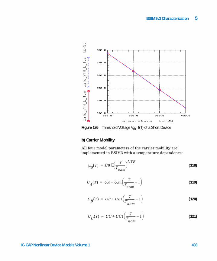
BSIM3v3 Characterization 5
IC-CAP Nonlinear Device Models Vo
b) Carrier Mobility
All four model parameters of the carrier mobility are implemented in BSIM3 with a temperature dependence:
(118)
(119)
(120)
(121)
Figure 126 Threshold Voltage Vth=f(T) of a Short Device
µ0 T( ) U0T
Tnom-------------- ⋅
UTE=
UA T( ) UA UA1T
Tnom-------------- 1– +=
UB T( ) UB UB1T
Tnom-------------- 1– +=
UC T( ) UC UC1T
Tnom-------------- 1– +=
lume 1 403

404
5 BSIM3v3 Characterization
The following two diagrams show the effect of temperature dependent mobility on the transconductance of a large transistor.
Figure 127 Temperature Dependence of Carrier Mobility U0: Influence on Drain Current
UTE = 0
UTE = -1.5
IC-CAP Nonlinear Device Models Volume 1
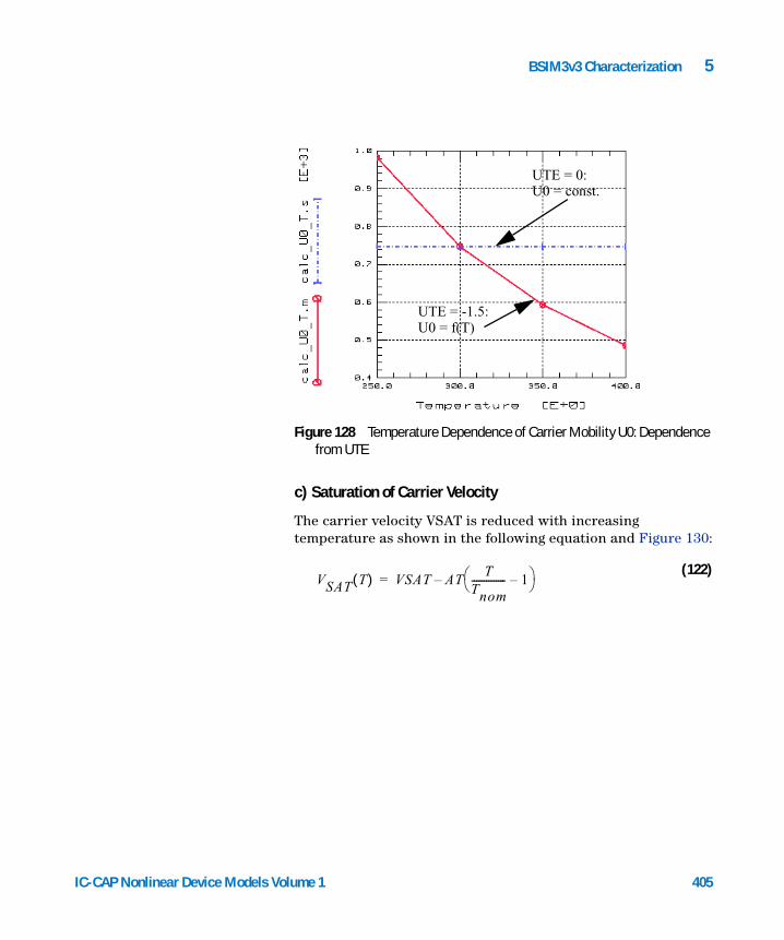
BSIM3v3 Characterization 5
IC-CAP Nonlinear Device Models Vo
c) Saturation of Carrier Velocity
The carrier velocity VSAT is reduced with increasing temperature as shown in the following equation and Figure 130:
(122)
Figure 128 Temperature Dependence of Carrier Mobility U0: Dependence from UTE
UTE = 0:U0 = const.
UTE = -1.5:U0 = f(T)
VSAT T( ) VSAT ATT
Tnom-------------- 1– –=
lume 1 405
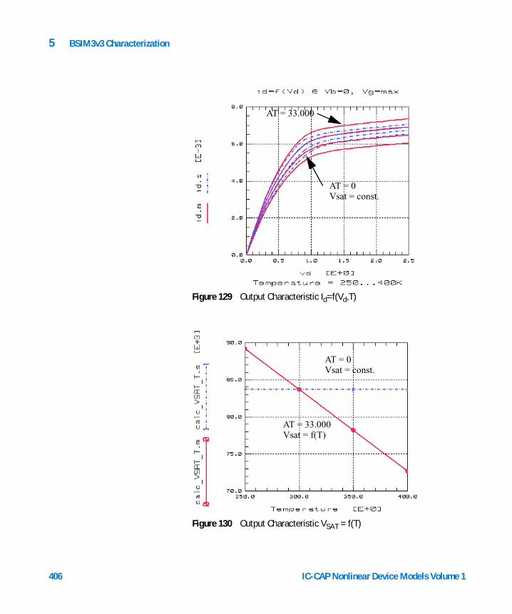
406
5 BSIM3v3 Characterization
Figure 129 Output Characteristic Id=f(Vd,T)
Figure 130 Output Characteristic VSAT = f(T)
AT = 33.000
AT = 0Vsat = const.
AT = 0Vsat = const.
AT = 33.000Vsat = f(T)
IC-CAP Nonlinear Device Models Volume 1
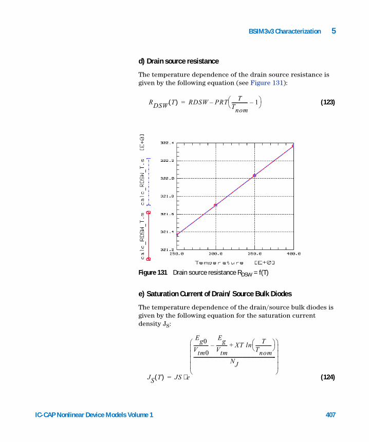
BSIM3v3 Characterization 5
IC-CAP Nonlinear Device Models Vo
d) Drain source resistance
The temperature dependence of the drain source resistance is given by the following equation (see Figure 131):
(123)
e) Saturation Current of Drain/Source Bulk Diodes
The temperature dependence of the drain/source bulk diodes is given by the following equation for the saturation current density JS:
(124)
Figure 131 Drain source resistance RDSW = f(T)
RDSW T( ) RDSW PRTT
Tnom-------------- 1– –=
JS T( ) JS e
Eg0Vtm0-------------
EgVtm----------– XT ln
TTnom-------------- +
NJ------------------------------------------------------------------------
⋅=
lume 1 407
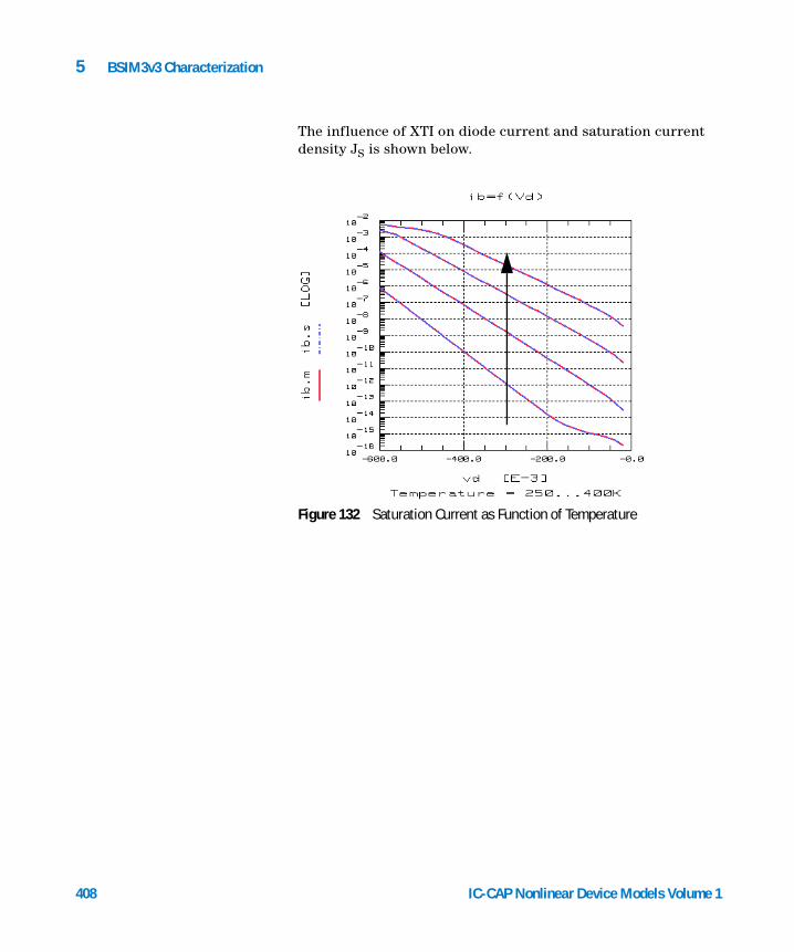
408
5 BSIM3v3 Characterization
The influence of XTI on diode current and saturation current density JS is shown below.
Figure 132 Saturation Current as Function of Temperature
IC-CAP Nonlinear Device Models Volume 1

BSIM3v3 Characterization 5
Noise Model
IC-CAP Nonlinear Device Models Vo
There are two noise models implemented in BSIM3—a conventional noise model named Spice2 model and a newly formulated noise model, which is referred to as BSIM3v3 noise model. The following equations and diagrams should give insight into these two noise formulations.
Please use the model bsim3_tutor_ac_noise.mdl provided with the BSIM3v3 Modeling Package to visualize the model parameters. Load the file into IC-CAP and run the different macros to see how certain parameters affect the device behavior of a deep submicron MOS transistor.
Conventional Noise Model for MOS Devices
Flicker noise:
(125)
Channel thermal noise:
(126)
Vnoise eff,KF1ds
AF
Cox Leff2
fEF×
----------------------------------------=
Vnoise eff,8kT
3--------- gm gds gmb+ +( )=
lume 1 409
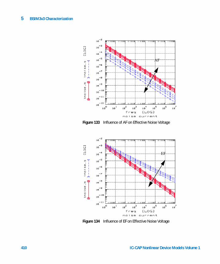
410
5 BSIM3v3 Characterization
Figure 133 Influence of AF on Effective Noise Voltage
Figure 134 Influence of EF on Effective Noise Voltage
AF
EF
IC-CAP Nonlinear Device Models Volume 1

BSIM3v3 Characterization 5
BSIM3v3 Noise Model
IC-CAP Nonlinear Device Models Vo
The BSIM3v3 noise model uses the following equation to describe the flicker noise:
(127)
where:
No is the charge density at the source given by:
(128)
Nl is the charge density at the drain given by:
(129)
The channel thermal noise is given by:
(130)
with:
(131)
Vnoise eff,Vtmq
2ldsµeff
108
CoxLeff2
fEF
-------------------------------------------- NOIA No 2 10× 14
+
Nl 2 10× 14+
----------------------------------- NOIB No Nl–( )+
…+log=
NoCox Vgs Vth–( )
q---------------------------------------=
NlCox Vgs Vth– Vds ′–( )
q---------------------------------------------------------=
Vnoise eff,4kTµeff
Leff2
-------------------- Qinv=
Qinv WeffLeffCoxVgsteff 1Abulk
2 Vgsteff 2Vtm+( )----------------------------------------------Vdseff–
–=
lume 1 411
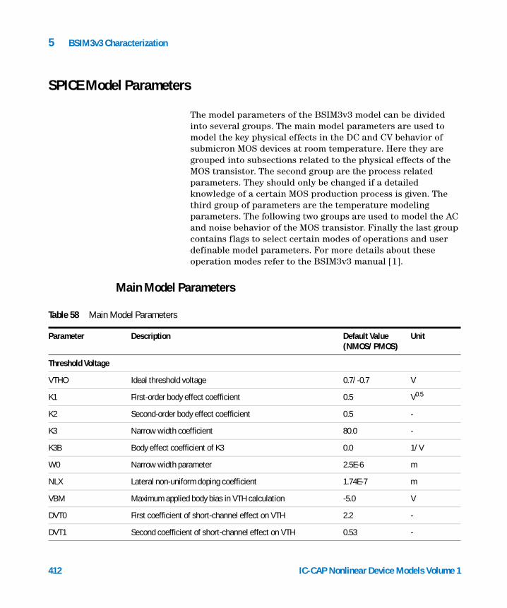
5 BSIM3v3 Characterization
SPICE Model Parameters
412
The model parameters of the BSIM3v3 model can be divided into several groups. The main model parameters are used to model the key physical effects in the DC and CV behavior of submicron MOS devices at room temperature. Here they are grouped into subsections related to the physical effects of the MOS transistor. The second group are the process related parameters. They should only be changed if a detailed knowledge of a certain MOS production process is given. The third group of parameters are the temperature modeling parameters. The following two groups are used to model the AC and noise behavior of the MOS transistor. Finally the last group contains flags to select certain modes of operations and user definable model parameters. For more details about these operation modes refer to the BSIM3v3 manual [1].
Main Model Parameters
Table 58 Main Model Parameters
Parameter Description Default Value(NMOS/PMOS)
Unit
Threshold Voltage
VTHO Ideal threshold voltage 0.7/-0.7 V
K1 First-order body effect coefficient 0.5 V0.5
K2 Second-order body effect coefficient 0.5 -
K3 Narrow width coefficient 80.0 -
K3B Body effect coefficient of K3 0.0 1/V
W0 Narrow width parameter 2.5E-6 m
NLX Lateral non-uniform doping coefficient 1.74E-7 m
VBM Maximum applied body bias in VTH calculation -5.0 V
DVT0 First coefficient of short-channel effect on VTH 2.2 -
DVT1 Second coefficient of short-channel effect on VTH 0.53 -
IC-CAP Nonlinear Device Models Volume 1
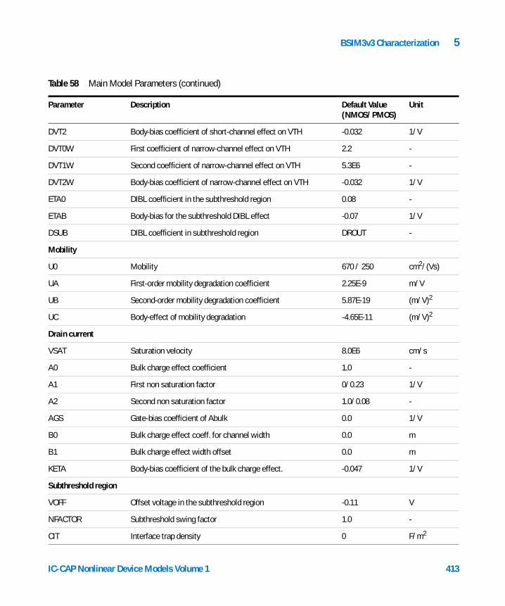
BSIM3v3 Characterization 5
DVT2 Body-bias coefficient of short-channel effect on VTH -0.032 1/V
DVT0W First coefficient of narrow-channel effect on VTH 2.2 -
DVT1W Second coefficient of narrow-channel effect on VTH 5.3E6 -
DVT2W Body-bias coefficient of narrow-channel effect on VTH -0.032 1/V
ETA0 DIBL coefficient in the subthreshold region 0.08 -
ETAB Body-bias for the subthreshold DIBL effect -0.07 1/V
DSUB DIBL coefficient in subthreshold region DROUT -
Mobility
U0 Mobility 670 / 250 cm2/(Vs)
UA First-order mobility degradation coefficient 2.25E-9 m/V
UB Second-order mobility degradation coefficient 5.87E-19 (m/V)2
UC Body-effect of mobility degradation -4.65E-11 (m/V)2
Drain current
VSAT Saturation velocity 8.0E6 cm/s
A0 Bulk charge effect coefficient 1.0 -
A1 First non saturation factor 0/0.23 1/V
A2 Second non saturation factor 1.0/0.08 -
AGS Gate-bias coefficient of Abulk 0.0 1/V
B0 Bulk charge effect coeff. for channel width 0.0 m
B1 Bulk charge effect width offset 0.0 m
KETA Body-bias coefficient of the bulk charge effect. -0.047 1/V
Subthreshold region
VOFF Offset voltage in the subthreshold region -0.11 V
NFACTOR Subthreshold swing factor 1.0 -
CIT Interface trap density 0 F/m2
Table 58 Main Model Parameters (continued)
Parameter Description Default Value(NMOS/PMOS)
Unit
IC-CAP Nonlinear Device Models Volume 1 413
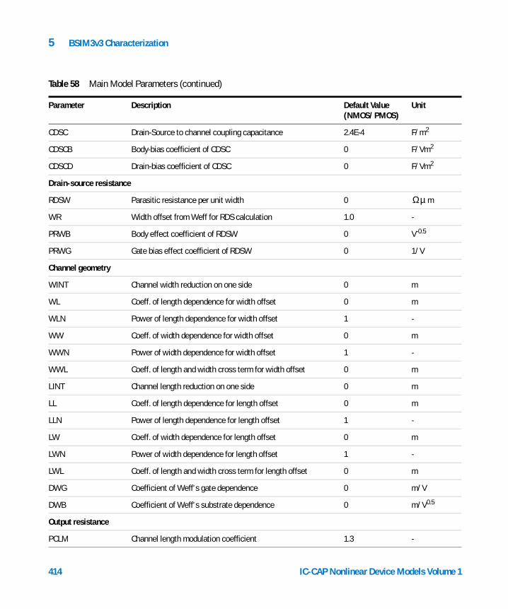
5 BSIM3v3 Characterization
CDSC Drain-Source to channel coupling capacitance 2.4E-4 F/m2
CDSCB Body-bias coefficient of CDSC 0 F/Vm2
CDSCD Drain-bias coefficient of CDSC 0 F/Vm2
Drain-source resistance
RDSW Parasitic resistance per unit width 0 m
WR Width offset from Weff for RDS calculation 1.0 -
PRWB Body effect coefficient of RDSW 0 V-0.5
PRWG Gate bias effect coefficient of RDSW 0 1/V
Channel geometry
WINT Channel width reduction on one side 0 m
WL Coeff. of length dependence for width offset 0 m
WLN Power of length dependence for width offset 1 -
WW Coeff. of width dependence for width offset 0 m
WWN Power of width dependence for width offset 1 -
WWL Coeff. of length and width cross term for width offset 0 m
LINT Channel length reduction on one side 0 m
LL Coeff. of length dependence for length offset 0 m
LLN Power of length dependence for length offset 1 -
LW Coeff. of width dependence for length offset 0 m
LWN Power of width dependence for length offset 1 -
LWL Coeff. of length and width cross term for length offset 0 m
DWG Coefficient of Weff's gate dependence 0 m/V
DWB Coefficient of Weff's substrate dependence 0 m/V0.5
Output resistance
PCLM Channel length modulation coefficient 1.3 -
Table 58 Main Model Parameters (continued)
Parameter Description Default Value(NMOS/PMOS)
Unit
Ωµ
414 IC-CAP Nonlinear Device Models Volume 1
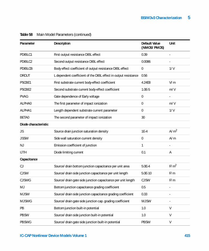
BSIM3v3 Characterization 5
PDIBLC1 First output resistance DIBL effect 0.39 -
PDIBLC2 Second output resistance DIBL effect 0.0086 -
PDIBLCB Body effect coefficient of output resistance DIBL effect 0 1/V
DROUT L dependent coefficient of the DIBL effect in output resistance 0.56
PSCBE1 First substrate current body-effect coefficient 4.24E8 V/m
PSCBE2 Second substrate current body-effect coefficient 1.0E-5 m/V
PVAG Gate dependence of Early voltage 0 -
ALPHA0 The first parameter of impact ionization 0 m/V
ALPHA1 Length dependent substrate current parameter 0 1/V
BETA0 The second parameter of impact ionization 30
Diode characteristic
JS Source drain junction saturation density 1E-4 A/m2
JSSW Side wall saturation current density 0 A/m
NJ Emission coefficient of junction 1 -
IJTH Diode limiting current 0.1 A
Capacitance
CJ Source/drain bottom junction capacitance per unit area 5.0E-4 F/m2
CJSW Source/drain side junction capacitance per unit length 5.0E-10 F/m
CJSWG Source/drain gate side junction capacitance per unit length CJSW F/m
MJ Bottom junction capacitance grading coefficient 0.5 -
MJSW Source/drain side junction capacitance grading coefficient 0.33 -
MJSWG Source/drain gate side junction cap. grading coefficient MJSW -
PB Bottom junction built-in potential 1.0 V
PBSW Source/drain side junction built-in potential 1.0 V
PBSWG Source/drain gate side junction built-in potential PBSW V
Table 58 Main Model Parameters (continued)
Parameter Description Default Value(NMOS/PMOS)
Unit
IC-CAP Nonlinear Device Models Volume 1 415
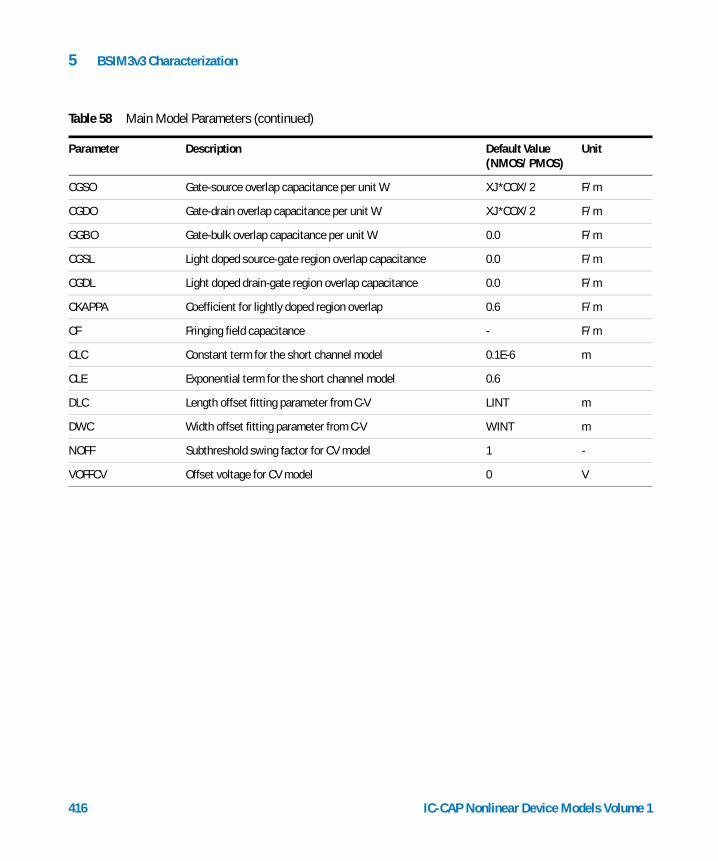
5 BSIM3v3 Characterization
CGSO Gate-source overlap capacitance per unit W XJ*COX/2 F/m
CGDO Gate-drain overlap capacitance per unit W XJ*COX/2 F/m
GGBO Gate-bulk overlap capacitance per unit W 0.0 F/m
CGSL Light doped source-gate region overlap capacitance 0.0 F/m
CGDL Light doped drain-gate region overlap capacitance 0.0 F/m
CKAPPA Coefficient for lightly doped region overlap 0.6 F/m
CF Fringing field capacitance - F/m
CLC Constant term for the short channel model 0.1E-6 m
CLE Exponential term for the short channel model 0.6
DLC Length offset fitting parameter from C-V LINT m
DWC Width offset fitting parameter from C-V WINT m
NOFF Subthreshold swing factor for CV model 1 -
VOFFCV Offset voltage for CV model 0 V
Table 58 Main Model Parameters (continued)
Parameter Description Default Value(NMOS/PMOS)
Unit
416 IC-CAP Nonlinear Device Models Volume 1
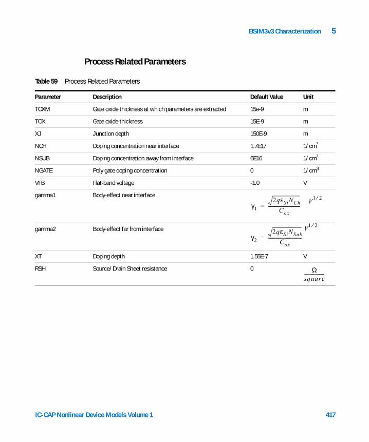
BSIM3v3 Characterization 5
Process Related Parameters
IC-CAP Nonlinear Device Models Vo
rs
Table 59 Process Related Paramete
Parameter Description Default Value Unit
TOXM Gate oxide thickness at which parameters are extracted 15e-9 m
TOX Gate oxide thickness 15E-9 m
XJ Junction depth 150E-9 m
NCH Doping concentration near interface 1.7E17 1/cm³
NSUB Doping concentration away from interface 6E16 1/cm³
NGATE Poly gate doping concentration 0 1/cm3
VFB Flat-band voltage -1.0 V
gamma1 Body-effect near interface
gamma2 Body-effect far from interface
XT Doping depth 1.55E-7 V
RSH Source/Drain Sheet resistance 0
γ1
2qεSiNCh
Cox----------------------------=
V1 2⁄
γ2
2qεSiNSub
Cox------------------------------=
V1 2⁄
Ωsquare------------------
lume 1 417
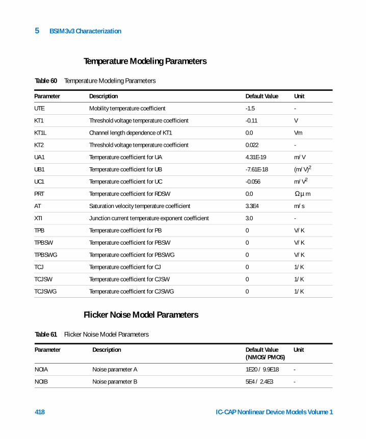
5 BSIM3v3 Characterization
Temperature Modeling Parameters
418
rameters
Flicker Noise Model Parameters
Table 60 Temperature Modeling Pa
Parameter Description Default Value Unit
UTE Mobility temperature coefficient -1.5 -
KT1 Threshold voltage temperature coefficient -0.11 V
KT1L Channel length dependence of KT1 0.0 Vm
KT2 Threshold voltage temperature coefficient 0.022 -
UA1 Temperature coefficient for UA 4.31E-19 m/V
UB1 Temperature coefficient for UB -7.61E-18 (m/V)2
UC1 Temperature coefficient for UC -0.056 m/V2
PRT Temperature coefficient for RDSW 0.0 m
AT Saturation velocity temperature coefficient 3.3E4 m/s
XTI Junction current temperature exponent coefficient 3.0 -
TPB Temperature coefficient for PB 0 V/K
TPBSW Temperature coefficient for PBSW 0 V/K
TPBSWG Temperature coefficient for PBSWG 0 V/K
TCJ Temperature coefficient for CJ 0 1/K
TCJSW Temperature coefficient for CJSW 0 1/K
TCJSWG Temperature coefficient for CJSWG 0 1/K
Ωµ
eters
Table 61 Flicker Noise Model ParamParameter Description Default Value(NMOS/PMOS)
Unit
NOIA Noise parameter A 1E20 / 9.9E18 -
NOIB Noise parameter B 5E4 / 2.4E3 -
IC-CAP Nonlinear Device Models Volume 1
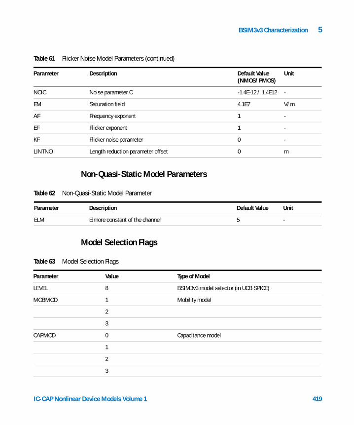
BSIM3v3 Characterization 5
Non-Quasi-Static Model Parameters
NOIC Noise parameter C -1.4E-12 / 1.4E12 -
EM Saturation field 4.1E7 V/m
AF Frequency exponent 1 -
EF Flicker exponent 1 -
KF Flicker noise parameter 0 -
LINTNOI Length reduction parameter offset 0 m
Table 61 Flicker Noise Model Parameters (continued)
Parameter Description Default Value(NMOS/PMOS)
Unit
IC-CAP Nonlinear Device Models Vo
arameter
Model Selection Flags
Table 62 Non-Quasi-Static Model P
Parameter Description Default Value Unit
ELM Elmore constant of the channel 5 -
Table 63 Model Selection Flags
Parameter Value Type of Model
LEVEL 8 BSIM3v3 model selector (in UCB SPICE)
MOBMOD 1 Mobility model
2
3
CAPMOD 0 Capacitance model
1
2
3
lume 1 419
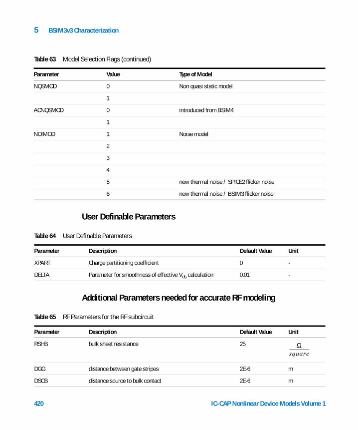
5 BSIM3v3 Characterization
User Definable ParametersNQSMOD 0 Non quasi static model
1
ACNQSMOD 0 introduced from BSIM4
1
NOIMOD 1 Noise model
2
3
4
5 new thermal noise / SPICE2 flicker noise
6 new thermal noise / BSIM3 flicker noise
Table 63 Model Selection Flags (continued)
Parameter Value Type of Model
420
s
Additional Parameters needed for accurate RF modeling
Table 64 User Definable Parameter
Parameter Description Default Value Unit
XPART Charge partitioning coefficient 0 -
DELTA Parameter for smoothness of effective Vds calculation 0.01 -
ubcircuit
Table 65 RF Parameters for the RF sParameter Description Default Value Unit
RSHB bulk sheet resistance 25
DGG distance between gate stripes 2E-6 m
DSCB distance source to bulk contact 2E-6 m
Ωsquare------------------
IC-CAP Nonlinear Device Models Volume 1

BSIM3v3 Characterization 5
DDCB distance drain to bulk contact 2E-6 m
RBDB resistance between bulk connection point and drain 100
RBSB resistance between bulk connection point and source 100
RBPD resistance between the region below the channel and the drain region
100
RBPS resistance between the region below the channel and the source region
100
Table 65 RF Parameters for the RF subcircuit (continued)
Parameter Description Default Value Unit
Ω
Ω
Ω
Ω
IC-CAP Nonlinear Device Models Volume 1 421
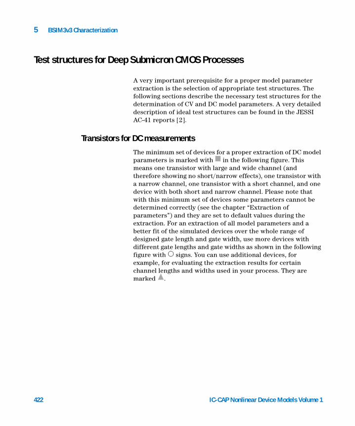
5 BSIM3v3 Characterization
Test structures for Deep Submicron CMOS Processes
422
A very important prerequisite for a proper model parameter extraction is the selection of appropriate test structures. The following sections describe the necessary test structures for the determination of CV and DC model parameters. A very detailed description of ideal test structures can be found in the JESSI AC-41 reports [2].
Transistors for DC measurements
The minimum set of devices for a proper extraction of DC model parameters is marked with in the following figure. This means one transistor with large and wide channel (and therefore showing no short/narrow effects), one transistor with a narrow channel, one transistor with a short channel, and one device with both short and narrow channel. Please note that with this minimum set of devices some parameters cannot be determined correctly (see the chapter “Extraction of parameters”) and they are set to default values during the extraction. For an extraction of all model parameters and a better fit of the simulated devices over the whole range of designed gate length and gate width, use more devices with different gate lengths and gate widths as shown in the following figure with signs. You can use additional devices, for example, for evaluating the extraction results for certain channel lengths and widths used in your process. They are marked .
IC-CAP Nonlinear Device Models Volume 1
BSIM3v3 Characterization 5
IC-CAP Nonlinear Device Models Vo
a) Requirements for Devices
Large For a proper extraction of the basic model parameters, the short and narrow channel effects should not affect the large device extraction. Also the drain-source-resistance parameters should not have an influence on the simulated behavior of the large device. For a typical 0.5 micron CMOS process with a gate oxide thickness of 11 nm, a large device with channel length of 10 microns and channel width of 10 microns was found to meet these requirements.
You can check this prerequisite if you only extract the parameters in the idvg/Large setup and then perform a simulation of the setup idvg/Large_m. After that simulation, perform the other geometry extractions and re-simulate the idvg/Large setup again. Now, the curve ID = f(Vgs) should not change more than roughly 5% compared to the first
Figure 135 Recommended Test Transistor Geometries for proper parame-ter extraction
Design geometries covered by extraction
Design geometries, extrapolated from extraction
Forbidden geometries due to process limitations
lume 1 423
424
5 BSIM3v3 Characterization
simulation. If the difference is bigger, a larger device should be used to enable a good extraction of the basic model parameters.
Narrow For the DUT Narrow_m you should use a device with the smallest designed gate width of your process. Using more narrow devices will increase the number of parameters that can be extracted and will lead to a better fit of the curves over the range of different channel widths.
Short For the DUT Short_m you should use a device with the shortest designed gate length of your process. Using more short devices will increase the number of parameters that can be extracted and will lead to a better fit of the curves over the range of different channel lengths.
Small For the DUT Small_m you should use a device with the shortest designed gate length and the smallest designed gate width of your process. This small device will incorporate all short and narrow channel effects and will be an indicator of how good your parameter extractions are.
In general It is recommended to use the designed gate lengths and widths. Effects due to under diffusion or decrease of poly-Si gate length are sufficiently covered by the extraction routines and the model itself.
IC-CAP Nonlinear Device Models Volume 1
BSIM3v3 Characterization 5
Drain/Source – Bulk Diodes for DC Measurements
IC-CAP Nonlinear Device Models Vo
Source - Bulk Diodes
Test Structures for CV Measurements
Table 66 Test Structures for Drain/
DUT Shape Comment
Diode_Perim_m Finger diode with a large perimeter and a small area (shown here for an n-type device)
Diode_Area_m Area diode with a large area and a small perimeter (shown here for an n-type device)
The following table provides example test structures for measuring capacitance-voltage properties. Each test structure includes a description as well as a schematic for setting up the measurements. You can modify these examples by changing the low and high connection of the CV meter.
lume 1 425
426
5 BSIM3v3 Characterization
asurements
Table 67 Test Structures for CV Me
DUT Shape Applied bias (n-type) Comment
C_Area_m (pn-junction)
Area diode with a large area, a small perimeter and the doping concentration n+ of the drain/source region (shown here for an n-type device).
C_Perim_m (pn-junction)
Finger diode with a large perimeter, a small area and the doping concentration n+ of the drain/source region (shown here for an n-type device).
AD a bPD
⋅2 a b+( )⋅
==
AD NF a bPD
⋅ ⋅NF 2 a b+( )⋅ ⋅
==
IC-CAP Nonlinear Device Models Volume 1
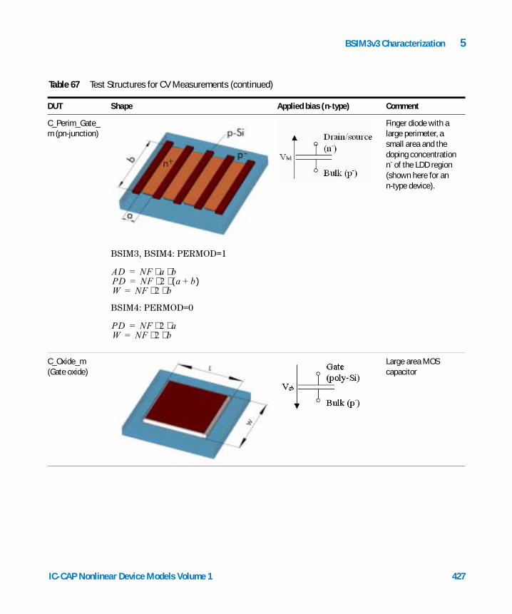
BSIM3v3 Characterization 5
C_Perim_Gate_m (pn-junction)
BSIM3, BSIM4: PERMOD=1
BSIM4: PERMOD=0
Finger diode with a large perimeter, a small area and the doping concentration n- of the LDD region (shown here for an n-type device).
C_Oxide_m (Gate oxide)
Large area MOS capacitor
Table 67 Test Structures for CV Measurements (continued)
DUT Shape Applied bias (n-type) Comment
AD NF a bPD
⋅ ⋅NF 2 a b+( )
W⋅ ⋅
NF 2 b⋅ ⋅
==
=
PD NF 2 aW
⋅ ⋅NF 2 b⋅ ⋅
==
IC-CAP Nonlinear Device Models Volume 1 427
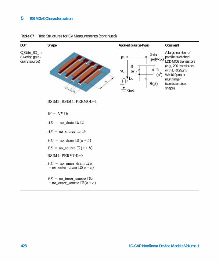
5 BSIM3v3 Characterization
C_Gate_SD_m (Overlap gate - drain/source)
BSIM3, BSIM4: PERMOD=1
BSIM4: PERMOD=0
A large number of parallel switched LDD MOS transistors (e.g., 200 transistors with L=0.25µm, W=10.0µm) or multifinger transistors (see shape)
Table 67 Test Structures for CV Measurements (continued)
DUT Shape Applied bias (n-type) Comment
W NF b⋅=
AD no_drain a b⋅ ⋅=
AS no_source a b⋅ ⋅=
PD no_drain 2 a b+( )⋅=
PS no_source 2 a b+( )⋅=
PD no_inner_drain 2ano_outer_drain 2 a b+( )⋅+
⋅=
PS no_inner_source 2cno_outer_source 2 b c+( )⋅+
⋅=
428 IC-CAP Nonlinear Device Models Volume 1
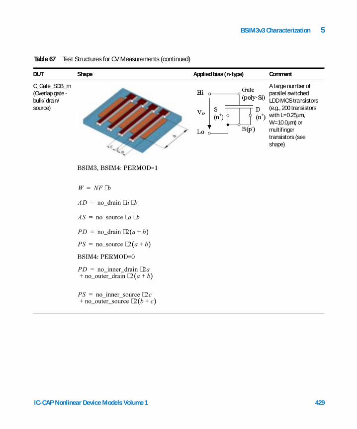
BSIM3v3 Characterization 5
C_Gate_SDB_m (Overlap gate - bulk/drain/ source)
BSIM3, BSIM4: PERMOD=1
BSIM4: PERMOD=0
A large number of parallel switched LDD MOS transistors (e.g., 200 transistors with L=0.25µm, W=10.0µm) or multifinger transistors (see shape)
Table 67 Test Structures for CV Measurements (continued)
DUT Shape Applied bias (n-type) Comment
W NF b⋅=
AD no_drain a b⋅ ⋅=
AS no_source a b⋅ ⋅=
PD no_drain 2 a b+( )⋅=
PS no_source 2 a b+( )⋅=
PD no_inner_drain 2ano_outer_drain 2 a b+( )⋅+
⋅=
PS no_inner_source 2cno_outer_source 2 b c+( )⋅+
⋅=
IC-CAP Nonlinear Device Models Volume 1 429
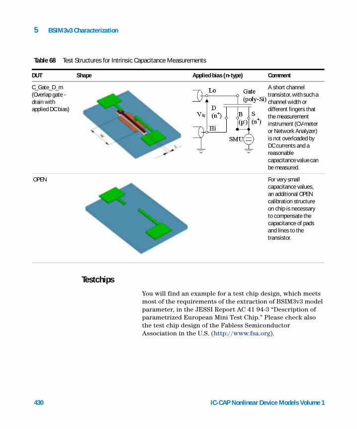
430
5 BSIM3v3 Characterization
c Capacitance Measurements
Testchips
Table 68 Test Structures for Intrinsi
DUT Shape Applied bias (n-type) Comment
C_Gate_D_m (Overlap gate - drain with applied DC bias)
A short channel transistor, with such a channel width or different fingers that the measurement instrument (CV-meter or Network Analyzer) is not overloaded by DC currents and a reasonable capacitance value can be measured.
OPEN For very small capacitance values, an additional OPEN calibration structure on chip is necessary to compensate the capacitance of pads and lines to the transistor.
You will find an example for a test chip design, which meets most of the requirements of the extraction of BSIM3v3 model parameter, in the JESSI Report AC 41 94-3 “Description of parametrized European Mini Test Chip.” Please check also the test chip design of the Fabless Semiconductor Association in the U.S. (http://www.fsa.org).
IC-CAP Nonlinear Device Models Volume 1

BSIM3v3 Characterization 5
Test Structures for S-parameter Measurements
IC-CAP Nonlinear Device Models Vo
a) Test Structures
Performing S-parameter measurements with MOS devices on a wafer requires properly designed test structures that meet certain requirements:
• The test devices must drive enough current for correct measurement results
• They should fulfill the specifications for high frequency probes
• Additional structures should be available for the measurement of parasitic elements to de-embed them from the measurements on the test device
A principle layout of such a test structure is shown in the following figure [9].
lume 1 431
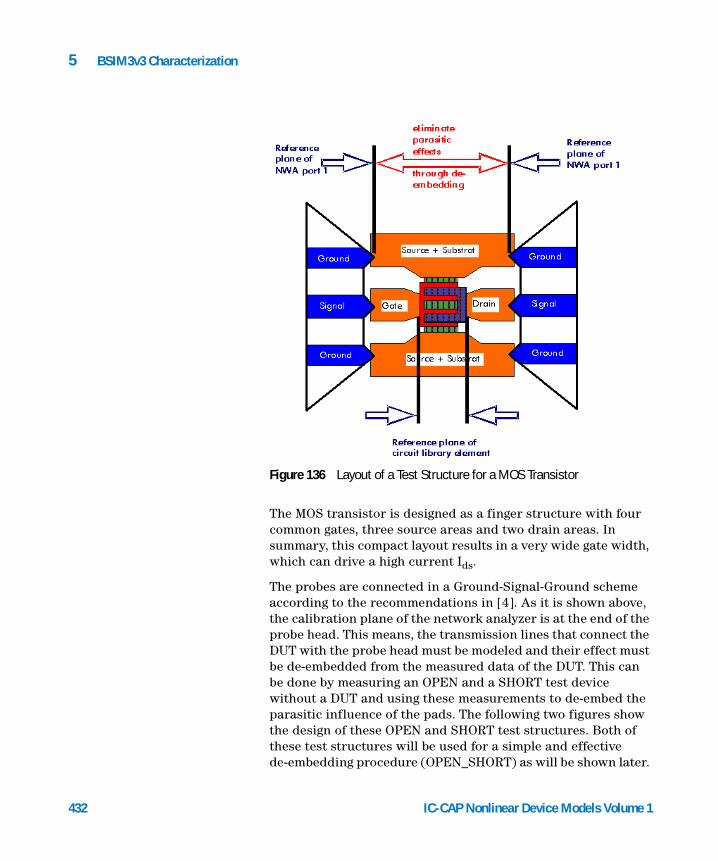
432
5 BSIM3v3 Characterization
The MOS transistor is designed as a finger structure with four common gates, three source areas and two drain areas. In summary, this compact layout results in a very wide gate width, which can drive a high current Ids.
The probes are connected in a Ground-Signal-Ground scheme according to the recommendations in [4]. As it is shown above, the calibration plane of the network analyzer is at the end of the probe head. This means, the transmission lines that connect the DUT with the probe head must be modeled and their effect must be de-embedded from the measured data of the DUT. This can be done by measuring an OPEN and a SHORT test device without a DUT and using these measurements to de-embed the parasitic influence of the pads. The following two figures show the design of these OPEN and SHORT test structures. Both of these test structures will be used for a simple and effective de-embedding procedure (OPEN_SHORT) as will be shown later.
Figure 136 Layout of a Test Structure for a MOS Transistor
IC-CAP Nonlinear Device Models Volume 1

BSIM3v3 Characterization 5
IC-CAP Nonlinear Device Models Vo
Additional test devices, like a THROUGH device can be used to verify the de-embedding strategy. In general, the complexity of the de-embedding procedure depends on the frequency range of the measurements and the design of the test structures. However, a proper de-embedding is the absolute pre-requisite for an accurate AC modeling of the MOS transistor.
Figure 137 OPEN, SHORT and THROUGH structure without MOS transistor
Table 69 Test Structures for S-parameter Measurements
Test Structure Top View Input in ‘___Define DUT
One single transistor
No of gates:No of drains:No of sources:L:W:Area drain:Area source:Per. drain:Per. source:
111LWADASPDPS
W bAD a bPD
⋅2 a b+( )
AS⋅
c bPS
⋅2 b c+( )⋅
=====
lume 1 433
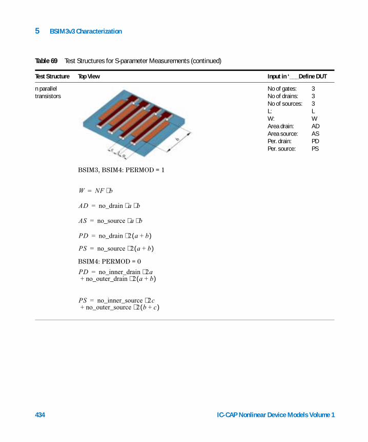
5 BSIM3v3 Characterization
n parallel transistors
BSIM3, BSIM4: PERMOD = 1
BSIM4: PERMOD = 0
No of gates: No of drains: No of sources: L: W: Area drain: Area source: Per. drain: Per. source:
333LWADASPDPS
Table 69 Test Structures for S-parameter Measurements (continued)
Test Structure Top View Input in ‘___Define DUT
W NF b⋅=
AD no_drain a b⋅ ⋅=
AS no_source a b⋅ ⋅=
PD no_drain 2 a b+( )⋅=
PS no_source 2 a b+( )⋅=
PD no_inner_drain 2ano_outer_drain 2 a b+( )⋅+
⋅=
PS no_inner_source 2cno_outer_source 2 b c+( )⋅+
⋅=
434 IC-CAP Nonlinear Device Models Volume 1
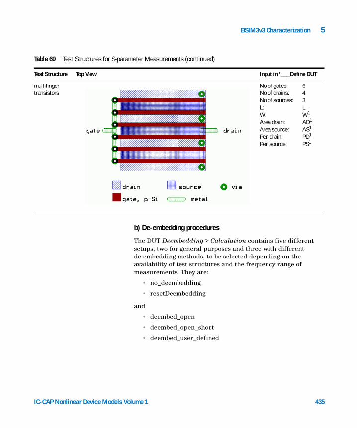
BSIM3v3 Characterization 5
multifinger transistors
No of gates: No of drains: No of sources: L: W: Area drain: Area source: Per. drain: Per. source:
643LW1
AD1
AS1
PD1
PS1
Table 69 Test Structures for S-parameter Measurements (continued)
Test Structure Top View Input in ‘___Define DUT
IC-CAP Nonlinear Device Models Vo
b) De-embedding procedures
The DUT Deembedding > Calculation contains five different setups, two for general purposes and three with different de-embedding methods, to be selected depending on the availability of test structures and the frequency range of measurements. They are:
• no_deembedding
• resetDeembedding
and
• deembed_open
• deembed_open_short
• deembed_user_defined
lume 1 435
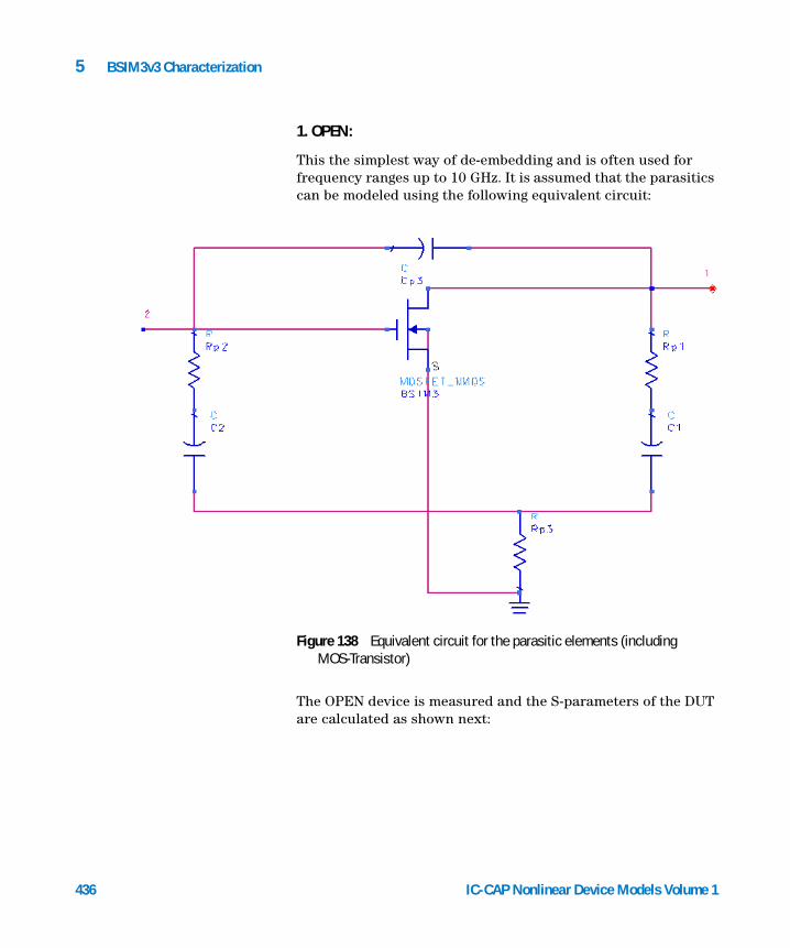
436
5 BSIM3v3 Characterization
1. OPEN:
This the simplest way of de-embedding and is often used for frequency ranges up to 10 GHz. It is assumed that the parasitics can be modeled using the following equivalent circuit:
The OPEN device is measured and the S-parameters of the DUT are calculated as shown next:
Figure 138 Equivalent circuit for the parasitic elements (including MOS-Transistor)
IC-CAP Nonlinear Device Models Volume 1
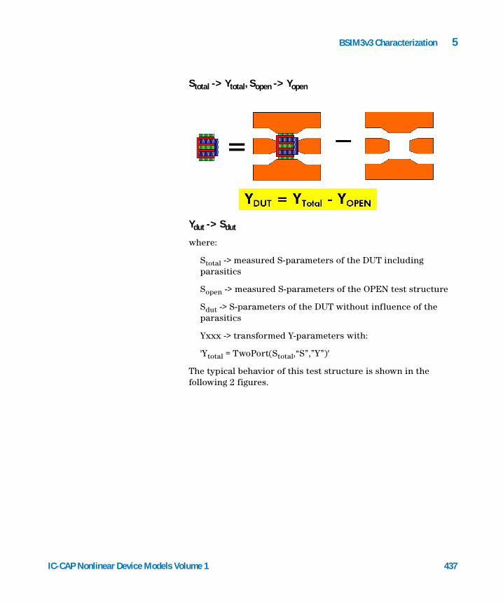
BSIM3v3 Characterization 5
IC-CAP Nonlinear Device Models Vo
Stotal -> Ytotal, Sopen -> Yopen
Ydut -> Sdut
where:
Stotal -> measured S-parameters of the DUT including parasitics
Sopen -> measured S-parameters of the OPEN test structure
Sdut -> S-parameters of the DUT without influence of the parasitics
Yxxx -> transformed Y-parameters with:
'Ytotal = TwoPort(Stotal,“S”,”Y”)'
The typical behavior of this test structure is shown in the following 2 figures.
lume 1 437
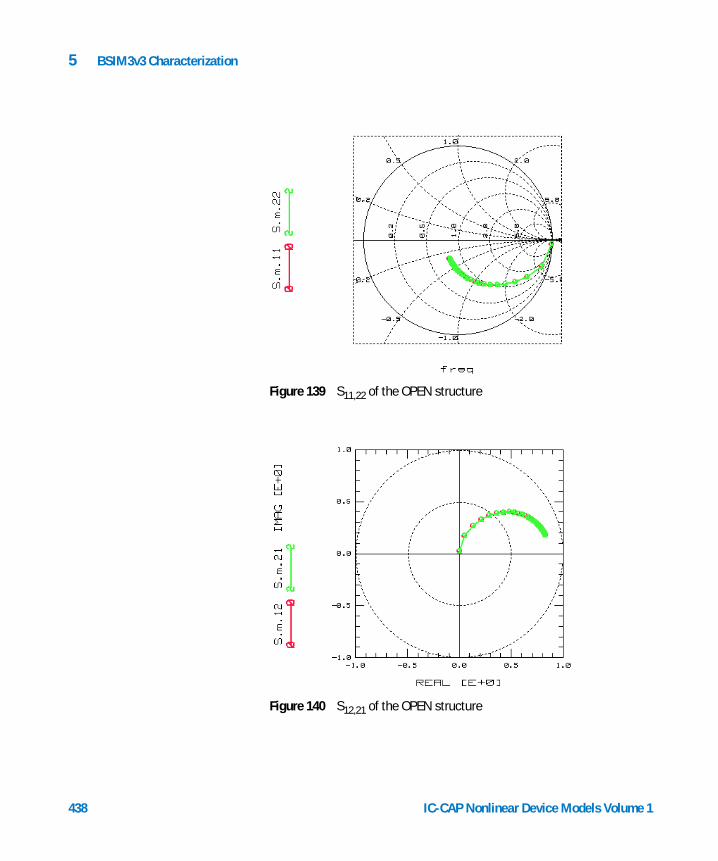
438
5 BSIM3v3 Characterization
Figure 139 S11,22 of the OPEN structure
Figure 140 S12,21 of the OPEN structure
IC-CAP Nonlinear Device Models Volume 1

BSIM3v3 Characterization 5
IC-CAP Nonlinear Device Models Vo
2.OPEN_SHORT:
This is a very fast and effective way of de-embedding from measurements of an OPEN and a SHORT device. It is useful for frequencies above roughly 3.5 GHz if the accuracy of the OPEN method is not satisfying.
This method is described in detail in the IC-CAP demo_features. (See the file: $ICCAP_ROOT/examples/demo_features/4extraction/ deemb_short_open.mdl)
It is assumed that the parasitics can be modeled using the following equivalent circuit:
The transistor is located between nodes: Gate = 222, Drain = 111, Source, Bulk = 333
Figure 141 Detailed equivalent circuit of MOS-Transistor
lume 1 439
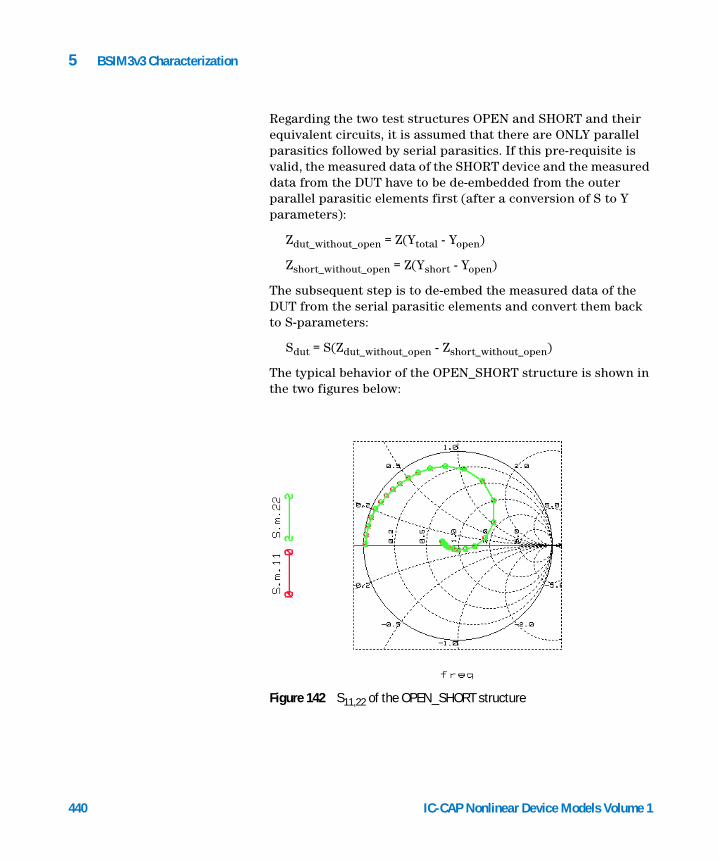
440
5 BSIM3v3 Characterization
Regarding the two test structures OPEN and SHORT and their equivalent circuits, it is assumed that there are ONLY parallel parasitics followed by serial parasitics. If this pre-requisite is valid, the measured data of the SHORT device and the measured data from the DUT have to be de-embedded from the outer parallel parasitic elements first (after a conversion of S to Y parameters):
Zdut_without_open = Z(Ytotal - Yopen)
Zshort_without_open = Z(Yshort - Yopen)
The subsequent step is to de-embed the measured data of the DUT from the serial parasitic elements and convert them back to S-parameters:
Sdut = S(Zdut_without_open - Zshort_without_open)
The typical behavior of the OPEN_SHORT structure is shown in the two figures below:
Figure 142 S11,22 of the OPEN_SHORT structure
IC-CAP Nonlinear Device Models Volume 1
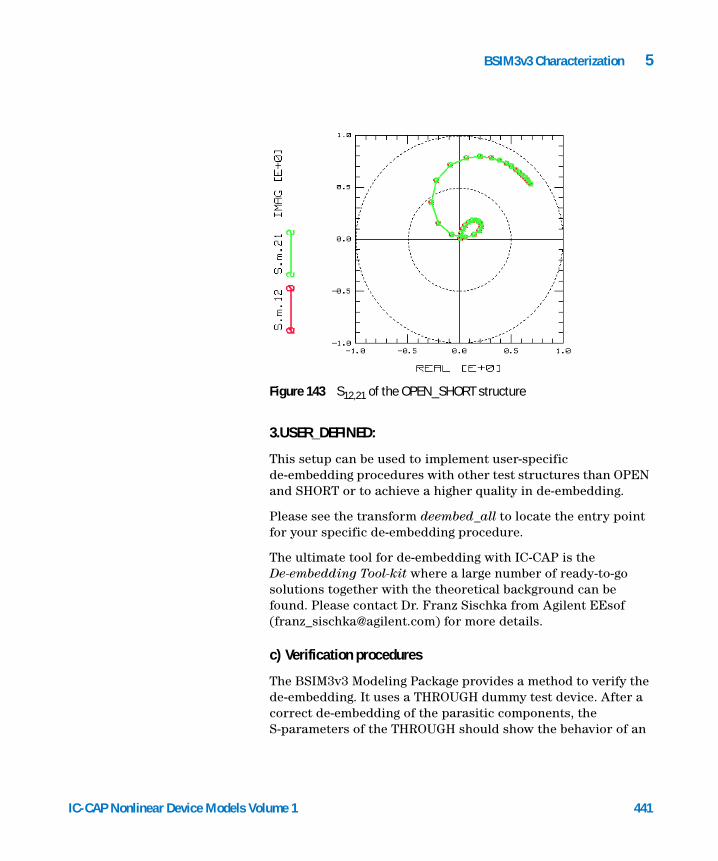
BSIM3v3 Characterization 5
IC-CAP Nonlinear Device Models Vo
3.USER_DEFINED:This setup can be used to implement user-specific de-embedding procedures with other test structures than OPEN and SHORT or to achieve a higher quality in de-embedding.
Please see the transform deembed_all to locate the entry point for your specific de-embedding procedure.
The ultimate tool for de-embedding with IC-CAP is the De-embedding Tool-kit where a large number of ready-to-go solutions together with the theoretical background can be found. Please contact Dr. Franz Sischka from Agilent EEsof ([email protected]) for more details.
c) Verification procedures
The BSIM3v3 Modeling Package provides a method to verify the de-embedding. It uses a THROUGH dummy test device. After a correct de-embedding of the parasitic components, the S-parameters of the THROUGH should show the behavior of an
Figure 143 S12,21 of the OPEN_SHORT structure
lume 1 441
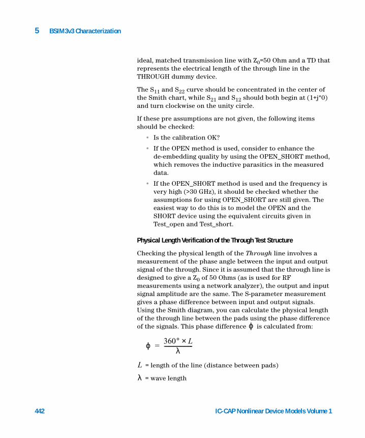
442
5 BSIM3v3 Characterization
ideal, matched transmission line with Z0=50 Ohm and a TD that represents the electrical length of the through line in the THROUGH dummy device.
The S11 and S22 curve should be concentrated in the center of the Smith chart, while S21 and S12 should both begin at (1+j*0) and turn clockwise on the unity circle.
If these pre assumptions are not given, the following items should be checked:
• Is the calibration OK?
• If the OPEN method is used, consider to enhance the de-embedding quality by using the OPEN_SHORT method, which removes the inductive parasitics in the measured data.
• If the OPEN_SHORT method is used and the frequency is very high (>30 GHz), it should be checked whether the assumptions for using OPEN_SHORT are still given. The easiest way to do this is to model the OPEN and the SHORT device using the equivalent circuits given in Test_open and Test_short.
Physical Length Verification of the Through Test Structure
Checking the physical length of the Through line involves a measurement of the phase angle between the input and output signal of the through. Since it is assumed that the through line is designed to give a Z0 of 50 Ohms (as is used for RF measurements using a network analyzer), the output and input signal amplitude are the same. The S-parameter measurement gives a phase difference between input and output signals. Using the Smith diagram, you can calculate the physical length of the through line between the pads using the phase difference of the signals. This phase difference is calculated from:
= length of the line (distance between pads)
= wave length
ϕ
ϕ 360° L×λ---------------------=
L
λ
IC-CAP Nonlinear Device Models Volume 1

BSIM3v3 Characterization 5
IC-CAP Nonlinear Device Models Vo
= speed of light = m/s
Since , the electrical length of the line is
The formulas above are valid only for air as dielectricum, since the velocity of the wave depends on the relative dielectric and permeable constants of the material. Building standard test structures on silicon wafers using silicon dioxide as dielectric, changes the propagation velocity of the waves from light speed (c) to:
The constants for silicon and silicon dioxide are:
c 38×10
λ cf--=
Lϕ c⋅
360° f⋅-----------------=
vpc
εr µr×--------------------=
Material
Silicon 1 11.8
Silicon dioxide 1 3.9
µr εr
Typically, the test structures are built on a silicon wafer on top of the silicon dioxide isolator. This leads us to a propagation velocity of:
Using this result, the physical length of the line would be:
vpc
εr µr×--------------------
c
3.9 -------------
c1.975-------------= = =
Lϕ c⋅
360° f⋅-----------------ϕ c⋅
360° f⋅( ) 1.975⋅----------------------------------------= =
lume 1 443

444
5 BSIM3v3 Characterization
Example
A measurement gives a phase difference between input and output of a through line as 10° at a frequency of 5 GHz. The test structure uses silicon dioxide as the isolator material. We would like to know the electrical length of our through test structure. Using the above formula leads to:
Therefore, the physical length of the measured line is 0.84E-3 m or 840 µm.
Lϕ c⋅
360° f⋅( ) 1.975⋅----------------------------------------
10° 38×10⋅
360° 59×10 1.975⋅ ⋅
------------------------------------------------- 0.84E-3= = =
IC-CAP Nonlinear Device Models Volume 1
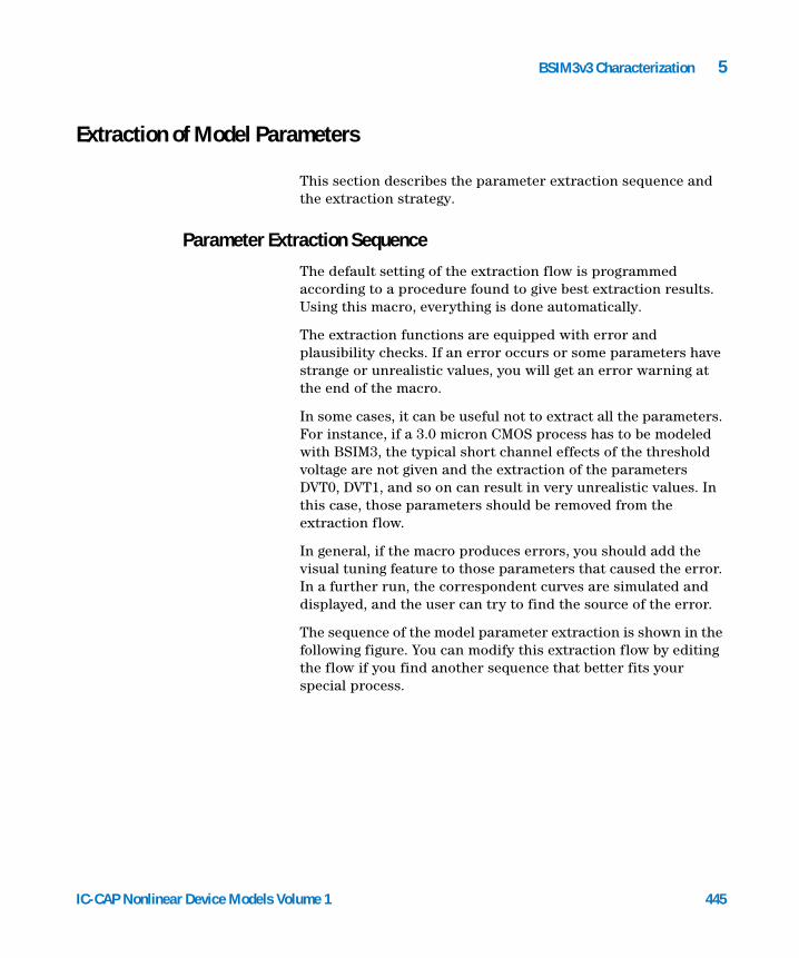
BSIM3v3 Characterization 5
Extraction of Model Parameters
IC-CAP Nonlinear Device Models Vo
This section describes the parameter extraction sequence and the extraction strategy.
Parameter Extraction Sequence
The default setting of the extraction flow is programmed according to a procedure found to give best extraction results. Using this macro, everything is done automatically.
The extraction functions are equipped with error and plausibility checks. If an error occurs or some parameters have strange or unrealistic values, you will get an error warning at the end of the macro.
In some cases, it can be useful not to extract all the parameters. For instance, if a 3.0 micron CMOS process has to be modeled with BSIM3, the typical short channel effects of the threshold voltage are not given and the extraction of the parameters DVT0, DVT1, and so on can result in very unrealistic values. In this case, those parameters should be removed from the extraction flow.
In general, if the macro produces errors, you should add the visual tuning feature to those parameters that caused the error. In a further run, the correspondent curves are simulated and displayed, and the user can try to find the source of the error.
The sequence of the model parameter extraction is shown in the following figure. You can modify this extraction flow by editing the flow if you find another sequence that better fits your special process.
lume 1 445
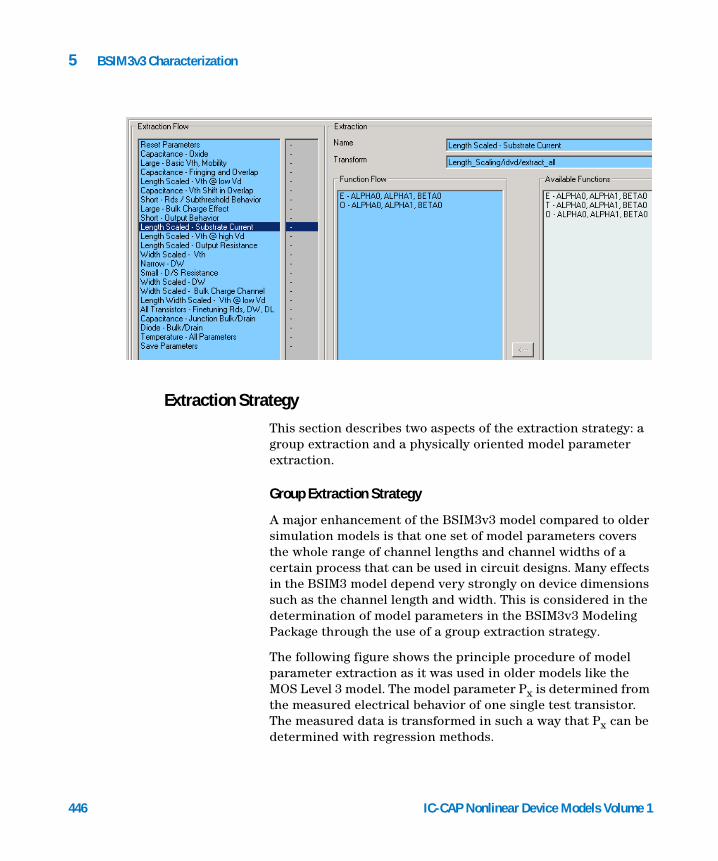
446
5 BSIM3v3 Characterization
Extraction Strategy
This section describes two aspects of the extraction strategy: a group extraction and a physically oriented model parameter extraction.
Group Extraction Strategy
A major enhancement of the BSIM3v3 model compared to older simulation models is that one set of model parameters covers the whole range of channel lengths and channel widths of a certain process that can be used in circuit designs. Many effects in the BSIM3 model depend very strongly on device dimensions such as the channel length and width. This is considered in the determination of model parameters in the BSIM3v3 Modeling Package through the use of a group extraction strategy.
The following figure shows the principle procedure of model parameter extraction as it was used in older models like the MOS Level 3 model. The model parameter Px is determined from the measured electrical behavior of one single test transistor. The measured data is transformed in such a way that Px can be determined with regression methods.
IC-CAP Nonlinear Device Models Volume 1
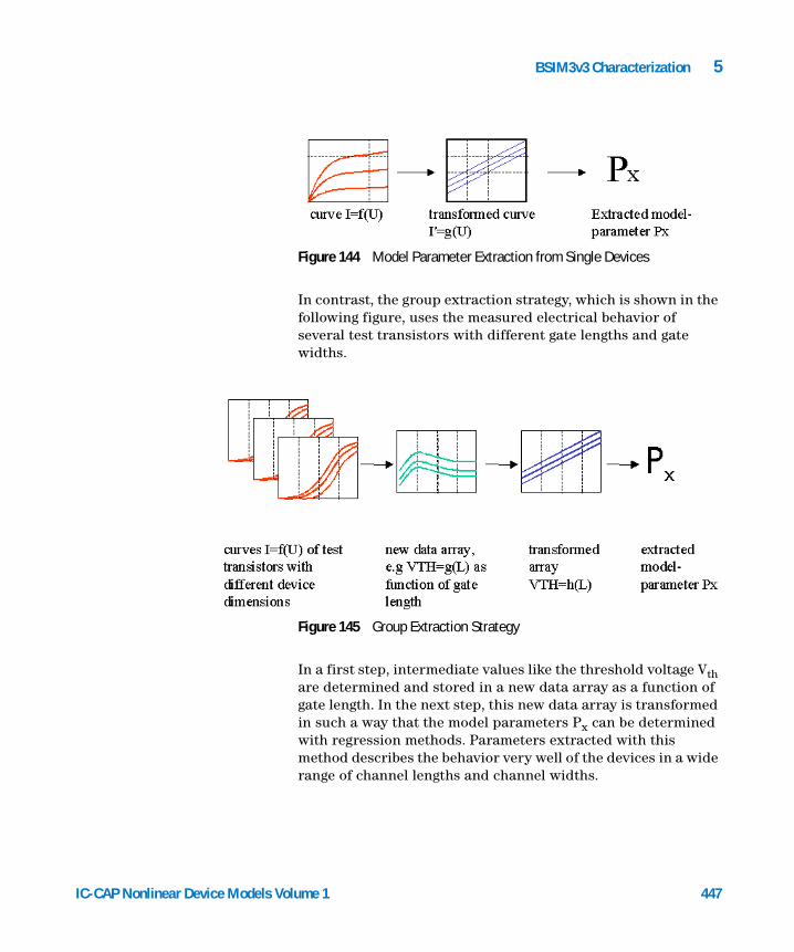
BSIM3v3 Characterization 5
IC-CAP Nonlinear Device Models Vo
In contrast, the group extraction strategy, which is shown in the following figure, uses the measured electrical behavior of several test transistors with different gate lengths and gate widths.
In a first step, intermediate values like the threshold voltage Vth are determined and stored in a new data array as a function of gate length. In the next step, this new data array is transformed in such a way that the model parameters Px can be determined with regression methods. Parameters extracted with this method describes the behavior very well of the devices in a wide range of channel lengths and channel widths.
Figure 144 Model Parameter Extraction from Single Devices
Figure 145 Group Extraction Strategy
lume 1 447
448
5 BSIM3v3 Characterization
Physically Oriented Model Parameter Extraction
For the determination of device model parameters from measured I-V or C-V curves, usually two general principles are applied—the optimization of the simulated device behavior or the parameter extraction based on the device equation.
The basis of the optimization process is the simulation of a device with exactly the same inputs (voltages, currents) that are used to measure the device. The error between simulated and measured data is the cost function for the optimization algorithms, which changes certain model parameters of the device, re-simulates it, and checks whether the error has increased or decreased. The advantage of this procedure is that the fitting between the measured curves and the simulated ones can be very good because the optimizer always tries to minimize this difference. However, in order to achieve this very good fitting, the optimization algorithm can give the model parameter physically unreasonable values. Another disadvantage is that many optimization algorithms are not able to find the global minimum of the failure function, which is the difference between measurement and simulation, and the success of the optimization depends on the start values of the model parameters. The last difficulty that can arise by using pure optimization algorithms for the model parameter determination is that the boundaries for the optimization process must be set very carefully. This means that the user of the optimization algorithm must have good knowledge about the device model and where the different model parameters have their influence on the device behavior in order to restrict the optimization process to a certain range of data.
In contrast to the optimization strategy, the extraction strategy is strictly based upon the device equations. If these device equations are physically oriented, as in the case of the BSIM3v3 model for MOS transistors, the extraction of the model parameters must give an accurate and realistic representation of the device physics. The basic idea of this extraction strategy is to transform measured data into such a form that model parameters of a certain part of the device equations can be derived by mathematical regression methods. The extraction routines must therefore incorporate much more knowledge
IC-CAP Nonlinear Device Models Volume 1
BSIM3v3 Characterization 5
IC-CAP Nonlinear Device Models Vo
about the model and its behavior. Generally, model parameters extracted in this way are more realistic and physically oriented. However, the fitting between the measured and simulated curves can be less accurate than in the case of an optimization, because the extraction method gives a realistic physical representation of the device while the optimization only targets a minimum error between measurement and simulations.
Figure 147 shows the principle data flow of such an extraction routine for the short channel model parameters DVT0 and DVT1. In this example, the threshold voltage Vth of several test transistors with different gate lengths is determined and stored in an intermediate data array. The short channel effect ∆Vth is isolated in the next step from Vth as a function of gate length and bulk voltage Vbs. The following figure shows ∆Vth as a function of those two variables. Only a subset of this data array is used for the determination of DVT0 and DVT1, and the boundaries for defining this subset are set by the extraction routine. As shown in the flowchart in Figure 147, different results from this action are possible. In the first case, no data point is available for the extraction and the user is informed with a warning message. This may occur for instance after measurement errors or with old CMOS processes that do not show a short channel effect. As a further possible result, only one usable data point is returned. From this data point, one model parameter can be determined while the second one has to be set to its default value.
lume 1 449
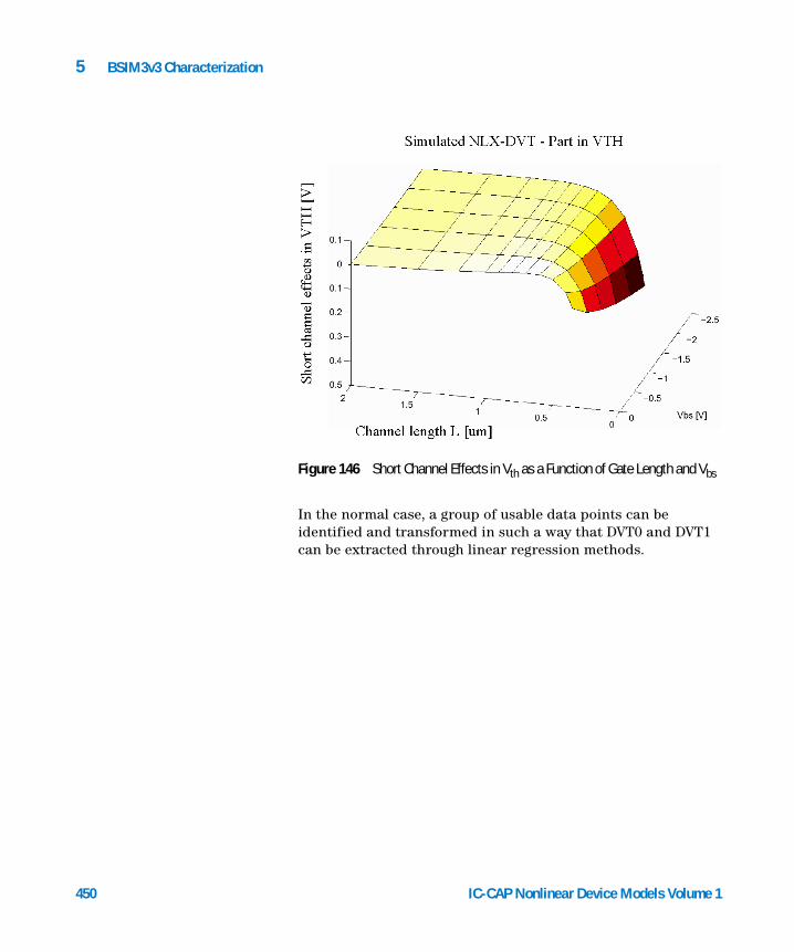
450
5 BSIM3v3 Characterization
In the normal case, a group of usable data points can be identified and transformed in such a way that DVT0 and DVT1 can be extracted through linear regression methods.
Figure 146 Short Channel Effects in Vth as a Function of Gate Length and Vbs
IC-CAP Nonlinear Device Models Volume 1
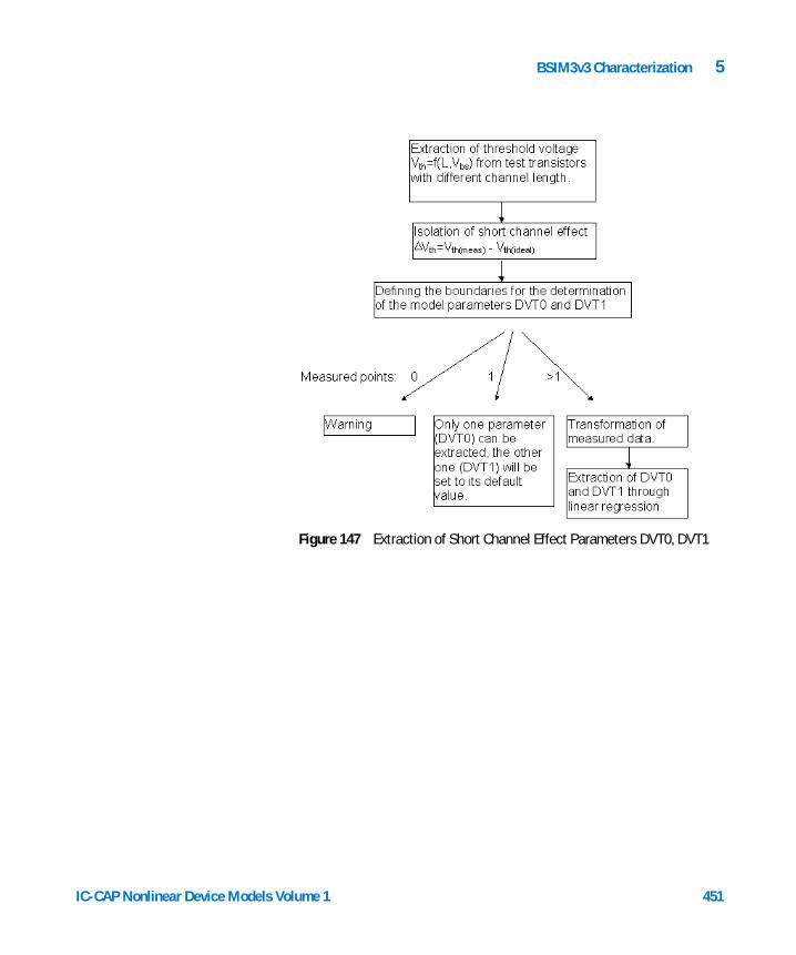
BSIM3v3 Characterization 5
IC-CAP Nonlinear Device Models Vo
Figure 147 Extraction of Short Channel Effect Parameters DVT0, DVT1
lume 1 451

5 BSIM3v3 Characterization
Binning of Model Parameters
Usage of binned models in a simulator
452
The binning idea
The idea of binning is to provide different model parameter sets for a scalable model (e.g., a MOS device) according to the device dimensions. In the case of MOSFETs, the validity of such a parameter set is determined by LMIN, LMAX, WMIN, WMAX for each bin.
Major commercial simulators like HSPICE, Spectre, and ADS support the binning feature for semiconductor models. However, it is not included in standard UC Berkeley SPICE3f5!
Lets take the example shown in the diagram above: we have 4 different bins with 4 different parameter sets. If we look only at the bins with the smallest width (see the arrow above), we still have 2 different parameter sets: set #1 and set #2.
The simulator would take the bins according to the following table:
Figure 148 Binned model according to the measured devices
g
IC-CAP Nonlinear Device Models Volume 1
BSIM3v3 Characterization 5
IC-CAP Nonlinear Device Models Vo
Please note: LMAX(bin1) = LMIN(bin2)
The simulator now calculates an effective model parameter P(L) from the different binned parameter sets and the actual gate length of the device to simulate.
In addition, inside a certain bin, the parameter itself is interpolated so that we end up with the following diagram:
Table 70 Bin Conditions
L < LMIN(bin1) Error: not specified!
LMIN(bin1) ≤ L < LMAX(bin1) BIN1 interpolated
LMIN(bin2) ≤ L < LMAX(bin2) BIN2 interpolated
L ≥ LMAX(bin2) Error: not specified!
Figure 149 Calculation of binned model parameters
lume 1 453
454
5 BSIM3v3 Characterization
Advanced binning approaches
As the diagram in the previous figure clearly shows, the model is defined only inside the gate length of the characterized devices. This is a critical condition, because the following two scenarios are very common for MOS devices:
• It is very usual to use a transistor with, for example, L = 10 µm as the largest measured device and to extrapolate the parameter set to devices with larger gate lengths. This is not a problem because the 10 um transistor already behaves like an ideal MOS transistor without short and narrow channel effects.
• For statistical simulations, the gate length and widths are overlaid by a statistical variation to reflect variations in lithography. If gate length or gate width are already at the boundary of the available model bins, this would not work.
Both described effects would cause no problem using the normal BSIM3 or BSIM4 model without binning. However, having the restrictions of the binning implementation in the simulators, the following two alternatives would help to overcome this bottleneck.
Extension of binning to include virtual devices
The first idea is to add additional model sets for areas in the L-W-space, which are not fully covered by measured devices. The following diagram shows such a scenario:
IC-CAP Nonlinear Device Models Volume 1
BSIM3v3 Characterization 5
IC-CAP Nonlinear Device Models Vo
The binned model parameter sets for region 1 through 4 have been determined from measured devices. Now, for the generation of the parameter set of region 9, it is assumed that the parameters for device d are equal to the parameters of device c and parameters from h are equal the parameters from g. The gate length of d and h are selected so large, that they cover all useful applications. The diagram in the following figure shows the principal calculation of the parameter P over an available range of gate lengths L.
Figure 150 Extension of binning
lume 1 455
456
5 BSIM3v3 Characterization
Figure 151 Calculation of binned model parameters with extensions
Extraction of binned model parameters
General algorithm
• For each device Di, at the boundary of the bins, the original parameter Poi = Pi is determined using a circuit/model parameter set without the binning feature!
• For each bin, the parameter is interpolated for the actual length and width according to the following equation:
P(L, W)i = Pi + PLi/Leff + PWi/Weff + PPi/(Weff Leff)
• The binning parameters Pi, PLi, PWi, PPi for one bin must be determined from the original parameters Poi and Poi+1. This is also very important to make sure that the parameter P is continuous at the boundary between two bins. That’s the reason why the devices at the edges of a bin are used to determine the parameters!
Poi original model parameter, for example, VTH0 extracted separately for each device
IC-CAP Nonlinear Device Models Volume 1

BSIM3v3 Characterization 5
IC-CAP Nonlinear Device Models Vo
For BSIM3:
For BSIM4:
P(L)i finally used interpolated model parameter inside a bin (internal SPICE value)
Pi constant model parameter inside a bin (in model parameter set)Please note: this is the same parameter as Poi but with a different meaning!
PLi length dependant model parameter inside a bin (in model parameter set)
PWi width dependant model parameter inside a bin (in model parameter set)
PPi length-width dependant model parameter inside a bin (in model parameter set)
Leff effective gate length
Weff effective gate width
Leff Ldes 2 LINTLL
LdesLLN
----------------LW
WdesLWN
------------------LWL
LdesLLN
WdesLWN
---------------------------------+ + +
–=
Weff Wdes 2 WINTWL
LdesWLN
------------------WW
WdesWWN
-------------------WWL
LdesWLN
WdesWWN
------------------------------------+ + +
–=
Leff Ldes XL 2 LINTLL
LdesLLN
----------------LW
WdesNF
-------------
LWN--------------------------------
LWL
LdesLLN Wdes
NF-------------
LWN------------------------------------------------+ + +
–+=
Weff
WdesNF
-------------- XW 2 WINTWL
LdesWLN
------------------WW
WdesNF
--------------
WWN-----------------------------------
WWL
LdesWLN Wdes
NF--------------
WWN----------------------------------------------------+ + +
–+=
lume 1 457
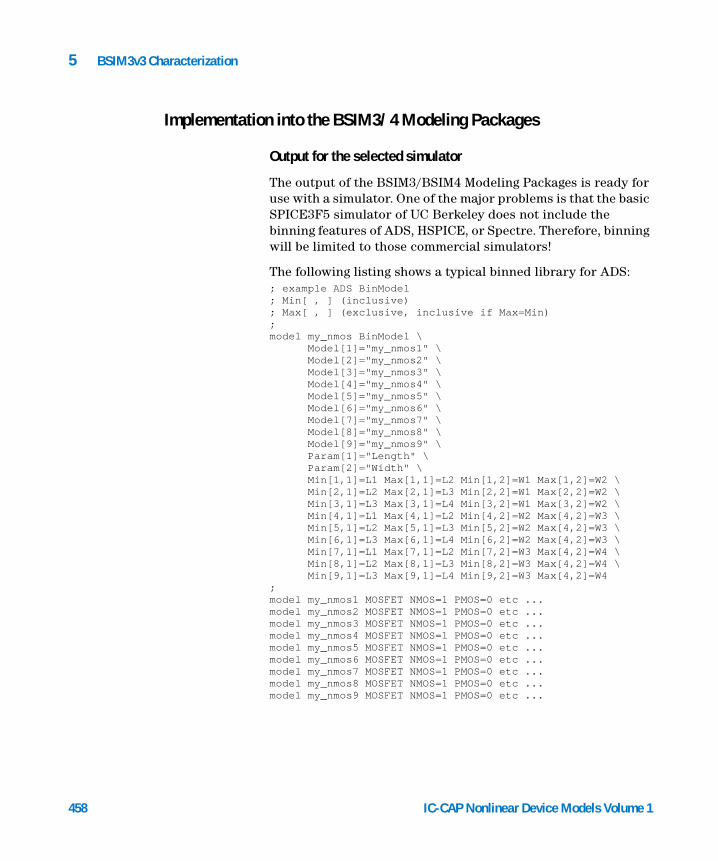
5 BSIM3v3 Characterization
Implementation into the BSIM3/4 Modeling Packages
458
Output for the selected simulator
The output of the BSIM3/BSIM4 Modeling Packages is ready for use with a simulator. One of the major problems is that the basic SPICE3F5 simulator of UC Berkeley does not include the binning features of ADS, HSPICE, or Spectre. Therefore, binning will be limited to those commercial simulators!
The following listing shows a typical binned library for ADS:; example ADS BinModel; Min[ , ] (inclusive); Max[ , ] (exclusive, inclusive if Max=Min);model my_nmos BinModel \ Model[1]="my_nmos1" \ Model[2]="my_nmos2" \ Model[3]="my_nmos3" \ Model[4]="my_nmos4" \ Model[5]="my_nmos5" \ Model[6]="my_nmos6" \ Model[7]="my_nmos7" \ Model[8]="my_nmos8" \ Model[9]="my_nmos9" \ Param[1]="Length" \ Param[2]="Width" \ Min[1,1]=L1 Max[1,1]=L2 Min[1,2]=W1 Max[1,2]=W2 \ Min[2,1]=L2 Max[2,1]=L3 Min[2,2]=W1 Max[2,2]=W2 \ Min[3,1]=L3 Max[3,1]=L4 Min[3,2]=W1 Max[3,2]=W2 \ Min[4,1]=L1 Max[4,1]=L2 Min[4,2]=W2 Max[4,2]=W3 \ Min[5,1]=L2 Max[5,1]=L3 Min[5,2]=W2 Max[4,2]=W3 \ Min[6,1]=L3 Max[6,1]=L4 Min[6,2]=W2 Max[4,2]=W3 \ Min[7,1]=L1 Max[7,1]=L2 Min[7,2]=W3 Max[4,2]=W4 \ Min[8,1]=L2 Max[8,1]=L3 Min[8,2]=W3 Max[4,2]=W4 \ Min[9,1]=L3 Max[9,1]=L4 Min[9,2]=W3 Max[4,2]=W4;model my_nmos1 MOSFET NMOS=1 PMOS=0 etc ...model my_nmos2 MOSFET NMOS=1 PMOS=0 etc ...model my_nmos3 MOSFET NMOS=1 PMOS=0 etc ...model my_nmos4 MOSFET NMOS=1 PMOS=0 etc ...model my_nmos5 MOSFET NMOS=1 PMOS=0 etc ...model my_nmos6 MOSFET NMOS=1 PMOS=0 etc ...model my_nmos7 MOSFET NMOS=1 PMOS=0 etc ...model my_nmos8 MOSFET NMOS=1 PMOS=0 etc ...model my_nmos9 MOSFET NMOS=1 PMOS=0 etc ...
IC-CAP Nonlinear Device Models Volume 1
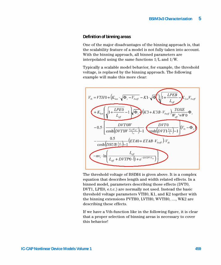
BSIM3v3 Characterization 5
IC-CAP Nonlinear Device Models Vo
Definition of binning areas
One of the major disadvantages of the binning approach is, that the scalability feature of a model is not fully taken into account. With the binning approach, all binned parameters are interpolated using the same functions 1/L and 1/W.
Typically a scalable model behavior, for example, the threshold voltage, is replaced by the binning approach. The following example will make this more clear:
The threshold voltage of BSIM4 is given above. It is a complex equation that describes length and width related effects. In a binned model, parameters describing those effects (DVT0, DVT1, LPE0, e.t.c.) are normally not used. Instead the basic threshold voltage parameters VTH0, K1, and K2 together with the binning extensions PVTH0, LVTH0, WVTH0, ...., WK2 are describing these effects.
If we have a Vth-function like in the following figure, it is clear that a proper selection of binning areas is necessary to cover this behavior!
lume 1 459

460
5 BSIM3v3 Characterization
Figure 152 Typical Vth behavior of a 0.18um CMOS process (n-type)
Figure 153 Two different binning scenarios
IC-CAP Nonlinear Device Models Volume 1
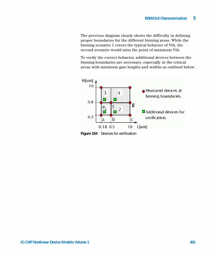
BSIM3v3 Characterization 5
IC-CAP Nonlinear Device Models Vo
The previous diagram clearly shows the difficulty in defining proper boundaries for the different binning areas. While the binning scenario 1 covers the typical behavior of Vth, the second scenario would miss the point of maximum Vth.
To verify the correct behavior, additional devices between the binning boundaries are necessary, especially in the critical areas with minimum gate lengths and widths as outlined below:
Figure 154 Devices for verification
g
lume 1 461
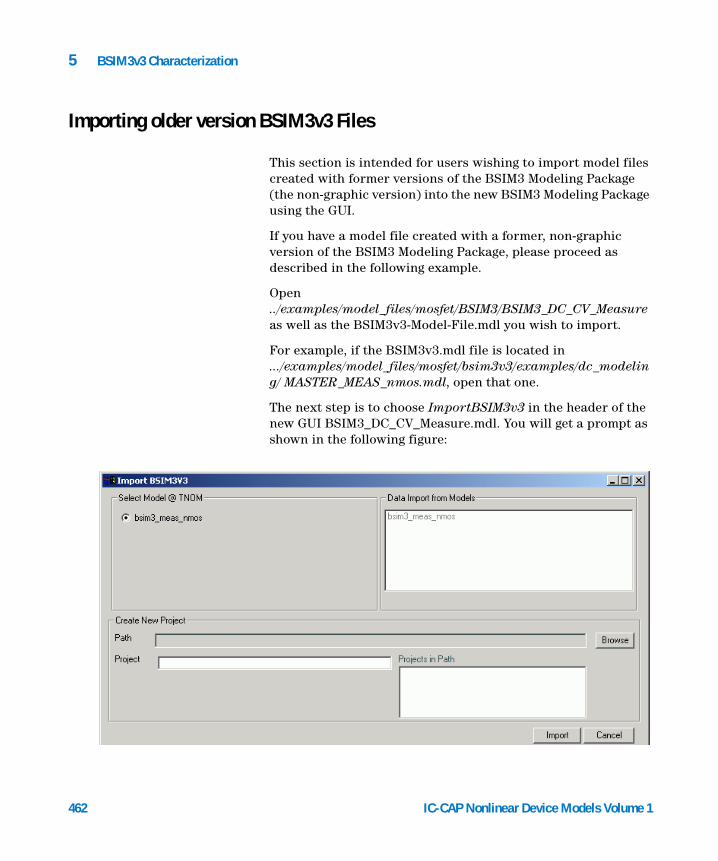
5 BSIM3v3 Characterization
Importing older version BSIM3v3 Files
462
This section is intended for users wishing to import model files created with former versions of the BSIM3 Modeling Package (the non-graphic version) into the new BSIM3 Modeling Package using the GUI.
If you have a model file created with a former, non-graphic version of the BSIM3 Modeling Package, please proceed as described in the following example.
Open ../examples/model_files/mosfet/BSIM3/BSIM3_DC_CV_Measure as well as the BSIM3v3-Model-File.mdl you wish to import.
For example, if the BSIM3v3.mdl file is located in .../examples/model_files/mosfet/bsim3v3/examples/dc_modeling/ MASTER_MEAS_nmos.mdl, open that one.
The next step is to choose ImportBSIM3v3 in the header of the new GUI BSIM3_DC_CV_Measure.mdl. You will get a prompt as shown in the following figure:
IC-CAP Nonlinear Device Models Volume 1

BSIM3v3 Characterization 5
IC-CAP Nonlinear Device Models Vo
Enter the name and location of the new BSIM3 project to be created and choose Import.
After the data is imported, you will get a message stating that the BSIM3v3-data has been successfully imported and you should go to the DC Transistor DUTs-folder, which looks like the following figure.
All transistors with the exception of the Large one are set to Additional.
Figure 155 Imported MASTER_MEAS_nmos.mdl from a former BSIM3v3 project
NOTE The DUT names already contain the functionality! This may be confusing, but you can change the names after the import procedure.
When starting the Size Category Set action, the following GUI appears:
lume 1 463

464
5 BSIM3v3 Characterization
Perform Auto Set and select Large_m as the Large Transistor inside the Set Category window.
Now the size categories are defined automatically and the resulting DCTransistorDUTs folder is shown in the following figure.
Figure 156 DC Transistor DUTs-folder after successful set size categories
IC-CAP Nonlinear Device Models Volume 1
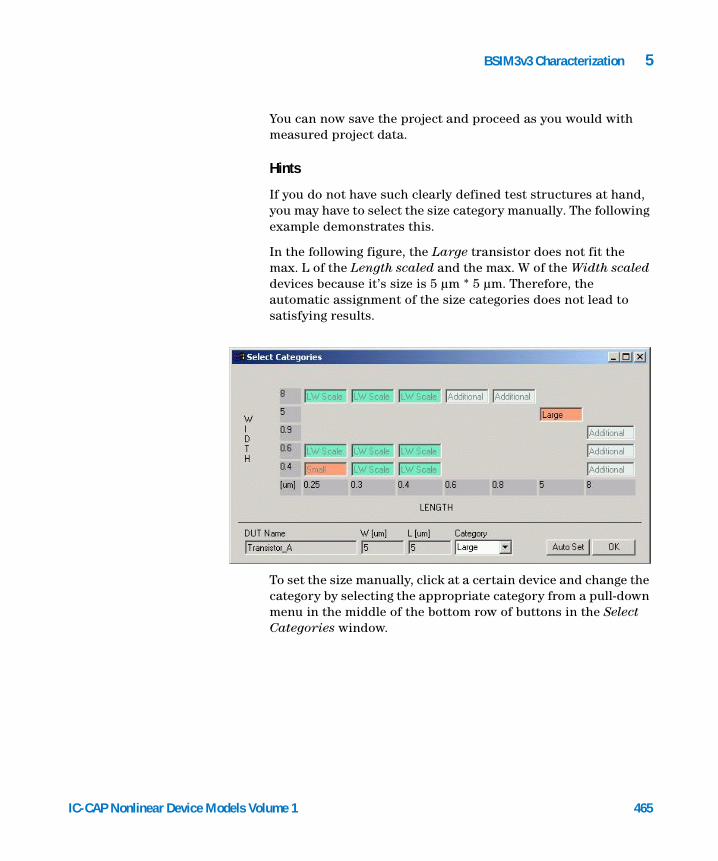
BSIM3v3 Characterization 5
IC-CAP Nonlinear Device Models Vo
You can now save the project and proceed as you would with measured project data.
Hints
If you do not have such clearly defined test structures at hand, you may have to select the size category manually. The following example demonstrates this.
In the following figure, the Large transistor does not fit the max. L of the Length scaled and the max. W of the Width scaled devices because it’s size is 5 µm * 5 µm. Therefore, the automatic assignment of the size categories does not lead to satisfying results.
To set the size manually, click at a certain device and change the category by selecting the appropriate category from a pull-down menu in the middle of the bottom row of buttons in the Select Categories window.
lume 1 465
5 BSIM3v3 Characterization
References
466
1 "BSIM3v3.3 Manual," University of California at Berkeley, July 2005
2 "Characterization System for Submicron CMOS Technologies," JESSI Reports AC41 94-1 through 94-6
3 Peter Klein, “A consistent parameter extraction method for deep submicron MOSFETs,” Proc. 27th European Solid-State Device Research Conference, Stuttgart, Germany, 1997
4 "Layout Rules for GHz Probing", Application Note Cascade Microtech
5 F. Sischka, "Deembedding Toolkit," Agilent, GmbH, Böblingen, Germany
6 File: "deemb_short_open.mdl" in IC-CAP examples, Agilent EEsof
7 W. Liu et al., “R.F. MOSFET Modeling Accounting for Distributed Substrate and Channel Resistances with Emphasis on the BSIM3v3 SPICE Model,” Proc. IEEE IEDM, 1997
8 C. Enz, “MOS Transistor Modeling for RF IC Design”, Silicon RF IC: Modeling and Simulation Workshop, Lausanne, Switzerland, 2000
9 M.Jamal Deen (Ed.), T.A.Fjeldly, “CMOS RF Modeling, Characterization and Applications”, Worldscientific, Co-authors: F.Sischka and T.Gneiting
10 W. Liu, “MOSFET Models for SPICE Simulation, including BSIM3v3 and BSIM4”, Wiley-Interscience, 2001
How to get the BSIM3v3 manual from University of Berkeley/California:
University of Berkeley/California provides an easy way to get a free copy of the BSIM3v3 manual and the BSIM3v3 source code from their world-wide web home page:
http://www-device.EECS.Berkeley.EDU/~bsim3/
Other useful internet addresses:
IC-CAP Nonlinear Device Models Volume 1
BSIM3v3 Characterization 5
IC-CAP Nonlinear Device Models Vo
Advanced Modeling Solutions:
http://www.admos.de
Agilent EEsof homepage
http://www.agilent.com/find/eesof/
Copyright
BSIM3 has been developed by the Device Research Group of the Department of Electrical Engineering and Computer Science, University of California, Berkeley and is copyrighted by the University of California.
lume 1 467

468
5 BSIM3v3 Characterization
IC-CAP Nonlinear Device Models Volume 1
Agilent 85190A IC-CAP 2008Nonlinear Device Models Volume 1
6MOS Model 9 Characterization
MOS Model 9 Model 471
The MM9 Model File 473
Parameter Extraction 505
Optimizing 510
The JUNCAP Model 513
References 530
MOS Model 9, developed by Philips, is a compact model for circuit simulation, suitable for both digital and analog applications. It provides the following features:
• Non-uniform doping effect on VTH
• Mobility reduction due to vertical field
• Vbs influence on mobility reduction
• Velocity saturation
• Channel length modulation
• Subthreshold conduction
• DIBL/Static-feedback
• Substrate current
• Parameter scaling with respect to W, L, and temperature
• Based on single-equation I-V and Q-V formulations
• Continuous gm, gm/Id and gds behavior in the weak to strong inversion and linear to saturation transition regions
This implementation is intended only for enhancement mode MOSFETs. Although MOS Model 9 also has applications for depletion mode devices, this implementation does not support
469Agilent Technologies

470
6 MOS Model 9 Characterization
this option. It is intended to work in the absence of a circuit simulator with MOS Model 9 being available to IC-CAP. Thus, the MOS Model 9 equations are implemented with C routines that are linked directly to the IC-CAP executable.
The suitability and accuracy for DC, AC and statistical applications have been demonstrated by Philips in several publications (see References [1], [2], and [3] at the end of this chapter).
IC-CAP Nonlinear Device Models Volume 1

MOS Model 9 Characterization 6
MOS Model 9 Model
IC-CAP Nonlinear Device Models Vo
MOS Model 9 uses two IC-CAP models: mm9 and mm9_tempx. Both of these models are stored in the file mm9.mdl. When saving in the Main window, ensure both model definitions are kept.
• mm9 is the main model definition file and contains the templates for measurements and extraction.
• mm9_tempx is the template file for data that will be measured at non-nominal temperature. The most important aspect of this file is that the MM9 parameter values are set to the values in the model MM9.
The primary method of model evaluation relies on the function MM9, which appears in the Function Group MM9. This function requires the inputs VD, VG, VS, and VB, which are arrays that give the drain, gate, source, and bulk voltages, respectively. It also requires the parameter Output, which controls the current returned by the function and is defined by one of the following options:
• D to return drain current
• S to return source current
• B to return bulk (avalanche) current
The calculations performed by this function are also influenced by two variables (MODLEVEL and EQNTYPE). These quantities and their influence are shown in Table 72.
The following figure illustrates the overall structure of the model.
lume 1 471
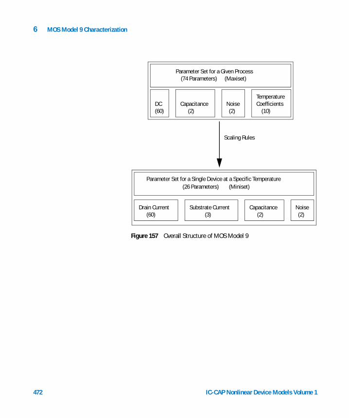
472
6 MOS Model 9 Characterization
Figure 157 Overall Structure of MOS Model 9
TemperatureCoefficients
(10)DC(60)
Capacitance(2)
Noise(2)
Parameter Set for a Given Process(74 Parameters) (Maxiset)
Noise(2)
Drain Current(60)
Capacitance(2)
Parameter Set for a Single Device at a Specific Temperature(26 Parameters) (Miniset)
Substrate Current(3)
Scaling Rules
IC-CAP Nonline
ar Device Mode ls Volume 1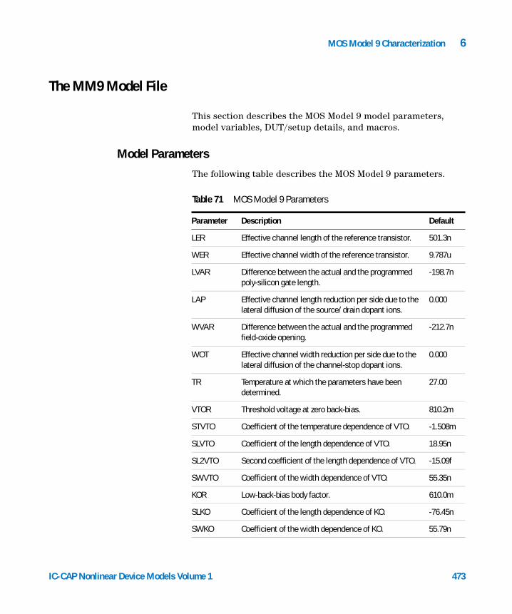
MOS Model 9 Characterization 6
The MM9 Model File
IC-CAP Nonlinear Device Models Vo
This section describes the MOS Model 9 model parameters, model variables, DUT/setup details, and macros.
Model Parameters
The following table describes the MOS Model 9 parameters.
Table 71 MOS Model 9 Parameters
Parameter Description Default
LER Effective channel length of the reference transistor. 501.3n
WER Effective channel width of the reference transistor. 9.787u
LVAR Difference between the actual and the programmed poly-silicon gate length.
-198.7n
LAP Effective channel length reduction per side due to the lateral diffusion of the source/drain dopant ions.
0.000
WVAR Difference between the actual and the programmed field-oxide opening.
-212.7n
WOT Effective channel width reduction per side due to the lateral diffusion of the channel-stop dopant ions.
0.000
TR Temperature at which the parameters have been determined.
27.00
VTOR Threshold voltage at zero back-bias. 810.2m
STVTO Coefficient of the temperature dependence of VTO. -1.508m
SLVTO Coefficient of the length dependence of VTO. 18.95n
SL2VTO Second coefficient of the length dependence of VTO. -15.09f
SWVTO Coefficient of the width dependence of VTO. 55.35n
KOR Low-back-bias body factor. 610.0m
SLKO Coefficient of the length dependence of KO. -76.45n
SWKO Coefficient of the width dependence of KO. 55.79n
lume 1 473

474
6 MOS Model 9 Characterization
KR High-back-bias body factor. 170.5m
SLK Coefficient of the length dependence of K. -293.1n
SWK Coefficient of the width dependence of K. 185.5n
VSBXR Transition voltage for the dual-k factor model. 1.926
SLVSBX Coefficient of the length dependence of VSBX. 443.2n
SWVSBX Coefficient of the width dependence of VSBX. -349.8n
BETSQ Gain factor. 155.9u
ETABET Exponent of the temperature dependence of the gain factor.
1.655
THE1R Coefficient of the mobility due to the gate induced field.
306.3m
STTHE1R Coefficient of the temperature dependence of THE1. -613.8u
SLTHE1R Coefficient of the length dependence of THE1. 66.10n
STLTHE1 Coefficient of the temperature dependence of the length dependence of THE1.
-95.78p
SWTHE1 Coefficient of the width dependence of THE1. -44.23n
THE2R Coefficient of the mobility due to the back-bias. 43.49m
STTHE2R Coefficient of the temperature dependence of THE2. 97.75u
SLTHE2R Coefficient of the length dependence of THE2. -56.97n
STLTHE2 Coefficient of the temperature dependence of the length dependence of THE2.
-13.64p
SWTHE2 Coefficient of the width dependence of THE2. 19.14n
THE3R Coefficient of the mobility due to the lateral field. 264.4m
STTHE3R Coefficient of the temperature dependence of THE3. 8.227u
SLTHE3R Coefficient of the length dependence of THE3. 135.8n
STLTHE3 Coefficient of the temperature dependence of the length dependence of THE3.
-509.4p
Table 71 MOS Model 9 Parameters
Parameter Description Default
IC-CAP Nonlinear Device Models Volume 1
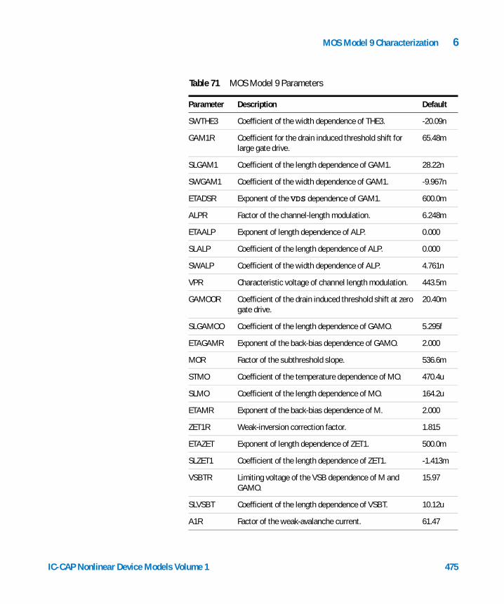
MOS Model 9 Characterization 6
IC-CAP Nonlinear Device Models Vo
SWTHE3 Coefficient of the width dependence of THE3. -20.09n
GAM1R Coefficient for the drain induced threshold shift for large gate drive.
65.48m
SLGAM1 Coefficient of the length dependence of GAM1. 28.22n
SWGAM1 Coefficient of the width dependence of GAM1. -9.967n
ETADSR Exponent of the VDS dependence of GAM1. 600.0m
ALPR Factor of the channel-length modulation. 6.248m
ETAALP Exponent of length dependence of ALP. 0.000
SLALP Coefficient of the length dependence of ALP. 0.000
SWALP Coefficient of the width dependence of ALP. 4.761n
VPR Characteristic voltage of channel length modulation. 443.5m
GAMOOR Coefficient of the drain induced threshold shift at zero gate drive.
20.40m
SLGAMOO Coefficient of the length dependence of GAMO. 5.295f
ETAGAMR Exponent of the back-bias dependence of GAMO. 2.000
MOR Factor of the subthreshold slope. 536.6m
STMO Coefficient of the temperature dependence of MO. 470.4u
SLMO Coefficient of the length dependence of MO. 164.2u
ETAMR Exponent of the back-bias dependence of M. 2.000
ZET1R Weak-inversion correction factor. 1.815
ETAZET Exponent of length dependence of ZET1. 500.0m
SLZET1 Coefficient of the length dependence of ZET1. -1.413m
VSBTR Limiting voltage of the VSB dependence of M and GAMO.
15.97
SLVSBT Coefficient of the length dependence of VSBT. 10.12u
A1R Factor of the weak-avalanche current. 61.47
Table 71 MOS Model 9 Parameters
Parameter Description Default
lume 1 475
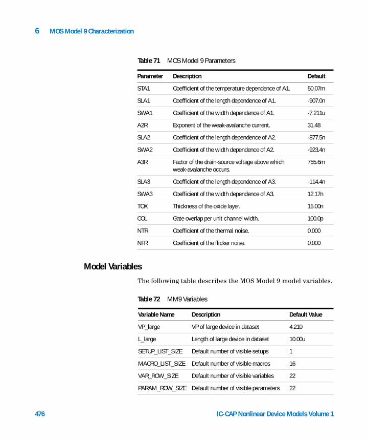
476
6 MOS Model 9 Characterization
STA1 Coefficient of the temperature dependence of A1. 50.07m
SLA1 Coefficient of the length dependence of A1. -907.0n
SWA1 Coefficient of the width dependence of A1. -7.211u
A2R Exponent of the weak-avalanche current. 31.48
SLA2 Coefficient of the length dependence of A2. -877.5n
SWA2 Coefficient of the width dependence of A2. -923.4n
A3R Factor of the drain-source voltage above which weak-avalanche occurs.
755.6m
SLA3 Coefficient of the length dependence of A3. -114.4n
SWA3 Coefficient of the width dependence of A3. 12.17n
TOX Thickness of the oxide layer. 15.00n
COL Gate overlap per unit channel width. 100.0p
NTR Coefficient of the thermal noise. 0.000
NFR Coefficient of the flicker noise. 0.000
Table 71 MOS Model 9 Parameters
Parameter Description Default
Model Variables
The following table describes the MOS Model 9 model variables.
Table 72 MM9 Variables
Variable Name Description Default Value
VP_large VP of large device in dataset 4.210
L_large Length of large device in dataset 10.00u
SETUP_LIST_SIZE Default number of visible setups 1
MACRO_LIST_SIZE Default number of visible macros 16
VAR_ROW_SIZE Default number of visible variables 22
PARAM_ROW_SIZE Default number of visible parameters 22
IC-CAP Nonlinear Device Models Volume 1
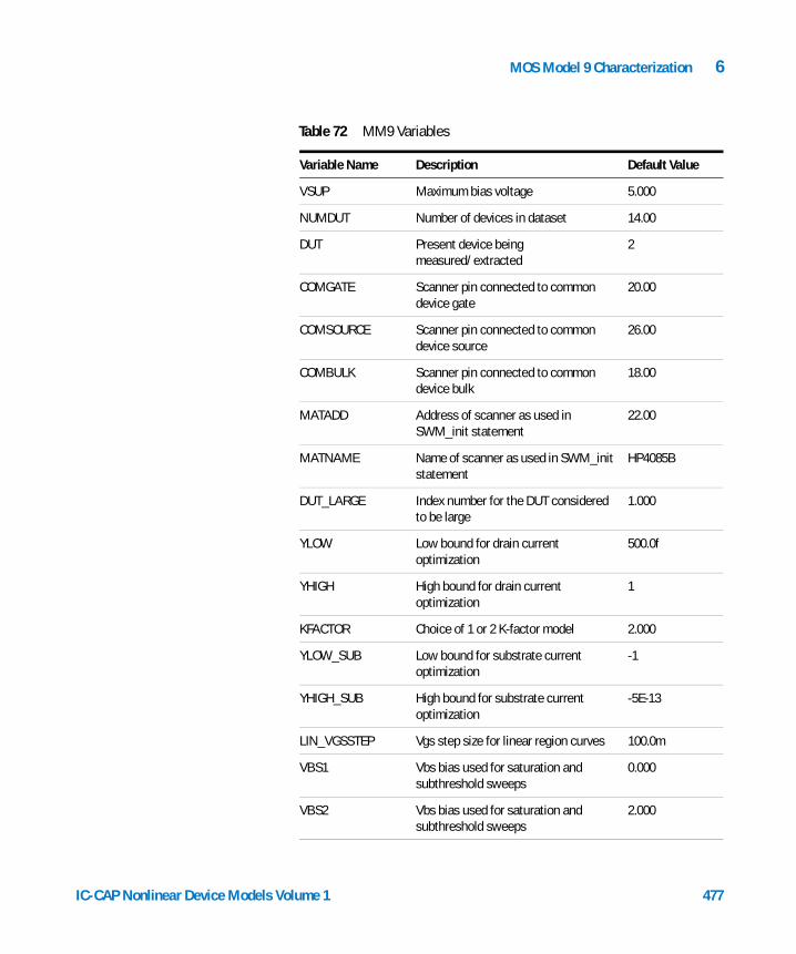
MOS Model 9 Characterization 6
IC-CAP Nonlinear Device Models Vo
VSUP Maximum bias voltage 5.000
NUMDUT Number of devices in dataset 14.00
DUT Present device being measured/extracted
2
COMGATE Scanner pin connected to common device gate
20.00
COMSOURCE Scanner pin connected to common device source
26.00
COMBULK Scanner pin connected to common device bulk
18.00
MATADD Address of scanner as used in SWM_init statement
22.00
MATNAME Name of scanner as used in SWM_init statement
HP4085B
DUT_LARGE Index number for the DUT considered to be large
1.000
YLOW Low bound for drain current optimization
500.0f
YHIGH High bound for drain current optimization
1
KFACTOR Choice of 1 or 2 K-factor model 2.000
YLOW_SUB Low bound for substrate current optimization
-1
YHIGH_SUB High bound for substrate current optimization
-5E-13
LIN_VGSSTEP Vgs step size for linear region curves 100.0m
VBS1 Vbs bias used for saturation and subthreshold sweeps
0.000
VBS2 Vbs bias used for saturation and subthreshold sweeps
2.000
Table 72 MM9 Variables
Variable Name Description Default Value
lume 1 477
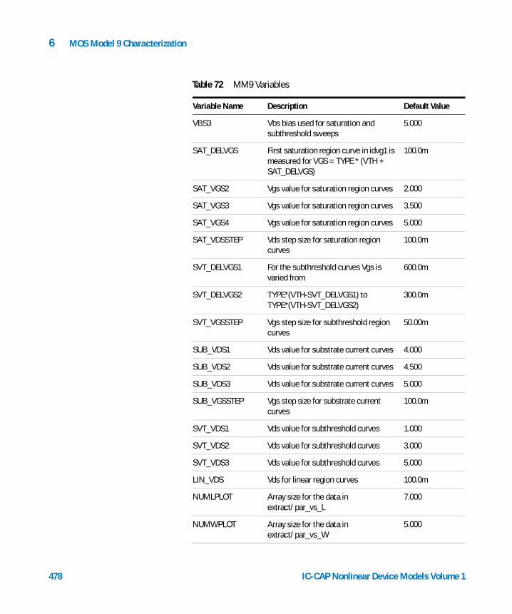
478
6 MOS Model 9 Characterization
VBS3 Vbs bias used for saturation and subthreshold sweeps
5.000
SAT_DELVGS First saturation region curve in idvg1 is measured for VGS = TYPE * (VTH + SAT_DELVGS)
100.0m
SAT_VGS2 Vgs value for saturation region curves 2.000
SAT_VGS3 Vgs value for saturation region curves 3.500
SAT_VGS4 Vgs value for saturation region curves 5.000
SAT_VDSSTEP Vds step size for saturation region curves
100.0m
SVT_DELVGS1 For the subthreshold curves Vgs is varied from
600.0m
SVT_DELVGS2 TYPE*(VTH-SVT_DELVGS1) to TYPE*(VTH-SVT_DELVGS2)
300.0m
SVT_VGSSTEP Vgs step size for subthreshold region curves
50.00m
SUB_VDS1 Vds value for substrate current curves 4.000
SUB_VDS2 Vds value for substrate current curves 4.500
SUB_VDS3 Vds value for substrate current curves 5.000
SUB_VGSSTEP Vgs step size for substrate current curves
100.0m
SVT_VDS1 Vds value for subthreshold curves 1.000
SVT_VDS2 Vds value for subthreshold curves 3.000
SVT_VDS3 Vds value for subthreshold curves 5.000
LIN_VDS Vds for linear region curves 100.0m
NUMLPLOT Array size for the data in extract/par_vs_L
7.000
NUMWPLOT Array size for the data in extract/par_vs_W
5.000
Table 72 MM9 Variables
Variable Name Description Default Value
IC-CAP Nonlinear Device Models Volume 1
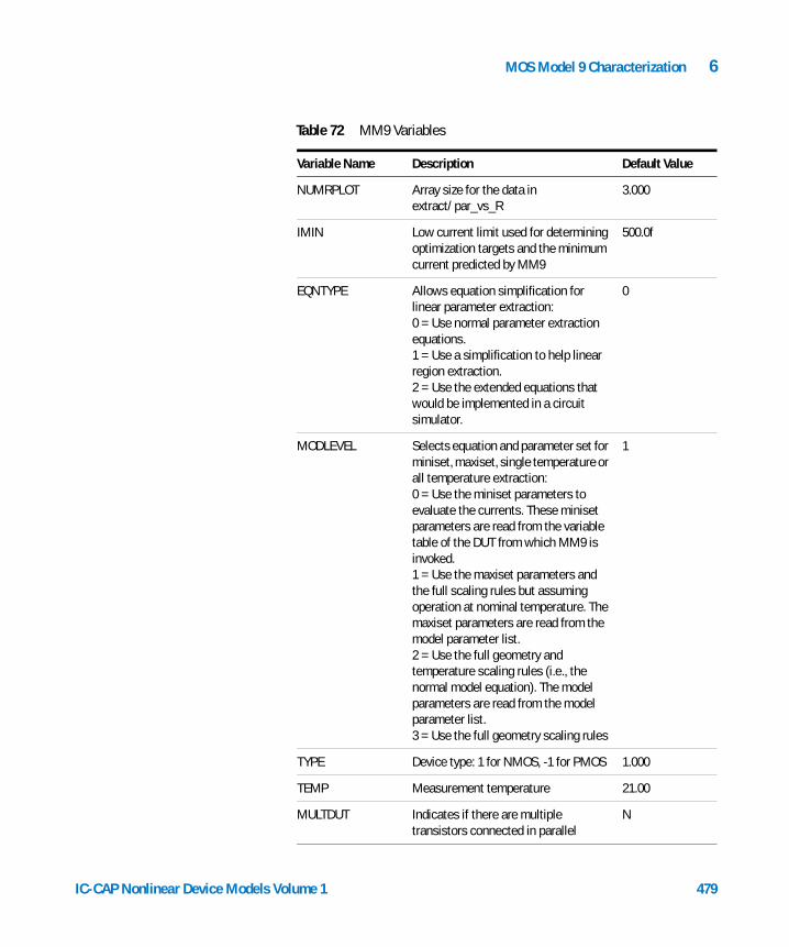
MOS Model 9 Characterization 6
IC-CAP Nonlinear Device Models Vo
NUMRPLOT Array size for the data in extract/par_vs_R
3.000
IMIN Low current limit used for determining optimization targets and the minimum current predicted by MM9
500.0f
EQNTYPE Allows equation simplification for linear parameter extraction:0 = Use normal parameter extraction equations.1 = Use a simplification to help linear region extraction.2 = Use the extended equations that would be implemented in a circuit simulator.
0
MODLEVEL Selects equation and parameter set for miniset, maxiset, single temperature or all temperature extraction:0 = Use the miniset parameters to evaluate the currents. These miniset parameters are read from the variable table of the DUT from which MM9 is invoked.1 = Use the maxiset parameters and the full scaling rules but assuming operation at nominal temperature. The maxiset parameters are read from the model parameter list.2 = Use the full geometry and temperature scaling rules (i.e., the normal model equation). The model parameters are read from the model parameter list.3 = Use the full geometry scaling rules
1
TYPE Device type: 1 for NMOS, -1 for PMOS 1.000
TEMP Measurement temperature 21.00
MULTDUT Indicates if there are multiple transistors connected in parallel
N
Table 72 MM9 Variables
Variable Name Description Default Value
lume 1 479
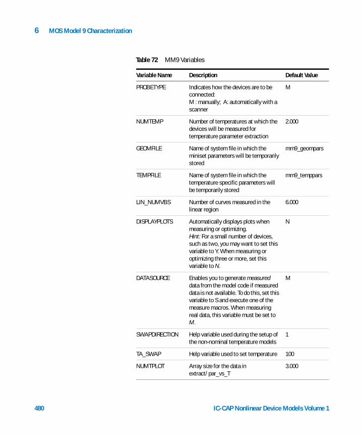
480
6 MOS Model 9 Characterization
PROBETYPE Indicates how the devices are to be connected:M : manually; A: automatically with a scanner
M
NUMTEMP Number of temperatures at which the devices will be measured for temperature parameter extraction
2.000
GEOMFILE Name of system file in which the miniset parameters will be temporarily stored
mm9_geompars
TEMPFILE Name of system file in which the temperature specific parameters will be temporarily stored
mm9_temppars
LIN_NUMVBS Number of curves measured in the linear region
6.000
DISPLAYPLOTS Automatically displays plots when measuring or optimizing. Hint: For a small number of devices, such as two, you may want to set this variable to Y. When measuring or optimizing three or more, set this variable to N.
N
DATASOURCE Enables you to generate measured data from the model code if measured data is not available. To do this, set this variable to S and execute one of the measure macros. When measuring real data, this variable must be set to M.
M
SWAPDIRECTION Help variable used during the setup of the non-nominal temperature models
1
TA_SWAP Help variable used to set temperature 100
NUMTPLOT Array size for the data in extract/par_vs_T
3.000
Table 72 MM9 Variables
Variable Name Description Default Value
IC-CAP Nonlinear Device Models Volume 1
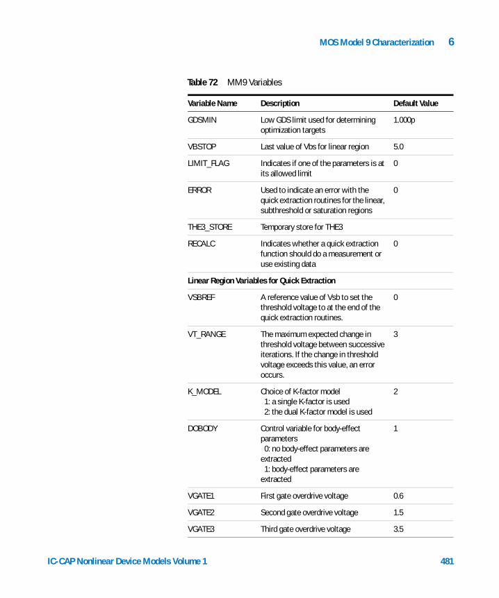
MOS Model 9 Characterization 6
IC-CAP Nonlinear Device Models Vo
GDSMIN Low GDS limit used for determining optimization targets
1.000p
VBSTOP Last value of Vbs for linear region 5.0
LIMIT_FLAG Indicates if one of the parameters is at its allowed limit
0
ERROR Used to indicate an error with the quick extraction routines for the linear, subthreshold or saturation regions
0
THE3_STORE Temporary store for THE3
RECALC Indicates whether a quick extraction function should do a measurement or use existing data
0
Linear Region Variables for Quick Extraction
VSBREF A reference value of Vsb to set the threshold voltage to at the end of the quick extraction routines.
0
VT_RANGE The maximum expected change in threshold voltage between successive iterations. If the change in threshold voltage exceeds this value, an error occurs.
3
K_MODEL Choice of K-factor model 1: a single K-factor is used 2: the dual K-factor model is used
2
DOBODY Control variable for body-effect parameters 0: no body-effect parameters are extracted 1: body-effect parameters are extracted
1
VGATE1 First gate overdrive voltage 0.6
VGATE2 Second gate overdrive voltage 1.5
VGATE3 Third gate overdrive voltage 3.5
Table 72 MM9 Variables
Variable Name Description Default Value
lume 1 481
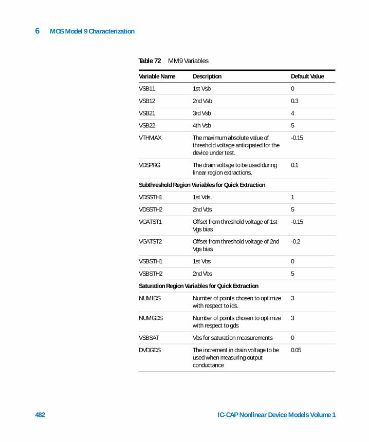
482
6 MOS Model 9 Characterization
VSB11 1st Vsb 0
VSB12 2nd Vsb 0.3
VSB21 3rd Vsb 4
VSB22 4th Vsb 5
VTHMAX The maximum absolute value of threshold voltage anticipated for the device under test.
-0.15
VDSPRG The drain voltage to be used during linear region extractions.
0.1
Subthreshold Region Variables for Quick Extraction
VDSSTH1 1st Vds 1
VDSSTH2 2nd Vds 5
VGATST1 Offset from threshold voltage of 1st Vgs bias
-0.15
VGATST2 Offset from threshold voltage of 2nd Vgs bias
-0.2
VSBSTH1 1st Vbs 0
VSBSTH2 2nd Vbs 5
Saturation Region Variables for Quick Extraction
NUMIDS Number of points chosen to optimize with respect to ids.
3
NUMGDS Number of points chosen to optimize with respect to gds
3
VSBSAT Vbs for saturation measurements 0
DVDGDS The increment in drain voltage to be used when measuring output conductance
0.05
Table 72 MM9 Variables
Variable Name Description Default Value
IC-CAP Nonlinear Device Models Volume 1
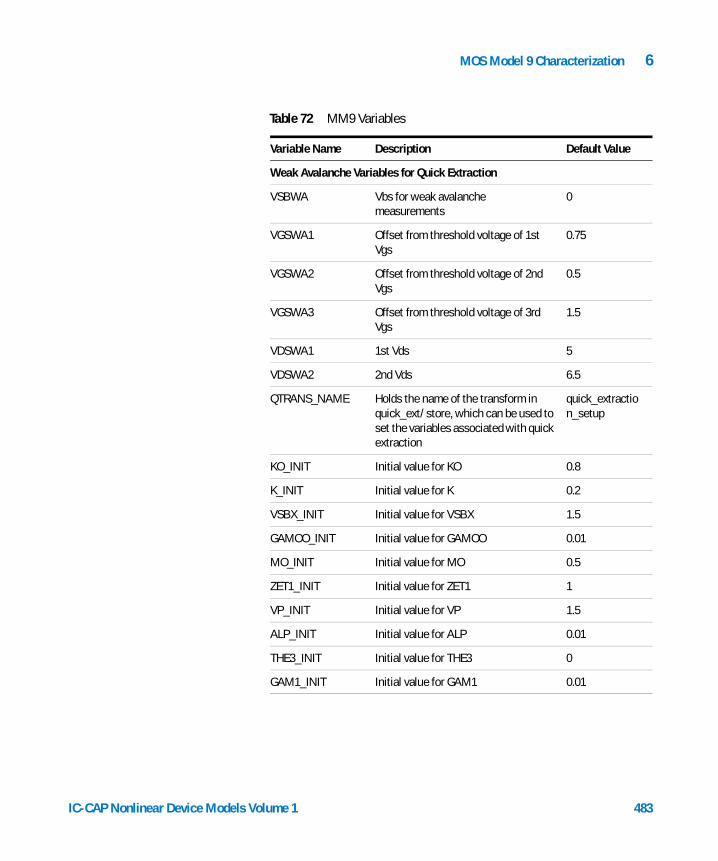
MOS Model 9 Characterization 6
IC-CAP Nonlinear Device Models Vo
Weak Avalanche Variables for Quick Extraction
VSBWA Vbs for weak avalanche measurements
0
VGSWA1 Offset from threshold voltage of 1st Vgs
0.75
VGSWA2 Offset from threshold voltage of 2nd Vgs
0.5
VGSWA3 Offset from threshold voltage of 3rd Vgs
1.5
VDSWA1 1st Vds 5
VDSWA2 2nd Vds 6.5
QTRANS_NAME Holds the name of the transform in quick_ext/store, which can be used to set the variables associated with quick extraction
quick_extraction_setup
KO_INIT Initial value for KO 0.8
K_INIT Initial value for K 0.2
VSBX_INIT Initial value for VSBX 1.5
GAMOO_INIT Initial value for GAMOO 0.01
MO_INIT Initial value for MO 0.5
ZET1_INIT Initial value for ZET1 1
VP_INIT Initial value for VP 1.5
ALP_INIT Initial value for ALP 0.01
THE3_INIT Initial value for THE3 0
GAM1_INIT Initial value for GAM1 0.01
Table 72 MM9 Variables
Variable Name Description Default Value
lume 1 483
6 MOS Model 9 Characterization
The extract DUT
484
The extract device contains all of the sequences used for the parameter optimizations and much of the setup information.
extract/devices holds setup information that has the form of an array. The input index is used to establish the size of the various arrays. Its size in turn is controlled by the variable NUMDUT from the model variable table. Note that the DUTs are labeled from 1 to the number of devices but the arrays holding the DUT information begin with index 0. The outputs for this setup are shown next.
The devices setup contains the following transforms:
connect calls SWM_init and Connect to connect the matrix for a particular device or prompts you to connect the device. It uses information contained in the outputs described for the setup devices.
dummy is an empty (apart from comments) PEL transform. It was found that when a variable that affects the array size in any setup (NUMDUT in this case) is changed from a C transform, then a call to a dummy transform is necessary to force IC-CAP to re-establish the proper array dimensions before attempting to write to these arrays.
width Holds the widths of the devices to be measured
length Holds the lengths of the devices to be measured
mult Holds the values for MULT for each device, that is, the number of similar structures connected in parallel.
drain Holds the matrix pin numbers connected to the drains (if a switching matrix is being used)
gate The matrix pin numbers connected to the gates
source The matrix pin numbers connected to the sources
bulk The matrix pin numbers connected to the bulks
dotemp An array that indicates if the devices are to be measured at temperature. If the value of dotemp for any device is set to 1, then this device will be measured at temperature.
IC-CAP Nonlinear Device Models Volume 1
MOS Model 9 Characterization 6
IC-CAP Nonlinear Device Models Vo
extract/single_ext contains the sequences for extracting the miniset parameters. The variable table of this setup contains a list of MIN and MAX values for use in the optimization steps. It is easier to modify the optimization limits from such a variable table rather than from the individual optimization transforms. For the extraction of a miniset for any particular DUT, this setup is first copied into the appropriate DUT. The optimizations then operate on the miniset variables local to that DUT.
The single_ext setup contains the following transforms:
full_extract is the controlling PEL for miniset extraction. For more information, refer to the discussion on full_extract in the section “Optimization Transforms and Macros” on page 510.
par_init initializes parameter (local variables in fact) values at the beginning of miniset extraction.
lin_opt1 is an optimization call for linear region fitting at Vbs = 0 for the parameters BET, THE1, and VTO
lin_opt2 is an optimization call for linear region fitting for all Vbs for the parameters KO, THE2, VSBX, and K. This transform is used for the case of the 2 k-factor model.
lin_opt3 is an optimization call for linear region fitting for all Vbs for the parameters KO and THE2. This transform is used for the case of the 1 k-factor model.
subvt_opt1 is an optimization call for subthreshold region fitting at Vbs = 0 for the parameters GAMOO, MO, and ZET1.
normal_gds_opt1 is an optimization call for gds fitting at Vbs = 0 for the normal devices and for the parameters GAM1 and ALP
large_gds_opt1 calls an optimization sequence for gds for the special case of the device with the largest length. This sequence in turn calls vp_opt and alp_opt.
vp_opt is an optimization call for gds fitting at Vbs = 0 for the parameter VP.
lume 1 485
486
6 MOS Model 9 Characterization
alp_opt is an optimization call for gds fitting at Vbs = 0 for the parameter ALP
set_VP sets the VP of any device by scaling of the VP of the large device.
set_VP_large sets a model level variable VP_large to hold the VP of the large device.
ids_opt1 is an optimization call for ids fitting at Vbs = 0 for the parameter THE3.
isub_opt1 is an optimization call for avalanche current fitting for Vbs = 0 for the parameters A1, A2, and A3.
subvt_opt2 is an optimization call for subthreshold region fitting for all Vbs for the parameter VSBT.
limit_check is called at the end of each miniset optimization to check the parameters with respect to the miniset limits. It is used by the macros extract_one_miniset and extract_all_minisets.
extract/scaled_ext contains the optimization sequences necessary for scaled (maxiset) extraction at the nominal temperature. The variable table of this setup contains the parameter MIN and MAX limits that will be used during optimization.
The scaled_ext setup contains the following transforms:
sim_all cause the currents in all the DUTs at the nominal temperature to be resimulated (i.e., evaluated with the MM9 C transform).
sca_opt controls the sequence for maxiset optimizations. For more information, refer to the discussion on sca_opt in the section “Optimization Transforms and Macros” on page 510.
read_sca_opt_files reads the definitions of the optimization transforms from the UNIX file system. When you execute SETUP, the number of devices may change and the optimization tables for maxiset extraction need to be rebuilt.
IC-CAP Nonlinear Device Models Volume 1

MOS Model 9 Characterization 6
IC-CAP Nonlinear Device Models Vo
This is performed by the C transform SETUP which writes the new optimization definitions to the file system. This transform then reads these new definitions back into IC-CAP.
sca_lin_opt1 is an optimization call for linear region fitting at Vbs = 0 for the parameters VTOR, SLVTO, SL2VTO, SWVTO, BETSQ, THE1R, SLTHE1R, and SWTHE1.
sca_lin_opt2 is an optimization call for linear region fitting at all Vbs for the parameters THE2R, SLTHE2R, SWTHE2, KOR, SLKO, SWKO, KR, SLK, SWK, VSBXR, SLVSBX, and SWVSBX. This sequence is used for the 2 k-factor model option.
sca_lin_opt3 is an optimization call for linear region fitting at all Vbs for the parameters THE2R, SLTHE2R, SWTHE2, KOR, SLKO, and SWKO. This sequence is used for the 1 k-factor model option.
sca_subvt_opt1 is an optimization call for subthreshold optimization at Vbs = 0 for the parameters GAMOOR, SLGAMOO, MOR, SLMO, ZET1R and SLZET1.
sca_gds_opt1 is an optimization call for gds fitting for Vbs = 0 for the parameters GAM1R, SLGAM1, SWGAM1, ALPR, SLALP, SWALP and VPR.
sca_ids_opt1 is an optimization call for ids fitting for Vbs = 0 for the parameters THE3R, SLTHE3R, and SWTHE3.
sca_isub_opt1 is an optimization call for substrate (avalanche) current fitting at Vbs = 0 for the parameters A1R, SLA1, SWA1, A2R, SLA2, SWA2, A3R, SLA3 and SWA3.
sca_opt_subvt2 is an optimization call for subthreshold current fitting for all Vbs for the parameters VSBTR and SLVSBT.
sca_limit_check is called at the end of a maxiset extraction or optimization to check the parameters with respect to the maxiset limits. It is used by the macros extract_maxiset and optimize_maxiset.
lume 1 487
488
6 MOS Model 9 Characterization
extract/single_temp_extract contains the optimization sequences necessary for the extraction of the temperature sensitive parameters at a single temperature. It will be copied into each model that exists for a non-nominal temperature and the extraction sequences in this setup will therefore modify the variables of the model in which this setup occurs.
At a model level, the variables that represent the temperature-sensitive parameters are xVTOR, xBETSQ, xTHE1R, xSLTHE1R, xTHE2R, xSLTHE2R, xTHE3R, xSLTHE3R, xMOR and xAIR. The variable table of single_temp_extract contains the upper and lower bounds that will be used during the optimization sequences.
The single_temp_extract setup contains the following transforms:
temp_par_init initializes the temperature-sensitive parameters at any temperature to their value at the nominal temperature.
select_single_temp_model sets MODLEVEL and EQNTYPE so that the single temperature option of the MM9 transform will be used. That is to say, where most parameters are read from the Parameters table and full geometry scaling is used, but where the values for the temperature-dependent parameters are read from the variable table of the model that has measurements at a non-nominal temperature.
swapdata is used to transfer setup information (mainly bias voltages and temperatures) from the MM9 model to any model containing temperature data.
single_temp_opt controls the optimization sequence for temperature optimizations at one temperature. For more information, refer to the discussion on single_temp_opt in the section “Optimization Transforms and Macros” on page 510.
single_temp_lin_opt1 is an optimization call to fit linear region data at Vbs = 0 for all the devices at a particular non-nominal temperature.
IC-CAP Nonlinear Device Models Volume 1
MOS Model 9 Characterization 6
IC-CAP Nonlinear Device Models Vo
The variables optimized are xVTOR, xBETSQ, xTHE1R, and xSLTHE1R.
single_temp_lin_opt2 is an optimization call to fit linear region data for all Vbs for all the devices at a particular non-nominal temperature.
The variables optimized are xTHE2R and xSLTHE2R.
single_temp_subvt_opt1 is an optimization call to fit subthreshold data for Vbs = 0 for all the devices at a single non-nominal temperature. The variable optimized is xMOR.
single_temp_ids_opt1 is an optimization call to fit ids at Vbs = 0 for all the devices at a single non-nominal temperature. The variables optimized are xTHE3R and xSLTHE3R.
single_temp_isub_opt1 is an optimization call to fit the avalanche current at Vbs = 0 for all the devices at a single non-nominal temperature. The variable optimized is xA1R.
single_temp_limit_check is called at the end of the parameter optimization for a single non-nominal temperature to check the single temperature parameters with respect to their limits. It is used by the macro optimize_at_one_temperature.
extract/all_temp_extract contains the extraction sequences needed for optimization of the temperature coefficients of MOS Model 9 for all the devices measured at all non-nominal temperatures. These parameters are ETABET, STVTO, STTHE1R, STLTHE1, STTHE2R, STLTHE2, STMO, STTHE3R, STLTHE3, and STA1.
The variable table of this setup contains the MIN and MAX limits that are to be used for these parameters during optimization.
There is one input defined in this setup (index) that is used to set up the array size for the output temp. This output holds the list of non-nominal temperatures at which you want measurements to be performed. This array will be updated whenever you execute the SETUP macro.
The all_temp_extract setup contains the following transforms:
lume 1 489

490
6 MOS Model 9 Characterization
dummy is an empty (except for comments) PEL that is used to re-establish the array size in this setup when the variable NUMTEMP changes.
read_all_temp_opt_files forces the optimization tables to be rebuilt and read from the file system whenever SETUP macro is run.
all_temp_lin_opt1 fits the linear region data at Vbs = 0 by optimizing the parameters and ETABET, STVTO, STTHE1R, STLTHE1.
all_temp_lin_opt2 fits the linear region data at all Vbs by optimizing the parameters STTHE2R and STLTHE2
all_temp_subvt_opt1 fits the subthreshold region data at Vbs = 0 by optimizing the parameter STMO.
all_temp_ids_opt1 fits the ids (saturation) data at Vbs = 0 by optimizing the parameters STTHE3R and STLTHE3.
all_temp_isub_opt1 fits the avalanche current data at Vbs = 0 by optimizing the parameter STA1.
all_temp_limit_check is used to check the overall temperature parameters with respect to their limits. It is used by the macros extract_temperature_coefficients and optimize_temperature_coefficients.
extract/par_vs_L, par_vs_W, par_vs_R, and par_vs_T are used to illustrate the geometry (L, W, R) and temperature (T) scaling. The par_vs_L, par_vs_W, and par_vs_R setups store graphs of the miniset parameters A1, A2, A3, ALP, GAM1, GAMOO, K, KO, MO, THE1, THE2, THE3, VP, VSBT, VSBX, VTO, ZET1 and BET vs. 1/Leff, 1/Weff, or 1/Reff where Reff is a dimension number associated with transistors that do not lie on the standard length and width arrays.
The parameters in these 3 setups are initially created by the C transform MM9_GEOMSCAL, which extracts the geometry scaling coefficients (the maxiset model). In any of these plots, the variables with extension .m (e.g., VTO.m) represent the values of the miniset parameters as extracted for an individual device.
IC-CAP Nonlinear Device Models Volume 1
MOS Model 9 Characterization 6
IC-CAP Nonlinear Device Models Vo
The variables with extension .s (e.g., VTO.s) represent the miniset value predicted by using the scaled model. Because the scaled model can be optimized, these values can be recalculated for the new scaling coefficients by a call to the C transform MM9_GEOMPAR.
The variables with suffix _lsq are used to hold the initial fits to the miniset parameters just after the least-squares fitting in MM9_GEOMSCAL.
The par_vs_T setup shows the variation of the temperature-sensitive parameters VTOR, BETSQ, THE1R, SLTHE1R, THE2R, SLTHE2R, THE3R, SLTHE3R, MOR and A1R with temperature and their fitting with the temperature scaling rules.
In these plots, the extension .m indicates the parameter values extracted at a single temperature, while the extension .s indicates the predicted value of the parameter using the temperature coefficients of the current model set (assuming the plots have been updated with a call to the C transform MM9_TEMPPAR) and the suffix _lsq indicates the fits that were obtained by the temperature coefficients obtained from the least-squares extraction transform MM9_TEMPSCAL.
extract/par_vs_L2 and par_vs_W2 enable parameter versus length plots for a user-specified width and parameter versus width plots for a user-specified length to be generated. This is useful if the device set includes more than one “L-array” and more than one “W-array.”
The quick_ext DUT
The quick_ext device contains the measurement templates and the transforms used for quick extraction of the miniset parameters of MOS Model 9. The DUT variables are used to store the current values of the miniset parameters as they are being extracted.
lume 1 491
492
6 MOS Model 9 Characterization
quick_ext/lin_quick_ext is used during the extraction of the linear region parameters. It contains input definitions for the bias voltages vd, vg, vs, and vb, as well as the definition for the current to be measured, id. The lin_quick_ext setup contains the following inputs and outputs:
The variables VDS, VGS0, VGS1, VGS2 and VBS are setup variables and are set automatically by the function MM9_LIN_EXT.
The lin_quick_ext setup contains the following transforms:
mm9_ids calls the MM9 transform for current simulation.
copy_ids allows current to be copied from mm9_ids to id.m.
set_dimensions sets the dimension information in the quick_ext DUT from the information in the extract/devices arrays.
linear_extract calls the linear region extraction functions.
quick_measure used by MM9_LIN_EXT to initiate measurements. If the variable DATASOURCE is set to M, then real measurements are to be performed. If not, then it is assumed that measurements are being made using an ideal miniset. This causes a little confusion because the quick extraction changes the miniset parameters as it proceeds. Thus the ideal miniset parameters and the quick extraction miniset parameters have to be used appropriately. Some transforms in the setup store are used to achieve this.
par_init_quick_ext sets initial values of ETAGAM and ETAM.
vd A constant value set by the variable VDS
vg A list with three voltages set by the variables: VGS0, VGS1, and VGS2
vs A constant value of 0V
vb A constant value set by the variable VBS
id The current output from the vd terminal
IC-CAP Nonlinear Device Models Volume 1
MOS Model 9 Characterization 6
IC-CAP Nonlinear Device Models Vo
quick_ext/svt_quick_ext used during the extraction of the subthreshold region parameters. It contains input definitions for the bias voltages vd, vg, vs and vb, as well as the definition for the current to be measured, id. The svt_quick_ext setup contains the following inputs and outputs:
The variables VD, VG, VS, and VB are setup variables and are set automatically by the function MM9_STH_EXT.
The svt_quick_ext setup contains the following transforms:
mm9_ids calls the MM9 transform for current simulation.
copy_ids allows current to be copied from mm9_ids to id.m.
subvt_extract calls the subthreshold region extraction functions.
quick_measure used by MM9_STH_EXT to initiate subthreshold region measurements. Its functionality is the same as that of quick_measure in lin_quick_ext.
quick_ext/sat_quick_ext used during the extraction of the saturation (including output conductance) parameters. It contains input definitions for the bias voltages vd, vg, vs, and vb, as well as the definition for the current to be measured, id. The sat_quick_ext setup contains the following inputs and outputs:
vd A constant value set by the variable VD
vg A constant value set by the variable VG
vs A constant value set by the variable VS
vb A constant value set by the variable VB
id The current output from the vd terminal
vd A constant value set by the variable VD
vg A constant value set by the variable VG
vs A constant value set by the variable VS
vb A constant value set by the variable VB
id The current output from the vd terminal
lume 1 493
494
6 MOS Model 9 Characterization
The variables VD, VG, VS, and VB are setup variables and are set automatically by the function MM9_SAT_EXT.
The sat_quick_ext setup contains the following transforms:
mm9_ids calls the MM9 transform for current simulation.
copy_ids allows current to be copied from mm9_ids to id.m.
saturation_extract calls the saturation region extraction functions.
quick_measure used by MM9_SAT_EXT to initiate saturation region measurements. Its functionality is the same as that of quick_measure in lin_quick_ext.
quick_ext/weav_quick_ext used during the extraction of the weak avalanche parameters. It contains input definitions for the bias voltages vd, vg, vs, and vb, as well as the definitions for the current to be measured, id and ib. The weav_quick_ext setup contains the following inputs and outputs:
The variables VD, VG, VS, and VB are setup variables and are set automatically by the function MM9_WEAVAL_EXT.
The weav_quick_ext setup contains the following transforms:
mm9_ids calls the MM9 transform for current simulation.
copy_ids allows current to be copied from mm9_ids to id.m.
mm9_ib calls the MM9 transform for ib simulation.
copy_ib allows current to be copied from mm9_ids to ib.m.
weaval_extract calls the weak avalanche extraction functions.
vd A constant value set by the variable VD
vg A constant value set by the variable VG
vs A constant value set by the variable VS
vb A constant value set by the variable VB
id The current output from the vd terminal
ib The current output from the vb terminal
IC-CAP Nonlinear Device Models Volume 1

MOS Model 9 Characterization 6
IC-CAP Nonlinear Device Models Vo
quick_measure used by MM9_WEAVAL_EXT to initiate weak avalanche region measurements. Its functionality is the same as that of quick_measure in lin_quick_ext.
quick_ext/store contains miscellaneous data and transforms used during quick extraction. The store setup contains the following inputs and outputs:
The store setup contains the following transforms:
ideal_parameters used to copy the present miniset parameters into the transform array.
restore_ideal_parameters used to set the miniset parameters to the values stored in the array ideal_parameters
working_parameters used to copy the present miniset parameters into the transform array
restore_working_parameters used to set the miniset parameters to the values stored in the array
print_par a call to MM9_SAVE_SPARS that appends the list of miniset variables to the file whose name is held in the model variable GEOMFILE.
quick_extraction_setup used to specify the quick extraction setup details including options and bias voltages. It can be used as an alternative to entering these details from the keyboard. You can make multiple copies of this transform
index An input definition used to set up array sizes
vdsids An array containing the drain voltage offsets to be used by MM9_SAT_EXT for Ids measurements
vgsids An array containing the gate voltages to be used by MM9_SAT_EXT for Ids measurements
vdsgds An array containing the drain voltage offsets to be used by MM9_SAT_EXT for gds measurements
vgsgds An array containing the gate voltages to be used by MM9_SAT_EXT for gds measurements
lume 1 495
496
6 MOS Model 9 Characterization
(with different names) to store the setup information for frequently used processes. The setups in the present transform apply to a typical 5V process.
The new quick extraction functions control all aspects of quick extraction, that is, determining the bias levels to be applied to the device, initiating measurements, and performing calculations to extract the appropriate parameters.
The following arrays in quick_ext/store control the applied drain and gate biases:
Note that Vds is never allowed to have a value of less than 0.1V during saturation region quick extraction measurements.
MM9_LIN_EXT Performs the linear region parameter extractions
MM9_STH_EXT Performs the subthreshold parameter extractions
MM9_SAT_EXT Performs the saturation parameter extractions including output conductance
MM9_WEAVAL_EXT Performs the weak avalanche (substrate current) parameter extractions
vgsids gate voltages for ids measurement
vdsids drain voltages for ids measurement
vgsgds gate voltages for gds measurement
vdsgds drain voltages for gds measurement
The dutx DUT
The variable table of dutx contains the miniset parameters and the quantities VT1, VT2, and VT3, which are used to store the measured threshold voltages at the three back-biases used for the saturation and subthreshold measurements.
dutx/measure_vt performs a linear region measurement, that is, Ids vs. Vgs for a low value of Vds to determine the threshold voltage of the devices at the three values of Vbs used for
IC-CAP Nonlinear Device Models Volume 1
MOS Model 9 Characterization 6
IC-CAP Nonlinear Device Models Vo
subsequent measurements. An estimate of these threshold voltages is necessary to establish the gate biases for the saturation and subthreshold measurements.
The measure_vt setup contains the following transforms:
id_fit estimates Vt. It looks for the point of maximum transconductance, fits a straight line in the neighborhood of this point and estimates the threshold voltage from the intercept of this line with the Vgs axis. The output of this transform is the calculated current, based on the resulting transconductance and threshold voltage for display on the vt_fit plot.
calc_vt invokes id_fit for each of three Ids - Vgs curves measured in the setup. This transform also rounds the Vt values to the nearest 10mV.
mm9_ids calls the MM9 transform to evaluate the model current.
copy_sim_to_meas Copies the current generated by the MM9 transform into the measured array. It is used for making sample measured data. It uses the MM9_COPY C transform, which is necessary to enable data to be copied into a measured array. The variables table of measure_vt contains two quantities VT_FIT and CURVE where CURVE points to the curve that calc_vt is working on at a given time and VT_FIT is the threshold voltage associated with this curve.
dutx/idvg performs the measurements required for extraction of the linear region parameters. The idvg setup contains the following transforms:
The idvg setup contains the following transforms:
mm9_ids calls the MM9 transform to evaluate the model current.
set_dimensions Sets the correct values for W, L and MULT. For the measurement of any device, dutx is first copied to a new DUT. Then the dimension information in this DUT has to be set to correct values.
lume 1 497
498
6 MOS Model 9 Characterization
tid_lin converts the measured data to make a target array for the linear region extractions. It is common practice in Philips to filter any data points with current less than 10% of maximum when doing the linear region optimizations.
This transform mimics this procedure by setting any points less than 10% of maximum to a value of 0.5*IMIN. Because IMIN will be used to set an optimization floor, the resulting data points are ignored.
calc_all causes all the currents in the DUT to be re-evaluated with calls to MM9.
print_par calls the MM9_SAVE_SPARS transform that writes the miniset parameters to a file.
copy_sim_to_meas copies the current generated by the MM9 transform into the measured array. It is used for making sample measured data. It uses the MM9_COPY C transform which is necessary to enable data to be copied into a measured array.
set_par_from_quick_ext transfers miniset parameter values from the DUT quick_ext to a DUT containing the conventional optimization-type measured data. (found in idvg setup of dutx).
dutx/idvd1 performs the saturation region measurements for the first Vbs value (0V) that are needed for the optimization of the output conductance and saturation parameters.
The idvd1 setup contains the following transforms:
gds is a call to the derivative function to evaluate the derivative of the measured current.
mm9_gds is a call to the derivative function to evaluate the derivative of the simulated current
mm9_ids calls the MM9 transform to evaluate the model current.
IC-CAP Nonlinear Device Models Volume 1
MOS Model 9 Characterization 6
IC-CAP Nonlinear Device Models Vo
copy_sim_to_meas copies the current generated by the MM9 transform into the measured array. It is used for making sample measured data. It uses the MM9_COPY C transform which is necessary to enable data to be copied into a measured array.
set_vth stores the threshold voltage in the setup variable VTH.
dutx/idvd2, idvd3 perform the saturation region measurements at the two non-zero Vbs values. The data in these setups is not used during the parameter optimization sequences but is used as an extra check on model accuracy.
The idvd2, idvd3 setups contain the following transforms:
gds is a call to the derivative function to evaluate the derivative of the measured current
mm9_gds is a call to the derivative function to evaluate the derivative of the simulated current
mm9_ids calls the MM9 transform to evaluate the model current.
copy_sim_to_meas copies the current generated by the MM9 transform into the measured array. It is used for making sample measured data. It uses the MM9_COPY C transform which is necessary to enable data to be copied into a measured array.
dutx/subvt1 performs the subthreshold measurements for the first value of Vbs (0V). These measurements are used for the subthreshold optimizations at Vbs = 0V.
The subvt1 setup contains the following transforms:
mm9_ids calls the MM9 transform to evaluate the model current.
abs_vg is a call to the equation transform to calculate the absolute value of Vgs. This is necessary for the plot logidvg_vbs which shows the subthreshold current at non-zero Vbs values.
lume 1 499
500
6 MOS Model 9 Characterization
tid_svt generates target current values for subthreshold optimization. The main purpose is to eliminate data that could lie on the noise floor. It evaluates the transconductance on a log scale and eliminates points that have a transconductance of less than 70% of maximum on the low current side of the maximum point by setting their value to 0.5*IMIN.
copy_sim_to_meas copies the current generated by the MM9 transform into the measured array. It is used for making sample measured data. It uses the MM9_COPY C transform which is necessary to enable data to be copied into a measured array.
set_vth stores the threshold voltage in the setup variable VTH.
dutx/subvt2, subvt3 enable measurement of subthreshold data for non-zero Vbs values that are required for the non-zero Vbs subthreshold optimizations.
The subvt2, subvt3 setups contain the following transforms:
mm9_ids calls the MM9 transform to evaluate the model current.
abs_vg is a call to the equation transform to calculate the absolute value of Vgs. This is necessary for the plot logidvg_vbs which shows the subthreshold current at non-zero Vbs values.
tid_svt generates target current values for subthreshold optimization. The main purpose is to eliminate data that could lie on the noise floor. It evaluates the transconductance on a log scale and eliminates points that have a transconductance of less than 70% of maximum on the low current side of the maximum point by setting their value to 0.5*IMIN.
copy_sim_to_meas copies the current generated by the MM9 transform into the measured array. It is used for making sample measured data. It uses the MM9_COPY C transform which is necessary to enable data to be copied into a measured array.
IC-CAP Nonlinear Device Models Volume 1
MOS Model 9 Characterization 6
IC-CAP Nonlinear Device Models Vo
set_vth stores the threshold voltage in the setup variable VTH.
dutx/ibvg allows the measurement of substrate (avalanche) current needed for the extraction of the substrate (avalanche) current parameters.
The ibvg setup contains the following transforms:
mm9_isub calls the MM9 transform to evaluate the avalanche current
copy_sim_to_meas copies the current generated by the MM9 transform into the measured array. It is used for making sample measured data. It uses the MM9_COPY C transform which is necessary to enable data to be copied into a measured array.
Macros
Macros control the overall extraction sequence.
SETUP Lets you provide setup information to describe the device type, dimensions, and matrix connections if appropriate, the bias voltages used, the nominal measurement temperature and the measurement temperatures for temperature coefficient extraction. You can also specify minimum current and conductance levels for extraction. You can use setup to modify existing information as well as specify new information. The setup information is held in the model variable table of MM9 and in the devices and all_temp_ext setups of the extract DUT. Any information that can be represented by a single value is held in the variable table, while information represented as an array is held in the setups. When SETUP is run, the information is first read from the existing IC-CAP arrays or variables. At the end of SETUP, the information is written back into the IC-CAP tables or arrays. SETUP also builds optimization tables for use in the maxiset and temperature extractions and puts them in the setups scaled_ext, single_temp_ext, and all_temp_ext.
lume 1 501
502
6 MOS Model 9 Characterization
measure Controls the measurement sequence for all specified devices. The macro prompts you to specify whether you want to measure the devices at the nominal temperature or at another temperature. The template for the measurements is located in dutx.
When you measure devices at the nominal temperature, dutx is copied as dut1, dut2, etc., for each device specified, and then the measurement transforms are invoked in each of these new DUTs.
When you measure devices at non-nominal temperatures, a new model is created for each specified temperature by copying mm9_tempx to a new model, mm9_tx, where x is a number representing the temperature.
extract_one_miniset Invokes the miniset extraction sequence for one device. It is a special case of the extract_all_minisets macro.
extract_all_minisets Controls the miniset extraction for all the devices measured at the nominal temperature. Miniset extraction consists of a series of optimizations that act on the miniset parameters. These miniset parameters are stored as DUT variables in the individual DUTs. The template for the extraction sequence is held in the setup extract/single_ext. As the miniset parameters for each DUT are being extracted, the setup extract/single_ext is first copied into the DUT. The optimizations are then performed and the single_ext setup is then deleted from the DUT. This procedure was implemented to prevent multiple copies of what should be the same extraction sequence.
extract_maxiset Invokes the extraction of the maxiset parameters, i.e., the normal MOS Model 9 parameters at nominal temperature. First each of the miniset parameter sets is written to a file (whose name is given by the variable GEOMFILE) and then the transform MM9_GEOMSCAL is called. This reads the miniset parameters from the file just created and performs a least-squares fitting to obtain the maxiset parameters. This function writes the new parameter values into the parameter list and creates plots in the par_vs_L, par_vs_W, and par_vs_R setups of extract showing the variation of the
IC-CAP Nonlinear Device Models Volume 1
MOS Model 9 Characterization 6
IC-CAP Nonlinear Device Models Vo
miniset parameters with geometry and the fitting of this variation achieved by the maxiset parameters. Finally all the nominal devices are resimulated using the new maxiset parameters.
optimize_maxiset Calls the optimization sequence for the maxiset parameters at the nominal temperature. The extraction sequence itself is controlled by the transform extract/scaled_ext/sca_opt. After the optimization, all the devices are resimulated using the new model parameters.
display_parameter_vs_geometry_plots Displays plots of the chosen miniset parameters vs. geometry.
simulate_using_extended_equations Causes all the DUTs at the nominal temperature to be resimulated using the extended equations as would be used in a circuit simulator.
optimize_at_one_temperature Prompts you to specify the temperature of interest, calls the extract/single_temp_ext/single_temp_opt transform to perform optimizations of the temperature sensitive parameters at the chosen temperature, and then causes all the devices at this temperature to be resimulated using the new parameters. You would typically execute this macro once for each non-nominal temperature being used.
extract_temperature_coefficients Controls the extraction of the temperature coefficients that are valid over the full range of temperatures. First the temperature-sensitive parameters at all the temperatures are written to a file whose name is given by the variable TEMPFILE. Then the function MM9_TEMPSCAL is called which reads the parameters from the file just created and extracts the temperature coefficients using least-squares fitting. The DUTs at the non-nominal temperatures are then resimulated with the new parameters.
optimize_temperature_coefficients Calls the optimization sequences in extract/all_temp_ext to optimize the temperature coefficients for all the devices measured at the non-nominal temperatures. Each such device is resimulated with the new parameters when the optimizations are complete.
lume 1 503
504
6 MOS Model 9 Characterization
display_parameter_vs_temperature_plots Displays plots of specified parameters versus temperature.
quick_extraction_one_dut This asks the user to specify a DUT number (one of the devices already specified in setup) and then performs the quick extraction procedures on these. The measurements are performed in the quick_ext DUT and the miniset parameters extracted are placed in this DUT also. Therefore performing a quick extraction on a device will overwrite any data or miniset parameters in quick_ext associated with a previous device. Therefore, performing a quick extraction does not create any new data structures in IC-CAP. This choice to consider the quick extraction data as temporary and not to create new data structures for every device measured was made to keep the quick extraction time to a minimum and to avoid the possibility of generating an unmanageable model size when IC-CAP is being used to gather volume data (i.e. hundreds or more model sets) for statistical analysis.
test_quick_ext_with_ideal_pars This macro is used to test the quick extraction algorithms using synthetic data generated from a previously extracted/optimized set of miniset parameters.
make_extra_par_vs_geometry_plots This macro is used to create parameters versus length plots for a user-specified width and parameter versus width plots for a user-specified length. This is useful if the device set includes more than one “L-array” and more than one “W-array.”
display_extra_par_vs_geometry_plots Displays plots of the chosen miniset parameters versus L2 and W2.
read_data_from_directory Reads data previously stored in a subdirectory under the current working directory.
write_data_to_directory Writes data to a subdirectory under the current working directory.
IC-CAP Nonlinear Device Models Volume 1
MOS Model 9 Characterization 6
Parameter Extraction
IC-CAP Nonlinear Device Models Vo
The purpose of parameter extraction is to determine the maxiset parameters needed to characterize a particular process. The implementation of MM9 in IC-CAP allows the extraction of all the model parameters that control DC behavior over a wide temperature range. The aim of this implementation is to extract values for parameters 1 through 70 in section 4.4, "List of scaling and reference parameters" of the Philips MOS Model 9 documentation (see Reference [4] at the end of this chapter).
The main extraction sequence is defined as a set of optimization transforms with a special function (MM9GEOMSCAL) used to determine a first-guess for the maxiset parameters by regression.
The main steps for parameter extraction are as follows:
1 Measure several devices at nominal temperature.
2 For each device, extract values for parameters 1 through 21 in section 4.5, “List of Parameters for an individual transistor” of the Philips MOS Model 9 documentation (see Reference [4] at the end of this chapter). These parameters are referred to as the miniset parameters. In practice, this step consists of a series of optimizations on the data for the individual devices.
a Initialize parameter values
Choose 1 or 2 body-effect factors
Set ETAM, ETAGAM and ETADS
b Linear Ids − Vgs data
Optimize BET, THE1 and VTO for Vsb = 0V
Optimize KO, (K, VSBX) and THE2 for all Vsb
c Subthreshold Ids − Vgs data for Vsb = 0V
Optimize GAMOO, MO and ZET1
d Saturation gds − Vds data for Vsb = 0V
Optimize VP for large device
lume 1 505
506
6 MOS Model 9 Characterization
Optimize GAM1 and ALP for other devices
e Saturation Ids − Vds data for Vsb = 0V
Optimize THE3
f Substrate current (Isub − Vgs) data for Vsb = 0V
Optimize A1, A2 and A3
g Repeat steps b through f
h Subthreshold Ids − Vgs data for all Vsb
Optimize VSBT
3 Apply the geometry scaling rules to the parameter sets generated in the previous step, and generate the full set of device parameters at the nominal temperature. (In practice, this step consists of a least-squares fitting procedure followed by optimizations on all the devices at nominal temperature.) This set of parameters is referred to as the maxiset.
• An initial estimate is obtained by fitting the scaling rules directly to the miniset parameters. This step also sets the parameters ETAALP, ETAGAMR, ETAMR, ETAZET, and ETADSR to their correct constant values.
• The resulting parameters are optimized to the measured characteristics of all the devices in the set.
4 For each temperature above or below the nominal, extract values of the temperature-sensitive parameters appropriate to this temperature. (In practice, this step consists of a series of optimizations on the devices measured at a particular non-nominal temperature.)
5 Apply the temperature scaling rules to the sets of parameters extracted in the previous step to generate the temperature coefficients of the model. (In practice, this step consists of a least-squares fitting followed by optimizations on all the devices measured at the non-nominal temperature.)
IC-CAP Nonlinear Device Models Volume 1
MOS Model 9 Characterization 6
Data Organization
IC-CAP Nonlinear Device Models Vo
For extraction of MOS Model 9 parameters, I-V data is measured in accordance with the recommendations of the Philips' report NL-UR 003/94 “MOS Model 9.” This is basically:
• Linear region data:
• Ids − Vgs for low Vds, range of Vsb
• Vgs > Vth
• Subthreshold region data:
• Ids − Vgs for range of Vds and Vsb
• Vgs low to just above Vth
• Saturation characteristics:
• Ids − Vds for range of Vgs and Vsb
• includes one curve at Vgs = Vth + 100 mV
• Output conductance data:
• gds − Vds (derivative of Ids − Vds data)
• Substrate current data:
• Isub − Vgs for range of Vds and Vsb = 0V
Scaling Rules
This section describes the scaling rules applied to individual parameters.
ALP
where ETAALP = 0 or 1.
BET
where dW = 2WOT − WVAR and dL = 2LAP − LVAR
ALP ALPR1
LeffETAALP
-------------------------- 1
LerETAALP
--------------------------–
SLALP1
Weff----------- 1
Wer----------–
SWALP+ +=
BET BETSQW dW–L dL–
-------------------⋅=
lume 1 507

508
6 MOS Model 9 Characterization
Here, BETSQ, dW, and dL can be extracted by a nonlinear fit to the miniset parameter BET versus W and L.
GAMOO, MO, ZET1 and VSBT
where n can have the value of 2, 0.5, ETAZET (0.5 or 1) or 1.
Here, the reference parameter PR and the scaling coefficients SL and SW can be extracted by linear regression. The quantities Wer and Ler are the effective width and length of a reference device you choose.
KO, K, VSBX, THE1, THE2, THE3, GAM1, A1, A2, and A3
VP
VTO
P W L,( ) PR1
Leffn
----------1
Lern
---------–
SL+=
P W L,( ) PR1
Leff----------
1Ler--------–
SL1
Weff-----------
1Wer----------–
SW+ +=
VP VPRLeffLer----------
=
VTO VTOR1
Leff----------
1Ler---------–
SLVTO1
Lefr2
-----------1
Ler2
---------–
SL2VTO1
Weff------------
1Wer----------–
SWVTO+ + +=
Device Geometries
The recommended criteria for selecting devices for extraction is illustrated in the following figure where L-array represents a set of devices with the same width but different lengths and W-array represents a set of devices with the same length but different widths.
IC-CAP Nonlinear Device Models Volume 1
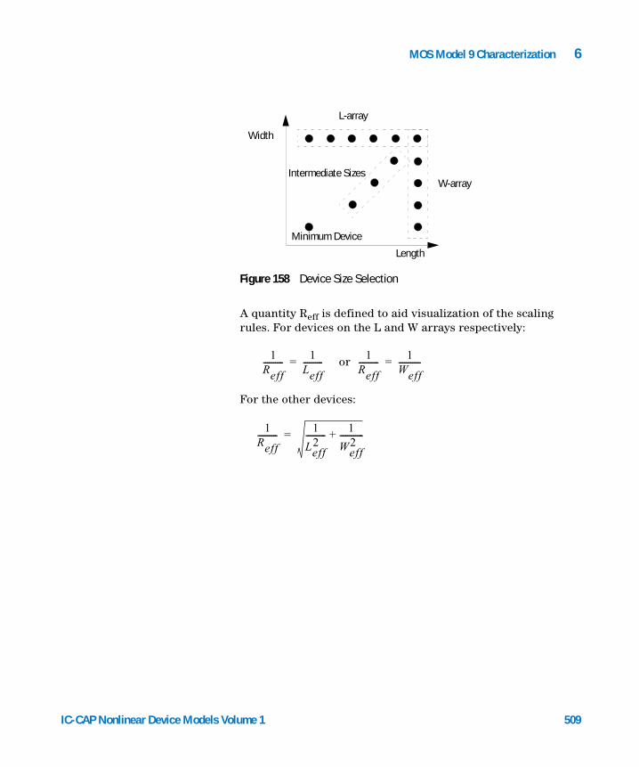
MOS Model 9 Characterization 6
IC-CAP Nonlinear Device Models Vo
A quantity Reff is defined to aid visualization of the scaling rules. For devices on the L and W arrays respectively:
or
For the other devices:
Figure 158 Device Size Selection
Width
Length
L-array
W-array
Minimum Device
Intermediate Sizes
1Reff----------
1Leff----------=
1Reff----------
1Weff-----------=
1Reff----------
1
Leff2
----------1
Weff2
------------+=
lu
me 1 509
6 MOS Model 9 Characterization
Optimizing
510
The steps below represent the basic maxiset optimization sequence.
1 Linear Ids − Vgs data
Vsb=0V: Optimize VTOR, SLVTO, SL2VTO, SWVTO, BETSQ, THE1R, SLTHE1R, and SWTHE1.
Varying Vsb: Optimize KOR, SLKO, SWKO, (KR, SLK, SWK, VSBXR, SLVSBX, SWVSBX), THE2R, SLTHE2R, and SWTHE2.
2 Subthreshold Ids − Vgs data
Vsb = 0V: Optimize GAMOOR, SLGAMOO, MOR, SLMO, ZET1R, and SLZET1.
3 Saturation gds − Vds data
Vsb = 0V: Optimize GAM1R, SLGAM1, SWGAM1, ALPR, SLALP, SWALP, and VPR.
4 Saturation Ids − Vds data
Vsb = 0V: Optimize THE3R, SLTHE3R, and SWTHE3.
5 Substrate current (Isub − Vgs) data
Vsb = 0V: Optimize A1R, SLA1, SWA1, A2R, SLA2, SWA2, A3R, SLA3, and SWA3.
6 Subthreshold Ids − Vgs data
Varying Vsb: Optimize VSBTR and SLVSBT.
Optimization Transforms and Macros
The transforms described in this section are available with the DUT extract.
full_extract
IC-CAP Nonlinear Device Models Volume 1
MOS Model 9 Characterization 6
IC-CAP Nonlinear Device Models Vo
The full_extract transform controls the optimization sequence for miniset extraction. It can be found under the setup single_ext.
1 Initialize parameters (par_init)
2 Linear region fitting at Vbs = 0 (lin_opt1)
3 Linear region fitting at all Vbs (lin_opt2 for 2 k-factor model) or (lin_opt3 for 1 k-factor model)
4 Subthreshold fitting at Vbs = 0 (subvt_opt1)
5 Gds fitting at Vbs = 0 (normal_gds_opt1 for most devices) or (large_gds_opt1 for the large device)
6 Ids fitting for Vbs = 0 (ids_opt1)
7 Avalanche fitting for Vbs = 0 (isub_opt1)
8 Repeat steps 2 through 7
9 Subthreshold fitting for all Vbs (subvt_opt2)
sca_opt
The sca_opt transform controls the optimization sequence for maxiset extraction. It can be found under the setup scaled_ext.
1 Linear region fitting at Vbs = 0 (sca_lin_opt1)
2 Linear region fitting for all Vbs (sca_lin_opt2 for the 2 k-factor option) or (sca_lin_opt3 for the 1 k-factor option)
3 Subthreshold fitting at Vbs = 0 (sca_subvt_opt1)
4 Gds fitting at Vbs = 0 (sca_gds_opt1)
5 Ids fitting at Vbs = 0 (sca_ids_opt1)
6 Avalanche current fitting at Vbs = 0 (sca_isub_opt1)
7 Subthreshold fitting for all Vbs (sca_subvt_opt2)
single_temp_opt
The single_temp_opt transform controls the optimization sequence for the temperature-dependent parameters at a single non-nominal temperature. It can be found under the setup single_temp_extract.
1 Initialize variables (temp_par_init)
2 Linear fitting at Vbs = 0 (single_temp_lin_opt1)
lume 1 511
512
6 MOS Model 9 Characterization
3 Linear fitting at all Vbs (single_tep_lin_opt2)
4 Subthreshold fitting at Vbs = 0 (single_temp_subvt_opt1)
5 Ids fitting at Vbs = 0 (single_temp_ids_opt1)
6 Avalanche current fitting at Vbs = 0 (single_temp_isub_opt1)
optimize_temperature_coefficients
The optimize_temperature_coefficients macro controls the optimization sequence for the temperature coefficients by calling the transforms listed below (found under the all_temp_extract setup) in the order shown.
1 all_temp_lin_opt1
2 all_temp_lin_opt2
3 all_temp_subvt_opt1
4 all_temp_ids_opt1
5 all_temp_isub_opt1
IC-CAP Nonlinear Device Models Volume 1
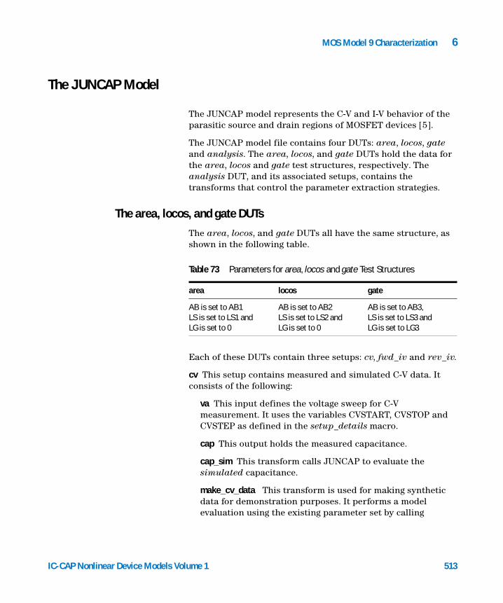
MOS Model 9 Characterization 6
The JUNCAP Model
IC-CAP Nonlinear Device Models Vo
The JUNCAP model represents the C-V and I-V behavior of the parasitic source and drain regions of MOSFET devices [5].
The JUNCAP model file contains four DUTs: area, locos, gate and analysis. The area, locos, and gate DUTs hold the data for the area, locos and gate test structures, respectively. The analysis DUT, and its associated setups, contains the transforms that control the parameter extraction strategies.
The area, locos, and gate DUTs
The area, locos, and gate DUTs all have the same structure, as shown in the following table.
Each of these DUTs contain three setups: cv, fwd_iv and rev_iv.
cv This setup contains measured and simulated C-V data. It consists of the following:
va This input defines the voltage sweep for C-V measurement. It uses the variables CVSTART, CVSTOP and CVSTEP as defined in the setup_details macro.
cap This output holds the measured capacitance.
cap_sim This transform calls JUNCAP to evaluate the simulated capacitance.
make_cv_data This transform is used for making synthetic data for demonstration purposes. It performs a model evaluation using the existing parameter set by calling
Table 73 Parameters for area, locos and gate Test Structures
area locos gate
AB is set to AB1LS is set to LS1 andLG is set to 0
AB is set to AB2LS is set to LS2 andLG is set to 0
AB is set to AB3,LS is set to LS3 andLG is set to LG3
lume 1 513
514
6 MOS Model 9 Characterization
cap_sim and then copies the resulting simulated data into the m part of the cap output. This macro assumes that the MOS Model 9 function MM9_COPY is available.
connect_cv Modify this transform to enable automatic connection to the area DUT for C-V measurements.
cv_plot This is a plot definition showing measured and simulated C-V data.
fwd_iv This setup contains the measured and simulated forward I-V data. It consists of the following:
va, vk These inputs define the anode and cathode voltages for forward I-V measurements. The variables FIVSTART, FIVSTOP and FIVSTEP control the voltage sweeps.
id The output current
id_sim A call to JUNCAP to evaluate the simulated current
make_iv_data A transform to make synthetic forward I-V data. The function MM9_COPY is used in this transform.
connect_fiv Modify this transform to enable automatic connection to the DUT for forward I-V measurements.
fwd_ivplot The plot definition for the forward I-V data
rev_iv This setup contains the measured and simulated reverse I-V data. It consists of the following:
va, vk These inputs define the anode and cathode voltages for reverse I-V measurements. The variables RIVSTART, RIVSTOP and RIVSTEP control the voltage sweeps.
id The output current
id_sim A call to JUNCAP to evaluate the simulated current
set_temp This transform sets the setup level variable TEMP to the model level variable TREVERSE. The reverse data may be measured at a different temperature, TREVERSE, than the forward I-V or C-V data. However, the JUNCAP function looks for a variable TEMP to determine the device temperature. Therefore TEMP is defined as a setup level variable in the
IC-CAP Nonlinear Device Models Volume 1
MOS Model 9 Characterization 6
IC-CAP Nonlinear Device Models Vo
area/rev_iv, locos/rev_iv, gate/rev_iv and analysis/rev_iv setups. Thus, during simulations in these setups, the setup variable TEMP will supersede the model level variable TEMP.
make_iv_data A transform to make synthetic reverse I-V data. The function MM9_COPY is used is this transform.
connect_riv You can modify this transform to enable automatic connection to the DUT for reverse I-V measurements.
rev_ivplot The plot definition for the reverse I-V data.
The analysis DUT
In the analysis DUT, the dimensions AB, LS and LG are set to unity. The setups are cv, fwd_iv and rev_iv.
cv This setup controls the extraction of the C-V parameters and contains the following:
va This input definition for the anode voltage is the same as that in the area/cv, locos/cv and gate/cv setups.
cjbvn A transform that extracts (and holds) the normalized area sub-region contribution to capacitance from the measurements in the area/cv, locos/cv and gate/cv setups.
set_cjbr A transform that makes an initial approximation to the parameter CJBR by setting it to the value of cjbvn at the point where the anode voltage is closest to zero.
cjbvn_sim A transform that calls JUNCAP to evaluate the area sub-region component of capacitance.
fit_cjbvn An optimization definition that causes the parameters CJBR, PB and VDBR to be optimized with respect to the normalized area sub-region capacitance. The parameter limits are controlled by the following model variables, which you can change in the model variables table:
CJBR_MIN CJBR_MAX PB_MIN
PB_MAX VDBR_MIN VDBR_MAX
lume 1 515
516
6 MOS Model 9 Characterization
The data limits are controlled by the following variables, which are also in the model variables table:
cjsvn A transform that extracts (and holds) the normalized locos sub-region contribution to capacitance from the measurements in the area/cv, locos/cv and gate/cv setups.
set_cjsr A transform that makes an initial approximation to the parameter CJSR by setting it to the value of cjsvn at the point where the anode voltage is closest to zero.
cjsvn_sim A transform that calls JUNCAP to evaluate the locos sub-region component of capacitance
fit_cjsvn An optimization definition that causes the parameters CJSR, PS and VDSR to be optimized with respect to the normalized locos sub-region capacitance. The parameter limits are controlled by the following model variables, which you can change in the model variables table.
The data limits are controlled by the variables, which are also in the model variables table.
cjgvn A transform that extracts (and holds) the normalized gate sub-region contribution to capacitance from the measurements in the area/cv, locos/cv and gate/cv setups.
set_cjgr A transform that makes an initial approximation to the parameter CJGR by setting it to the value of cjgvn at the point where the anode voltage is closest to zero.
cjgvn_sim A transform that calls JUNCAP to evaluate the gate sub-region component of capacitance
CV_VMIN CV_VMAX
CJSR_MIN CJSR_MAX PS_MIN
PS_MAX VDSR_MIN VDSR_MAX
CV_VMIN CV_VMAX
IC-CAP Nonlinear Device Models Volume 1
MOS Model 9 Characterization 6
IC-CAP Nonlinear Device Models Vo
fit_cjgvn An optimization definition that causes the parameters CJGR, PG and VDGR to be optimized with respect to the normalized gate sub-region capacitance. The parameter limits are controlled by the following model variables, which you can change in the model variables table.
The data limits are controlled by the following variables, which are also in the model variables table:
init_cv_pars A transform to initialize some of the C-V parameters before optimization begins. The parameters initialized are:
VDBR = VDSR = VDGR = 0.75
PB = PS = PG = 0.4
opt_all_cv An optimization definition that causes all the C-V parameters to be optimized with respect to the measured data in the area/cv, locos/cv and gate/cv setups. The parameters optimized are:
The parameter limits are controlled by the following model variables:
CJGR_MIN CJGR_MAX PG_MIN
PG_MAX VDGR_MIN VDGR_MAX
CV_VMIN CV_VMAX
CJBR CJSR CJGR
VDBR VDSR VDGR
PB PS PG
CJBR_MIN CJBR_MAX CJSR_MIN CJSR_MAX CJGR_MIN
CJGR_MAX VDBR_MIN VDBR_MAX VDSR_MIN VDSR_MAX
VDGR_MIN VDGR_MAX PB_MIN PB_MAX PS_MIN
lume 1 517

518
6 MOS Model 9 Characterization
The data limits are controlled by the following variables:
set_unit_dimensions A transform that sets the dimensions AB, LS and LG in the analysis DUT to unity.
update_cv_curves A transform that resimulates all the C-V curves in the area/cv, locos/cv, gate/cv and analysis/cv setups.
cjb A plot definition for the normalized area sub-region contribution to capacitance.
cjs A plot definition for the normalized locos sub-region contribution to capacitance.
cjs A plot definition for the normalized gate sub-region contribution to capacitance.
fwd_iv This setup controls the extraction of the I-V parameters with respect to the forward I-V data. In the forward region at moderate and high applied voltages the diffusion current components dominate. However for low-applied voltages the generation components are also important. Therefore all the optimizations to the forward I-V curves target both the diffusion and generation parameters.
va, vk These input definitions for the anode and cathode voltages are the same as those in the area/fwd_iv, locos/fwd_iv and gate/fwd_iv setups.
ibn A transform that extracts (and holds) the normalized area sub-region contribution to forward current from the measurements in the area/fwd_iv, locos/fwd_iv and gate/fwd_iv setups.
ibn_sim A transform that calls JUNCAP to evaluate the area sub-region component of current.
PS_MAX PG_MIN PG_MAX
CV_VMIN CV_VMAX
IC-CAP Nonlinear Device Models Volume 1
MOS Model 9 Characterization 6
IC-CAP Nonlinear Device Models Vo
fit_ibn An optimization definition that causes the parameters JSDBR, NB and JSGBR to be optimized with respect to the normalized area sub-region forward current. The parameter limits are controlled by the model variables, which you can change in the model variables table.
The data limits are controlled by the following variables, which are also in the model variables table.
isn A transform that extracts (and holds) the normalized locos sub-region contribution to forward current from the measurements in the area/fwd_iv, locos/fwd_iv and gate/fwd_iv setups.
isn_sim A transform that calls JUNCAP to evaluate the locos sub-region component of current.
fit_isn An optimization definition that causes the parameters JSDSR, NS and JSGSR to be optimized with respect to the normalized locos sub-region forward current. The parameter limits are controlled by the following model variables, which you can change in the model variables table.
The data limits are controlled by the following variables, which are also in the model variables table:
JSDBR_MIN JSDBR_MAX NB_MIN
NB_MAX JSGBR_MIN JSGBR_MAX
FIV_VMIN FIV_VMAX
JSDSR_MIN JSDSR_MAX NS_MIN
NS_MAX JSGSR_MIN JSGSR_MAX
FIV_VMIN FIV_VMAX
lume 1 519
520
6 MOS Model 9 Characterization
ign A transform that extracts (and holds) the normalized gate sub-region contribution to forward current from the measurements in the area/fwd_iv, locos/fwd_iv and gate/fwd_iv setups.
ign_sim A transform that calls JUNCAP to evaluate the gate sub-region component of current.
fit_ign An optimization definition that causes the parameters JSDGR, NG and JSGGR to be optimized with respect to the normalized gate sub-region forward current. The parameter limits are controlled by the following model variables, which you can change in the model variables table:
The data limits are controlled by the following variables, which are also in the model variables table.
init_iv_pars A transform to initialize some of the I-V parameters before optimization begins. The parameters initialized are:
opt_all_fwd_iv An optimization definition that causes all the I-V parameters to be optimized with respect to the measured data in the area/fwd_iv, locos/fwd_iv and gate/fwd_iv setups. The parameters optimized are:
JSDGR_MIN JSDGR_MAX NG_MIN
NG_MAX JSGGR_MIN JSGGR_MAX
FIV_VMIN FIV_VMAX
JSDBR = 10n JSDSR = JSDGR = 10f NB = NS = NG = 1
JSGBR = 1u JSGSR = JSGGR = 100p
JSDBR JSDSR JSDGR NB NS
NG JSGBR JSGSR JSGGR
IC-CAP Nonlinear Device Models Volume 1
MOS Model 9 Characterization 6
IC-CAP Nonlinear Device Models Vo
The parameter limits are controlled by the following model variables:
The data limits are controlled by the variables:
update_iv_curves A transform that resimulates all the I-V curves in the following setups:
ib A plot definition for the normalized area sub-region contribution to current
is A plot definition for the normalized locos sub-region contribution to current
ig A plot definition for the normalized gate sub-region contribution to current
rev_iv This setup controls the extraction of the I-V parameters with respect to the reverse I-V data. Current in the reverse region is dominated by the generation effects and so only the generation parameters are considered during these extractions.
JSDBR_MIN JSDBR_MAX JSDSR_MIN JSDSR_MAX
JSDGR_MIN JSDGR_MAX NB_MIN NB_MAX
NS_MIN NS_MAX NG_MIN NG_MAX
JSGBR_MIN JSGBR_MAX JSGSR_MIN JSGSR_MAX,
JSGGR_MIN JSGGR_MAX
FIV_VMIN FIV_VMAX
area fwd_iv, rev_iv
locos fwd_iv, rev_iv
gate fwd_iv, rev_iv
analysis fwd_iv, rev_iv
lume 1 521

522
6 MOS Model 9 Characterization
va, vk These input definitions for the anode and cathode voltages are the same as those in the area/rev_iv, locos/rev_iv and gate/rev_iv setups.
ibn A transform that extracts (and holds) the normalized area sub-region contribution to reverse current from the measurements in the area/rev_iv, locos/rev_iv and gate/rev_iv setups.
ibn_sim A transform that calls JUNCAP to evaluate the area sub-region component of current.
fit_ibn An optimization definition that causes the parameter JSGBR to be optimized with respect to the normalized area sub-region reverse current. The parameter limits are controlled by the following model variables, which you can change in the model variables table.
The data limits are controlled by the following variables, which are also in the model variables table.
isn A transform that extracts (and holds) the normalized locos sub-region contribution to reverse current from the measurements in the area/rev_iv, locos/rev_iv and gate/rev_iv setups.
isn_sim A transform that calls JUNCAP to evaluate the locos sub-region component of current.
fit_isn An optimization definition that causes the parameter JSGSR to be optimized with respect to the normalized locos sub-region reverse current. The parameter limits are controlled by the following model variables, which you can change in the model variables table.
JSGBR_MIN JSGBR_MAX
RIV_VMIN RIV_VMAX
JSGSR_MIN JSGSR_MAX
IC-CAP Nonlinear Device Models Volume 1
MOS Model 9 Characterization 6
IC-CAP Nonlinear Device Models Vo
The data limits are controlled by the following variables, which are also in the model variables table.
ign A transform that extracts (and holds) the normalized gate sub-region contribution to reverse current from the measurements in the area/rev_iv, locos/rev_iv and gate/rev_iv setups.
ign_sim A transform that calls JUNCAP to evaluate the gate sub-region component of current.
fit_ign An optimization definition that causes the parameter JSGGR to be optimized with respect to the normalized gate sub-region reverse current. The parameter limits are controlled by the following model variables, which you can change in the model variables table.
The data limits are controlled by the following variables, which are also in the model variables table.
set_temp This transform sets the setup level variable TEMP to the model level variable TREVERSE.
opt_all_rev_iv An optimization definition that causes all the generation parameters to be optimized with respect to the measured data in the area/rev_iv, locos/rev_iv and gate/rev_iv setups. The parameters optimized are:
The parameter limits are controlled by the following model variables:
RIV_VMIN RIV_VMAX
JSGGR_MIN JSGGR_MAX
RIV_VMIN RIV_VMAX
JSGBR JSGSR JSGGR
lume 1 523
524
6 MOS Model 9 Characterization
The data limits are controlled by the following variables:
ib A plot definition for the normalized area sub-region contribution to current.
is A plot definition for the normalized locos sub-region contribution to current.
ig A plot definition for the normalized gate sub-region contribution to current.
JSGBR_MIN JSGBR_MAX JSGSR_MIN
JSGSR_MAX JSGGR_MIN JSGGR_MAX
FIV_VMIN FIV_VMAX
Macros
This section describes the macros provided with the JUNCAP model.
setup_details This macro prompts you for various setup details. These details are stored in the model variables table. The current values of the variables are used as prompts so you can easily change one setting by executing the macro a second time and choosing OK to all questions except the change required. The information requested by this macro is as follows:
TR Model parameter representing reference temperature
VR Model parameter representing the reference voltage for parameter scaling (usually 0)
TEMP Ambient temperature at which the forward I-V and the C-V curves will be measured
TREVERSE The temperature at which the reverse I-V curves will be measured. If possible, this should be higher than TEMP to accentuate the current component from generation effects
AB1 The area of the area DUT
LS1 The locos perimeter length of the area DUT
IC-CAP Nonlinear Device Models Volume 1
MOS Model 9 Characterization 6
IC-CAP Nonlinear Device Models Vo
The setup_details macro also calls the transform set_unit_dimensions, which sets the dimensions in the analysis DUT to unity.measure_cv This macro causes a measurement to be taken in the cv setups of the area, locos and gate DUTs. At the end of these measurements, you are prompted to specify the following information:
AB2 The area of the locos DUT
LS2 The locos perimeter length of the locos DUT
AB3 The area of the gate DUT
LS3 The locos perimeter length of the gate DUT
LG3 The gate perimeter length of the gate DUT
CONNECT_CV This variable is set depending on whether the user wishes to use manual or automatic connections for C-V measurement.
CONNECT_FIV This variable is set depending on whether the user wishes to use manual or automatic connections for forward I-V measurement.
CONNECT_RIV This variable is set depending on whether the user wishes to use manual or automatic connections for reverse I-V measurement.
CVSTART The start voltage for C-V sweeps
CVSTOP The stop voltage for C-V sweeps
CVSTEP The voltage step for C-V sweeps
FIVSTART The start voltage for forward I-V sweeps
FIVSTOP The stop voltage for forward I-V sweeps
FIVSTEP The voltage step for forward I-V sweeps
RIVSTART The start voltage for reverse I-V sweeps
RIVSTOP The stop voltage for reverse I-V sweeps
RIVSTEP The voltage step for reverse I-V sweeps
DATASOURCE If set to M, measurements will be taken. Otherwise data will be generated from simulations
DISPLAYPLOTS If set to Y, plots are displayed during measurement and optimizations. Otherwise they are not (unless they have previously been displayed and not closed).
lume 1 525
526
6 MOS Model 9 Characterization
measure_forward_iv This macro causes a measurement to be taken in the fwd_iv setups of the area, locos and gate DUTs. At the end of these measurements. you are prompted to specify the following information:
measure_reverse_iv This macro causes a measurement to be taken in the rev_iv setups of the area, locos and gate DUTs. At the end of these measurements, you are prompted to specify the following information:
extract_cv_pars This macro controls the extraction of the C-V parameters by splitting the C-V data into the area, locos and gate contributions and optimizing the parameters to these. At the end of the extractions, the simulated C-V arrays in the area, locos, gate and analysis DUTS are updated with the new parameters.
extract_fwd_iv_pars This macro controls the extraction of the forward I-V parameters by splitting the forward I-V data into the area, locos and gate contributions and optimizing the parameters to these. At the end of the extractions, the simulated I-V arrays (forward and reverse) in the area, locos, gate and analysis DUTS are updated with the new parameters.
CV_VMI The lower voltage limit for optimizations with respect to the C-V data
CV_VMAX The upper voltage limit for optimizations with respect to the C-V data
FIV_VMIN The lower voltage limit for optimizations with respect to the forward I-V data
FIV_VMAX The upper voltage limit for optimizations with respect to the forward I-V data
RIV_VMIN The lower voltage limit for optimizations with respect to the reverse I-V data
RIV_VMAX The upper voltage limit for optimizations with respect to the reverse I-V data
IC-CAP Nonlinear Device Models Volume 1
MOS Model 9 Characterization 6
IC-CAP Nonlinear Device Models Vo
extract_rev_iv_pars This macro controls the extraction of the reverse I-V parameters by splitting the reverse I-V data into the area, locos and gate contributions and optimizing the parameters to these. At the end of the extractions, the simulated I-V arrays (forward and reverse) in the area, locos, gate and analysis DUTS are updated with the new parameters.
opt_all_cv This macro controls the optimization of the full set of C-V parameters with respect to the measured data in the area, locos and gate DUTs. At the end of the extractions, the simulated C-V arrays in the area, locos, gate and analysis DUTS are updated with the new parameters.
opt_all_fwd_iv This macro controls the optimization of the full set of I-V parameters with respect to the measured forward I-V data in the area, locos and gate DUTs. At the end of the extractions, the simulated I-V arrays (forward and reverse) in the area, locos, gate and analysis DUTS are updated with the new parameters.
opt_all_rev_iv This macro controls the optimization of the generation current parameters with respect to the measured reverse I-V data in the area, locos and gate DUTs. At the end of the extractions, the simulated I-V arrays (forward and reverse) in the area, locos, gate and analysis DUTS are updated with the new parameters.
simulate_all_curves This macro allows all the curves to be resimulated.
set_new_TR This macro allows the model parameters to be recalculated for a new reference temperature.
read_data_from_directory Reads data previously stored in a subdirectory under the current working directory.
write_data_to_directory Writes the data to a subdirectory under the current working directory.
General Extraction Methodology
The JUNCAP model extraction methodology assumes that the parasitic source and drain regions consist of three sub-regions:
• The area of the source/drain
lume 1 527
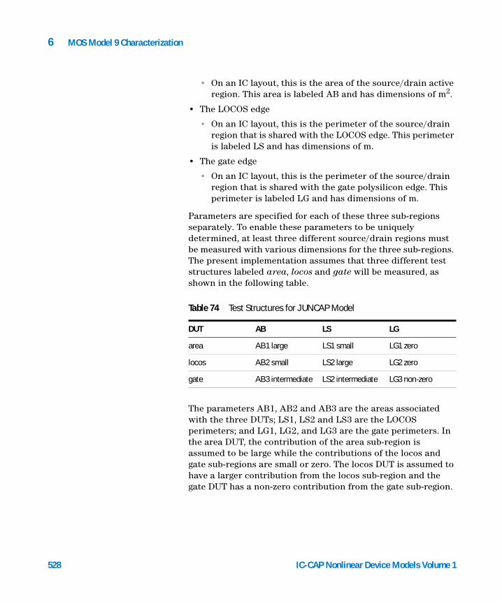
528
6 MOS Model 9 Characterization
• On an IC layout, this is the area of the source/drain active region. This area is labeled AB and has dimensions of m2.
• The LOCOS edge
• On an IC layout, this is the perimeter of the source/drain region that is shared with the LOCOS edge. This perimeter is labeled LS and has dimensions of m.
• The gate edge
• On an IC layout, this is the perimeter of the source/drain region that is shared with the gate polysilicon edge. This perimeter is labeled LG and has dimensions of m.
Parameters are specified for each of these three sub-regions separately. To enable these parameters to be uniquely determined, at least three different source/drain regions must be measured with various dimensions for the three sub-regions. The present implementation assumes that three different test structures labeled area, locos and gate will be measured, as shown in the following table.
The parameters AB1, AB2 and AB3 are the areas associated with the three DUTs; LS1, LS2 and LS3 are the LOCOS perimeters; and LG1, LG2, and LG3 are the gate perimeters. In the area DUT, the contribution of the area sub-region is assumed to be large while the contributions of the locos and gate sub-regions are small or zero. The locos DUT is assumed to have a larger contribution from the locos sub-region and the gate DUT has a non-zero contribution from the gate sub-region.
Table 74 Test Structures for JUNCAP Model
DUT AB LS LG
area AB1 large LS1 small LG1 zero
locos AB2 small LS2 large LG2 zero
gate AB3 intermediate LS2 intermediate LG3 non-zero
IC-CAP Nonlinear Device Models Volume 1
MOS Model 9 Characterization 6
IC-CAP Nonlinear Device Models Vo
The capacitance associated with any DUT is considered to be the sum of the contributions of the three sub-regions. For example, for the DUT gate, the capacitance at any voltage V is given by:
C(V) = C_AREA(V).AB3 + C_LOCOS(V).LS3 + C_GATE(V).LG3
where C_AREA(V),C_LOCOS(V) and C_GATE(V) are the normalized contributions of the area, locos and gate sub-regions at voltage V.
With respect to current, JUNCAP includes two mechanisms: diffusion and generation. These are described separately for each sub-region so that for the DUT gate, the current flow at any voltage V is given by:
I(V) = ( ID_AREA(V) + IG_AREA(V) ).AB3
+ ( ID_LOCOS(V) + IG_LOCOS(V) ).AL3
+ ( ID_GATE(V) + IG_GATE(V) ).AG3
where ID_AREA(V) and IR_AREA(V) are the normalized contributions of the diffusion current and generation current, respectively, for the area sub-region at voltage V with similar notation being used for the locos and gate sub-regions.
Once the three DUTs have been measured, a set of simultaneous equations can be solved that allows the contributions of the area, locos and gate sub-regions to be separated and normalized. Parameter extraction then proceeds by optimizing the relevant parameters to each of the sub-region contributions in turn. Finally, the model parameters may be fine-tuned by optimization with respect to the directly-measured data in the area, locos and gate DUTs.
For the case of a well diode, you should specify that there is no gate test structure by setting the variable AB3 to zero. With AB3=0, the gate device will be ignored during measurements and optimizations.
lume 1 529
6 MOS Model 9 Characterization
References
530
1 “Compact MOS modeling for analog circuit simulation” (IEDM '93)
2 “The high-frequency analogue performance of MOSFETs” (IEDM '94)
3 “Circuit Sensitivity Analysis in Terms of Process Parameters” (SISDEP '95)
4 Unclassified report, NL-UR 003/94, R.M.D.A. Velghe, D.B.M. Klaassen, F. M. Klaassen, Philips Research Laboratories, June, 1995
5 Unclassified report, NL-UR 028/95, R.M.D.A. Velghe
IC-CAP Nonlinear Device Models Volume 1
Agilent 85190A IC-CAP 2008Nonlinear Device Models Volume 1
7UCB MOS Level 2 and 3 Characterization
UCB MOSFET Model 533
Simulators 534
MOSFET Model Parameters 535
Test Instruments 541
Measuring and Extracting 543
Extraction Algorithms 553
HSPICE LEVEL 6 MOSFET Model 556
References 560
This chapter describes the UC Berkeley MOSFET transistor model supported in SPICE. Descriptions of model setup, instrument connections, and model parameters are included as well as test instrument information. Information is included for making DC and capacitance measurements and their corresponding extractions.
NOTE The HSPICE LEVEL 6 MOSFET model is an enhanced version of the MOSFET LEVEL 2 model; refer to the section “HSPICE LEVEL 6 MOSFET Model” on page 556 for parameter measurement and extraction information.
The IC-CAP MOSFET modeling module provides setups that can be used for general measurement and model extraction for MOS devices. Four example files are provided for the MOSFET model; the files can also be used as a template for creating custom model configurations.
531Agilent Technologies
532
7 UCB MOS Level 2 and 3 Characterization
nmos2.mdl extracts parameters for the LEVEL 2 N-channel model
pmos2.mdl extracts parameters for the LEVEL 2 P-channel model
nmos3.mdl extracts parameters for the LEVEL 3 N-channel model
pmos3.mdl extracts parameters for the LEVEL 3 P-channel model
The IC-CAP system offers the flexibility to modify any measurement or simulation specification.
The model extractions provided are also intended for general MOS IC processes. If you have another method of extracting specific model parameters, you can do so with the Program function or by writing a function in C and linking it to the function list. For Program function details or for writing user-defined C-language routines, refer to Chapter 9, “Using Transforms and Functions,” in the IC-CAP User’s Guide.
IC-CAP Nonlinear Device Models Volume 1

UCB MOS Level 2 and 3 Characterization 7
UCB MOSFET Model
IC-CAP Nonlinear Device Models Vo
The UCB MOSFET model is fully compatible with the UCB model developed for use with the UCB SPICE simulator. The model is actually a combination of three models, each being specified by an appropriate value of the LEVEL parameter. After specifying the model, enter the correct set of parameters for that model. Some of these parameters are shared between different models, while others affect only a specific model.
Extraction for the LEVEL 1 model (Shichman-Hodges) is not supplied with this release of IC-CAP. The LEVEL 2 model [1] is an advanced version of LEVEL 1, and can use either electrical or process type parameters. The LEVEL 3 [1] model is semi-empirical because it uses parameters that are defined by curve fitting rather than by device physics.
lume 1 533
7 UCB MOS Level 2 and 3 Characterization
Simulators
534
The MOSFET model is supported by the SPICE simulators included with IC-CAP: SPICE2, SPICE3 and HPSPICE. The model files provided can also be used with the HSPICE simulator and, with some modification, the Saber simulator.
NOTE Simulators are provided as a courtesy to IC-CAP users; they are not supported by Agilent Technologies.
The default nominal temperature for HPSPICE is 25°C; for SPICE2 and SPICE3 it is 27°C. To force a nominal temperature, set the TNOM variable to the desired value.
IC-CAP Nonlinear Device Models Volume 1

UCB MOS Level 2 and 3 Characterization 7
MOSFET Model Parameters
IC-CAP Nonlinear Device Models Vo
The following table lists parameters for the three model levels according to DC and cv extraction in IC-CAP. (Some of these parameters are redundant and therefore only a subset of them is extracted in IC-CAP.) Table 76 describes model parameters by related categories and provide default values. The parameter values are displayed in the Circuit folder. Table 77 lists setup attributes.
Controlling Model Parameters
Table 75 Summary of UCB MOSFET
Type LEVEL 1 LEVEL 2† LEVEL 3†
Classical VTO, GAMMA, PHI KP IS, JS, TOX
NSUB, UO, UCRIT, UEXP, UTRA, NFS, NSS, TPG
NSUB, UO, THETA, NFS, NSS, TPG
Short-channel LD, XJ LD, XJ
Narrow-width DELTA, WD†††
Saturation LAMBDA NEFF, VMAX ETA, KAPPA
External resistance NRD††, NRS†† RD, RS
Junction capacitance AD††, AS††, CBD, CBS CJ, FC, MJ, PB
Sidewall capacitance PD††, PS††, CSJW, MJSW
Overlap capacitance CGBO, CGDO, CGSO
General LEVEL, L††, W††
IC-CAP Temperature Specification
TNOM (system variable)
Notes:† LEVEL 2 and LEVEL 3 also include LEVEL 1 parameters.†† Indicates device parameters (model and device parameters are listed together).††† WD does not exist in the SPICE UCB version; it has been added to some SPICE versions and is included in IC-CAP. If WD is not in your simulator, ignore the result (set to zero), or subtract 2⋅WD from the channel width. In the MOS model files provided with IC-CAP, the width specification W in each of the DUTs has been modified to subtract the value of 2⋅WD from the drawn width. WD is specified in Model Variables.
lume 1 535

536
7 UCB MOS Level 2 and 3 Characterization
Table 76 UCB MOSFET Parameters
Name Description Default
Capacitance
CGBO Gate to Bulk Overlap Capacitance. Capacitance due to design rules that require the gate be extended beyond the channel by some amount. Not voltage dependent. Total Cgb capacitance equals Cgbo times channel length.
0 F/m
CGDO Gate to Drain Overlap Capacitance. Capacitance due to the lateral diffusion of the drain in an Si gate MOSFET. Not voltage dependent. Total Gcd capacitance equals Cgdo times the channel width.
0 F/m
CGSO Gate to Source Overlap Capacitance. Capacitance due to the lateral diffusion of the source in an Si gate MOSFET. Not voltage dependent because it is not a junction capacitance. Total Cgs capacitance equals Cgso times channel width.
0 F/m
CJSW Zero Bias Junction Sidewall Capacitance. Models the nonlinear junction capacitance between the drain and the source junction sidewall. (Pd + Ps) * CJSW = total junction sidewall capacitance.
0 F/m
MJSW Grading Coefficient of Junction Sidewall. Models the grading coefficient for the junction sidewall capacitance.
0.33
PB Bulk Junction Potential. Models the built-in potential of the bulk-drain or bulk-source junctions. The default is usually adequate.
0.8 volt
FC Forward Bias Non-Ideal Junction Capacitance Coefficient. Models the point (FC * PB) at which junction capacitance makes the transition between forward and reverse bias.
0.5
Electrical Process
IS Substrate Junction Saturation Current. Helps model current flow through the bulk-source or bulk-drain junction.
1×10-16 Amp
JS Substrate Junction Saturation Current/m2. Js equals Is divided by the junction area. For example, Isd=Js*Ad where Ad is the drain area.
1×10⁻⁴ A/m2
RD Drain Ohmic Resistance. This parameter is geometry independent in SPICE and IC-CAP. In fact, it is inversely proportional to channel width.
0 Ohm
UCRIT Critical Field for Mobility Degradation. Used in level=2 model only. 1000 V ⋅ cm-1
UEXP Critical Field Exponent. Used in level=2 model only. 0
UO Surface Mobility at Low Gate Levels. Specifies mobility in level=2 and level=3 models. In the level=2 model, if Kp is UTRA
600 cm2/(V ⋅ S)
IC-CAP Nonlinear Device Models Volume 1
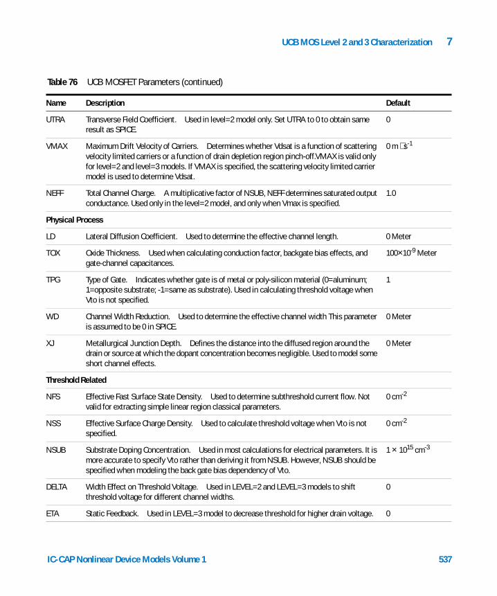
UCB MOS Level 2 and 3 Characterization 7
UTRA Transverse Field Coefficient. Used in level=2 model only. Set UTRA to 0 to obtain same result as SPICE.
0
VMAX Maximum Drift Velocity of Carriers. Determines whether Vdsat is a function of scattering velocity limited carriers or a function of drain depletion region pinch-off.VMAX is valid only for level=2 and level=3 models. If VMAX is specified, the scattering velocity limited carrier model is used to determine Vdsat.
0 m ⋅ s-1
NEFF Total Channel Charge. A multiplicative factor of NSUB, NEFF determines saturated output conductance. Used only in the level=2 model, and only when Vmax is specified.
1.0
Physical Process
LD Lateral Diffusion Coefficient. Used to determine the effective channel length. 0 Meter
TOX Oxide Thickness. Used when calculating conduction factor, backgate bias effects, and gate-channel capacitances.
100×10-9 Meter
TPG Type of Gate. Indicates whether gate is of metal or poly-silicon material (0=aluminum; 1=opposite substrate; -1=same as substrate). Used in calculating threshold voltage when Vto is not specified.
1
WD Channel Width Reduction. Used to determine the effective channel width This parameter is assumed to be 0 in SPICE.
0 Meter
XJ Metallurgical Junction Depth. Defines the distance into the diffused region around the drain or source at which the dopant concentration becomes negligible. Used to model some short channel effects.
0 Meter
Threshold Related
NFS Effective Fast Surface State Density. Used to determine subthreshold current flow. Not valid for extracting simple linear region classical parameters.
0 cm-2
NSS Effective Surface Charge Density. Used to calculate threshold voltage when Vto is not specified.
0 cm-2
NSUB Substrate Doping Concentration. Used in most calculations for electrical parameters. It is more accurate to specify Vto rather than deriving it from NSUB. However, NSUB should be specified when modeling the back gate bias dependency of Vto.
1 × 1015 cm-3
DELTA Width Effect on Threshold Voltage. Used in LEVEL=2 and LEVEL=3 models to shift threshold voltage for different channel widths.
0
ETA Static Feedback. Used in LEVEL=3 model to decrease threshold for higher drain voltage. 0
Table 76 UCB MOSFET Parameters (continued)
Name Description Default
IC-CAP Nonlinear Device Models Volume 1 537
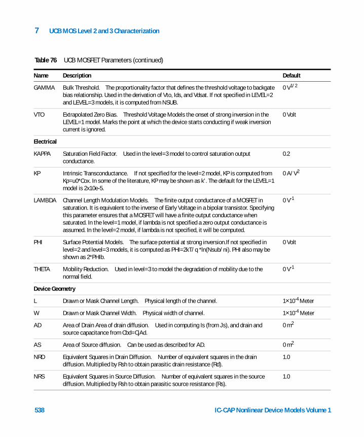
7 UCB MOS Level 2 and 3 Characterization
GAMMA Bulk Threshold. The proportionality factor that defines the threshold voltage to backgate bias relationship. Used in the derivation of Vto, Ids, and Vdsat. If not specified in LEVEL=2 and LEVEL=3 models, it is computed from NSUB.
0 V1/2
VTO Extrapolated Zero Bias. Threshold Voltage Models the onset of strong inversion in the LEVEL=1 model. Marks the point at which the device starts conducting if weak inversion current is ignored.
0 Volt
Electrical
KAPPA Saturation Field Factor. Used in the level=3 model to control saturation output conductance.
0.2
KP Intrinsic Transconductance. If not specified for the level=2 model, KP is computed from Kp=u0*Cox. In some of the literature, KP may be shown as k’. The default for the LEVEL=1 model is 2x10e-5.
0 A/V2
LAMBDA Channel Length Modulation Models. The finite output conductance of a MOSFET in saturation. It is equivalent to the inverse of Early Voltage in a bipolar transistor. Specifying this parameter ensures that a MOSFET will have a finite output conductance when saturated. In the level=1 model, if lambda is not specified a zero output conductance is assumed. In the level=2 model, if lambda is not specified, it will be computed.
0 V-1
PHI Surface Potential Models. The surface potential at strong inversion.If not specified in level=2 and level=3 models, it is computed as PHI=2kT/q *ln(Nsub/ni). PHI also may be shown as 2*PHIb.
0 Volt
THETA Mobility Reduction. Used in level=3 to model the degradation of mobility due to the normal field.
0 V-1
Device Geometry
L Drawn or Mask Channel Length. Physical length of the channel. 1×10⁻⁴ Meter
W Drawn or Mask Channel Width. Physical width of channel. 1×10⁻⁴ Meter
AD Area of Drain Area of drain diffusion. Used in computing Is (from Js), and drain and source capacitance from Cbd=CjAd.
0 m2
AS Area of Source diffusion. Can be used as described for AD. 0 m2
NRD Equivalent Squares in Drain Diffusion. Number of equivalent squares in the drain diffusion. Multiplied by Rsh to obtain parasitic drain resistance (Rd).
1.0
NRS Equivalent Squares in Source Diffusion. Number of equivalent squares in the source diffusion. Multiplied by Rsh to obtain parasitic source resistance (Rs).
1.0
Table 76 UCB MOSFET Parameters (continued)
Name Description Default
538 IC-CAP Nonlinear Device Models Volume 1
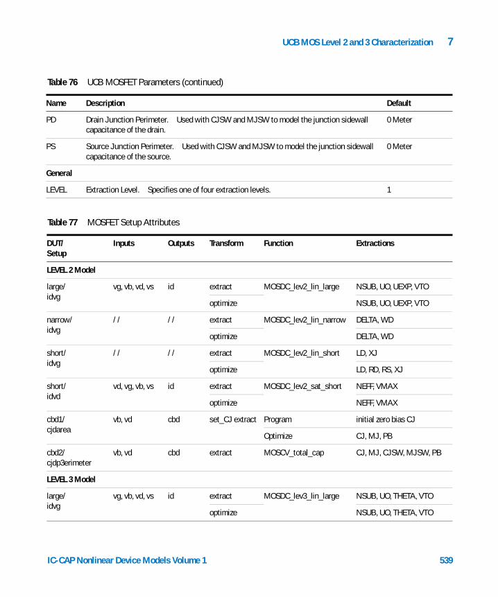
UCB MOS Level 2 and 3 Characterization 7
PD Drain Junction Perimeter. Used with CJSW and MJSW to model the junction sidewall capacitance of the drain.
0 Meter
PS Source Junction Perimeter. Used with CJSW and MJSW to model the junction sidewall capacitance of the source.
0 Meter
General
LEVEL Extraction Level. Specifies one of four extraction levels. 1
Table 77 MOSFET Setup Attributes
DUT/Setup
Inputs Outputs Transform Function Extractions
LEVEL 2 Model
large/idvg
vg, vb, vd, vs id extract MOSDC_lev2_lin_large NSUB, UO, UEXP, VTO
optimize NSUB, UO, UEXP, VTO
narrow/idvg
// // extract MOSDC_lev2_lin_narrow DELTA, WD
optimize DELTA, WD
short/idvg
// // extract MOSDC_lev2_lin_short LD, XJ
optimize LD, RD, RS, XJ
short/idvd
vd, vg, vb, vs id extract MOSDC_lev2_sat_short NEFF, VMAX
optimize NEFF, VMAX
cbd1/cjdarea
vb, vd cbd set_CJ extract Program initial zero bias CJ
Optimize CJ, MJ, PB
cbd2/cjdp3erimeter
vb, vd cbd extract MOSCV_total_cap CJ, MJ, CJSW, MJSW, PB
LEVEL 3 Model
large/idvg
vg, vb, vd, vs id extract MOSDC_lev3_lin_large NSUB, UO, THETA, VTO
optimize NSUB, UO, THETA, VTO
Table 76 UCB MOSFET Parameters (continued)
Name Description Default
IC-CAP Nonlinear Device Models Volume 1 539
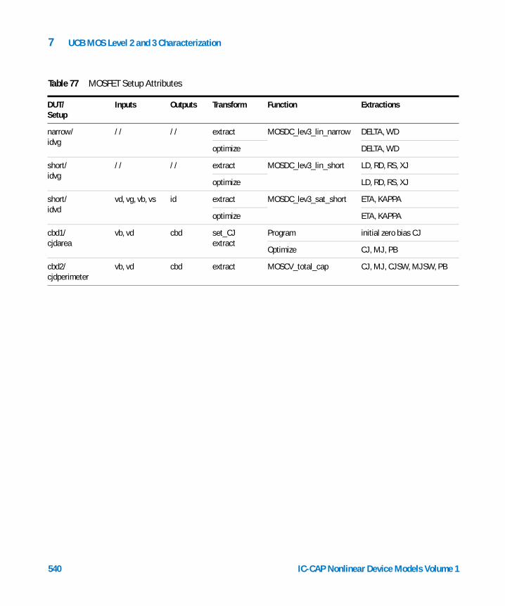
7 UCB MOS Level 2 and 3 Characterization
narrow/idvg
// // extract MOSDC_lev3_lin_narrow DELTA, WD
optimize DELTA, WD
short/idvg
// // extract MOSDC_lev3_lin_short LD, RD, RS, XJ
optimize LD, RD, RS, XJ
short/idvd
vd, vg, vb, vs id extract MOSDC_lev3_sat_short ETA, KAPPA
optimize ETA, KAPPA
cbd1/cjdarea
vb, vd cbd set_CJextract
Program initial zero bias CJ
Optimize CJ, MJ, PB
cbd2/cjdperimeter
vb, vd cbd extract MOSCV_total_cap CJ, MJ, CJSW, MJSW, PB
Table 77 MOSFET Setup Attributes
DUT/Setup
Inputs Outputs Transform Function Extractions
540 IC-CAP Nonlinear Device Models Volume 1
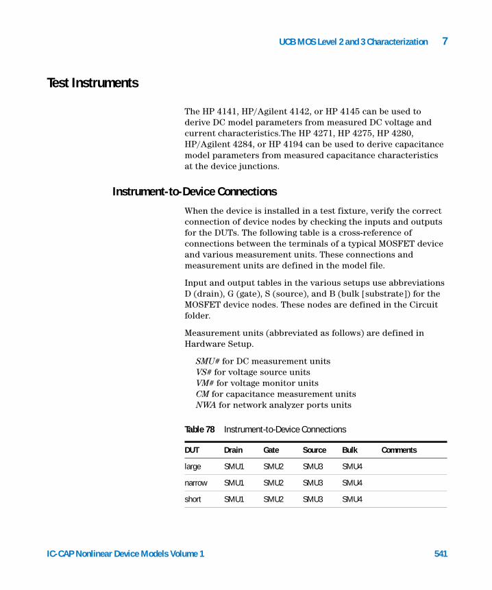
UCB MOS Level 2 and 3 Characterization 7
Test Instruments
IC-CAP Nonlinear Device Models Vo
The HP 4141, HP/Agilent 4142, or HP 4145 can be used to derive DC model parameters from measured DC voltage and current characteristics.The HP 4271, HP 4275, HP 4280, HP/Agilent 4284, or HP 4194 can be used to derive capacitance model parameters from measured capacitance characteristics at the device junctions.
Instrument-to-Device Connections
When the device is installed in a test fixture, verify the correct connection of device nodes by checking the inputs and outputs for the DUTs. The following table is a cross-reference of connections between the terminals of a typical MOSFET device and various measurement units. These connections and measurement units are defined in the model file.
Input and output tables in the various setups use abbreviations D (drain), G (gate), S (source), and B (bulk [substrate]) for the MOSFET device nodes. These nodes are defined in the Circuit folder.
Measurement units (abbreviated as follows) are defined in Hardware Setup.
SMU# for DC measurement unitsVS# for voltage source unitsVM# for voltage monitor unitsCM for capacitance measurement unitsNWA for network analyzer ports units
Table 78 Instrument-to-Device Connections
DUT Drain Gate Source Bulk Comments
large SMU1 SMU2 SMU3 SMU4
narrow SMU1 SMU2 SMU3 SMU4
short SMU1 SMU2 SMU3 SMU4
lume 1 541
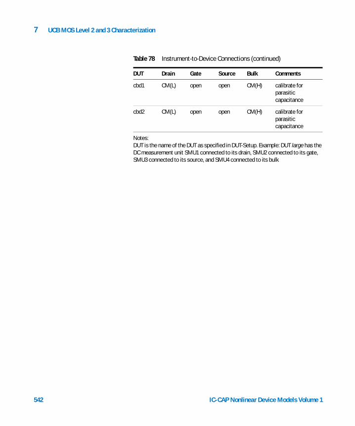
542
7 UCB MOS Level 2 and 3 Characterization
Notes:DUT is the name of the DUT as specified in DUT-Setup. Example: DUT large has the DC measurement unit SMU1 connected to its drain, SMU2 connected to its gate, SMU3 connected to its source, and SMU4 connected to its bulk
cbd1 CM(L) open open CM(H) calibrate for parasitic capacitance
cbd2 CM(L) open open CM(H) calibrate for parasitic capacitance
Table 78 Instrument-to-Device Connections (continued)
DUT Drain Gate Source Bulk Comments
IC-CAP Nonlinear Device Models Volume 1
UCB MOS Level 2 and 3 Characterization 7
Measuring and Extracting
IC-CAP Nonlinear Device Models Vo
This section provides guidelines as well as procedures for performing measurements and extractions of MOSFET devices.
Measurement and Extraction Guidelines
The following guidelines are provided to help you achieve more successful model measurements and extractions.
Setting Instrument Options
Before starting a measurement, you can quickly verify instrument options settings. Save the current instrument option settings by saving the model file to <file_name>.mdl from the model window. Some of the Instrument Options specify instrument calibration. For the most accurate results, calibrate the instruments before taking IC-CAP measurements.
Typical DC and cv instrument options are:
• DC measurements are generally taken with Integration Time = Medium.
• CV measurements in the femtofarad region usually require High Resolution = Yes and Measurement Freq (kHz) = 1000.
Measuring Instruments
Ensure that the measuring instruments (specified by unit names in the inputs and outputs) are correctly connected to the DUT. Refer to Table 78 for a list of nodes and corresponding measurement units. The quality of the measuring equipment (instruments, cables, test fixture, transistor sockets, and probes) can influence the noise level in the measurements and extracted parameter values.
For some measurements the instruments or test hardware must be calibrated to remove non-device parasitics from the DUT. For MOS devices, stray capacitance due to probe systems, bond pads, and so on should be calibrated out prior to each measurement.
lume 1 543
544
7 UCB MOS Level 2 and 3 Characterization
Extracting Model Parameters
For a given setup, you can find the extraction transforms in the Extract/Optimize folder. IC-CAP’s extraction algorithms exist as functions; choose Browse to list the functions available for a setup.
When the Extract command is selected from the setup, all extractions in the setup are performed in the order listed in the setup. This order is usually critical to proper extraction performance. Extractions are typically completed instantly and the newly extracted model parameter values are placed in Model Parameters.
Simulating Device Response
Simulation uses model parameter values currently in Model Parameters. A SPICE deck is created and the simulation performed. The output of the SPICE simulation is then read into IC-CAP as simulated data.
Select a simulator from Tools > Hardware Setup or define a SIMULATOR variable. DC simulations generally run much faster than cv simulations. CV simulations can be done in a much shorter time by executing the calc_mos_cbd_model transform instead of running the simulator.
If simulated results are not as expected, use the Simulation Debugger (Tools menu) to examine the input and output simulation files. The output of manual simulations is not available for further processing by IC-CAP functions (such as transforms and plots). For more information refer to “Using the Simulation Debugger" in the IC-CAP User’s Guide.
Displaying Plots
The Display Plot function displays all graphical plots defined in a setup. The currently active graphs are listed in the Plots folder in each setup.
IC-CAP Nonlinear Device Models Volume 1

UCB MOS Level 2 and 3 Characterization 7
IC-CAP Nonlinear Device Models Vo
Measured data is displayed as a solid line; simulated data is displayed as a dashed or dotted line. After an extraction and subsequent simulation, view the plots for agreement between measured and simulated data. Plots are automatically updated each time a measurement or simulation is performed.
Optimizing Model Parameters
Optimization of model parameters improves the agreement between measured and simulated data. An optimize transform whose Extract Flag is set to Yes is automatically called after any extraction that precedes it in the transform list.
Extracting Parameters
This section describes the general procedure for extracting model parameter data from the UCB MOSFET transistor. The general procedure applies to all types of parameters; differences between extracting one type and another are primarily in the types of instruments, setups, and transforms used. Also included in this section is information specific to DC and capacitance measurements and extractions.
Parameters are extracted from measured data taken directly from instruments connected to the inputs and outputs of the DUT. Using the extracted parameters simulated data can be generated by the simulator. Once measured and simulated data have been obtained, each data set can be plotted and the resulting Plots visually compared in the Plot window.
IC-CAP also extracts model parameters from simulated data. This capability is useful for creating a set of model parameters from the parameters of another model (parameter conversion) or for testing the accuracy of the extraction.
The general extraction procedure is summarized next, starting with the measurement process.
1 Install the device to test in a test fixture and connect the test instruments.
2 Ensure the test fixture, signal source and measuring instruments, and workstation are physically and logically configured for the IC-CAP system.
lume 1 545
546
7 UCB MOS Level 2 and 3 Characterization
3 Load the model.
4 Select the DUT. In the DUT Parameters folder, enter the W and L device parameters for the selected DUT.
5 In the Macros folder, select the appropriate macro to enter the process parameters.
6 Select the setup.
7 Issue the Measure command.
8 Issue the Extract command.
9 Issue the Simulate command.
10 Display the results.
11 Fine tune the extracted parameters if needed by optimizing.
DC Measurement and Extraction
In DC parameter extraction, the extracted parameters are directly related to the geometries of the devices being tested. For a DUT to accurately extract DC model parameters, it must have the correct L (drawn or mask channel length) and W (drawn or mask channel width) device parameters. Before executing an extraction or simulation, edit each DUT to ensure the L and W parameters are correct.
Before starting the extraction, enter several process parameters. The most important of these is TOX. Determine TOX by reading the process information for the device, or by measuring the oxide capacitance; TOX is measured in meters. Enter its value directly in Model Parameters, or run the init_parameters macro. Also use the init_parameters macro to enter initial values for XJ, LD, and RS. These initial values can contribute to the accuracy of the extracted parameters. They are overwritten by new values when the XJ, LD, and RS are extracted during the extraction process.
Accurate results depend on the sequence of the extraction. Follow this DC extraction sequence.
IC-CAP Nonlinear Device Models Volume 1
UCB MOS Level 2 and 3 Characterization 7
IC-CAP Nonlinear Device Models Vo
• Extract the classical parameters from the large device. Because length and width effects are not critical for the device used in this step, the classical parameters can be extracted very accurately. These parameters are used for the remainder of the extractions.
• Extract parameters from a narrow device, in which length effects are not important but the width effect and width parameters are.
• Extract length parameters using a short channel device and the classical parameter data acquired in the first extraction. RS and RD parameters, which predominate in this device, are also extracted in this step.
• All of the parameters extracted are used to calculate the saturation parameters for the short channel device. The short channel device is used for this procedure because of the predominance of the saturation parameters.
Do all of the measurements, followed by all of the extractions, and finally, the simulations. Extraction usually provides a reasonable fit to the measured data, but you can optimize data to attain an increased level of accuracy. Execute the optimization after extracting the DC parameters for each setup.
To perform DC parameter measurements:
1 Choose File > Open > Examples. Select <filename>.mdl and choose OK. Open the model window.
When the model window appears you are ready to begin measurement and extraction operations.
NOTE P-channel and N-channel MOS extractions are handled the same. pmos2.mdl or pmos3.mdl files are used for P-channel extractions; nmos2.mdl and nmos3.mdl files are used for N-channel extractions.
2 Select the DUT large. Enter the values for L and W. To include the effect of WD, enter the following expression for W:
< value > − 2 ⋅ WD
lume 1 547
548
7 UCB MOS Level 2 and 3 Characterization
where value is the drawn width and WD is defined as a model variable.
3 In Macros, select init_parameters. Enter the values for TOX, XJ, LD, and RS. Default values can be used by simply choosing OK in each dialog box.
4 Select the idvg setup and issue the Measure command.
5 Repeat these steps for narrow/idvg, short/idvg, and short/idvd.
To perform DC parameter extractions:
1 Select large/idvg. Select the transform extract and execute the selection to extract the LEVEL 2 classical parameters.
2 Repeat this procedure for narrow/idvg, short/idvg, and short/idvd.
All DC model parameters have now been extracted and their values are listed in Model Parameters.
Notes on DC Parameter Extraction
These procedures assume that the large device is large enough to make small geometry effects irrelevant. This condition exists when the device geometries are much larger than LD and WD. For a typical process, 50*50 microns should be sufficient. To improve accuracy, enter the approximate values of LD and WD in Model Parameters so they can be taken into consideration in the first extraction step. A more accurate value for each is produced by the second and third extractions.
When a very large device is not available and you cannot enter LD and WD, try the following:
1 Use the largest available device for the large setup and execute all four steps of the DC extraction.
2 Repeat the extraction sequence starting with the first step (you do not need to re-enter the parameters). The previously extracted parameters (particularly LD and WD) are used as the initial values.
IC-CAP Nonlinear Device Models Volume 1
UCB MOS Level 2 and 3 Characterization 7
IC-CAP Nonlinear Device Models Vo
To extract DC parameters when only one size of device is available, extract model parameters using the following sequence. This sequence does not extract geometry-dependent parameters but does extract a subset of parameters to fully model that size device.
1 Perform the large/idvg extraction to obtain the classical parameters.
2 Perform the short/idvd extraction to obtain the saturation parameters.
Enter the same L and W device parameters for both DUTs. The model can be reconfigured so that it has only one DUT with two setups, one similar to idvg and one similar to idvd. Copy the setup from large/idvg and the setup from short/idvd (copy complete setups so the appropriate extraction and optimization functions are included).
If you cannot determine the L and W for a single geometry device (as might be the case with a packaged transistor), set estimated values. The actual values are less important than the ratio between them. An incorrect ratio of W/L results in extraction of an unreasonable value for UO. In general, the mobility parameter UO should be set between 200 and 800. Start the extraction after setting the ratio of L and W to 1, then change the ratio of L to W to scale back the extracted value of UO.
Capacitance Measurement and Extraction
Capacitance parameters can be extracted before or after the DC parameters. The extraction requires that two different DUTs be measured; model parameters are extracted from the second DUT.
The extraction in the cbd1/cjdarea setup requires a single geometry to be measured and produces the parameters CJ, MJ, and PB. The extraction uses a transform set_CJ to find the initial zero bias value of CJ then uses optimization to obtain all three parameter values.
lume 1 549

550
7 UCB MOS Level 2 and 3 Characterization
The extraction in the cbd2/cjdperimeter setup requires two geometries to be measured (one in the cbd1/cjdarea setup and one in the cbd2/cjdperimeter setup) that produces the parameters CJ, MJ, PB, CJSW, and MJSW—and therefore a more complete capacitance model.
The extract transform uses the MOSCV_total_cap function to simultaneously solve for the bottom area and sidewall capacitance parameters. To extract the capacitance contributions from the bottom area and the sidewall periphery the geometries must have different area-to-perimeter ratios. The device measured with the cbd1/cjdarea setup should have a high bottom area to perimeter area ratio and the device measured with the cbd2/cjdperimeter should have a low bottom area to perimeter area ratio.
Place the device to be measured into the test fixture. Ensure that the CMs (Capacitance Meters Units) connected to the device correspond to the same CMs in Table 78 for each of the next two measurements. Calibrate the capacitance meter before taking each measurement.
The extractions of the sidewall capacitance parameter sets use the measured data from both setups—measure both setups before performing the extraction.
1 In Macros, select init_cap_parameters and Execute.
2 Enter the drain area and perimeter information.
3 Connect the low terminal of the capacitance meter (CM low) to drain and connect the high terminal (CM high) to bulk.
4 Select cbd1/cjdarea and Measure to measure the first drain-bulk junction capacitance.
5 Repeat steps 3 and 4 for cbd2/cjdperimeter if both geometry sizes are being measured.
Perform the model parameter extractions.
1 If a single geometry was measured, select cbd1/cjdarea. If two different geometries were measured, select cbd2/cjdperimeter.
2 Choose Extract.
Optimization is usually not required for capacitance data.
IC-CAP Nonlinear Device Models Volume 1
UCB MOS Level 2 and 3 Characterization 7
IC-CAP Nonlinear Device Models Vo
Notes on Capacitance Parameter Extraction
The drain-to-substrate and source-to-substrate junction capacitances are modeled as a combination of the sidewall and bottom (area) capacitances. To extract the parameters for these capacitances, first measure capacitance against voltage on two different size capacitors. Then execute the extraction command using two setups: cjdarea and cjdperimeter. Execute cjdarea on a square-shaped capacitance with a small sidewall to bottom ratio, and cjdperimeter on a long, narrow junction with a large sidewall to bottom ratio.
Each p-n junction should be reverse-biased when measured. Extraction is performed by the MOSCV_total_cap function. The parameters CJ, MJ, CJSW, MJSW, and PB are calculated from a combination of the two measurements.
Before running the extraction, specify the area and perimeter of the capacitance. Enter these numbers by executing the init_cap_parameters macro. This sets the variables defined at the model level for the area and perimeter of the two DUTs. The parameters AD or AS (area) and PD or PS (perimeter) in the cbd1 and cbd2 DUTs are set by these variables.
Simulating
To simulate any individual setup choose Simulate with an active setup. Simulations can be performed in any order once all of the model parameters have been extracted.
IC-CAP provides a special function, MOSCVmodCBD, to speed up capacitance simulation in the cbd1 and cbd2 DUTs. This function models the simple pn junction capacitance and provides a fast simulation of the CBD capacitance. Use this function to execute a simulation by specifying the transform calc_mos_cbd_model in the setups for the two DUTs and Execute the Transform rather than issuing the Simulate command. For more information, refer to Chapter 9, “Using Transforms and Functions,” in the IC-CAP User’s Guide.
For more information on simulation, refer to Chapter 6, “Simulating,” in the IC-CAP User’s Guide.
lume 1 551
7 UCB MOS Level 2 and 3 Characterization
Displaying Plots
552
Plots can be displayed from the Plots folder for the setup. To display plots issue the Plot Display command from a DUT to display the plots for all setups in that DUT. The plots use the most recent set of measured and simulated data. Viewing plots is an ideal way to compare measured and simulated data to determine if further optimization would be useful. For more information on plots, refer to Chapter 10, “Printing and Plotting,” in the IC-CAP User’s Guide.
Optimizing
The optimization operation uses a numerical approach to minimize errors between measured and simulated data. As with the other IC-CAP commands, optimization can be performed at either the DUT or setup level.
Optimization is typically interactive in nature, with the best results obtained when you specify the characteristics of the optimization function.
For more information, refer to Chapter 7, “Optimizing,” in the IC-CAP User’s Guide.
IC-CAP Nonlinear Device Models Volume 1

UCB MOS Level 2 and 3 Characterization 7
Extraction Algorithms
IC-CAP Nonlinear Device Models Vo
This section describes the extraction algorithms for the classical, narrow width, short channel, saturation region, and sidewall capacitance extractions.
Classical Parameter Extractions
This extraction calculates the classical model parameters UO, VTO, NSUB, and UEXP from the ID versus Vg measurement at varying bulk voltages on a large device. Select the gate voltage range to cover the cutoff as well as the linear region, including the mobility reduction range. The bulk should be biased at 0V as well as at values that cover the normal operating range of the device.
Parameters UO and VTO are first extracted from the Vb = 0 curve. To calculate these parameters, a least-squares fit is carried out to the maximum slope of the curve in the linear region. The parameter UEXP is calculated to fit the reduction in the slope of the same curve when higher gate voltages are applied. The parameter is calculated based on the specified value of UCRIT.
The combination of UO, UEXP and UCRIT has a redundant parameter. IC-CAP keeps the UCRIT fixed at its specified value and extracts UO and UEXP. An unreasonable value for UCRIT might result in an unexpected value for the mobility UO.
The same curve fitting is carried out on the curve with the largest absolute value of bulk voltage. The threshold voltage at this bias is then calculated from the intersection of this line. The parameter NSUB is calculated from the difference in the two threshold voltages.
Narrow-Width Parameter Extractions
This extraction calculates the narrow device parameters WD and DELTA from the Id versus Vg measurement. The setup and extraction are similar to the classical extraction. The threshold voltage (VTH) and Beta (effective mobility) are calculated using
lume 1 553
554
7 UCB MOS Level 2 and 3 Characterization
least-squares fitting. The parameter WD is calculated from Beta and UO. The parameter DELTA is calculated from the shift in threshold voltage (the difference of VTH and VTO).
Short-Channel Parameter Extractions
This extraction calculates the short channel parameters LD and XJ from the Id versus Vg measurement. The setup and extraction are similar to the classical and narrow width. The effective Gamma (or effective NSUB) and Beta (effective mobility) are calculated using least-squares fitting. The parameter LD is calculated from Beta and UO. The parameter XJ is calculated from the change in Gamma (or NSUB).
The parameter XJ is the only parameter that controls the effect of channel length on the shift of threshold voltage due to bulk bias. This parameter is extracted by IC-CAP to fit the threshold shift and therefore its extracted value may not correspond to the metallurgical junction depth. In other words, XJ is an empirical (not a physical) parameter in this model.
Saturation Parameter Extractions
This extraction calculates the saturation parameters VMAX and NEFF from the Id versus Vd measurement. The measurement can be taken at a single gate voltage or at various gate voltages. Only the highest gate voltage curve is used in the extraction. Ensure the drain voltage sweep is sufficient to cover both the linear and saturation regions.
In this extraction, first the knee point or the saturation point is found from the shape of the curve for the maximum gate voltage. VMAX is calculated from the saturation point. NEFF is then calculated to fit the saturation portion of the curve.
Sidewall and Junction Capacitance Parameter Extractions
To accomplish total cv extraction (due to both bottom area and sidewall area), measure two DUTs using the same setup specifications. In these extractions, CJ and CJSW are calculated, then PB, MJ and MJSW are extracted.
IC-CAP Nonlinear Device Models Volume 1

UCB MOS Level 2 and 3 Characterization 7
IC-CAP Nonlinear Device Models Vo
CJ and CJSW Extractions
The values of CJ and CJSW are extracted from the measured capacitance data from the two different structures. The capacitors should have different ratios of their bottom area to sidewall area for best resolution of the equations.
The areas and perimeters used for the calculations are stored in the Model level variable table. The example MOS Model files provided with IC-CAP use variable names AreaCap1, PerimCap1, AreaCap2, and PerimCap2.
The capacitor in the cjdarea Setup has a capacitance dominated by the bottom area of the device. The capacitor in the cjdperimeter Setup has a capacitance whose perimeter area contribution is significant. The names in the variable table and in the DUT must match for the extraction to perform properly.
PB, MJ and MJSW Extractions
The parameter PB is extracted using the junction capacitance measurement not dominated by the sidewall effect. This is the DUT named cbd1 in the example MOS Model files.
The total capacitance is modeled by two equations that represent the bottom junction area and the sidewall junction area. The values of MJ and MJSW are obtained by simultaneously solving the two equations for total capacitance of each of the measured structures. An iterative method is used to obtain the built-in potential and grading factors.
lume 1 555
7 UCB MOS Level 2 and 3 Characterization
HSPICE LEVEL 6 MOSFET Model
556
The general form of the Ids equation for the HSPICE LEVEL 6 MOSFET model is similar to the UCB MOS LEVEL 2 model. However, small geometry effects such as mobility reduction and channel length modulation are modeled differently. Also, the LEVEL 6 model can be used for modeling MOS transistors with ion-implanted channels due to its multi-level GAMMA capability.
The HSPICE MOS LEVEL 6 model is based on the ASPEC, MSINC, and ISPICE MOSFET model equations and has been enhanced by Meta-Software. Different versions of the model are invoked with the switch parameter UPDATE. There are more than 5 other switch parameters that are used for selecting different model equations. Refer to the HSPICE User’s Manual [2] for more information on this model.
The IC-CAP LEVEL 6 model parameter extraction routines and configuration file are described in this section. Three extraction functions for this model are included in the IC-CAP function library. The configuration file, hnmos6.mdl supports a limited number and combination of parameters in the LEVEL 6 model. However, different parameter combinations can be supported by modifying the included optimization strategy. This configuration file can also be used for the HSPICE MOS LEVEL 7 model, provided that the PHI parameter is set to PHI/2 following the extraction.
Model Parameters
NOTESet the SIMULATOR variable to your version of HSPICE after loading the hnmos6.mdl configuration file into IC-CAP. Refer to Chapter 6, “Simulating,” in the IC-CAP User’s Guide for additional details on using HSPICE.
The parameters used in the hnmos6.mdl example file are listed in the following table. Six switch parameters are selected in the supplied configuration. The fixed parameter values are based on typical MOSFETs; they may need to be altered for certain devices.
IC-CAP Nonlinear Device Models Volume 1
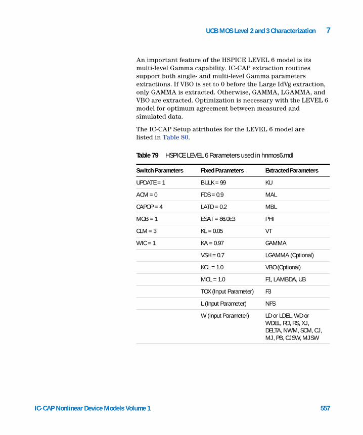
UCB MOS Level 2 and 3 Characterization 7
IC-CAP Nonlinear Device Models Vo
An important feature of the HSPICE LEVEL 6 model is its multi-level Gamma capability. IC-CAP extraction routines support both single- and multi-level Gamma parameters extractions. If VBO is set to 0 before the Large IdVg extraction, only GAMMA is extracted. Otherwise, GAMMA, LGAMMA, and VBO are extracted. Optimization is necessary with the LEVEL 6 model for optimum agreement between measured and simulated data.
The IC-CAP Setup attributes for the LEVEL 6 model are listed in Table 80.
Table 79 HSPICE LEVEL 6 Parameters used in hnmos6.mdl
Switch Parameters Fixed Parameters Extracted Parameters
UPDATE = 1 BULK = 99 KU
ACM = 0 FDS = 0.9 MAL
CAPOP = 4 LATD = 0.2 MBL
MOB = 1 ESAT = 86.0E3 PHI
CLM = 3 KL = 0.05 VT
WIC = 1 KA = 0.97 GAMMA
VSH = 0.7 LGAMMA (Optional)
KCL = 1.0 VBO (Optional)
MCL = 1.0 F1, LAMBDA, UB
TOX (Input Parameter) F3
L (Input Parameter) NFS
W (Input Parameter) LD or LDEL, WD or WDEL, RD, RS, XJ, DELTA, NWM, SCM, CJ, MJ, PB, CJSW, MJSW
lume 1 557

7 UCB MOS Level 2 and 3 Characterization
Measurement
Table 80 HSPICE LEVEL 6 Model Setup Attributes
DUT/Setup
Inputs Outputs Tranform Function Extractions
large/idvg
vg, vb, vd, vs id extract MOSDC_lev6_lin_large PHI, VT, GAMMA, LGAMMA, VBO, LAMBDA, UB, NFS
optimize Optimize PHI, VT, GAMMA, LGAMMA, VBO F1, F3
opt_NFS Optimize NFS
narrow/idvg
// // extract MOSDC_lev6_lin_narrow NWM, WD(EL), DELTA
optimize Optimize NWM, WDEL
short/idvg
// // extract MOSDC_lev6_lin_short SCM, XJ, LD(EL)
optimize Optimize SCM, XJ, LDEL, RD, RS
short/idvd
vd, vg, vb, vs id optimize Optimize KU, MAL, LAMBDA, MBL
cbd1/cjdarea
vb, vd cbd set_CJ Program initial zero bias CJ
extract Optimize CJ, MJ, PB
cbd2/cjdperimeter
vb, vd cbd extract MOSCV_total_cap CJ, MJ, CJSW, MJSW, PB
558
The measurement setups are identical to the UCB MOS LEVEL 2 and LEVEL 3 model example files. However, to obtain accurate GAMMA and LGAMMA parameters for ion-implanted devices, the measured data must clearly express the body effects. Therefore, the bulk voltage should be set broadly on the Large IdVg measurement. The following sequence for DC measurements is recommended:
1 Large IdVg
2 Narrow IdVg
3 Short IdVg
4 Short IdVd
IC-CAP Nonlinear Device Models Volume 1
UCB MOS Level 2 and 3 Characterization 7
Extraction and Optimization
IC-CAP Nonlinear Device Models Vo
All DC parameters are extracted and optimized with the DCExtraction macro. Alternately, extractions and optimizations can be performed interactively as described for the LEVEL 2 and LEVEL 3 MOSFET models. There is no extraction routine in the short IdVd setup for saturation region parameters. Instead, the parameters KU, MAL, MBL, and LAMBDA must be optimized. For certain devices it may be necessary to alter the optimization setup and default parameter values for accurate results.
lume 1 559
7 UCB MOS Level 2 and 3 Characterization
References
560
1 A. Vladmirescu and Sally Liu. Simulation of MOS Integrated Circuits Using SPICE2, UCB/ERL M80/7, University of California at Berkeley.
2 HSPICE User’s Manual, H92 Release, Meta-Software, Inc., 1992.
IC-CAP Nonlinear Device Models Volume 1
Agilent 85190A IC-CAP 2008Nonlinear Device Models Volume 1
8Bipolar Transistor Characterization
Bipolar Device Model 563
Simulators 564
Model Parameters 565
Test Instruments 571
Measuring and Extracting 573
Extraction Algorithms 582
References 586
This chapter describes the University of California at Berkeley bipolar transistor model supported in SPICE. Descriptions of model setup, instrument connections, and model parameters are included. Information is included for making DC, capacitance, and high-frequency AC measurements and their corresponding extractions.
The IC-CAP bipolar modeling module provides setups that can be used for general measurement and model extraction for bipolar devices. Two example files are provided for the bipolar model; the example files can also be used as a template for creating custom model configurations.
bjt_npn.mdl extracts parameters for NPN bipolar transistors
bjt_pnp.mdl extracts parameters for PNP bipolar transistors
The IC-CAP system offers the flexibility to modify any measurement or simulation specification.
561Agilent Technologies
562
8 Bipolar Transistor Characterization
The model extractions provided are also intended for general bipolar IC processes. If you have another method of extracting specific model parameters, you can do so with the Program function by writing a function in C and linking it to the function list. For Program function details or for writing user-defined C-language routines, refer to Chapter 9, “Using Transforms and Functions,” in the IC-CAP User’s Guide.
The following shows an example custom extraction for IS and NF:! Extraction for IS & NF! Note: print statements go to the! window that started IC-CAPprint "Example Custom Extraction for IS & NF"index = 0 ! array index! pick two low current pointsv1 = -ve[index]WHILE v1 < 0.4 ! get a point near Vbe = 0.4 index = index + 1 v1 = -ve[index]END WHILEi1 = ic.m[index]v2 = -ve[index]WHILE v2 < 0.5 ! get a point near Vbe = 0.5 index = index + 1 v2 = -ve[index]END WHILEi2 = ic.m[index]! extract IS & NFvt = 8.62e-5 * (TNOM + 273.15) ! thermal voltageNF = 1 / vt * (v2 - v1) / log(i2 / i1)IS = sqrt(i1 * i2) / exp((v1 + v2) / (2 * NF * vt))print "IS = ";IS;" NF = ";NFprint "... end of custom extraction ..."
IC-CAP Nonlinear Device Models Volume 1
Bipolar Transistor Characterization 8
Bipolar Device Model
IC-CAP Nonlinear Device Models Vo
The UCB bipolar transistor model is a hybrid of the Ebers-Moll [2] and Gummel-Poon [3] models. With a minimum parameter specification of IS, BF, and BR, the model defaults to the more simple Ebers-Moll model. The Ebers-Moll model is ideal because it neglects base width modulation, parasitic resistances, and high current injection effects.
Inclusion of additional parameters activates elements of the Gummel-Poon integral charge control model, which can provide greater accuracy. The Gummel-Poon model provides superior representation of the current flow in the transistor’s base. It also provides accurate representation of parasitic resistances at all terminals, capacitance across all junctions, current-frequency effects, and temperature effects.
lume 1 563

8 Bipolar Transistor Characterization
Simulators
564
The UCB bipolar model is supported by all SPICE simulators currently included with IC-CAP: HPSPICE, SPICE2(G6), and SPICE3.
NOTE Simulators are provided as a courtesy to IC-CAP users; they are not supported by Agilent Technologies.
The default nominal temperature for HPSPICE is 25°C. For SPICE2 and SPICE3 it is 27°C. To force a nominal temperature, set the TNOM variable to the desired value.
IC-CAP Nonlinear Device Models Volume 1
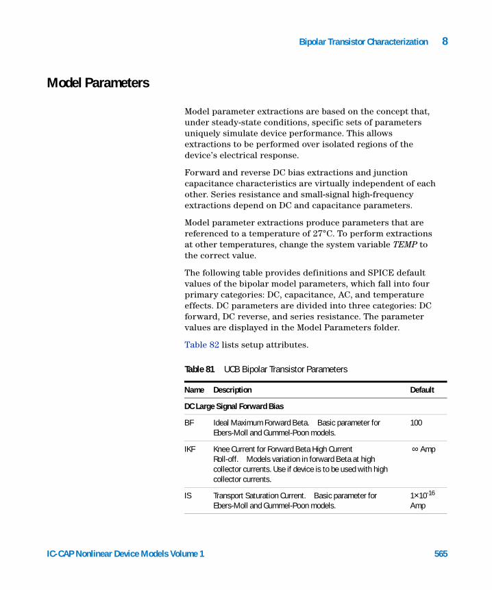
Bipolar Transistor Characterization 8
Model Parameters
IC-CAP Nonlinear Device Models Vo
Model parameter extractions are based on the concept that, under steady-state conditions, specific sets of parameters uniquely simulate device performance. This allows extractions to be performed over isolated regions of the device’s electrical response.
Forward and reverse DC bias extractions and junction capacitance characteristics are virtually independent of each other. Series resistance and small-signal high-frequency extractions depend on DC and capacitance parameters.
Model parameter extractions produce parameters that are referenced to a temperature of 27°C. To perform extractions at other temperatures, change the system variable TEMP to the correct value.
The following table provides definitions and SPICE default values of the bipolar model parameters, which fall into four primary categories: DC, capacitance, AC, and temperature effects. DC parameters are divided into three categories: DC forward, DC reverse, and series resistance. The parameter values are displayed in the Model Parameters folder.
Table 82 lists setup attributes.
Table 81 UCB Bipolar Transistor Parameters
Name Description Default
DC Large Signal Forward Bias
BF Ideal Maximum Forward Beta. Basic parameter for Ebers-Moll and Gummel-Poon models.
100
IKF Knee Current for Forward Beta High Current Roll-off. Models variation in forward Beta at high collector currents. Use if device is to be used with high collector currents.
∞ Amp
IS Transport Saturation Current. Basic parameter for Ebers-Moll and Gummel-Poon models.
1×10-16 Amp
lume 1 565
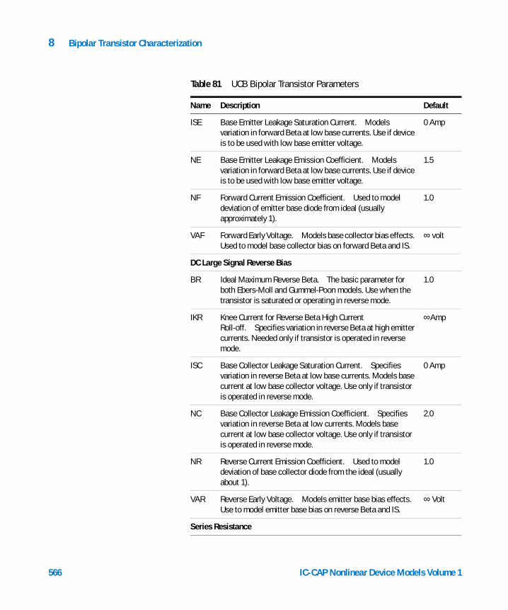
566
8 Bipolar Transistor Characterization
ISE Base Emitter Leakage Saturation Current. Models variation in forward Beta at low base currents. Use if device is to be used with low base emitter voltage.
0 Amp
NE Base Emitter Leakage Emission Coefficient. Models variation in forward Beta at low base currents. Use if device is to be used with low base emitter voltage.
1.5
NF Forward Current Emission Coefficient. Used to model deviation of emitter base diode from ideal (usually approximately 1).
1.0
VAF Forward Early Voltage. Models base collector bias effects. Used to model base collector bias on forward Beta and IS.
∞ volt
DC Large Signal Reverse Bias
BR Ideal Maximum Reverse Beta. The basic parameter for both Ebers-Moll and Gummel-Poon models. Use when the transistor is saturated or operating in reverse mode.
1.0
IKR Knee Current for Reverse Beta High Current Roll-off. Specifies variation in reverse Beta at high emitter currents. Needed only if transistor is operated in reverse mode.
∞Amp
ISC Base Collector Leakage Saturation Current. Specifies variation in reverse Beta at low base currents. Models base current at low base collector voltage. Use only if transistor is operated in reverse mode.
0 Amp
NC Base Collector Leakage Emission Coefficient. Specifies variation in reverse Beta at low currents. Models base current at low base collector voltage. Use only if transistor is operated in reverse mode.
2.0
NR Reverse Current Emission Coefficient. Used to model deviation of base collector diode from the ideal (usually about 1).
1.0
VAR Reverse Early Voltage. Models emitter base bias effects. Use to model emitter base bias on reverse Beta and IS.
∞ Volt
Series Resistance
Table 81 UCB Bipolar Transistor Parameters
Name Description Default
IC-CAP Nonlinear Device Models Volume 1
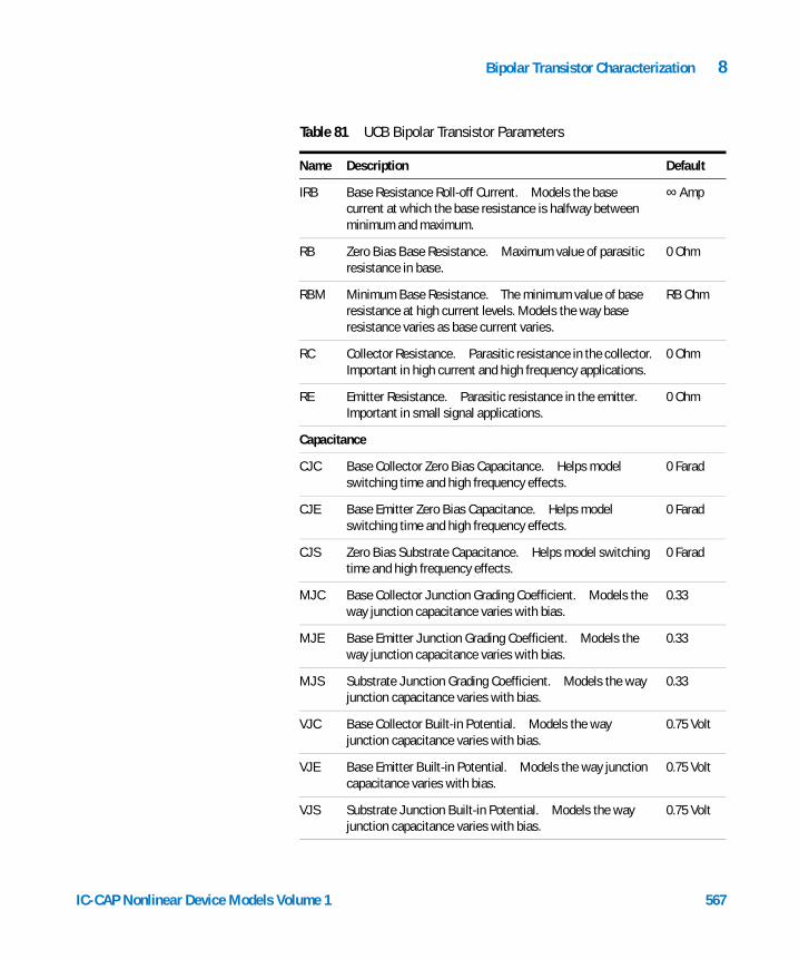
Bipolar Transistor Characterization 8
IC-CAP Nonlinear Device Models Vo
IRB Base Resistance Roll-off Current. Models the base current at which the base resistance is halfway between minimum and maximum.
∞ Amp
RB Zero Bias Base Resistance. Maximum value of parasitic resistance in base.
0 Ohm
RBM Minimum Base Resistance. The minimum value of base resistance at high current levels. Models the way base resistance varies as base current varies.
RB Ohm
RC Collector Resistance. Parasitic resistance in the collector. Important in high current and high frequency applications.
0 Ohm
RE Emitter Resistance. Parasitic resistance in the emitter. Important in small signal applications.
0 Ohm
Capacitance
CJC Base Collector Zero Bias Capacitance. Helps model switching time and high frequency effects.
0 Farad
CJE Base Emitter Zero Bias Capacitance. Helps model switching time and high frequency effects.
0 Farad
CJS Zero Bias Substrate Capacitance. Helps model switching time and high frequency effects.
0 Farad
MJC Base Collector Junction Grading Coefficient. Models the way junction capacitance varies with bias.
0.33
MJE Base Emitter Junction Grading Coefficient. Models the way junction capacitance varies with bias.
0.33
MJS Substrate Junction Grading Coefficient. Models the way junction capacitance varies with bias.
0.33
VJC Base Collector Built-in Potential. Models the way junction capacitance varies with bias.
0.75 Volt
VJE Base Emitter Built-in Potential. Models the way junction capacitance varies with bias.
0.75 Volt
VJS Substrate Junction Built-in Potential. Models the way junction capacitance varies with bias.
0.75 Volt
Table 81 UCB Bipolar Transistor Parameters
Name Description Default
lume 1 567
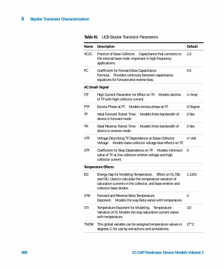
568
8 Bipolar Transistor Characterization
XCJC Fraction of Base Collector. Capacitance that connects to the internal base node. Important in high frequency applications.
1.0
FC Coefficient for Forward Bias Capacitance Formula. Provides continuity between capacitance equations for forward and reverse bias.
0.5
AC Small-Signal
ITF High Current Parameter for Effect on TF. Models decline of TF with high collector current.
∞ Amp
PTF Excess Phase at FT. Models excess phase at FT. 0 Degree
TF Ideal Forward Transit Time. Models finite bandwidth of device in forward mode.
0 Sec
TR Ideal Reverse Transit Time. Models finite bandwidth of device in reverse mode.
0 Sec
VTF Voltage Describing TF Dependence on Base-Collector Voltage. Models base-collector voltage bias effects on TF.
∞ Volt
XTF Coefficient for Bias Dependence on TF. Models minimum value of TF at low collector-emitter voltage and high collector current.
0
Temperature Effects
EG Energy Gap for Modeling Temperature. Effect on IS, ISE, and ISC. Used to calculate the temperature variation of saturation currents in the collector, and base-emitter and collector base diodes.
1.11EV
XTB Forward and Reverse Beta Temperature Exponent. Models the way Beta varies with temperature.
0
XTI Temperature Exponent for Modeling. Temperature Variation of IS. Models the way saturation current varies with temperature.
3.0
TNOM This global variable can be assigned temperature values in degrees C, for use by extractions and simulations.
27°C
Table 81 UCB Bipolar Transistor Parameters
Name Description Default
IC-CAP Nonlinear Device Models Volume 1
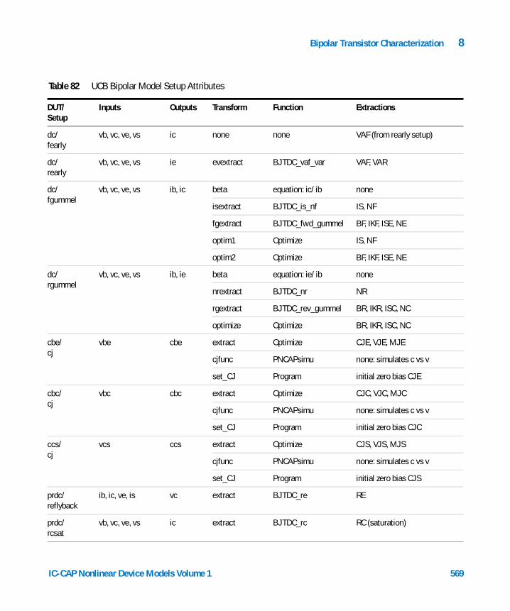
Bipolar Transistor Characterization 8
Table 82 UCB Bipolar Model Setup Attributes
DUT/Setup
Inputs Outputs Transform Function Extractions
dc/fearly
vb, vc, ve, vs ic none none VAF (from rearly setup)
dc/rearly
vb, vc, ve, vs ie evextract BJTDC_vaf_var VAF, VAR
dc/fgummel
vb, vc, ve, vs ib, ic beta equation: ic/ib none
isextract BJTDC_is_nf IS, NF
fgextract BJTDC_fwd_gummel BF, IKF, ISE, NE
optim1 Optimize IS, NF
optim2 Optimize BF, IKF, ISE, NE
dc/rgummel
vb, vc, ve, vs ib, ie beta equation: ie/ib none
nrextract BJTDC_nr NR
rgextract BJTDC_rev_gummel BR, IKR, ISC, NC
optimize Optimize BR, IKR, ISC, NC
cbe/cj
vbe cbe extract Optimize CJE, VJE, MJE
cjfunc PNCAPsimu none: simulates c vs v
set_CJ Program initial zero bias CJE
cbc/cj
vbc cbc extract Optimize CJC, VJC, MJC
cjfunc PNCAPsimu none: simulates c vs v
set_CJ Program initial zero bias CJC
ccs/cj
vcs ccs extract Optimize CJS, VJS, MJS
cjfunc PNCAPsimu none: simulates c vs v
set_CJ Program initial zero bias CJS
prdc/reflyback
ib, ic, ve, is vc extract BJTDC_re RE
prdc/rcsat
vb, vc, ve, vs ic extract BJTDC_rc RC (saturation)
IC-CAP Nonlinear Device Models Volume 1 569
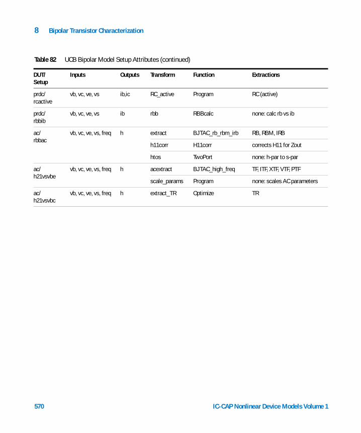
8 Bipolar Transistor Characterization
prdc/rcactive
vb, vc, ve, vs ib,ic RC_active Program RC (active)
prdc/rbbib
vb, vc, ve, vs ib rbb RBBcalc none: calc rb vs ib
ac/rbbac
vb, vc, ve, vs, freq h extract BJTAC_rb_rbm_irb RB, RBM, IRB
h11corr H11corr corrects H11 for Zout
htos TwoPort none: h-par to s-par
ac/h21vsvbe
vb, vc, ve, vs, freq h acextract BJTAC_high_freq TF, ITF, XTF, VTF, PTF
scale_params Program none: scales AC parameters
ac/h21vsvbc
vb, vc, ve, vs, freq h extract_TR Optimize TR
Table 82 UCB Bipolar Model Setup Attributes (continued)
DUT/Setup
Inputs Outputs Transform Function Extractions
570 IC-CAP Nonlinear Device Models Volume 1
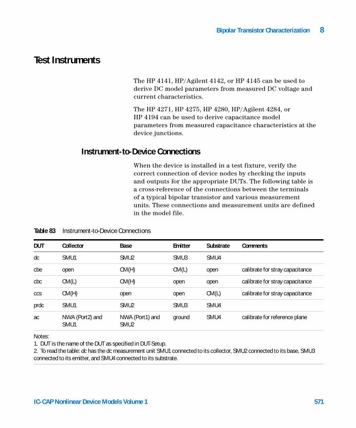
Bipolar Transistor Characterization 8
Test Instruments
IC-CAP Nonlinear Device Models Vo
The HP 4141, HP/Agilent 4142, or HP 4145 can be used to derive DC model parameters from measured DC voltage and current characteristics.
The HP 4271, HP 4275, HP 4280, HP/Agilent 4284, or HP 4194 can be used to derive capacitance model parameters from measured capacitance characteristics at the device junctions.
Instrument-to-Device Connections
When the device is installed in a test fixture, verify the correct connection of device nodes by checking the inputs and outputs for the appropriate DUTs. The following table is a cross-reference of the connections between the terminals of a typical bipolar transistor and various measurement units. These connections and measurement units are defined in the model file.
nections
Table 83 Instrument-to-Device ConDUT Collector Base Emitter Substrate Comments
dc SMU1 SMU2 SMU3 SMU4
cbe open CM(H) CM(L) open calibrate for stray capacitance
cbc CM(L) CM(H) open open calibrate for stray capacitance
ccs CM(H) open open CM(L) calibrate for stray capacitance
prdc SMU1 SMU2 SMU3 SMU4
ac NWA (Port2) and SMU1
NWA (Port1) and SMU2
ground SMU4 calibrate for reference plane
Notes:1. DUT is the name of the DUT as specified in DUT-Setup.2. To read the table: dc has the dc measurement unit SMU1 connected to its collector, SMU2 connected to its base, SMU3 connected to its emitter, and SMU4 connected to its substrate.
lume 1 571
572
8 Bipolar Transistor Characterization
Input and output tables in the various setups use abbreviations C (collector), B (base), E (emitter), and S (substrate) for the bipolar transistor nodes. These nodes are defined in the Circuit folder.
Measurement units (abbreviated as follows) are defined in Hardware Setup.
SMU# for DC measurement units
VM# for voltage monitor units
VS# for voltage source units
CM for capacitance measurement units
NWA for network analyzer port units
IC-CAP Nonlinear Device Models Volume 1
Bipolar Transistor Characterization 8
Measuring and Extracting
IC-CAP Nonlinear Device Models Vo
Bipolar parameter extraction is divided into four categories: DC, capacitance, parasitic resistance, and AC. These categories correspond to the required supporting measurements described under Test Instruments.
The bjt_npn.mdl file provides DUTs and setups that correctly bias a typical device for the measurements needed to perform the associated parameter extractions.
Measurement and Extraction Guidelines
The following guidelines are provided to help you achieve more successful model measurements and extractions.
Setting Instrument Options
Before starting a measurement, you can quickly verify the instrument options settings. Save the current instrument option settings by saving the model file to <file_name>.mdl. Some of the Instrument Options specify instrument calibration. For the most accurate results, calibrate the instruments before taking IC-CAP measurements.
Typical DC and cv instrument options are:
• DC measurements are generally taken with Integration Time = Medium.
• CV measurements in the femtofarad region usually require High Resolution = Yes and Measurement Freq (kHz) = 1000.
When taking AC measurements with a network analyzer, several instrument settings are critical. And, calibration must be performed on structures that have impedances similar to the stray parasitics of the device under test (DUT).
Typical AC instrument options are:
• Input power to the device is typically −10 to −30dBm (after port attenuation).
lume 1 573
574
8 Bipolar Transistor Characterization
• Setting the averaging factor in the 2 to 4 range reduces measurement noise.
• Because IC-CAP requires the instrument to perform error correction, set Use Internal Calibration = Yes.
NOTE The error terms saved to file during a network analyzer software calibration are not identified by error code.
The order shown below represents the order in which they are saved and displayed in IC-CAP:
0. EDF [directivity] 1. EDR [directivity] 2. EXF [isolation] 3. EXR [isolation] 4. ESF [source match] 5. ERF [ref freq response] 6. ESR [source match] 7. ERR [ref freq response] 8. ELF [load match] 9. ETF [trans freq response] 10. ELR [load match] 11. ETR [trans freq response]
Experiment with the other network analyzer options to obtain the best results with specific devices.
Measuring Instruments
Ensure that the measuring instruments (specified by unit names in the inputs and outputs) are correctly connected to the DUT. Refer to Table 83 for a list of nodes and corresponding measurement units. The quality of the measuring equipment (instruments, cables, test fixture, transistor sockets, and probes) can influence the noise level in the measurements.
The series resistance in test fixtures can also be critical when making high current measurements. For example, a 1-ohm resistance in series with the emitter at an Ic = 20 mA can cause a factor-of-two error in the measured
IC-CAP Nonlinear Device Models Volume 1
Bipolar Transistor Characterization 8
IC-CAP Nonlinear Device Models Vo
versus simulated DC performance. Series resistances that are not accounted for in the device model can be included by adding them to the test circuit for the DUT.
Ensure that all characteristics of the measurement stimulus and corresponding measured response are specified in the respective input and output tables.
For some measurements, the instruments or test hardware must be calibrated to remove non-device parasitics from the DUT. For bipolar devices, stray capacitance due to probe systems, bond pads, and so on should be calibrated out prior to each measurement.
In making high-frequency two-port measurements with a network analyzer, the reference plane of the instrument must be calibrated out to the DUT. IC-CAP relies on the internal calibration of the instruments for full error-corrected data. Calibration using OPEN, SHORT, THRU, and 50-ohm LOADS must be correctly performed.
Extracting Model Parameters
For a given setup, you can find the extraction transforms in the Extract/Optimize folder. IC-CAP’s extraction algorithms exist as functions; choose Browse to list the functions available for a setup.
When the Extract command is selected from the setup, all extractions in the setup are performed in the order listed in the setup. This order is usually critical to proper extraction performance. Extractions are typically completed instantly and the newly extracted model parameter values are placed in Model Parameters.
Simulating Device Response
Simulation uses model parameter values currently in Model Parameters. A SPICE deck is created and the simulation performed. The output of the SPICE simulation is then read into IC-CAP as simulated data.
lume 1 575
576
8 Bipolar Transistor Characterization
Select a simulator from Tools > Hardware Setup or define a SIMULATOR variable. Simulations vary in the amount of time they take to complete. DC simulations generally run much faster than cv and AC simulations.
If simulated results are not as expected, use the Simulation Debugger (Tools menu) to examine the input and output simulation files. The output of manual simulations is not available for further processing by IC-CAP functions (such as transforms and plots). For more information refer to “Using the Simulation Debugger" in the IC-CAP User’s Guide.
Displaying Plots
The Display Plot function displays all graphical plots defined in a setup. The currently active graphs are listed in the Plots folder in each setup.
Measured data is displayed as a solid line; simulated data is displayed as a dashed or dotted line of the same color. After an extraction and subsequent simulation, view the plots for agreement between measured and simulated data. Plots are automatically updated each time a measurement or simulation is performed.
Optimizing Model Parameters
Optimization of model parameters improves the agreement between measured and simulated data. The bipolar model typically requires very little optimization because most of the extraction algorithms have some optimization built into them.
Capacitance parameter extractions are actually done through optimization. An Optimize Transform whose Extract Flag is set to Yes is automatically called after any extraction that precedes it in the Transform list.
Optimizing AC parameters can be very time-consuming because of the number of SPICE simulations required.
IC-CAP Nonlinear Device Models Volume 1
Bipolar Transistor Characterization 8
IC-CAP Nonlinear Device Models Vo
PNP Transistors
In the bjt_pnp.mdl file included with IC-CAP, PNP transistors are measured, extracted, and simulated in a manner similar to NPN transistors. The critical difference with a PNP device is that the bias voltages are of opposite polarity from an NPN device.
To extract the two models using the same algorithms, set a variable in Model Variables; POLARITY should have the value PNP. The extraction default NPN will result in incorrect parameter values or extraction errors on PNP data.
Another variable convenient for displaying PNP Plots is inv_plot. This variable can invert the plots in bjt_pnp.mdl so they plot in the same direction as NPN plots. Set inv_plot to -1 to do this.
Extracting Parameters
This section describes the general process for extracting model parameter data from the UCB bipolar transistor. The process applies to all types of parameters: DC, capacitance, and AC. The differences between extracting one type of parameter and another are primarily in the types of instruments used to measure the data and the specifications within the DUTs and setups.
Parameters are typically extracted from measured data but can also be extracted from simulated data. To extract from measured data, ensure that the outputs specified in the extraction transforms use the .m suffix. For example, IS and NF are extracted using the BJTDC_is_nf function. To extract from measured data, IC-CAP uses log10(ic.m) as the specification of the forward collector current. (Use the .s suffix when extracting from simulated data.)
When performing an extraction, accurate results depend on the sequence of steps. The top-to-bottom order of DUTs and setups in a model file is the suggested order of measurements and extractions. In the bjt_npn.mdl file, the large signal DC and junction capacitance parameters are independent of each other. However, for the parasitic
lume 1 577
578
8 Bipolar Transistor Characterization
resistances and AC parameters to be accurately extracted, the preceding two groups must be successfully extracted first. Setups in bjt_npn.mdl are designed for use with a typical bipolar transistor. You may be able to improve results with your own devices by modifying these setups to more closely conform to your needs.
The general extraction procedure is summarized next, starting with the measurement process.
1 Install the device to test in a test fixture and connect the measuring instruments.
2 Ensure the test fixture, signal sources and measuring instruments, and workstation are physically and logically configured to the IC-CAP system.
3 Load the model.
4 Select the DUT and setup.
NOTE Execute measurements and extractions in the order listed in DUTs-Setups to ensure the correct order; otherwise, incorrect results may result.
5 Issue the Measure command.
6 Issue the Extract command.
7 Issue the Simulate command.
8 Display the results.
9 Fine tune the extracted parameters if needed by optimizing.
DC Large-Signal Parameters
Setups are provided for measuring and extracting the properties of the internal transistor (not including parasitic resistances); these are fearly, rearly, fgummel, and rgummel.
IC-CAP Nonlinear Device Models Volume 1
Bipolar Transistor Characterization 8
IC-CAP Nonlinear Device Models Vo
The fearly and rearly setups measure forward and reverse Early voltage characteristics, respectively. The Early voltage parameters VAF and VAR are extracted simultaneously in the rearly setup, using measurements taken from both fearly and rearly.
The fgummel and rgummel setups perform the forward and reverse Gummel plot measurements. Parameters IS, BF, NE, IKF, ISE, and NF are extracted by the fgummel setup, while the extractions in the rgummel setup produce the BR, NR, IKR, ISC, and NC parameters. The model uses the saturated current parameter IS to simulate current flow in both directions.
Junction Capacitance Parameters
Measuring bipolar transistor capacitance characteristics requires three DUTs. This is because each p-n junction is a physically different one-port connection. The base-emitter, base-collector, and collector-substrate junctions each have a different DUT and setup. While you will perform all three measurements on the same physical device, each measurement requires different instrument connections for the corresponding DUT and setup. The DUTs and instrument connections for each measurement are listed in Table 83.
Each p-n junction is measured from a small forward bias to a large reverse bias. The extractions are performed using the transform set_CJ to find the initial value of CJ0, then optimizing the parameters of the general p-n junction capacitance equation to the measured data. This produces the capacitance, built-in voltage, and grading factors for each DUT: CJE, VJE, MJE; CJC, VJC, MJC; CJS, VJS, MJS. For the most accurate extractions, calibrate out stray capacitance from cables, probes, and bond pads before taking each p-n junction capacitance measurement.
DC Parasitic Resistance Parameters
Three parasitic resistances are connected to the bipolar transistor: RE, RC, and RB. RE and RC are constant value components, while RB is a function of base current. RE is
lume 1 579

580
8 Bipolar Transistor Characterization
measured by the setup reflyback. This setup saturates the transistor, then measures the differential voltage drop from collector to emitter (with Ic = 0) versus the differential base-to-emitter current.
RC is measured by the setup rcsat, which measures the parameter as the DC resistance from collector to emitter at the onset of saturation. Alternately, the rcactive setup can be used to measure the collector resistance in the active region of device operation. However, this extraction is dependent on the operating point, which must be specified by manually placing a box on the Plot contained in the setup. For complete information on using this extraction, refer to HP Application Note Advanced Bipolar Transistor Modeling Techniques[1].
The setup rbbib does not actually measure or extract RB. Instead, it produces a characteristic curve of base-to-emitter bias versus DC base current. The resulting curve is used when the base resistance is measured and extracted using S-parameters.
Base Resistance and Transit Time Parameters
The AC DUT uses setups that measure S-parameters with a network analyzer. The quality of the measured S-parameters depends on the calibration of the network analyzer. IC-CAP does not perform error correction; it relies totally on the measuring instruments for the correction of errors.
Making high-frequency measurements on packaged transistors can lead to unexpected results. This is because of the stray capacitance and inductance that are a part of the package. Measure S-parameters with a high-quality microwave wafer probe.
The AC setup rbbac measures H11 of the transistor in the common emitter mode. This input impedance is then used in the extraction to produce model parameters RB, IRB, and RBM.
IC-CAP Nonlinear Device Models Volume 1
Bipolar Transistor Characterization 8
IC-CAP Nonlinear Device Models Vo
The AC setup h21vsvbe measures H21 of the transistor in the common emitter mode. The measured current gain is then used to extract a small signal model that produces the parameters TF, ITF, VTF, XTF, and PTF.
The AC setup h21vsvbc measures H21 of the transistor in the common collector mode. The measured current gain is then used to extract the parameter TR.
lume 1 581
8 Bipolar Transistor Characterization
Extraction Algorithms
582
This section describes the extraction algorithms used for DC, capacitance, parasitic resistance, and AC model parameters of the bipolar transistor.
DC Parameter Extractions
The Early voltage extractions produce the model parameters VAF and VAR. The output conductance of Ic versus Vce for steps of Vb is used in the calculation. Both Early parameters are extracted simultaneously, which requires both forward and reverse measurements prior to extraction. The actual extraction is performed under the rearly setup. The substrate bias should be held at a negative (positive) voltage for an NPN (PNP) transistor. For the extraction to function correctly, the device must be completely out of saturation at the 20 percent point of each curve, and the forward and reverse curves must have the same number of steps.
The forward Gummel measurement is used to extract IS, NF, BF, IKF, ISE, and NE. This measurement holds the base-collector voltage at approximately 0V and drives the emitter with a negative bias sweep. The bias should produce Ic in the range of less than 1nA to more than 10 mA for a typical IC transistor.
First, IS and NF are extracted from the low current region of the Ic versus Vbe data using a least-squares fit. The very low current region of the Ib versus Vbe data is used to obtain ISE and NE, the base recombination parameters. An internal optimization in the extraction algorithm is then used to produce BF and IKF and fine-tune the ISE and NE parameters. If insufficient high current data is available, IKF will be set to a default value of 10A. To guarantee that IKF is extracted, measure until beta has rolled off to approximately half of its peak value.
The reverse Gummel measurement is used to extract NR, BR, IKR, ISC, and NC. This measurement and extraction is analogous to the forward measurement except that the
IC-CAP Nonlinear Device Models Volume 1
Bipolar Transistor Characterization 8
IC-CAP Nonlinear Device Models Vo
transistor is now in the reverse active mode. If the measurement is made on an IC structure that has a substrate of opposite polarity to the collector, it is possible that the plot of reverse Beta versus Ie will not fit well. This is because the parasitic transistor formed by the base-to-collector-to-substrate begins to conduct, thus robbing current from the base of the transistor being modeled. There is a solution to this problem. The example file npnwpnp.mdl includes a compound structure of both an NPN transistor and its parasitic PNP device. This model allows you to produce an excellent fit of the NPN transistor operating in the reverse bias region. Refer to “Circuit Parameter Extraction” on page 715 for more information on using this file to characterize the reverse active mode of operation.
Capacitance Parameter Extractions
The capacitances are split into three different DUTs. The measurement is performed over a range of small forward bias (where v < VJ ⋅ FC) to at least several volts of reverse bias. The parameter extraction is accomplished through optimization of the controlling parameters in the characteristic equation for the junction capacitance. The extraction from each produces the zero bias capacitance CJx, the built-in potential of the junction VJx, and the grading factor of the junction MJx. The forward bias coefficient FC is set to the SPICE default value of 0.5. The purpose of this parameter is to switch the capacitance in the simulator into a linear model before the junction bias approaches VJx.
Parasitic DC Parameter Extractions
This set of setups uses DC measurements to obtain the emitter resistance RE, the collector resistance RC, and a DC I versus V relationship to be used later in the base resistance extraction. RE is extracted from a measurement of the differential of collector voltage with respect to base current with the transistor biased into saturation. A linear fit is performed on the part of the curve that is most sensitive to the effects of RE.
lume 1 583
584
8 Bipolar Transistor Characterization
In the rcsat setup RC is extracted from a measurement of Ic versus Vce with the base biased so that the transistor is near its peak Beta point and well into saturation. The extraction uses a linear fit along with the known RE. In the rcactive setup RC is extracted at a bias selected by placing a box on the Plot of Ic versus Vce.
The setup rbbib is not actually used to extract any model parameters directly but is used by the following AC measurements in the extraction of the base resistance parameters. The base voltage bias specification used in this setup and in the rbbac setup must be the same. To facilitate this, the start value, stop value, and number of points are set using four variables in the model level variable table. These are rbbstart, rbbstop, rbbnpts, and rbbvc. The start and stop bias voltages should sweep the transistor’s operating point from near peak Beta to well into Beta roll-off.
AC Parameter Extractions
Base resistance and transit time parameters are extracted from network analyzer measurements of the transistor’s S-parameters converted to H-parameters. Both of these sets of model parameters are highly dependent upon the prior extraction of the DC, capacitance, and parasitic resistance parameters.
The base resistance is extracted from H11 data versus frequency and bias. The H11 data traces a circular path on a Re-Im axis system versus frequency. The measurement frequency should be held low enough so that this circular pattern does not start to become linear. This characteristic is used to obtain the real value of Rbase versus base current. From the characteristic of Rbase versus Ibase, the RB, IRB, and RBM parameters are extracted.
The transit time parameters, TF, XTF, ITF, VTF, and PTF, are extracted from measurements of the common-emitter current gain H21. The measurement frequency should be higher than the -3dB roll-off frequency of the transistor at all bias levels. However, the measurement frequency should also be
IC-CAP Nonlinear Device Models Volume 1
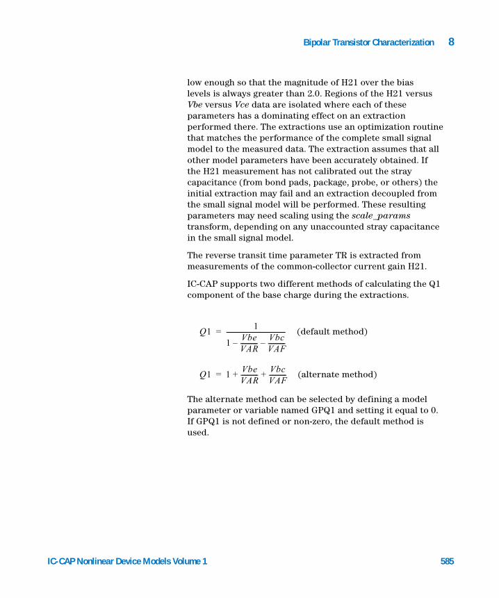
Bipolar Transistor Characterization 8
IC-CAP Nonlinear Device Models Vo
low enough so that the magnitude of H21 over the bias levels is always greater than 2.0. Regions of the H21 versus Vbe versus Vce data are isolated where each of these parameters has a dominating effect on an extraction performed there. The extractions use an optimization routine that matches the performance of the complete small signal model to the measured data. The extraction assumes that all other model parameters have been accurately obtained. If the H21 measurement has not calibrated out the stray capacitance (from bond pads, package, probe, or others) the initial extraction may fail and an extraction decoupled from the small signal model will be performed. These resulting parameters may need scaling using the scale_params transform, depending on any unaccounted stray capacitance in the small signal model.
The reverse transit time parameter TR is extracted from measurements of the common-collector current gain H21.
IC-CAP supports two different methods of calculating the Q1 component of the base charge during the extractions.
(default method)
(alternate method)
The alternate method can be selected by defining a model parameter or variable named GPQ1 and setting it equal to 0. If GPQ1 is not defined or non-zero, the default method is used.
Q11
1VbeVAR-----------
VbcVAF-----------––
--------------------------------------=
Q1 1VbeVAR-----------
VbcVAF-----------+ +=
lume 1 585
8 Bipolar Transistor Characterization
References
586
1 Advanced Bipolar Transistor Modeling Techniques, HP Application Note 1201-4, Publication #5091-2503EUS, July, 1991.
2 J.J. Ebers and J.L. Moll, Large-Signal Behaviour of Junction Transistors, Proc. IRE, No. 42, 1954.
3 H.K. Gummel and H.C. Poon, An Integral Charge Control Model of Bipolar Transistors, Bell Systems Technical Journal, No. 49, 1970.
IC-CAP Nonlinear Device Models Volume 1

Agilent 85190A IC-CAP 2008Nonlinear Device Models Volume 1
9Agilent-HBT Modeling Package
This chapter describes the Agilent-HBT Modeling Package (Toolkit) including measurement and extraction of Agilent-HBT Model parameters. This chapter also shows you how to use the toolkit with descriptions of general settings, and how measurement/extraction works for HBT device modeling.
587Agilent Technologies
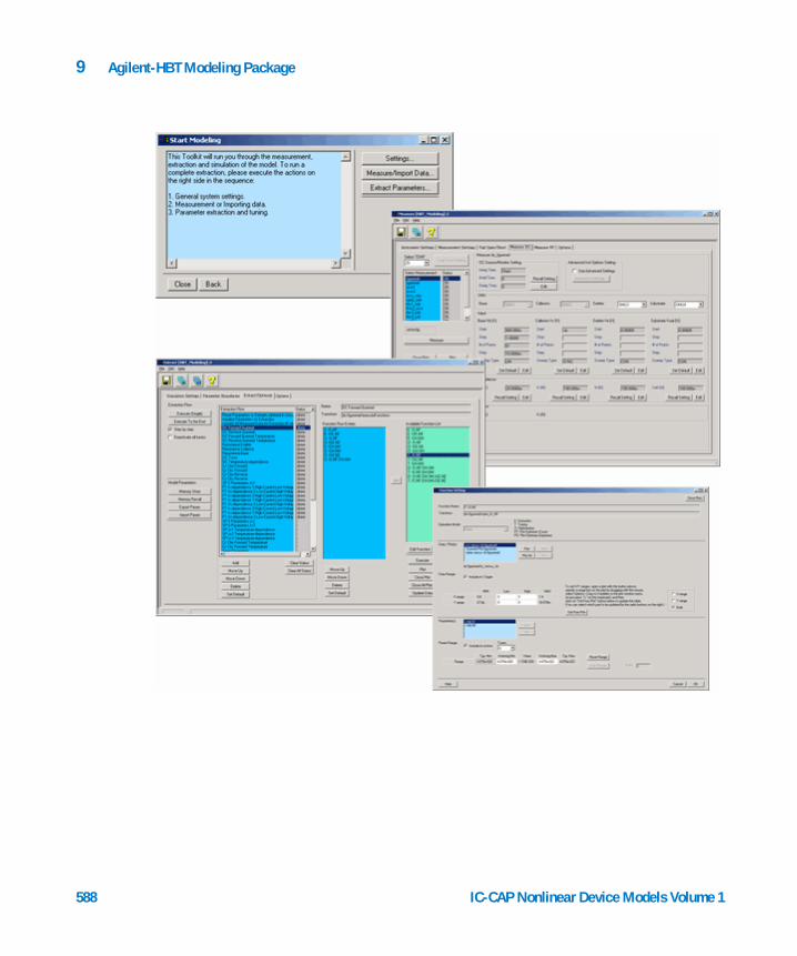
9 Agilent-HBT Modeling Package
588 IC-CAP Nonlinear Device Models Volume 1
Agilent-HBT Modeling Package 9
Key Features of the Agilent-HBT Modeling Package
IC-CAP Nonlinear Device Models Vo
• The new graphical user interface (GUI) in IC-CAP enables quick setup of measurements followed by automatic parameter extraction routines.
• The GUI contains tabbed folders that are ordered from left to right according to the task flow in the measurements and extractions, which makes the interface intuitive.
• Global settings enable quick and certain setup in measurements.
• Data management functionality enables flexible handling of measurement data.
• De-embedding process and data sets used for de-embedding are intuitively controlled by a newly introduced concept—De-embedding Sets.
• Recommended measurement setups and extraction procedures are included for effective HBT modeling.
• Powerful extraction flow edit capability and the new Function Editor enables you to customize your original extraction routines for different processes.
• The Multiplot feature enables you to view both measured and simulated plots in one window. The user-configurable plot display window (Extraction Result Browser) enables quick review of extraction results.
Before You Begin
Requirements
• The modeling package works in IC-CAP 2006 with the add-on enhancement.
• Display size must be 1024 x 768 or higher.
• Other system requirements follow those listed in the Installation and Customization Guide, Check the System Requirements” section for each operating system.
lume 1 589
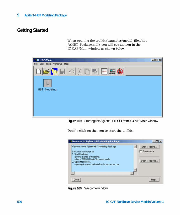
9 Agilent-HBT Modeling Package
Getting Started
590
When opening the toolkit (examples/model_files/hbt /AHBT_Package.mdl), you will see an icon in the IC-CAP/Main window as shown below.
Double-click on the icon to start the toolkit.
Figure 159 Starting the Agilent-HBT GUI from IC-CAP/Main window
Figure 160 Welcome window
IC-CAP Nonlinear Device Models Volume 1
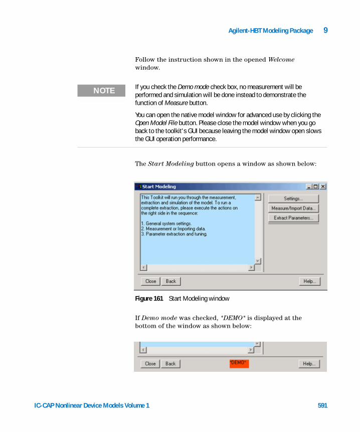
Agilent-HBT Modeling Package 9
IC-CAP Nonlinear Device Models Vo
Follow the instruction shown in the opened Welcome window.
NOTE If you check the Demo mode check box, no measurement will be performed and simulation will be done instead to demonstrate the function of Measure button.
You can open the native model window for advanced use by clicking the Open Model File button. Please close the model window when you go back to the toolkit's GUI because leaving the model window open slows the GUI operation performance.
The Start Modeling button opens a window as shown below:
If Demo mode was checked, *DEMO* is displayed at the bottom of the window as shown below:
Figure 161 Start Modeling window
lume 1 591
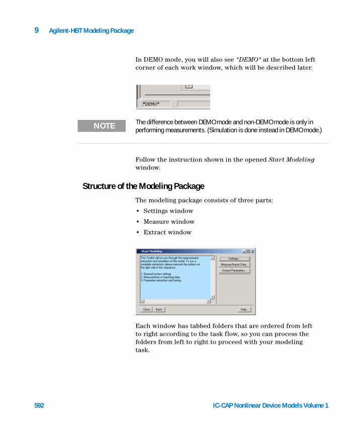
592
9 Agilent-HBT Modeling Package
In DEMO mode, you will also see *DEMO* at the bottom left corner of each work window, which will be described later.
NOTE The difference between DEMO mode and non-DEMO mode is only in performing measurements. (Simulation is done instead in DEMO mode.)
Follow the instruction shown in the opened Start Modeling window.
Structure of the Modeling Package
The modeling package consists of three parts:
• Settings window
• Measure window
• Extract window
Each window has tabbed folders that are ordered from left to right according to the task flow, so you can process the folders from left to right to proceed with your modeling task.
IC-CAP Nonlinear Device Models Volume 1

Agilent-HBT Modeling Package 9
IC-CAP Nonlinear Device Models Vo
Figure 162 Settings window
Figure 163 Measure window
lume 1 593
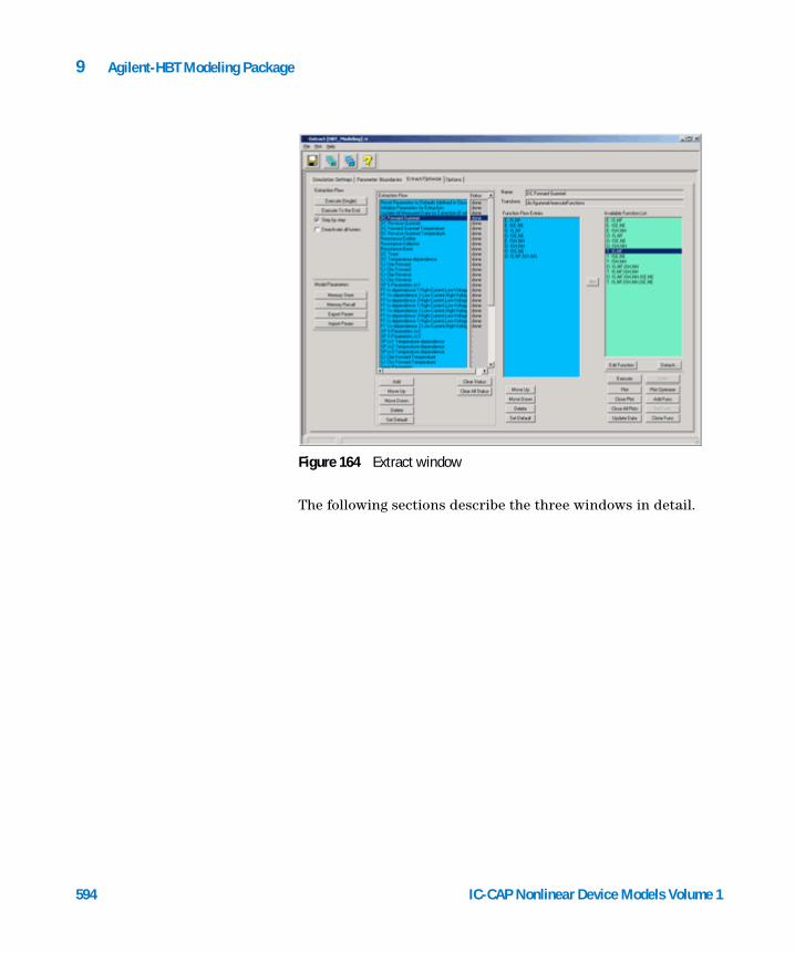
594
9 Agilent-HBT Modeling Package
The following sections describe the three windows in detail.
Figure 164 Extract window
IC-CAP Nonlinear Device Models Volume 1

Agilent-HBT Modeling Package 9
Settings Window
IC-CAP Nonlinear Device Models Vo
The Settings window consists of the following three tabbed folders:
• Information
• Device Settings
• General Settings/Options
Information
Information and notes can be entered and stored for the specific project in this folder.
lume 1 595
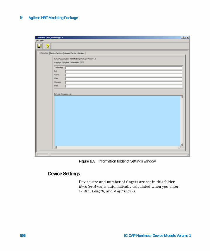
596
9 Agilent-HBT Modeling Package
Figure 165 Information folder of Settings window
Device Settings
Device size and number of fingers are set in this folder. Emitter Area is automatically calculated when you enter Width, Length, and # of Fingers.
IC-CAP Nonlinear Device Models Volume 1
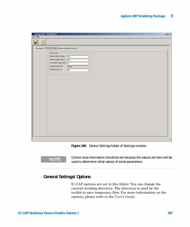
Agilent-HBT Modeling Package 9
IC-CAP Nonlinear Device Models Vo
Figure 166 Device Settings folder of Settings window
General Settings/Options
NOTE Correct area information should be set because the values set here will be used to determine initial values of some parameters.
IC-CAP options are set in this folder. You can change the current working directory. The directory is used by the toolkit to save temporary files. For more information on the options, please refer to the User's Guide.
lume 1 597
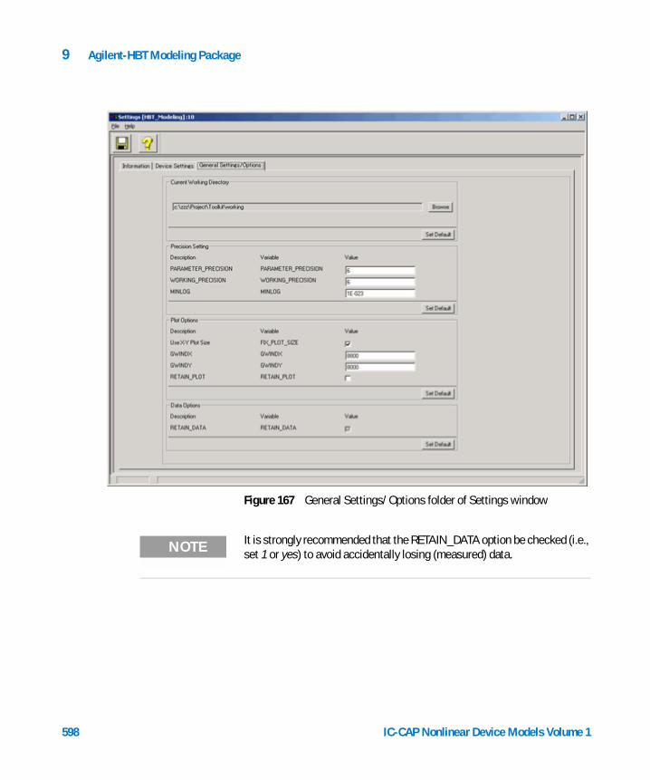
598
9 Agilent-HBT Modeling Package
Figure 167 General Settings/Options folder of Settings window
NOTE It is strongly recommended that the RETAIN_DATA option be checked (i.e., set 1 or yes) to avoid accidentally losing (measured) data.
IC-CAP Nonlinear Device Models Volume 1

Agilent-HBT Modeling Package 9
Measure Window
IC-CAP Nonlinear Device Models Vo
The Measure window consists of the following six tabbed folders:
• Instrument Settings
• Measurement Settings
• Pad Open/Short
• Measure DC
• Measure RF
• Options
Instrument Settings
Before you start measurements, you need to do some setup. Settings in this folder are Global Settings that can be referred from each measurement setups described later.
Follow the instruction shown on the left of the folder.
lume 1 599
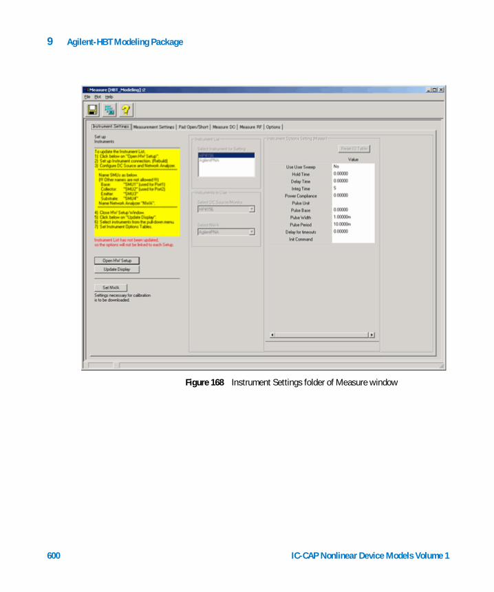
600
9 Agilent-HBT Modeling Package
Figure 168 Instrument Settings folder of Measure window
IC-CAP Nonlinear Device Models Volume 1
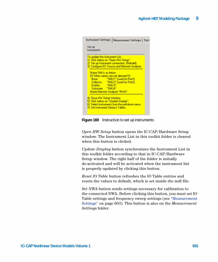
Agilent-HBT Modeling Package 9
IC-CAP Nonlinear Device Models Vo
Open HW Setup button opens the IC-CAP/Hardware Setup window. The Instrument List in this toolkit folder is cleared when this button is clicked.Update Display button synchronizes the Instrument List in this toolkit folder according to that in IC-CAP/Hardware Setup window. The right half of the folder is initially de-activated and will be activated when the instrument list is properly updated by clicking this button.
Reset IO Table button refreshes the IO Table entries and resets the values to default, which is set inside the mdl file.
Set NWA button sends settings necessary for calibration to the connected NWA. Before clicking this button, you must set IO Table settings and frequency sweep settings (see “Measurement Settings” on page 603). This button is also on the Measurement Settings folder.
Figure 169 Instruction to set up instruments
lume 1 601
9 Agilent-HBT Modeling Package
NOTE Connect instruments first. Please refer to "Making Measurements" in the IC-CAP User's Manual.
The toolkit supports only dc sources (or dc parameter analyzers) and network analyzers that IC-CAP supports.
The SMU names must be configured by SMU1, SMU2, (SMU3, SMU4, if necessary) to have the toolkit work properly. These names are required to be set in the IC-CAP/Hardware Setup window before editing any IO Tables in the toolkit.
The network analyzer name must be configured by NWA, otherwise the toolkit will not work properly.
If you get instrument option errors, check the SMU name configuration first. If the errors are still appearing after correctly setting up the SMU names, the Reset IO Table button may resolve the problem.
602
Set frequency sweep in the next Measurement Settings folder before clicking on Set NWA button.
The instrument options set in this folder are used as master (default) settings in each measurement setup. Integ Time, Hold Time, Delay Time, and Cal Set/State can be individually set later at each measurement in the toolkit's measurement folders (Measure DC folder and Measure RF folder).
For more information on instrument options, see "Supported Instruments" in the Reference manual.
IC-CAP Nonlinear Device Models Volume 1

Agilent-HBT Modeling Package 9
IC-CAP Nonlinear Device Models Vo
Figure 170 IC-CAP/Hardware Setup window and example of SMU name configuration
Measurement Settings
Temperatures, SMU compliances, and frequency sweep are set here as pre-set values. Settings in this folder are Global Settings that can be recalled in the following measurement folders by clicking on the Recall Setting buttons in each folder.
lume 1 603
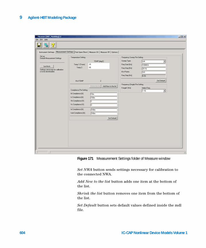
604
9 Agilent-HBT Modeling Package
Set NWA button sends settings necessary for calibration to the connected NWA.
Add New to the list button adds one item at the bottom of the list.
Shrink the list button removes one item from the bottom of the list.
Set Default button sets default values defined inside the mdl file.
Figure 171 Measurement Settings folder of Measure window
IC-CAP Nonlinear Device Models Volume 1
Agilent-HBT Modeling Package 9
Pad Open/Short
NOTE Temp1 is reserved for Tnom (room temperature).
Temp2 is usually used for High temperature, and Temp3 for Low temperature, if you have add one temperature. The minimum number of the TEMPs is 2.
IC-CAP Nonlinear Device Models Vo
Measurements of pad OPEN/SHORT are performed in this folder.
To make measurements of pads, select a Setup of Open or Short, set frequency sweep, make sure the Cal Set/State is correct, then click on the Measure button. You can recall the pre-setting (global setting) by clicking on the Recall Setting button for Cal Set/State and Recall Freq Setting button for frequency sweep. Data Names are user-definable.
lume 1 605
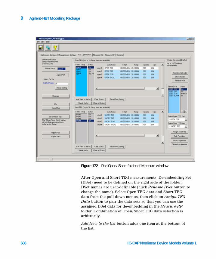
606
9 Agilent-HBT Modeling Package
After Open and Short TEG measurements, De-embedding Set (DSet) need to be defined on the right side of the folder. DSet names are user-definable (click Rename DSet button to change the name). Select Open TEG data and Short TEG data from the pull-down menus, then click on Assign TEG Data button to pair the data sets so that you can use the assigned DSet data for de-embedding in the Measure RF folder. Combination of Open/Short TEG data selection is arbitrarily.
Add New to the list button adds one item at the bottom of the list.
Figure 172 Pad Open/Short folder of Measure window
IC-CAP Nonlinear Device Models Volume 1
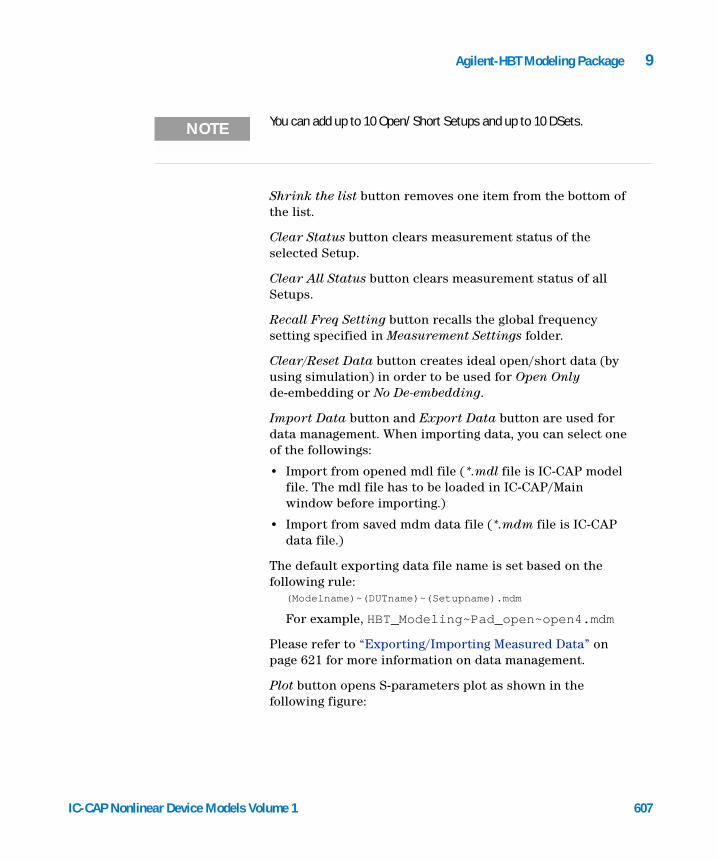
Agilent-HBT Modeling Package 9
NOTE You can add up to 10 Open/Short Setups and up to 10 DSets.
IC-CAP Nonlinear Device Models Vo
Shrink the list button removes one item from the bottom of the list.
Clear Status button clears measurement status of the selected Setup.
Clear All Status button clears measurement status of all Setups.
Recall Freq Setting button recalls the global frequency setting specified in Measurement Settings folder.
Clear/Reset Data button creates ideal open/short data (by using simulation) in order to be used for Open Only de-embedding or No De-embedding.
Import Data button and Export Data button are used for data management. When importing data, you can select one of the followings:
• Import from opened mdl file (*.mdl file is IC-CAP model file. The mdl file has to be loaded in IC-CAP/Main window before importing.)
• Import from saved mdm data file (*.mdm file is IC-CAP data file.)
The default exporting data file name is set based on the following rule:
(Modelname)~(DUTname)~(Setupname).mdm
For example, HBT_Modeling~Pad_open~open4.mdm
Please refer to “Exporting/Importing Measured Data” on page 621 for more information on data management.
Plot button opens S-parameters plot as shown in the following figure:
lume 1 607
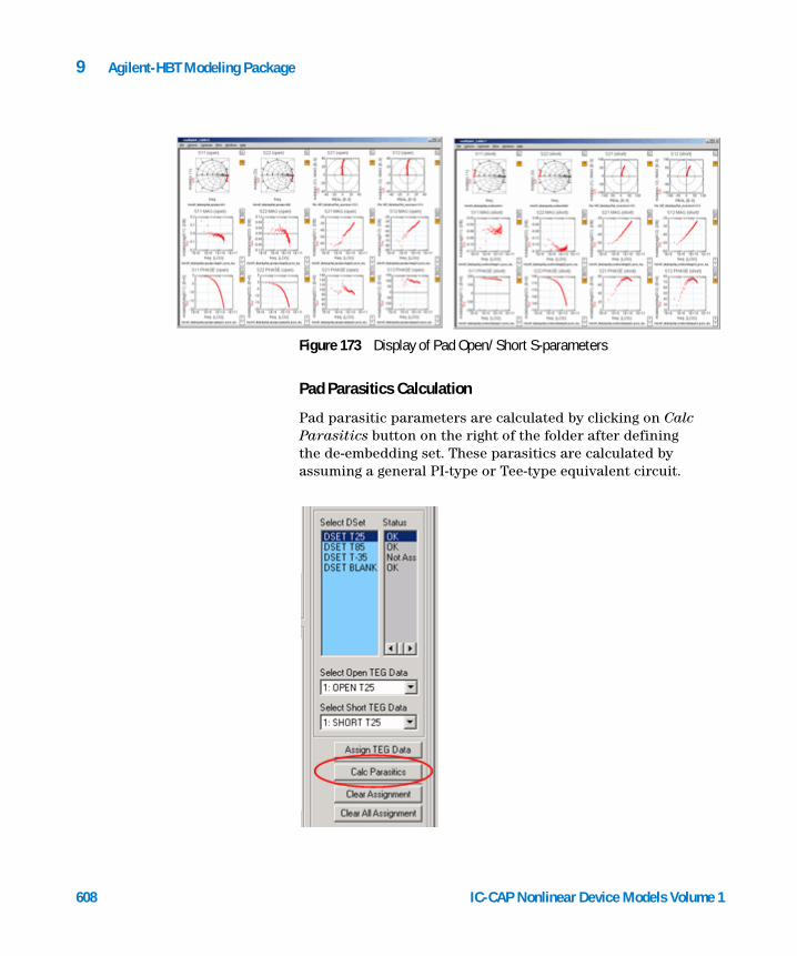
608
9 Agilent-HBT Modeling Package
Pad Parasitics Calculation
Pad parasitic parameters are calculated by clicking on Calc Parasitics button on the right of the folder after defining the de-embedding set. These parasitics are calculated by assuming a general PI-type or Tee-type equivalent circuit.
Figure 173 Display of Pad Open/Short S-parameters
IC-CAP Nonlinear Device Models Volume 1
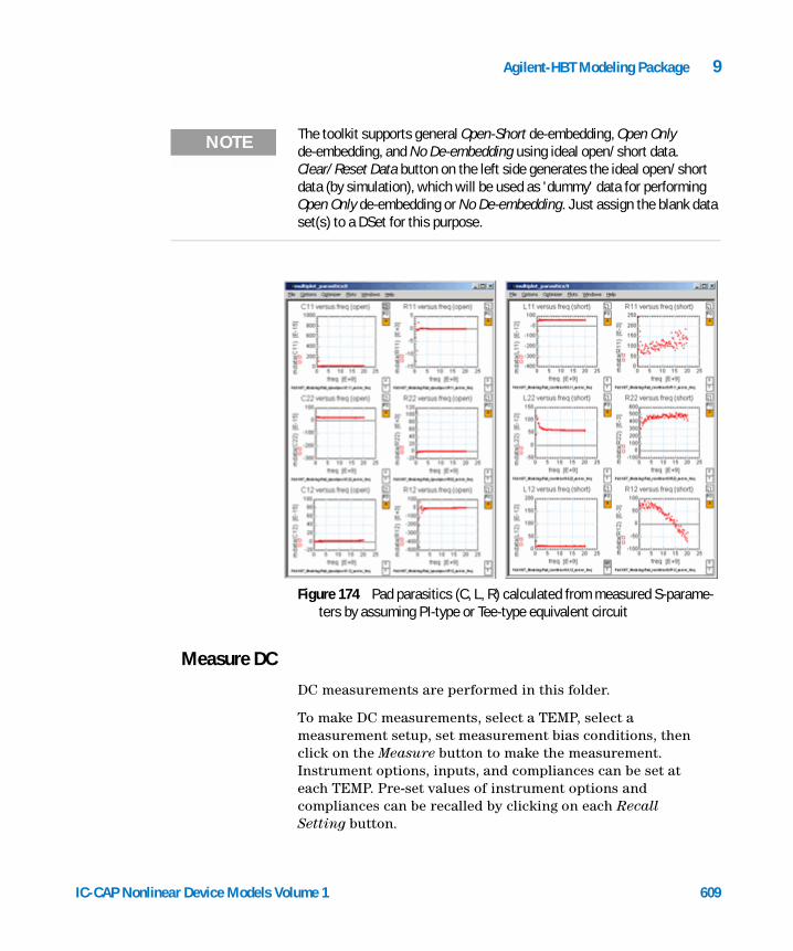
Agilent-HBT Modeling Package 9
NOTE The toolkit supports general Open-Short de-embedding, Open Only de-embedding, and No De-embedding using ideal open/short data. Clear/Reset Data button on the left side generates the ideal open/short data (by simulation), which will be used as 'dummy' data for performing Open Only de-embedding or No De-embedding. Just assign the blank data set(s) to a DSet for this purpose.
IC-CAP Nonlinear Device Models Vo
Figure 174 Pad parasitics (C, L, R) calculated from measured S-parame-ters by assuming PI-type or Tee-type equivalent circuit
Measure DC
DC measurements are performed in this folder.
To make DC measurements, select a TEMP, select a measurement setup, set measurement bias conditions, then click on the Measure button to make the measurement. Instrument options, inputs, and compliances can be set at each TEMP. Pre-set values of instrument options and compliances can be recalled by clicking on each Recall Setting button.
lume 1 609
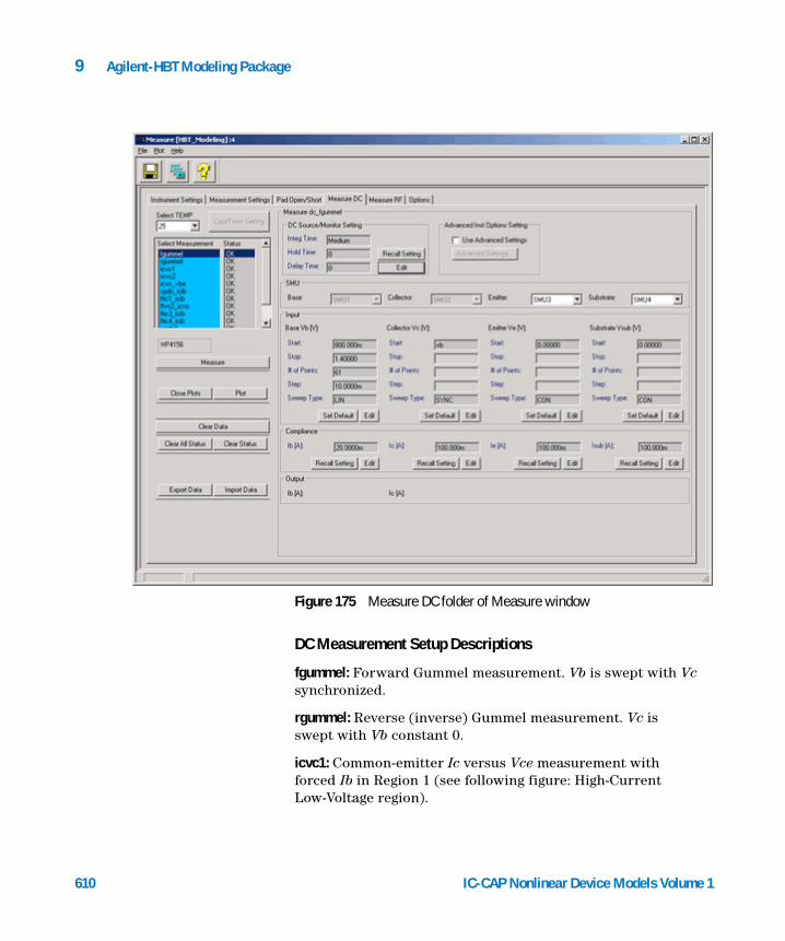
610
9 Agilent-HBT Modeling Package
DC Measurement Setup Descriptions
fgummel: Forward Gummel measurement. Vb is swept with Vc synchronized.
rgummel: Reverse (inverse) Gummel measurement. Vc is swept with Vb constant 0.
icvc1: Common-emitter Ic versus Vce measurement with forced Ib in Region 1 (see following figure: High-Current Low-Voltage region).
Figure 175 Measure DC folder of Measure window
IC-CAP Nonlinear Device Models Volume 1

Agilent-HBT Modeling Package 9
IC-CAP Nonlinear Device Models Vo
icvc2: Common-emitter Ic versus Vce measurement with forced Ib in Region 2 (see following figure: Low-Current High-Voltage region).
icvc_vbe: Common-emitter Ic versus Vce measurement with forced Vb.
spdc_icib: Ic versus Ib measurement with a constant Vc = Target Voltage. This setup is used to find bias conditions that obtain desired collector current for S-parameter measurements.
ftic1_icib: Ic versus Ib measurement with some Vc in Region 1. This setup is used to determine bias points in Region 1 at which fT will be measured in ftic1 Setup.
ftvc2_icvc: Ic versus Vce measurement with some Ib in Region 2. This setup is used to determine bias points in Region 2 at which fT will be measured in ftvc2 Setup.
ftic3_icib: Ic versus Ib measurement with some Vc in Region 3 (see following figure: region that includes high-current effects, such as Kirk effect). This setup is used to determine bias points in Region 3 at which fT will be measured in ftic3 Setup.
ftic4_icib: [Optional] Ic versus Ib measurement with some Vc in Region 4 (see following figure: Medium-Current Medium-Voltage region). This setup is used to determine bias points in Region 4 at which fT will be measured in ftic4 Setup.
lume 1 611
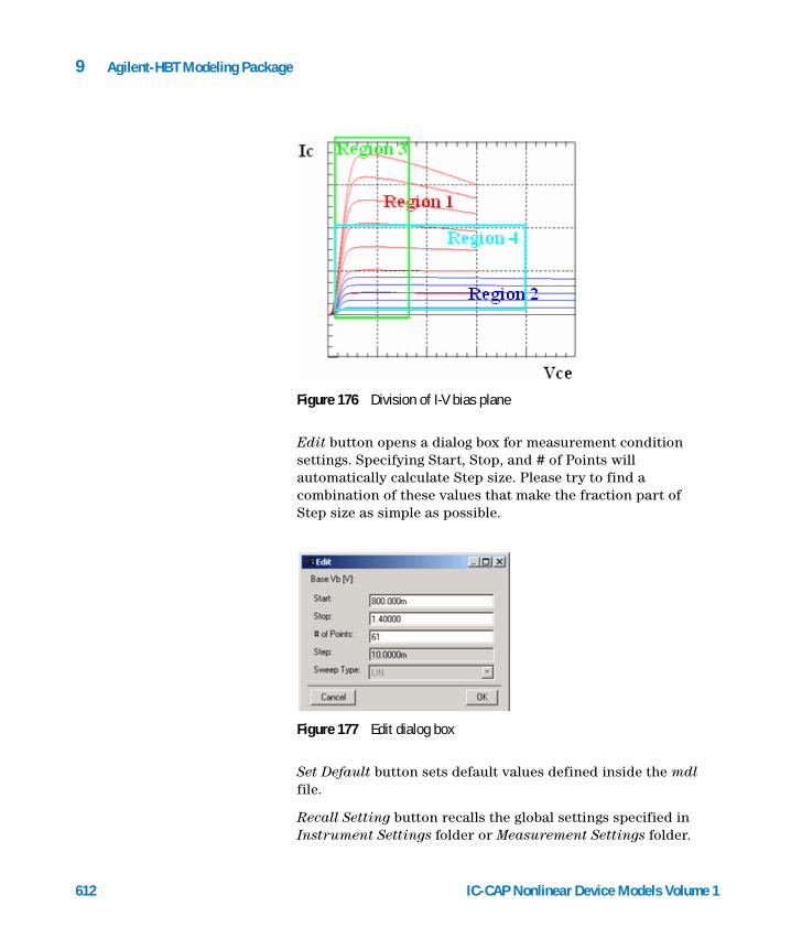
612
9 Agilent-HBT Modeling Package
Edit button opens a dialog box for measurement condition settings. Specifying Start, Stop, and # of Points will automatically calculate Step size. Please try to find a combination of these values that make the fraction part of Step size as simple as possible.
Set Default button sets default values defined inside the mdl file.
Recall Setting button recalls the global settings specified in Instrument Settings folder or Measurement Settings folder.
Figure 176 Division of I-V bias plane
Figure 177 Edit dialog box
IC-CAP Nonlinear Device Models Volume 1
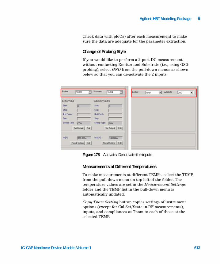
Agilent-HBT Modeling Package 9
IC-CAP Nonlinear Device Models Vo
Check data with plot(s) after each measurement to make sure the data are adequate for the parameter extraction.
Change of Probing Style
If you would like to perform a 2-port DC measurement without contacting Emitter and Substrate (i.e., using GSG probing), select GND from the pull-down menus as shown below so that you can de-activate the 2 inputs.
Measurements at Different Temperatures
To make measurements at different TEMPs, select the TEMP from the pull-down menu on top left of the folder. The temperature values are set in the Measurement Settings folder and the TEMP list in the pull-down menu is automatically updated.
Copy Tnom Setting button copies settings of instrument options (except for Cal Set/State in RF measurements), inputs, and compliances at Tnom to each of those at the selected TEMP.
Figure 178 Activate/Deactivate the inputs
lume 1 613
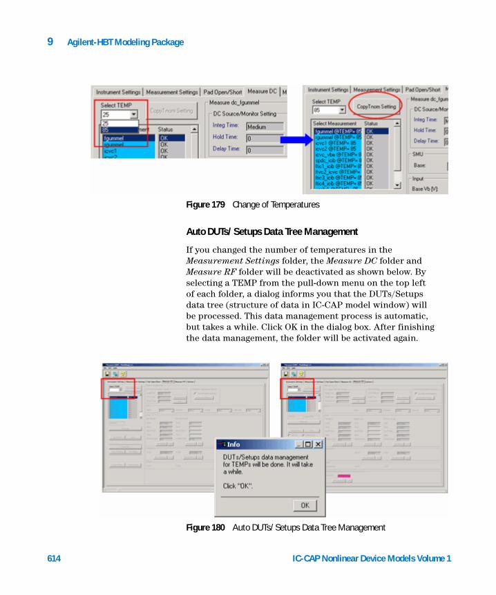
614
9 Agilent-HBT Modeling Package
Auto DUTs/Setups Data Tree Management
If you changed the number of temperatures in the Measurement Settings folder, the Measure DC folder and Measure RF folder will be deactivated as shown below. By selecting a TEMP from the pull-down menu on the top left of each folder, a dialog informs you that the DUTs/Setups data tree (structure of data in IC-CAP model window) will be processed. This data management process is automatic, but takes a while. Click OK in the dialog box. After finishing the data management, the folder will be activated again.
Figure 179 Change of Temperatures
Figure 180 Auto DUTs/Setups Data Tree Management
IC-CAP Nonlinear Device Models Volume 1
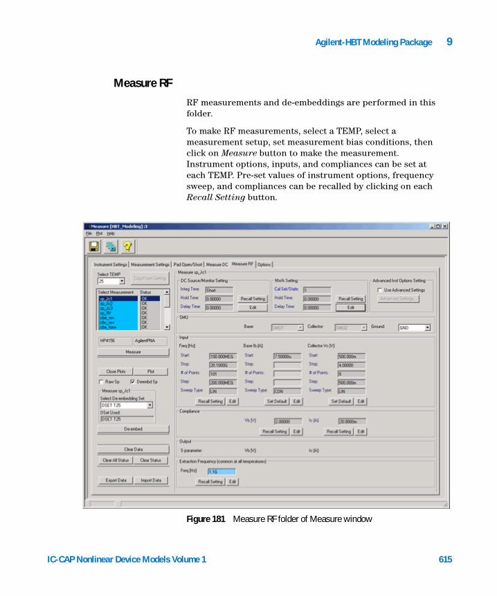
Agilent-HBT Modeling Package 9
Measure RF
IC-CAP Nonlinear Device Models Vo
RF measurements and de-embeddings are performed in this folder.
To make RF measurements, select a TEMP, select a measurement setup, set measurement bias conditions, then click on Measure button to make the measurement. Instrument options, inputs, and compliances can be set at each TEMP. Pre-set values of instrument options, frequency sweep, and compliances can be recalled by clicking on each Recall Setting button.
Figure 181 Measure RF folder of Measure window
lume 1 615
616
9 Agilent-HBT Modeling Package
RF Measurement Setup Descriptions
sp_Jc1: Frequency-swept bias-dependent S-parameter measurement in low current region. Ib is constant with Vc being swept to desired voltage.
sp_Jc2: Frequency-swept bias-dependent S-parameter measurement in medium current region. Ib is constant with Vc being swept to desired voltage.
sp_Jc3: Frequency-swept bias-dependent S-parameter measurement in high current region. Ib is constant with Vc being swept to desired voltage.
sp_0V: Frequency-swept S-parameter measurement in zero bias condition. This setup is used to obtain Cbe/Cbc/Cce versus frequency plot.
cbe_rev: One point frequency S-parameter measurement in the reverse bias region for B-E junction. This setup is used to obtain depletion capacitance Cbe versus Vb plot.
cbc_rev: One point frequency S-parameter measurement in the reverse bias region for B-C junction. This setup is used to obtain depletion capacitance Cbc versus Vc plot.
cbe_forw: One point frequency S-parameter measurement in the vicinity of the forward bias region for B-E junction. This setup is used to obtain depletion plus diffusion capacitance Cbe versus Vb plot.
cbc_forw: One point frequency S-parameter measurement in the vicinity of the forward bias region for B-C junction. This setup is used to obtain depletion plus diffusion capacitance Cbc versus Vc plot.
ftic1: One point frequency S-parameter measurement to obtain fT versus Ic at the bias points in Region 1. The bias conditions are set in the corresponding DC Setup and the conditions should be copied to this setup.
ftvc2: One point frequency S-parameter measurement to obtain fT versus Vc at the bias points in Region 2. The bias conditions are set in the corresponding DC Setup and the conditions should be copied to this setup.
IC-CAP Nonlinear Device Models Volume 1
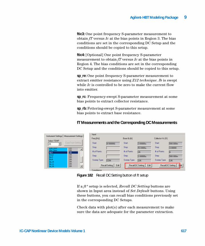
Agilent-HBT Modeling Package 9
IC-CAP Nonlinear Device Models Vo
ftic3: One point frequency S-parameter measurement to obtain fT versus Ic at the bias points in Region 3. The bias conditions are set in the corresponding DC Setup and the conditions should be copied to this setup.
ftic4: [Optional] One point frequency S-parameter measurement to obtain fT versus Ic at the bias points in Region 4. The bias conditions are set in the corresponding DC Setup and the conditions should be copied to this setup.
sp_re: One point frequency S-parameter measurement to extract emitter resistance using Z12 technique. Ib is swept while Ic is controlled to be zero to make the current flow into emitter.
sp_rc: Frequency-swept S-parameter measurement at some bias points to extract collector resistance.
sp_rb: Fettering-swept S-parameter measurement at some bias points to extract base resistance.
fT Measurements and the Corresponding DC Measurements
If a ft* setup is selected, Recall DC Setting buttons are shown in Input area instead of Set Default buttons. Using these buttons, you can recall bias conditions previously set in the corresponding DC Setups.
Check data with plot(s) after each measurement to make sure the data are adequate for the parameter extraction.
Figure 182 Recall DC Setting button of ft setup
lume 1 617
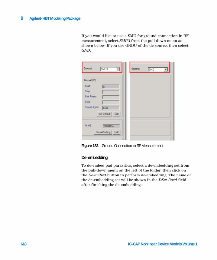
618
9 Agilent-HBT Modeling Package
If you would like to use a SMU for ground connection in RF measurement, select SMU3 from the pull-down menu as shown below. If you use GNDU of the dc source, then select GND.
De-embedding
To de-embed pad parasitics, select a de-embedding set from the pull-down menu on the left of the folder, then click on the De-embed button to perform de-embedding. The name of the de-embedding set will be shown in the DSet Used field after finishing the de-embedding.
Figure 183 Ground Connection in RF Measurement
IC-CAP Nonlinear Device Models Volume 1
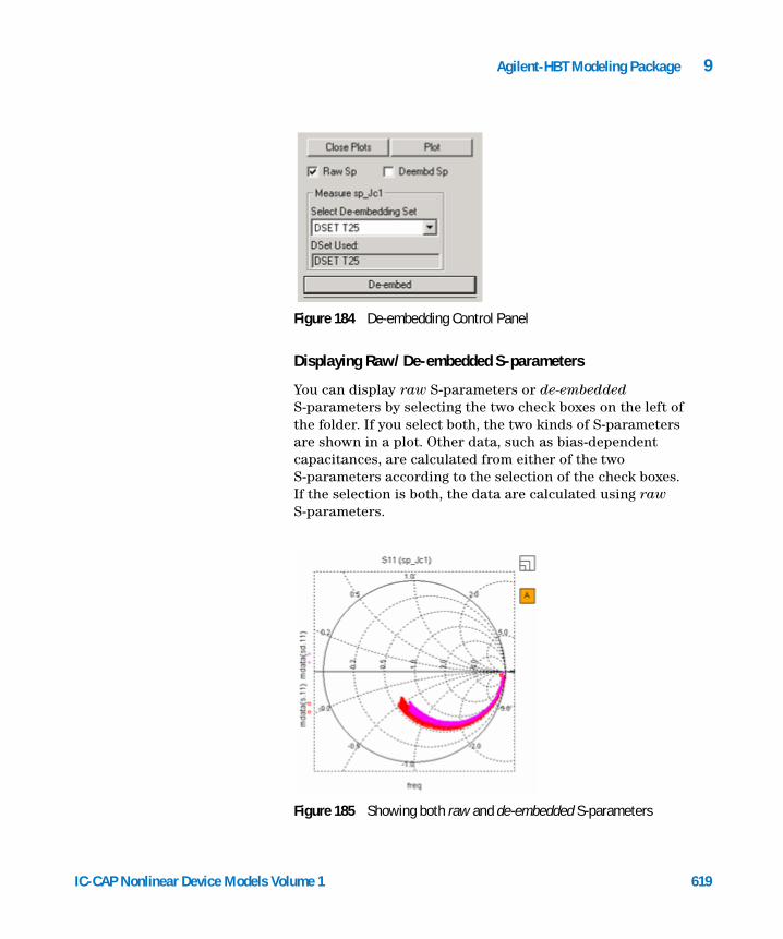
Agilent-HBT Modeling Package 9
IC-CAP Nonlinear Device Models Vo
Displaying Raw/De-embedded S-parameters
You can display raw S-parameters or de-embedded S-parameters by selecting the two check boxes on the left of the folder. If you select both, the two kinds of S-parameters are shown in a plot. Other data, such as bias-dependent capacitances, are calculated from either of the two S-parameters according to the selection of the check boxes. If the selection is both, the data are calculated using raw S-parameters.
Figure 184 De-embedding Control Panel
Figure 185 Showing both raw and de-embedded S-parameters
lume 1 619
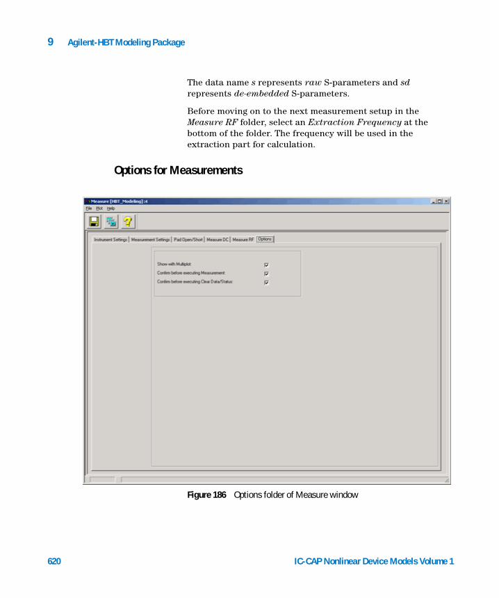
620
9 Agilent-HBT Modeling Package
The data name s represents raw S-parameters and sd represents de-embedded S-parameters.
Before moving on to the next measurement setup in the Measure RF folder, select an Extraction Frequency at the bottom of the folder. The frequency will be used in the extraction part for calculation.
Options for Measurements
Figure 186 Options folder of Measure window
IC-CAP Nonlinear Device Models Volume 1
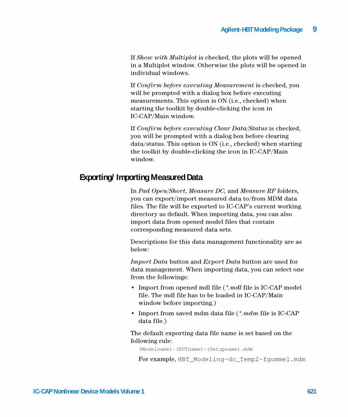
Agilent-HBT Modeling Package 9
IC-CAP Nonlinear Device Models Vo
If Show with Multiplot is checked, the plots will be opened in a Multiplot window. Otherwise the plots will be opened in individual windows.
If Confirm before executing Measurement is checked, you will be prompted with a dialog box before executing measurements. This option is ON (i.e., checked) when starting the toolkit by double-clicking the icon in IC-CAP/Main window.
If Confirm before executing Clear Data/Status is checked, you will be prompted with a dialog box before clearing data/status. This option is ON (i.e., checked) when starting the toolkit by double-clicking the icon in IC-CAP/Main window.
Exporting/Importing Measured Data
In Pad Open/Short, Measure DC, and Measure RF folders, you can export/import measured data to/from MDM data files. The file will be exported to IC-CAP’s current working directory as default. When importing data, you can also import data from opened model files that contain corresponding measured data sets.
Descriptions for this data management functionality are as below:
Import Data button and Export Data button are used for data management. When importing data, you can select one from the followings:
• Import from opened mdl file (*.mdl file is IC-CAP model file. The mdl file has to be loaded in IC-CAP/Main window before importing.)
• Import from saved mdm data file (*.mdm file is IC-CAP data file.)
The default exporting data file name is set based on the following rule:
(Modelname)~(DUTname)~(Setupname).mdm
For example, HBT_Modeling~dc_Temp2~fgummel.mdm
lume 1 621
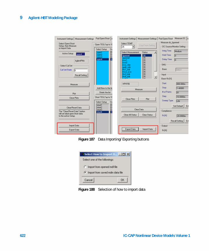
622
9 Agilent-HBT Modeling Package
Figure 187 Data Importing/Exporting buttons
Figure 188 Selection of how to import data
IC-CAP Nonlinear Device Models Volume 1

Agilent-HBT Modeling Package 9
IC-CAP Nonlinear Device Models Vo
Requirements/Limitations for Data Import
The data importing functionality has the following requirements/limitations:
• The numbers of Inputs and Outputs in the importing measured data must be the same respectively as those in the toolkit's setup to which the data are going to be imported.
• The names of Inputs/Outputs of the data must be vb, vc, ve, or vsub (for 4 nodes) for DC voltages; ib, ic (without ie and isub) for DC currents; freq for RF frequency; and s for RF S-parameters.
• Mode, Sweep Type, and Sweep Order of the Inputs/Outputs of the data must be the same respectively as those in the toolkit's setup.
• Ratio and Offset in SYNC type components must be 1.0 and 0.0 respectively.
• Value of ve or vsub with the unit of GND must be 0.0.
Figure 189 28 Selection of data in Import from opened mdl file/Import from saved mdm data file
lume 1 623
9 Agilent-HBT Modeling Package
NOTE If the IC-CAP variable of RETAIN_DATA = yes or 1, measured data will be retained when you add/remove an input/output that does not affect the data points structure. If RETAIN_DATA = no or 0, then the measured data in the setup are CLEARED. This is the nature of IC-CAP data management.
624 IC-CAP Nonlinear Device Models Volume 1
Agilent-HBT Modeling Package 9
Extract Window
IC-CAP Nonlinear Device Models Vo
The Extract window consists of the following four tabbed folders:
• Simulation Settings
• Parameter Boundaries
• Extract/Optimize
• Options
Simulation Settings
The simulator to be used (Tnom for extraction), Main Circuit, and corresponding Model Parameters are all set in this folder. The value of Tnom is automatically copied to the parameters that contain TNOM in the name.
lume 1 625
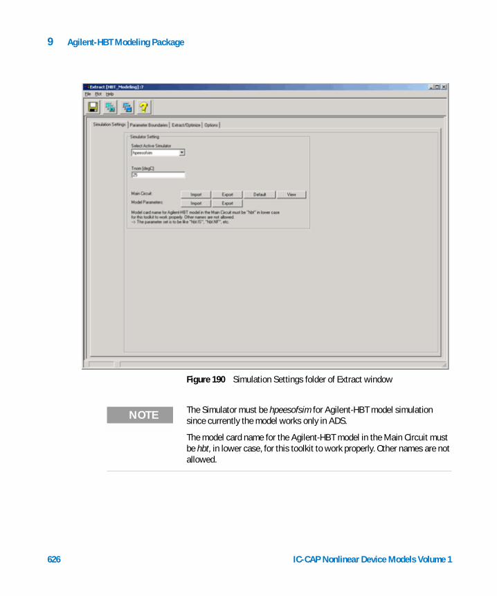
626
9 Agilent-HBT Modeling Package
Figure 190 Simulation Settings folder of Extract window
NOTE The Simulator must be hpeesofsim for Agilent-HBT model simulation since currently the model works only in ADS.
The model card name for the Agilent-HBT model in the Main Circuit must be hbt, in lower case, for this toolkit to work properly. Other names are not allowed.
IC-CAP Nonlinear Device Models Volume 1
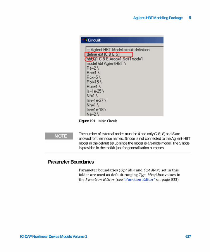
Agilent-HBT Modeling Package 9
IC-CAP Nonlinear Device Models Vo
Figure 191 Main Circuit
Parameter Boundaries
NOTE The number of external nodes must be 4 and only C, B, E, and S are allowed for their node names. S node is not connected to the Agilent-HBT model in the default setup since the model is a 3-node model. The S node is provided in the toolkit just for generalization purposes.
Parameter boundaries (Opt Min and Opt Max) set in this folder are used as default ranging Typ. Min/Max values in the Function Editor (see “Function Editor” on page 633).
lume 1 627
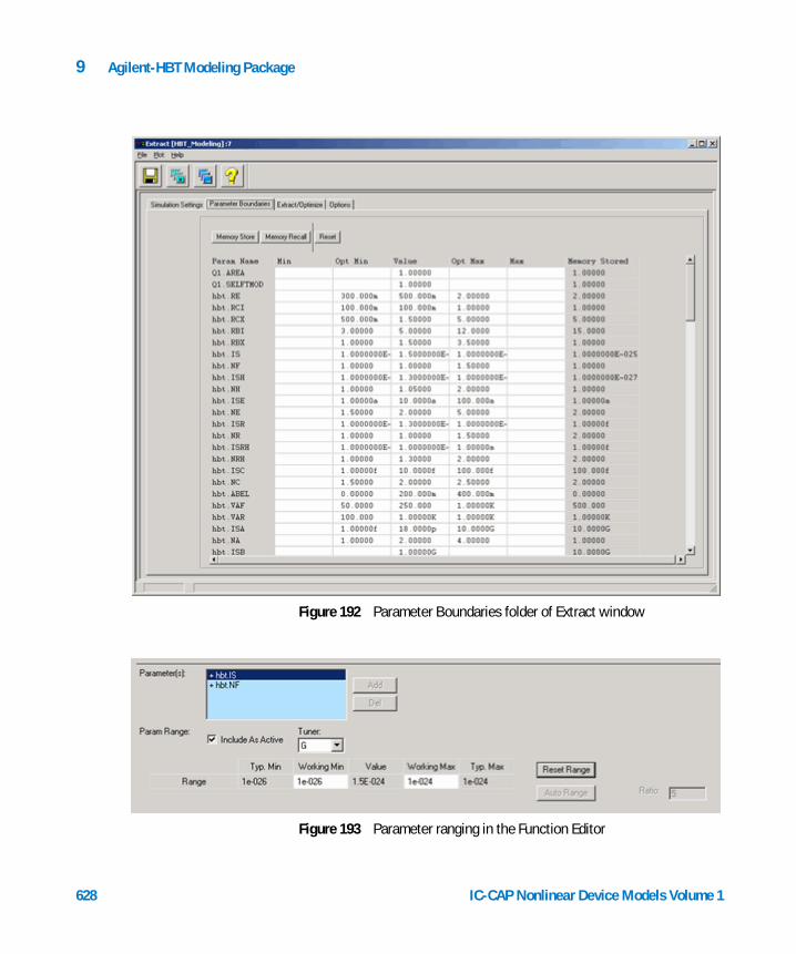
628
9 Agilent-HBT Modeling Package
Figure 192 Parameter Boundaries folder of Extract window
Figure 193 Parameter ranging in the Function Editor
IC-CAP Nonlinear Device Models Volume 1
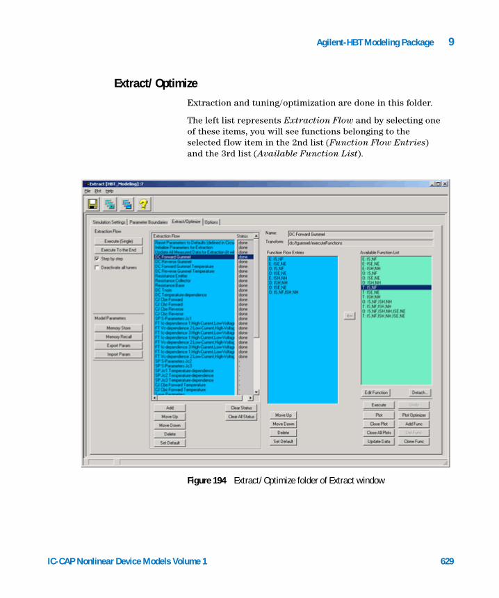
Agilent-HBT Modeling Package 9
Extract/Optimize
IC-CAP Nonlinear Device Models Vo
Extraction and tuning/optimization are done in this folder.
The left list represents Extraction Flow and by selecting one of these items, you will see functions belonging to the selected flow item in the 2nd list (Function Flow Entries) and the 3rd list (Available Function List).
Figure 194 Extract/Optimize folder of Extract window
lume 1 629
630
9 Agilent-HBT Modeling Package
Flow Execution (Group execution of functions)
Execute (Single) button executes a single flow item in which some functions are grouped and listed for execution. You can edit the function entry list with <--- button, Delete button, and Move Up/Down buttons.
Execute To the End button executes from the selected flow item to the end of the flow list. If the Step by step check box is checked, the execution will pause at each end of the flow item execution with a prompting dialog box. If Deactivate all tuners is checked, all tuning functions will be skipped during the flow execution.
IC-CAP Nonlinear Device Models Volume 1
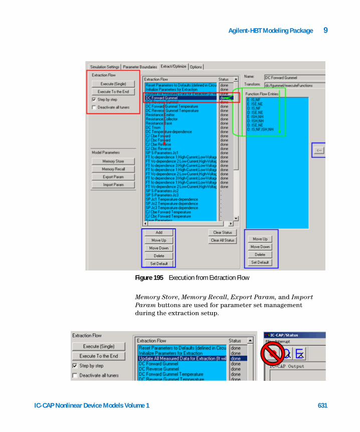
Agilent-HBT Modeling Package 9
IC-CAP Nonlinear Device Models Vo
Memory Store, Memory Recall, Export Param, and Import Param buttons are used for parameter set management during the extraction setup.
Figure 195 Execution from Extraction Flow
lume 1 631
9 Agilent-HBT Modeling Package
NOTE The flow item of Update All Measured Data for Extraction is necessary to be executed at least once before actual extraction procedures. Executing this ensures that all measured data sets are calculated (using de-embedded S-parameters for RF) and updated. This will take several minutes or so.
CAUTION DO NOT stop execution of Update All Measured Data for Extraction by pressing the RED stop sign button on the IC-CAP/Status window. Interrupting the process of updating variables and variable arrays inside the mdl file will destroy the variable structures, and in this case, you may have to reload the toolkit without saving.
632
Function Execution (Individual function execution)
Execute button below the Available Function List on the right of the folder executes the selected function in the list.
IC-CAP Nonlinear Device Models Volume 1
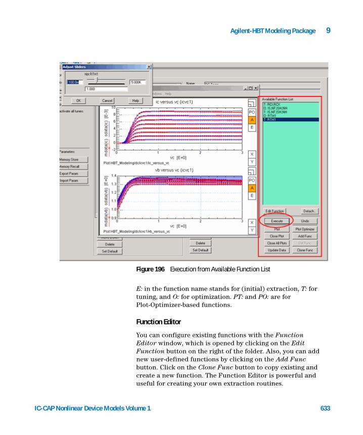
Agilent-HBT Modeling Package 9
IC-CAP Nonlinear Device Models Vo
E: in the function name stands for (initial) extraction, T: for tuning, and O: for optimization. PT: and PO: are for Plot-Optimizer-based functions.
Function Editor
You can configure existing functions with the Function Editor window, which is opened by clicking on the Edit Function button on the right of the folder. Also, you can add new user-defined functions by clicking on the Add Func button. Click on the Clone Func button to copy existing and create a new function. The Function Editor is powerful and useful for creating your own extraction routines.
Figure 196 Execution from Available Function List
lume 1 633
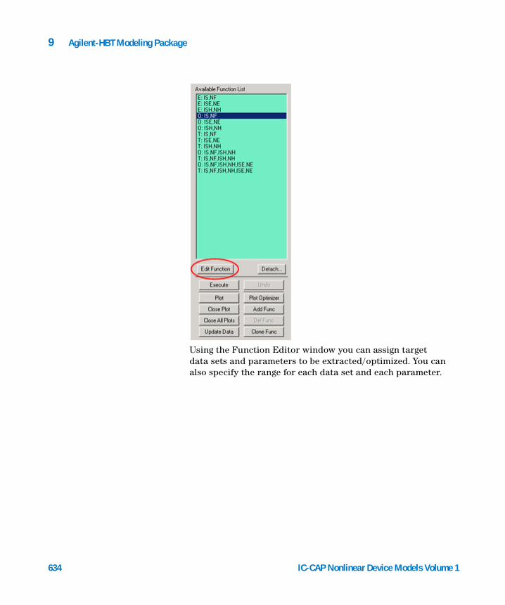
634
9 Agilent-HBT Modeling Package
Using the Function Editor window you can assign target data sets and parameters to be extracted/optimized. You can also specify the range for each data set and each parameter.
IC-CAP Nonlinear Device Models Volume 1
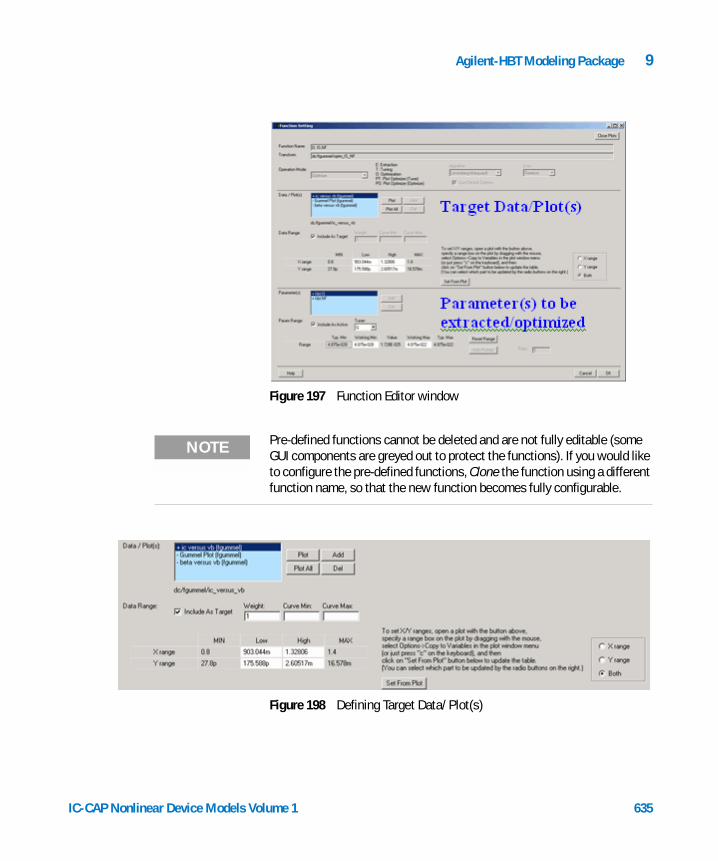
Agilent-HBT Modeling Package 9
IC-CAP Nonlinear Device Models Vo
Figure 197 Function Editor window
NOTE Pre-defined functions cannot be deleted and are not fully editable (some GUI components are greyed out to protect the functions). If you would like to configure the pre-defined functions, Clone the function using a different function name, so that the new function becomes fully configurable.Figure 198 Defining Target Data/Plot(s)
lume 1 635
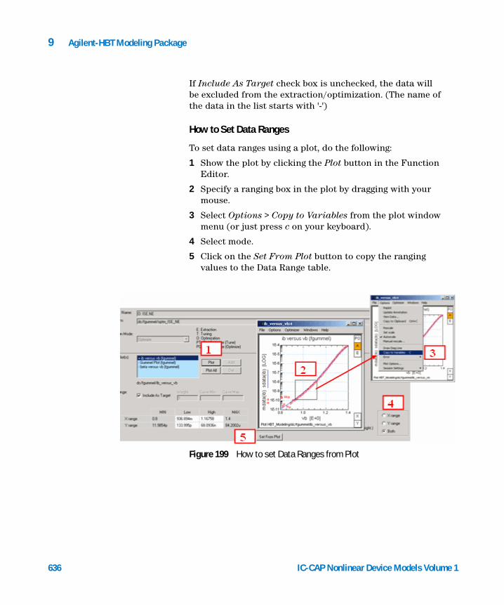
636
9 Agilent-HBT Modeling Package
If Include As Target check box is unchecked, the data will be excluded from the extraction/optimization. (The name of the data in the list starts with '-')
How to Set Data Ranges
To set data ranges using a plot, do the following:
1 Show the plot by clicking the Plot button in the Function Editor.
2 Specify a ranging box in the plot by dragging with your mouse.
3 Select Options > Copy to Variables from the plot window menu (or just press c on your keyboard).
4 Select mode.
5 Click on the Set From Plot button to copy the ranging values to the Data Range table.
Figure 199 How to set Data Ranges from Plot
IC-CAP Nonlinear Device Models Volume 1
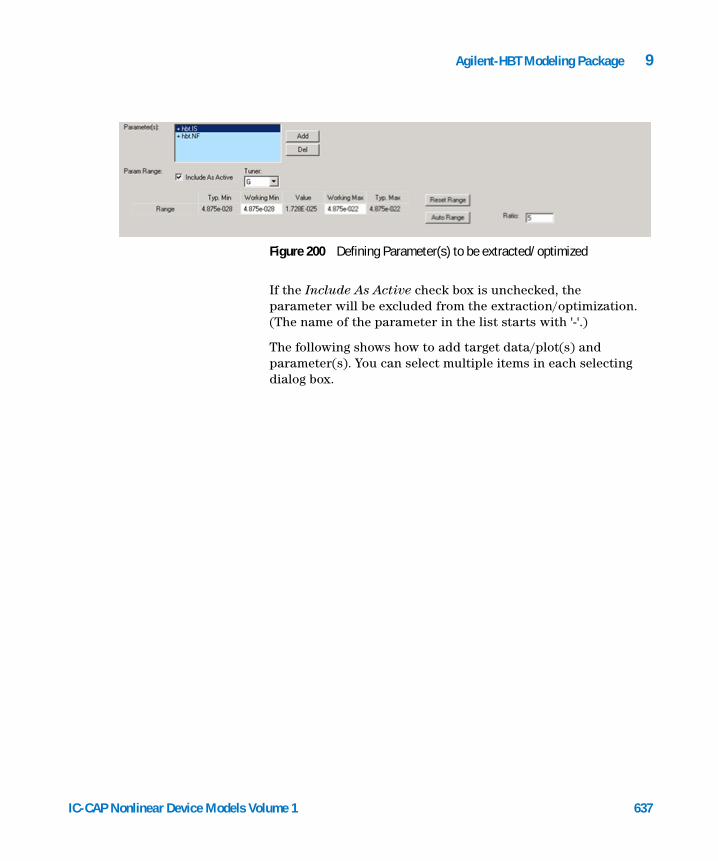
Agilent-HBT Modeling Package 9
IC-CAP Nonlinear Device Models Vo
If the Include As Active check box is unchecked, the parameter will be excluded from the extraction/optimization. (The name of the parameter in the list starts with '-'.)
The following shows how to add target data/plot(s) and parameter(s). You can select multiple items in each selecting dialog box.
Figure 200 Defining Parameter(s) to be extracted/optimized
lume 1 637
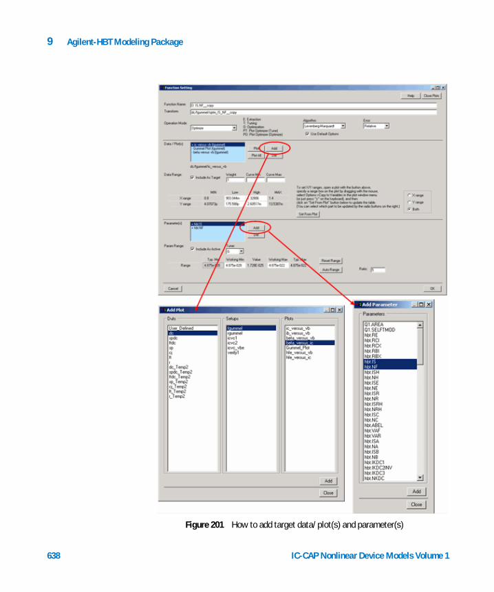
638
9 Agilent-HBT Modeling Package
Figure 201 How to add target data/plot(s) and parameter(s)
IC-CAP Nonlinear Device Models Volume 1
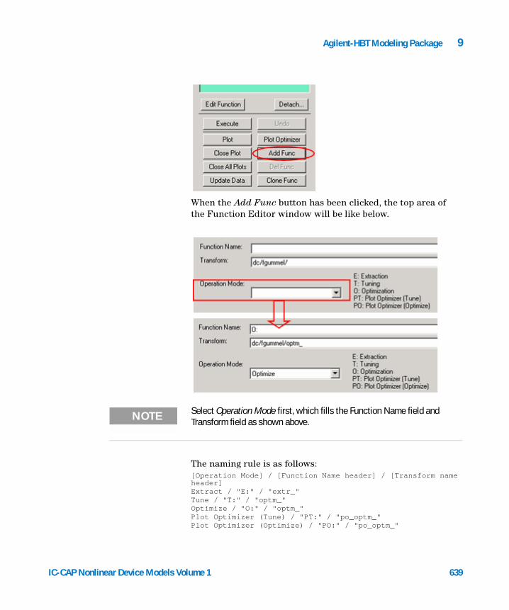
Agilent-HBT Modeling Package 9
IC-CAP Nonlinear Device Models Vo
When the Add Func button has been clicked, the top area of the Function Editor window will be like below.
NOTE Select Operation Mode first, which fills the Function Name field and Transform field as shown above.
The naming rule is as follows:[Operation Mode] / [Function Name header] / [Transform name header]Extract / "E:" / "extr_"Tune / "T:" / "optm_"Optimize / "O:" / "optm_"Plot Optimizer (Tune) / "PT:" / "po_optm_"Plot Optimizer (Optimize) / "PO:" / "po_optm_"
lume 1 639
640
9 Agilent-HBT Modeling Package
To avoid needless confusion you should follow the naming rule for the Function name and Transform name.
NOTE For the Transform name, only alphabetic characters, numbers providing they are not the first character, and "_" (under bar) are allowed. DO NOT use any other characters.
When the Clone Func button has been clicked, the top area of the Function Editor window will be like below.
The cloned function of a pre-defined function is fully configurable.
IC-CAP Nonlinear Device Models Volume 1
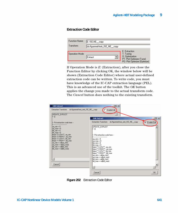
Agilent-HBT Modeling Package 9
IC-CAP Nonlinear Device Models Vo
Extraction Code Editor
If Operation Mode is E: (Extraction), after you close the Function Editor by clicking OK, the window below will be shown (Extraction Code Editor) where actual user-defined extraction code can be written. To write code, you must have knowledge of the IC-CAP extraction language (PEL). This is an advanced use of the toolkit. The OK button applies the change you made to the actual transform code. The Cancel button does nothing to the existing transform.
Figure 202 Extraction Code Editor
lume 1 641
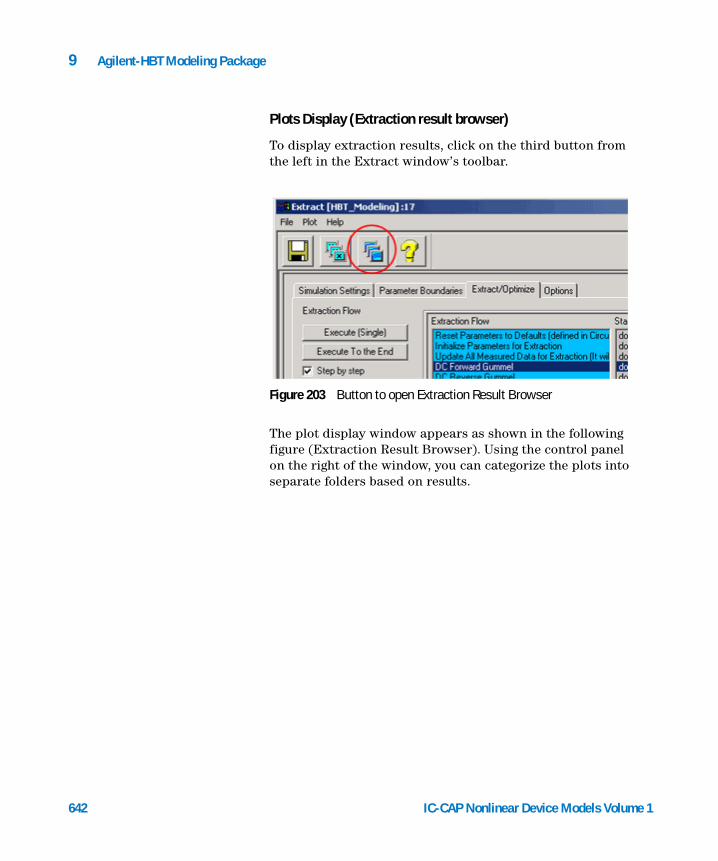
642
9 Agilent-HBT Modeling Package
Plots Display (Extraction result browser)
To display extraction results, click on the third button from the left in the Extract window’s toolbar.
The plot display window appears as shown in the following figure (Extraction Result Browser). Using the control panel on the right of the window, you can categorize the plots into separate folders based on results.
Figure 203 Button to open Extraction Result Browser
IC-CAP Nonlinear Device Models Volume 1
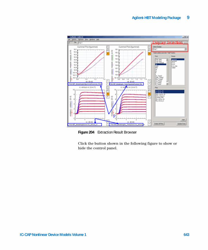
Agilent-HBT Modeling Package 9
IC-CAP Nonlinear Device Models Vo
Click the button shown in the following figure to show or hide the control panel.
Figure 204 Extraction Result Browser
lume 1 643
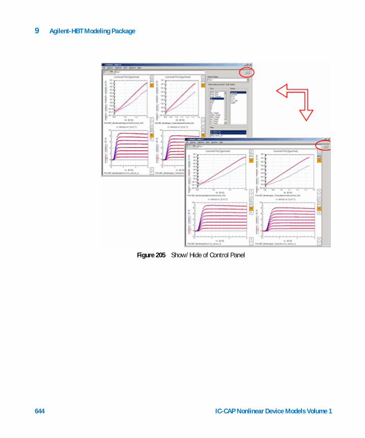
644
9 Agilent-HBT Modeling Package
Figure 205 Show/Hide of Control Panel
IC-CAP Nonlinear Device Models Volume 1
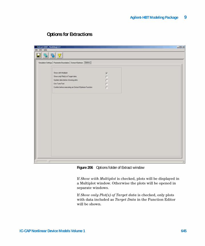
Agilent-HBT Modeling Package 9
Options for Extractions
IC-CAP Nonlinear Device Models Vo
If Show with Multiplot is checked, plots will be displayed in a Multiplot window. Otherwise the plots will be opened in separate windows.
If Show only Plot(s) of Target data is checked, only plots with data included as Target Data in the Function Editor will be shown.
Figure 206 Options folder of Extract window
lume 1 645
646
9 Agilent-HBT Modeling Package
If Update data before showing plots is checked, the data is updated before plots are displayed. Otherwise, plots are shown quickly without updating the data.
If Use Tune Fast is checked, Tune functions are executed in Fast mode.
If Confirm before executing an Extract/Optimize Function is checked, you will be prompted with a dialog box before executing each function.
IC-CAP Nonlinear Device Models Volume 1
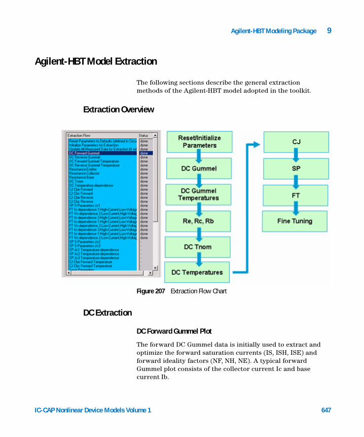
Agilent-HBT Modeling Package 9
Agilent-HBT Model Extraction
IC-CAP Nonlinear Device Models Vo
The following sections describe the general extraction methods of the Agilent-HBT model adopted in the toolkit.
Extraction Overview
Figure 207 Extraction Flow Chart
DC Extraction
DC Forward Gummel Plot
The forward DC Gummel data is initially used to extract and optimize the forward saturation currents (IS, ISH, ISE) and forward ideality factors (NF, NH, NE). A typical forward Gummel plot consists of the collector current Ic and base current Ib.
lume 1 647
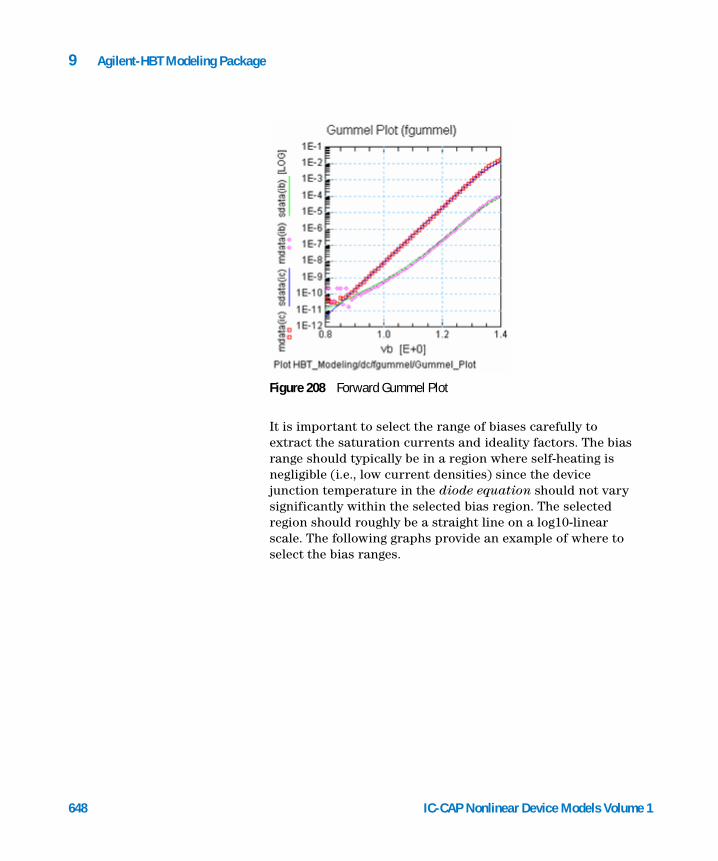
648
9 Agilent-HBT Modeling Package
It is important to select the range of biases carefully toextract the saturation currents and ideality factors. The bias range should typically be in a region where self-heating is negligible (i.e., low current densities) since the device junction temperature in the diode equation should not vary significantly within the selected bias region. The selected region should roughly be a straight line on a log10-linear scale. The following graphs provide an example of where to select the bias ranges.
Figure 208 Forward Gummel Plot
IC-CAP Nonlinear Device Models Volume 1
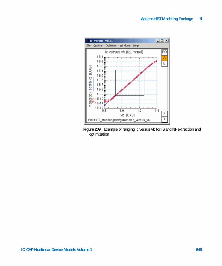
Agilent-HBT Modeling Package 9
IC-CAP Nonlinear Device Models Vo
Figure 209 Example of ranging Ic versus Vb for IS and NF extraction and optimization
lume 1 649
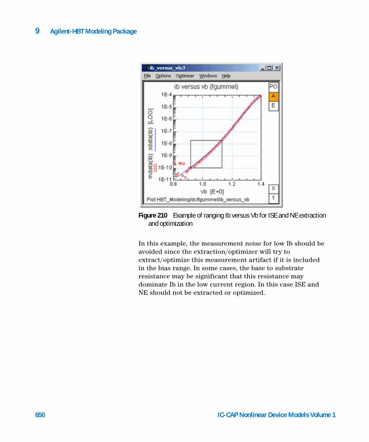
650
9 Agilent-HBT Modeling Package
In this example, the measurement noise for low Ib should be avoided since the extraction/optimizer will try to extract/optimize this measurement artifact if it is included in the bias range. In some cases, the base to substrate resistance may be significant that this resistance may dominate Ib in the low current region. In this case ISE and NE should not be extracted or optimized.
Figure 210 Example of ranging Ib versus Vb for ISE and NE extraction and optimization
IC-CAP Nonlinear Device Models Volume 1
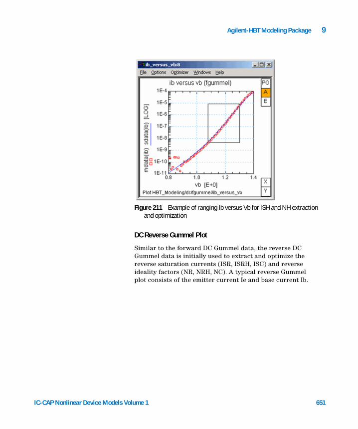
Agilent-HBT Modeling Package 9
IC-CAP Nonlinear Device Models Vo
DC Reverse Gummel Plot
Similar to the forward DC Gummel data, the reverse DC Gummel data is initially used to extract and optimize the reverse saturation currents (ISR, ISRH, ISC) and reverse ideality factors (NR, NRH, NC). A typical reverse Gummel plot consists of the emitter current Ie and base current Ib.
Figure 211 Example of ranging Ib versus Vb for ISH and NH extraction and optimization
lume 1 651
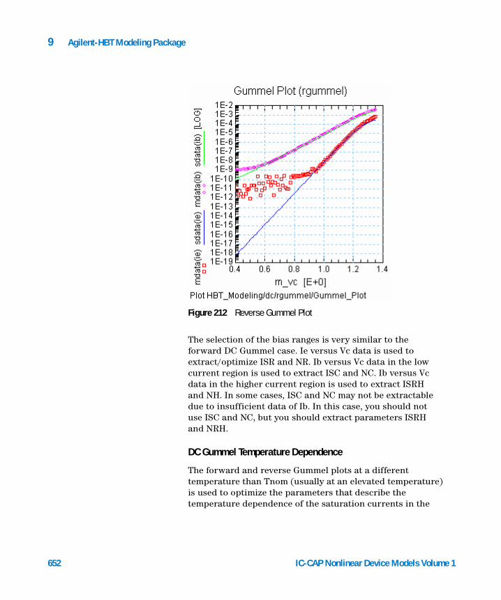
652
9 Agilent-HBT Modeling Package
The selection of the bias ranges is very similar to the forward DC Gummel case. Ie versus Vc data is used to extract/optimize ISR and NR. Ib versus Vc data in the low current region is used to extract ISC and NC. Ib versus Vc data in the higher current region is used to extract ISRH and NH. In some cases, ISC and NC may not be extractable due to insufficient data of Ib. In this case, you should not use ISC and NC, but you should extract parameters ISRH and NRH.
DC Gummel Temperature Dependence
The forward and reverse Gummel plots at a different temperature than Tnom (usually at an elevated temperature) is used to optimize the parameters that describe the temperature dependence of the saturation currents in the
Figure 212 Reverse Gummel Plot
IC-CAP Nonlinear Device Models Volume 1
Agilent-HBT Modeling Package 9
IC-CAP Nonlinear Device Models Vo
diode equation. The following list describes how the temperature parameters are related to the Tnom saturation current parameters:
XTIS <--> IS
XTIH <--> ISH
XTIE <--> ISE
XTIR <--> ISR
XTIRH <--> ISRH
XTIC <--> ISC
These parameters describe the temperature scaling of the DC saturation currents, and so they should be optimized in a region where self-heating is not significant (i.e., device junction temperature should be constant within the bias region).
DC I-V
Ic versus Vce plot is used to fine-tune the diode equation parameters in the area of relative low power dissipation (i.e., minimal self-heating).
lume 1 653
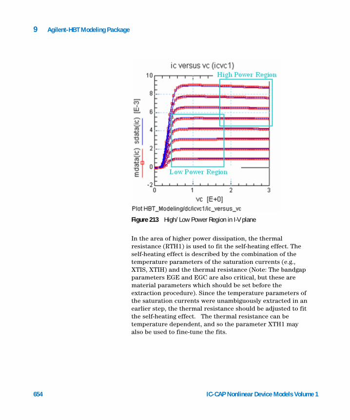
654
9 Agilent-HBT Modeling Package
In the area of higher power dissipation, the thermal resistance (RTH1) is used to fit the self-heating effect. The self-heating effect is described by the combination of the temperature parameters of the saturation currents (e.g., XTIS, XTIH) and the thermal resistance (Note: The bandgap parameters EGE and EGC are also critical, but these are material parameters which should be set before the extraction procedure). Since the temperature parameters of the saturation currents were unambiguously extracted in an earlier step, the thermal resistance should be adjusted to fit the self-heating effect. The thermal resistance can be temperature dependent, and so the parameter XTH1 may also be used to fine-tune the fits.
Figure 213 High/Low Power Region in I-V plane
IC-CAP Nonlinear Device Models Volume 1
Agilent-HBT Modeling Package 9
R Extraction
IC-CAP Nonlinear Device Models Vo
In general, the device resistances are extracted from network analyzer measurements. Although it is possible to extract an estimate of the device resistances solely from DC measurements, self-heating effects typically cloud the actual values of the device resistance. Since the resistances are usually sensed with significant current through them, it is only natural that the device experiences significant self-heating, which then affects the accuracy of the resistances if extracted from the derivatives of the DC I-V characteristics.
Emitter Resistance
The Real(Z12) method is used to extract the emitter resistance, RE. The real part of Z12 measured at low RF frequencies consists of the constant emitter resistance (RE) and the dynamic junction resistance, which is current dependent. By extrapolating to infinite current (by measuring S-parameters at various collector currents), the constant emitter resistance can be extracted.
Collector Resistance
The total collector resistance is extracted by biasing the collector voltage at Vce=0, sweeping Vbe in forward bias, and calculating from S-parameters measured over frequency. Most of the extracted collector resistance is partitioned to RCX (Extrinsic collector resistance). As a default, 5% of the total collector resistance is allocated to RCI (Intrinsic collector resistance).
Base Resistance
The total base resistance is extracted by biasing the collector voltage at Vce=1V, sweeping Vbe in forward bias, and calculating from S-parameters measured over frequency. The calculation assumes the emitter resistance (RE) is extracted beforehand. This is critical for small area devices where the emitter resistance can be a comparable in magnitude to the base resistance. The default partitioning between RBI
lume 1 655
656
9 Agilent-HBT Modeling Package
(Intrinsic base resistance) and RBX (Extrinsic base resistance) is set at 80/20 where RBI gets 80% of the total base resistance. This partitioning of the base resistance between RBI and RBX is important for accurate high frequency operation (e.g. fmax, MSG, S12, S22, etc), and the fine-tuning of these parameters is done at a later step.
CJ Extraction
Both Cbe and Cbc are extracted using a similar method. Parameters CJx, VJx, and CxMAX (where x="E" or "C") are initially extracted from measured data. Then the forward bias data are used to optimize the aforementioned parameters in addition to MJx. Finally, the reverse bias data are used to optimize the punch-through capacitance parameters VTPx and MJxR.
SP Extraction
Rb Tuning
S11 at high frequencies is used to verify the accuracy of the total base resistance extraction. A tuner can be used to tune RBI and/or RBX to make adjustments to the extracted value. The partitioning of RBI and RBX is not done at this point yet.
Re Tuning
S21 at low frequencies is used to verify the accuracy of the extracted emitter resistance. A tuner can be used to fine-tine RE to make adjustments to the extracted value.
FT Extraction
The total transit time is related to fT by the expression:
By this point of the extraction it is assumed that the parameters associated with resistances Rc and Re and capacitance Cbc are extracted properly. The only parameter that is not extracted precisely is CEMAX (Cbe near forward
IC-CAP Nonlinear Device Models Volume 1
Agilent-HBT Modeling Package 9
IC-CAP Nonlinear Device Models Vo
bias), and so this parameter is optimized in more detail in the transit time parameter extraction. The rest of the fT extraction part will extract and optimize parameters associated with tauB (base transit time), tauC (collector transit time), and tauKE (Kirk effect and/or high current delay).
Ft Region 1 (ftic1)
Major parameters: TFC0, TCMIN, ITC, ITC2
This data is used to extract the initial value of the low current collector transit time parameter TFC0. To extract this parameter, you need to specify the bias region where tauC (in the equation above) starts to dominate by specifying the range like below. Also, initial values of ITC and ITC2 are extracted by examining the fT versus Ic curve for Vcb~0V. TCMIN is optimized to fit the lower current region.
lume 1 657

658
9 Agilent-HBT Modeling Package
Ft Region 2 (ftvc2)
Major parameters: VTC0INV, VTCMININV
Detailed parameters: VTR0, VMX0, VTRMIN, VMXMIN
These parameters model Vce dependence of fT. It is necessary to select bias ranges carefully to obtain a good fit.
Figure 214 Example of ranging Tau versus inverse of Ic for TFC0 extrac-tion and optimization
IC-CAP Nonlinear Device Models Volume 1
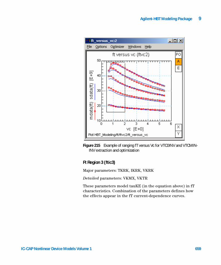
Agilent-HBT Modeling Package 9
IC-CAP Nonlinear Device Models Vo
Ft Region 3 (ftic3)
Major parameters: TKRK, IKRK, VKRK
Detailed parameters: VKMX, VKTR
These parameters model tauKE (in the equation above) in fT characteristics. Combination of the parameters defines how the effects appear in the fT current-dependence curves.
Figure 215 Example of ranging fT versus Vc for VTC0INV and VTCMIN-INV extraction and optimization
lume 1 659

660
9 Agilent-HBT Modeling Package
IC-CAP Nonlinear Device Models Volume 1
Agilent 85190A IC-CAP 2008Nonlinear Device Models Volume 1
10UCB GaAs MESFET Characterization
UCB GaAs MESFET Model 663
Simulators 664
Model Parameters 667
Test Instruments 669
Measuring and Extracting 670
Extraction Algorithms 680
References 681
This chapter describes the UCB GaAs MESFET transistor model supported by SPICE. Descriptions of model setup, instrument connections, and model parameters are included as well as test instrument information. Procedures are included for extracting AC and DC model parameters from GaAs MESFET transistors using the UCB GaAs MESFET Model. These model parameters describe the operating characteristics of the device under test (DUT) and can be derived from either simulated or direct measurements of the DUT.
The IC-CAP UCB GaAs MESFET modeling module provides setups that can be used for general measurement and model extraction for GaAs technology. The IC-CAP system offers the flexibility to modify any measurement or simulation specification.
The model extractions provided are also intended for general GaAs IC processes. If you have another method of extracting specific model parameters, you can do so with the Program function or by writing a function in C and linking it to the Function List. Details on the Program transform and writing
661Agilent Technologies
662
10 UCB GaAs MESFET Characterization
user-defined C language routines are explained in Chapter 9, “Using Transforms and Functions,” in the IC-CAP User’s Guide.
The model presented here has been enhanced with the inclusion of the series inductors and the gate resistor. Both of these are implemented as circuit elements of the overall subcircuit. This is an example of one method you might use to customize your own model.
IC-CAP Nonlinear Device Models Volume 1
UCB GaAs MESFET Characterization 10
UCB GaAs MESFET Model
IC-CAP Nonlinear Device Models Vo
The UCB GaAs MESFET model is contained in an IC-CAP example file UCBGaas.mdl. The file consists of a single level model that is based on a model developed at Raytheon and implemented in UCB’s SPICE3 simulator [1][2]. In this model, drain current is proportional to the square of the gate-to-source voltage multiplied by the expansion series of the hyperbolic tangent of the drain-to-source voltage.
The model defines total gate junction capacitance and takes into account the FET symmetry and carrier velocity saturation. Unlike the SPICE3 version, the IC-CAP model includes gate, source, and drain inductances, and gate resistance. These components are extracted in IC-CAP as external resistance and inductances to improve the accuracy of the model.
lume 1 663
10 UCB GaAs MESFET Characterization
Simulators
664
This model is supported by SPICE3. HPSPICE provides only DC analysis capability for this model.
NOTE Simulators are provided as a courtesy to IC-CAP users; they are not supported by Agilent Technologies.
The SPICE3 default nominal temperature is 27°C. Set the TNOM variable under the Utilities menu to force another temperature.
SPICE3 Simulators
The general form for the SPICE3 statement that calls the UCB GaAs MESFET model is
ZXXXXXXX ND NG NS MNAME
where
An example of this call isZ1 7 2 3 ZM1 OFF
The SPICE3 syntax of the .MODEL definition is
.MODEL MNAME TYPE PNAME1=PVAL1 PNAME2=PVAL2 ...
where
ZXXXXXXX indicates MESFET device name (any name that begins with Z)
ND indicates drain node number
NG indicates gate node number
NS indicates source node number
MNAME indicates model name
MNAME indicates model name
IC-CAP Nonlinear Device Models Volume 1
UCB GaAs MESFET Characterization 10
IC-CAP Nonlinear Device Models Vo
HPSPICE Simulators
The general form for the HPSPICE statement that calls the UCB GaAs MESFET model is
JXXXXXXX ND NG NS MNAME
where
An example of this statement isJ1 5 1 2 MODJ
The HPSPICE syntax for the .MODEL definition is
.MODEL MNAME RCAY TYPE PNAME1=PVAL1 PNAME2=PVAL2 ...
where
TYPE indicates NMF (N-channel MESFET) or PMF (P-channel MESFET)
PNAME# indicates UCB GaAs MESFET parameter name
PVAL# indicates parameter value of PNAME#
JXXXXXXX indicates MESFET device name (any name that begins with J)
ND indicates drain node number
NG indicates gate node number
NS indicates source node number
MNAME indicates model name
MNAME indicates model name
RCAY key word specifying a GaAs MESFET model
TYPE indicates NJF (N-channel MESFET) or PJF (P-channel MESFET)
PNAME# indicates UCB GaAs MESFET parameter name
PVAL# indicates parameter value of PNAME#
lume 1 665
666
10 UCB GaAs MESFET Characterization
The parameter MODEL in the .MODEL description must be set.
MODEL = 3 indicates UCB GaAs MESFET model
IC-CAP allows you to assign node names to node numbers, simplifying references to nodes (by a meaningful name). For more information, refer to “Assigning Node Names" in the Reference.
IC-CAP Nonlinear Device Models Volume 1
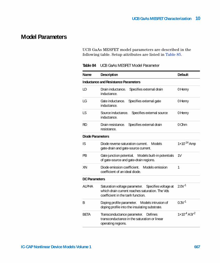
UCB GaAs MESFET Characterization 10
Model Parameters
IC-CAP Nonlinear Device Models Vo
UCB GaAs MESFET model parameters are described in the following table. Setup attributes are listed in Table 85.
Table 84 UCB GaAs MESFET Model Parameter
Name Description Default
Inductance and Resistance Parameters
LD Drain inductance. Specifies external drain inductance.
0 Henry
LG Gate inductance. Specifies external gate inductance.
0 Henry
LS Source inductance. Specifies external source inductance.
0 Henry
RD Drain resistance. Specifies external drain resistance.
0 Ohm
Diode Parameters
IS Diode reverse saturation current. Models gate-drain and gate-source current.
1×10-14 Amp
PB Gate junction potential. Models built-in potentials of gate-source and gate-drain regions.
1V
XN Diode emission coefficient. Models emission coefficient of an ideal diode.
1
DC Parameters
ALPHA Saturation voltage parameter. Specifies voltage at which drain current reaches saturation. The Vds coefficient in the tanh function.
2.0V-1
B Doping profile parameter. Models intrusion of doping profile into the insulating substrate.
0.3V-1
BETA Transconductance parameter. Defines transconductance in the saturation or linear operating regions.
1×10⁻⁴ A⋅V-2
lume 1 667
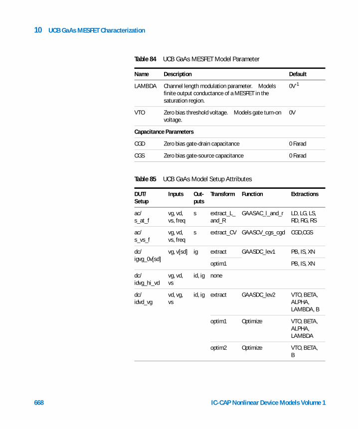
668
10 UCB GaAs MESFET Characterization
LAMBDA Channel length modulation parameter. Models finite output conductance of a MESFET in the saturation region.
0V-1
VTO Zero bias threshold voltage. Models gate turn-on voltage.
0V
Capacitance Parameters
CGD Zero bias gate-drain capacitance 0 Farad
CGS Zero bias gate-source capacitance 0 Farad
Table 85 UCB GaAs Model Setup Attributes
DUT/Setup
Inputs Out-puts
Transform Function Extractions
ac/s_at_f
vg, vd, vs, freq
s extract_L_and_R
GAASAC_l_and_r LD, LG, LS, RD, RG, RS
ac/s_vs_f
vg, vd, vs, freq
s extract_CV GAASCV_cgs_cgd CGD,CGS
dc/igvg_0v[sd]
vg, v[sd] ig extract GAASDC_lev1 PB, IS, XN
optim1 PB, IS, XN
dc/idvg_hi_vd
vg, vd, vs
id, ig none
dc/idvd_vg
vd, vg, vs
id, ig extract GAASDC_lev2 VTO, BETA, ALPHA, LAMBDA, B
optim1 Optimize VTO, BETA, ALPHA, LAMBDA
optim2 Optimize VTO, BETA, B
Table 84 UCB GaAs MESFET Model Parameter
Name Description Default
IC-CAP Nonlinear Device Models Volume 1
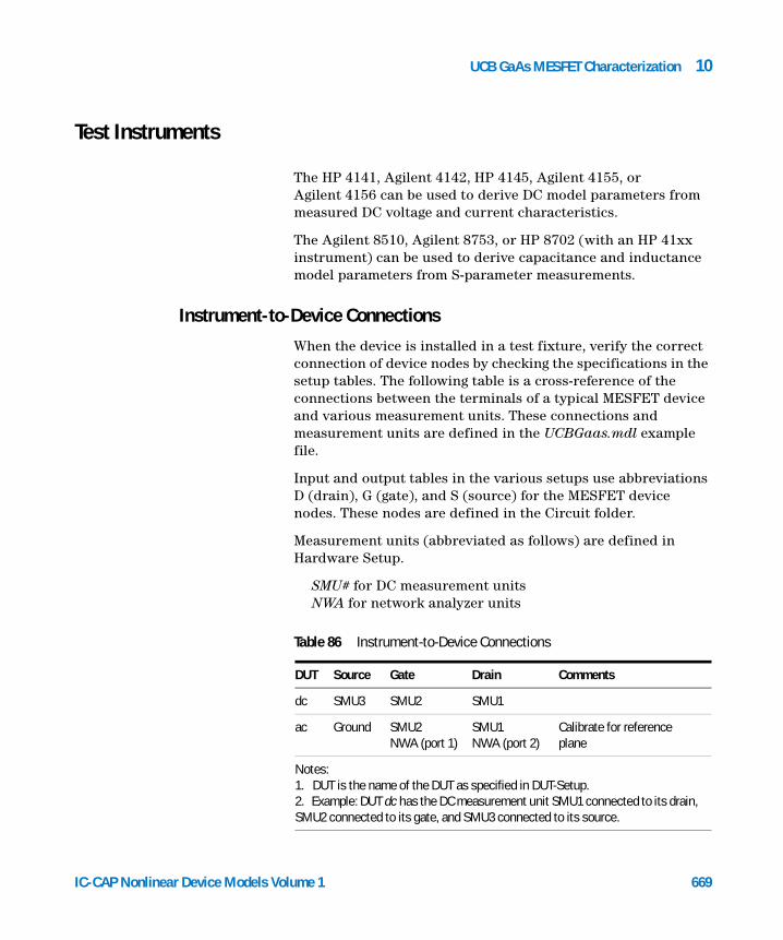
UCB GaAs MESFET Characterization 10
Test Instruments
IC-CAP Nonlinear Device Models Vo
The HP 4141, Agilent 4142, HP 4145, Agilent 4155, or Agilent 4156 can be used to derive DC model parameters from measured DC voltage and current characteristics.
The Agilent 8510, Agilent 8753, or HP 8702 (with an HP 41xx instrument) can be used to derive capacitance and inductance model parameters from S-parameter measurements.
Instrument-to-Device Connections
When the device is installed in a test fixture, verify the correct connection of device nodes by checking the specifications in the setup tables. The following table is a cross-reference of the connections between the terminals of a typical MESFET device and various measurement units. These connections and measurement units are defined in the UCBGaas.mdl example file.
Input and output tables in the various setups use abbreviations D (drain), G (gate), and S (source) for the MESFET device nodes. These nodes are defined in the Circuit folder.
Measurement units (abbreviated as follows) are defined in Hardware Setup.
SMU# for DC measurement unitsNWA for network analyzer units
Table 86 Instrument-to-Device Connections
DUT Source Gate Drain Comments
dc SMU3 SMU2 SMU1
ac Ground SMU2NWA (port 1)
SMU1NWA (port 2)
Calibrate for reference plane
Notes:1. DUT is the name of the DUT as specified in DUT-Setup.2. Example: DUT dc has the DC measurement unit SMU1 connected to its drain, SMU2 connected to its gate, and SMU3 connected to its source.
lume 1 669

10 UCB GaAs MESFET Characterization
Measuring and Extracting
670
This section provides general information as well as procedures for performing measurements and extractions of MESFET devices.
Measurement and Extraction Guidelines
The following guidelines are provided to help you achieve more successful model measurements and extractions.
Setting Instrument Options
Before starting a measurement, you can quickly verify instrument option settings. Save the current instrument option settings by saving the example file to <file_name>.mdl from the model window. Some of the Instrument Options specify instrument calibration. For the most accurate results, calibrate the instruments before taking IC-CAP measurements.
• DC measurements are generally taken with Integration Time = Medium.
• CV measurements in the femtofarad region usually require High Resolution = Yes and Measurement Freq (kHz) = 1000.
• When taking AC measurements with a network analyzer, several instrument settings are critical. In addition, the calibration must be performed on structures that have similar impedances as the stray parasitics of the DUT.
• Input power to the device is typically −10 to −30dBm (after port attenuation).
• Setting the averaging factor to the 2-to-4 range reduces measurement noise.
• Because IC-CAP requires the instrument to perform error correction, set Use Internal Calibration to Yes.
Experiment with the other network analyzer options to obtain the best results with specific devices.
IC-CAP Nonlinear Device Models Volume 1

UCB GaAs MESFET Characterization 10
IC-CAP Nonlinear Device Models Vo
Measuring Instruments
Ensure that the measuring instruments (specified by unit names in the input and output tables) are correctly connected to the DUT. Refer to Table 86 for a list of nodes and corresponding measurement units. The quality of the measuring equipment (instruments, cables, test fixture, transistor sockets, and probes) can influence the noise level in the measurements.
Ensure that all characteristics of the measurement stimulus and corresponding measured response are specified in the respective input and output tables.
Calibration
For some measurements the instruments or test hardware must be calibrated to remove non-device parasitics from the DUT. For MESFET devices, stray capacitance due to probe systems, bond pads, and so on should be calibrated out prior to each measurement.
For high-frequency 2-port measurements with a network analyzer, the reference plane of the instrument must be calibrated out to the DUT. IC-CAP relies on the internal calibration of the instruments for full error-corrected data. It is critical that calibration using OPEN, SHORT, THRU, and 50 ohm loads be properly done.
Extracting Model Parameters
For a given setup, you can find the extraction transforms in the Extract/Optimize folder. IC-CAP’s extraction algorithms exist as functions; choose Browse to list the functions available for a setup.
When the extract command is selected from the setup, all extractions in the setup are performed in the order listed in the setup. This order is usually critical to proper extraction performance. Extractions are typically completed instantly and the newly extracted model parameter values are placed in Model Parameters.
lume 1 671

672
10 UCB GaAs MESFET Characterization
IC-CAP provides setups for two extraction methods. In general, you only need to perform one of the methods in order to extract parameters.
Simulating Device Response
Simulation uses model parameter values currently in the Parameters table. A SPICE deck is created and the simulation performed. The output of the SPICE simulation is then read into IC-CAP as simulated data.
SPICE3 is the only simulator fully compatible with the IC-CAP UCBGaas.mdl configuration file is. You can also use the HPSPICE simulator if you modify the parameter names to match it. DC simulations generally run much faster than cv and AC simulations.
If simulated results are not as expected, use the simulation debugger (in the Tools menu) to examine the input and output simulation files. The output of manual simulations is not available for further processing by IC-CAP functions such as transforms and plots.
Displaying Plots
The Display Plot function displays all graphical plots defined in a setup. The currently active graphs are listed under the Plots folder in each setup. View the plots for agreement between measured and simulated data. Measured data is displayed as a solid line; simulated data is displayed as a dashed or dotted line.
Optimizing Model Parameters
Optimization of model parameters improves the agreement between measured and simulated data. An optimize transform whose Extract Flag is set to Yes is automatically called after any extraction that precedes it in the transform list.
Optimizing AC parameters can be very time consuming because of the number of SPICE simulations required.
IC-CAP Nonlinear Device Models Volume 1

UCB GaAs MESFET Characterization 10
Extraction Procedure Overview
IC-CAP Nonlinear Device Models Vo
This section describes the general procedure for extracting model parameter data from the UCB GaAs MESFET. The general procedure applies to all types of parameters. Differences between extracting one type and another are primarily in the types of instruments, test setups, and transforms used.
Parameters are extracted from measured or simulated data. Measured data is data taken directly from instruments connected to the DUT inputs and outputs. Simulated data are results from the simulator. Once measured and simulated data have been obtained, each data set can be plotted and compared in the Plot window.
The general extraction procedure is summarized next, starting with the measurement process.
1 Install the device to test in a test fixture and connect the test instruments.
2 Ensure the test fixture, signal source and measuring instruments, and workstation are physically and logically configured for the IC-CAP system.
3 Choose File > Open > Examples. Select UCBGaas.mdl and choose OK. Select Open to load the file and open the model window. Choose OK.
When the UCBGaas model window opens you are ready to begin measurement and extraction operations.
4 Enter the variable name EXTR_PAR at the Model level and enter NMF1 as its value. This allows the extractions to find the model parameters for the model name NMF1 within the subcircuit of the model file. This concept is covered in more detail in Chapter 12, “Circuit Modeling.”
5 Select the DUT and setup.
6 Issue the Measure command.
7 Issue the Extract command.
8 Issue the Simulate command.
9 Display the results.
lume 1 673
674
10 UCB GaAs MESFET Characterization
10 Fine tune the extracted parameters if needed by optimizing.
Parameter Measurement and Extraction
The recommended method for extracting UCB GaAs model parameters is presented next. In this extraction, external resistances are extracted from AC data.
NOTE If AC data is not available, an alternative method (described in “Alternate Extraction Method” on page 676) uses the Fukui technique [3] for extracting the resistances from DC data. Use the alternative method only if AC data is not available; the recommended method produces parameters that are more precise.
NOTE The UCB GaAs MESFET model extractions and Special Functions in IC-CAP only support the model as defined by the UCB SPICE3 implementation. There is a difference in several model parameter names from the Curtice model and the UCB model as they are implemented in the HPSPICE simulator. Valid model parameter names are listed in Table 84.
Parameter extractions are dependent on each other; to ensure accuracy extractions must be done in this order:
Inductances and resistances (AC) External inductance and resistance parameters are extracted from an S-parameter measurement at a single bias setting. The gate of the device is strongly forward-biased to make the device look like a short circuit. The setup s_at_f is used to take the measurements and extract the parameters LD, LG, LS, RD, RG, and RS.
Diode parameters (DC) Diode parameters PB, IS, and XN are extracted from data produced by the measurement of Ig versus Vg measured at zero drain voltage, with the source floating. The setup igvg_0vs or igvg_0vd is used to make the measurements and extractions, depending on whether the gate-source or gate-drain junction is preferred.
IC-CAP Nonlinear Device Models Volume 1

UCB GaAs MESFET Characterization 10
IC-CAP Nonlinear Device Models Vo
Other DC parameters (DC) The remaining DC parameters are extracted using two setups: idvd_vg and idvg_hi_vd. Use idvd_vg to measure Id versus Vg at different gate voltages, then use idvg_hi_vd to measure Id versus Vg at a constant drain voltage. Parameters VTO, BETA, ALPHA, LAMBDA, and B are then extracted from the resulting data.
AC (capacitance parameters) The capacitance parameters CGD and CGS are extracted from an S-parameter measurement using the setup s_vs_f. The measured data is first corrected using the inductances and resistances extracted in the initial step, then the capacitances are extracted from the corrected data.
Use a network analyzer to make the next set of measurements. S-parameter measurements are highly sensitive—the instrument must be properly calibrated.
1 Place the device to be measured in the test fixture.
NOTE For the ac/s_at_f and s_vs_f measurements, the SMUs connected to the network analyzer’s port bias connections must correspond to the SMUs in Table 86.2 Select the ac/s_at_f DUT/setup and choose Measure.
3 In the ac/s_at_f DUT/setup choose Extract to extract inductance and resistance parameters.
4 Select the ac/s_vs_f DUT/setup and choose Measure. Do not extract the parameters for this setup yet.
5 Disconnect the device from the network analyzer and directly connect it to the appropriate units for DC measurements.
6 Select the dc/ igvg_0vs or igvg_0vd DUT/setup and choose Measure.
7 Repeat Step 6, but choose Extract to extract diode parameters.
8 Repeat Step 6, but choose Optimize.
9 Select the dc/idvg_hi_vd DUT/setup and choose Measure to measure Id versus Vg at a constant Vd.
lume 1 675
676
10 UCB GaAs MESFET Characterization
10 Select the dc/idvd_vg DUT/setup and perform the measure and extract steps to measure and extract the other DC parameters.
11 Repeat Step 10, but choose Optimize.
12 Select the ac/s_vs_f DUT/setup and choose Extract to extract the capacitances from the data that was measured in step 4.
All model parameters are extracted and their values added to the Parameters table; they can be viewed in the Model Parameters folder.
Alternate Extraction Method
If AC data is not available, IC-CAP supports an alternate method for extracting UCB MESFET model parameters. This procedure uses the Fukui technique [3]; external resistances are extracted along with the diode parameters from DC data—this differs from the recommended method. Use this method only if the AC data is not available—this alternate method produces parameters that are less precise than those of the recommended method.
Parameter extractions are dependent on each other; to ensure accuracy extractions must be done in the following order.
Resistance and diode parameters (DC) Using DC measurements only, this procedure uses the Fukui algorithm to extract the resistance parameters RD, RG, and RS from DC data (refer to Table 84). Diode parameters PB, IS, and XN are also extracted. The extraction requires the setups listed in the following table.
Table 87 Resistance and Diode Measurement and Extraction Setups for the Alternative Method
idvg_low_vd
Id versus Vg
Small Vd
igvg_0vs Ig versus Vg Vs=0, with Drain floating
igvg_0vd Ig versus Vg Vd=0, with Source floating
IC-CAP Nonlinear Device Models Volume 1
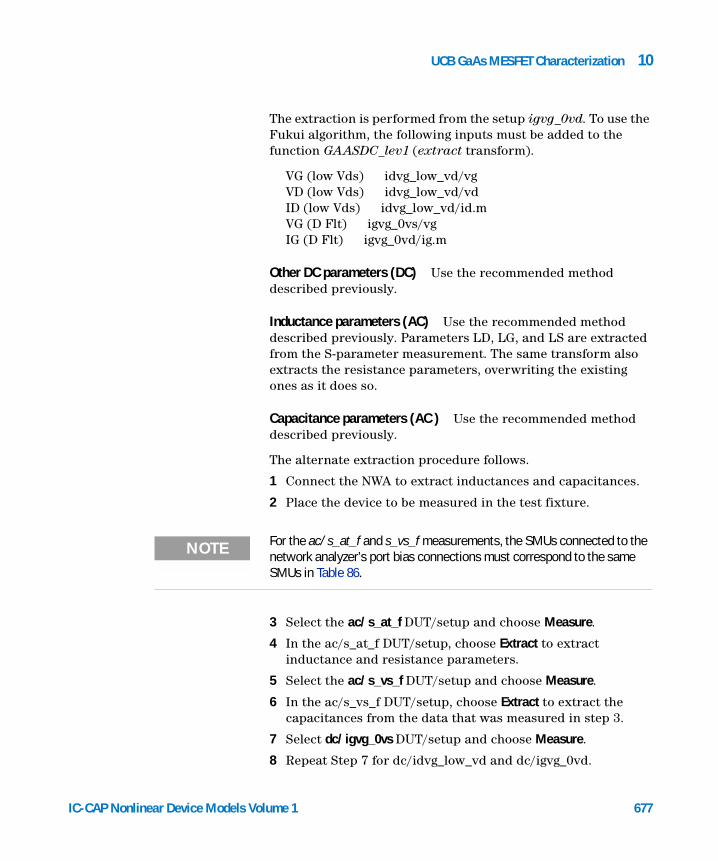
UCB GaAs MESFET Characterization 10
IC-CAP Nonlinear Device Models Vo
The extraction is performed from the setup igvg_0vd. To use the Fukui algorithm, the following inputs must be added to the function GAASDC_lev1 (extract transform).
VG (low Vds) idvg_low_vd/vgVD (low Vds) idvg_low_vd/vdID (low Vds) idvg_low_vd/id.mVG (D Flt) igvg_0vs/vgIG (D Flt) igvg_0vd/ig.m
Other DC parameters (DC) Use the recommended method described previously.
Inductance parameters (AC) Use the recommended method described previously. Parameters LD, LG, and LS are extracted from the S-parameter measurement. The same transform also extracts the resistance parameters, overwriting the existing ones as it does so.
Capacitance parameters (AC ) Use the recommended method described previously.
The alternate extraction procedure follows.
1 Connect the NWA to extract inductances and capacitances.
2 Place the device to be measured in the test fixture.
NOTE For the ac/s_at_f and s_vs_f measurements, the SMUs connected to the network analyzer’s port bias connections must correspond to the same SMUs in Table 86.
3 Select the ac/s_at_f DUT/setup and choose Measure.
4 In the ac/s_at_f DUT/setup, choose Extract to extract inductance and resistance parameters.
5 Select the ac/s_vs_f DUT/setup and choose Measure.
6 In the ac/s_vs_f DUT/setup, choose Extract to extract the capacitances from the data that was measured in step 3.
7 Select dc/igvg_0vs DUT/setup and choose Measure.
8 Repeat Step 7 for dc/idvg_low_vd and dc/igvg_0vd.
lume 1 677
678
10 UCB GaAs MESFET Characterization
9 In the dc/igvg_0vd DUT/setup, choose Extract to extract the resistance and diode parameters from the measured data for the three DC setups.
10 Repeat Step 9 but choose Optimize.
11 Select the dc/idvg_hi_vd DUT/setup and choose Measure to measure Id versus Vg at a constant Vd.
12 In the dc/idvd_vg DUT/setup, repeat the Measure and Extract steps to measure and extract the other DC parameters.
13 Repeat step 13 but choose Optimize.
Simulating
To simulate any individual setup, choose Simulate with that setup active. Simulations can be performed in any order once all of the model parameters have been extracted.
For more information on simulation, refer to Chapter 6, “Simulating,” in the IC-CAP User’s Guide.
Displaying Plots
To display plots issue the Display Plot command from a DUT to display the plots for all setups in that DUT. The Plots use the most recent set of measured and simulated data. Viewing plots is an ideal way to compare measured and simulated data to determine if further optimization would be useful. For more information on Plots, refer to Chapter 10, “Printing and Plotting,” in the IC-CAP User’s Guide.
Optimizing
The optimization operation uses a numerical approach to minimize errors between measured and simulated data. As with the other IC-CAP commands, optimization can be performed at either the DUT or setup level. Optimization is more commonly performed from setups—optimization for all setups under a DUT is rarely required.
IC-CAP Nonlinear Device Models Volume 1
UCB GaAs MESFET Characterization 10
IC-CAP Nonlinear Device Models Vo
Optimization is typically interactive in nature, with the best results obtained when you specify the characteristics of the desired results.
For more information on optimization, refer to Chapter 7, “Optimizing,” in the IC-CAP User’s Guide.
lume 1 679
10 UCB GaAs MESFET Characterization
Extraction Algorithms
680
This section describes the extraction algorithms used for inductance, capacitance, DC, and series resistance parameters of the UCB GaAs MESFET.
Inductance and Resistance Extraction
Inductors and resistors that are in series with each terminal of the MESFET are measured with a network analyzer at a high frequency and with the gate strongly forward-biased. Under these conditions the AC model for each terminal is reduced to a series R-L circuit. Inductors LD, LG, and LS and resistors RD, RG, and RS are extracted simultaneously from the measured impedance at the gate and drain ports.
DC Parameter Extractions
DC extractions are separated between the diode and forward active controlling parameters. Diode parameters PB, IS, and XN are extracted using a method similar to the method used for a silicon diode. The diode is swept over a forward bias and linear least-squares curve fits will produce the built-in potential and forward conduction properties.
The forward active region is extracted from measurements of the MESFET in both the linear and saturated modes of operation. The difference between the equations defining these two regions is a tanh(ALPHA ⋅ Vds) multiplier in the linear mode. The threshold can be obtained from a least-squares fit to the linear region. These equations are solved to produce ALPHA, B, BETA, LAMDA, and VTO.
Capacitance Parameter Extractions
The capacitance of the gate-to-drain (CGD) and gate-to-source (CGS) is measured with S-parameters over typical operating frequencies. Because the inductances and series resistance are already known, these capacitances can be extracted from the corrected impedances measured at the gate and drain ports.
IC-CAP Nonlinear Device Models Volume 1
UCB GaAs MESFET Characterization 10
References
IC-CAP Nonlinear Device Models Vo
1 Hermann Statz, Paul Newman, Irl W. Smith, Robert A. Pucel, & Hermann A. Haus. GaAs FET Device and Circuit Simulation in SPICE, IEEE Transactions on Electron Devices, Vol. ED-34, No. 2, February 1987.
2 Tom Quarles et al. SPICE Version 3A7 User’s Guide, University of California, Berkeley.
3 H. Fukui, Determination of the Basic Device Parameters of a GaAs MESFET, The Bell System Technical Journal, Vol. 58, No. 3, March 1979.
lume 1 681

682
10 UCB GaAs MESFET Characterization
IC-CAP Nonlinear Device Models Volume 1
Agilent 85190A IC-CAP 2008Nonlinear Device Models Volume 1
11Curtice GaAs MESFET Characterization
Curtice GaAs MESFET Model 685
Simulators 686
Model Parameters 688
Test Instruments 692
Measuring and Extracting 694
Extraction Algorithms 704
References 705
This chapter describes the Curtice GaAs MESFET transistor supported by HPSPICE. Descriptions of model setup, instrument connections, and model parameters are included as well as test instrument information. Procedures for extracting AC and DC model parameters from GaAs MESFET transistors using the Curtice GaAs MESFET model are also included. These model parameters describe the operating characteristics of the device under test (DUT), and can be derived from either simulated or direct measurements of the DUT.
The IC-CAP Curtice GaAs modeling module provides setups that can be used for general measurement and model extraction for GaAs technology. Two example files are provided for the Curtice GaAs MESFET transistor:
CGaas1.mdl extracts parameters for the quadratic model
CGaas2.mdl extracts parameters for the cubic model
The IC-CAP system offers the flexibility to modify any measurement or simulation specification.
683Agilent Technologies

684
11 Curtice GaAs MESFET Characterization
The model extractions provided are also intended for general GaAs IC processes. If you have another method of extracting specific model parameters, you can do so with the Program function or by writing a function in C and linking it to the function list. Details on the Program transform and writing user-defined C language routines are explained in Chapter 9, “Using Transforms and Functions,” in the IC-CAP User’s Guide.
IC-CAP Nonlinear Device Models Volume 1
Curtice GaAs MESFET Characterization 11
Curtice GaAs MESFET Model
IC-CAP Nonlinear Device Models Vo
The Curtice GaAs MESFET model is contained in the IC-CAP example files CGaas1.mdl and CGaas2.mdl. These files consist of two levels of models that are based on a model developed at RCA and implemented in many SPICE versions. In level 1 (quadratic) model (CGaas1.mdl), drain current is proportional to the square of the gate to source voltage multiplied by the hyperbolic tangent of the drain to source voltage [1]. Level 2 (Cubic) model (CGaas2.mdl), relates the drain current to the third-order polynomial of the gate and drain voltages times the hyperbolic tangent of the drain voltage [2].
The IC-CAP implementation of the model also includes voltage-dependent capacitances, gate-to-source and gate-to-drain junction diodes, and the series resistances and inductances at the gate, source, and drain.
lume 1 685
11 Curtice GaAs MESFET Characterization
Simulators
686
This model is supported only by the HPSPICE simulator in IC-CAP.
NOTE Simulators are provided as a courtesy to IC-CAP users; they are not supported by Agilent Technologies.
The default nominal temperature for SPICE3 is 25°C. To force another nominal temperature, set the TNOM variable to the desired value.
The HPSPICE syntax for the Curtice GaAs MESFET element statement is:
JXXXXXXX ND NG NS MNAME
where:
An example of the Curtice GaAs MESFET device model call is: J2 1 2 3 CMES
The HPSPICE syntax for the .MODEL definition is
.MODEL MNAME RCAY TYPE PNAME1=PVAL1 PNAME2=PVAL2 ...
where:
JXXXXXXX indicates Curtice MESFET device name (any name that begins with J)
ND indicates drain node number
NG indicates gate node number
NS indicates source node number
MNAME indicates model name
MNAME indicates model name
IC-CAP Nonlinear Device Models Volume 1

Curtice GaAs MESFET Characterization 11
IC-CAP Nonlinear Device Models Vo
The parameter MODEL in the .MODEL description must be set:
MODEL = 1 indicates Curtice level 1 quadratic model
MODEL = 2 indicates Curtice level 2 cubic model
RCAY key word specifying a GaAs MESFET model
TYPE indicates NJF (N-channel MESFET) or PJF (P-channel MESFET)
PNAME# indicates Curtice GaAs MESFET parameter name
PVAL# indicates parameter value of PNAME#
lume 1 687

11 Curtice GaAs MESFET Characterization
Model Parameters
688
Curtice GaAs MESFET model parameters are summarized in the following table. Table 89 lists the parameters with descriptions and default values. Setup attributes are listed in Table 90.
Table 88 Summary of Curtice GaAs MESFET Model Parameters
Parameter Type Controlling Model Parameters
Inductance and Resistance LD, LG, LS, RD, RG, RS
Diode IS, VBI, N
Threshold Level 1: VTOLevel 2: A0, A1, A2, A3
Linear and Saturation Level 1: BETA, LAMBDA, ALPHALevel 2: BETA, GAMMA
Capacitance and AC CGDO, CGSO, CDS, RDSO, RIN, A5optionally: CGD, CGS, TAU
Table 89 Curtice GaAs MESFET Model Parameters
Name Description Default
Inductance and Resistance Parameters
LD Drain Inductance. Specifies external drain inductance.
0 Henry
LG Gate Inductance. Specifies external gate inductance. 0 Henry
LS Source Inductance. Specifies external source inductance.
0 Henry
RD Drain Resistance. Specifies external drain resistance. 0 Ohm
RG Gate Resistance. Specifies external gate resistance. 0 Ohm
RS Source Resistance. Specifies external source resistance.
0 Ohm
IC-CAP Nonlinear Device Models Volume 1
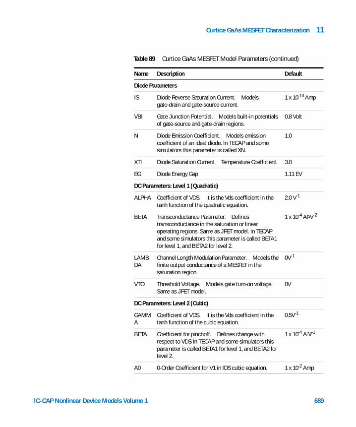
Curtice GaAs MESFET Characterization 11
IC-CAP Nonlinear Device Models Vo
Diode Parameters
IS Diode Reverse Saturation Current. Models gate-drain and gate-source current.
1 x 10-14 Amp
VBI Gate Junction Potential. Models built-in potentials of gate-source and gate-drain regions.
0.8 Volt
N Diode Emission Coefficient. Models emission coefficient of an ideal diode. In TECAP and some simulators this parameter is called XN.
1.0
XTI Diode Saturation Current. Temperature Coefficient. 3.0
EG Diode Energy Gap 1.11 EV
DC Parameters: Level 1 (Quadratic)
ALPHA Coefficient of VDS. It is the Vds coefficient in the tanh function of the quadratic equation.
2.0 V-1
BETA Transconductance Parameter. Defines transconductance in the saturation or linear operating regions. Same as JFET model. In TECAP and some simulators this parameter is called BETA1 for level 1, and BETA2 for level 2.
1 x 10⁻⁴ AÞV-2
LAMBDA
Channel Length Modulation Parameter. Models the finite output conductance of a MESFET in the saturation region.
0V-1
VTO Threshold Voltage. Models gate turn-on voltage. Same as JFET model.
0V
DC Parameters: Level 2 (Cubic)
GAMMA
Coefficient of VDS. It is the Vds coefficient in the tanh function of the cubic equation.
0.5V-1
BETA Coefficient for pinchoff. Defines change with respect to VDS In TECAP and some simulators this parameter is called BETA1 for level 1, and BETA2 for level 2.
1 x 10⁻⁴ A⋅V-1
A0 0-Order Coefficient for V1 in IDS cubic equation. 1 x 10⁻² Amp
Table 89 Curtice GaAs MESFET Model Parameters (continued)
Name Description Default
lume 1 689
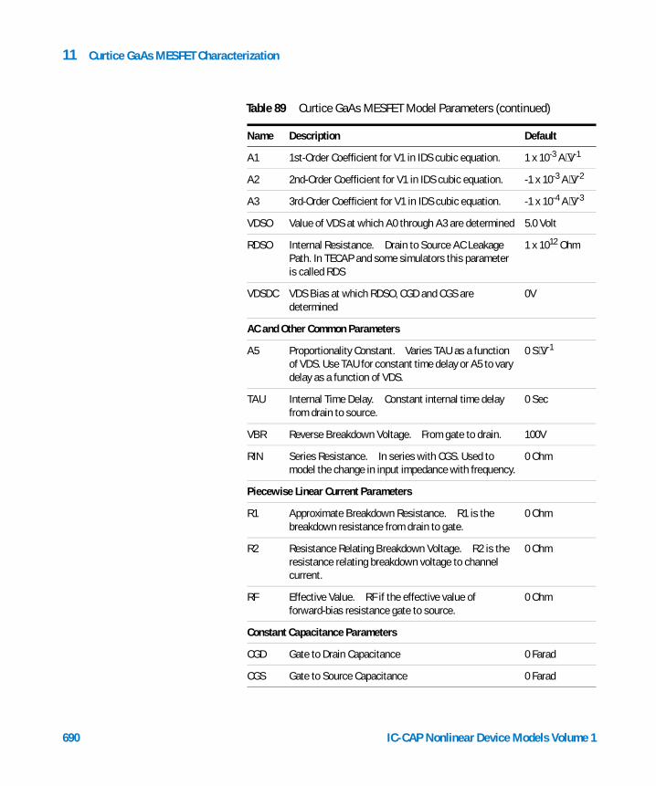
690
11 Curtice GaAs MESFET Characterization
A1 1st-Order Coefficient for V1 in IDS cubic equation. 1 x 10⁻³ A⋅V-1
A2 2nd-Order Coefficient for V1 in IDS cubic equation. -1 x 10⁻³ A⋅V-2
A3 3rd-Order Coefficient for V1 in IDS cubic equation. -1 x 10⁻⁴ A⋅V-3
VDSO Value of VDS at which A0 through A3 are determined 5.0 Volt
RDSO Internal Resistance. Drain to Source AC Leakage Path. In TECAP and some simulators this parameter is called RDS
1 x 10¹² Ohm
VDSDC VDS Bias at which RDSO, CGD and CGS are determined
0V
AC and Other Common Parameters
A5 Proportionality Constant. Varies TAU as a function of VDS. Use TAU for constant time delay or A5 to vary delay as a function of VDS.
0 S⋅V-1
TAU Internal Time Delay. Constant internal time delay from drain to source.
0 Sec
VBR Reverse Breakdown Voltage. From gate to drain. 100V
RIN Series Resistance. In series with CGS. Used to model the change in input impedance with frequency.
0 Ohm
Piecewise Linear Current Parameters
R1 Approximate Breakdown Resistance. R1 is the breakdown resistance from drain to gate.
0 Ohm
R2 Resistance Relating Breakdown Voltage. R2 is the resistance relating breakdown voltage to channel current.
0 Ohm
RF Effective Value. RF if the effective value of forward-bias resistance gate to source.
0 Ohm
Constant Capacitance Parameters
CGD Gate to Drain Capacitance 0 Farad
CGS Gate to Source Capacitance 0 Farad
Table 89 Curtice GaAs MESFET Model Parameters (continued)
Name Description Default
IC-CAP Nonlinear Device Models Volume 1
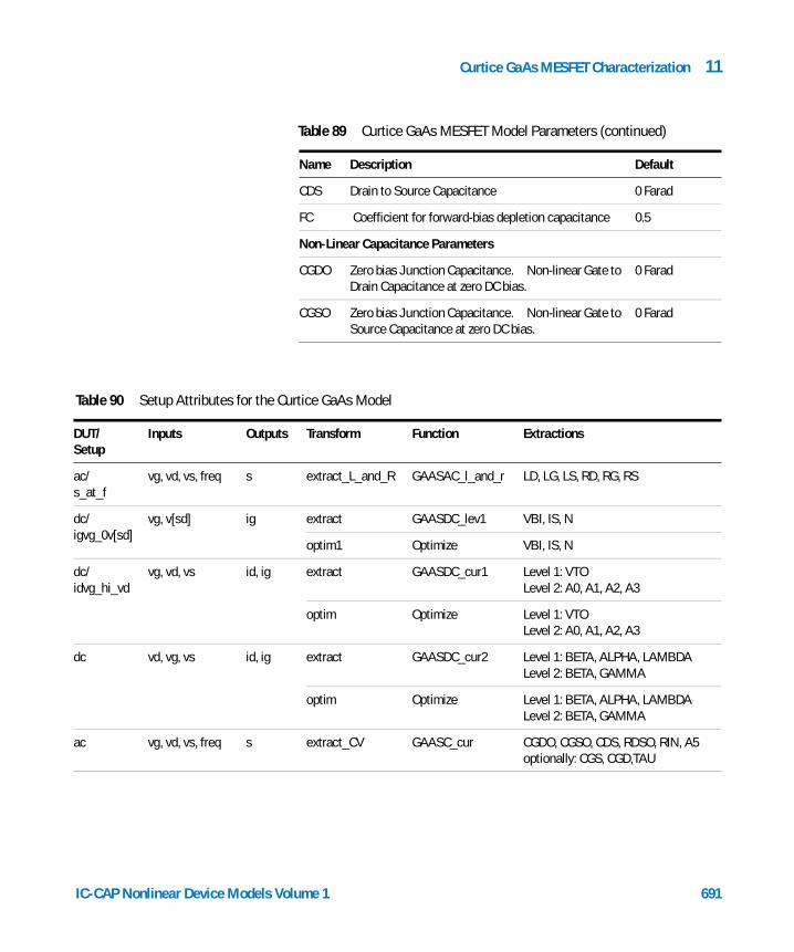
Curtice GaAs MESFET Characterization 11
IC-CAP Nonlinear Device Models Vo
CDS Drain to Source Capacitance 0 Farad
FC Coefficient for forward-bias depletion capacitance 0.5
Non-Linear Capacitance Parameters
CGDO Zero bias Junction Capacitance. Non-linear Gate to Drain Capacitance at zero DC bias.
0 Farad
CGSO Zero bias Junction Capacitance. Non-linear Gate to Source Capacitance at zero DC bias.
0 Farad
Table 89 Curtice GaAs MESFET Model Parameters (continued)
Name Description Default
Table 90 Setup Attributes for the Curtice GaAs Model
DUT/Setup
Inputs Outputs Transform Function Extractions
ac/s_at_f
vg, vd, vs, freq s extract_L_and_R GAASAC_l_and_r LD, LG, LS, RD, RG, RS
dc/igvg_0v[sd]
vg, v[sd] ig extract GAASDC_lev1 VBI, IS, N
optim1 Optimize VBI, IS, N
dc/idvg_hi_vd
vg, vd, vs id, ig extract GAASDC_cur1 Level 1: VTOLevel 2: A0, A1, A2, A3
optim Optimize Level 1: VTOLevel 2: A0, A1, A2, A3
dc vd, vg, vs id, ig extract GAASDC_cur2 Level 1: BETA, ALPHA, LAMBDALevel 2: BETA, GAMMA
optim Optimize Level 1: BETA, ALPHA, LAMBDALevel 2: BETA, GAMMA
ac vg, vd, vs, freq s extract_CV GAASC_cur CGDO, CGSO, CDS, RDSO, RIN, A5optionally: CGS, CGD,TAU
lume 1 691
11 Curtice GaAs MESFET Characterization
Test Instruments
692
The HP 4141, Agilent 4142, or HP 4145 can be used to derive DC model parameters from measured DC voltage and current characteristics.
The Agilent 8510, Agilent 8753, or HP 8702 (with an HP 41xx instrument) can be used to derive capacitance and inductance model parameters from S-parameter measurements.
Instrument-to-Device Connections
When the device is installed in a test fixture, verify the identity of device nodes by checking the inputs and outputs for the appropriate DUTs. The following table is a cross reference of the connections between the terminals of a typical MESFET device and various measurement units. These connections and measurement units are defined in CGaas1.mdl and CGaas2.mdl example files.
Input and output tables in the various setups use abbreviations D (drain), G (gate), and S (source) for the MESFET device nodes. These nodes are defined in the Circuit folder.
Measurement units (abbreviated as follows) are defined in Hardware Setup.
SMU# for DC measurement unitsNWA for network analyzer units
IC-CAP Nonlinear Device Models Volume 1
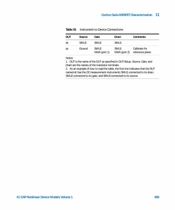
Curtice GaAs MESFET Characterization 11
IC-CAP Nonlinear Device Models Vo
Table 91 Instrument-to-Device Connections
DUT Source Gate Drain Comments
dc SMU3 SMU2 SMU1
ac Ground SMU2NWA (port 1)
SMU1NWA (port 2)
Calibrate forreference plane
Notes:1. DUT is the name of the DUT as specified in DUT-Setup. Source, Gate, and Drain are the names of the transistor terminals. 2. As an example of how to read the table, the first line indicates that the DUT named dc has the DC measurement instruments SMU1 connected to its drain, SMU2 connected to its gate, and SMU3 connected to its source.
lume 1 693

11 Curtice GaAs MESFET Characterization
Measuring and Extracting
694
This section general information as well as procedures for performing measurements and extractions of MESFET devices.
Measurement and Extraction Guidelines
The following guidelines are provided to help you achieve more successful model measurements and extractions.
Setting Instrument Options
Before starting a measurement, you can quickly verify instrument options settings. Save the current instrument option settings by saving the model file to <file_name>.mdl from the model window. Some of the Instrument Options specify instrument calibration. For the most accurate results, calibrate the instruments before taking IC-CAP measurements.
• DC measurements are generally taken with Integration Time = Medium.
• CV measurements in the femtofarad region usually require High Resolution = Yes and Measurement Freq (kHz) = 1000.
• When taking AC measurements with a network analyzer, several instrument settings are critical. In addition, the calibration must be performed on structures that have similar impedances as the stray parasitics of the DUT.
• Input power to the device is typically −10 to −30dBm (after port attenuation).
• Setting the averaging factor to the 2-to-4 range reduces measurement noise.
• Because IC-CAP requires the instrument to perform error correction, set Use Internal Calibration to Yes.
Experiment with the other network analyzer options to obtain the best results with specific devices.
IC-CAP Nonlinear Device Models Volume 1
Curtice GaAs MESFET Characterization 11
IC-CAP Nonlinear Device Models Vo
Measuring Instruments
Ensure that the measuring instruments (specified by unit names in the input and output tables) are correctly connected to the DUT. Refer to Table 91 for a list of nodes and corresponding measurement units. The quality of the measuring equipment (instruments, cables, test fixture, transistor sockets, and probes) can influence the noise level in the measurements.
Ensure that all characteristics of the measurement stimulus and corresponding measured response are specified in the respective input and output tables.
Calibration
For some measurements the instruments or test hardware must be calibrated to remove non-device parasitics from the DUT. For MESFET devices, stray capacitance due to probe systems, bond pads, and so on should be calibrated out prior to each measurement.
For high-frequency 2-port measurements with a network analyzer, the reference plane of the instrument must be calibrated out to the DUT. IC-CAP relies on the internal calibration of the instruments for full error-corrected data. It is critical that calibration using OPEN, SHORT, THRU, and 50 ohm loads be properly done.
Extracting Model Parameters
IC-CAP’s extraction algorithms exist as transforms in the function list, under Extractions. Extraction transforms for a given setup are listed in the transform tile for the setup.
When the extract command is issued from the setup level, all extractions in the setup are performed in the order listed in the setup; this order is usually critical to proper extraction performance. The extractions are typically completed instantly and the newly extracted parameter values are placed in Model Parameters.
The configuration file supplied with IC-CAP contains the setups for two different extraction methods, and two different sets of model parameters (level 1 and 2). In general only one set of
lume 1 695
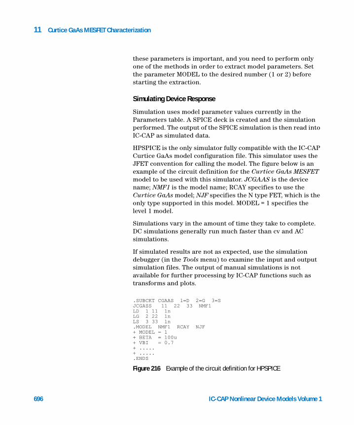
696
11 Curtice GaAs MESFET Characterization
these parameters is important, and you need to perform only one of the methods in order to extract model parameters. Set the parameter MODEL to the desired number (1 or 2) before starting the extraction.
Simulating Device Response
Simulation uses model parameter values currently in the Parameters table. A SPICE deck is created and the simulation performed. The output of the SPICE simulation is then read into IC-CAP as simulated data.
HPSPICE is the only simulator fully compatible with the IC-CAP Curtice GaAs model configuration file. This simulator uses the JFET convention for calling the model. The figure below is an example of the circuit definition for the Curtice GaAs MESFET model to be used with this simulator. JCGAAS is the device name; NMF1 is the model name; RCAY specifies to use the Curtice GaAs model; NJF specifies the N type FET, which is the only type supported in this model. MODEL = 1 specifies the level 1 model.
Simulations vary in the amount of time they take to complete. DC simulations generally run much faster than cv and AC simulations.
If simulated results are not as expected, use the simulation debugger (in the Tools menu) to examine the input and output simulation files. The output of manual simulations is not available for further processing by IC-CAP functions such as transforms and plots.
.SUBCKT CGAAS 1=D 2=G 3=SJCGASS 11 22 33 NMF1LD 1 11 1nLG 2 22 1nLS 3 33 1n.MODEL NMF1 RCAY NJF+ MODEL = 1+ BETA = 100u+ VBI = 0.7+ .....+ ......ENDS
Figure 216 Example of the circuit definition for HPSPICE
IC-CAP Nonlinear Device Models Volume 1
Curtice GaAs MESFET Characterization 11
IC-CAP Nonlinear Device Models Vo
Displaying Plots
The Display Plot function displays all graphical plots defined in a setup. The currently active graphs are listed under the Plots folder in each setup. View the plots for agreement between measured and simulated data. Measured data is displayed as a solid line; simulated data is displayed as a dashed or dotted line.
Optimizing Model Parameters
Optimization of model parameters improves the agreement between measured and simulated data. An optimize transform whose Extract Flag is set to Yes is automatically called after any extraction that precedes it in the transform list.
Optimizing AC parameters can be very time consuming because of the number of SPICE simulations required.
Extraction Procedure Overview
This section describes the general procedure for extracting model parameter data from the Curtice GaAs MESFET. The procedure applies to all types of parameters. The differences between extracting one type and another lie primarily in the types of instruments, setups, and transforms used.Parameters can be extracted from measured or simulated data. Measured data is data taken directly from instruments connected to the DUT inputs and outputs. Simulated data are results from the simulator. Once measured and simulated data have been obtained, both data sets can be plotted and compared.
The general extraction procedure is summarized next, starting with the measurement process.
1 Install the device to test in a test fixture and connect the test instruments.
2 Ensure the test fixture, signal source and measuring instruments, and workstation are physically and logically configured for the IC-CAP system.
lume 1 697
698
11 Curtice GaAs MESFET Characterization
3 Choose File > Open > Examples. Select CGaas2.mdl and choose OK. Select Open to load the file and open the model window. Choose OK.
When the CGaas2 model window opens you are ready to begin measurement and extraction operations.
4 Enter the variable name EXTR_PAR at the model level and enter NMF1 as its value. This allows the extractions to find the model parameters for the model name NMF1 within the subcircuit of the model file. This concept is covered in more detail in Chapter 12, “Circuit Modeling”.
5 Select the DUT and Setup.
6 Execute the Measure command.
7 Execute the Extract command.
8 Execute the Simulate command.
9 Display the results.
10 Fine tune the extracted parameters if needed by optimizing.
Parameter Measurement and Extraction
The recommended method for extracting Curtice GaAs model parameters is presented next. In this extraction, external resistances are extracted from AC data.
NOTE If AC data is not available, an alternative method (described in the section “Alternate Extraction Method” on page 701) uses the Fukui technique [3] for extracting the resistances from DC data. Use the alternative method only if AC data is not available; the recommended method produces parameters that are more precise.
The Curtice GaAs MESFET model is a 2-level model. IC-CAP supports and extracts parameters for both levels of this model. The following procedure extracts parameters for level 1 or 2 depending on the value of the parameter MODEL.
Parameter extractions are dependent on each other; to ensure accuracy extractions must be done in this order:
IC-CAP Nonlinear Device Models Volume 1
Curtice GaAs MESFET Characterization 11
IC-CAP Nonlinear Device Models Vo
Inductance and resistance parameters (AC) External inductance and resistance parameters are extracted from an S-parameter measurement at a single bias setting. The gate of the device is strongly forward biased to make the device look like a short circuit. The s_at_f setup is used to take the measurements and extract the parameters LD, LG, LS, RD, RG, and RS.
Diode parameters (DC) Diode parameters VBI, IS, and N are extracted from data produced by the measurement of Id versus Vg measured at zero drain voltage, with the source floating. The igvg_0vs or igvg_0vd setup is used to make the measurements and extractions, depending on whether the gate-source or gate-drain junction is preferred.
Threshold parameters (DC) Parameters that describe the threshold characteristics are extracted using Id versus Vg measurement at a high drain voltage. The idvg_hi_vd setup is used for this extraction. For the level 1 model, VTO will be extracted; for the level 2 model, A0, A1, A2 and A3 will be extracted.
Linear and saturation parameters (DC) Parameters that control the linear and saturation regions of device operation are extracted using Id versus Vd measurement at different gate voltages. The idvd_vg setup is used for this extraction. BETA, LAMBDA and ALPHA are extracted for the level 1 model; BETA and GAMMA are extracted for the level 2 model.
Capacitance parameters (AC) Capacitance parameters CGDO and CGSO, and AC parameters A5, CDS, RDSO and RIN are extracted from an S-parameter measurement using the s_vs_f setup. Measured data is corrected using the inductances and resistances extracted in the initial step; capacitance and other AC parameters are then extracted from corrected data.
By defining IC-CAP system variables LINEAR_CGS, LINEAR_CGD, and CONSTANT_TAU and setting their values to true, CGS, CGD, and TAU, respectively, can be extracted.
lume 1 699
700
11 Curtice GaAs MESFET Characterization
Use a network analyzer to make the next set of measurements. S-parameter measurements are highly sensitive—it is important that the instrument be properly calibrated.
1 Place the device to be measured in the test fixture.
NOTE For the ac/s_at_f and s_vs_f measurements, the SMUs connected to the network analyzer’s port bias connections must correspond to the SMUs in Table 91.
2 Select the ac/s_at_f DUT/Setup and choose Measure.
3 In the ac/s_at_f DUT/Setup select Extract to extract the inductance and resistance parameters.
4 Select the ac/s_vs_f DUT/Setup and choose Measure. Do not extract the parameters for this setup yet.
5 Disconnect the device from the network analyzer and directly connect it to the appropriate units for DC measurements.
6 Select the dc/ igvg_0vs or igvg_0vd DUT/Setup and choose Measure.
7 Repeat Step 6, but choose Extract to extract the diode parameters.
8 Repeat Step 6, but choose Optimize.
9 Select the dc/idvg_hi_vd DUT/Setup and choose Measure to measure Id versus Vg at a constant Vd.
10 Select the dc/idvd_vg DUT/Setup and repeat the Measure and Extract steps to measure and extract the other DC parameters.
11 Repeat Step 10, but choose Optimize.
12 Select the ac/s_vs_f DUT/Setup and choose Extract to extract the capacitances from the data that was measured in step 4.
All model parameters are extracted and their values added to the Parameters table; they can be viewed in the Model Parameters folder.
IC-CAP Nonlinear Device Models Volume 1
Curtice GaAs MESFET Characterization 11
Alternate Extraction Method
IC-CAP Nonlinear Device Models Vo
If AC data is not available, IC-CAP supports an alternate method for extracting Curtice MESFET model parameters. This procedure uses the Fukui technique [3]; external resistances are extracted along with the diode parameters from DC data—this differs from the recommended method. Use this method only if the AC data is not available—this alternate method produces parameters that are less precise than those of the recommended method.
Resistance and diode parameters (DC) Using DC measurements only, this procedure uses the Fukui algorithm to extract resistance parameters RD, RG, and RS from DC data. Diode parameters VBI, IS, and N are also extracted. The extraction requires the setups listed in the following table.
This extraction is located in the igvg_0vd setup. To use the Fukui algorithm, add the following inputs to the function GAASDC_lev1.
VG (low Vds) idvg_low_vd/vgVD (low Vds) idvg_low_vd/vdID (low Vds) idvg_low_vd/id.mVG (D Flt) igvg_0vs/vgIG (D Flt) igvg_0vs/ig.m
Threshold Parameters ( ) Use the recommended method for measuring and extracting threshold parameters.
Linear & Saturation Parameters ( ) Use the recommended method for measuring and extracting linear & saturation parameters.
Table 92 Resistance and Diode Measurement and Extraction Setups
igvg_0vd Ig versus Vg Vd=0, with Source floating
idvg_low_vd Id versus Vg Small Vd
gvg_0vs Ig versus Vg Vs=0, with Drain floating
lume 1 701
702
11 Curtice GaAs MESFET Characterization
Inductance Parameters (AC) Use the recommended method for measuring and extracting inductances. The parameters LD, LG, and LS are extracted from the S-parameter measurement. In addition, the Transform also extracts and overwrites the resistance parameters.
Capacitance Parameters ( ) Use the recommended method for measuring and extracting capacitance parameters.
The alternate extraction procedure follows.
1 Connect the NWA to extract inductances and capacitances.
2 Place the device to be measured in the test fixture.
NOTE For the ac/s_at_f and s_vs_f measurements, the SMUs connected to the network analyzer’s port bias connections must correspond to the same SMUs in Table 91.
3 Select the ac/s_at_f DUT/Setup and choose Measure.
4 Repeat Step 2, but select Extract to extract the inductance and resistance parameters
5 Select the ac/s_vs_f DUT/Setup and choose Measure. Do not extract the parameters for this setup yet.
6 Select the ac/s_vs_f DUT/Setup and choose Extract to extract the capacitances from the data that was measured in step 3.
7 Select dc/igvg_0vs DUT/Setup and choose Measure.
8 Repeat Step 8 for dc/idvg_low_vd and dc/igvg_0vd.
9 In the dc/igvg_0vd DUT/Setup, choose Extract to extract the resistance and diode parameters from the measured data for the three DC Setups.
10 Repeat Step 9 but choose Optimize.
11 Select the dc/idvg_hi_vd DUT/Setup and choose Measure to measure Id versus Vg at a constant Vd.
12 Select the dc/idvd_vg DUT/Setup and repeat the Measure and Extract steps to measure and extract the other DC parameters.
13 Repeat Step 10, but choose Optimize.
IC-CAP Nonlinear Device Models Volume 1
Curtice GaAs MESFET Characterization 11
IC-CAP Nonlinear Device Models Vo
14 Select the dc/idvd_vg DUT/Setup and repeat the Measure and Extract steps to measure and extract the other DC parameters.
15 Repeat Step 10, but choose Optimize.
Simulating
To simulate any individual setup, choose Simulate with that setup active. Simulations can be performed in any order after all of the model parameters have been extracted. For more information on simulation, refer to Chapter 6, “Simulating,” in the IC-CAP User’s Guide.
Displaying Plots
To display plots of measured and simulated data issue the Display Plots command from a DUT to display the plots for all setups contained in that DUT.
Viewing plots is an ideal way to compare measured and simulated data to determine if further optimization would be useful. For more information on displaying plots, refer to Chapter 10, “Printing and Plotting,” in the IC-CAP User’s Guide.
Optimizing
The optimization operation uses a numerical approach to minimizing errors between measured and simulated data. As with the other IC-CAP commands, optimization can be performed at either the DUT or setup level. Optimization is more commonly performed from setups—optimization for all setups under a DUT is rarely required.
Optimization is typically interactive in nature, with the best results obtained when you specify the characteristics of the desired results.
For more information on optimization, refer to Chapter 7, “Optimizing,” in the IC-CAP User’s Guide.
lume 1 703

11 Curtice GaAs MESFET Characterization
Extraction Algorithms
704
This section describes the extraction algorithms used for inductance, capacitance, DC, and series resistance parameters of the Curtice GaAs MESFET. Setups for the Curtice MESFET model are similar to the UCB GaAs MESFET model and their extraction algorithms are similar. The Curtice model has more model parameters than the UCB model.
Inductance and Resistance Extraction
Inductors and resistors that are in series with each terminal of the MESFET are measured with a network analyzer at a high frequency and with the gate strongly forward-biased. Under these conditions the AC model for each terminal is reduced to a series R-L circuit. Inductors LD, LG, and LS and resistors RD, RG, and RS are extracted simultaneously from the measured impedance at the gate and drain ports.
DC Parameter Extractions
DC extractions are separated between the diode and forward active controlling parameters. Diode parameters VBI, IS, and N are extracted using a method similar to the method used for a silicon diode. The diode is swept over a forward bias and linear least-squares curve fits will produce the built-in potential and forward conduction properties.
The forward active region is extracted from measurements of the MESFET in both the linear and saturated modes of operation.
• If the MODEL parameter is set to 1, BETA, VTO, ALPHA, and LAMBDA are extracted.
• If the MODEL parameter is set to 2, A0, A1, A2, A3, BETA, and GAMMA are extracted.
(Note that for MODEL=1, BETA is a transconductance and for MODEL=2, BETA is a coefficient for pinchoff.)
IC-CAP Nonlinear Device Models Volume 1
Curtice GaAs MESFET Characterization 11
Capacitance Parameter Extractions
IC-CAP Nonlinear Device Models Vo
The capacitance of the gate-to-drain CGDO and gate-to-source CGSO is measured with S-parameters over typical operating frequencies. Because the inductances and series resistance are already known, these capacitances can be extracted from the corrected impedances measured at the gate and drain ports.
References
1 Walter Curtice. A MESFET Model For Use in the Design of GaAs Integrated Circuits, IEEE Transactions on Microwave Theory & Techniques, Vol. MTT-28, No. 5, May 1980.
2 Walter Curtice and M. Ettenberg. A Nonlinear GaAs FET Model for Use in the Design of Output Circuits for Power Amplifiers, IEEE Transactions on Microwave Theory & Techniques, Vol. MTT-33, No. 12, December 1985.
3 H. Fukui. Determination of the Basic Device Parameters of a GaAs MESFET, The Bell System Technical Journal, Vol. 58, No. 3, March 1979.
lume 1 705

706
11 Curtice GaAs MESFET Characterization
IC-CAP Nonlinear Device Models Volume 1
Agilent 85190A IC-CAP 2008Nonlinear Device Models Volume 1
12Circuit Modeling
Definition of an IC-CAP Circuit 708
IC-CAP Circuit Modeling Operations 709
Defining a Circuit 710
Circuit Measurement 713
Circuit Parameter Extraction 715
Circuit Simulation 719
Test Circuits 721
Hierarchical Modeling 723
Functional Circuit Blocks 725
References 736
Circuit modeling is a natural extension of single device modeling. With IC-CAP’s flexible structure, it is as easy to measure and characterize a multicomponent circuit as a single device. This chapter provides details for performing circuit modeling; typical applications are also provided to use as a guide for meeting specific circuit modeling requirements.
707Agilent Technologies
12 Circuit Modeling
Definition of an IC-CAP Circuit
708
IC-CAP defines a circuit as any connection of two or more components. Previous chapters have dealt primarily with single devices such as bipolar, GaAs or MOS transistors. An IC-CAP circuit can be a simple two-resistor voltage divider or a complex operational amplifier or A/D converter.
The circuit, like a single device, is specified in the Circuit folder of the model window using SPICE compatible circuit definition syntax. All circuit decks in IC-CAP begin with the .SUBCKT subcircuit definition and end with the .ENDS statement. Circuit modeling allows more accurate solutions to many single device modeling requirements and expands the level of systems modeling possible.
IC-CAP Nonlinear Device Models Volume 1
Circuit Modeling 12
IC-CAP Circuit Modeling Operations
IC-CAP Nonlinear Device Models Vo
With IC-CAP, every type of characterization operation performed on a single component can also be performed on a circuit. IC-CAP allows easy measurement of circuit characteristics, extraction and optimization of model parameters, and simulation of the circuit’s performance. Measurement and simulation operations use the same setup information as single components. Extraction and optimization operations enable more options for methods of obtaining model parameters. These operations can be performed on the circuit as a whole or on any sub-component of the circuit. This is explained in the section, “Circuit Parameter Extraction” on page 715.
lume 1 709
12 Circuit Modeling
Defining a Circuit
710
The process of defining a circuit in IC-CAP is similar to defining a single device. The main difference is the interconnection of the components and the use of subcircuit lines to define the circuit block. For detailed information on defining circuits, refer to the appropriate Reference chapter (Chapter 3, “SPICE Simulators,” Chapter 4, “SPECTRE Simulator,” Chapter 5, “Saber Simulator,”).
Supported Circuit Components
Circuits in IC-CAP support the standard components that can be simulated with SPICE:
Passive elements R, L, C, Transmission lines
Semiconductors Bipolar, MOS, GaAs, JFET, Diode
Sources V, I, VCVS, VCIS, ICVS, ICIS
The syntax for defining a circuit in IC-CAP is similar to a SPICE simulation input deck. Each line contains a component, its node numbers, value, and (if applicable) an associated model name reference. Proper specification and use of these components is critical to the success of circuit simulation and parameter extraction.
In general, independent voltage sources are specified as inputs within a given setup. This allows you to specify their values and use them in additional numerical or graphic analysis. Some of the differences between SPICE and IC-CAP circuit definitions are listed.
• The .OPTIONS statement (if used) must be the first line in the circuit description. All options must be on one line (no continuation).
• The next line of the circuit is .SUBCKT.
• A TITLE specification is automatically generated by IC-CAP and should not be included in the circuit definition.
• The last line of the circuit is .ENDS
IC-CAP Nonlinear Device Models Volume 1
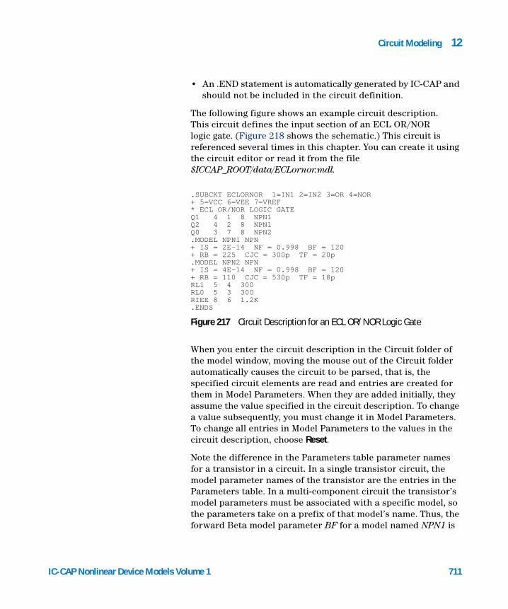
Circuit Modeling 12
IC-CAP Nonlinear Device Models Vo
• An .END statement is automatically generated by IC-CAP and should not be included in the circuit definition.
The following figure shows an example circuit description. This circuit defines the input section of an ECL OR/NOR logic gate. (Figure 218 shows the schematic.) This circuit is referenced several times in this chapter. You can create it using the circuit editor or read it from the file $ICCAP_ROOT/data/ECLornor.mdl.
When you enter the circuit description in the Circuit folder of the model window, moving the mouse out of the Circuit folder automatically causes the circuit to be parsed, that is, the specified circuit elements are read and entries are created for them in Model Parameters. When they are added initially, they assume the value specified in the circuit description. To change a value subsequently, you must change it in Model Parameters. To change all entries in Model Parameters to the values in the circuit description, choose Reset.
Note the difference in the Parameters table parameter names for a transistor in a circuit. In a single transistor circuit, the model parameter names of the transistor are the entries in the Parameters table. In a multi-component circuit the transistor’s model parameters must be associated with a specific model, so the parameters take on a prefix of that model’s name. Thus, the forward Beta model parameter BF for a model named NPN1 is
.SUBCKT ECLORNOR 1=IN1 2=IN2 3=OR 4=NOR+ 5=VCC 6=VEE 7=VREF* ECL OR/NOR LOGIC GATEQ1 4 1 8 NPN1Q2 4 2 8 NPN1Q0 3 7 8 NPN2.MODEL NPN1 NPN+ IS = 2E-14 NF = 0.998 BF = 120+ RB = 225 CJC = 300p TF = 20p.MODEL NPN2 NPN+ IS = 4E-14 NF = 0.998 BF = 120+ RB = 110 CJC = 530p TF = 18pRL1 5 4 300RL0 5 3 300RIEE 8 6 1.2K.ENDS
Figure 217 Circuit Description for an ECL OR/NOR Logic Gate
lume 1 711
712
12 Circuit Modeling
listed in the Parameter Editor as NPN1.BF. In the example above, transistors Q1 and Q2 both use the NPN1 model, while transistor Q0 uses the NPN2 model.
IC-CAP Nonlinear Device Models Volume 1
Circuit Modeling 12
Circuit Measurement
IC-CAP Nonlinear Device Models Vo
The process of measuring a circuit in IC-CAP is identical to measuring a single device. The circuit stimuli and responses are specified in the input and output tables, respectively, of the Measure/Simulate folder. You can perform a measurement by clicking Measure in the Measure/Simulate folder the DUT or Setup levels. In performing measurements on circuits, there are several additional items not found in single component measurement.
Multiple Instrument Names
In measuring a single component, it is common to use only one DC source and measurement instrument because only four terminals are involved. The typical circuit can have more than four terminals and require several DC source and measurement instruments. Any number of instruments of the same or similar type can be connected to the circuit under test as long as they are entered in Hardware Setup. When using multiple instruments, each of their units must have a unique name.
Isolating Circuit Elements for Measurement and Extraction
The characterization of a circuit may require the measurement and modeling of several sub-circuit elements. The accuracy of the sub-circuit model generated is dependent upon how well that circuitry can be isolated from the rest of the overall circuit.
Examine the simplified schematic of the input to an ECL OR/NOR gate in the following figure. The input stage of this circuit is a differential amplifier with a collector resistor in each leg and a resistor for a current source. It is possible to characterize the individual transistors in this circuit by selectively biasing only the terminals that make it active and that keep other parts of the circuit in an off or latent state. In this case, biasing IN1, VCC, and VEE turns on the circuit that contains RL1, Q1, and RIEE. These components have now been isolated so that their model parameters can be extracted. This type of selective measurement allows characterization of individual or small groups of sub-circuit elements.
lume 1 713
714
12 Circuit Modeling
Figure 218 ECL OR/NOR Schematic Diagram
IC-CAP Nonlinear Device Models Volume 1

Circuit Modeling 12
Circuit Parameter Extraction
IC-CAP Nonlinear Device Models Vo
Circuit parameter extraction is identical to single component parameter extraction through the use of Transforms. However, because circuits are custom in nature, most of the extraction routines must also be custom designed. With the availability of the Program function and optimize transforms, this is simple and quick to evaluate and execute. The critical factor in a successful circuit level parameter extraction is the ability to make a measurement and subsequent extraction involving only the dominant component parameters.
For a full model extraction of a single component, you will attain more accuracy if that device is available without any additional components connected to it. For most functional block level circuits however, a subset of the transistor model parameters is usually sufficient for studying circuit behavior.
Extracting Transistor Parameters Using Library Functions
In the explanation of a selective measurement on a sub-portion of a circuit in the previous section, Q1 and its neighboring resistors were isolated in the ECL logic gate. The forward active model parameters can be extracted from this measurement using the model extraction functions in the function list or by setting up a custom optimization. To access the functions, add transforms that use them to a setup that contains the measurement. It is possible to use the provided transistor extraction functions to obtain model parameters for devices connected into a larger circuit.Because all models in a circuit have model parameters in the Parameters table with the model’s name as a prefix, IC-CAP must be told which model to use with the extraction transforms. This is easily done by setting a variable in the model level variable table. Enter a variable in the table called EXTR_MODEL and set its value to the name of the transistor whose parameters are being extracted. When the extraction transforms are executed, IC-CAP refers to the correct Parameters table entry as it writes the extracted value back to
lume 1 715
716
12 Circuit Modeling
the table. For example, to use a function list transform on the model NPN1 mentioned above, add the following to the model level variable table: EXTR_MODEL NPN1
Each time another transistor is used for an extraction, place its name in the value field. A more efficient method of extracting individual transistor models is to create an individual setup for each device. The variable table at the setup level can then include the EXTR_MODEL entry, keeping the transistor extraction local to that setup. This can also be done in an analogous way at the DUT level.
It is sometimes necessary to specify the particular DUT in a circuit that should be used in an extraction routine. For example, in a circuit that contains two MOSFETs there are two different sets of geometry parameters (L and W). For the extraction to work correctly, the EXTR_DUT variable must be set to the name of the transistor with the correct geometry parameters. Therefore, to characterize transistor M1, which uses model NMOS1, add the following to the model level variable table:
EXTR_DUT M1EXTR_MODEL NMOS1
Situations where EXTR_DUT must be set can also arise when test circuits are defined. In this case, DUT parameters that normally appear without a prefix in the DUT Parameters table will include the transistor name from the Test Circuit as a prefix. For the extractions to use these parameters, EXTR_DUT must be set to the transistor name that is used in the test circuit.
Extracting Parameters Through Optimization
It is not always possible to adequately isolate a circuit component before using a standard extraction function. In these cases it is still possible to extract model parameters by using the optimize function. As with any extraction function, successful use of the optimizer requires that the parameters being optimized have a dominant effect over the simulation of the
IC-CAP Nonlinear Device Models Volume 1
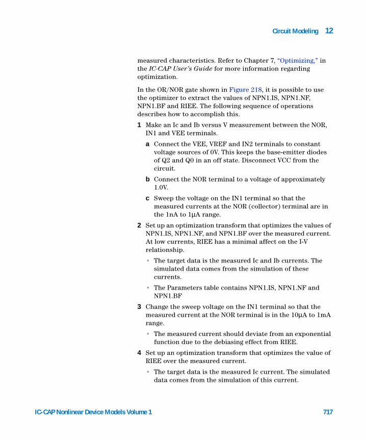
Circuit Modeling 12
IC-CAP Nonlinear Device Models Vo
measured characteristics. Refer to Chapter 7, “Optimizing,” in the IC-CAP User’s Guide for more information regarding optimization.
In the OR/NOR gate shown in Figure 218, it is possible to use the optimizer to extract the values of NPN1.IS, NPN1.NF, NPN1.BF and RIEE. The following sequence of operations describes how to accomplish this.
1 Make an Ic and Ib versus V measurement between the NOR, IN1 and VEE terminals.
a Connect the VEE, VREF and IN2 terminals to constant voltage sources of 0V. This keeps the base-emitter diodes of Q2 and Q0 in an off state. Disconnect VCC from the circuit.
b Connect the NOR terminal to a voltage of approximately 1.0V.
c Sweep the voltage on the IN1 terminal so that the measured currents at the NOR (collector) terminal are in the 1nA to 1µA range.
2 Set up an optimization transform that optimizes the values of NPN1.IS, NPN1.NF, and NPN1.BF over the measured current. At low currents, RIEE has a minimal affect on the I-V relationship.
• The target data is the measured Ic and Ib currents. The simulated data comes from the simulation of these currents.
• The Parameters table contains NPN1.IS, NPN1.NF and NPN1.BF
3 Change the sweep voltage on the IN1 terminal so that the measured current at the NOR terminal is in the 10µA to 1mA range.
• The measured current should deviate from an exponential function due to the debiasing effect from RIEE.
4 Set up an optimization transform that optimizes the value of RIEE over the measured current.
• The target data is the measured Ic current. The simulated data comes from the simulation of this current.
lume 1 717
718
12 Circuit Modeling
• The Parameters table contains only the circuit element RIEE.
After each of these measurements and optimizations has been executed, the Model Parameters table is updated with the extracted values of these elements.
IC-CAP Nonlinear Device Models Volume 1
Circuit Modeling 12
Circuit Simulation
IC-CAP Nonlinear Device Models Vo
Circuit simulation is performed identically to single device simulation. The circuit usually has more inputs and outputs defined than a single device. In addition, the simulated circuit can use independent or controlled voltage and current sources that are defined within the Circuit Editor. When IC-CAP simulates a circuit, it first builds a complete SPICE deck from the circuit description and the setup table. The source names are built from the source type (V or I) and the nodes to which they are connected. Use of the simulation debugger can improve efficiency in performing successful simulations. Knowledge of how IC-CAP interacts with the SPICE simulators gives you more control over the options available for circuit simulation. For more information, refer to Chapter 3, “SPICE Simulators,” in the Reference.
One of the advantages of simulating circuits through IC-CAP is the increased levels of analysis available. IC-CAP allows a sweep of more parameters than with a stand-alone SPICE simulator. For example, it is possible to simulate a circuit’s behavior over bias conditions, component values and temperature in the same simulation. Once a simulation is complete, you may further analyze the stimulus and response data with IC-CAP’s numerical and graphic capabilities. The two-port simulation features enable you to study the high-frequency characteristics of a circuit using any of the S, H, Y, or Z 2-port parameters.
Design Optimization
Designing a circuit usually follows a path of defining a block level functional description, translating it into discrete circuit components, then optimizing those components for the required performance. This last stage can be simplified with the IC-CAP system. It is possible to specify the desired performance from a
lume 1 719
720
12 Circuit Modeling
circuit and then let the IC-CAP optimizer find the best component and model parameters to satisfy it. The following is an overview of how to do this.
1 Enter a circuit with a first order estimate of the required parameters and component values.
2 Create a setup with the inputs and outputs that simulate the desired region of performance.
3 Simulate the circuit to create a set(s) of output data.
4 Copy the simulated data into the measured data set(s) in the outputs.
a Type the letter S in the Type field and press Return.
b Type the letter B in the same field to replace the letter S.
5 Save the desired outputs to files using the Write to File menu choice on each output.
6 Edit the files using any editor. Scan down the file to find the type MEAS data section. This is where the measured data begins. Edit the output values, replacing them with the desired performance values for the circuit. Save the file when done.
7 Read the file (and thus the new data) back into the outputs in IC-CAP using the Read from file command on the desired outputs.
8 Set up an optimization transform to find the required parameter and component values that best match the new measured data.
This type of design optimization can save many hours of iteration in fine-tuning high-performance circuit designs.
IC-CAP Nonlinear Device Models Volume 1
Circuit Modeling 12
Test Circuits
IC-CAP Nonlinear Device Models Vo
When measuring a single device or a complex circuit you often require additional components for biasing, setting operating points, or tuning the high-frequency performance characteristics. Even when no additional components are required, there may still be some parasitic elements introduced by the connections of the device to the instrumentation. Examples of this are DC resistance in probe-to-wafer contacts, inductances in IC package bond wires, and the shunt resistances in the bias ports of network analyzers. The Test Circuit in IC-CAP allows you to include these elements when performing a simulation or optimization without including them in the main circuit description or device model.
Syntax
A circuit editor is available for each DUT. To access it, select Edit in the DUT Circuit folder. This produces a window that has both the DUT Parameters table and the test circuit editor. The mechanics of using this editor are the same as using the circuit editor.
The test circuit adds another level of circuit hierarchy to the overall system being measured and modeled. It is implemented through a circuit description that uses the SPICE subcircuit syntax. The example test circuit shown in the following figure adds a capacitor and resistor to the outputs of the ECL logic gate described earlier.
* Resistive / Capacitive circuits to * simulate the effect of gate loading .SUBCKT gateload 1=IN1 2=IN2 3=OR + 4=NOR 5=VCC 6=VEE 7=VREFXornor 1 2 3 4 5 6 7 ECLornorCor 3 0 1pRor 3 0 10MEGCnor 4 0 1pRnor 4 0 10MEG.ENDS
Figure 219 Test Circuit for an ECL Logic Gate
lume 1 721
722
12 Circuit Modeling
This test circuit is added to the SPICE circuit deck each time a simulation is called or when an optimization that uses a SPICE simulation is performed. It does not modify the original model description in any way. The values of the elements in the test circuit can be modified in the DUT Model Parameters.
IC-CAP Nonlinear Device Models Volume 1
Circuit Modeling 12
Hierarchical Modeling
IC-CAP Nonlinear Device Models Vo
The previous test circuit section on illustrated one way to include hierarchy in an overall circuit description. The test circuit, however, is at the highest level of hierarchy in an IC-CAP circuit. It is also possible to build a complete circuit by combining smaller circuit or transistor models into one subcircuit definition. This way, you can update the models of smaller subcircuits or individual components and have these changes automatically propagate into all circuits that use it.
Circuits Built from Sub-models
The ECL logic gate defined in Figure 218 uses two sizes of NPN transistors. Each transistor has a separate .MODEL card associated with it. These transistor model definitions can be removed from the logic gate circuit and reference other models currently active in IC-CAP. When a simulation is performed, IC-CAP includes these device models in the circuit definition.
To use external models, the models that you want to include must be in the IC-CAP model list. In the circuit definition that uses these model references, remove the .MODEL card. The model name used for the transistors should then be the same as the names in the IC-CAP model list. To use this technique for the ECL logic gate, read in models for the NPN1 and NPN2 transistors into IC-CAP. Then delete the two model cards in the logic gate circuit. The resulting model list and circuit description are shown in the following 2 figures.
This approach provides flexibility. It allows you to keep a standard library of device models to include in larger circuits requiring accurate device models. This allows you to quickly cut-and-paste different component models into circuits and compare performance. It also greatly reduces the size of the circuit definition that needs to be maintained.
lume 1 723
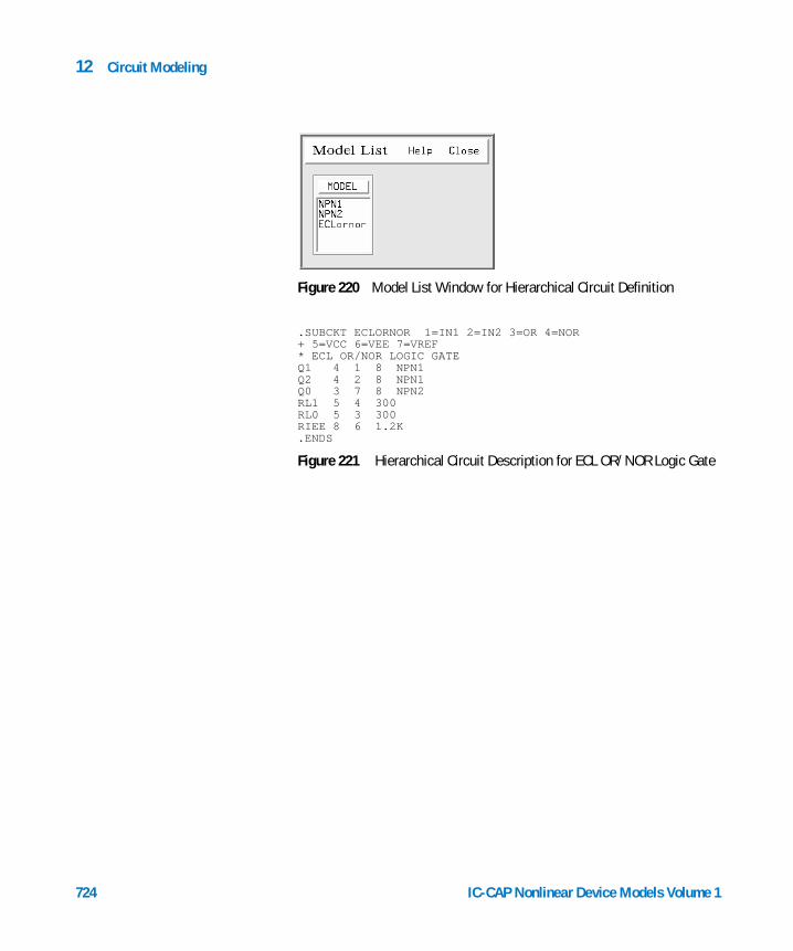
724
12 Circuit Modeling
Figure 220 Model List Window for Hierarchical Circuit Definition
.SUBCKT ECLORNOR 1=IN1 2=IN2 3=OR 4=NOR+ 5=VCC 6=VEE 7=VREF* ECL OR/NOR LOGIC GATEQ1 4 1 8 NPN1Q2 4 2 8 NPN1Q0 3 7 8 NPN2RL1 5 4 300RL0 5 3 300RIEE 8 6 1.2K.ENDS
Figure 221 Hierarchical Circuit Description for ECL OR/NOR Logic Gate
IC-CAP Nonlinear Device Models Volume 1
Circuit Modeling 12
Functional Circuit Blocks
IC-CAP Nonlinear Device Models Vo
Previous sections in this chapter provided different aspects of the use of IC-CAP for modeling complete functional circuits. This section provides detailed examples of circuit models and custom model extractions you can create. These examples are provided to stimulate ideas for using IC-CAP to meet specific circuit modeling requirements.
Types of Circuits in IC-CAP
The types of circuits for measurement and simulation with IC-CAP are unlimited. Anything that can be simulated on a stand-alone SPICE simulator can be simulated with IC-CAP. In fact, any type of system that can be measured with the IC-CAP library of instruments can be characterized.
With the variety of components supported by SPICE, IC-CAP can be used to both characterize and design circuit modules. Classical examples of both single device and functional circuit modeling problems that are easily solved with IC-CAP are included.
Modeling the Reverse Active Region of an NPN Transistor
One of the constant sources of error in modeling the performance of a reverse active NPN transistor is the parasitic PNP formed by the base, collector, and substrate of the integrated structure. (This was briefly described in “PNP Transistors” on page 577.) A simple solution to modeling this region of operation is to use the complete functional circuit displayed in the following figure.
lume 1 725
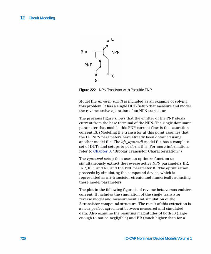
726
12 Circuit Modeling
Model file npnwpnp.mdl is included as an example of solving this problem. It has a single DUT/Setup that measure and model the reverse active operation of an NPN transistor.
The previous figure shows that the emitter of the PNP steals current from the base terminal of the NPN. The single dominant parameter that models this PNP current flow is the saturation current IS. (Modeling the transistor at this point assumes that the DC NPN parameters have already been obtained using another model file. The bjt_npn.mdl model file has a complete set of DUTs and setups to perform this. For more information, refer to Chapter 8, “Bipolar Transistor Characterization.”)
The rgummel setup then uses an optimize function to simultaneously extract the reverse active NPN parameters BR, IKR, ISC, and NC and the PNP parameter IS. The optimization proceeds by simulating the compound device, which is represented as a 2-transistor circuit, and numerically adjusting these model parameters.
The plot in the following figure is of reverse beta versus emitter current. It includes the simulation of the single transistor reverse model and measurement and simulation of the 2-transistor compound structure. The result of this extraction is a near perfect agreement between measured and simulated data. Also examine the resulting magnitudes of both IS (large enough to not be negligible) and BR (much higher than for a
Figure 222 NPN Transistor with Parasitic PNP
IC-CAP Nonlinear Device Models Volume 1
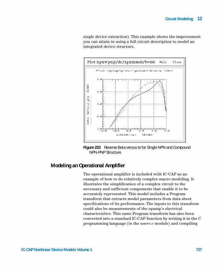
Circuit Modeling 12
IC-CAP Nonlinear Device Models Vo
single device extraction). This example shows the improvement you can attain in using a full circuit description to model an integrated device structure.
Figure 223 Reverse Beta versus Ie for Single NPN and Compound NPN-PNP Structure
Modeling an Operational Amplifier
The operational amplifier is included with IC-CAP as an example of how to do relatively complex macro modeling. It illustrates the simplification of a complex circuit to the necessary and sufficient components that enable it to be accurately represented. This model includes a Program transform that extracts model parameters from data sheet specifications of its performance. The inputs to this transform could also be measurements of the opamp’s electrical characteristics. This same Program transform has also been converted into a standard IC-CAP function by writing it in the C programming language (in the userc.c module) and compiling
lume 1 727
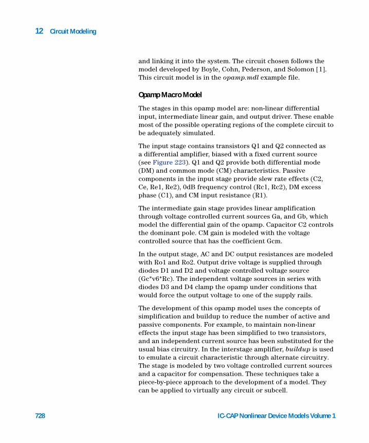
728
12 Circuit Modeling
and linking it into the system. The circuit chosen follows the model developed by Boyle, Cohn, Pederson, and Solomon [1]. This circuit model is in the opamp.mdl example file.
Opamp Macro Model
The stages in this opamp model are: non-linear differential input, intermediate linear gain, and output driver. These enable most of the possible operating regions of the complete circuit to be adequately simulated.
The input stage contains transistors Q1 and Q2 connected as a differential amplifier, biased with a fixed current source (see Figure 223). Q1 and Q2 provide both differential mode (DM) and common mode (CM) characteristics. Passive components in the input stage provide slew rate effects (C2, Ce, Re1, Re2), 0dB frequency control (Rc1, Rc2), DM excess phase (C1), and CM input resistance (R1).
The intermediate gain stage provides linear amplification through voltage controlled current sources Ga, and Gb, which model the differential gain of the opamp. Capacitor C2 controls the dominant pole. CM gain is modeled with the voltage controlled source that has the coefficient Gcm.
In the output stage, AC and DC output resistances are modeled with Ro1 and Ro2. Output drive voltage is supplied through diodes D1 and D2 and voltage controlled voltage source (Gc*v6*Rc). The independent voltage sources in series with diodes D3 and D4 clamp the opamp under conditions that would force the output voltage to one of the supply rails.
The development of this opamp model uses the concepts of simplification and buildup to reduce the number of active and passive components. For example, to maintain non-linear effects the input stage has been simplified to two transistors, and an independent current source has been substituted for the usual bias circuitry. In the interstage amplifier, buildup is used to emulate a circuit characteristic through alternate circuitry. The stage is modeled by two voltage controlled current sources and a capacitor for compensation. These techniques take a piece-by-piece approach to the development of a model. They can be applied to virtually any circuit or subcell.
IC-CAP Nonlinear Device Models Volume 1
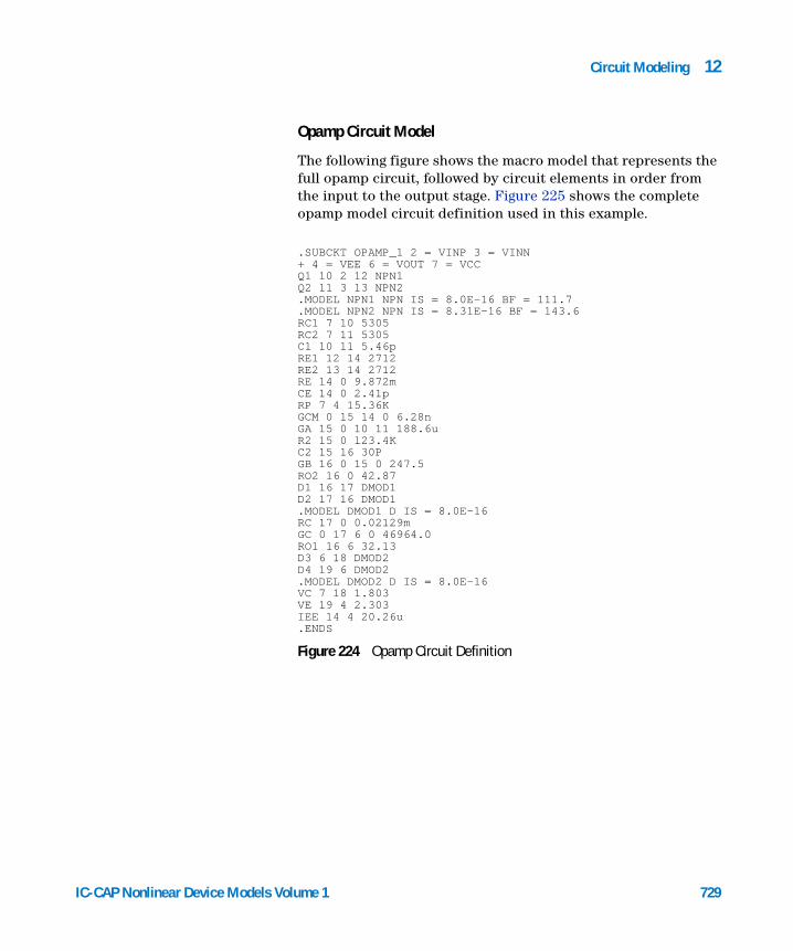
Circuit Modeling 12
IC-CAP Nonlinear Device Models Vo
Opamp Circuit Model
The following figure shows the macro model that represents the full opamp circuit, followed by circuit elements in order from the input to the output stage. Figure 225 shows the complete opamp model circuit definition used in this example.
.SUBCKT OPAMP_1 2 = VINP 3 = VINN+ 4 = VEE 6 = VOUT 7 = VCCQ1 10 2 12 NPN1Q2 11 3 13 NPN2.MODEL NPN1 NPN IS = 8.0E-16 BF = 111.7.MODEL NPN2 NPN IS = 8.31E-16 BF = 143.6RC1 7 10 5305RC2 7 11 5305C1 10 11 5.46pRE1 12 14 2712RE2 13 14 2712RE 14 0 9.872mCE 14 0 2.41pRP 7 4 15.36KGCM 0 15 14 0 6.28nGA 15 0 10 11 188.6uR2 15 0 l23.4KC2 15 16 30PGB 16 0 15 0 247.5RO2 16 0 42.87D1 16 17 DMOD1D2 17 16 DMOD1.MODEL DMOD1 D IS = 8.0E-16RC 17 0 0.02129mGC 0 17 6 0 46964.0RO1 16 6 32.13D3 6 18 DMOD2D4 19 6 DMOD2.MODEL DMOD2 D IS = 8.0E-16VC 7 18 1.803VE 19 4 2.303IEE 14 4 20.26u.ENDS
Figure 224 Opamp Circuit Definition
lume 1 729
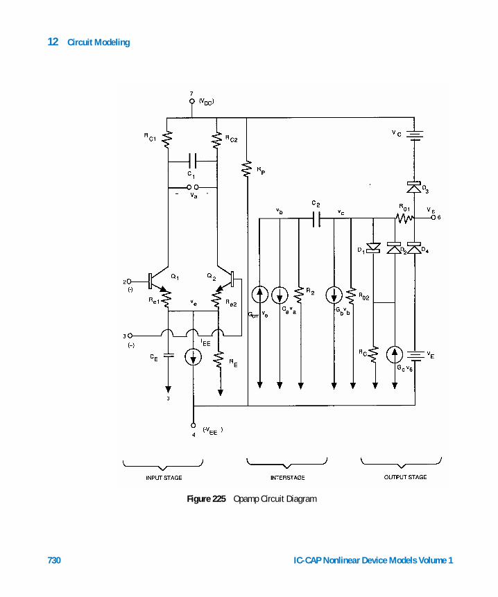
730
12 Circuit Modeling
Figure 225 Opamp Circuit Diagram
IC-CAP Nonlinear Device Models Volume 1
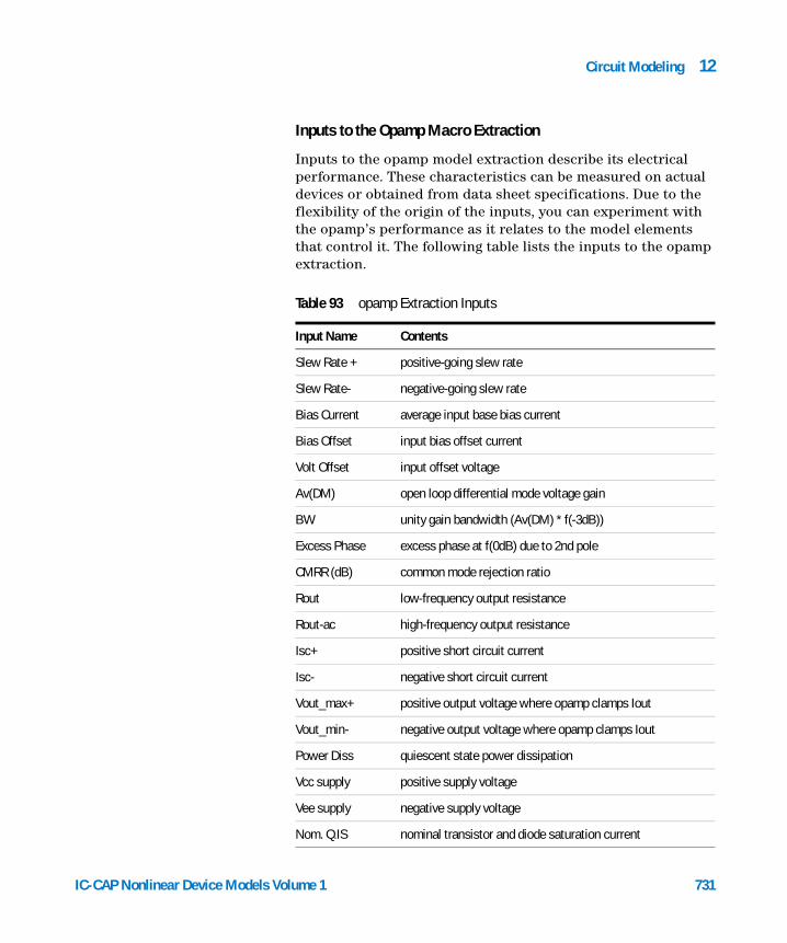
Circuit Modeling 12
IC-CAP Nonlinear Device Models Vo
Inputs to the Opamp Macro Extraction
Inputs to the opamp model extraction describe its electrical performance. These characteristics can be measured on actual devices or obtained from data sheet specifications. Due to the flexibility of the origin of the inputs, you can experiment with the opamp’s performance as it relates to the model elements that control it. The following table lists the inputs to the opamp extraction.
Table 93 opamp Extraction Inputs
Input Name Contents
Slew Rate + positive-going slew rate
Slew Rate- negative-going slew rate
Bias Current average input base bias current
Bias Offset input bias offset current
Volt Offset input offset voltage
Av(DM) open loop differential mode voltage gain
BW unity gain bandwidth (Av(DM) * f(-3dB))
Excess Phase excess phase at f(0dB) due to 2nd pole
CMRR (dB) common mode rejection ratio
Rout low-frequency output resistance
Rout-ac high-frequency output resistance
Isc+ positive short circuit current
Isc- negative short circuit current
Vout_max+ positive output voltage where opamp clamps Iout
Vout_min- negative output voltage where opamp clamps Iout
Power Diss quiescent state power dissipation
Vcc supply positive supply voltage
Vee supply negative supply voltage
Nom. Q.IS nominal transistor and diode saturation current
lume 1 731
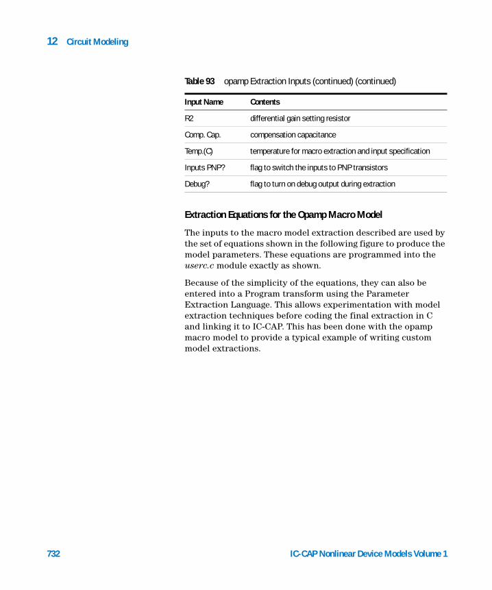
732
12 Circuit Modeling
Extraction Equations for the Opamp Macro Model
The inputs to the macro model extraction described are used by the set of equations shown in the following figure to produce the model parameters. These equations are programmed into the userc.c module exactly as shown.
Because of the simplicity of the equations, they can also be entered into a Program transform using the Parameter Extraction Language. This allows experimentation with model extraction techniques before coding the final extraction in C and linking it to IC-CAP. This has been done with the opamp macro model to provide a typical example of writing custom model extractions.
R2 differential gain setting resistor
Comp. Cap. compensation capacitance
Temp.(C) temperature for macro extraction and input specification
Inputs PNP? flag to switch the inputs to PNP transistors
Debug? flag to turn on debug output during extraction
Table 93 opamp Extraction Inputs (continued) (continued)
Input Name Contents
IC-CAP Nonlinear Device Models Volume 1

Circuit Modeling 12
IC-CAP Nonlinear Device Models Vo
Bias Circuitry
The opamp model, fully defined and model parameters extracted, can now be used as a functional circuit block. This requires that the opamp be biased with external supply voltages and circuit configuring components. This was demonstrated previously through the use of a test circuit. The test circuit implemented forms an inverting amplifier using an input and feedback resistor with the opamp. This results in a complete functional circuit whose performance can be studied in more detail. The test circuit definition and the resulting equivalent circuit are shown in the following 2 figures.
Figure 226 C Coded Opamp Extraction Equations
)pos. and neg. slew-rates are interchanged in calculations */ sr_plus ; sr_plus = sr_neg ; sr_neg = tmp ; 3 * (temp/27);p + isc_n ) / 2 ; isd4 = is ;1.0E6; /* convert slew rates to Volts/sec */.0E6;(c2/2) * sr_plus ;r_neg - c2 ;bos/2 ; /* ib2-ib1 = ib+ - ib- = ibos */bos/2 ;
ents will have opposite signs with pnp input stage */ -ib1 ; ib2 = -ib2 ; ib1 ;ib2 ;a1+1 )/beta1 + (beta2+1)/beta2 ) * ic1 ; ;( 1 + vos/vt ) ; ;1 / ( 2*M_PI*fOdB*c2 ) ;(beta1+beta2) / (beta1+beta2+2) * (rc1 - 1/gm1) ;* tan(delta_phi) ;fined as being a positive value & Vee as a negative value */) * (vcc-vee) / (pd - fabs(vcc*2*ic1) - fabs(vee * iee) ) ;
0.0,cmrr/20.0); /* convert from dB to decimal */c1*cmrr) ;c ; ro1 ;c1 / ( r2 * ro2 ) ;c1) * gb * r2 - isc ;= ix * exp( -ro1*isc/vt ) ;00*ix) * log ( ix/isd1 ) ;
c) - vout_p + vt*log(isc_p/isd3) ;e) + vout_n + vt*log(isc_n/isd4) ;
if ( is_pnp /* for pnp, tmp =vt = 25.85E-isc = ( isc_is1 = isd3 =sr_plus * = sr_neg * = 1ic1 = ic2 = ce = 2*ic1/sib2 = ib + iib1 = ib - iif (is_pnp)/* bias curr ib1 =beta1 = ic1/beta2 = ic2/iee = (( betre = 200/ieeis2 = is1 * gm1 = ic1/vtrc2 = rc1 = re1 = re2 = c1 = c2 / 2 /* Vcc is derp = vcc-veega = 1/rc1;cmrr = pow(1gcm = 1 / (rro1 = rout_aro2 = rout -gb = avd * rix = ( 2 * iisd1 = isd2 rc = vt / (1gc= 1/rc;vc = fabs(vcve = fabs(ve
lume 1 733
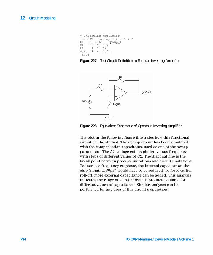
734
12 Circuit Modeling
The plot in the following figure illustrates how this functional circuit can be studied. The opamp circuit has been simulated with the compensation capacitance used as one of the sweep parameters. The AC voltage gain is plotted versus frequency with steps of different values of C2. The diagonal line is the break point between process limitations and circuit limitations. To increase frequency response, the internal capacitor on the chip (nominal 30pF) would have to be reduced. To force earlier roll-off, more external capacitance can be added. This analysis indicates the range of gain-bandwidth product available for different values of capacitance. Similar analyses can be performed for any area of this circuit’s operation.
* Inverting Amplifier.SUBCKT inv_amp 1 2 3 4 6 7X1 2 3 4 6 7 opamp_1Rf 6 2 10KRin 2 1 2KRgnd 3 0 1.0m.ENDS
Figure 227 Test Circuit Definition to Form an Inverting Amplifier
Figure 228 Equivalent Schematic of Opamp in Inverting Amplifier
-
+
RgndVin
Rin
Rf
Vout
IC-CAP Nonlinear Device Models Volume 1

Circuit Modeling 12
IC-CAP Nonlinear Device Models Vo
Figure 229 AC Opamp Response vs C2 Capacitance
lume 1 735

12 Circuit Modeling
References
736
1 G.R. Boyle, B.M. Cohn, D.O.Pederson, J.E. Solomon. Macromodeling of Integrated Circuit Operational Amplifiers, IEEE Journal of Solid-State Circuits, Vol. SC-9, No. 6, December 1974.
IC-CAP Nonlinear Device Models Volume 1
Agilent 85190A IC-CAP 2008Nonlinear Device Models Volume 1
131/f Noise Extraction Toolkit
Types of Noise 738
The Significance of 1/f Noise 739
1/f (Flicker Noise) Modeling 740
Noise Measurement Setup 743
Parameter Extraction Procedure 745
1/f Noise Toolkit Description 748
Opening the 1/f Toolkit 749
System Settings 752
General Settings 754
Verify DC 760
Measure Noise 765
1/f Noise Extraction with MOS Transistors 784
The 1/f Noise Extraction Toolkit runs with a GUI. The Toolkit can measure and extract 1/f noise parameters.
737Agilent Technologies
13 1/f Noise Extraction Toolkit
Types of Noise
738
The main sources of noise in semiconductor devices are:
1 Thermal Noise is due to the Johnson effect in the ohmic regions. It is practically frequency independent.
2 Shot Noise is due the diffusion and passage of carriers across barriers. This noise can be represented by independent random events. Its spectral distribution depends on the bias current and is frequency independent.
3 Burst Noise is due to the capture and emission of carriers in localized traps causing a fluctuation between current levels. It is usually present in small devices and Si-SiO2 interfaces (e.g. MOS).
4 1/f Noise (also called Flicker Noise) is believed to be caused by surface recombination due to traps and defects in the crystal.
IC-CAP Nonlinear Device Models Volume 1
1/f Noise Extraction Toolkit 13
The Significance of 1/f Noise
IC-CAP Nonlinear Device Models Vo
Due to their broadband spectral distribution, thermal and shot noise contribute to the circuit noise figure. The circuit (in terms of bias, gain, matching networks, etc.) is usually optimized to minimize or lower the noise figure.
Although the 1/f noise is generated at low frequencies, its contribution to the overall noise can be very significant to some RF circuits since its spectral power density is up converted in the band of interest by circuit nonlinearities. This is especially true in mixers and oscillators.
lume 1 739
13 1/f Noise Extraction Toolkit
1/f (Flicker Noise) Modeling
740
The state of the art of 1/f noise modeling will be reviewed, and then the 1/f noise setup will be described with more details. The 1/f noise spectral power density is given by [8]:
(132)
where Kf and Af are the model parameters that needs to be extracted, I is the current flowing through the junction where the flicker noise is generated. The figure below shows the small signal equivalent circuits of bipolar and MOS transistors. All the noise sources, including thermal and shot, are represented. In bipolar transistors the noise is generated by the recombination current in the base, therefore . The 1/f noise is represented by the current source Inb. Its squared mean value is given by:
(133)
where B is the frequency band of interest.
In FET and MOS devices the noise is generated in the channel, therefore I = Ib. In the MOS equivalent circuit shown below, the 1/f noise is represented by the current source Ind. The expression for the density is:
(134)
The bipolar equivalent circuit used is shown below.
S1 f⁄ f( ) KfIAf
f-------⋅=
I Ib=
Inb2
⟨ ⟩ S1 f⁄ f( )df
B∫°=
S1 f⁄ f( ) Kf
IdAf
fEf
Cox Leff2⋅ ⋅
-------------------------------------⋅=
IC-CAP Nonlinear Device Models Volume 1
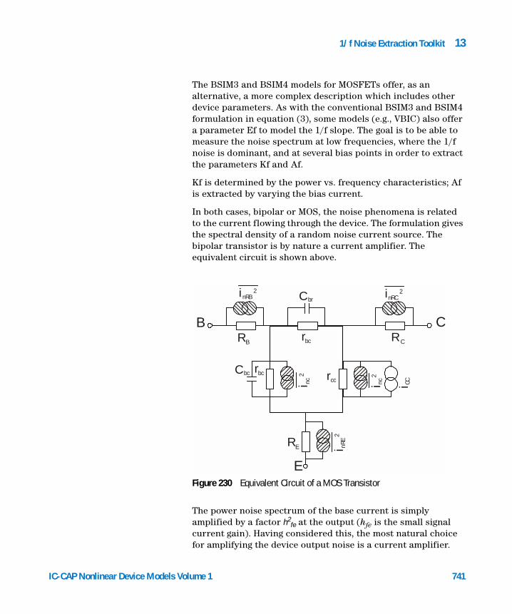
1/f Noise Extraction Toolkit 13
IC-CAP Nonlinear Device Models Vo
The BSIM3 and BSIM4 models for MOSFETs offer, as an alternative, a more complex description which includes other device parameters. As with the conventional BSIM3 and BSIM4 formulation in equation (3), some models (e.g., VBIC) also offer a parameter Ef to model the 1/f slope. The goal is to be able to measure the noise spectrum at low frequencies, where the 1/f noise is dominant, and at several bias points in order to extract the parameters Kf and Af.
Kf is determined by the power vs. frequency characteristics; Af is extracted by varying the bias current.
In both cases, bipolar or MOS, the noise phenomena is related to the current flowing through the device. The formulation gives the spectral density of a random noise current source. The bipolar transistor is by nature a current amplifier. The equivalent circuit is shown above.
The power noise spectrum of the base current is simply amplified by a factor h2
fe at the output (hfe is the small signal current gain). Having considered this, the most natural choice for amplifying the device output noise is a current amplifier.
Figure 230 Equivalent Circuit of a MOS Transistor
BR B
2inRB2inRC
C
C br
C bc rbc
rbc R C
2i nc
2i nR
ER E
E
i CCi nc
2 rcc
lume 1 741
742
13 1/f Noise Extraction Toolkit
The low noise current amplifier converts the output current noise into voltage. This avoids current to voltage conversions in the circuit. These conversions depend on other circuit parameters, and therefore introduce errors.
IC-CAP Nonlinear Device Models Volume 1
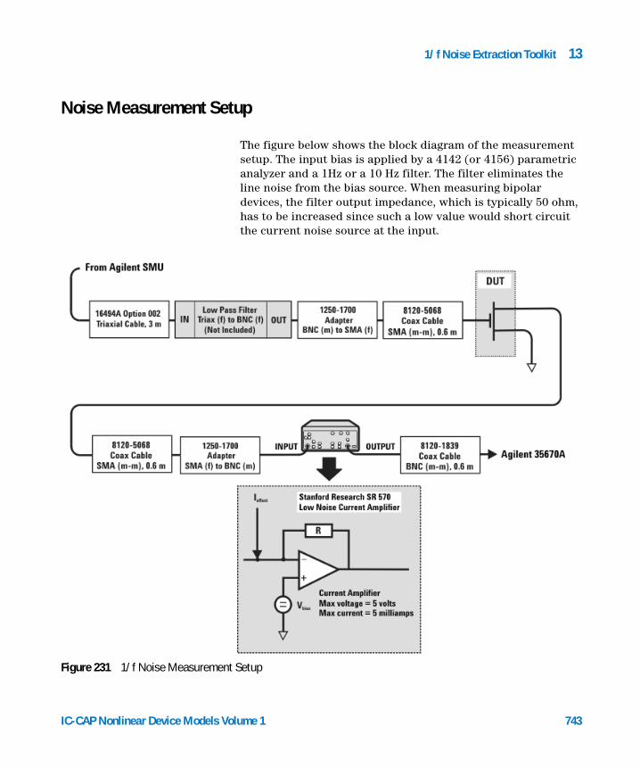
1/f Noise Extraction Toolkit 13
Noise Measurement Setup
IC-CAP Nonlinear Device Models Vo
The figure below shows the block diagram of the measurement setup. The input bias is applied by a 4142 (or 4156) parametric analyzer and a 1Hz or a 10 Hz filter. The filter eliminates the line noise from the bias source. When measuring bipolar devices, the filter output impedance, which is typically 50 ohm, has to be increased since such a low value would short circuit the current noise source at the input.
Figure 231 1/f Noise Measurement Setup
lume 1 743

744
13 1/f Noise Extraction Toolkit
The device output is directly connected to the SR570 low noise amplifier. Besides amplifying the output noise, the amplifier provides a current and a voltage supply which are used to bias the device output. The voltage supply allows the setting of the collector or drain voltage while the current source provides an offset current which is used to bias the device. The reason for using the current compensation is that the amplifier works best when the feedback current is minimal (the feedback current flows through R into the device to create the virtual null at the amplifier input). The SR570 can supply an output voltage of up to 5 V and a maximum current compensation of 5 mA.
The gain (expressed in terms of sensitivity A/V) can be varied between 10e-3 to 10e-12 A/V. For this application, since the amplifier bandwidth decreases with the sensitivity, only the higher sensitivities which ensure bandwidth of at least 1 KHz are actually used.
The device 1/f noise is amplified and measured by the 35670A dynamic signal analyzer. This instrument is ideal for analyzing signals with a low frequency power spectrum (such as 1/f noise) as opposed to a spectrum analyzer which is used at higher frequency bands. Because of the relatively low frequency range, the dynamic signal analyzer can directly sample the signal over a 1/f period and operate a FFT transform to calculate the spectral density.
IC-CAP Nonlinear Device Models Volume 1

1/f Noise Extraction Toolkit 13
Parameter Extraction Procedure
IC-CAP Nonlinear Device Models Vo
As mentioned already, to extract the noise parameters, Af and Kf, the 1/f noise spectral density of the noise current source needs to be measured at various bias points. Since the current amplifier does not have GP-IB control, its settings (bias voltage, current offset and sensitivity) have to be manually set at each bias point. The measurement is therefore semi-automated with the data acquisition and display controlled by IC-CAP. IC-CAP provides different model files for bipolar and MOS 1/f noise, but similar extraction procedures. The procedure consists of three steps and a verification phase.
In the BJT extraction, the Ic vs. Vbe DC traces are measured. This is accomplished by running the step Measure and Simulate DC Data in the GUI sequence. The DC current gain β, and the output conductance gce are calculated using the measured data.
In the MOS extraction, the Id vs. Vd DC traces are measured instead and the output conductance go is calculated.
Based on those data the user is asked to choose the bias points where the 1/f noise will be measured. Running the macro GUI step Measure Noise Data starts the interactive procedure for measuring the noise. For each bias point, the device is first biased at the base after some time that depends on the filter time constant. The operator is then asked to set the collector voltage, current offset and sensitivity on the SR570. The toolkit then calls the dynamic signal analyzer for measurement of the output noise. The spectral noise density at the output of the device is given by:
(135)
where Nmeas is the noise measured by the analyzer expressed in and SR570 is the sensitivity of the amplifier. In the bipolar case, assuming the DC beta is equal to the small signal current gain, the actual spectral power density of the base current noise source is given by:
Sic f⟨ ⟩ Nmeas SSR570×( )2=
V Hz⁄
lume 1 745

746
13 1/f Noise Extraction Toolkit
(136)
The third step is the extraction of the 1/f noise parameters. In the bipolar case, after selecting a set of traces at constant Vc, a macro linearizes equation (1) as follows:
and extracts the Af and Kf using a linear interpolation in the area where 1/f noise is present. Typically, the extraction is performed between 10 and 100 Hz of the 1/f band.
Sib f⟨ ⟩ Sic f⟨ ⟩ β2tr
⁄=
fSib f( )( )log Kf( ) Af Ib( )log+log=
Low pass filter
The filter schematic is shown in the figure below:
For Noise measurements of bipolar transistors, the low pass filter can be designed using an RC values network with a large output impedance (Ro = 330 kOhm). This large resistance prevents the noise voltage across the base of the transistor from being shorted out. Due to these large value, the filter series resistance is rather large, and so is the RC constant. This large resistance slows down the filter charge, and the device bias time is in the order of minutes. Also, the voltage across the filter might be several volts, therefore the input SMU voltage compliance must be set to a rather high value.
Ro10k10k10k10k
C1 C2 C1 C2 C1 C2
C1 = 100 F electolyticC2 = 100 pF ceramicR0 = 50 for CMOSRo = 330 k for bipolar
µ
ΩΩ
IC-CAP Nonlinear Device Models Volume 1

1/f Noise Extraction Toolkit 13
IC-CAP Nonlinear Device Models Vo
For Noise measurements of MOS transistors, the resistance Ro might be set to 50 ohm. The series resistances of the filter is 30k ohm, so that the filter charging will not be as long as in the bipolar case.
lume 1 747
13 1/f Noise Extraction Toolkit
1/f Noise Toolkit Description
748
• The Toolkit uses IC-CAP .mdm model files.
• The GUI layer uses advanced data management techniques for handling .mdm model files.
• New GUI interface leads the user through DC and Noise measurements and extraction.
• Dedicated transforms drive the 4142 or 4156.
System Parts List (Hardware)
• Stanford Research low noise amplifier LNA SR570.
• Agilent Dynamic Signal Analyzer (DSA) 35670A.
• Agilent 4142B or 4156B/C.
• Voltage DMM.
• 1 or 10 Hz low pass filter.
• Cables (BNC, triax).
• GSG probes for on-wafer measurement.
Software Requirements
• IC-CAP software. Agilent 85190A, revision 2001 or higher.
• DSA Driver. Agilent 3567A driver is the 85199G.
• IC-CAP Model Files (part of the new toolkit). These files are located in the directory examples/model_files/noise/1_f_toolkit.
• 1/f Noise Toolkit License for running Measurement and Extraction of these files.
IC-CAP Nonlinear Device Models Volume 1
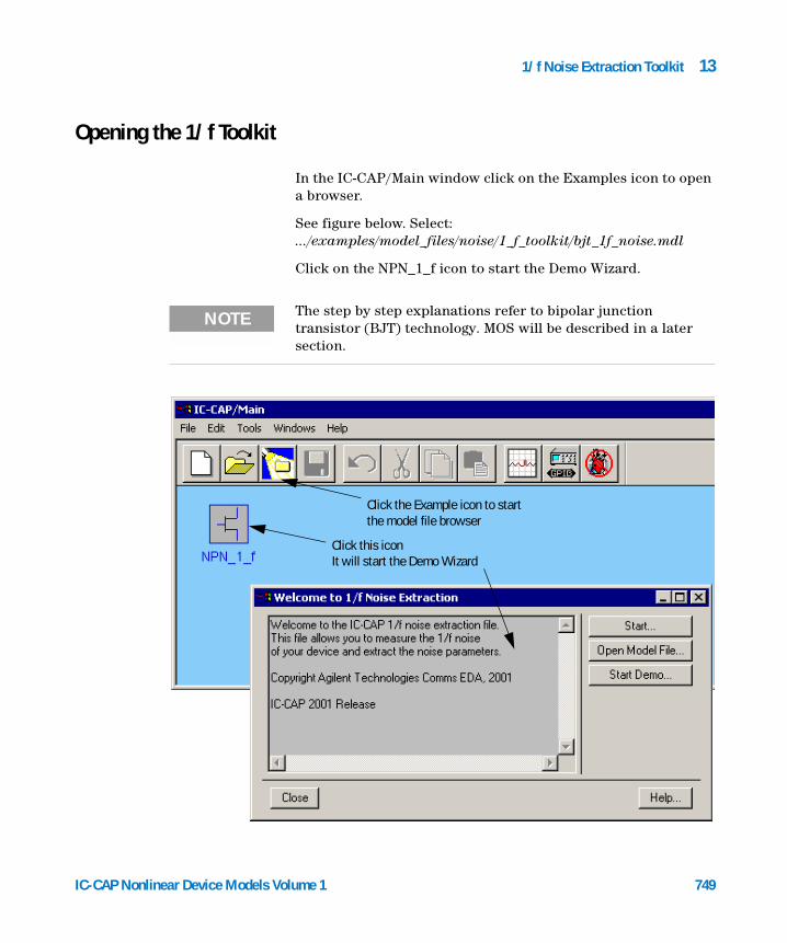
1/f Noise Extraction Toolkit 13
Opening the 1/f Toolkit
IC-CAP Nonlinear Device Models Vo
In the IC-CAP/Main window click on the Examples icon to open a browser.
See figure below. Select: .../examples/model_files/noise/1_f_toolkit/bjt_1f_noise.mdl
Click on the NPN_1_f icon to start the Demo Wizard.
NOTE The step by step explanations refer to bipolar junction transistor (BJT) technology. MOS will be described in a later section.
Click the Example icon to startthe model file browser
Click this iconIt will start the Demo Wizard
lume 1
749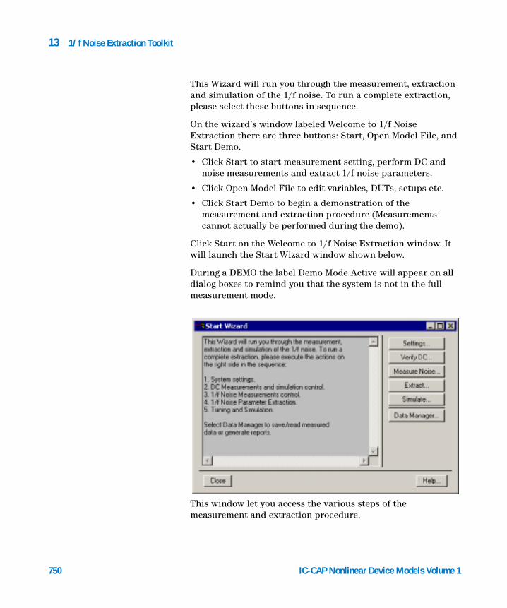
750
13 1/f Noise Extraction Toolkit
This Wizard will run you through the measurement, extraction and simulation of the 1/f noise. To run a complete extraction, please select these buttons in sequence.
On the wizard’s window labeled Welcome to 1/f Noise Extraction there are three buttons: Start, Open Model File, and Start Demo.
• Click Start to start measurement setting, perform DC and noise measurements and extract 1/f noise parameters.
• Click Open Model File to edit variables, DUTs, setups etc.
• Click Start Demo to begin a demonstration of the measurement and extraction procedure (Measurements cannot actually be performed during the demo).
Click Start on the Welcome to 1/f Noise Extraction window. It will launch the Start Wizard window shown below.
During a DEMO the label Demo Mode Active will appear on all dialog boxes to remind you that the system is not in the full measurement mode.
This window let you access the various steps of the measurement and extraction procedure.
IC-CAP Nonlinear Device Models Volume 1
1/f Noise Extraction Toolkit 13
IC-CAP Nonlinear Device Models Vo
• Click on Settings to access system settings (file notes and comments, bias settings, system hardware configuration and instrument option settings).
• Click on Verify DC to open the DC measurements wizard.
• Click on Measure Noise to open the Noise measurements wizard.
• Click on Extract to extract the noise parameters from selected measured data.
• Click on Simulate to compare measured and simulated noise and tune the extracted parameters.
• Click on Data Manager to read/save data and generate reports.
lume 1 751
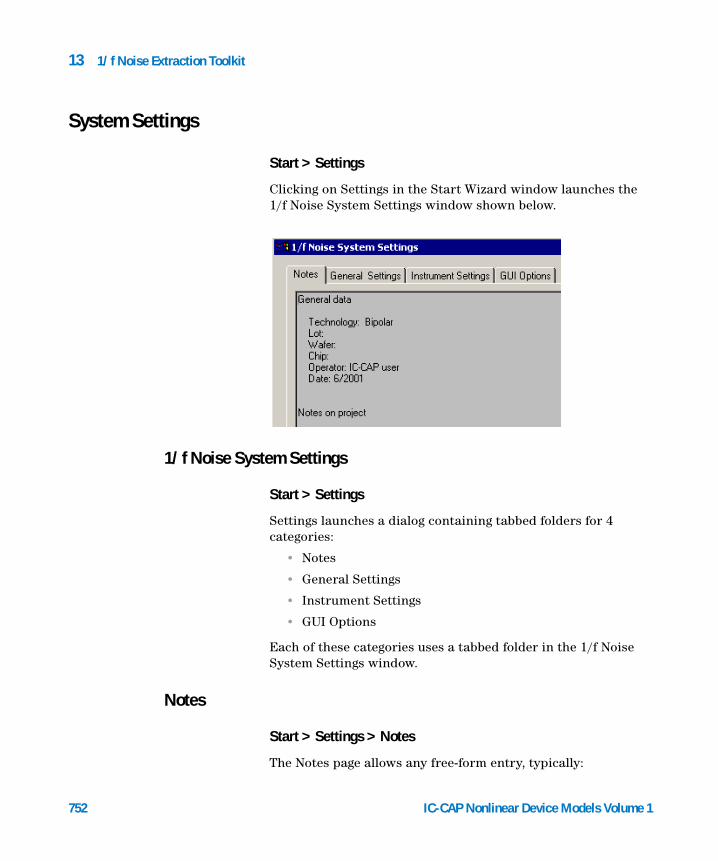
13 1/f Noise Extraction Toolkit
System Settings
752
Start > Settings
Clicking on Settings in the Start Wizard window launches the 1/f Noise System Settings window shown below.
1/f Noise System Settings
Start > Settings
Settings launches a dialog containing tabbed folders for 4 categories:
• Notes
• General Settings
• Instrument Settings
• GUI Options
Each of these categories uses a tabbed folder in the 1/f Noise System Settings window.
Notes
Start > Settings > Notes
The Notes page allows any free-form entry, typically:
IC-CAP Nonlinear Device Models Volume 1
1/f Noise Extraction Toolkit 13
IC-CAP Nonlinear Device Models Vo
• the technology,
• the source of the wafer, chip or package used for the test,
• the operator,
• data of special interest to this measurement,
• etc.
NOTE Any text entered on the Notes page will be printed in the final report.
In the Demo Mode the user is not allowed to change the input data (SMU settings) since this action would clear the measured data.
lume 1 753
13 1/f Noise Extraction Toolkit
General Settings
754
Start > Settings > General Settings
The Simulator Settings part of the dialog box allows
• Selection of a simulator, for example, hpspice or spectre.
• Specifying the Main Circuit File, Subcircuit File, and Parameter File. These are automatically loaded into the model file
CAUTION Changing the simulator will load new Circuit, Subcircuit, and Parameter files (if those are found). Previous data will be lost.
The IC-CAP General Settings part of the dialog box allows setting:
• Working Precision: this value must be at least set to 6, since the NDA frequency range must be saved with at least 6 figures.
• Min Log Value: defines the value to be used in a LOG plot, if data point value is zero or negative. Default is 1e−18 but for this application needs to be lowered to 1e−23.
• Retain Data: causes data from a Setup to be retained if a sweep changes but the number of points remains the same. Default in this application is Yes, which causes the data to be kept.
IC-CAP Nonlinear Device Models Volume 1
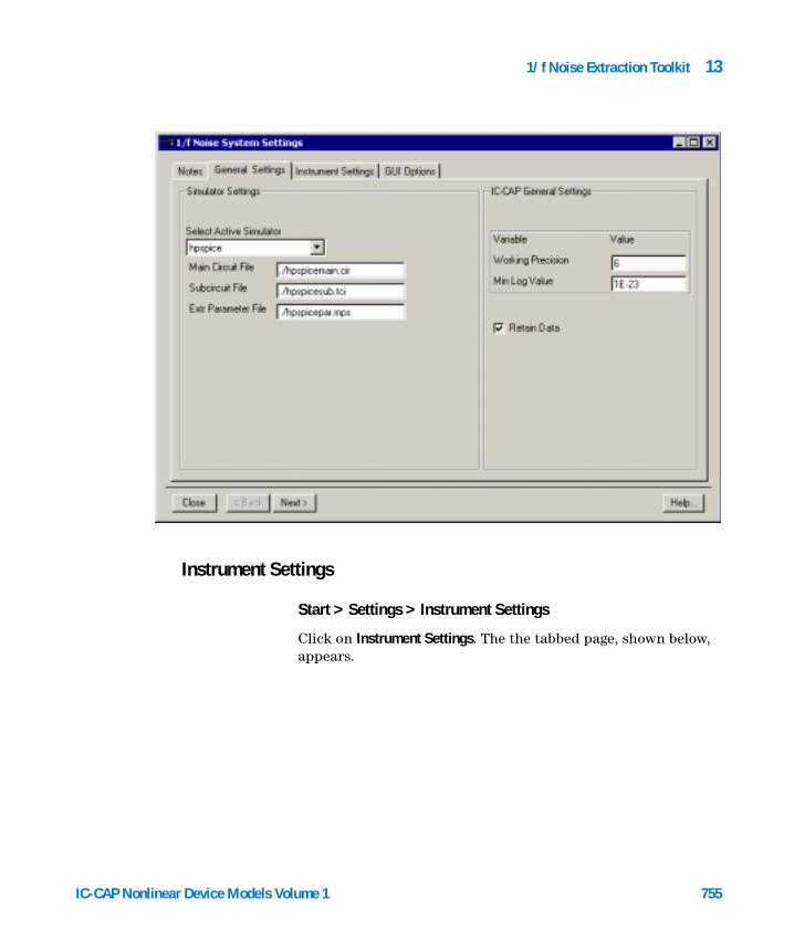
1/f Noise Extraction Toolkit 13
Instrument Settings
IC-CAP Nonlinear Device Models Vo
Start > Settings > Instrument Settings
Click on Instrument Settings. The the tabbed page, shown below, appears.
lume 1 755
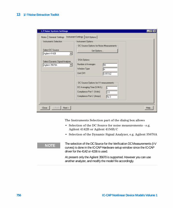
756
13 1/f Noise Extraction Toolkit
The Instruments Selection part of the dialog box allows
• Selection of the DC Source for noise measurements - e.g. Agilent 4142B or Agilent 4156B/C
• Selection of the Dynamic Signal Analyzer, e.g. Agilent 35670A
NOTE The selection of the DC Source for the Verification DC Measurements (I-V curves) is done in the IC-CAP Hardware setup window since the IC-CAP driver for the 4142 or 4156 is used.
At present only the Agilent 35670 is supported. However you can use another analyzer, and modify the model file accordingly.
IC-CAP Nonlinear Device Models Volume 1
1/f Noise Extraction Toolkit 13
IC-CAP Nonlinear Device Models Vo
The Instruments Options part of the dialog box allows
1 Setting DC Source Options for Noise Measurements by clicking on Set Options...
• Interface Name, e.g. lan[ ]:hpib, hpib, /dev/gpib0
• DC Source Address GP-IB address of the DC Source
• Unit Slot Number (For the 4142 or 4145, this is the actual slot of the SMU being used to bias the input of the device.)
• Force I/V For bipolar, current (I) is typically forced into the base. For MOS, voltage (V) is typically forced on the gate.
• Compliance Max voltage when forcing current (keep in mind the series resistance of the filter). Max current when forcing voltage.
These 5 settings (above) are used by the transforms NOISE_1f_force_ bias and NOISE_1f_stop_ bias to force the bias during noise measurements.
2 Setting DSA Options (These settings refer to the Agilent 35670 DSA)
• Number of Averages
• Window Type
• UnitCH1
3 Setting DC Source Options for I-V Measurements
The Toolkit uses the internal driver for the 3570 to measure the spectral noise density of the output noise. These settings will change the instrument options in the setup /Measure/Noise.
These settings are used by the 4142 or 4156 IC-CAP drivers to measure the I-V curves. See the Verify DC dialog.
• DC Averaging Time (S/M/L)
• Compliance Port 1
• Compliance Port 2
These settings will change the Instrument Option settings in the setup /Measure/DC-Sweep.
lume 1 757
13 1/f Noise Extraction Toolkit
GUI Options
758
Start > Settings > GUI Options
The General GUI Options part of the dialog box allows
• General GUI Options
• Activate check boxes for LNA settings
This option will display 3 check boxes - to be checked at each Noise Point measurement. The operation will go through each step of the settings each time checking the corresponding box. Only when all the boxes are checked will the measurement be allowed to proceed.
Plot Options
• Show Plots Automatically
• Annotate DC Plots
• Annotate Noise Plot
The Backup Options part of the dialog box allows
• Allow backup after measurements
• Ask after the measurement for backup
• Automatically backup setup Noise Data after measurements to mdm file: <filename>.
IC-CAP Nonlinear Device Models Volume 1

1/f Noise Extraction Toolkit 13
IC-CAP Nonlinear Device Models Volume 1 759
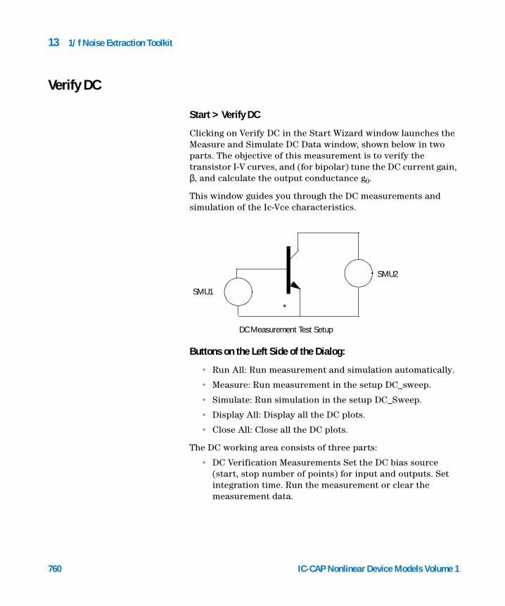
13 1/f Noise Extraction Toolkit
Verify DC
760
Start > Verify DC
Clicking on Verify DC in the Start Wizard window launches the Measure and Simulate DC Data window, shown below in two parts. The objective of this measurement is to verify the transistor I-V curves, and (for bipolar) tune the DC current gain, β, and calculate the output conductance g0.
This window guides you through the DC measurements and simulation of the Ic-Vce characteristics.
Buttons on the Left Side of the Dialog:
• Run All: Run measurement and simulation automatically.
• Measure: Run measurement in the setup DC_sweep.
• Simulate: Run simulation in the setup DC_Sweep.
• Display All: Display all the DC plots.
• Close All: Close all the DC plots.
The DC working area consists of three parts:
• DC Verification Measurements Set the DC bias source (start, stop number of points) for input and outputs. Set integration time. Run the measurement or clear the measurement data.
SMU1
SMU2
.
DC Measurement Test Setup
IC-CAP Nonlinear D
evice Models Volume 1
1/f Noise Extraction Toolkit 13
IC-CAP Nonlinear Device Models Vo
• Plots A text comment region lets you write text which will be reported in the output characteristics plot. Use Update Plot Annotation to update plot comments.The annotation macro is defined under Macros and is called dc_plot. Annotation will be printed with the plot. Also, any annotation text will be printed on the final report.
• Simulation Select the simulator. Use the Simulate button to run the simulation. The Tuning table allows you to fine tuning the device current gain β. This is extremely important since the device β will be used later in the final tuning of the extracted parameters obtained by comparing measured and simulated noise.
CAUTION Changing the simulator will load new Circuit, Subcircuit, and Parameter files (if those are found). Previous Circuit/Subcircuit and extracted parameters will be lost.
lume 1 761
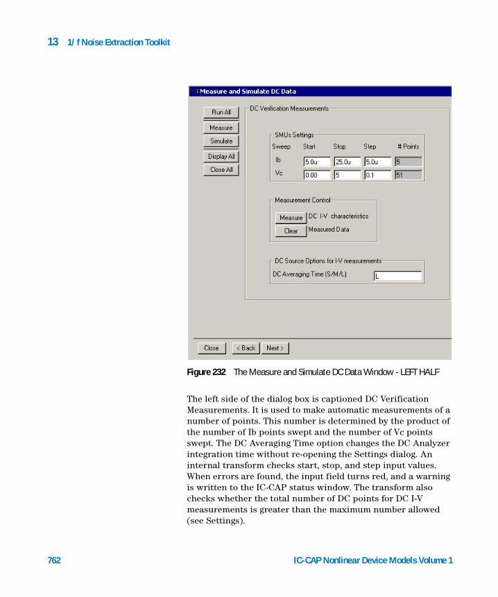
762
13 1/f Noise Extraction Toolkit
The left side of the dialog box is captioned DC Verification Measurements. It is used to make automatic measurements of a number of points. This number is determined by the product of the number of Ib points swept and the number of Vc points swept. The DC Averaging Time option changes the DC Analyzer integration time without re-opening the Settings dialog. An internal transform checks start, stop, and step input values. When errors are found, the input field turns red, and a warning is written to the IC-CAP status window. The transform also checks whether the total number of DC points for DC I-V measurements is greater than the maximum number allowed (see Settings).
Figure 232 The Measure and Simulate DC Data Window - LEFT HALF
IC-CAP Nonlinear Device Models Volume 1
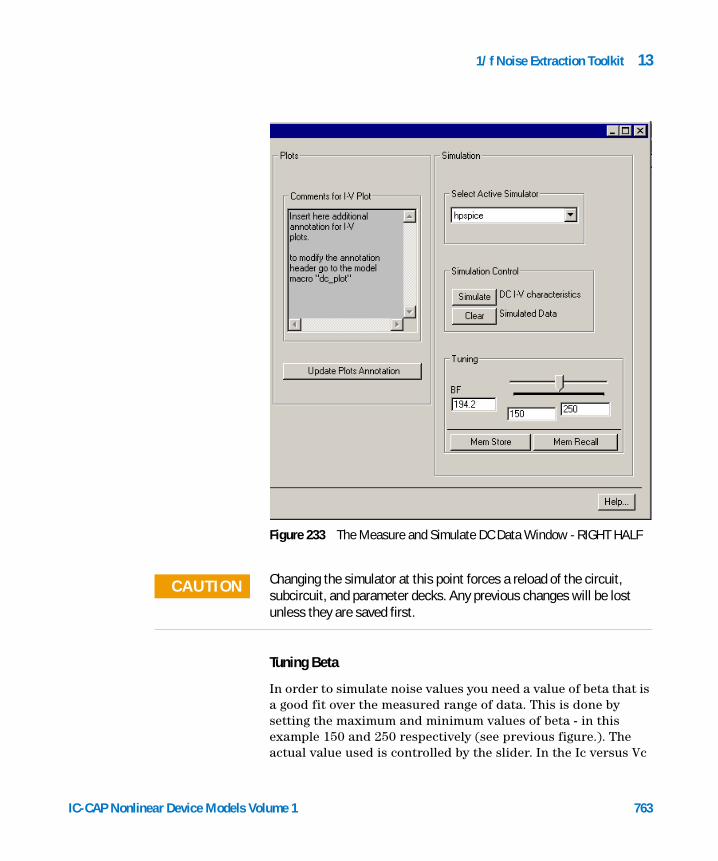
1/f Noise Extraction Toolkit 13
IC-CAP Nonlinear Device Models Vo
Figure 233 The Measure and Simulate DC Data Window - RIGHT HALF
CAUTION Changing the simulator at this point forces a reload of the circuit, subcircuit, and parameter decks. Any previous changes will be lost unless they are saved first.
Tuning Beta
In order to simulate noise values you need a value of beta that is a good fit over the measured range of data. This is done by setting the maximum and minimum values of beta - in this example 150 and 250 respectively (see previous figure.). The actual value used is controlled by the slider. In the Ic versus Vc
lume 1 763

764
13 1/f Noise Extraction Toolkit
plot (titled ic_vce), the yellow simulated (calculated) curves yellow match the red measured data curves best with beta (BF) at 150. See Figure below.
The Mem Store and Mem Recall buttons in the Tuning box allow you to store and recall the “tuned” values of beta for the subsequent noise measurements.
Plot NPN_1_f/measure/DC_Sweep/Ic_Vce (On)5mA max. DC offset of SR570
1/f Noise ToolkitDC Measurements and VerificationsDate: Wed July 18 12:52:44 PDT 2001-------------------------------------DC Bias Conditions:Ib Start: 5.0uIbStop: 25.0uIb Steps 5.0u
Vc Start: 0Vc Stop: 5
IC-CAP No
nlinear Device Models Volume 1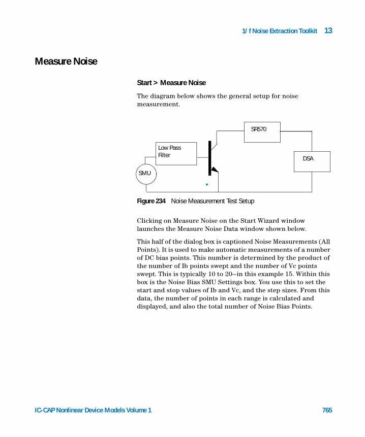
1/f Noise Extraction Toolkit 13
Measure Noise
IC-CAP Nonlinear Device Models Vo
Start > Measure Noise
The diagram below shows the general setup for noise measurement.
Clicking on Measure Noise on the Start Wizard window launches the Measure Noise Data window shown below.
This half of the dialog box is captioned Noise Measurements (All Points). It is used to make automatic measurements of a number of DC bias points. This number is determined by the product of the number of Ib points swept and the number of Vc points swept. This is typically 10 to 20—in this example 15. Within this box is the Noise Bias SMU Settings box. You use this to set the start and stop values of Ib and Vc, and the step sizes. From this data, the number of points in each range is calculated and displayed, and also the total number of Noise Bias Points.
Figure 234 Noise Measurement Test Setup
SMU
.
SR570
DSA
Low PassFilter
lume 1
765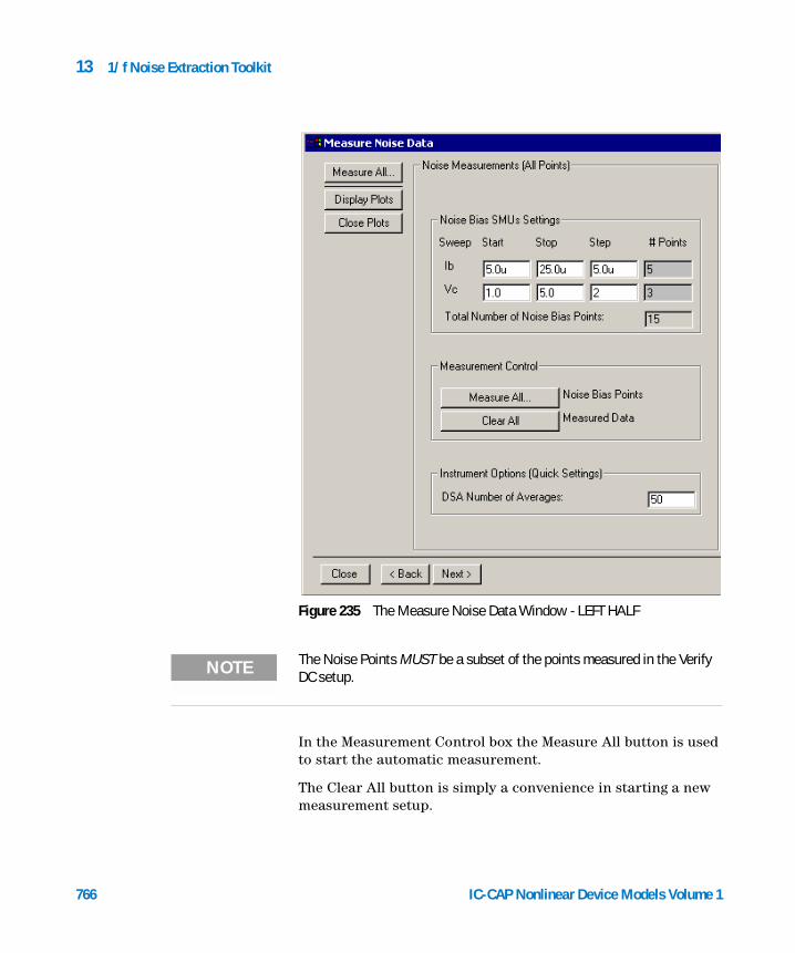
766
13 1/f Noise Extraction Toolkit
Figure 235 The Measure Noise Data Window - LEFT HALF
NOTE The Noise Points MUST be a subset of the points measured in the Verify DC setup.
In the Measurement Control box the Measure All button is used to start the automatic measurement.
The Clear All button is simply a convenience in starting a new measurement setup.
IC-CAP Nonlinear Device Models Volume 1
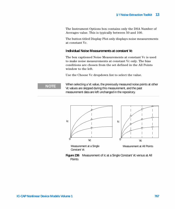
1/f Noise Extraction Toolkit 13
IC-CAP Nonlinear Device Models Vo
The Instrument Options box contains only the DSA Number of Averages value. This is typically between 50 and 100.
The button titled Display Plot only displays noise measurements at constant Vc.
Individual Noise Measurements at constant Vc
The box captioned Noise Measurements at constant Vc is used to make noise measurements at constant Vc only. The bias conditions are chosen from the set defined in the All Points window to the left.
Use the Choose Vc dropdown list to select the value.
NOTE When selecting a Vc value, the previously measured noise points at other Vc values are skipped during this measurement, and the past measurement data are left unchanged in the repository.
Figure 236 Measurement of Ic at a Single Constant Vc versus at AllPoints
Measurement at All Points
0
Ic
Vc
Ic
Vc
Measurement at a Single Constant Vc
0
lume 1
767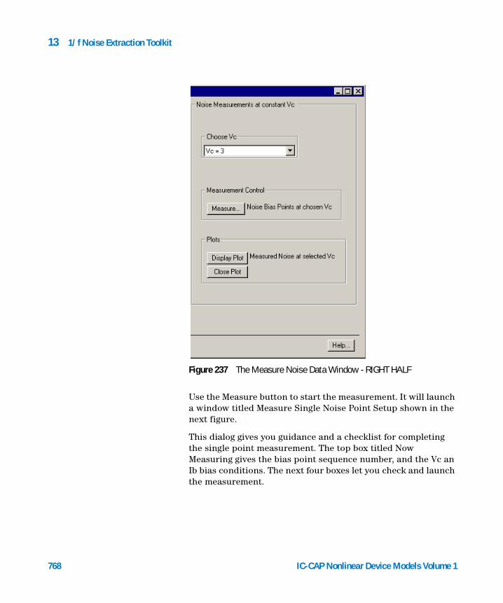
768
13 1/f Noise Extraction Toolkit
Use the Measure button to start the measurement. It will launch a window titled Measure Single Noise Point Setup shown in the next figure.
This dialog gives you guidance and a checklist for completing the single point measurement. The top box titled Now Measuring gives the bias point sequence number, and the Vc an Ib bias conditions. The next four boxes let you check and launch the measurement.
Figure 237 The Measure Noise Data Window - RIGHT HALF
IC-CAP Nonlinear Device Models Volume 1
1/f Noise Extraction Toolkit 13
NOTE Before launching the Single Measurement Point dialog, IC-CAP will automatically call the transform set_bias_force, which sets the Ib current into the base. At that point the input filter starts charging. Due to the low current level and the high RC constant, the charging can take as long as few minutes. In the meantime, user can proceed to step 1.
IC-CAP Nonlinear Device Models Vo
Step 1 Set the output bias voltage on the Low Noise Amplifier (LNA). In the Stanford Research LNA this has to be done manually. In the front panel, look under the area “Bias Voltage”. The output voltage is switched on using the “ON” button. The other buttons are used to set the voltage. The user should use a voltage multimeter to check the collector voltage by probing the contact labeled TEST. Check the check step 1 box when the LNA is set.
NOTE Before proceeding to the next step, make sure that the input filter has had enough time to be fully charged so that the device is biased at the chosen operating point.
Step 2 Set the current offset in the LNA. The suggested value is the value measured during the DC trace measurements for that bias point. For the Stanford Research LNA, this has to be done manually. Refer to the area labeled “Input Offset” in the LNA front panel. When set, check the check step 2 box. Choose a value as near as possible to the DC device output current.
Step 3 Set the sensitivity of the LNA. Refer to the area labeled “Sensitivity” in the LNA front panel. When in Demo mode, the suggested value of 4e−6 Amps/Volt is automatically generated and it is based on the device output conductance. In order to obtain the best performance out of the LNA, the sensitivity of the LNA should be set equal to the device output conductance. However, keep in mind the following considerations:
• The output conductance is calculated using a derivative function and therefore may be rather noisy and give non-meaningful values for the sensitivity.
• If the gain is too high, the amplifier output will saturate.
lume 1 769
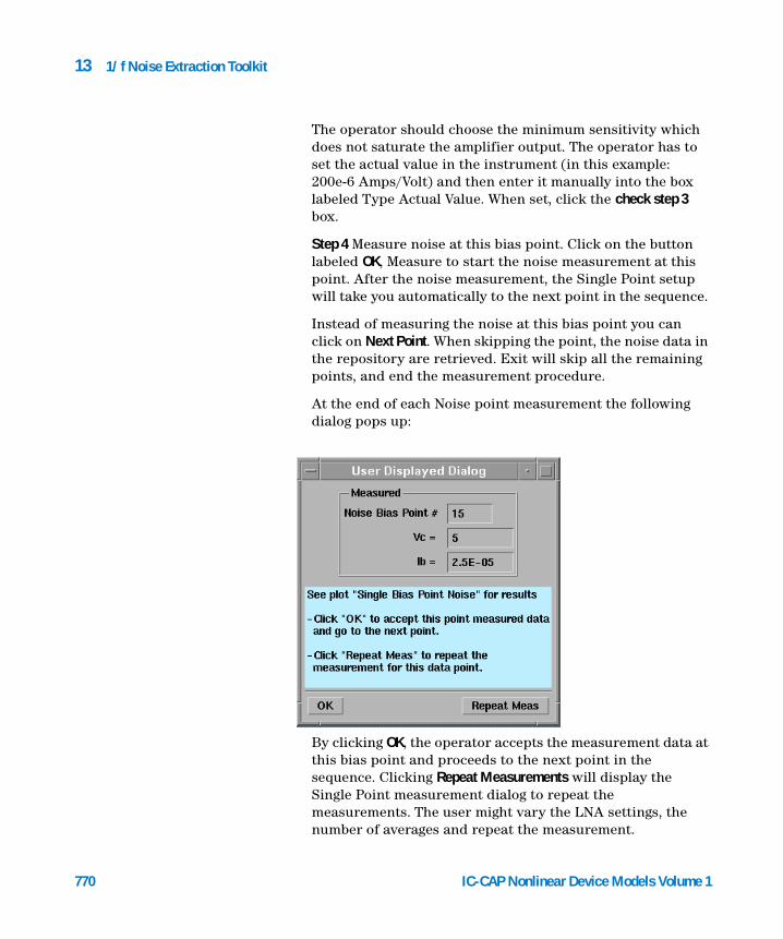
770
13 1/f Noise Extraction Toolkit
The operator should choose the minimum sensitivity which does not saturate the amplifier output. The operator has to set the actual value in the instrument (in this example: 200e-6 Amps/Volt) and then enter it manually into the box labeled Type Actual Value. When set, click the check step 3 box.
Step 4 Measure noise at this bias point. Click on the button labeled OK, Measure to start the noise measurement at this point. After the noise measurement, the Single Point setup will take you automatically to the next point in the sequence.
Instead of measuring the noise at this bias point you can click on Next Point. When skipping the point, the noise data in the repository are retrieved. Exit will skip all the remaining points, and end the measurement procedure.
At the end of each Noise point measurement the following dialog pops up:
By clicking OK, the operator accepts the measurement data at this bias point and proceeds to the next point in the sequence. Clicking Repeat Measurements will display the Single Point measurement dialog to repeat the measurements. The user might vary the LNA settings, the number of averages and repeat the measurement.
IC-CAP Nonlinear Device Models Volume 1
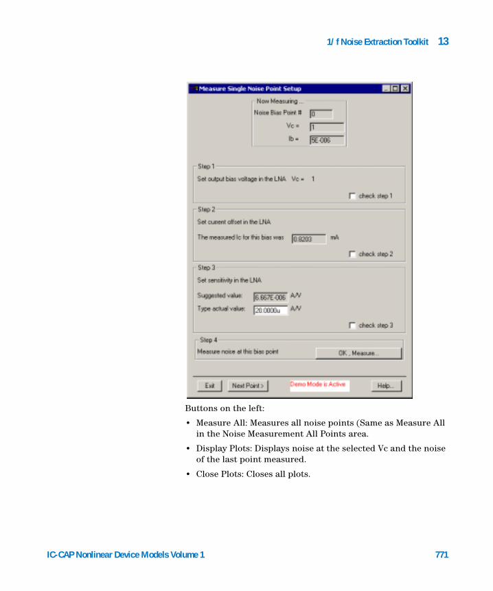
1/f Noise Extraction Toolkit 13
IC-CAP Nonlinear Device Models Vo
.
Buttons on the left:
• Measure All: Measures all noise points (Same as Measure All in the Noise Measurement All Points area.
• Display Plots: Displays noise at the selected Vc and the noise of the last point measured.
• Close Plots: Closes all plots.
lume 1 771
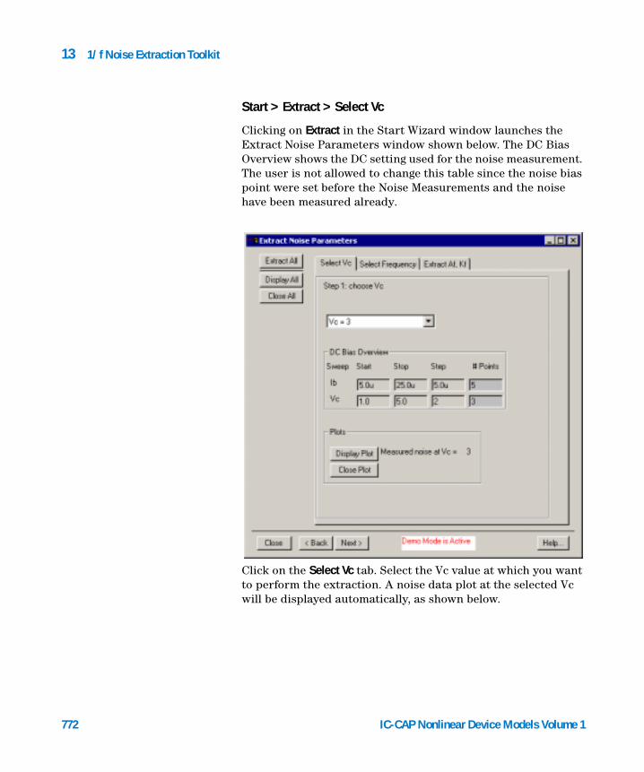
772
13 1/f Noise Extraction Toolkit
Start > Extract > Select Vc
Clicking on Extract in the Start Wizard window launches the Extract Noise Parameters window shown below. The DC Bias Overview shows the DC setting used for the noise measurement. The user is not allowed to change this table since the noise bias point were set before the Noise Measurements and the noise have been measured already.
Click on the Select Vc tab. Select the Vc value at which you want to perform the extraction. A noise data plot at the selected Vc will be displayed automatically, as shown below.
IC-CAP Nonlinear Device Models Volume 1
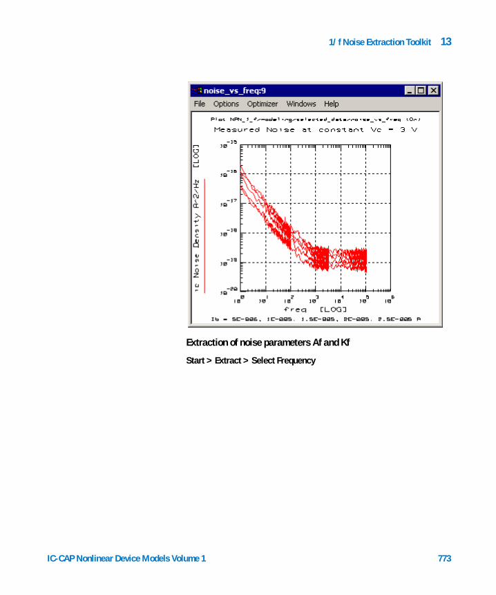
1/f Noise Extraction Toolkit 13
IC-CAP Nonlinear Device Models Vo
Extraction of noise parameters Af and Kf
Start > Extract > Select Frequency
lume 1 773
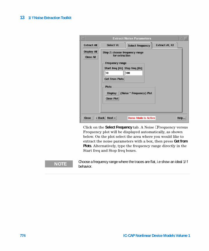
774
13 1/f Noise Extraction Toolkit
Click on the Select Frequency tab. A Noise ⋅ Frequency versus Frequency plot will be displayed automatically, as shown below. On the plot select the area where you would like to extract the noise parameters with a box, then press Get from Plots. Alternatively, type the frequency range directly in the Start freq and Stop freq boxes.
NOTE Choose a frequency range where the traces are flat, i.e show an ideal 1/f behavior.
IC-CAP Nonlinear Device Models Volume 1
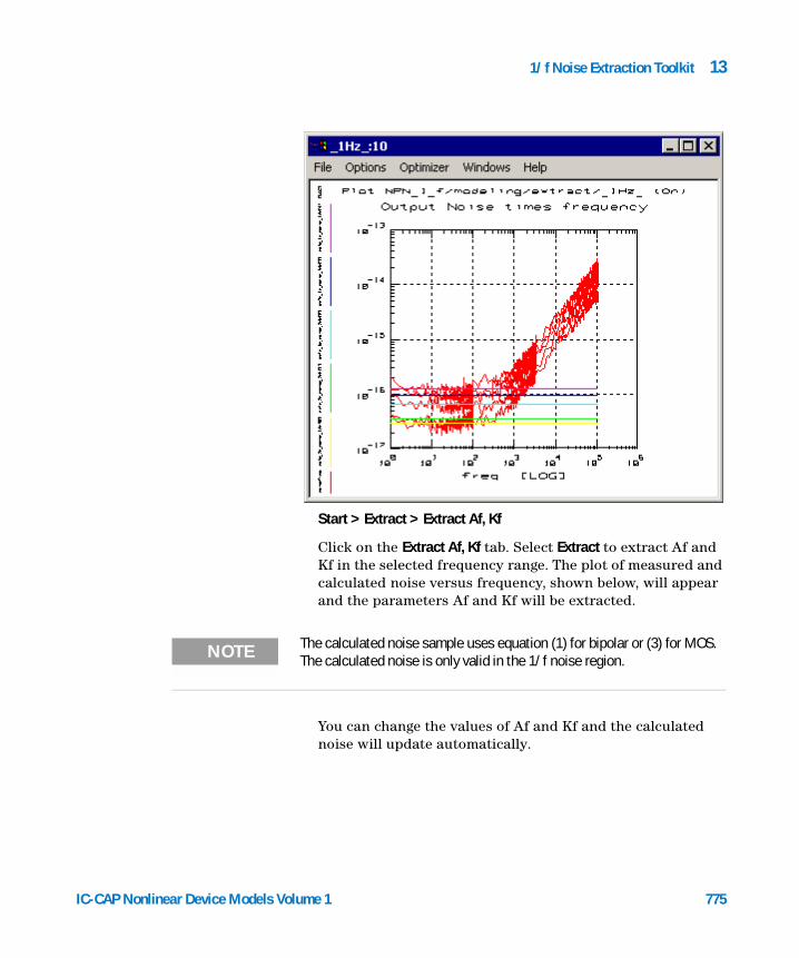
1/f Noise Extraction Toolkit 13
IC-CAP Nonlinear Device Models Vo
Start > Extract > Extract Af, Kf
Click on the Extract Af, Kf tab. Select Extract to extract Af and Kf in the selected frequency range. The plot of measured and calculated noise versus frequency, shown below, will appear and the parameters Af and Kf will be extracted.
NOTE The calculated noise sample uses equation (1) for bipolar or (3) for MOS. The calculated noise is only valid in the 1/f noise region.
You can change the values of Af and Kf and the calculated noise will update automatically.
lume 1 775
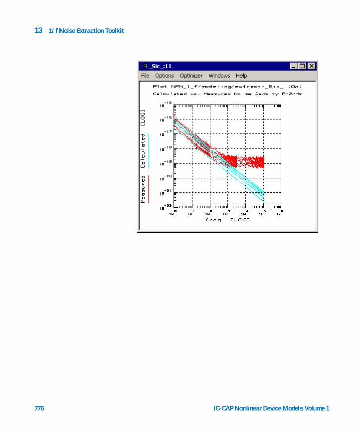
776
13 1/f Noise Extraction Toolkit
IC-CAP Nonlinear Device Models Volume 1

1/f Noise Extraction Toolkit 13
IC-CAP Nonlinear Device Models Vo
Buttons on Left Side of Dialog Box• Extract All: automatically extracts Af and Kf using the previously specified Vc and frequency range. Automatically opens all plots and ends in the last tab displaying the extracted Af and Kf.
• Display All: Displays all plots.
• Close All: Closes all plots.
Start > Simulate
Clicking on SImulate in the Start Wizard window launches the Simulate Noise window shown below.
lume 1 777
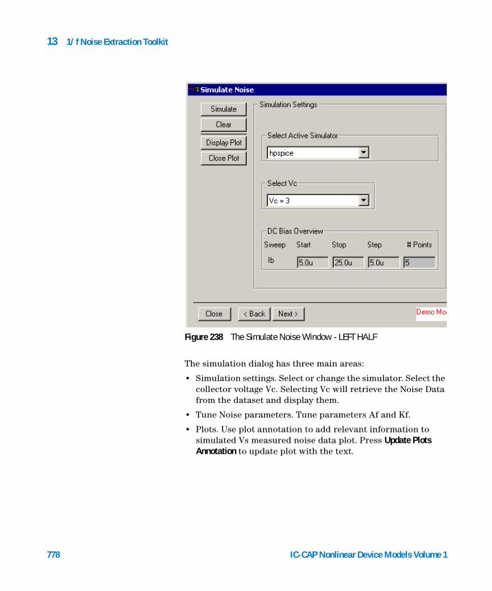
778
13 1/f Noise Extraction Toolkit
The simulation dialog has three main areas:
• Simulation settings. Select or change the simulator. Select the collector voltage Vc. Selecting Vc will retrieve the Noise Data from the dataset and display them.
• Tune Noise parameters. Tune parameters Af and Kf.
• Plots. Use plot annotation to add relevant information to simulated Vs measured noise data plot. Press Update Plots Annotation to update plot with the text.
Figure 238 The Simulate Noise Window - LEFT HALF
IC-CAP Nonlinear Device Models Volume 1
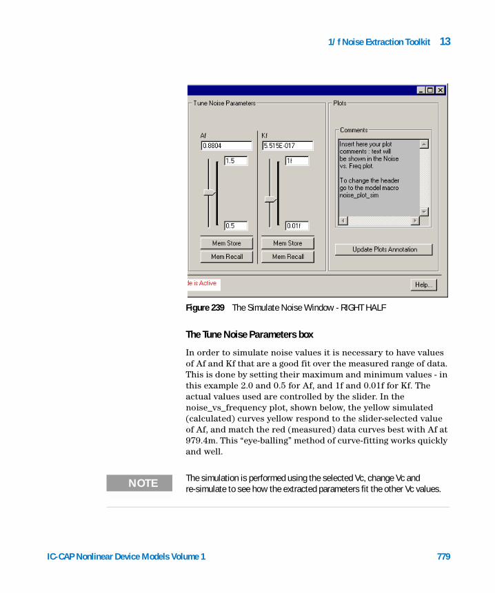
1/f Noise Extraction Toolkit 13
IC-CAP Nonlinear Device Models Vo
The Tune Noise Parameters box
In order to simulate noise values it is necessary to have values of Af and Kf that are a good fit over the measured range of data. This is done by setting their maximum and minimum values - in this example 2.0 and 0.5 for Af, and 1f and 0.01f for Kf. The actual values used are controlled by the slider. In the noise_vs_frequency plot, shown below, the yellow simulated (calculated) curves yellow respond to the slider-selected value of Af, and match the red (measured) data curves best with Af at 979.4m. This “eye-balling” method of curve-fitting works quickly and well.
Figure 239 The Simulate Noise Window - RIGHT HALF
NOTE The simulation is performed using the selected Vc, change Vc and re-simulate to see how the extracted parameters fit the other Vc values.
lume 1 779

13 1/f Noise Extraction Toolkit
780
Buttons on the Left Side of the Dialog:
Simulate: runs simulation in setup verify/simulate.
Clear: clears simulated data.
Display Plots: displays measured vs simulated noise data at constant Vc.
Close Plots: closes noise plot.
Start > Data Manager
Clicking on Data Manager in the Start Wizard window launches the Data Manager Dialog window shown below.
IC-CAP Nonlinear Device Models Volume 1
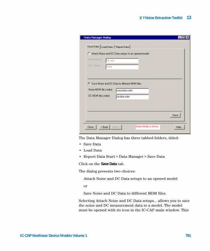
1/f Noise Extraction Toolkit 13
IC-CAP Nonlinear Device Models Vo
The Data Manager Dialog has three tabbed folders, titled:
• Save Data
• Load Data
• Report Data Start > Data Manager > Save Data
Click on the Save Data tab.
The dialog presents two choices:
Attach Noise and DC Data setups to an opened model
or
Save Noise and DC Data to different MDM files.
Selecting Attach Noise and DC Data setups... allows you to save the noise and DC measurement data to a model. The model must be opened with its icon in the IC-CAP main window. This
lume 1 781
782
13 1/f Noise Extraction Toolkit
option may be useful when you want to keep all the measurement data (electrical, noise, etc.) in the same model file.
Selecting Save Noise and DC Data to different MDM files Noise and DC data are saved in the specified MDM files.
Important Note: Along with the DC and Noise Data, IC-CAP also saves to a DUT or the MDM files some key setting variables and the extracted noise parameters. IC-CAP saves the following variables:
• the DC sweeps variables (inDC_IB_START, inDC_IB_STOP, inDC_IB_STEP, inDC_VCE_START, etc.) and the extracted BF.
• the noise sweep variables (inNOISE_IB_START, inNOISE_IB_STOP, etc.).
• the extracted noise parameters Af, Kf (Ef for CMOS).
• the sensitivity settings of the LNA (Sensitivity). This is essential to display the noise when reading the files back.
Start > Data Manager > Load Data
Click on the Load Data folder.
Select Read Noise and DC Data from an opened model to read noise and DC measurement data from a model. The model must be opened and located in the IC-CAP main window. Selecting Read reads DC and Noise measurement data from the DUT to the repository’s setups.
DC_Sweep and Noise Data.
CAUTION Bias settings for DC and Noise measurements will be changed according to the settings stored in the DUT. Actual DC and Noise bias settings, extracted values, and LNA sensitivity settings will be lost and replaced by the values saved in the DUT.
Select Read Noise and DC Data from MDM files to save Noise and DC data to the specified MDM files.
IC-CAP Nonlinear Device Models Volume 1
1/f Noise Extraction Toolkit 13
CAUTION Bias settings for DC and Noise measurements will be changed according to the settings in the MDM files. Actual DC and Noise bias settings, extracted values and LNA sensitivity settings will be lost and replaced by the values saved in the MDM files.
IC-CAP Nonlinear Device Models Vo
Start > Data Manager > Report Data
Report Data tab folder.
Select Generate Report to write a text report to the specified file name. To change the report format see transform Gui Driver/Data Manager/Generate Text.
lume 1 783
13 1/f Noise Extraction Toolkit
1/f Noise Extraction with MOS Transistors
784
All previous examples in this chapter have dealt with bipolar junction transistors.
The model selected was .../examples/model_files/noise/1_f_toolkit/bjt_1f_noise.mdl.3For MOS transistors use this model instead.../examples/model_files/noise/1_f_toolkit/mos_1f_noise.mdl.
The basic operation for MOS is the same as for bipolar, except where shown in this section.
Some Basic Differences
Terminals The emitter, base and collector terminal are replaced by the source, gate and drain terminals respectively.
Impedances The bipolar transistor has a low input impedance from base to emitter, whereas the gate to source impedance of the MOS transistor is essentially infinite.
Currents The drain current Ids replaces the collector current Ice.
Voltages The voltages Ib and Vce are replaced by Vgs and Vds respectively, as shown in the Measure and Simulate DC Data Dialog Box show below.
IC-CAP Nonlinear Device Models Volume 1
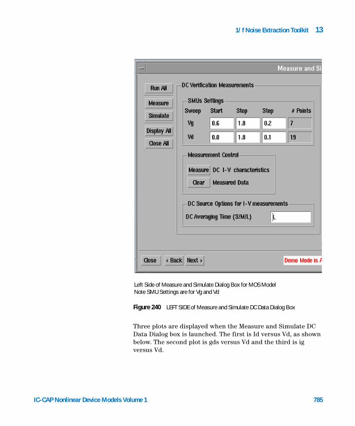
1/f Noise Extraction Toolkit 13
IC-CAP Nonlinear Device Models Vo
Three plots are displayed when the Measure and Simulate DC Data Dialog box is launched. The first is Id versus Vd, as shown below. The second plot is gds versus Vd and the third is ig versus Vd.Figure 240 LEFT SIDE of Measure and Simulate DC Data Dialog Box
Left Side of Measure and Simulate Dialog Box for MOS ModelNote SMU Settings are for Vg and Vd
lume 1 785
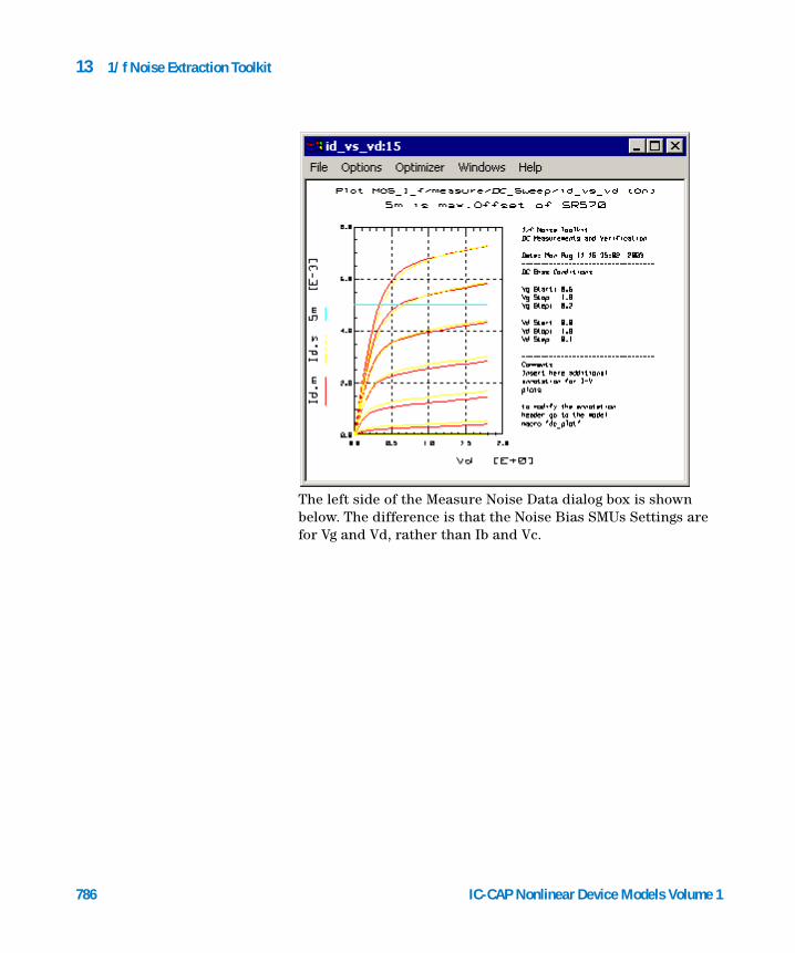
786
13 1/f Noise Extraction Toolkit
The left side of the Measure Noise Data dialog box is shown below. The difference is that the Noise Bias SMUs Settings are for Vg and Vd, rather than Ib and Vc.
IC-CAP Nonlinear Device Models Volume 1
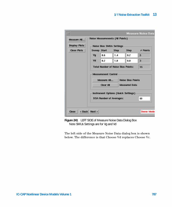
1/f Noise Extraction Toolkit 13
IC-CAP Nonlinear Device Models Vo
The left side of the Measure Noise Data dialog box is shown below. The difference is that Choose Vd replaces Choose Vc.
Figure 241 LEFT SIDE of Measure Noise Data Dialog BoxNote SMUs Settings are for Vg and Vd
lume 1 787
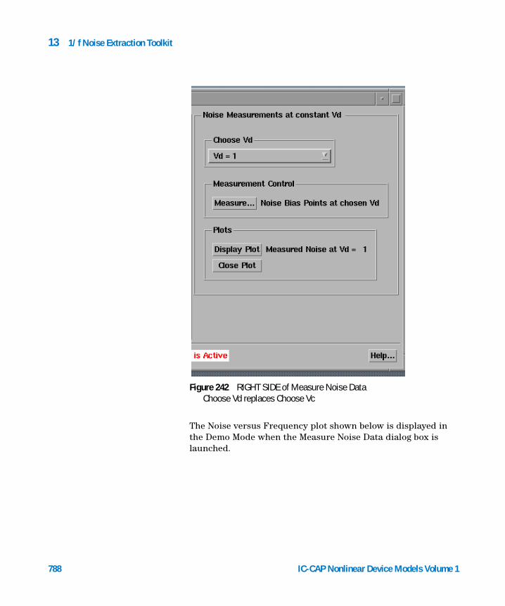
788
13 1/f Noise Extraction Toolkit
The Noise versus Frequency plot shown below is displayed in the Demo Mode when the Measure Noise Data dialog box is launched.
Figure 242 RIGHT SIDE of Measure Noise DataChoose Vd replaces Choose Vc
IC-CAP Nonlinear Device Models Volume 1
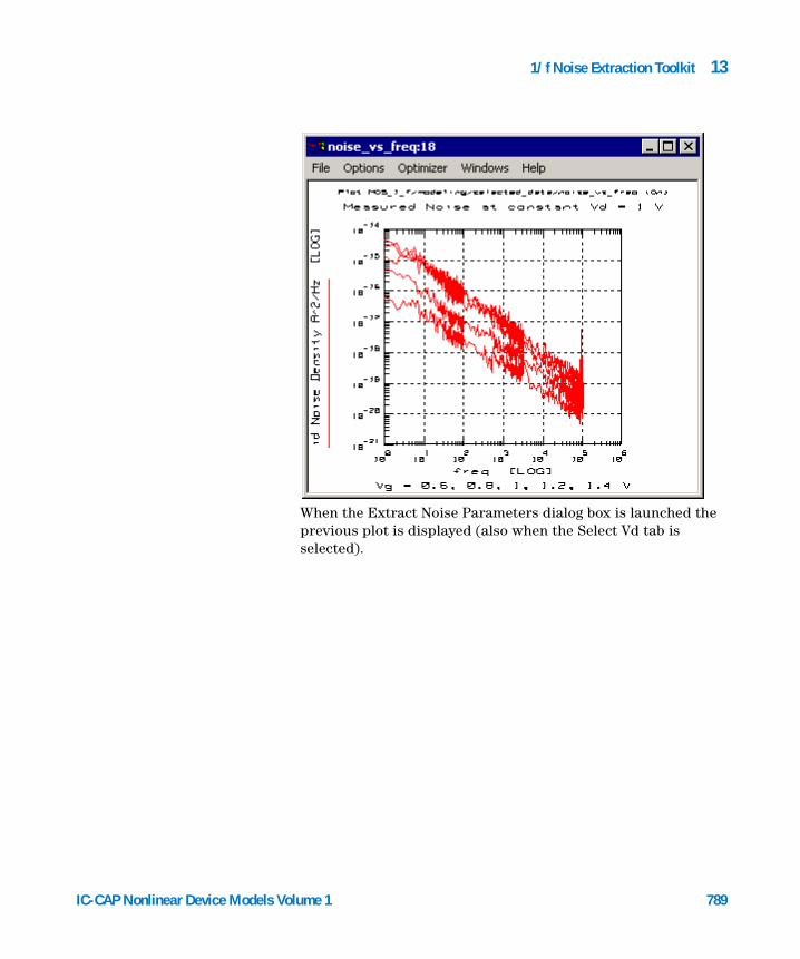
1/f Noise Extraction Toolkit 13
IC-CAP Nonlinear Device Models Vo
When the Extract Noise Parameters dialog box is launched the previous plot is displayed (also when the Select Vd tab is selected).
lume 1 789
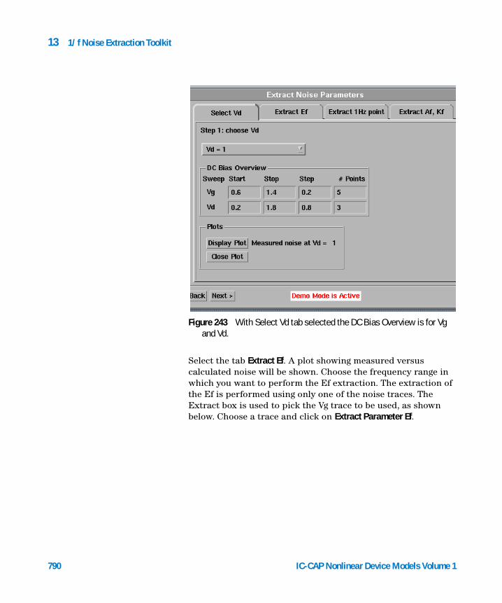
790
13 1/f Noise Extraction Toolkit
Select the tab Extract Ef. A plot showing measured versus calculated noise will be shown. Choose the frequency range in which you want to perform the Ef extraction. The extraction of the Ef is performed using only one of the noise traces. The Extract box is used to pick the Vg trace to be used, as shown below. Choose a trace and click on Extract Parameter Ef.
Figure 243 With Select Vd tab selected the DC Bias Overview is for Vg and Vd.
IC-CAP Nonlinear Device Models Volume 1
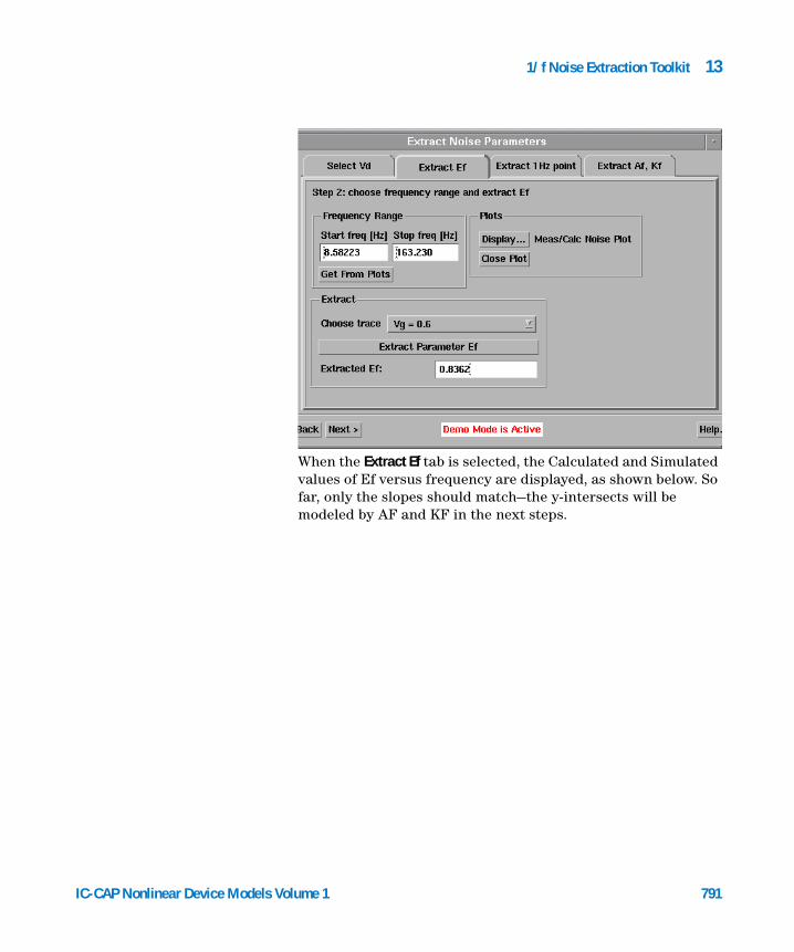
1/f Noise Extraction Toolkit 13
IC-CAP Nonlinear Device Models Vo
When the Extract Ef tab is selected, the Calculated and Simulated values of Ef versus frequency are displayed, as shown below. So far, only the slopes should match—the y-intersects will be modeled by AF and KF in the next steps.
lume 1 791
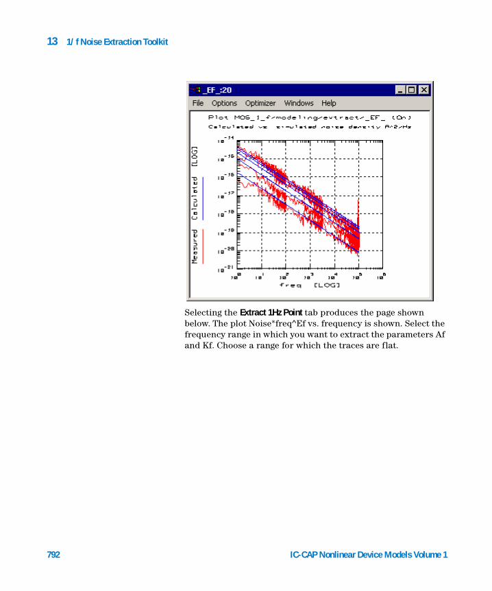
792
13 1/f Noise Extraction Toolkit
Selecting the Extract 1Hz Point tab produces the page shown below. The plot Noise*freq^Ef vs. frequency is shown. Select the frequency range in which you want to extract the parameters Af and Kf. Choose a range for which the traces are flat.
IC-CAP Nonlinear Device Models Volume 1
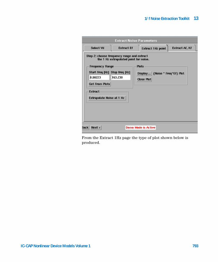
1/f Noise Extraction Toolkit 13
IC-CAP Nonlinear Device Models Vo
From the Extract 1Hz page the type of plot shown below is produced.
lume 1 793
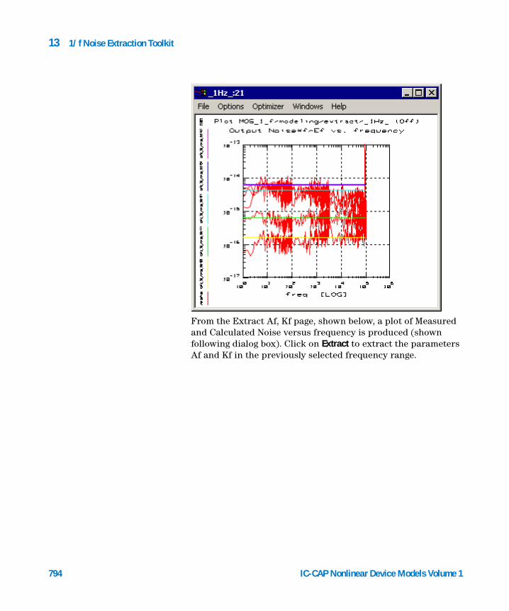
794
13 1/f Noise Extraction Toolkit
From the Extract Af, Kf page, shown below, a plot of Measured and Calculated Noise versus frequency is produced (shown following dialog box). Click on Extract to extract the parameters Af and Kf in the previously selected frequency range.
IC-CAP Nonlinear Device Models Volume 1
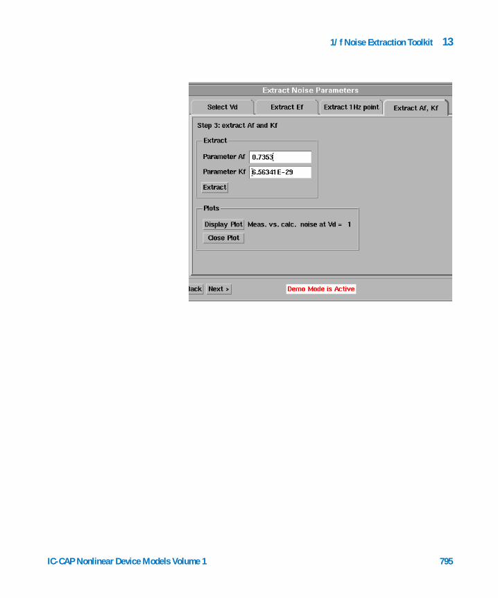
1/f Noise Extraction Toolkit 13
IC-CAP Nonlinear Device Models Vo
lume 1 795

796
13 1/f Noise Extraction Toolkit
From the Simulate Noise dialog box a plot of Measured and Simulated Noise versus frequency is produced, as shown below.
IC-CAP Nonlinear Device Models Volume 1
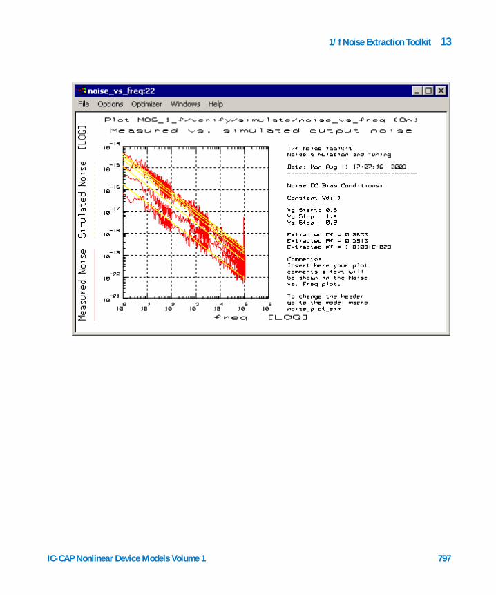
1/f Noise Extraction Toolkit 13
IC-CAP Nonlinear Device Models Volume 1 797

13 1/f Noise Extraction Toolkit
1/f Noise Function Descriptions
798
Function Name Function Description
Noise_1f_bjt_1Hz For each noise trace this function finds the 1 Hz intercept point by calculating the average noise in the specified frequency range. The frequency range can be specified by using the variables X_LOW and X_HIGH. If N is the number of noise traces, the function returns an output dataset of size N filled with the N intercept points (one for each trace).
Noise_1f_bjt_calc This function calculates the current noise density at the device output (collector) given the frequency range, the device current gain Bf, the base current and the parameters Af and Kf listed in the Parameters table. The noise is calculated as follows:<Sic>= Kf * (ib^Af)/f * Beta^2If N is the number of traces (number of DC bias points) the inputs are defined as follows:Inputs:Beta: Dc current gain dataset. Size: Nfrequency: Frequency point dataset.Size: N*freqpoints.Base Current: Base current dataset. Size: N.Output:Dataset filled with the calculated noise.Size: N*freqpoints.Examples:This transform is used during 1/f noise parameters extraction for bipolar devices. See model fileexamples/model_files/noise/1_f_toolkit/bjt_1f_noise.mdl The transform is used in the setup modeling/extract.
Noise_1f_bjt_extract This function extracts the parameters Af and Kf. If N is the number of noise traces at a given Vc, inputs and output are as follows:Inputs:Beta: Dc current gain dataset. Size: N.Ic noise 1 Hz: 1 Hz intercept dataset. Size: N.Base Current: base current at each bias point. Size: N.Output:Return a dataset of size N with the calculated 1 Hz values using the extracted Af and Kf.Examples:This transform is used during 1/f noise parameters extraction for bipolar devices. See model file examples/model_files/noise/1_f_toolkit/bjt_1f_noise.mdl The transform is used in the setup modeling/extract.
IC-CAP Nonlinear Device Models Volume 1
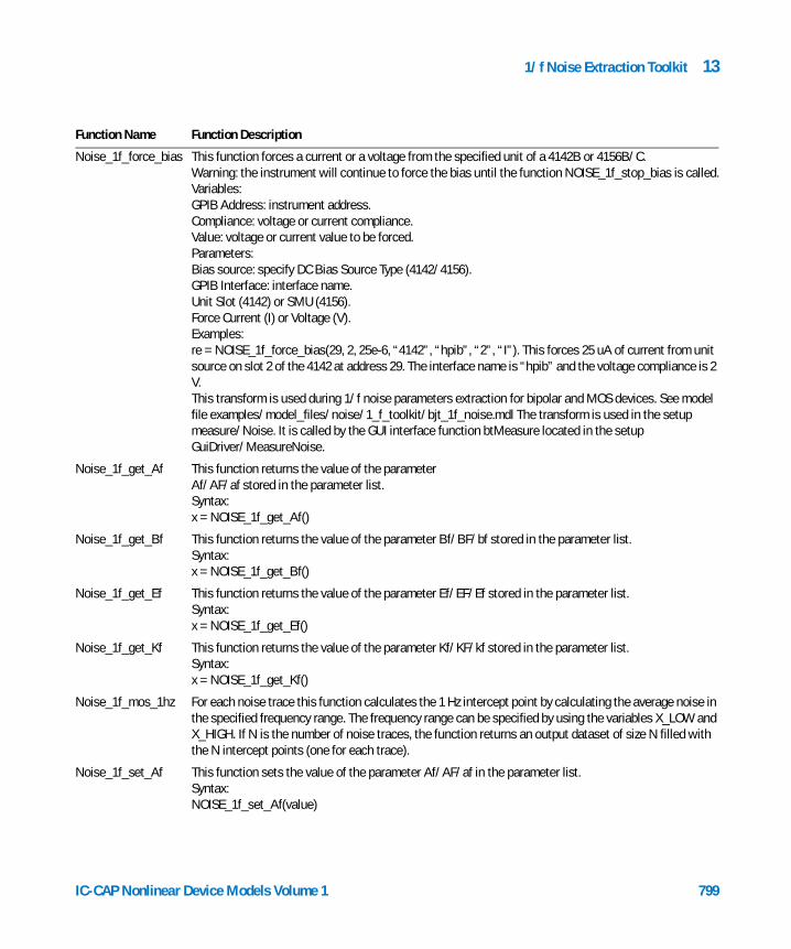
1/f Noise Extraction Toolkit 13
Noise_1f_force_bias This function forces a current or a voltage from the specified unit of a 4142B or 4156B/C. Warning: the instrument will continue to force the bias until the function NOISE_1f_stop_bias is called.Variables:GPIB Address: instrument address.Compliance: voltage or current compliance.Value: voltage or current value to be forced. Parameters:Bias source: specify DC Bias Source Type (4142/4156).GPIB Interface: interface name.Unit Slot (4142) or SMU (4156).Force Current (I) or Voltage (V).Examples:re = NOISE_1f_force_bias(29, 2, 25e-6, “4142”, “hpib”, “2”, “I”). This forces 25 uA of current from unit source on slot 2 of the 4142 at address 29. The interface name is “hpib” and the voltage compliance is 2 V.This transform is used during 1/f noise parameters extraction for bipolar and MOS devices. See model file examples/model_files/noise/1_f_toolkit/bjt_1f_noise.mdl The transform is used in the setup measure/Noise. It is called by the GUI interface function btMeasure located in the setup GuiDriver/MeasureNoise.
Noise_1f_get_Af This function returns the value of the parameterAf/AF/af stored in the parameter list.Syntax:x = NOISE_1f_get_Af()
Noise_1f_get_Bf This function returns the value of the parameter Bf/BF/bf stored in the parameter list.Syntax:x = NOISE_1f_get_Bf()
Noise_1f_get_Ef This function returns the value of the parameter Ef/EF/Ef stored in the parameter list.Syntax:x = NOISE_1f_get_Ef()
Noise_1f_get_Kf This function returns the value of the parameter Kf/KF/kf stored in the parameter list.Syntax:x = NOISE_1f_get_Kf()
Noise_1f_mos_1hz For each noise trace this function calculates the 1 Hz intercept point by calculating the average noise in the specified frequency range. The frequency range can be specified by using the variables X_LOW and X_HIGH. If N is the number of noise traces, the function returns an output dataset of size N filled with the N intercept points (one for each trace).
Noise_1f_set_Af This function sets the value of the parameter Af/AF/af in the parameter list.Syntax:NOISE_1f_set_Af(value)
Function Name Function Description
IC-CAP Nonlinear Device Models Volume 1 799
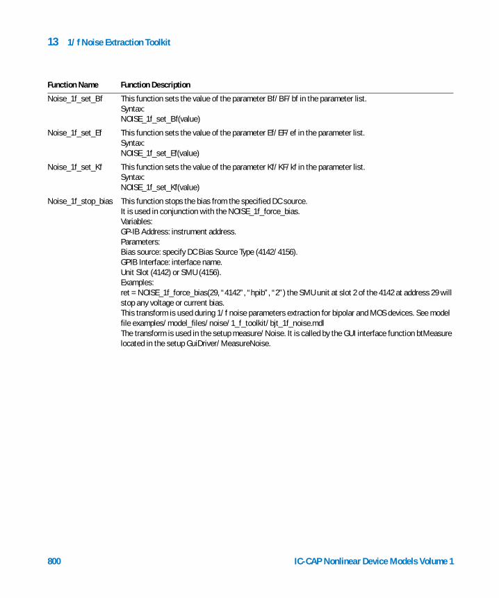
13 1/f Noise Extraction Toolkit
Noise_1f_set_Bf This function sets the value of the parameter Bf/BF/bf in the parameter list.Syntax:NOISE_1f_set_Bf(value)
Noise_1f_set_Ef This function sets the value of the parameter Ef/EF/ef in the parameter list.Syntax:NOISE_1f_set_Ef(value)
Noise_1f_set_Kf This function sets the value of the parameter Kf/KF/kf in the parameter list.Syntax:NOISE_1f_set_Kf(value)
Noise_1f_stop_bias This function stops the bias from the specified DC source.It is used in conjunction with the NOISE_1f_force_bias.Variables:GP-IB Address: instrument address.Parameters:Bias source: specify DC Bias Source Type (4142/4156).GPIB Interface: interface name.Unit Slot (4142) or SMU (4156).Examples:ret = NOISE_1f_force_bias(29, “4142”, “hpib”, “2”) the SMU unit at slot 2 of the 4142 at address 29 will stop any voltage or current bias.This transform is used during 1/f noise parameters extraction for bipolar and MOS devices. See model file examples/model_files/noise/1_f_toolkit/bjt_1f_noise.mdlThe transform is used in the setup measure/Noise. It is called by the GUI interface function btMeasure located in the setup GuiDriver/MeasureNoise.
Function Name Function Description
800 IC-CAP Nonlinear Device Models Volume 1

1/f Noise Extraction Toolkit 13
References
IC-CAP Nonlinear Device Models Vo
1 “Simulating Noise in Nonlinear Circuits Using the HP Microwave and Design System”. Agilent Product Note 85150-4,1993. http://www.agilent.com
2 IC-CAP Noise Modeling Workshop. Agilent Technologies, Germany and Technical University of Munich, Institute of High Frequency Techniques. Munich, Germany 1998.
3 F. X. Sinnesbichler, M. Fisher, G. R. Olbrich, “Accurate Extraction Method for 1/f Noise Parameters
4 Used in G-P Type Bipolar Junction Transistor Models”. IEEE MTT-S Symposium, Baltimore, 1998.
5 C. G. Jakobson, I. Bloom, Y. Nemirovsky. “1/f Noise in CMOS Transistors for Analog Applications”. 19. Convention of Electrical and Electronics Engineers in Israel, 1996. pp. 557-560.
6 Private communication: G. Knoblinger, Infineon AG, Munich and F. Sischka.
7 A. Blaum, O. Pilloud, G. Scalea, J. Victory, F. Sischka. “A New Robust On-Wafer 1/f Noise Measurement and Characterization System”. To be published: ICMTS Conference 2001, Kobe, Japan.
8 Stanford Research SR570 Low-Noise Current Preamplifier.
See http://www.srsys.com
9 A. Van Der Ziel. “Noise, Sources, Characterization, Measurement”, Prentice Hall, 1970.
lume 1 801

802
13 1/f Noise Extraction Toolkit
IC-CAP Nonlinear Device Models Volume 1
Index
Numerics1/f Noise
Af, 775Af MOS, 794beta tuning, 763data manager, 780Ef MOS, 790extract Af, Kf, 775extract noise parameters, 772function descriptions, 798general settings, 754GUI options, 758hardware, 748Id/Vd curves, 785individual noise measurements, 767instrument settings, 755Kf, 775Kf MOS, 794measure noise, 765modeling, 740MOS transistors, 784notes, 752references, 801simulate, 777software, 748system settings, 752test setup, 765tune noise parameters, 779verify DC, 760
AAC extraction, 584Af MOS, 794Agilent-HBT model, 587
IC-CAP Nonlinear Device Models Vo
AHBTCJ extraction, 656data ranges, 636DC extraction, 647DC measurements, 609de-embedding pad parasitics, 618displaying plots, 642exporting/importing data, 621extraction options, 645extraction overview, 647extraction/optimization, 629FT extraction, 656function execution, 632instrument settings, 599key features, 589measurement options, 620measurement settings, 603pad open/short measurements, 605parameter boundaries, 627R extraction, 655requirements, 589RF measurements, 615simulation, 625SP extraction, 656
AHBT_Package.mdl, 590algorithms
bipolar transistor, 582MOSFET, 553
alternative extractionCurtice GaAs MESFET, 701UCB GaAs MESFET, 676
Bbeta tuning, 763
lume 1
bipolar transistorAC extraction, 584algorithms, 582characterization, 561connections, 571cv extraction, 583DC extraction, 582extracting parameters, 577extraction guidelines, 573instrument options, 573instruments, 571measurement hints, 574model, 563NPN, 561optimizing, 576parameters, 565PNP, 577resistance extraction, 583, 584simulating, 564, 575
bjt_1f_noise.mdl, 749bjt_npn.mdl, 561bjt_pnp.mdl, 561BSIM4
Acknowledgements, 320Capacitance, 55Data Structure inside the BSIM4
Modeling Package, 18DC Diode, 62DC Transistor, 33DC Transistor DUT’s, 40Drain/Source – Bulk Diodes for DC
Measurements, 65finetuning, BSIM, 111Measurement, 23Measurement Conditions, 30Options, 65Project Notes, 26Switch Matrix, 27Temperature Setup, 26Teststructures for Deep Submicron
CMOS Processes, 297
803
Index
Ccalibration, MOSFET, 543capacitance extraction
Curtice GaAs MESFET, 699UCB GaAs MESFET, 675
CGaas1.mdl, 683CGaas2.mdl, 683characterization circuits, 707circuits
characterizing, 707characterizing portions, 713defining, 710design optimization, 719ECL OR/NOR logic gate, 711extracting parameters, 715measurement, 713modeling, 707multiple instruments, 713NPN with PNP, 725operational amplifier, 727optimizing parameters, 716simulation, 719test, 721types, 725
connectionsbipolar transistor, 571MOSFET, 541
804
Curtice GaAs MESFETalternative extraction method, 701capacitance parameter extraction, 699,
705DC extraction, 704device connections, 692diode parameter extraction, 699extraction algorithms, 704extraction guidelines, 694extraction procedure, 698extraction procedure overview, 697inductance extraction, 704inductance parameter extraction, 699instrument calibration, 695instrument options, 694linear parameter extraction, 699measuring instruments, 695model, 685N-channel, 687optimizing, 697, 703P-channel, 687resistance extraction, 704resistance parameter extraction, 699saturation parameter extraction, 699simulating, 696, 703simulators, 686transistor, 683
cv extractionbipolar transistor, 583MOSFET, 549, 554
Ddata manager, 780DC extraction
AHBT, 647bipolar transistor, 582Curtice GaAs MESFET, 704MOSFET, 546, 553UCB GaAs MESFET, 680
DC Transistor, 33design optimization circuits, 719device connections, 692diode parameter extraction, 699dutx, 496
EECL OR/NOR logic gate, 711
IC-CAP
Ef MOS, 790example files
AHBT_Package.mdl, 590bjt_1f_noise.mdl, 749bjt_npn.mdl, 561bjt_pnp.mdl, 561CGaas1.mdl, 683CGaas2.mdl, 683hnmos6.mdl, 556nmos2.mdl, 532nmos3.mdl, 532npnwpnp.mdl, 583, 726opamp.mdl, 728pmos2.mdl, 532pmos3.mdl, 532UCBGaas.mdl, 663
extractAf, 775Af, Kf, 775Kf, 775MM9 DUTs, 484noise parameters, 772
extracting parametersAHBT, 625bipolar transistor, 577circuits, 715MOSFET, 545PSP, 197
extractionalgorithms
Curtice GaAs MESFET, 704UCB GaAs MESFET, 680
bipolar transistor, 573guidelines
Curtice GaAs MESFET, 694UCB GaAs MESFET, 670
HSPICE level 6, 559MOSFET, 543procedure
Curtice GaAs MESFET, 697MESFET, 673
UCB GaAs MESFET, 674
Ffinetune, 111function descriptions, 798
Nonlinear Device Models Volume 1
Index
Ggeometry, single, 549GUI options, 758
HHBT device modeling, 587hierarchy test circuit, 723hnmos6.mdl, 556HSPICE
Level 6 MOSFET model, 556
IId/Vd curves, 785Import measured data, 66inductance extraction
Curtice GaAs MESFET, 704UCB GaAs MESFET, 680
instrumentcalibration
Curtice GaAs MESFET, 695UCB GaAs MESFET, 671
optionsbipolar transistor, 573Curtice GaAs MESFET, 694MOSFET, 543
settings1/f Noise, 755UCB GaAs MESFET, 670
instrumentsbipolar transistor, 571MOSFET, 541, 543multiple, 713UCB GaAs MESFET, 669
JJUNCAP model, 513
KKf MOS, 794
Llinear parameter extraction, 699
IC-CAP Nonlinear Device Models Vo
Mmacro modeling, 707macros, MM9, 501measurement circuit, 713measurement of the devices, 49measuring instruments
Curtice GaAs MESFET, 695UCB GaAs MESFET, 671
MESFET extraction procedure, 673MM9
DUTsdutx, 496extract, 484quick_ext, 491
macros, 501model parameters, 473model variables, 476parameter extraction, 505scaling rules, 507
model configuration, UCB GaAs, 668model parameters
MM9, 473UCB GaAs MESFET, 667
model variables, MM9, 476MOS Model 9
See MM9MOS transistors, 1/f Noise, 784
lume 1
MOSFETalgorithms, 553calibration, 543connections, 541cv extraction, 549, 554DC extraction, 546, 553extracting parameters, 545extraction guidelines, 543HSPICE level 6 extraction, 559HSPICE level 6 measurement, 558HSPICE level 6 model, 556HSPICE level 6 optimization, 559HSPICE level 6 parameters, 556instrument options, 543instruments, 541, 543level 2 configuration, 539model, 533optimizing, 545, 552parameters, 535simulating, 544, 551simulators, 534single geometry, 549
multiple instruments circuits, 713
NN-channel
Curtice GaAs MESFET, 687UCB GaAs MESFET, 665
nmos2.mdl, 532nmos3.mdl, 532noise, 1/f Noise, 765NPN with PNP circuits, 725npnwpnp.mdl, 583, 726
Oopamp macro model, 727opamp.mdl, 728operational amplifier circuits, 727optimization
circuit parameters, 716HSPICE level 6, 559
optimizingbipolar transistor, 576Curtice GaAs MESFET, 697, 703MOSFET, 545, 552parameters, 716UCB GaAs MESFET, 672, 678
805

Index
Pparameter extraction
MM9, 505parameters
bipolar transistor, 565MOSFET, 535
P-channelCurtice GaAs MESFET, 687UCB GaAs MESFET, 665
pmos2.mdl, 532pmos3.mdl, 532PSP
extraction flow, 176global level, 166hierarchical structure, 167local level, 166modeling package, 168overview, 166parameter extraction, 169parameters, 197
Qquick_ext, 491
Rresistance extraction
bipolar transistor, 583, 584Curtice GaAs MESFET, 704UCB GaAs MESFET, 680
resistance parameter extraction, 699RF measurements
AHBT, 615
Ssaturation parameter extraction, 699scaling rules, MM9, 507setup attributes
UCB GaAs MESFET, 691simulating
1/f Noise, 777bipolar transistor, 575Curtice GaAs MESFET, 696, 703MOSFET, 544, 551
806
simulationcircuits, 719UCB GaAs MESFET, 672, 678
simulatorsCurtice GaAs MESFET, 686MOSFET, 534UCB bipolar, 564UCB GaAs MESFET, 664
syntax, test circuit, 721system settings, 1/f Noise, 752
TTemperature Setup, 26test circuit, 721
hierarchy, 723syntax, 721
test instruments, UCB GaAs, 669tune noise parameters, 1/f Noise, 779
UUCB bipolar transistor
See bipolar transistorUCB GaAs MESFET
alternative extraction, 676capacitance extraction, 675, 680DC extraction, 680extraction, 674extraction algorithms, 680extraction guidelines, 670inductance extraction, 680instrument calibration, 671instrument connections, 669instrument settings, 670measuring instruments, 671model, 663model configuration, 668model parameters, 667N-channel, 665optimizing, 672, 678P-channel, 665resistance extraction, 680setup attributes, 691simulation, 672, 678simulators, 664test instruments, 669
UCB MOSFET model, 533UCBGaas.mdl, 663
IC-CAP
Nonlinear Device Models Volume 1