afm, spm, stm and tem techniques: brilliant techniques · pdf fileafm, spm, stm and tem...
TRANSCRIPT

AFM, SPM, STM and TEM Techniques: Brilliant Techniques in Characterization of Block Copolymer Self-Assembly Nanostructures
G. Mir Mohamad Sadeghi1 and Mahsa Sayaf2 1 AMIRKABIR University of technology, Dep. polymer engineering and color technology, 15875-4413, Tehran, Iran 2 ISFAHAN University of technology, Chemical engineering faculty, Isfahan, Iran
Techniques such as AFM, SPM, ATM and TEM will be discussed in this chapter. At first principles of techniques will be presented. Then a short summary about how to use these techniques to characterize self-assembly nanostructures based on block copolymers. Thin film morphology of semicrystalline BCPs and control of the thin film morphology through crystallization-related technologies could be studied by AFM. For example a fingerprint-like pattern, with a domain spacing of ~40 nm could be seen for polystyrene-b-poly (4-vinylpyridine) by using of SPM height and phase images of a thin film ~47 nm in thickness after annealing in solvent. Some example about using of the techniques will be presented.
Keywords: Self-Assembly; Block copolymers; Nanostructures; SPM; AFM; TEM; Characterization
1. Block copolymer self-assembly nanostructures
1.1 Block copolymers
Block copolymers are useful in many applications where a number of different polymers are connected together to yield a material with hybrid properties. For example, thermoplastic elastomers are block copolymers containing a rubbery matrix (polybutadiene or polyisoprene) and glassy hard domains (often polystyrene). The block copolymer, a kind of polymer alloy, behaves as a rubber at ambient conditions, but can be molded at high temperatures due to the presence of the glassy domains that act as physical cross-links. In solution, attachment of a water-soluble polymer to an insoluble polymer leads to the formation of micelles in amphiphilic block copolymers. The presence of micelles leads to structural and flow characteristics of the polymer in solution that differ from either parent polymer. A block copolymer molecule contains two or more polymer chains attached at their ends. Linear block copolymers comprise two or more polymer chains in sequence, whereas a star block copolymer comprises more than two linear block copolymers that are attached at a common branch point. Polymers containing at least three homopolymers attached at a common branching point have been termed mixed arm block copolymers, although they can also be viewed as multigraft copolymers. Some binary and ternary block copolymer architectures are showing in Fig. 1 and Fig.2.
Binary block copolymers
Ternary block copolymers
Microscopy: advances in scientific research and education (A. Méndez-Vilas, Ed.)__________________________________________________________________
591© FORMATEX 2014

Fig. 1 Various block copolymer architectures. Source: Ciferri [1], p 352.
Various block copolymers having different molecular architectures, synthesized by anionic polymerization, have shown great diversity in morphology, depending on the composition of the block copolymer and the molecular architectures. Most block copolymers exhibit ordered microdomain structures at lower temperatures because of the incompatibility of the constituent components. However, with increasing temperature this incompatibility decreases, while the combinatorial entropy increases.
Fig. 2 Various molecular architectures of block copolymers
2. SPM
2.1 Principles
The first scanning probe microscope was the scanning tunneling microscope (STM) of Binnig and Rohrer [1]. Gerd Binnig and Heinrich Rohrer were awarded half of the 1986 Nobel Laureate in Physics for their design of the scanning tunneling microscope. Ivan Amato's 1997 article, "Atomic Imaging: Candid Cameras for the Nanoworld” (Science 276(5321):1982-1985), entertainingly recounts the history of STM and AFM development.
2.2 Scanning probe microscopy
Fundamental studies of the stability of self-assembly multilayers (SAM) structures are critical, as they will lend insight into the integrity of the final patterned structures. Factors that include the mobility of the n-alkanethiolates once adsorbed to the surface, their thermal stability, and their resistance to a variety of solvent and other environmental conditions ultimately determines the extent of applications of SAMs. Scanning probe microscopes have greatly assisted in the patterning of SAMs by analyzing the spatial distribution of adsorbates across a surface. The probe (or the sample under a stationary probe) generally is moved by a piezoelectric tube. Such scanners are designed to be moved precisely in any of the three perpendicular axes (x,y,z). By following a raster pattern, the sensor data forms an image of the probe-surface interaction. Feedback from the sensor is used to maintain the probe at a constant force or distance from the object surface. For atomic force microscopy the sensor is a position-sensitive photodetector that records the angle of reflection from a laser beam focused on the top of the cantilever which will be explained later. Schematic operation system of SPM is showing in Fig. 3.
Microscopy: advances in scientific research and education (A. Méndez-Vilas, Ed.)__________________________________________________________________
© FORMATEX 2014592

Fig. 3 Schematic operation system of AFM technique
3. STM
In STM, a conductive tip is brought near the surface, a voltage bias is applied allowing electrons to tunnel through the vacuum between the two, and the resulting tunneling current is recorded as a function of the tip position [2]. Since the early 1990s, STM has been used to image self-assembly multi layers (SAMs) of n-alkanethiolates adsorbed on gold surfaces. STM has been able to provide insight into the mechanism of SAM formation and to elucidate the important structural features that lend SAMs their integrity as surface-stable entities. Invented in the early 1980s, STM was designed to probe the local electronic and physical structures of surfaces. To date, STM has imaged a variety of materials including metals, semiconductors, insulators, organic molecules, and biomolecules. STM (Scanning Tunneling Microscopy) is based on the principles of quantum tunneling, whereby a particle tunnels through a barrier via non-classical mechanics. In STM, a conductive tip is brought near the surface, a voltage bias is applied allowing electrons to tunnel through the vacuum between the two, and the resulting tunneling current is recorded as a function of the tip position.3 However, a major limiting factor in using STM is that the sample must be electronically conductive. Rastering the tip across the sample surface generates an image of electronic features and the resulting image is a convolution of the topographic and electronic features of the tip and sample (Fig. 4). The tunneling current drops exponentially on moving the probe tip away from the surface, typically with a decay constant of between 1- 2 A° -1 which describes how the wave function of the electron falls off as a function of distance. The result is that any nonconductive samples, principally biological samples, could not be imaged using STM. In order to overcome this limitation, Binnig and his co-workers created a paradigm in which the atomic forces between the probing tip and the sample surface is measured as opposed to the tunneling current; they called the technique Atomic Force Microscopy (AFM).
4. AFM
Atomic force microscopy is a technique used to visualize any molecules that are chemically or physically adsorbed onto a solid substrate. The atomic force microscope was developed in 1986 by Binnig, Quate and Gerber at Stanford University.
Fig. 4 Schematic of a scanning tunneling microscope (STM) tip rastering across the surface of an n- alkanethiolate SAM. Operating in the constant-current feedback mode, the metal STM tip extends and retracts to maintain a constant amount of tunneling current between tip and sample [3]
Microscopy: advances in scientific research and education (A. Méndez-Vilas, Ed.)__________________________________________________________________
593© FORMATEX 2014
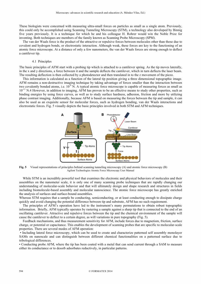
These biologists were concerned with measuring ultra-small forces on particles as small as a single atom. Previously, this could only be accomplished using Scanning Tunneling Microscopy (STM), a technology also developed by Binnig five years previously. It is a technique for which he and his colleague H. Rohrer would win the Noble Prize for inventing. Both techniques are members of the family known as Scanning Probe Microscopy (SPM). The van der Waals force is the product of the attractive or repulsive forces between molecules other than those due to covalent and hydrogen bonds, or electrostatic interaction. Although weak, these forces are key to the functioning of an atomic force microscope. At a distance of only a few nanometers, the van der Waals forces are strong enough to deflect a cantilever tip.
4.1 Principles
The basic principles of AFM start with a probing tip which is attached to a cantilever spring. As the tip moves laterally, in the x and y directions, a force between it and the sample deflects the cantilever, which in turn deflects the laser beam. The resulting deflection is then collected by a photodetector and then translated in to the z movement of the piezo. This information is calculated as a function of the lateral tip position giving a three dimensional topographic image. AFM remains a non-destructive imaging technique by taking advantage of forces smaller than the interaction between two covalently bonded atoms, i.e. 10-9 N. A typical atomic force microscope is capable of measuring forces as small as 10-11 N.4 However, in addition to imaging, AFM has proven to be an effective means to study other properties, such as binding energies by using force curves, as well as to study surface hardness, adhesion, friction and more by utilizing phase contrast imaging. Additionally, because AFM is based on measuring the forces between the tip and sample, it can also be used as an exquisite sensor for molecular forces, such as hydrogen bonding, van der Waals interactions and electrostatic forces. Fig. 5 visually depicts the basic principles involved in both STM and AFM techniques.
Fig. 5 Visual representations of principles behind scanning tunneling microscopy (A) and atomic force microscopy (B) Agilent Technologies Atomic Force Microscopy User Manual
While STM is an incredibly powerful tool that examines the electronic and physical behaviors of molecules and their assemblies on the nanometer scale, it is only one of many scanning probe techniques that are rapidly changing our understanding of molecular-scale behavior and that will ultimately design and shape research and structures in fields including biomolecule-based assembly and molecular nanoscience. The atomic force microscope has greatly enriched the analysis of surfaces and surface-bound assemblies. Whereas STM requires that a sample be conducting, semiconducting, or at least conducting enough to dissipate charge quickly and avoid changing the potential difference between tip and substrate, AFM has no such requirement. The principles of AFM’s operation have led to the instrument’s many permutations to obtain robust topographic information. Briefly, AFM typically operates by rastering a sample against a sharp tip that is connected to the end of an oscillating cantilever. Attractive and repulsive forces between the tip and the chemical environment of the sample will cause the cantilever to deflect to a certain degree, as will variations in pure topography (Fig. 5). Feedback mechanisms, and thus measurement sensitivity for AFM, include forces due to magnetism, friction, surface charge, or potential or capacitance. This enables the development of scanning probes that are specific to molecular-scale properties. There are several modes of AFM operation: • Including lateral force microscopy, which can be used to create and characterize patterned self assembly monolayer SAMs on nanoscale and can distinguish between different chemical functionalities on a patterned surface due to tribological differences. • Conducting probe AFM, where the tip has been coated with a metal that can send current through a SAM to measure either its conductance or to desorb adsorbates reductively, in particular patterns.
Microscopy: advances in scientific research and education (A. Méndez-Vilas, Ed.)__________________________________________________________________
© FORMATEX 2014594

Fig. 6 Schematic of AFM operation, A sharp tip resides at the end of a cantilever, rastering along a surface and detecting differences in features (illustrated here as dark stripes) The deflection of the AFM tip as a function of surface properties is recorded by shining a laser beam on the cantilever’s back, which is then sent to a position-sensitive photodiode [3]. AFM systems detect the z-displacement of the cantilever by the reflection of a laser beam focused on the top surface of the cantilever. The feedback from this sensor maintains the probe at a constant force. Interaction force: The z-axis (vertical) component of the force of interaction is calculated from the z-displacement of the cantilever and the spring constant of the cantilever. From Hooke's Law, F = - kz , where k is the spring constant. The spring constant for a cantilever is provided by the cantilever supplier or can be determined by the investigator. A constant force on the probe tip is maintained by feedback from measurement of the interaction force. The probe is moved up and down to maintain the measured constant force. Tapping mode: Tapping Mode imaging is implemented in ambient air by oscillating the cantilever assembly at or near the cantilever’s resonant frequency using a piezoelectric crystal. To image in fluids, the entire fluid cell is oscillated to drive the cantilever into oscillation. One of the most common modes utilized in imaging Atomic Force Microscopy is contact Mode. In Contact Mode, the tip is slowly lowered close to the sample to a set point predefined by the user. The sample is then scanned by rastering the tip across the surface. The laser beam aimed at the back of the cantilever detects changes in the deflection. The AFM tip must be attached to a cantilever with a very low spring constant (0.0001-5 N/m) so that it easily deflects when exposed to contact forces due to tip sampler repulsion, these forces range from 0.1-1000 nN. AFM in contact Mode can be performed in two modes, constant height or constant force, both modes utilize Hooke's Law, F = -k · Δx, where F is the repulsive force, k is the cantilever spring constant, and Δx is the cantilever deflection. In constant height mode, the probe scans the surface at a constant height and the tip deflection is recorded to give topography as a function of lateral position. This mode is typically used to image relatively flat surfaces. In constant force mode, the repulsive force between the tip and sample surface is kept constant due to a feedback loop controlling the z-axis motion of the piezo. This movement is then recorded and graphed to give a topographic image. The advantages of Contact Mode include high scan speeds "atomic resolution". However, the lateral forces caused by the rastering of the tip can distort the images, especially when scanning a softer sample such as DNA or proteins. Additionally, when imaging in air, capillary forces from a deposited fluid layer may cause large normal forces, introducing undesired artifacts. To overcome this limitation, when possible, contact Mode AFM is typically performed in liquid phase.
4.2 AC Mode
A newer approach that does not involve raster scanning of the surface is AC Mode. To perform a scan using this mode, the cantilever is oscillated at its resonant frequency, resulting in sinusoidal motion in the z-direction. In AC Mode, when the tip encounters changes in the elevation of the sample, the amplitude of the oscillation changes. In this situation, the feedback mechanism acts to keep constant amplitude, the set point value. The topography image is then generated by utilizing the voltage needed to move the z-position piezo actuator, which is multiplied with the piezo sensitivity given in nanometer/volt. Two subtypes of imaging have been derived from AC Mode, Noncontact, also called Attractive Mode due to net interactions being in the attractive regime of the potential curve, and Intermittent (Tapping Mode), which lies in the repulsive regime. In Figure 7, changes of force as a function of probe-sample separation are shown. Noncontact Mode relies on forces between the tip and the sample to affect oscillation, whereas Tapping Mode physically touches the surface at the bottom of the oscillation.
Microscopy: advances in scientific research and education (A. Méndez-Vilas, Ed.)__________________________________________________________________
595© FORMATEX 2014

Fig. 7 Plot of force as a function of probe-sample separation [4] Due to close approaches to the surface, cantilevers with stiff spring constants, typically between 20 - 100 N/m, are used to avoid sticking with the sample. Advantages of AC Mode in general include higher lateral resolution (1-5 nm) and no lateral forces leading to less damage upon softer samples, making AC Mode an ideal candidate to image biological samples. However, unlike contact Mode, AC Mode (vibrating mode,tapping) is often performed in air or gas as opposed to liquid due to dampening of the cantilever amplitude. If you carry out IC-AFM and monitor the phase signal, you are doing what is referred to as "phase imaging", i.e. generating a phase-contrast AFM image.
5. Transmission electron microscopy (TEM)
TEM operates on similar basic principles to those of an optic microscope, where electrons are used instead of light. A highly coherent beam of electrons is directed towards a sample which is specially prepared to thickness (< 200 nm) so that electrons can transmit through it (Fig. 8).An image is formed from the interaction of the electrons transmitted through the specimen; the image is magnified and focused onto an imaging device, such as a fluorescent screen, on a layer of photographic film, or to be detected by a sensor such as a CCD camera. TEMs are capable of imaging at a significantly higher resolution than light microscopes, owing to the small de Broglie wavelength of electrons.
Fig. 8 Schematic of TEM operation This enables the instrument's user to examine fine detail-even as small as a single column of atoms, which is thousands of times smaller than the smallest resolvable object in a light microscope. TEM forms a major analysis method in a range of scientific fields, in both physical and biological sciences. TEMs find application in cancer research, virology, materials science as well as pollution, nanotechnology, and semiconductor research. The contrast in a TEM depends on the specific TEM technique and conditions we are using. For example, for conventional bright field images, the darker areas of the image correspond to those regions of the sample where fewer electrons were transmitted through (i.e. thicker or denser).
Microscopy: advances in scientific research and education (A. Méndez-Vilas, Ed.)__________________________________________________________________
© FORMATEX 2014596

6. Nanostructures based on block copolymer self-assembly
Functional nanomaterials less than 100 nm in size have received extensive scientific and technological attention due to their potential applications in electronic, biomedical, and optical materials. This is because new and unexpected properties are less likely to develop with micron-scale bulk materials [5,6]. Block copolymer (BCP) self-assembly, one of the bottom-up methods in nanoscience and nanotechnology, has been used for the preparation of novel nanomaterials.
Fig. 9 Various microdomains of linear AB diblock copolymer
6.1 Phase behavior
BCPs consist of two or more chemically different polymers connected covalently. Due to their thermodynamic incompatibility and chain connectivity, the phase separation between two (or more) blocks occurs, only in the tens of nanometers range [7,8]. Fig. 8 shows the various microdomains (sphere, cylinder, double gyroid, and lamellar) observed for an AB coil coil type diblock copolymer depending on the block compositions. Furthermore, since metals, ceramics, and semiconductors can be incorporated into one or both blocks in a BCP [9,10], functional nanomaterials with various physical, chemical, electric, and magnetic properties can be prepared. In addition, since one block is easily removed from the self-assembled nanostructure, nanoporous templates with potential applications as scaffolds for creating functional nanostructured materials can be prepared [11,12].
7. Characterization of Block Copolymer Self-Assembly Nanostructures
Recently, block copolymer self-assembly nanostructure have been found special attention in various high-tech applications. These ordered nanostructures are useful for the fabrication of thermoplastic elastomers and can be applied in lithography, nanomaterials, and optoelectronic devices. Some of common techniques to characterize the self-assembly nanostructures presents as several examples in the next sections.
7.1 Applications of AFM
7.1.1 Study on the effect of solvent evaporation on ordering of microdomains in BCPs
Semicrystalline BCPs contain at least one crystallizable block. The polymer crystals usually have a thickness dimension of tens of nanometers. Such a size is comparable with the dimension of the microdomains formed by microphase separation. As shown in Fig. 9, after solvent annealing in benzene vapor, spin-coated PS-b-PEO film showed a high degree of long-range lateral ordering of PEO cylindrical microdomains vertically that are aligned to the substrate [13].
Fig. 10 Long-range ordering of cylindrical microdomains of PEO in PS-b-PEO thin films annealed in a benzene vapor[13]
Microscopy: advances in scientific research and education (A. Méndez-Vilas, Ed.)__________________________________________________________________
597© FORMATEX 2014

7.1.2 Study on the effect of chain length and surface in crystallization
Long-range ordering thin film morphology of semicrystalline BCPs and the control of the thin film morphology through crystallization-related technologies could be studied by AFM. Figures 11(a) and 11(b) show PEO-b-PBO BCPs which are different in chain length. Figure 11(a) and 11(c) show PEO-b-PBO BCPs with same chain length and different crystallization substrate.
Fig. 11 (a) A two-dimensional spherulite morphology [14] (b) A rounded plaque [15] (c) A fractal dendritic structure [16]
7.1.3 Study on micelle formation in BCPs
When BCPs are dissolved in a selective solvent, micelles with a soluble corona and insoluble core can be formed at a concentration higher than the critical micelle concentration (CMC). The driving force for the formation of micelles is the solvophilic/solvophobic force. Block copolymer micelles can be used as nanocarriers for drugs and catalysts and have wide applications in the fields of biomedical material and catalysis. Xu team [17] cross- linked the PB core of solid-state morphologies to prepare “Janus” micelles (i.e., noncentrosymmetric micelles consisting of two different hemispheres; Fig. 12.
Fig. 12 Janus micelles with a cross-linked PB core and PMMA/PS shell hemispheres. After PB cross-linking in bulk (left) the aggregates were dissolved in water-forming Janus-type micelles. Further deprotection of the methyl groups of PMMA, and dissolution in water, collapsed the PS-block and formed highly ordered “super micelle” structures [18, 19].
Firstly, a PS-b-PB-b-PMMA triblock copolymer was prepared in the bulk state, in which the PB minority blocks formed spherical microdomains located at the interfaces of a PS-b-PMMA lamellar microdomains structure which confirmed by AFM method. These workers took advantage of the PB core in the morphology to cross-link it. Characterization of the nanostructure stabilized in dioxane revealed the formation of Janus-shaped micelles. Furthermore, after hydrolysis of the PMMA block, which afforded PAA, dispersion of the micelles in water resulted in the collapse of the PS block. In a concentration range above the CMC, several PS hemispheres of these micelles aggregated to form what the authors called “supermicelles.”
7.1.4 Study on hierarchical assemblies of supramolecules in BCPs
The hierarchical assemblies of supramolecules, which consisted of polystyrene-b-poly(4- vinylpyridine) (PS-b-P4VP) with 3-pentadecylphenol (PDP) hydrogen-bonded to the 4VP, were investigated in thin films after solvent annealing in a chloroform atmosphere. Figure 12 shows chemical structure of the mentioned block copolymer. The synergistic co-assembly of PS-b-P4VP and PDP was utilized to generate oriented hierarchical structures in thin films. Hierarchical assemblies, including lamellae-within-lamellae and cylinders-within-lamellae, were simultaneously ordered and oriented from a few to several tens of nanometers over macroscopic length scales.
Microscopy: advances in scientific research and education (A. Méndez-Vilas, Ed.)__________________________________________________________________
© FORMATEX 2014598

(a) (b)
(c)
Fig. 13 (a) Chemical drawing of the diblock copolymer-based supramolecule: PS-b-P4VP (PDP). (b) AFM height and phase image of a SP1 thin film, ~47 nm in thickness. The z scale is 30 nm for height and 15° for phase. (c) In-plane TEM image of a ~50 nm SP1 thin film (SP1 is based on PS(31900)-b-P4VP(13200) and forms a gyroid morphology).
7.2 Applications of SPM
7.2.1 Study on hierarchical assemblies of supramolecules in BCPs
The lamellar and cylindrical microdomains with a periodicity of ~40 nm, could be oriented normal to the surface, while the assembly of comb blocks, P4VP(PDP), with a periodicity of ~4 nm, were oriented parallel to the surface. Furthermore, using one PS-b-P4VP copolymer, thin films with different hierarchical structures, i.e., lamellae-within lamellae and cylinders-within-lamellae, were obtained by varying the ratio of PDP to 4VP units. The hierarchical assemblies of supramolecules, which consisted of polystyrene-b-poly(4- vinylpyridine) (PS-b-P4VP) with 3-pentadecylphenol (PDP) hydrogen-bonded to the 4VP, were investigated in thin films after solvent annealing in a chloroform atmosphere.
Fig. 14 SPM images of (a) SP1, 88 nm in thickness, (b) SP2, 80 nm, and (c) SP4, 50 nm, thin films after spin-casting. The z scale for height and phase is 10 nm and 15° for (a) and 15 nm and 65° for (b) and (c).Macromolecules, Vol. 41, No. 17, 2008 Figure 14b shows SPM images of a ~47 nm SP1 thin film after annealing in chloroform for 48 h. SP1 is based on PS(31900)-b-P4VP(13200) and forms a gyroid morphology. A fingerprint-like pattern, with a domain spacing of ~40 nm, is seen. Similar patterns were observed in the in-plane TEM image shown in Figure 14c. Although the samples for SPM and TEM studies were prepared on two different substrates, i.e., silicon wafers and NaCl plates, differences in
Microscopy: advances in scientific research and education (A. Méndez-Vilas, Ed.)__________________________________________________________________
599© FORMATEX 2014

morphologies were not evident. We also floated the supramolecular thin films off the NaCl substrate. Upon imaging the bottom of the films, we observed SPM images similar to Fig. 14. In the bulk, SP1 forms gyroidal morphology. The observed fingerprint-like pattern in Figure 13 indicates that the lamellar microdomains are oriented normal to the surface. This may be due to the preferential swelling of the PS domain by chloroform or the salvation of the PDP in the PS domain, both of which increase the PS volume fraction.
7.2.2 Study on effect of blocks ratio on nanostructure assemblies’ formation in BCPs
The BCP-based supramolecular thin films described here offer numerous opportunities to fabricate functional devices. The microdomains can be oriented normal to the surface without surface modification. Since BCP-based supramolecules can be easily prepared by attaching small molecules to a copolymer, various built-in functionalities can be readily incorporated (Figure 15).
Fig 15 SFM height and phase image pattern of (a) a 50 nm SP5-1 thin film, showing a parallel lamellae-within-lamellae morphology; (c) a 62 nm SP5-2 thin film, showing a mixed morphology of parallel and perpendicular lamellae-within-lamellae. The z scale for height and phase is 20 nm and 40° for (a) 30 nm and 50° for (c). The fundamental principles outlined here should be potentially Block-Copolymer-Based Supramolecules in Thin Films applicable to other systems. Thin films of BCP-based supramolecules may find numerous applications in the fabrication of functional nanodevices.
7.3 Applications of TEM
7.3.1 Study on PBD-POSS assembly
Transmission Electron Microscopy (TEM) has been used in study of hybrid organic –inorganic polyhedral oligomeric silsesquioxanes (poss) based block copolymers recently. Zheng et al. synthesized random copolymers of POSS and butadiene. In PEPOSS composites, PE competes with POSS for crystallization, thus polybutadiene – POSS composites were synthesized to study the POSS crystallization/aggregation without the polymer host competing for crystallization. Also it was anticipated that POSS hard blocks would reinforce the soft polybutadiene materials to give elastomeric properties for PBD-POSS composites. Fig. 15 shows the TEM image of PBD-POSS with 12wt % (A) and 43 wt % POSS (C). In Fig. 15.A, POSS aggregates were directly observed as short randomly oriented lamellae with the lateral dimensions of approximately 50 nm. The thickness of the lamellae was found to be approximately 3-5 nm and corresponded to roughly twice the diameter of POSS nanoparticle. Increasing the POSS ratio to 43 wt % resulted in continuous lamellae with lateral lengths on the order of microns (Fig 15.C). The morphology bears similarity to the lamellar morphology formed by precise diblock copolymers.
7.3.2 Study on PS-POSS assembly
Recently Hirai et al. synthesized PS-POSS and PMMA-POSS diblock copolymers by anionic polymerization.76 Sec-butyl lithium was used as the initiator, PMMA or PS block were first synthesized and POSS was added as the second block. The volume fraction of PS: POSS and PMMA:POSS were maintained close to 0.5.
7.3.3 Study on solvent in polymerization
Some multi-block copolymer based assemblies which are formed in various solvents are shown in Fig. 16
Microscopy: advances in scientific research and education (A. Méndez-Vilas, Ed.)__________________________________________________________________
© FORMATEX 2014600

Fig. 16 (A) TEM of PBD-POSS. (Fig. taken from Zheng, L.; Hong, S.; Cardoen, G.; Burgaz, E.; Gido, S. P.; Coughlin, E. B. Macromolecules 2004, 37, 8606-8611. The morphology of the diblock copolymer was studied by SAXS, TEM and WAXS. Lamellae of POSS and PS were obtained and the TEM images are shown in Figure 17.
Fig. 17 (Right) Chemical structure of PMMA-POSS and PS-POSS copolymer and (left) TEM image of the corresponding copolymer (fig. taken from reference, Hirai, T.; Leolukman, M.; Hayakawa, T.; Kakimoto, M.; Gopalan, P. Macromolecules 2008, 41, 4558-4560.
Fig. 18 TEM of assemblies formed in selective solvent conditions by multiblock copolymers: (a) Janus spheres, (b) core-shell spheres, (c) raspberry-like spheres, (d) Janus cylinders, (e) core-shell cylinders,(f) segmented cylinders , (g) asymmetric (Janus) membrane vesicles, (h) double-layer membrane vesicles, and (i) vesicles with hexagonally packed cylinders Bar 50nm. Liang GD, Xu JT, Fan ZQ, Mai SM, Ryan AJT. , Macromolecules 2006; 39:5471-8
Microscopy: advances in scientific research and education (A. Méndez-Vilas, Ed.)__________________________________________________________________
601© FORMATEX 2014
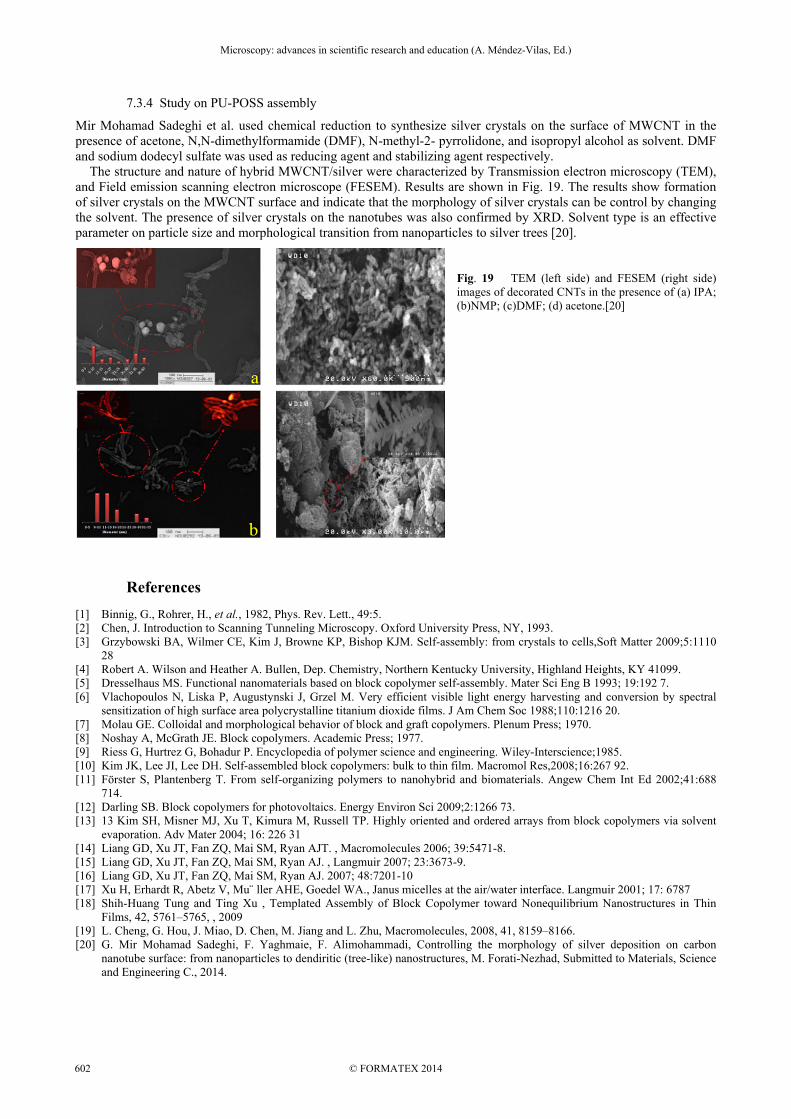
7.3.4 Study on PU-POSS assembly
Mir Mohamad Sadeghi et al. used chemical reduction to synthesize silver crystals on the surface of MWCNT in the presence of acetone, N,N-dimethylformamide (DMF), N-methyl-2- pyrrolidone, and isopropyl alcohol as solvent. DMF and sodium dodecyl sulfate was used as reducing agent and stabilizing agent respectively. The structure and nature of hybrid MWCNT/silver were characterized by Transmission electron microscopy (TEM), and Field emission scanning electron microscope (FESEM). Results are shown in Fig. 19. The results show formation of silver crystals on the MWCNT surface and indicate that the morphology of silver crystals can be control by changing the solvent. The presence of silver crystals on the nanotubes was also confirmed by XRD. Solvent type is an effective parameter on particle size and morphological transition from nanoparticles to silver trees [20].
Fig. 19 TEM (left side) and FESEM (right side) images of decorated CNTs in the presence of (a) IPA; (b)NMP; (c)DMF; (d) acetone.[20]
References
[1] Binnig, G., Rohrer, H., et al., 1982, Phys. Rev. Lett., 49:5. [2] Chen, J. Introduction to Scanning Tunneling Microscopy. Oxford University Press, NY, 1993. [3] Grzybowski BA, Wilmer CE, Kim J, Browne KP, Bishop KJM. Self-assembly: from crystals to cells,Soft Matter 2009;5:1110
28 [4] Robert A. Wilson and Heather A. Bullen, Dep. Chemistry, Northern Kentucky University, Highland Heights, KY 41099. [5] Dresselhaus MS. Functional nanomaterials based on block copolymer self-assembly. Mater Sci Eng B 1993; 19:192 7. [6] Vlachopoulos N, Liska P, Augustynski J, Grzel M. Very efficient visible light energy harvesting and conversion by spectral
sensitization of high surface area polycrystalline titanium dioxide films. J Am Chem Soc 1988;110:1216 20. [7] Molau GE. Colloidal and morphological behavior of block and graft copolymers. Plenum Press; 1970. [8] Noshay A, McGrath JE. Block copolymers. Academic Press; 1977. [9] Riess G, Hurtrez G, Bohadur P. Encyclopedia of polymer science and engineering. Wiley-Interscience;1985. [10] Kim JK, Lee JI, Lee DH. Self-assembled block copolymers: bulk to thin film. Macromol Res,2008;16:267 92. [11] Förster S, Plantenberg T. From self-organizing polymers to nanohybrid and biomaterials. Angew Chem Int Ed 2002;41:688
714. [12] Darling SB. Block copolymers for photovoltaics. Energy Environ Sci 2009;2:1266 73. [13] 13 Kim SH, Misner MJ, Xu T, Kimura M, Russell TP. Highly oriented and ordered arrays from block copolymers via solvent
evaporation. Adv Mater 2004; 16: 226 31 [14] Liang GD, Xu JT, Fan ZQ, Mai SM, Ryan AJT. , Macromolecules 2006; 39:5471-8. [15] Liang GD, Xu JT, Fan ZQ, Mai SM, Ryan AJ. , Langmuir 2007; 23:3673-9. [16] Liang GD, Xu JT, Fan ZQ, Mai SM, Ryan AJ. 2007; 48:7201-10 [17] Xu H, Erhardt R, Abetz V, Mu¨ ller AHE, Goedel WA., Janus micelles at the air/water interface. Langmuir 2001; 17: 6787 [18] Shih-Huang Tung and Ting Xu , Templated Assembly of Block Copolymer toward Nonequilibrium Nanostructures in Thin
Films, 42, 5761–5765, , 2009 [19] L. Cheng, G. Hou, J. Miao, D. Chen, M. Jiang and L. Zhu, Macromolecules, 2008, 41, 8159–8166. [20] G. Mir Mohamad Sadeghi, F. Yaghmaie, F. Alimohammadi, Controlling the morphology of silver deposition on carbon
nanotube surface: from nanoparticles to dendiritic (tree-like) nanostructures, M. Forati-Nezhad, Submitted to Materials, Science and Engineering C., 2014.
Microscopy: advances in scientific research and education (A. Méndez-Vilas, Ed.)__________________________________________________________________
© FORMATEX 2014602