advances e detectors - jaxatakahasi/download/takahashi_review_ndip0… · advances e detectors...
TRANSCRIPT

Recent Advanceson CdTe/CdZnTe detectors
Tad TakahashiInstitute of Space and Astronautical Science (ISAS)
Japan Aerospace eXploration Agency (JAXA)and
Univ. of Tokyo
Acknowledgement : Z. He(Michigan), P.Luke (LBNL), F. Harrison(Caltech), O. Limousin(CEA), C. Szeles (eV), R. Ohno(ACRORAD), J. Matteson (UCSD)
For High Energy PHOTON
NDIP08
T.Takahashi

Outline
• Demand and CdTe/CdZnTe
• Recent Progress on technology• Crystal and ASIC
• X-ray Imager• Pixel & Strips
• Gamma-ray Detector• Coded Mask /PET
• Compton Camera
• Summary/Future Prospects
NDIP08
T.Takahashi

Demands
3
In the field of Medical ApplicationHomeland SecurityAstronomical Observation
Need Detector Material which can be used as an alternative to Si (in terms of Efficiency) an alternative to Ge (in terms of Operating Temperature) Good Energy Resolution similar to Ge (0.2%@662keV)
High Efficiency, above 10 keV upto 1 MeVPosition resolution a few hundred micronA detector can be operated at room temperature
!""#$%&'%("%)"*+%,-./01&%23,%4'01,%3"",%23'&5"*%67%&'%87%+"2*$%%9'*%&5"%:321%23$4"*
NDIP08
T.Takahashi

All next generation telescopes need a Hard-X camera above 10 keV, where Si becomes transparent
4
NuSTAR Small Explorer
Two hard X-ray (6 - 79 keV) focusing telescopes
Launch August 2011
17h12m17h14m17h16m
-39d30m
-40d00m
NeXT Mission(JAPAN)
Launch 2013 Launch 2014
Simbol-X(ASI/CNES)
To take a photo ofSuperNova explosion
in hard X-ray
NDIP08
T.Takahashi

With Newly developedHard X-ray Mirror
Mirror Detector10-20 m
Nagoya U.
NDIP08
T.Takahashi

• High Z semiconductor (ZCd = 48, ZTe = 52), ! =5.9 g/cm3
• Room Temperature Operation or Cool Environment
P. Luke (2006)
100 keV
511 keV
Takahashi and Watanabe (2000)
CdTe/CdZnTe seem to be the only candidateat least, at this moment
NDIP08
T.Takahashi
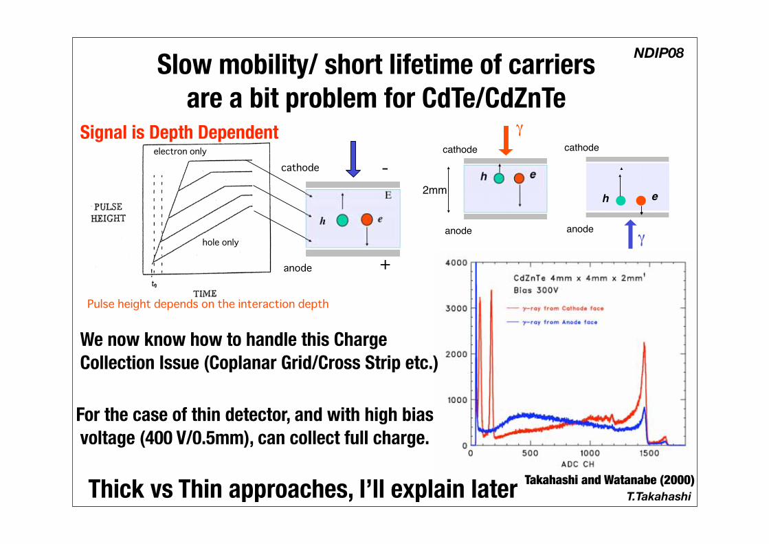
Slow mobility/ short lifetime of carriers are a bit problem for CdTe/CdZnTe
!"#$%&'
"(%&'
eh
)*+,'-$'./$#-&'0'(&,-%(-#$'-.(#'1"!#.%(-&'0#$
!
2
3'+'!#1%(-%(+4
$%+'-%(+4
cathode
anode
eh
"
2mm
cathode
anode
eh
"
We now know how to handle this Charge Collection Issue (Coplanar Grid/Cross Strip etc.)
For the case of thin detector, and with high bias voltage (400 V/0.5mm), can collect full charge.
Thick vs Thin approaches, I’ll explain later
Signal is Depth Dependent
Takahashi and Watanabe (2000)
NDIP08
T.Takahashi

CdTe/CdZnTe seem to be the only candidateat least, at this moment
137Cs
FWHM2.1 keV0.3 %
662keV
CdZnTe
epoxy
gold stud
ASIC
CdTe/ACRORAD
NuSTAR/Caltech
Takahashi et al. 2005
Thin CdTe diode at -20 deg
260 eV at 6.4 keV
NDIP08
T.Takahashi
Because, they’ve already shown good performance

CdTe/CdZnTe Commercial ProductsAmptek AXION
aguila (US)
Radiation-Threat-DetectorX-ray Spectrometer
CdTe dental panoramic digital imaging system
NDIP08
T.Takahashi

Courtesy of AJAT (Finland)
CCDScintillator
CMOS
CdTeCMOS
NDIP08
T.Takahashi

Hard X-ray ImagerIntegrated type
Commercial Products
AJAT, Finland
1 dim Imager (30cm)
100 micron pitch
NDIP08
T.Takahashi

Technologies
Crystal&
ASIC
NDIP08
T.Takahashi

Who makes CdTe/CdZnTe Crystal?
From a review talk by P.J. Sellin (2005)
NDIP08
T.Takahashi

Recent Advances on TechnologiesACRORAD (JAPAN)
Quartz ampoule
CdTe poly crystal
Te-rich Cl-doped Cd-Te solvent
Heater unit
Cl-doped CdTe grown single crystal
CdTe single crystal seed
!"#$%&'(%#)%"'*%)+,-'.!(*/
0#"%12&')"%#)3%4)',1'5,6)'+%#)748
9%":'2471,"3';#1%"
Large Single Crystal
!(*
1st Large Scale CdTe Camera in Space (INTEGRAL)
NDIP08
T.Takahashi

Recent Advances on Technologies
!"
#"!"#$%&''()()*++
eV Products (High Pressure Bridgman and improved method)
Large Crystal
SWIFT !-ray satellite (2004-)
NDIP08
T.Takahashi

Recent Advances on TechnologiesREDLEN
succeeded to make CZT by THMLarge Single Crystal
Chen et al. JAP, 2008
662 keV 1. 18% (7.8 keV, FWHM)without additional signal correction)
2 x 2 x 1.05 cm3
monolithic pixel pixel size 2.46 mm
IR imagevery small Te
precipitate/inclusion
NDIP08
T.Takahashi

We need ASIC : If you need CdTe/CdZnTe imaging detectors
Level-sensitive
Discriminator
Semigaussian“fast” shaper
Monostable(fixed width)
Semigaussian“slow” shaper
ChargeIntegrator(preamp.)
S/H Vss
Vdd
TriggerOut
TAVA
Multiplexer
analog out
ADCSpectrum
Photon Counting
Need 50 e- at 0pF for both cases
NDIP08
T.Takahashi

Hard X-ray Camera
For photonsabove 10 keVbelow 100 keV
NDIP08
T.Takahashi

CdTe Photon-counting imager using XPAD chip
!"#"$%&'(&"$)&*&+,-.&/001
0.7 mm thick CdTe20 kpixels (130!m x 130!m) 2 ms/frame 106 photons/pixel
NDIP08
T.Takahashi
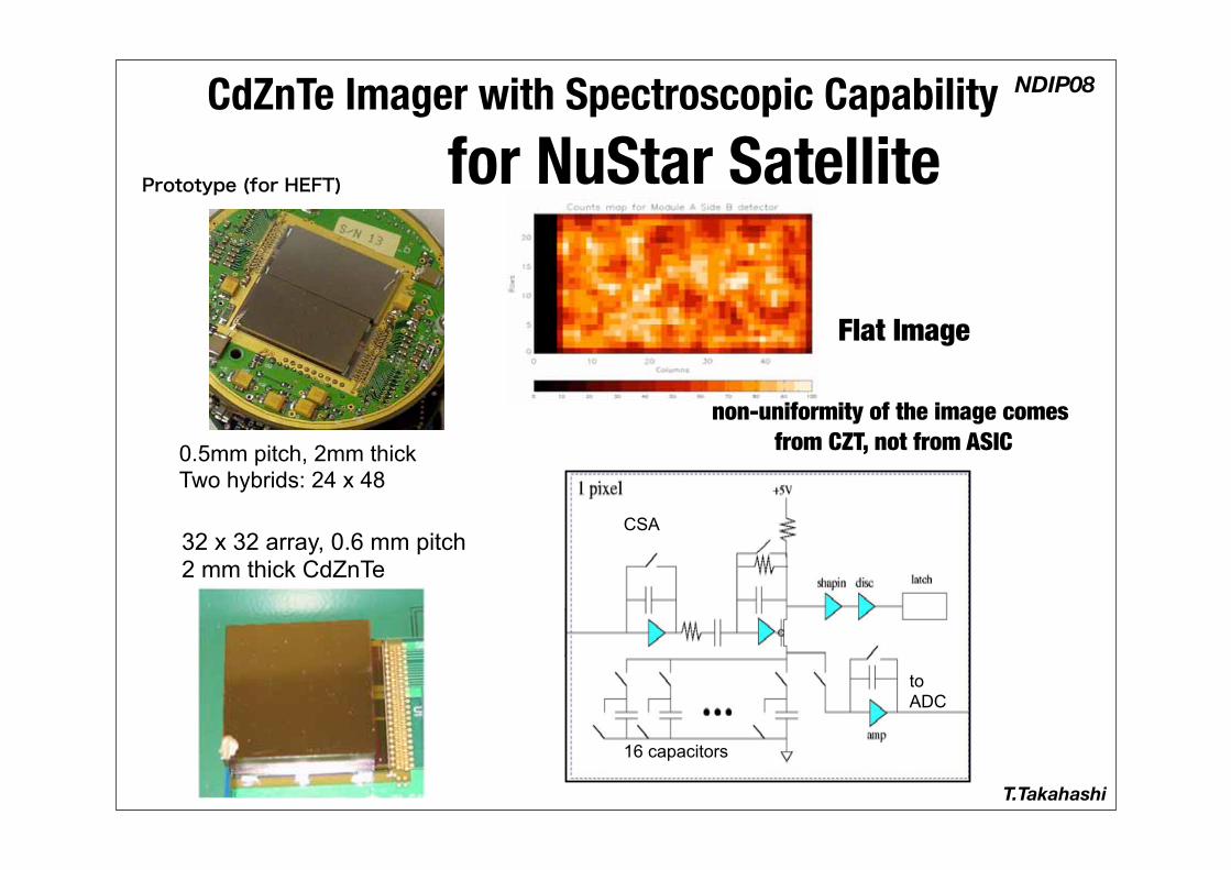
16 capacitors
CSA
toADC
for NuStar Satellite
32 x 32 array, 0.6 mm pitch 2 mm thick CdZnTe
CdZnTe Imager with Spectroscopic Capability
non-uniformity of the image comes from CZT, not from ASIC
!"#$#$%&'()*#"(+,-./
Flat Image
0.5mm pitch, 2mm thickTwo hybrids: 24 x 48
NDIP08
T.Takahashi

for NuStar Satellite
32 x 32 array, 0.6 mm pitch 2 mm thick CdZnTe
CdZnTe Imager with Spectroscopic Capability
non-uniformity of the image comes from CZT, not from ASIC
!"#$#$%&'()*#"(+,-./
Flat Image
0.5mm pitch, 2mm thickTwo hybrids: 24 x 48
E
coun
ts
5 mm CdZnTe, 800 V, 1C Single pixel 155Eu 900 eV FWHM @ 86 keV
F. Harrison, 2008
NDIP08
T.Takahashi

! HED: mosaic of 64 independent CdTe (Al/CdTe/Pt) cameras! Caliste 64: first prototype of detection unit
! See A. Meuris’ talk in this session
241Am spectrum at -10°C, 500V with the single events of the 64 pixels
0.66 keV fwhm @ 13.94 keV0.84 keV fwhm @ 59.54 keV
for Simbol-X SatelliteCdTe Imager with Spectroscopic Capability NDIP08

5 cm
ISAS/JAXA
Large Area 1024 pixel CdTe Array(pixel size 1.4 x 1.4 mm2)
Large Area Hard X-ray Imager
0.5 mm thick
NDIP08

X-ray Imager
201Tl99mTc
69-80 keV140 keV
Allow us to study where in the leaf absorb which kind of metal
(multi-tracer imaging)
NDIP08

Fine Pitch CdTe Strips!"#$%&'()*+,-+.%/0')1+1&+234#+(1"%5(+&6+17#+83""%#"+#)#01"&9#+:;6-+<&"+=9>#+9%&9#?@-+A%"#B8&69+9&#(+6&1+C&"4+&6+=9>#?+A%17+6#C+#)#01"&9#+231#"%3)&6+=9>#+:D)+3(+36&9#E!1+3(+0317&9#-C#+73$#+('00##9#9+1&+234#+F6#+5%107+.&'8)#+G%9#9+="&((+G1"%5+9#1#01&"
CdTe
ASIC
ASIC
ceramic board with through holesIn/Au stud bump
wire-bonding
wire-bondingstrip electrode
!"#$%&%$"'(&)**+,**&-$'#./
NDIP08

x [ch]0 10 20 30 40 50 60
y [c
h]
0
10
20
30
40
50
60
0
20
40
60
80
100
120
140
!"#$%
x [ch]0 10 20 30 40 50 60
y [c
h]
0
10
20
30
40
50
60
0
20
40
60
80
100
120
140&'#$%
x [ch]0 10 20 30 40 50 60
y [c
h]
0
10
20
30
40
50
60
0
20
40
60
80
100("#$%
x [ch]0 10 20 30 40 50 60
y [c
h]
0
10
20
30
40
50
60
0
20
40
60
80
100"))#$%
Results(imaging)Shadow Image
nut(M3)
nut(M2)washer(M3)
solder
(0.6mm)
!x~400!m Imaging Spectroscopy !!
various RIs(241Am, 133Ba, 57Co)
–20ºC, 500V bias
spectra
241Am133Ba57Co
NDIP08

Gamma-ray
above 100 keV
NDIP08
T.Takahashi

CdTe & CdZnTe detectors for gamma-rayThick Approach
!"#$%&'()$**+)(#+,#$'(-$# P.Luke (LBNL)
NDIP08
T.Takahashi

Gamma-ray Detector
Cross Strip CdZnTe
511keV3.1 % FWHM
California Breast Cancer Research Program, CBCRP Grant Number 12IB-0092
For a Large NIH Program 1 mm spatial resolution, ~2% energy resolution at 511 keV
by C. Levin of Stanford,and J. Matteson et al. 2008
NIH Grant #R01CA120474
Edge on geometryEff. of 86 % for 511 keVby 4cm CZT
!"#$%&'())"*$+(,-.&/0+,1&'2$%(3"45,(3"&
6,7(8
NDIP08
T.Takahashi

Gamma-ray Detector
Mini Coded Mask (cross strip CZT)
J. Matteson &Aguila Tech., 2008
supported by HSRAPA
Redlen CZT
DGAS specs:!- Image a 5 mCi source at >5 m in less than 10 sec, and localize it to <10 degrees!- Energy band of 40 - 250 keV!- Better than 10% energy resolution at 122 keV
NDIP08
T.Takahashi

CdTe & CdZnTe detectors for gamma-rayThin Approach
40 layer = 20 mm thick CdTe
!Concept
Full Charge Collection (No Tail)-> Stack thin CdTe layersto get high efficiency.
!"#$%&%'%&%(()*+,-.#//%010&%((23*"##%4$5#"/6
AmptekXR-100T-CdTe-STACK
Watanabe, TT et al. 2002
NDIP08
T.Takahashi

Gamma-ray Detector
CdTe PET (1st Result) Achieved Spatial Resolution< 1mm!""#$%&'%())*())*+))%
+(,-%./01%2!3
Rat Mouse
Brain
Tohoku Univ.
Press Release by K. Ishii, Tohoku Univ., Japan
Edge on geometry
NDIP08
T.Takahashi

Gamma-rayCompton Camerafor High Sensitivity
Imaging
NDIP08
T.Takahashi

Z. He et al. Michigan U. (2008)
• Cathode/Anode Ratio (Depth Info)• Timing Measurement (Drift Time) ( Multiple Interaction/ Depth Info)
Gamma-ray Detector
CdZnTe Compton Camera (Thick)
2!2!1.5 cm3 = 6 cm3 CZT(eV Products)
ASIC front-end(Gamma-Medica-Ideas AS)
NDIP08
T.Takahashi

Room-temperature handheld CdZnTe !-ray imaging spectrometers with energy resolution ~ 1% FWHM at 662 keV
NDIP08
T.Takahashi
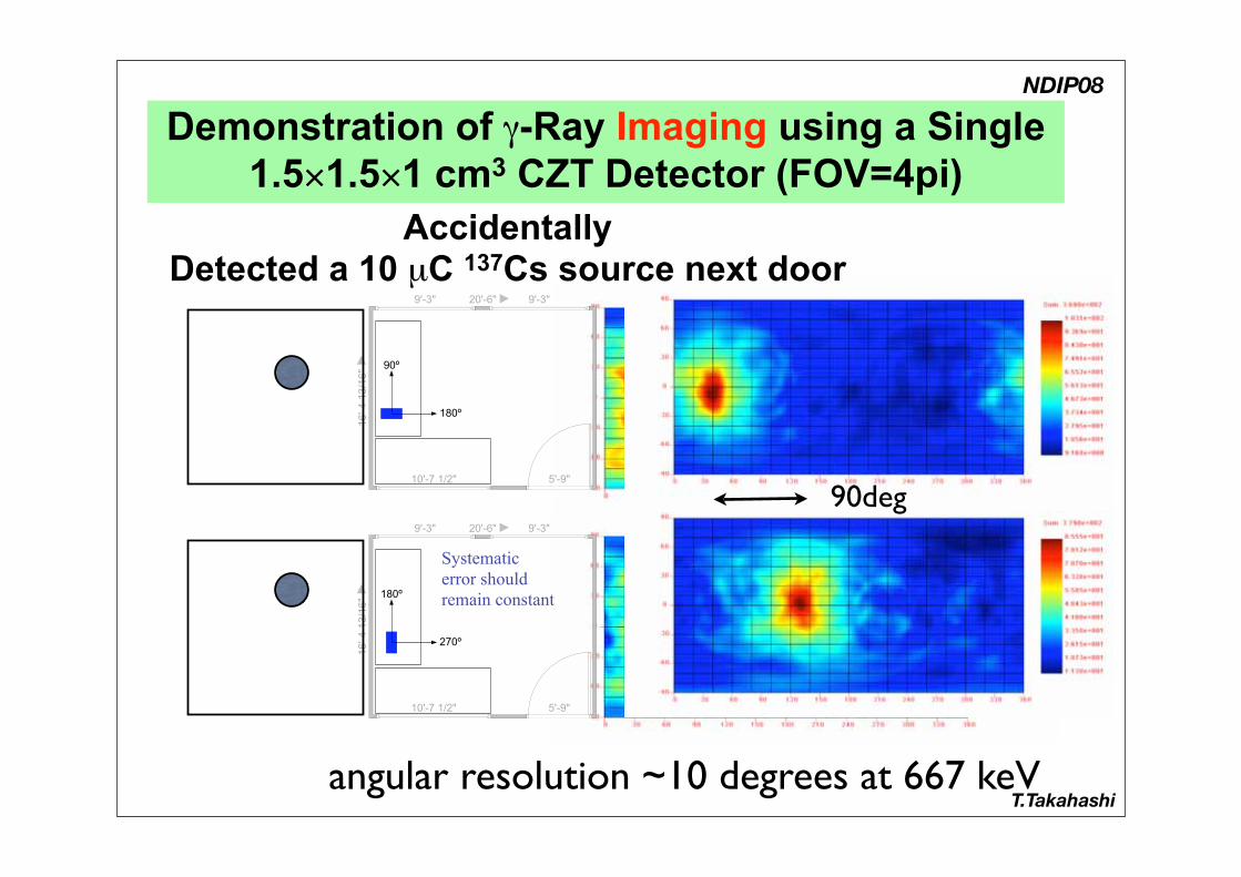
Systematicerror shouldremain constant
Demonstration of !-Ray Imaging using a Single 1.5"1.5"1 cm3 CZT Detector (FOV=4pi)
angular resolution ~10 degrees at 667 keV
AccidentallyDetected a 10 !C 137Cs source next door
90deg
NDIP08
T.Takahashi

Gamma-ray Detector
Si/CdTe Compton Camera (Thin)!"#"$%&%'()*+,-.'/012%345'6"44%7'"&'!"#$'
89%:'%;#413"<1$'=-3"5'*%4%&61#%>?)"@%44A@%'
:A44'B&%'A@'013'@C%'&%$&A<D%'2%"&B3%2%$@'
0312'EFF'G%H'@1'IFF'G%HJ
%&'&('&)"*+')",&-"'*('.%-*/"0"012'&A$6%'A@'A&'41:'K'2"@%3A"4'"$7'212%$@B2'10'%4%6@31$'
"31B$7'@C%'$B64%A'A&'&2"44'-L'M%&&'"N%6@%7'O5'P1##4%3'
Q31"7%$A$R
Concept (Takahashi et al. SPIE 2003).Narrow FOV (field-of-view)
Compton camera.Compton kinematics to
suppress backgrounds
34''+*5"0('67'89:';;'
<=&->'%&'?&@"+
A'+*5"0('67'89B:';;'
<=&->'C)$"'?&@"+
D'EF&<
NDIP08
T.Takahashi

Gamma-ray Detector
Si/CdTe Compton Camera!"#$#$%&'
Angular resolution ~3 degrees at 511 keV 0 100 200 300 400 500 6000
50
100
150
200
250
energy
Z
DSSDs
CdTe Bottom
CdTe Side47.4
14.4
X
47.4
source direction
Compton cone
!"#$%&%'()$*+
,-%&%'()$*+
.//%0$1%23-45%+36*7$%89:.%"$;*$$+<
=>?%"$;%@A1
.//%0$1
NDIP08
()*+',*-'$-*./-0111-23-45567 T.Takahashi

Good performance for both multiple and diffuse sources. Large FOV and good energy resolution
!"#$%
!"&$%
Si/CdTe Compton Camera NDIP08
'()*+,)-+.-)/0-1222-34-56678
ISAS, 2008
T.Takahashi

Summary/Future Prospects1. CdTe and CdZnTe are now in the phase ofreal application.2. Large and Thin CdTe wafers are widely used for the commercial products of hard X-ray camera3. Photo Counting Detector (109-1010 photons/pixel /s)would be the next step.4. For gamma-ray detection, Thick approach and Thin approach both work.5. Homeland Security and Medical Imaging boost the development6. Space missions are always one step ahead in terms of technological requirements, which is good.
NDIP08
T.Takahashi