advanced on-board processor (a.0.p.)
TRANSCRIPT

FINAL REPORT
ADVANCED ON-BOARD PROCESSOR (A.0.P.)
NAS 5-20278
Prepared for
NATIONAL AERONAUTICS AND SPACE ADMINISTRATION
Goddard Space Flight Center 1 j
Greenbelt, Maryland co
Reproduced by
NATIONAL TECHNICALINFORMATION SERVICE
US Department of CommerceSpringfield, VA. 22151
Prepared by
WESTINGHOUSE ELECTRIC CORPORATION
Defense and Electronic System Center
Baltimore, Maryland
(NASA-CR-132851) ADVANCED ON-BO-D N7410183
PBOCESSOR (AOP) Final Report
(Westinqhouse Electric Corp.) p HC"' CSCL 09B Unclas
G3/0 8 21807

-- - Aerospace Division
Final Report
Advanced On-board Processor(AOP)
June 15, 1973
prepared by
Westinghouse Electric Corporation
Defense and Electronic Systems Center
Baltimore, Maryland
for
The National Aeronautics and Space Agency
Goddard Space Flight Center
Greenbelt, Maryland
7

9 -- Aerospace Division
TABLE OF CONTENTSPAGE
1.0 LIST OF TABLES & FIGURES 1
2.0 INTRODUCTION 3
3.0 AOP BREADBOARD 11
3.1 Circuits 11
3.2 Mechanical Features 11
3.3 Test Panel and Memory 13
3.4 Breadboard Checkout 13
4.0 CUSTOM METALLIZED MULTIGATE ARRAYS (CMMA) 14
4.1 LSI Circuit Description 14
4.1.1 Die Organization 15
4.1.2 LSI Configuration 15
4.2 Circuit Layout 21
4.3 CMMA Layout 21
4.4 Testing 21
4.5 Equation Development and Specifications 21
4.6 Circuit Characterization 25
4.7 Final Circuit Development 25
4.8 Generation of New Equations 25
5.0 CMMA BREADBOARD 26
5.1 Fabrication 29
5.1.1 Contactors 30
5.1.2 Printed Circuit Board 30
5.1.3 Board Rack and Back Panel 31
5.1.4 Wiring List 31
5.2 Testing .. 31
Preceding page blank
iii

@ - Aerospace Division
TABLE OF CONTENTS
(continued)
PAGE
6.0 ENGINEERING MODEL AOP 32
6.1 CMMA Package 33
6.2 Multilayer Board Fabrication 35
6.2.1 Multilayer Board Types 35
6.2.2 Multilayer Board Configuration 35
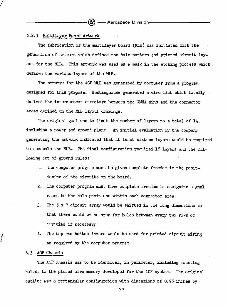
6.2.3 Multilayer Board Artwork 37
6.3 AOP Chassis 37
6.4 Assembly 39
6.4.1 Multilayer Board Changes 39
6.4.2 CMMA Circuit Assembly 40
6.5 Tests 40
Appendix
iv

- Aerospace Division
PAGE
1.0 TABLE AND FIGURES
1.1 Tables
2-1 AOP Characteristics 4
2-2 List of On-Board Computer Functions 10
3-1 AOP Breadboard Partitioning 12
4-1 Standard Gate Specifications (original) 22
4-2 Driver Gate Specifications (Original) 23
4-3 Circuit Specification Temperature Range (original) 24
4-4 Revised Equations 27
4-5 Circuit Specification Temperature Range (final) 28
6-1 Multilayer Board Wiring Changes 41
Appendix
A-1 AOP Characteristics (Table 201) A-6
1.2 Figures
2-1 Typical AOP Stacked Configuration 5
2-2 AOP System Block Diagram 8
2-3 Reliability Models 9
4-1 Die Organization 16
4-2 Standard Gate Schematic 17
4-3 Driver Gate Schematic 18
4-4 Extender/Pull-Up Cell 19
4-5 Propagation Delay Measurement Setup 20
1

® - Aerospace Division
PAGE
6-1 CMMA Package 34
Appendix
A-1 AOP Unit A-2
A-2 Typical AOP Stacked Configuration A-3
A-3 AOP Block Diagram A-4
A-4 AOP System Configuration A-5
A-5 Clock Phase A-10
A-6 Word Format in Memory Block A-15
A-7 Instruction Word Format A-21
2

) --- Aerospace Division
2.0 INTRODUCTION AND SUMMARY
The Westinghouse Electric Corporation has delivered the Advanced On-Board
Processor (AOP) to NASA/GSFC. This computer evolved from the earlier On-Board
Processor (0BP) which is now performing perfectly in flight aboard the OAO-C
satellite. Both the OBP and the AOP were designed, fabricated and tested by a
very closely coordinated program between Westinghouse and NASA/GSFC.,
The AOP uses Large Scale Integration throughout and is the most advanced
space qualified computer of its class in existence today. It was designed to
satisfy most spacecraft requirements which are anticipated over the next several
years.
The AOP design utilizes Custom Metallized Multigate Arrays (CMMA) which
have been designed specifically for this computer. This approach provides the
most efficient use of circuits, reduces volume, weight, assembly costs and
provides for a significant increase in reliability by the significant reduction
in conventional circuit interconnections.
The required 69 CMMA packages are assembled on a single multilayer printed
circuit board which together with associated connectors constitutes the complete
AOP. This approach also reduces conventional interconnections thus further
reducing weight, volume and assembly costs.
This approach together with a CMMA-AOP breadboard (fabricated during the
program) permits the computer to be completely checked out prior to assembly.
Thus minimizing last minute problems which inevitably occur.
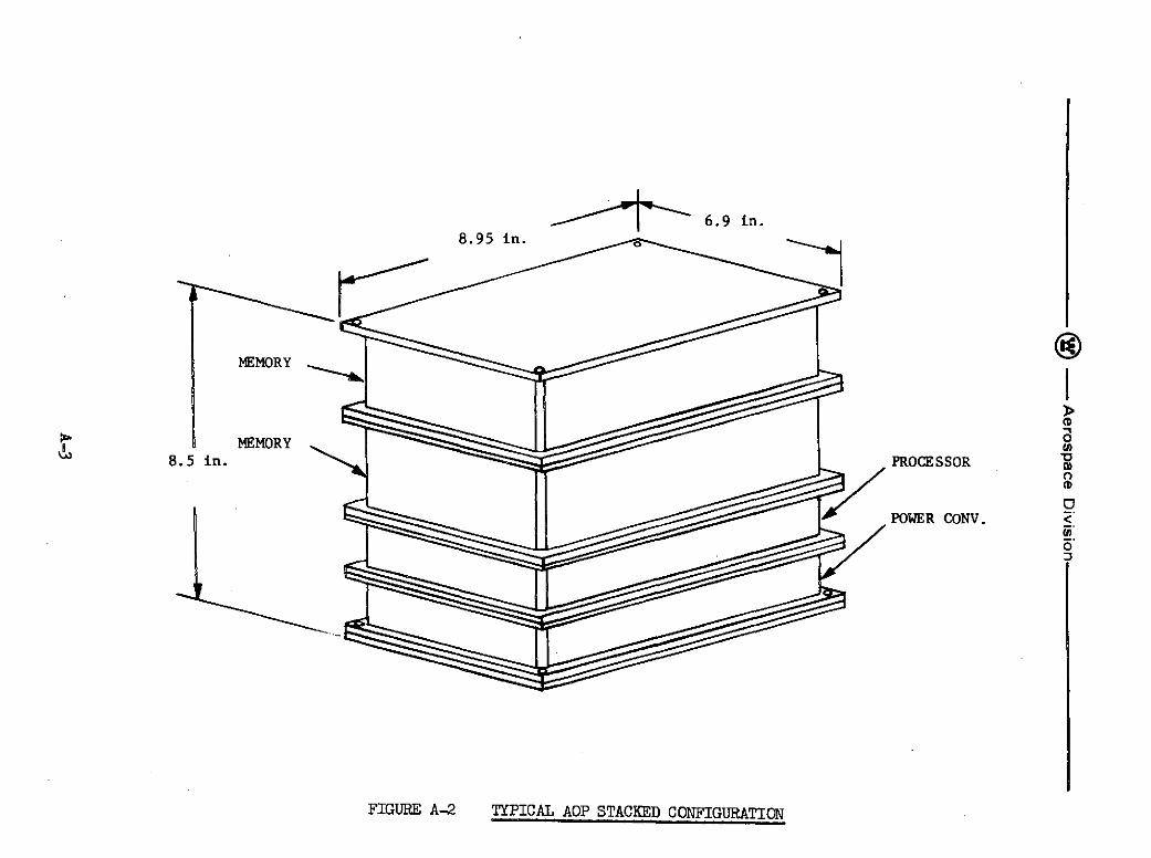
The important characteristics of the AOP are shown in table 2-1 and the
configuration of the computer, special I/O, power supply and 8K of memory is
shown in figure 2-1. The AOP is defined in detail in the attached appendix.
Logic diagrams have been delivered to GSFC and are available at that facility.
3

S--- Aerospace Division
1. WORD LENGTH - 18 Bits2. INSTRUCTION WORD - 18 Bits3. DATA FLOW - Parallel4. DATA TYPE - Fixed Point - Fraction - 2's Complement5. NO. OF INSTRUCTIONS - 556. ADD TIME - 5.0 Microseconds7. MULTIPLY TIME - 38 Microseconds8. DIVIDE TIME - 75 Microseconds9. CLOCK RATE - 800 KHz
10. NO. OF INDEX REGISTERS - One11. OPERATIONS PER SECOND - 200K12. INDIRECT ADDRESSING - Load and Store13. DOUBLE LENGTH ACCUMULATOR14. TECHNOLOGY - TTL-LSI15. SIZE - 112 cu. in. (including all I/O)16. WEIGHT - 3 pounds (including all I/O)17. POWER CONSUMPTION - Watts (CPU-Fixed I/O)18. INTERRUPTS - 16 multilevel interrupts with program lockout control
and interrupt override feature.19. DIRECT MEMORY ACCESS (DMA) - Up to 16 devices time share one channel
maximum I/O rate - 66K words per second.20. COMMAND LOAD AND DUMP-GROUND COMMAND - Control for direct memory
load or dump maximum load word rate - 300K words per second.21. MEMORY CAPABILITY - 4K modules expandable to 64K (each module in-
corporates cycle by cycle power switching).22. Direct Addressing of 4096 words in any page (addressing of all 64K
of memory is accomplished by indexing or paging).23. MEMORY WRITE PROTECTION - Storage area assigned in 128 word blocks.24. Busing Organization for parallel unpowered spare processor and/or
memory modules.
TABLE 2-1
AOP CHARACTERISTICS
4
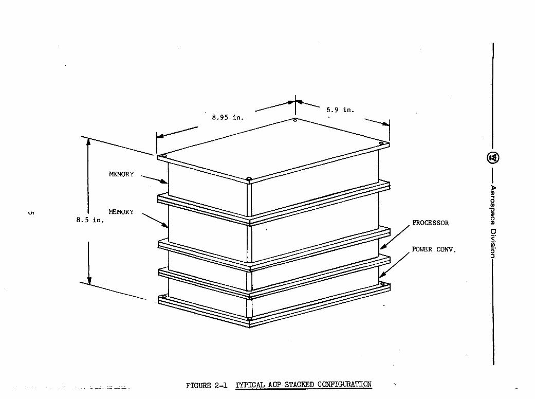
6.9 in.8.95 in.
MEMORY
MEMORY8.5 in. so i. MEORYPROCESSOR
POWER CONV.
FIGURE 2-1 TYPICAL AOP STACKED CONFIGURATION

- -- Aerospace Division
The AOP was designed especially to satisfy the requirements of all classes of
spacecraft including small satellites. In addition to practical experience
gained on the QAO-C with the OBP other systems requirements were also studied
before the design goals for the AOP were finalized. As a result the following
major design features have been achieved.
Low Power Dissipation
When operating at 100% duty cycle the power consumption is 5.0
watts including the I/O section.
" Low Volume and Weight
The volume is approximately 112 cu. inches and the weight is 3 lbs.
including the I/O section and the special I/O section.
. High Speed Arithmetic and Logic Capability
The AOP is approximately twice as fast as the OBP.
Flexible Input Output Design
Program independent data transfers are accomplished through the use
of 16 buffered I/O channels operating in a cycle steal mode, sharing
common Direct Memory Access (DMA) hardware.
Interrupt Philosophy
Sixteen individually armed priority interrupts allow asynchronous
spacecraft events to gain access to computer operation at event dependent
intervals.
* Modularity
The nominal AOP system consists of two "double ported" processor
modules and a minimum of two memory modules connected by two data buses.
Each memory is dedicated to a single data bus. The modules along with
the power supply module are packaged to provide a mechanically integrated
package. The size is expandable depending on system requirements. The
6

® -Aerospace Division
mechanical arrangement is shown in figure 2-1 and the data bus diagram
is shown in figure 2-2.
Reliability
Reliability at the component level was achieved by the following
steps:
1. Simple designs using minimum components.
2. Proven process for LSI Arrays (TTL).
3. Proven metalization process for CMMA.
4. High reliable screening during CMMA production.
System reliability depends on the mission constraints and requires
either a simplex system or dual simplex system shown in figure 2-3 (a),
or a single duplex system shown in figure 2-3 (b). The AOP uses the
single duplex system of figure 2-3 (b).
Support Software
Support software consists of an assembler, loader and simulator.
These programs are embedded in a flexible control language. The entire
system is link structured Fortran program with minimal use of assembly
language. Minimum configuration is an SDS 920.
Spac ec raft Applications
Interconnection with remote multiplexers can provide the computer
with access to all onboard data. The computer can process and/or format
data in a programmable manner which provides great flexibility to any
mission. Digital to Analog converters can provide analog signals for
control loops.
Table 2-2 is an attempt to summarize areas in which the computer can
contribute or enhance operations capability on future satellites. It
should be emphasized that this is an incomplete list and is growing
7

- Aerospace Division
BUS 'A' BUS 'B'
PROCESSOR PROCESSOR 1 ACTIVE
MODULE MODULE (PWRD UP)
MEMO MEMO
MODULE MODULE
UP TO 8
ACTIVE
ON EACH BUS
MEMaRY MEMR
MODULE MODULE
FIGURE 2-2 AOP SYSTEM BLOCK DIAGRAM
8

-- Aerospace Division
CPU4
CPU
I/O 4K
PROCESSORS MEMORIES
(a) Dual Simplex Design
CPU4KK
I/O
CPU
PROCESSORS MEMORIES
ANY 2 OF 4 MODULES MUST OPERATE
6 PCGSIBLE COMBINATIONS
(b) Single Duplex Design (AOP)
FIGURE 2-3 RELIABILITY MODELS
9

® - Aerospace Division
Command Handling
1. Storage for Delayed Executiona. Long Term Scheduleb. Special "Scratch Pad" Requests
2. Execution of Stored Sequences3. Execution of Data Dependent Commands
Data Handling
1. Format Control2. Data Compression3. Status Summary4. Operations Summary5. Limit Checking
Spacecraft Operation
1. Emergency Control Sequences2. Failure Workarounds3. Thermal Control4. Power Scheduling5. Array/Regulator Control6. Attitude Control
a. Stabilizationb. Pointing/Maneuveringc. Momentum Management
7. System Test and Diagnosis
Experiment Operation
1. Event/Data Dependent Control/Commands2. Routine Experiment Mode Control and Operation Scheduling3. Test and Diagnosis4. Sensor Stimulation and/or Calibration5. Data Processing
TABLE 2-2
LIST OF ON-BOARD COMPUTER FUNCTIONS
10

I -- Aerospace Division
everyday as new experience is gained on present day computerized
spacecraft.
3.0 AOP BREADBOARD
An AOP Breadboard was designed using small scale integrated circuits (SSI)
in DIP packages and discrete circuits to verify the functional operation of the
AOP logic.
The logic of the breadboard was partitioned in groupings representative of
the expected CMMA devices. Off the shelf Augat wire wrap boards and a wire
wrap mother board were used, each containing logic equivalent to three CMMA
devices. The completed breadboard required 23 wire wrap boards and two mother
boards of 13 slots each.
3.1 Circuits
The circuits used in the breadboard were a mix of TTL and DTL with low
powered 5L series being used as much as possible due to characteristics
similar to CMMA circuits.
3.2 Mechanical Features
The complete unit measured 19 x 9.5 x 19 inches consisting of two sub
units each mounted in a standard 19 inch rack and each measuring 19 x 9.5 x 9.5
inches.
A bracket on the back of the unit provided in addition to protection for
the wire wrap terminals a mounting location for the connectors. The two memory
connectors were mounted to this bracket, in addition two test connectors and
two I/O connectors were mounted on flexible cables. Each individual board was
divided into three sections each section containing the logic required for one
CMMA. With this approach the CMMA logic and the wiring list for the multilayer
board could be checked prior to final design. Table 3-1 shows the partitioning
11

---- Aerospace Division
TABLE 3-1
AOP BREADBOARD PARTITIONING
PARTITIONED SEGMENTS
BOARD X Y Z BOARD
POSITION CMMA # FUNCTION CMMA # FUNCTION CMMA # FUNCTION TYPE
A 17 ACC(1-3) 17 ACC(4-6) 17 ACC(7-9) 1B 17 ACC(10-12) 17 ACC(13-15)' 17 ACC(16-18) 1C 17 IM(1-3) 17 MQ(4-6) 17 MQ(7-9) 1D 17 MQ(10-12) 17 MQ(13-15 17 MQ(16-18) 1E 16 DECODE (MINOR) 14 10 2F 16 DECODE (MAJOR) 11 12 3G 4 5 25 4H 22 SPACK(O-7) 2 3 5I 22 SPACK (8-15) 6 13 6J 23 7 1 7K 15 9 8 8L 18 ADDER(1-3) 19 MOR 1-3 20 INT 0-3) 9M 18 ADDER(4-6) 19 MOR 4-6 20 INT 4-7) 9N 18 ADDER(7-9 19 MOR 7-9 20 INT 8-11) 9O 18 ADDER(10-12) 19 MOR 10-12) 20 INT 12-15) 9P 18 ADDER(13-15) 19 MOR 13-15) 20 REQ 0-3) 9Q 18 ADDER(16-18) 19 MOR(16-18) 20 REQ 4-7) 9R 19 ADR(1-3 21 BLAD 1-4) 20 REQ 8-11) 10S 19 ADR 4-6 21 BLAD 5-8) 20 REQ 12-15) 10T 19 ADR 7-9 21 BLAD(9-12) 26 LOWER LIMIT 11
Bus(13-14)U 19 ADR(10-12 21 BLAD(13-16) 26 UPPER LIMIT 11
BUS(15-16)V 19 ADR(13-15) 19 ADR(16-18) 24 CSA,SL 12
TABLE 3-1
AOP BREADBOARD PARTITIONING
PARTITIONED SEGMENTS
12

S----Aerospace Division
of the AOP Breadboard.
3.3 Test Panel and Memory
In order to check out the AOP breadboard a test panel and a 4096 word
memory was supplied to Westinghouse by GSFC. To limit interface lines all data
transfers between the AOP and the test panel were made through the memory
operand register (MOR). Only the MOR and the instruction register were displayed
on the front panel. The remaining addressable AOP registers were loaded via
the MOR and displayed on the front panel.
Both "read" and "write" operations were permitted with the test panel.
Other controls available were: initiating and master clear of AOP, clearing
the MOR, clearing and interrupt override control, operation controls. Operational
controls were available to initiate one instruction at a time, cycle on one in-
struction or go into a "run" mode to execute a complete program. Verification
was also possible in an "off line" mode of operation.
3.4 Breadboard Checkout
The checkout consisted of exercising the AOP breadboard in an "off line"
mode, 1.e., without the memory. This procedure checked out approximately 85fo
of the instructions. After verifying the unit in this manner, the memory unit
was interfaced with the AOP breadboard and full instructions were executed and
programs were loaded into the memory and executed. The diagnostic programs used
to test the AOP breadboard were developed by GSFC. During the initial checkout
of the breadboard, personnel associated with the software contractor were on
hand to aid in loading and interpretation of the programs. In addition, GSFC
personnel assisted in the initial checkout of the breadboard.
13

,, - Aerospace Division
4.0 CUSTOM METALLIZED MULTIGATE ARRAYS (CMMA)
An earlier study was conducted jointly by Westinghouse and GSFC to determine
availability of Large Scale Integrated Circuits (LSI) from which the AOP could be
fabricated. As a result of this study it was decided to take advantage of an
existing development program in another NASA facility. The circuits developed
under this program consisted of a standard chip containing 92 standard gates,
24 drivers and 24 expanders, 48 resistors and 24 diode clamps. These circuit
elements were then interconnected to provide the required logic function. Each
different logic function required its own set of custom masks. The CMMA device
is discussed in detail below.
The decision to use these circuits was based primarily on the following:
1. The least expensive 1SI arrangement available.
2. These circuits allowed maximum usage of circuits on the chip provided
the 40 pin limitation of the package was not exceeded.
3. The TTL device is inherently more radiation resistance than certain
other circuit types.
4. The speed power product is comparable to or better than other low
power circuits.
5. The power dissipation is within the desirable range for space applications.
6. Flexibility enabling the fabrication of a wide variety of logic functions.
4.1 LSI Circuit Description
The CMMA is a two level, bipolar, LSI array utilizing the transistor-
transistor logic (TTL) technique. The first layer of metalization interconnects
the bipolar devices into logic elements; 92 standard wired-or gates, 24 emitter
follower drivers, 24 three input expanders, 48 resistors and 24 diode clamps.
The second layer of metalization interconnects the logic elements into functional
14

.-- Aerospace Division
CMMA devices.
4.1.1 Die Organization
The LSI Die Organization is illustrated in Figure 4-1. This figure
presents standard columns, driver columns, extender columns and bonding pad
and scribe areas. The standard columns represent the standard or low power
gates illustrated in Figure 4-2. The driver columns represent the driver gates
and are illustrated in Figure 4-3. These are the high power driver circuits
that are used to interface with circuits on other chips or with other subsystems.
Figure 4-4 is the schematic of the circuits in the extender column. Also included
with the extender column are resistors and diode clamps. The standard gate
circuits are used only inside a given chip, while the driver is used for both
internal and external interconnections.
4.1.2 LSI Configuration
The LSI Die Organization illustrated in Figure 4-1 references the basic
arrangement of circuits available. The concept utilized on the program for
circuit fabrication, is as follows. First a simiconductor wafer, a bipolar
array, is processed as a single unit containing many die like those referenced
in Figure 4-1. In order that each of these die may become a CMMA device, an
interconnect arrangement is required. This leads to the second step. A layer
of metallization is deposited on the die which interconnects the bipolar devices
into logic elements. A total of 92 standard gates, 24 expanders, 48 resistors,
24 clamps, and 24 drivers are thus formed on each die. These are the building
blocks used to functionally implement the circuitry dictated by each drawing.
The third step deposits a second layer of metallization to interconnect the
logic elements available after the first layer of metallization has been com-
pleted. This step creates a Custom Metallized Multigate Function.
15

S- Aerospace Division
STANDARD DRIVER GATE EXTENDER BONDING PADCOLUMNS COLUMN COLUMN & SCRIBE AREA
FIGURE 4-1
MA DIE ORGANIZATION
16

® - Aerospace Division
VcVCC
R1
1 T2 OUT
T3
R1 = 30.4 K
R2 = 2.53 K
R3 = 20.8 K
FIGURE 4-2
STANDARD GATE
17

S- Aerospace- Division
V00
T
RT 4
R= 16.9 K
R = 1.41
3 = 8.4 K
R = 10.8 K
FIGURE 4-3
DRIVER GATE
18

-Aerospace Division
Vc0
i \R1/5
=I- 30.4 K
R2 = 2.53 K
FIGURE 4-4
EXTENDER/PULL-UP CELL
19

-- Aerospace Division
a. STANDARD GATE2. 4V
b. DRIVER GATE
GATE
GENERATOR
C
b. DRIVER GATE
2 1. V V
OUTNUT
GATE
PULSEFIGURETEST
GENERATOR
PROPAGATIONVOLTAGE WAVEFORDELAY ASUREMENT SETUP
1.1V 1.1 V
pdO pdl
OUTPUT VOUT (1)1.1V 1.1V
-OUT' '
FIGURE 4-5
PROPAGATION DELAY MEASUREMENT SETUP
20
® -- Aerospace Division
A via layer or communication layer enabling a larger number of interconnects by
passing signals from the first layer to second layer was also assiciated with
the second layer metallization.
4.2 Circuit Layout
The object in designing a system is to partition the logic so that one LSI
circuit type can be used for a number of different applications in the system
design. In the developed AOP Processor, 27 types and a total of 69 LSI circuits
were required.
4.3 CMMA Layout
Westinghouse experience shows that layout problems increase in a nollinear
manner as 100%o utilization of logic elements on the die is approached. Also
certain circuit configurations requiring complicated interconnects proved dif-
ficult.
4.4 Testing
Westinghouse generated two sets of test documents to verify the CMMA cir-
cuits. A set of static tests to verify the chip parameters and the logic inter-
connect. A set of dynamic tests to verify propagation delays and final circuit
characterization.
Each chip was probed with forty tips, one for each input/output pad and
the static tests cycle was executed. The chip having passed visual prior to
static tests was packaged in a forty pin flat pack, given 96 hour burn-in at
12500C. The unit then went through static and dynamic tests before delivery.
4.5 Equation Development and Specifications
In order to design the computer the limitations of the circuits and oper-
ating parameter must be well defined. This data was suppled to Westinghouse by
the Semiconductor Manufacturer and is shown in tables 4-1, 4-2 and 4-3.
21

S---Aerospace Division
N = Fan-Out (Loading)
M = Additional Outputs Added' as Wired-Or Configuration.
E = Expanders (Increase Number of Inputs)
R = Additional Pullup Resistors
12 MT = 20 + .22 RL C +-12 Mpdl 1R N +R
30= N +R
C1 = 3 + N + R
Tpd0 = 60 + 10 (E - R) R 4 E
Delay (N - 0-10)
Tpdl TpdO
a) Fan-Out (N) Per Tpdl Equation 60 NSEC MAX(Open Collector)
b) Wired-Or Per T Equation 60 NSEC MAX(Additional Outputs)
c) Pullup - No Clamp Per TpdI Equation 160 NSEC MAX(Off Chip Drive)
d) Expanders Per Tpdl Equation Per TpdO Equation
TABLE 4-1
STANDARD GATE SPECIFICATIONS (ORIGINAL)
22

S----Aerospace Division
N = Fan Out (Loading)
M = Additional Outputs or Wired-Or Configuration
E = Expanders (Increase Number of Inputs)
R = Additional Pullup Resistor
T 35 + 100 [() (M + 1) + N +pd N (11) + (M +1) (30) 1
C1 = 20
Tpd0 = 40 + 10 (E - R)
Delay (N = 0-50)
Tpdl TpdO
a) Fanout 40 NSEC MAX 40 NSEC MAX
b) Wired-Or Per T dl Equation 40 NSEC MAX(Additional Outputs)
c) Expanders 40 NSEC MAX Per Tpd 0 Equation
TABLE 4-2
DRIVER GATE SPECIFICATIONS (ORIGINAL)
23

S---Aerospace Division
STANDARD GATE
Levels Logic "1" 2.4 - 5.OV (Output) 2.0 - 5.5V (Input)
Levels Logic "0" 0.0 - 0.3V (Output) 0.0 - 0.7V (Input)
Loading Input Load 1 Unit Load
Output Drive 10 Unit Loads
Speed
TpdO 60 nsec Max (n = 1-10)
Tpdl Per Tpd Equation
Current (Input) .26 ma (-350C) .18 ma (2500C) 0.135 ma (1000C)
Power "l" 1.3 1.0 0.77 mw
Power "O0" 0.95 0.78 0.71 mw
DRIVER GATE
Levels Logic "l" 2.4 - 5.OV (Output) 2.0 - 5.OV (Input)
Levels Logic "O" 0.0 - 0.3V (Output) 0.0 - 0.7V (Input)
Loading Input Load 1.8 Unit Loads
Output Drive 50 Unit Loads
Speed
TpdO 40 nsec Max
Tpdl 40 nsec Max
Current .47 ma (-350C) .32 ma (2500C) .25 ma (1000C)
Power "l" 2.5 1.8 1.3 mw
Power "O" 5.2 4. 0 3.0 mw
TABLE 4-3
CIRCUIT SPECIFICATION TEMPERATURE RANGE -350C to +1000C (ORIGINAL)
24

1 - Aerospace Division
The ground rule for this data is that a standard gate or driver gate must
be clamped with the circuit of figure 4-4 when: four wired "OR" structures
are connected to one point or when interfacing with another chip.
These equations and parameters were used in the initial design of the AOP.
Subsequently the equations and parameters were modified by the Semiconductor
Manufacturer.
4.6 Circuit Characterization
Tables 4-1 and 4-2 refer to equations which define the delays of the
standard gate and driver gate. It was very simple to determine the operating
conditions of a single gate or driver and thus calculate the specifications but
much more difficult to calculate the specifications for a logic chain. It
was decided that maximum values could be determined for certain gate combinations.
These values were then applied to logic chains which specified a worst case
condition.
4.7 Final Circuit Development
In some cases the initial specifications for the circuits and the charac-
terization of the circuits proved to be more stringent than the subcontractor
was able to comply with. Changes to the specifications were necessary as the
program developed.
4.8 Generation of New Equations
During the program revisions were made to the equations given in tables
4-1 and 4-2 and to the specifications in table 4-3.
In the equation for Tpdl, the constant 0.22 was changed to 0.304. When
this constant was established the forward drop across the diode VBE was neglected.
Assuming the following values,
25

® - Aerospace Division
ETH - 1.1 volts Eo VCC VBE
VBE = 0.8 volts
E = EO (1 -E - t/RC)
t = 0. 3 04 RL CT R = Total Load CT = Total Capacitance
The method of evaluating the capacitance and resistive loads was changed. The
capacitive loading on a standard gate output was increased 3 pf for each OFF
gate whose outputs were connected to other inputs of the driver gate. Another
1 pf was added for each gate input tied to the OFF gate output. If the OFF
gates is the emitter follwer type or a resistor pull up is present, no additional
capacitance is added.
The value of R is not increased by an OFF gate in the fan-out. The
constant 30 in RL N +R is changed to 39. The final circuit equations areN + R
shown in table 4-4 and the final parameters are shown in table 4-5. Devices
were delivered to Westinghouse according to these specifications. The power
dissipation shown in table 4-5 and in table 4-3 is given for high resistance
material. Both low and high resistance material was delivered to Westinghouse.
The power dissipation of low resistance material should be increased by 30%
over the values given in the tables.
5.0 CMMA BREADBOARD
To facilitate testing the CMMA circuits before mounting them on the multi-
layer board, Westinghouse fabricated a CMMA breadboard. It was determined that
a breadboard test unit was an essential piece of equipment for testing the
chips and evaluating AOP system performance prior to final assembly of the
system. The following list of needs and uses for the breadboard supported
the decision to build it.
26

® - Aerospace Division
STANDARD GATE
Tpd = 20 + .304 R C1 + 12M where R = -9pdl N + Re N +R
TpdO = 6 0 nsec (N - 1-5) C = 3 + N +R
TpdO = 100 nsec (N = 6 - 10)
TpdO = 6O + 10 (E - R) (N =1-5) Where Applicable
Tpd = 100 +10 (E -R) (N = 6-10)
DRIVER GATE
Tpdl = 50 nsec (N = 1-50)
TpdO = 50 nsec (N = 1-50)1OO
T 35 00 (5(M +1) + N +pdl = 35 +N(11) + (M + 1) (30) 1 )Where Applicable
T pd = 50 + 10 (E - R)
TABLE 4-4
REVISED EQUATIONS
27
- Aerospace Division
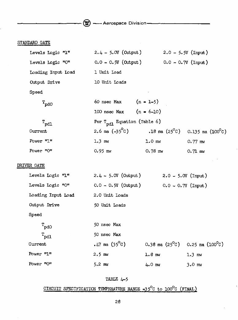
STANDARD GATE
Levels Logic "l" 2.4 - 5.0V (Output) 2.0 - 5.5V (Input)
Levels Logic "O" 0.0 - 0.5V (Output) 0.0 - 0.7V (Input)
Loading Input Load 1 Unit Load
Output Drive 10 Unit Loads
Speed
TpdO 60 nsec Max (n = 1-5)
100 nsec Max (n = 6-10)
Tpdl Per Tpd I Equation (Table 6)
Current 2.6 ma (-350C) .18 ma (250C) 0.135 ma (1000C)
Power "l1" 1.3 mw 1.0 mw 0.77 mw
Power "0" 0.95 mw 0. 78 mw 0.71 mw
DRIVER GATE
Levels Logic "l" 2.4 - 5.OV (Output) 2.0 - 5.OV (Input)
Levels Logic "O" 0.0 - 0.5V (Output) 0.0 - 0.7V (Input)
Loading Input Load 2.0 Unit Loads
Output Drive 50 Unit Loads
Speed
TpdO 50 nsec Max
TpdI 50 nsec Max
Current .47 ma (3500C) 0.38 ma (2500) 0.25 ma (10000C)
Power "l" 2.5 mw 1.8 mw 1.3 mw
Power "0" 5.2 mw 4.0 mw 3.0 mw
TABLE 4-5
CIRCUIT SPECIFICATION TEMPERATURE RANGE =35o0C to 1000 C (FINAL)
28
S-Aerospace Division
1. The program schedule called for the delivery of the last CMMA chips
before final delivery of the multilayer board. The CMMA breadboard
allowed system testing without the PC board and consequently made it
possible to deliver the system earlier.
2. Troubleshooting was much easier when questionable chips could be
changed without soldering or cutting leads.
3. Any changes required to the multilayer board could be made before the
chips were mounted, thus avoiding exposure of the circuits to excessive
handling.
4. Verification of the wiring list used to layout the multilayer board,
therefore, all corrections to the board could be made prior to the
assembly of the engineering model.
5. The interfaces between the AOP-CPU, plated wire memory, and special
I/O could be tested and debugged prior to final assembly of the system.
6. The circuits could be tested for both correct functional operation
and speed.
7. Any new system problems arising from the use of CMMA devices could be
determined and necessary design changes could be easily evaluated.
In practice the breadboard proved to be an invaluable piece of equipment
without which it would have been extremely difficult if not impossible to debug
the system in the time allocated.
5.1 Fabrication
The fabrication technique of the CMMA breadboard was influenced by the
availability of parts and time required for assembly which led to the selection
of a dual bucket assembly with a wire wrap back panel similar to the original
breadboard. Westinghouse designed a double sided printed circuit board which
29

@ - Aerospace Division
plugged into the buckets and on which contactors were mounted. These contactors
were used to hold the CMMA circuits.
5.1.1 Contactors
The contactors for the CMMA breadboard were selected after observing the
test set used at the subcontractor's facility. The CMMA circuits were packaged
in the 50 mil lead packages and then placed in a 50 pin plastic carrier by the
subcontractor. The circuits were left in the carriers for test and shipment
to Westinghouse. The subcontractor also utilized a 50 pin contactor to firmly
hold the 50 pin plastic carriers and at the same time make electrical contact
with the leads of the CMMA package. The contactor contained 50 pins which
extended from the bottom and were used to make electrical connections with the
outside world. A solid metal latch pivoted on one end of the top of the contactor
and was used to secure the plastic carrier and in turn force the package leads
onto the contactor pins without damaging the leads of the package.
Utilizing these contactors, Westinghouse was able to insert the circuit,
as delivered by the subcontractor into the system for test purposes. Any
package could be placed in any contactor, facilitating the system checkout.
5.1.2 Printed Circuit Board
After selecting the contactor for the CMMA breadboard a board and bucket
arrangement similar to the original breadboard was used to efficiently package
the CMMA breadboard. The boards used for this purpose were designed by
Westinghouse and were capable of holding three contactors and 120 output pins
making them identical at the interface with the original breadboard. The
board edge was plated and utilized as an edge connector to mate with the back
panel mother plate. Since 66 circuits were utilized in the original system,
and eventually increased to 69, 23 boards were required to implement the design.
As the design and test progressed, an additional board was added, for
30

S - Aerospace Division
the additional type 27 circuit.
5.1.3 Board Rack and Back Panel
Two racks, each capable of holding thirteen boards (identical to the racks
used for the first breadboard) were used to mount the printed circuit boards
and provide a wire wrap back panel for interconnecting the boards. Twenty-
three of the twenty-six available 120 pin connectors were used for intercon-
necting the CMMA circuits. All wires to the test panel, memory, or special
I/O were routed to the remaining three connectors to provide a localized area
for interface signals. The connectors for interface cables were mounted on a
panel at the back of the unit as in the original breadboard and the back panel
was automatically wire wrapped.
5.1.4 Wiring List
The goal in the generation of the wire list was to generate one list for
both CMMA breadboard and the engineering Model AOP. The wiring list for the
back panel was designed so that each 120 pin connector was sub-divided into
three forty pin sections. Within the forty pin sections the pin numbers were
assigned identical to the CMMA package pin numbers. This made it possible to
generate a breadboard wire list similar to the engineering model wiring list
automatically with a special computer program. This feature also facilitated
the breadboard checkout. The leading item in the wire list generation was the
"pin out" information generated by the subcontractor. Westinghouse had the
wire list program avialable long before pin out data was available.
5.2 Testing
When the CMMA breadboard had successfully completed all the tests that
could be practically performed at Westinghouse, it was taken to NASA GSFC for
further testing to verify the AOP plated wire memory, the diagnostic tests and
the AOP I/O. The advantages of performing these tests while the AOP was still
31

S- Aerospace Division
in breadboard form include the following:
1. The residual spare chips to be delivered to GSFC at the termination
of the contract could be conveniently tested.
2. The speed of the system could be measured, critical paths determined,
and any design changes to improve performance could be easily imple-
mented and evaluated.
3. GSFC system integration between the CPU, Memory, I/O and software
could be performed at an earlier date than would otherwise have been
possible.
The tests performed at GSFC with the aid of the computer system and I/O
were more exhaustive than those conducted at Westinghouse. It was practical
to load much longer and more comprehensive diagnostic programs through the I/0,
under computer control. Memory contents could be examined and compared with
the program originally loaded to diagnose failure quickly. Interrupts, I/O
cycle steal operations and CPU programs were run concurrently over a wide
range of I/O rates to thoroughly exercise the memory control hardware.
6.0 ENGINEERING MODEL AOP
The engineering model AOP was designed and fabricated to resemble, as
closely as possible, a flight quality processor. The AOP was designed utilizing
the latest multilayer board technology, an ISI circuit technology and a com-
pressed packaging arrangement. The AOP consists of a chassis with a volume
of 112 cubic inches, containing four cutouts for four 100 pin Deutsch connectors,
mounting positions for the AOP multilayer P.C. Board and the special I/O
Board. The design also included an eighteen layer multilayer board, 69 CMMA
circuits, a special I/O mating connector and two capacitors (one to stretch
MINIT -320pf and one to delay the IRSCLK -680 pf). The chassis is referenced
by drawing IRD 2857 and the board layout by drawings RDD001-A and RDDO01-J.
32

S-- Aerospace Division
6.1 CMMA Package
Section 4 discusses the CMMA circuit technology and development concept.
The basic CMMA circuit consists of a bare chip approximately 150 mil x 175 mil
which, in the AOP program, was to be packaged in one of two 40 pin packages.
The basic package configuration was that of a circular flat pack approximately
- inch in diameter with twenty leads extending from opposite sides. Figure 6-1
illustrates the package and associated markings. The packages used in the
system were supplied by Sprague and the larger and smaller units had part
numbers FH115 and FHO80 respectively. The difference in the two packages were
in the lead dimensions only; the FH80 package was organized with 35 mil center
to center spacing in the leads. The overall package size is approximately 1.0
inches by .7 inches. The larger package (FHll5) was designed with 50 mil center
to center lead spacing. The overall package size is approximately 1.4 inches
by 1.0 inches.
Originally, the FH80 package appeared to be the most desirable from a
size and therefore packaging standpoint, the overall dimensions of this package
would allow for a more dense packaging approach and a smaller multilayer
board. While these packages appeared desirable from a packaging standpoint,
other factors indicated the larger package was more desirable for a development
type program. First, the subcontractor was utilizing the FH115 package in the
pre-development phase and these packages were available at his facility.
Secondly, the subcontractor's test jigs and other fabrication setups were
organized around the larger package and therefore it would be more expensive
to use the smaller package. Thirdly, many of the layout facilities available
for multilayer board layouts were organized on divisions of 100 mil center,
1.e. 50 mil centers were quite desirable. Finally, both the ease in the
initial soldering and the capability of removing CMMA circuits from the solder
33

S -- Aerospace Division
Hs-151W
XXX: DATE CODE
YY: CIRCUIT NUMBER
QUANTITY:
FIGURE 6-1
CMMA PACKAGE
34

I@ -- Aerospace Division
pads dictated the use of the larger package. The final system required 69
of the CMMA packages to implement the AOP design.
6.2 Multilayer Board Fabrication
The design for the AOP included the latest multilayer board (MLB) tech-
nique, with a design goal to mount the CMMA circuits on one multilayer board,
utilizing both sides of the MLB. The acceptable maximum was to use two (2)
MLB's in the construction of the AOP in order to package the CMMA circuits.
6.2.1 Multilayer Board Types
Two available techniques for multilayer board constrction were considered
acceptable, the post build up technique and the plated-through-hole technique.
Both techniques require artwork to define the printed circuit wiring for the
various layers and the hole layout.
The post build up technique was being evaluated by GSFC under a separate
contract for the AOP as well as other programs. The company supplying GSFC
with these boards discontinued their efforts in this area; therefore,
Westinghouse chose the plated-through-hole technique for the AOP multilayer
board. The plated-through-hole technique had been widely used in industry
and was considered a reliable packaging and wiring technique.
The fact that each CMMA package contained 40 pins required that 40 holes
must be drilled through the board, and with CMMA's mounted on both sides, 80
holes per square inch were necessary. This density of drilled holes is con-
sidered to be the main disadvantage of the plated-through-hole type multilayer
board. The hole area and associated clearances consumed much of the printed
circuit area, thus requiring additional layers to complete the assembly.
6.2.2 Multilayer Board Configuration
The multilayer board configuration was controlled by two factors, the
35

- Aerospace Division
available area for the board and the number of circuits to be packaged. As
previously stated, it was possible to use two multilayer boards for the AOP;
but this was not the design goal. After several layouts and consultations
with GSFC, the final board configuration for the system was selected. One
board contained 35 circuit positions on either side in a rectangular 5 x 7
array. One edge of the board contained the lower and upper bus connector
areas while the other edge of the board contained the test panel and I/O
connector areas, the short dimension of the board contained a connector area
for the special I/O board in case it should be mounted inside the AOP chassis.
This board size dictated that the chassis size be increased to 8.95 inches
by 6.9 inches, exceeding the outline of the memory unit.
The packages were evaluated and it was decided a 1" x 1" area would be
sufficient to package one CMMA circuit, requiring the leads to be cut to
approximately .25 inches max. in the center.
The design and assembly of the multilayer board included a connector
area in which a 70 pin connector was mounted. This connector was to be used
at some later date to test out various special I/O designs that might be
required for system applications. The basic board layout is illustrated in
the layout drawings for the AOP, RDD001-A and RDD001-J. All chip types and
the associated AOP functions are included. Connector hole areas are also
shown on these drawings. The basic board layout become a 5" x 7" area with
circuits on both sides and the remaining area was to be used for connectors,
holes and individual components. One spare position E2 exists on the multi-
layer board with no connection to any of the forty pins. Position E3 was
originally a spare postion but an additional type #27 circuit was included in
the design when incorporating changes to improve system speed.
36
) -- Aerospace tivision
6.2.3 Multilayer Board Artwork
The fabrication of the multilayer board (MLB) was initiated with the
generation of artwork which defined the hole pattern and printed circuit lay-
out for the MLB. This artwork was used as a mask in the etching process which
defined the various layers of the MLB.
The artwork for the AOP MLB was generated by computer from a program
designed for this purpose. Westinghouse generated a wire list which totally
defined the interconnect structure between the CMMA pins and the connector
areas defined on the MLB layout drawings.
The original goal was to limit the number of layers to a total of 14
including a power and ground plane. An initial evaluation by the company
generating the artwork indicated that at least sixteen layers would be required
to assemble the MLB. The final configuration required 18 layers and the fol-
lowing set of ground rules:
1. The computer program must be given complete freedom in the posit-
ioning of the circuits on the board.
2. The computer program must have complete freedom in assigning signal
names to the hole positions within each connector area.
3. The 5 x 7 circuit array would be shifted in the long dimensions so
that there would be an area for holes between every two rows of
circuits if necessary.
4. The top and bottom layers would be used for printed circuit wiring
as required by the computer program.
6.3 AOP Chassis
The AOP chassis was to be identical, in perimeter, including mounting
holes, to the plated wire memory developed for the AOP system. The original
outline was a rectangular configuration with dimensions of 8.95 inches by
37

@ -- Aerospace Division
5.85 inches. In each corner of the unit were two holes, one for a retaining
rod and one utilized to mount a similar unit on top. The basic premise behind
the AOP system design was to "stack" memories and processors to form a finished
system.
With the design of the AOP reaching a final stage, it was known that 66
to 70 circuits would be required for the AOP design. In order to package
these circuits within the confines of the dimensions specified by the plated
wire memory, five separate layouts were undertaken for the multilayer board.
The net result of this effort was an undesirable packaging arrangement, finally,
the dimensions for the multilayer board were expanded to approximately 7.9 x
5.9 inches.
The initial design of the chassis included variations of reversing the
mounting flange on one side and then both sides of the chassis. After a num-
ber of different configurations were generated, it was decided to increase the
overall dimension of the chassis with the form factor similar to the plated
wire memory chassis. This decision resulted in the AOP chassis increasing to
8.95 inches by 6.90 inches. With the 8.95 inch dimensions being maintained,
the plated wire memory could be mounted on the AOP for system tests. Any
additional plated wire memories were to have their form factor modified to
coincide with the dimensions of the AOP. The two long sides of the AOP unit
were utilized to mount four -100 pin Deutsch connectors. The "lower bus"
connector and the "test panel" connector were assembled with the unit. The
position for the "upper bus" connector was left vacant so that GSFC could
mount a 100 pin connector that would mate with t h e special I/O board as a
lower bus connector. The additional connector position was for a future I/O
interface connector.
The AOP chassis is approximately 1 3/4 inches in height, designed so that
38

( -- Aerospace Division
two multilayer boards could be mounted in the unit. The board positions
were located on the top and bottom area of the chassis with the center area
between the boards allocated for the connectors and the associated wiring.
With the Westinghouse effort resulting in only one multilayer board required
for the system design, the additional position could be utilized by GSFC for
their special I/O boards. To facilitate this arrangement, Westinghouse included
the special I/O connector area on the MLB when the artwork was being generated.
It is feasible to reduce the overall height and thus the volume of the
AOP by either selecting different connectors, and/or extending the connectors
beyond the board area. In both cases the height of the chassis could be
reduced since the total height required for the two boards is much less than
the 1 3/4 inches allocated for the chassis height. Drawing IRD 2857 references
the AOP chassis.
6.4 Assembly
After checkout of the CMMA breadboard at GSFC the unit was returned to
Westinghouse and the CMMA circuits were removed and readied for mounting.
6.4.1 Multilayer Board Changes
The tests conducted at GSFC on the AOP resulted in the addition of a
second type 27 circuit to the final design as an aid in achieving the desired
results.
The speed evaluation to determine methods of increasing speed resulted in
the following changes to the multilayer board. These changes consisted of
cutting the printed circuit wiring on the board to free the circuit lead pad
from the remaining multilayer board wiring. The circuits were then soldered
to the board and wires were soldered to the top of circuit leads. These wires
were then attached to the desired leads on other circuits. If plated-through-
holes were available they were utilized to attach the wires to the board.
39
S---Aerospace Division
Table 6-1 illustrates the changes incorporated on the multilayer board to im-
prove the system speed.
6.4.2 CMMA Circuit Assembly
The CMMA circuits were mounted on the multilayer board by parallel gap
soldering techniques which were currently in use on another space program at
Westinghouse.
The leads are first bent in a 1" bending tool, cut to the proper length,
tinned and soldered to the multilayer board with a parallel gap weld/solder
machine.
Following the circuit mounting, all standoffs, connectors and connector
wiring were mounted on the multilayer board. In order to reduce possible noise
on the voltage bus, four bypass capacitors were mounted on the board, two on
the unused upper bus connector area and two in the area below the I/O connector
opening in the chassis.
Since the plated-through-holes were located directly under each CMMA
package, a mrlar insulating strip was cut and was adhered to the bottom of
each circuit. This insulating layer completely isolated the package from the
holes. This technique is common practice on several Westinghouse space
programs.
6.5 Tests
After the initial tests were conducted on the CMMA circuits the AOP was
completely assembled and "OFF LINE" tests were conducted on the unit with the
results being very favorable.
All initial tests were conducted on the AOP unit with the diode clamp and
10K resistor pullup connected to the set lines associated with the MOR set
inputs. The tests conducted were successfully executed within a seven micro-
second "ADD" time, in fact, the unit performed the diagnostic tests supplied
40

® -- Aerospace Division
REFERENCE SIGNAL SIGNAL NAME MODIFICATION
IRSCLK IRSCLK Remove pad from DO6/30IRSCLK Add wire from E06/11 to D06/15DISPLD- Add wire from DO6/35 to D06/16DISPLD- Add wire from D06/16 to D06/17IRSCLOCK Add wire from D06/19 to J06/24
AIRCLK ,SYNC Remove pad from DO06/10OPROC Add wire from 106/22 to DO6/10
PAGE ,5YNC Remove pad from C07/91SGYNC Remove pad from G07/9
0PROC Add wire from D06/33 to C07/9ZPROC Add wire from CO7/9 to G07/9
PAGE ADR ADRCLK Add wire from A0 4/30 to A05/30Add wire from A01/30 to E03/30
ADRCLK- Add wire from E03/29 to EO1/6
MORCLK MORCLK Add wire from F06/4 to E03/3MORCLOCK Add wire from EO3/4 to A03/6
OUTTO OUTTO- Add wire from EO/12 to E03/31OUTTO Add wire from E03/32 to E07/6
#27 GND Add wire from E03/20 to GND (E03/20)5 volts Add wire from E03/40 to KOO/11
TABLE 6-1
MULTILAYER BOARD WIRING CHANGES
41

® - Aerospace Division
by GSFC with an ADD time approximately 5.5 microseconds. The major difficulties
encountered were with the limits specified for the "readcomplete" signal,
350 +100 microsecond. This dictated the machine must operate successfully over
the temperature range with a 250 microsecond readcomplete pulse and tests con-
ducted indicated this was not feasible mode of operation.
The unit properly functioned over the temperature range with the 500 micro-
second "readcomplete" pulse generated by the GFE memory with the pullup re-
moved. The ADD time did not exceed 6 microseconds over the full temperature
range. Since the arrival of "readcomplete" had been delayed to 750 +50
microseconds no problems were encountered in this area.
42

® - Aerospace Division
APPENDIX
ADVANCED ONBOARD PROCESSR (AOP)
Description and Instruction Set
43

A -Aerospace Division
AOP SYSTEM DESIGN
1.0 INTRODUCTION
The Advanced Onboard Processor (AOP) is a small, lightweight, low power,
stored program digital computer intended for onboard spacecraft applications.
It achieves its power and size objectives through the use of low power large
scale integrated (LSI) circuit technology, multilayer board techniques, and
a low power plated wire memory. The AOP evolved from an earlier model, the
Onboard Processor (OBP), which was developed jointly by Westinghouse and NASA/
GSFC as a general purpose processor on earth orbiting satellites. The develop-
ment of the AOP resulted in a reduction in size, weight, and power consumption
compared to the OBP. Figure A-1 illustrates the AOP unit.
The AOP processor module contains both a powerful CPU and a flexible I/O
unit requiring only a memory unit and power supply unit to form a complete
general purpose computer system. Figure A-2 represents the stacked arrange-
ment representing the final system configuration. The CPU, the control for
interrupts and I/O direct memory access (DMA) channels and the memory bus
controller are packaged as one unit (one board). The remainder of the I/O,
being that section of the I/O which is application dependent, is packaged
separately (one board) but within the same physical module. Figure A-3 is a
representative block diagram of the AOP - CPU. I/O units in general are re-
quired to change from mission to mission to provide different functions,
interfaces, data rates, etc. However, much of the I/O system, namely that
part which interfaces directly with the CPU and memory, tends to remain
unchanged no matter how the application requirements vary. Greater flexibility
was acheived and a wider variety of applications were served when the section
of the I/O which must be continually modified was minimized and segregated
A-1

S- A
erospace
Division
r4
This
page is
reproduced at
theback of the Teport by a
differentreproduction
method
to provide
better detail.
A-2
6.9 in.8.95 in.
MEMORY
MEMORY8.5 in. PROCESSOR
POWER CONV.
FIGURE A-2 TYPICAL AOP STACKED CONFIGURATION

FOLDOUTJ FRAME
MEMORY IMPUT BUSIBA) BIa D
________ ~~~~~MEMORXOU-TPU-T BS(Mo)IR ____________________________
________ MEMOP-,' ADDIRESS BUS (MAnt) J(,E2
vU
B~.ccE LEHGTNCYCLE STEAl. NTUTO ,ESMMR
SPECIAPL
co AN OU0-tOILE EuS U ONR . PRTROOo0 ARYOEK.VPt
5 -r P P4E S--AA-'s 5-ArO (L SR
m A\ SSY,
I/o ACE -S PACK CII.) CYCL E SA N A I L . R O A A -A
C-f LE LAOA A OPU 'Lr-I CoUtRE
BNEAV. NUNTH- ON7EVP NA NJob2e*R
6l- - 4. 3AC 2i YL 7 A -CL (117

1 ACTIVE PROCESSOR UP TO 8 ACTIVE(POWERED UP) MEMORIES ON EACH BUS
PROCESSOR MEMORY MEMORYMODULE MODULE MODUIE
BUS "A"
0BUS "B"
PROCESSOR MEMORY MEMORYMODULE MODULE MODULE
FIGURE A-4 AOP SYSTEM CONFIGURATION

® -- Aerospace Division
1. WORD LENGTH - 18 Bits2. INSTRUCTION WORD - 18 Bits3. DATA FLOW - Parallel4. DATA TYPE - Fixed Point - Fractional - 2's Complement5. NO. OF INSTRUCTIONS - 556. ADD TIME - 5.0 Microseconds7. MULTIPLY TIME - 38 Microseconds8. DIVIDE TIME - 75 Microseconds9. CLOCK RATE - 800 KHz
10. NO. OF INDEX REGISTERS - One11. OPERATIONS PER SECOND - 200K12. INDIRECT ADDRESSING - Load and Store13. DOUBLE LENGTH ACCUMULATOR14. TECHNOLOGY - TTL-LSI15. SIZE - 112 cu. in. (including all I/O)16. WEIGHT - 3 pounds (including all I/O)17. POWER CONSUMPTION - 5 Watts (CPU-Fixed I/O)18. INTERRUPTS - 16 multilevel interrupts with program lockout control
and interrupt override feature.19. DIRECT MEMORY ACCESS (DMA) - Up to 16 devices time share one channel
maximum I/O rate - 66K words per second.20. COMMAND LOAD AND DUMP-GROUND COMMAND - Control for direct memory
load or dump maximum load word rate - 300K words per second.21. MEMORY CAPABILITY - 4K modules expandable to 64K (each module in-
corporates cycle by cycle power switching).22. Direct Addressing of 4096 words in any page (addressing of all 64K
of memory is accomplished by indexing or paging).23. MEMORY WRITE PROTECTION - Storage area assigned in 128 word blocks.24. Busing Organization for parallel unpowered spare processor and/or
memory modules.
TABLE A-1
AOP CHARACTERISTICS
A-6

S-- Aerospace Division
from the rest of the system. At the same time, the I/O DMA channels were re-
designed to permit a reduction in the hardware required to implement them.
Table A-i specifies the AOP characteristics.
To meet the stringent reliability requirements of space hardware the AOF
was designed utilizing a dual bus concept. In operation, at least two 4096
word memory modules would be used, one connected to each bus. All data, address
and control lines for the memories are duplicated so that in the event of a
failure in one bus, the remaining memory can be programmed and the mission can
continue although possibly in a degraded mode. As many as eight memory modules
may be connected to each bus. In addition, an unpowered standby processor
module may be connected to both buses without affecting the operations of the
powered processor. Figure A-4 illustrates an AOP system busing organization.
The circuit technology selected for the AOP was that of a custom metal-
lized multigate array (CMMA) LSI circuits containing an array of 116 three
input NAND gates and 24 three-input expanders which may basically be connected
in any manner. The gates are divided into two groups; 92 low power open col-
lector standard gates which are used to drive inputs on the same chip, and 24
high power active pullup driver gates used to drive inputs on other chips or
outside the processor module. The driver gates may be connected in such a
way as to convert them to open collector output devices for such uses as
memory bus drivers where the "wired-or" function is necessary. The processor
is partitioned into 69 CMMA circuits of 27 unique types. The circuits are
mounted in circular 40-pin flat packages which are mounted on both sides of a
single 18-layer multilayer board. The board is mounted in an aluminum chassis
8.95 x 6.90 x 1.76 with space allocated for one other board containing the SIO
circuitry.
A-7

S---Aerospace Division
2.0 CPU OPERATION
The AOP CPU is a fractional, two's complement fixed point computer. The
word length is 18 bits. All logical and arithmetic operations and register
transfers are fully parallel. There are four directly addressable registers
and two additional registers which can be addressed via special instructions.
2.1 REGISTERS
An 18 bit accumulator (ACC) is used as one operand in most arithmetic and
logical instructions and also stores the result of these operations. It's
contents may also be tested for odd parity, compared to memory contents, com-
plemented, negated, tested for sign and reversed.
The 18-bit memory operand register (MOR) is a storage register for all
data being transferred to and from memory. It also serves as the other
operand in arithmetic and logical operations and acts as temporary storage
during register exchanges.
An 18-bit address register (ADR) stores the effective address for all
memory accesses in its least significant 16-bits. It may be loaded from the
MOR, the adder, and the page register. Also a four-bit block code specifying
a particular 4096 word block of memory may be loaded into the ADR from the SIO
during an Interrupt, and EXIT or RESUME instruction.
An 18-bit extended accumulator or multiplier-quotient register (MQ) may
be loaded from and stored into memory. It holds the least significant half
of the divisor and the entire 18-bit quotient during a DIVIDE instruction.
It may be shifted with the accumulator during DOUBLE SHIFT, DOUBLE CYCLE and
NORMALIZED instructions. It retains the least significant half of the product
in the MULTIPLY instruction.
An 18-bit index register (IDX) may be added to the ADR to form the effective
A-8

( - Aerospace Division
address for an indexed memory operand instruction. It may also be loaded from
and stored into memory.
An 18-bit instruction counter (IC) stores the effective address for the
next instruction fetch. It is updated during every instruction fetch and
loaded into the ADR at the end of each instruction (with the exception of branch-
ing instructions).
An 11-bit instruction register save (IRS) is used to store the instruction
operation code. It is loaded directly from memory during the instruction fetch
with the most significant six-bits and the least significant five bits of the
instruction word. The remaining six bits exist but are not connected. The
most significant or least significant five bits are used for instruction de-
coding. Bit 13 is the index bit.
A 4-bit page register can be loaded from bits 13-16 of the ACC with a
LOAD PAGE instruction or from bits 13-16 of the MOR during an Interrupt, EXIT
or RESUME instruction. It is loaded into bits 13-16 of the address'register
during each instruction fetch and specifies which 4096 word block of memory is
to be accessed for an operand fetch.
An 18-bit storage limit register (SL) is used to specify a protected block
of memory into which writing is forbidden. The SL is loaded from the adder
during an Interrupt, EXIT, or RESUME instruction. Bits 10-18 of the SL
specify an upper limit (U). Bits 1-9 of the SL specify a lower limit (L).
Bits 8-16 of the ADR specify a block of addresses. If bits 8-16 of the ADR
are represented by a number A, then if L i A < U, a write into the .address
specified by the ADR is permitted. If this condition is not met, the write
is not permitted, a "read" occurs and a signal is sent to the SIO which gen-
erates an interrupt.
A-9

S---Aerospace Division
2.2 SYSTEM CLOCKS
The primary system clock is generated in the SIO. In the CPU it is
frequency divided in half and two secondary clocks, 0PROC andSYNC, are gen-
erated. Their phase relationship is illustrated in Figure A-5.
OPROC
SYNC
Clock PhaseFigure A-5
OPROC controls all register transfers in the CPU. OYNC is primarily used to
clear or set R-S latches where it is necessary to extend or shorten a signal
by one half of a clock period. 0YNC is used in the I/O control section. CPU
registers and control signals generally switch on the trailing edge of SPROC.
2.3 MEMORY INTERFACE
The AOP generates amemory initiate (MINIT) pulse to initiate a memory cycle.
During a read operation, the memory responds with a read complete (RC) pulse
when the data is avialable (referencing the access time of the memory). During
a write cycle, the CPU puts the MOR on the memory input bus (MIB) and in addi-
tion to MINIT, allows a memory bus read/write line (MBRW) to drop to "zero".
No read complete signal is generated by the memory during a write operation.
During a read cycle the memory output bus (MOB) may be loaded into MOR and
IRS. The clocks for both registers are controlled by MINIT which clears the
registers by gating the inputs to the flip flops to zero. Then the MOB
is gated with RC to d.c. set the flip flops. This d.c. set technique was used
to avoid the extra gate delays involved in setting a flip flop with the clocked
A-10
-- Aerospace Division
input. The MOR uses CPUACK to STROBE memory data in, while the IRS inputs are
enabled during a l phase.
2.4 INSTRUCTION PHASING
There are five main phase flip flops used to control CPU activities during
the execution of -most instructions. These are:
1. l1 - instruction fetch
2. 01 - indexing
3. 02 - operand fetch and instruction execution
4. 03 - primarily shifting operations, also used for longer instructions
5. 04 - used when 2 and 03 do not suffice.
In addition, there are two subphases, A and B, which are used to sub-
divide the primary phases where necessary. Special purpose phases OSH, MUL,
OMADD, ODSH, and ODSUB are used to control the MULTIPLY and DIVIDE instructions.
2.5 OPERATION COUNTER
A six-bit operation counter (OPCTR) is used to control the length of
shifting instructions, MULTIPLY, DIVIDE, interrupts, etc. It is loaded from
the MOR when the shift count is an operand. The shift count is loaded into the
IDX at the end of a NORMALIZE instruction.
3.0 I/O OPERATION
Four functions which were originally located in the I/O of the OBP system
were redesigned and have been included with the CPU in the AOP. They are:
1. Memory Bus Controller
2. Interrupt holding registers and control
3. DMA request holding registers and control
4. Command load and dump channels
A-1.

@ -- Aerospace Division
3.1 BUS CONTROLLER
The function of the memory bus controller is to request memory access
and break ties between different parts of the system which may request the use
of the memory simutaneously. The priorities in decreasing order of importance
are:
1. Command channels
2. Cycle steal channels
3. CPU
Whenever a command load or command dump request is received, a latch is set.
On the trailing (positive going) edge of the request pulse a signal is generated
which sets an enable latch (CMDAEN) on the next SYNC pulse. On the following
OPROC, a command acknowledge (CMDACK) flip flop is set which generates a MINIT
and is also sent to the SIO and CPU. If a DMA operation is in progress it is
locked out and terminated. CPU memory requests are also locked out. A "Com-
mand Clear" is to precede all command requests to clear the entire CPU-I/O.
When a DMA operation begins, an R-S flip flop (LATCH) is set for the dur-
ation of the operation (five memory cycles). LATCH locks out all CPU memory
requests and can only be reset by the end of the cycle steal operation (RCT)
or by CMDAEN. LATCH, conditioned by I/O control signals, causes cycle steal
acknowledge (CSACK) to be set at the correct times. CSACK is used to generate
MINIT and to control data and addresses on the memory buses.
When a CPU memory request (MEMREQ) is generated a CPU acknowledge flip
flop (CPUACK) is set unless it is inhibited by either LATCH or CMDAEN. The
only time that a CPU request takes precedence over a cycle steal request is
during INPUT and OUTPUT instructions. The I/O is not permitted to inititate
a cycle steal between the two memory accesses necessary to fetch a device code
A-12

@ - Aerospace Division
and a data word during these instructions. During successive CMA request, one
CPU memory cycle is permitted between each full DMA cycle.
The three acknowledge flip flops (CPUACK, CSACK, CMDACK) are "ored" and
the resultant signal is used to trigger a monostable multivibrator which pro-
duces MINIT. Nodes are available external to the CMMA package which may be
capacitively loaded to delay or stretch MINIT to aid in interfacing with
memories having different characteristics.
3.2 INTERRUPTS
The AOP is capable of storing up to 16 asynchronous interrupts and ser-
vicing them in order of priority. Incoming interrupts are stored in the 16-
bit Interrupt Storage Register (ISR). A logic "zero" level is required to set
an ISR bit. However, a logic "one" level on the interrupt line is required
for any further action. This is to prevent a stuck-at-one or stuck-at-zero
faults on an interrupt line from causing continuous interrupts.
A 16-bit Lockout Status Register (LSR) can be used to inhibit any in-
terrupt except interrupt zero. Interrupt zero is used to initiate the
machine from a halt state. For each of the remaining 15 interrupts, an
interrupt N, where 14 N < 15 can be accepted if ISR bit N is a logic "one",
Interrupt line N is a logic "one" and LISR bit N is a logic "zero".
A 16-bit Allowable Interrupt Register (AIR) stores all interrupts which
meet the above conditions. The AIR is clocked with OPROC except when an in-
terrupt is being serviced. No new interrupts can be accepted while an in-
terrupt is in progress. They may be stored in the ISR but will not be clocked
into the AIR.
The AIR outputs feed a priority decoder which insures that only one
interrupt is selected at a time and that interrrupts are serviced in order of
A-13

@ -- Aerospace Division
priority. Interrupt priorities are in numerical order with interrupt "O"
being the highest priority and interrupt "15" the lowest.
Each interrupt priority decoding produces a four bit address code equal
to the binary representation of the interrupt number. At the beginning of
the interrupt routine, this code is entered into bits 4-7 of the ADR and is
used to select a different reserved block of eight memory locations for each
interrupt. Four block code bits from the SIO are loaded into bits 13-16 of
the ADR to select the 4096 word block of memory desired.
The interrupt routine consists of four write cycles followed by four
read cycles. During the first four cycles the LSR, miscellaneous registers
(Page, D, carry, overflow), SL and IC are stored in the first four reserved
addresses. Then the SR, miscellaneous, SL and IC are loaded with new
values from the second four reserved addresses. The flow of data between
the MOR and the other registers is coordinated by the operation counter
and the two active phases 2 and03. The arrangement of the data within the
eight word reserved block of memory is indicated in Figure A-6.
Through the use of the SET INTERRUPT OVERRIDE instruction it is possible
to prevent all interrupts except interrupt "O" from being serviced. This
can be used to allow the interrupting program time to accomplish its job
without being interrupted. A RESET INTERRUPT OVERRIDE instruction is avial-
able which resets the flip flop which inhibited the interrupts.
Two CPU instructions, RESUME and EXIT, utilize much of the same control
logic as the interrupts and perform similar functions. The EXIT instruction
is nothing more than a programmed interrupt. It causes the AOP to store the
program status information in four locations beginning with 2008. It then
fetches the following four words and loads them into the LSR, miscellaneous
A-14

- Aerospace Division
CONTENTS OF INTERRUPT LOCATIONS
18 17 16 15 14 13 12 11 10 9 8 7 6 5 4 3 2 1
0 OLD INTERRUPT PRIORITY
1 PAGE D C
2 OLD STORAGE LIMIT REGISTER
3 OLD INSTRUCTION COUNTER
4 NEW INTERRUPT PRIORITY
5 PAGE > D C [~
6 NEW STORAGE LIMIT REGISTER
7 NEW INSTRUCTION COUNTER
FIGURE A-6 WORD FORMAT IN MEMORY BLOCK
registers, SL and IC. The RESUME instruction is most often used to restore
control to the program which was being executed when an interrupt occurred.
It goes to an address specified by the instruction word to get a starting ad-
dress for a block of four memory locations which it loads into the ISR,
miscellaneous registers, SL and IC.
If an interrupt occurs during the execution of an instruction it is not
honored until the instruction is completed. If several allowable interrupts
are stored in the AIR, there must be one CPU instruction executed before each
A-1 5
S---Aerospace Division
interrupt is serviced, i.e., it is impossible for the interrupts to prevent a
CPU program from being executed, although it may be slowed down.
Master Clearing the system clears the ISR (i.e. erases all interrupts),
sets all 16-bits of the LSR (locks out all interrupts except interrupt "O").
Thus, after a master clear only an interrupt "0" can restart the system as-
suming the test panel is not connected.
After interrupts have been clocked into the AIR and are honored, they
are reset. The INTACK signal, which arrives at the beginning of the Interrupt,
is used in conjunction with the interrupt being honored to reset the ISR
which in turn allows the AIR to be cleared on the next clock. Unless that
particular interrupt is requested again, the AIR will remain reset.
3.3 CYCLE STEAL REQUESTS
The AOP has 16 DMA devices which time share a single channel. When a
DMA request is honored, the I/O interrupts program execution for 5 memory
cycles and then restores operation without affecting any CPU registers. In
fact, if the instruction being executed is long and does not require the use
of the memory, e.g., MULTIPLY, it may continue without any interruption at
all. Cycle steal requests are sent from the I/O as negative going pulses.
The hardware which receives them is identical to that for interrupts. A 16-
bit Activation Status Register (ASR) can be reset or set under program con-
trol to activate or deactivate any I/O channel. If an RSR bit is set ("one"
level), the request line has returned to a "one" level, and the corresponding
ASR bit is at a "zero" level then the request is entered into the Allowable
Request Register (ARR). A 16 level priority circuit selects the highest
priority allowable request and initiates a cycle steal routine.
An I/O channel is activated under program control when a block of
A-16
® - Aerospace Division
data words is to be input to or output from the memory by an I/O device. Before
activating a channel, the length of the block and the address of the first word
in the block are stored in two reserved memory locations. These addresses
(two locations per channel) can be located at the top of any 4096 word block
of memory in locations 778-0g77778. The bank is selected by the SIO fixed
bits under ground control. The block length is located in the first location
and the address in the second. During each cycle steal, the block length is
decremented and the address incremented so that the block length always con-
tains the number of words left to be transferred and the address location
contains the address of the next word to be transferred.
When an allowable request is detected, a six cycle chain of events
occurres. An R-S flip flop, LATCH, is set which locks out the CPU from the
memory. LATCH also sets bit 1 of the cycle counter (CT1-6) which is funda-
mentally a six bit shift register. During CT1 a four bit address code de-
rived from the request priority circuit output is loaded into bits 2-5 of the
five bit Cycle Steal Address Register (CSA). Bit one of the CSA is cleared
and since bits 6-16 of the CSA do not exist, the memory address bus (MAB)
bits in these positions are at "one" levels. The contents of the CSA are
used as the address to fetch the block length from memory. When the memory
responds, the MOB is strobed into the 16-bit Block Length/Address Register
(BLAD). The BLAD is a 16-bit up/down counter.
During CT2 the BLAD is tested for zero and if it is not equal to zero
it is decremented. If it is equal to zero the cycle steal routine is term-
inated and that ASR bit is set.
During CT3 the BLAD is again tested for zero. If it now equals zero
the "block length = 0" interrupt (BLINT) is generated and sent to the SIO.
A-17

S--Aerospace Division
The BLAD is stored back in the same memory location from which it was fetched.
Bit 1 of the CSA is then set, thereby increasing the address by one.
During CT4 the address of the data word to be transferred is fetched
and loaded into the BLAD.
During CT5 the data word is transferred either in or out of memory.
The contents of the BLAD are used as a memory address. CSACK is gated with
the request priority to produce a Special I/O Acknowledge (SPACK) which
signals the SIO to either gate a data word onto the MIB or to take one off
the MOB when read complete is generated. If the channel being serviced is
in the range 0-7, a write signal is sent to the memory. Otherwise, the
channel is an output channel and a read cycle results. At the end of the
CT4 the BLAD is incremented by one.
During CT6 the CSA is once again used as the memory address and the
contents of the BLAD are written into the same location from which they
were fetched in CT4. LATCH is reset and control is returned to the CPU.
The request for the activation of a particular device results in the
RSR being set which in turn allowed the ARR to be clocked "set" on the
next clock. After that particular request is honored or the block length
has reached a "zero", the RSR and ARR are reset. The REQR signal is used
in conjunction with the particular device being honored to reset the RSR
device. The next clock in turn resets the ARR. REQR is generated when a
block length of zero is encountered during a cycle steal request or at the
end of each cycle steal request. The request must be renewed to honor that
device again.
3.4 COMMAND CHANNELS
Two command actuated channels, Command Load and Command Dump provide
A-18

S- Aerospace Division
the capability of rapidly loading or dumping the contents of the entire
memory.
The existence of these hardwired channels eliminates any requirement
for a bootstrap program of any sort to reload memory in the event of a fail-
ure. The system can be cleared and reloaded from the ground without diffi-
culty and without extra hardware such as a read only section of memory to
store a bootstrap load program. It is assumed that a command operation
will always be preceeded by a command clear of the system. This is neces-
sary to insure that the BLAD contents are zero initially. For both command
operations, the BLAD provides bits 1-12 of the address and is incremented
by one with each memory cycle. Four block code bits from the SIO select
one 4096 word block of memory. Command load requests receive memory write
cycles whereas Command Dump requests generate memory read cycles. The
requests set latches when the request lines go to "zero" levels. When they
return to a "one" level the sequence of events leading to the memory cycle
begin. As with the interrupts and cycle steal request; this prevents a
stuck-at-zero or stuck-at-one command request line from generating continuous
command memory cycles. The latches are reset at the end of the memory cycle.
Command Load requests are accepted indefinetely. However, Command
Dump requests are inhibited after bit 15 of the BLAD is set. Bit 15 of
the BLAD sets a latch which lockout command dump requests after four
passes through the selected bank have been completed. This latch may only
be reset by master clearing the system.
4.0 AOP INSTRUCTION SET
The 55 instructions available in the AOP are determined by decoding a
five (5) bit major op-code field or a five bit minor field. All instructions
A-19

® -- Aerospace Division
consist of an instruction fetch phase followed by an operational phase. This
operational phase, in major op code instructions includes an operand fetch
cycle except for Load Accumulator with Effective Address (LDL = 40).
During the instruction fetch phase, an op code field is fetched from
memory. This field is subdivided into the most significant five bits (MS5B)
and the least significant five bits (LS5B) of the memory word. The MS5B
define the "major Op-codes" which include the operand fetch cycle. The
least significant twelve (12) bits of the major op-code field are then used,
along with a four bit page register, to form the effective address for the
operand fetch. When the MS5B are all zeros, then the LS5B are used to
decode the "minor op-codes" which do not have operand fetch cycles. The
"EXIT" instruction contains additional memory cycles as a "minor op-code
instruction.
Indexing of instructions is accomplished when bit 13 of the instruction
fetch word is a "1". Two clock cycles are required for indexing in which the
index register (IDX) (18 bits) is added to the effective address (ADR) (18
bits) following the instruction fetch phase. Only the least significant 16
bits of effective address are used for addressing. During a "minor op-code"
instruction, no useful result is obtained from indexing. Figure A-7 illus-
trates the format of the instruction words.
The following list of instructions is arranged in alphabetical order.
Execution times are given in machine cycles including instruction fetch but
excluding indexing. Indexing adds two machine cycles to any instruction.
A machine cycle is equal to one period of the processor clock (PROC).
A-20

S--Aerospace Division
Major Op-Code (Memory Access)
18 17 16 15 14 13 12 11 10 9 8 7 6 5 4 3 2 1
op-code Index Operand Address
Minor Op-Code
18 17 16 15 14 13 12 11 10 9 8 , 7 6 5 4 3 2 1
0 0 0 0 0 Unused Op-code
FIGURE A-7
INSTRUCTION WORD FORMAT
Major Op-Codes
Add Memory to Accumulator ADD 04
The contents of storage at the effective address are added to the
contents of the accumuator and the sum is retained in the accumulator.
If a carry out of bit 17 of the adder occurs, the carry register is
set to one. Otherwise, the carry register is reset to zero. Overflow
can occur when two numbers of the same sign are added. If bit 18 of
the sum differs from bit 18 of the operands, the overflow register is
set to one. Otherwise it is unchanges. The changed sign bit of the
sum is retained in the accumulator.
Register altered: Accumulator
Carry register (conditionally)
Overflow register (conditionally)
Timing: 4 cycles
A-21

® - Aerospace Division
Add Memory to Index ADX 02
The contents of storage at the effective address are added to the
contents of the index register. The 18-bit sum is retained in the
index register.
Register altered: Index register
Timing: 4 cycles
Branch Conditionally BRC 42
If the contents of the decision register are zero, then the next
instruction is fetched from the address specified by the present
contents of the IC. If the content of the decision register is one,
then the contents of storage at the effective address are placed in
the IC and execution proceeds from the new address specified by the
instruction counter. The decision register is reset to zero.
Registers altered: Decision register (always reset to zero)
Timing: 4 cycles
Branch and Mark Place BRM 06
The contents of the instruction counter plus one are stored at the
effective address unless that address is protected by the storage limit
register. If storage is protected, no write into memory occurs and a
signal (Outlimit) is sent to the SIO. The contents of one location
greater than the effective address is placed in the instruction counter
and execution proceeds from the new address specified by the instruction
counter.
Registers altered: None
Timing: 8 cycles
A-22

S--Aerospace Division
Branch Unconditionally BRU 62
The contents of storage at the effective address are placed in the IC
and execution proceeds from the new address specified by the IC.
Registers altered: None
Timing: 4 cycles
Cyclic Shift Accumulator CYC 34
The least significant 6 bits of the contents of storage at the ef-
fective address are used as a two' complement shift count. If the
count is negative, then the contents of the accumulator are shifted
cyclically right the number of bits specified by the count, with bits
leaving bit 1 entering bit 18. If the count is positive, then the
contents of the accumulator are shifted left the number of bits speci-
fied by the count with bits leaving bit 18 entering the bit 1.
Registers altered: Accumulator
Timing: 5 cycles + 1 cycle per postion shifted.
Double Cyclic Shift DCY 56
The low-order 6 bits of the contents of storage at the effective
address are used as a two's complement shift count. If the count is
negative, then the contents of the accumulator and extended accumulator
are shifted cyclically right the number of positions specified by the
count with bit 1 of the extended accumulator entering bit 18 of the
accumulator and bit 1 of the accumulator entering bit 18 of the extended
accumulator. If the count is positive, then the direction of the above
process is reversed.
Registers altered: Extended accumulator and Accumulator
Timing: 5 cycles + 1 cycle per position shifted
A-23

- Aerospace Division
Double Shift DSH 36
The low-order 6 bits of the contents of storage at the effective address
are used as a two's complement shift count. The accumulator and the
extended accumulator are shifted together. If the count is negative,
then both registers are shifted right the number of bits specified by
the count. Bit 18 of the accumulator is shifted into vacated bits to
the right. Bit 18 of both registers is unchanged. Bit 1 of the accumu-
lator is shifted into bit 17 of the extended accumulator.
If the count is positive both registers are shifted left the number of
bits specified by the count. Zeros are shifted into bit 1 of the
extended accumulator. Bit 17 of the extended accumulator is shifted
into bit 1 of the accumulator. Bit 18 of the extended accumulator is
unchanged. If bit 18 of the accumulator changes during the instruction
the overflow register is set to one.
Timing: 5 cycles + 1 cycle per postion shifted
Divide DIV 64
The accumulator and extended accumulator form the dividend that is
divided by the contents of storage at the effective address. The signed
remainder is retained in the accumulator and the signed quotient is
retained in the extended accumulator. The divisor and dividend must be
positive and the dividend must be less than or equal to the divisor.
Otherwise the results are unpredictable. The quotient and remainder
are positive and the remainder has a magnitude less than the divisor.
If the dividend is not less than or equal to the divisor the resulting
overflow is not detected.
A-2 4

.... ( -- Aerospace Division
Registers altered: Accumulator
Extended accumulator
Ti :ing: 56-58 cycles
Exclusive OR EOR 70
The contents of storage at the effective address are exclusive ORed
with the contents of the accumulator. The result is retained in the
accumulator. The 18 bits of the result are computed independently with
a one occurring in a bit position of the result if either the accumulator
or storage, but not both; contain a one in that bit position.
Registers altered: Accumulator
Timing: 4 cycles
Input From IPF 76
Two addresses are accessed: n (the effective address) and n + 1. The
contents of bits 1-4 of n are decoded to select an input device (0-7).
One word is transferred from the selected device and stored in n + 1.
Registers altered: None
Timing: 6 cycles
Load Accumulator LDA 20,
The accumulator is loaded with the contents of the effective address.
Registers altered: Accumulator
Timing: 4 cycles
Load Extended Accumulator LDE 52
The extended accumulator is loaded with the contents of the effective
address.
Registers altered: Extended .accumulator
Timing: 4 cycles
A-25

-- Aerospace Division
Load Indirect LDI 12
The 16 LSB's of memory at the effective address are treated as a new
effective address. If bit 18 of the memory word is a one, the contents
of the index register are added to the new effective address. Other-
wise it remains unchanged. The contents of memory at the new effective
address are placed in the accumulator.
Registers altered: Accumulator
Timing: 6 cycles
Load Location LDL 40
The accumulator is loaded with the effective address.
Registers altered: Accumulator
Timing: 4 cycles
Load Index LDX 54
The index register is loaded with the contents of the effective address.
Registers altered: Index register
Timing: 4 cycles
Logical AND ETR 30
The contents of storage at the effective address are logically ANDed
with the contents of the accumulator. The result is retained in the
accumulator. The 18 bits of the result are computed independently
with a one occurring in a bit position of the result only if the
accumulator and storage both contained a one in that bit position.
Registers altered: Accumulator
Timing: 4 cycles
Logical OR MRG 50
The contents of storage at the effective address are logically ORed
A-26

- Aerospace Division
with the contents of the accumulator. The result is retained in the
accumulator. The 18 bits of the result are computed independently with
a one occurring in a bit position of the result if either the accumulator
or storage contained a one in that position.
Registers altered: Accumulator
Timing: 4 cycles
Multiply MUL44
The contents of storage at the effective address are multipled by the
contents of the accumulator. The high-order 17 bits and sign of the
product are retained in the accumulator. The low-order 17 bits and
sign of the product are retained in the extended accumulator.
Registers altered: Accumulator
Extended accumulator
Timing: 24 to 42 cycles
Output TO OPT 16
Two addresses are accessed: n (the effective address) and n + 1. The
contents of bits 1-4 of n are decoded to select an output device (8-15).
One word is transferred from location n + 1 to the selected device.
The activation status register in the AOP is device 10.
Registers altered: None
Timing: 6 cycles
Resume from Interrupt TIM 72
The contents of storage at the effective address is used as the starting
address of a 4-word save area. This instruction restores the registers
that were saved in these locations (i.e., by the occurrence of an inter-
rupt). Upon completion, execution proceeds normally at the new value
in the instruction counter.
A-2 7
@ - Aerospace Division
Registers altered: Lockout status registerStorage limit registerPage registerOverflow registerCarry registerDecision registerInstruction counter
Timing: 22 cycles
Shift SHF 14
The low-order 6 bits of the contents of storage at the effective address
are used as a two's complement shift count. If the count is negative,
then the accumulator is shifted right the number of positions specified
by the count, with the contents of the accumulator sign (bit 18) re-
placing vacated positions to the right. If the count is positive, then
the accumulator is shifted left the number of positions specified by
the count with zeros filling vacated positions to the left of bit 1.
The overflow register is set to one if the sign (bit 18) of the accumu-
lator is changed during the shift. If the sign bit of the accumulator
does not change the overflow register is unaffected by the instruction.
Registers altered: Accumulator
Overflow register (conditionally)
Timing: 5 cycles + 1 cycle per position shifted
Store Accumulator STA 60
The contents of the accumulator are stored at the effective address
unless that address is protected by the storage limit registers. If
storage is protected, no write into memory occurs and a signal (out-
limit) is sent to the SIO.
Registers altered: None
Timing: 6 cycles
A-2 8

- Aerospace Division
Store Extended Accumulator STE 10
The contents of the extended accumulator are stored at the effective
address unless that address is protected by the storage limit registers.
If storage is protected, no write into memory occurs and a signal (out-
limit) is sent to the SIO.
Registers altered: None
Timing: 6 cycles
Store Accumulator Indirect STI 32
The contents of memory at the effective address are loaded into the
MOR. The contents of the MOR are loaded into the ADR through the adder.
If bit 18 of the MOR is one, the contents of the IDX are added to it
during the transfer. Otherwise, zero is added to the MORE. The new ADR
used as an effective address remains unchanges. The contents of the
accumulator are stored in memory at the new effective address unless
that location is protected by the storage limit register. If storage
is protected, no write into memory occurs and a signal (outlimit) is
sent to the SIO
Registers altered: None
Timing: 8 cycles
Store Index STX 74
The contents of the index register are stored at the effective address
unless that address is protected by the storage limit registers. If
storage is protected, no write into memory occurs and a signal (outlimit)
is sent to the SIO.
Registers altered: None
Timing: 6 cycles
A-29

-- Aerospace Division
Subtract SUB 24
The contents of storage at the effective address are subtracted from
the contents of the accumulator and the result remains in the accumulator.
Subtraction is performed by adding the two's complement of the contents
of storage to the accumulator (a carry is forced into the low order stage
of the adder). If a carry occurs out of the 17th position, the carry
register is set to one. Otherwise it is reset to zero. Overflow can
occur when two numbers of unlike sign are subtracted. Overflow causes
the overflow register to be set to one and the 18th bit of the difference
is retained in the sign position.
Registers altered: Accumulator
Carry register (conditionally)
Overflow register (conditionally)
Timing: 4 cycles
Test Accumulator Equal TAE 46
If the contents of the accumulator are equal to the contents of storage at
the effective address then the decision register is set to one. Other-
wise it is unchanged.
Registers altered: Decision register (conditionally)
Timing: 4 cycles
Test Accumulator Greater TAG 66
If the contents of the accumulator are greater than the contents of
storage at the effective address, the decision register is set to one.
Otherwise, it is unchanged.
Registers altered: Decision register (conditionally)
Timing: 4 cycles
A,30

@ - Aerospace Division
Test Accumulator Less TAL 26
If the contents of the accumulator are less than the contents of storage
at the effective address, then the decision register is set to one.
Otherwise, it is unchanged.
Registers altered: Decision register (conditionally)
Timing: 4 cycles
Test Index Less TXLE 22
If the contents of the index register are less than or equal to the
contents of storage at the effective address, then the decision register
is set to one. Otherwise, it is unchanged.
Registers altered: Decision register (conditionally)
Timing: 4 cycles
Minor Op-Codes
Add Carry ADC 06
The content of the carry register is added to the contents of the
accumulator and the 18 bit sum is retained in the accumulator. If a
carry occurs at the output of the 17th bit of the adder, the carry
register is set to one. Otherwise, the carry register is reset to
zero. Overflow occurs if bit 18 of the sum differs from bit 18 of
the original contents of the accumulator. If overflow occurs, the
overflow register is set to one. Otherwise, it is unchanged.
Timing: 4 cycles
Complement Accumulator CMP 10
The one's complement of the contents of the accumulator is loaded into
the accumulator.
A-31

9 - Aerospace Division
Registers altered: Accumulator
Timing: 6 cycles
Complement Decision CPD 17
The content of the decision register is complemented.
Registers altered: Decision register
Timing: 3 cycles
Exchange Accumulator and Extension AEA 26
The contents of the accumulator and extended accumulator are interchanged.
Registers altered: Accumulator
Extended accumulator
Timing: 8 cycles
Exchange Accumulator and Index ACX 25
The contents of the accumulator and index registers are interchanged.
Registers altered: Accumulator
Index register
Timing: 8 cycles
Exchange Extension and Index EAX 27
The contents of the extended accumulator and index register are
interchanged.
Registers altered: Extended accumulator
Index register
Timing: 8 cycles
EXIT EXIT 16
This instruction initiates a programmed interrupt which uses locations
octal 200 through 207. The status of registers is saved in 200-203
and these registers are then loaded from locations 204-207. Upon
A-32.

. -- Aerospace Division
completion, execution proceeds normally at the new value in the instruction
counter.
Registers altered: Lockout status registerStorage limit register
Page registerOverflow registerCarry registerDecision registerInstruction counterAddress register
Timing: 36 cycles
HALT HLT 00
The processor stops indefinitely. An interrupt signal must be supplied
from an external source to start the processor. The instruction counter
is updated.
Registers altered: None
Timing: 3 cycles before an interrupt will be honored.
Load Extended Accumulator with Decision LDD 13
The contents of the accumulator and extended accumulator are shifted
left one position. The sign (bit 18) of the extended accumulator is
not shifted. Bit 17 of the extended accumulator is shifted into bit 1
of the accumulator and the vacated, low-order position of the extended
accumulator is filled with the contents of the decision register. The
overflow register is not altered.
Registers altered: Accumulator
Extended accumulator
Timing: 3 cycles
Load Page LDP 12
The contents of bits 13 through 16 of the accumulator are placed in the
page register.
A-33.

® - Aerospace Division
Registers altered: Page register
Timing: 3 cycles
Negate Accumulator NEG 04
The contents of the accumulator are replaced by its two's complement.
Negating all zeros yields a result of zero and sets the carry register
to one. Negating the number that has zeros in all bit positions except
the sign yields the same number as a result and sets both the carry
register and the overflow register to one. Other than these two
special cases, the carry register is reset to zero.
Registers altered: Accumulator
Carry register (conditionally)
Overflow register (conditionally)
Timing: 6 cycles
No Operation NOP 02
No operation is performed other than the automatic incrementing of the
instruction counter.
Register altered: None
Timing: 3 cycles
Normalize NORM 14
The contents of the accumulator and extended accumulator are shifted
left until the 17th and 18th bits of the accumulator are different.
The sign bit of the extended accumulator is not shifted. Bit 17 of
the extended accumulator is shifted into bit 1 of the accumulator. Bit
18 of the extended accumulator is not changed. Zeros fill the positions
vacated on the right. A count of the number of positions shifted is
retained in bits 1-6 of the index register. If the contents of the
accumulator and bit postions 1 through 17 of the extended accumulator
A-3L
S- Aerospace Division
are zero, then the index register is set to zero.
Registers altered: Accumulator
Extended Accumulator
Index register
Timing: 5 cycles + 1 cycle per position shifted.
Reset Decision RED 23
The decision register is reset to zero.
Registers altered: Decision register
Timing: 3 cycles
Reset Interrupt Override RIO 24
The interrupt override register is reset to zero.
Registers altered: Interrupt override register.
Timing: 3 cycles
Reset Overflow ROV 07
The overflow register is reset to zero.
Registers altered: Overflow register
Timing: 3 cycles
Reverse Accumulator FLP 22
The contents of the accumulator are reversed. The (19-n)t h and nth
bits are exchanged for n = 1, 2, . . 9.
Registers altered: Accumulator
Timing: 3 cycles
Set Interrupt Override SIO 20
The interrupt override register is set to one, thereby locking out all
interrupts except interrupt zero.
Registers altered: Interrupt override register
Timing: 3 cycles
A-3.5

W. - Aerospace Division
Test Accumulator Positive TAP 03
If the sign postion, bit 18, of the accumulator contains a zero, then
the contents of the decision register are set to one. Otherwise, it is
unchanged.
Registers altered: Decision register (conditionally)
Timing: 3 cycles
Test Accumulator Zero TAZ 21
If the contents of the accumulator is equal to zero, then the contents
of the decision register are set to one. Otherwise, it is unchanged.
Registers altered: Decision register (conditionally)
Timing: 4 cycles
Test and Increment Extended Accumulator TIE 15
The contents of the decision register are reset to zero. Then the con-
tents of the extended accumulator are tested for zero. If it is non-
zero, the contents of the decision register are set to one and the
extended accumulator is incremented by one. If the contents of the
extended accumulator are zero, the decision register and extended
accumulator remain unchanged.
Registers altered: Decision register (conditionally)
Extended accumulator (conditionally)
Timing: 6 cycles
Test and Increment Index TIX 11
The contents of the decision register is reset to zero. Then the
contents of the index register are tested for zero. If it is non-
zero, the contents of the decision register are set to one and the
contents of the index registers are incremented by one. If the con-
tents of the index register are zero, the decision and index registers
A-36

9 - Aerospace Division
remain unchanged.
Registers altered: Decision register (conditionally)
Index register (conditionally)
Timing: 6 cycles
Test Accumulator for Odd Parity TOP 05
If the number of ones in the 18 bit accumulator is odd, then the contents
of the decision register is set to one. Otherwise, it is unchanged.
Registers altered: Decision register (conditionally)
Timing: 22 cycles
Test Overflow TOV 01
If the contents of the overflow register are one, then the decision
register is set to one. Otherwise, it is unchanged. The overflow
register is reset to zero.
Registers altered: Decision register (conditionally)
Overflow register
Timing: 3 cycles
A-37