advanced fpga design · 2018-11-22 · a design abstraction which models a synchronous digital...
TRANSCRIPT


Acknowledgement
• Manoel Barros Marin (CERN)
– lecturer of ISOTDAQ-17
• Markus Joos (CERN)
– & other organisers of ISOTDAQ-18
• Andrea Borga (NikheF), Torsten Alt (FIAS)
– for their contribution to this lecture
• All colleagues from CERN BE-BI-BP
22/02/2018 Advanced FPGA Design, ISOTDAQ 2018, Vienna 2
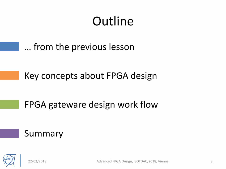
Outline
• … from the previous lesson
• Key concepts about FPGA design
• FPGA gateware design work flow
• Summary
22/02/2018 Advanced FPGA Design, ISOTDAQ 2018, Vienna 3

Outline
• … from the previous lesson
• Key concepts about FPGA design
• FPGA gateware design work flow
• Summary
22/02/2018 Advanced FPGA Design, ISOTDAQ 2018, Vienna 4

What is an FPGA?
A Field-Programmable Gate Array (FPGA) is an integrated circuit designed to be configured by a customer or a designer after manufacturing –hence "field-programmable".
5
… from the previous lesson
https://en.wikipedia.org/wiki/Field-programmable_gate_array
22/02/2018 Advanced FPGA Design, ISOTDAQ 2018, Vienna

FPGA Fabric
• Matrix-like structure
• I/O cells
• Logic cells (LUT, D flip-flops…)
• Configurable interconnect
6
… from the previous lesson
22/02/2018 Advanced FPGA Design, ISOTDAQ 2018, Vienna
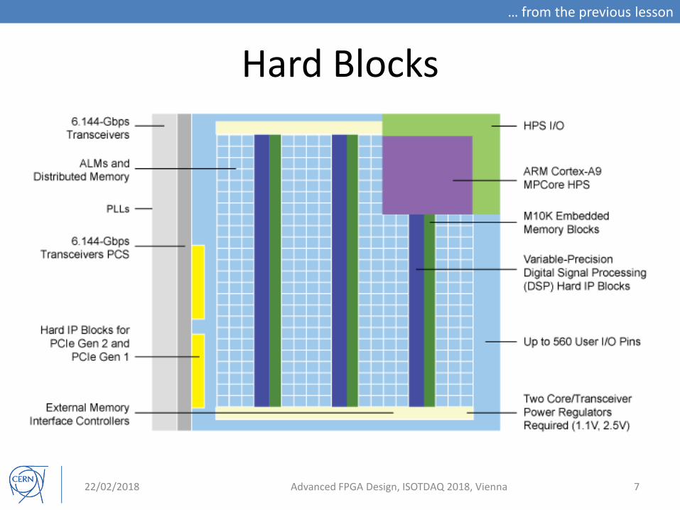
Hard Blocks
7
… from the previous lesson
22/02/2018 Advanced FPGA Design, ISOTDAQ 2018, Vienna

FPGA Design Flow
22/02/2018 Advanced FPGA Design, ISOTDAQ 2018, Vienna 8
… from the previous lesson
101011010101011001010110101010101010110101011010011
1coloring-pages.net

Outline
• … from the previous lesson
• Key concepts about FPGA design
• FPGA gateware design work flow
• Summary
22/02/2018 Advanced FPGA Design, ISOTDAQ 2018, Vienna 9

SequentialProcessing
ParallelProcessing
• Software programming– Code translated into program (set of instructions)
– Program executed sequentially (on CPU)
– Parallelism achieved by running program on multiple cores
– Processing structures and instruction sets are fixed
• FPGA gateware design– Processing structures defined by HW designer
– Individual elements and their connections are described• by schematics or Hardware Description Language (HDL)
– Intrinsically parallel, sequentialbehavior achieved by registers and Finite-State-Machines (FSMs)
FPGA Gateware Designis not a Programming
22/02/2018 Advanced FPGA Design, ISOTDAQ 2018, Vienna 10
Key concepts about FPGA design

A design abstraction which models a synchronous digital circuit in terms of the flow of digital signals (data) between registers and logical operations performed on those signals
http://en.wikipedia.org/wiki/Register-transfer_levelRegister Transfer Level (RTL)
HDL is Used for Describing Hardware
22/02/2018 Advanced FPGA Design, ISOTDAQ 2018, Vienna 11
• Example of a WAIT statement (programming language vs. HDL)
• In programming language (e.g. C, Unix, #include <unistd.h>)
• In HDL (e.g. VHDL):
o Not synthesizable (only for simulation test benches)
o Synthesizable (for simulation and FPGA implementation)
sleep(5); // sleep 5 seconds
Key concepts about FPGA design

HDL is Used for Describing Hardware
22/02/2018 Advanced FPGA Design, ISOTDAQ 2018, Vienna 12
• Example of a WAIT statement (programming language vs. HDL)
• In programming language (e.g. C, Unix, #include <unistd.h>)
• In HDL (e.g. VHDL):
o Not synthesizable (only for simulation test benches)
o Synthesizable (for simulation and FPGA implementation)
sleep(5); // sleep 5 seconds
Key concepts about FPGA design
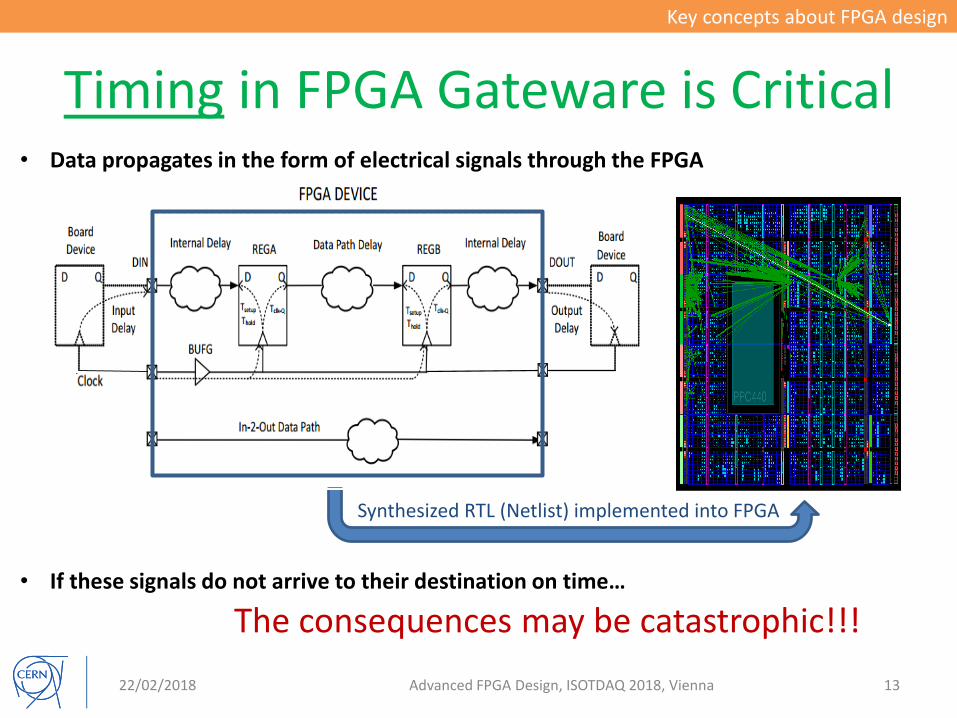
Timing in FPGA Gateware is Critical
22/02/2018 Advanced FPGA Design, ISOTDAQ 2018, Vienna 13
• Data propagates in the form of electrical signals through the FPGA
• If these signals do not arrive to their destination on time…
The consequences may be catastrophic!!!
Synthesized RTL (Netlist) implemented into FPGA x
Key concepts about FPGA design

When designing FPGA gateware you have to think HARDWARE
22/02/2018 Advanced FPGA Design, ISOTDAQ 2018, Vienna 14
…
Key concepts about FPGA design

Outline
• … from the previous lesson
• Key concepts about FPGA design
• FPGA gateware design work flow
• Summary
22/02/2018 Advanced FPGA Design, ISOTDAQ 2018, Vienna 15
22/02/2018 Advanced FPGA Design, ISOTDAQ 2018, Vienna 16
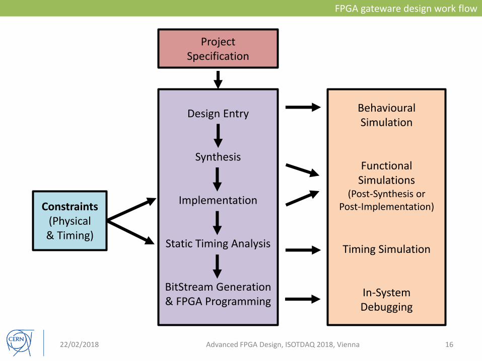
FPGA gateware design work flow
ProjectSpecification
Behavioural Simulation
Functional Simulations
(Post-Synthesis or Post-Implementation)
Timing Simulation
In-SystemDebugging
Constraints(Physical & Timing)
Design Entry
Synthesis
Implementation
Static Timing Analysis
BitStream Generation& FPGA Programming

Project Specification
22/02/2018 Advanced FPGA Design, ISOTDAQ 2018, Vienna 17
This is the most critical step…
The rest of the design process is based on it!
FPGA gateware design work flow

Project Specification
22/02/2018 Advanced FPGA Design, ISOTDAQ 2018, Vienna 18
FPGA gateware design work flow
1. Gather requirements
2. Specify:

Project Specification
22/02/2018 Advanced FPGA Design, ISOTDAQ 2018, Vienna 19
Application Specific Gateware
FPGA gateware design work flow
1. Gather requirements
2. Specify:
– Target application (specific or general purpose)

Project Specification
22/02/2018 Advanced FPGA Design, ISOTDAQ 2018, Vienna 20
General Purpose Gateware
FPGA gateware design work flow
1. Gather requirements
2. Specify:
– Target application (specific or general purpose)

Project Specification
22/02/2018 Advanced FPGA Design, ISOTDAQ 2018, Vienna 21
FPGA gateware design work flow
1. Gather requirements
2. Specify:
– Target application (specific or general purpose)
– Features needed (SoC, multi-gigabit transceivers…)

1. Gather requirements
2. Specify:
– Target application (specific or general purpose)
– Features needed (SoC, multi-gigabit transceivers…)
– FPGA vendor (Xilinx, Intel (Altera), Microsemi (Actel), Lattice…)
Project Specification
22/02/2018 Advanced FPGA Design, ISOTDAQ 2018, Vienna 22
Small FPGA vendors may target specific markets(Microsemi offers high reliable FPGAs…)
FPGA gateware design work flow
FPGA market-share by 2010 (M$)

1. Gather requirements
2. Specify:
– Target application (specific or general purpose)
– Features needed (SoC, multi-gigabit transceivers…)
– FPGA vendor (Xilinx, Intel (Altera), Microsemi (Actel), Lattice…)
– Electronic board (custom or COTS*)
Project Specification
22/02/2018 Advanced FPGA Design, ISOTDAQ 2018, Vienna 23
COTS board (Xilinx Devkit)
Custom Board
(*) Commercial Off-The-Shelf (COTS)
FPGA gateware design work flow

1. Gather requirements
2. Specify:
– Target application (specific or general purpose)
– Features needed (SoC, multi-gigabit transceivers…)
– FPGA vendor (Xilinx, Intel (Altera), Microsemi (Actel), Lattice…)
– Electronic board (custom or COTS)
– Development tools (FPGA vendor or commercial)
Project Specification
22/02/2018 Advanced FPGA Design, ISOTDAQ 2018, Vienna 24
FPGA Vendor Tools
Commercial Tools
FPGA gateware design work flow

Project Specification
22/02/2018 Advanced FPGA Design, ISOTDAQ 2018, Vienna 25
FPGA gateware design work flow
1. Gather requirements
2. Specify:
– Target application (specific or general purpose)
– Features needed (SoC, multi-gigabit transceivers…)
– FPGA vendor (Xilinx, Intel (Altera), Microsemi (Actel), Lattice…)
– Electronic board (custom or COTS)
– Development tools (FPGA vendor or commercial)
– Optimization (speed, area, power or none/default)
– Design entry (schematics or HDL – which?)
Project Specification
22/02/2018 Advanced FPGA Design, ISOTDAQ 2018, Vienna 26
HDL most popular for RTL design but…Schematics may be better in some cases
(SoC bus interconnect…)
FPGA gateware design work flow

1. Gather requirements
2. Specify:
– Target application (specific or general purpose)
– Features needed (SoC, multi-gigabit transceivers…)
– FPGA vendor (Xilinx, Intel (Altera), Microsemi (Actel), Lattice…)
– Electronic board (custom or COTS)
– Development tools (FPGA vendor or commercial)
– Optimization (speed, area, power or none/default)
– Design entry (schematics or HDL – which?)
– Coding convention
Project Specification
22/02/2018 Advanced FPGA Design, ISOTDAQ 2018, Vienna 27
Variable Naming Convention
Your code should be readable
FPGA gateware design work flow
How to write• FSM• Synchronizers• …

1. Gather requirements
2. Specify:
– Target application (specific or general purpose)
– Features needed (SoC, multi-gigabit transceivers…)
– FPGA vendor (Xilinx, Intel (Altera), Microsemi (Actel), Lattice…)
– Electronic board (custom or COTS)
– Development tools (FPGA vendor or commercial)
– Optimization (speed, area, power or none/default)
– Design entry (schematics or HDL – which?)
– Coding convention
– Tool interface (GUI, scripts, both)
Project Specification
22/02/2018 Advanced FPGA Design, ISOTDAQ 2018, Vienna 28
Xilinx ISE Tcl console
FPGA gateware design work flow

1. Gather requirements
2. Specify:
– Target application (specific or general purpose)
– Features needed (SoC, multi-gigabit transceivers…)
– FPGA vendor (Xilinx, Intel (Altera), Microsemi (Actel), Lattice…)
– Electronic board (custom or COTS)
– Development tools (FPGA vendor or commercial)
– Optimization (speed, area, power or none/default)
– Design entry (schematics or HDL – which?)
– Coding convention
– Tool interface (GUI, scripts, both)
– Code/project management (SVN, GIT…)
Project Specification
22/02/2018 Advanced FPGA Design, ISOTDAQ 2018, Vienna 29
FPGA gateware design work flow
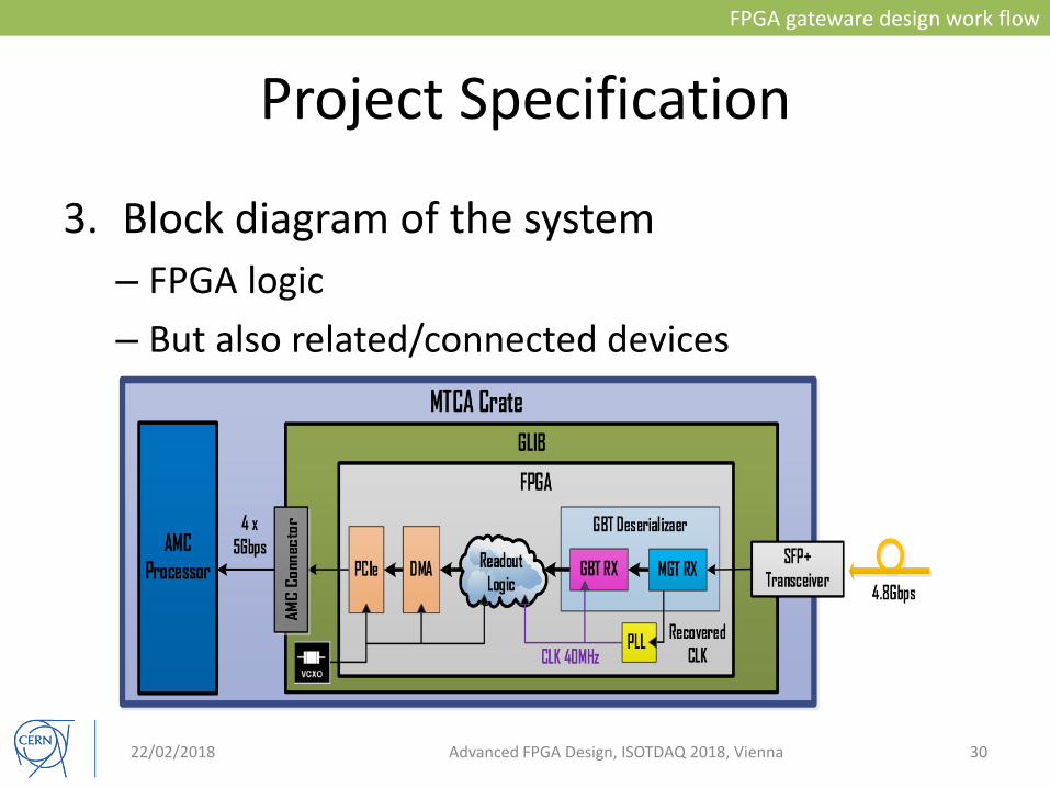
Project Specification
3. Block diagram of the system
– FPGA logic
– But also related/connected devices
22/02/2018 Advanced FPGA Design, ISOTDAQ 2018, Vienna 30
FPGA gateware design work flow

Project Specification
4. Pin planning
– Critical for board development
– One type of location constraints
22/02/2018 Advanced FPGA Design, ISOTDAQ 2018, Vienna 31
FPGA gateware design work flow

• System should be Modular– Modules and instantiations– Separated Data & Control paths– Well defined clock and reset schemes– Design at RTL level (think hard…ware)
• Code should be Reusable– Add primitives (and modules) by inference when possible– Parameterize code (VHDL generics, SystemVerilog parameters…)– Centralize parameters (VHDL packages, SystemVerilog packages…)– Use configurable modules interfaces (VHDL records, SystemVerilog interfaces)– Use standard features (I2C, SPI, Wishbone…)– Use existing IP cores (e.g. from www.OpenCores.org)– Avoid vendor specific IP Cores when possible– Talk with your colleagues and see what other FPGA designers are doing
Design Entry
22/02/2018 Advanced FPGA Design, ISOTDAQ 2018, Vienna 32
PatternGenerator
8-bit Counter
RAM256x16
Increment
Data
Data Valid Flag
Address
Write Enable
Data
Reset
ResetReset
Reset
Clock
16
8
FPGA gateware design work flow

Design Entry: Coding for Synthesis
22/02/2018 Advanced FPGA Design, ISOTDAQ 2018, Vienna 33
FPGA gateware design work flow
HDL
Synthesizablestatements
For synthesis& simulation
Non-synthesizable statements
Only for simulation
VHDL example:

Design Entry: Synchronous Design
• All memory elements are synchronized on clock• Simplifies the designing process• Synchronous design separates:
– Combinatorial logic (logic function)– Sequential logic (memory elements)
• FPGAs architecture and tools are designedto be use with synchronous designs – use it!
22/02/2018 Advanced FPGA Design, ISOTDAQ 2018, Vienna 34
FPGA gateware design work flow
+ =R R
Rst
Combinatorial Logic
Rst

• Combinatorial logic rules
– Sensitivity list must include ALL input signalsOtherwise outputs can be non-responsive under changes of inputs
– ALL output signals must be assigned under ALL possible input conditionsOtherwise undesired latches can be created (asynchronous storage element)
– No feedback from output to input signalsOtherwise unknown output states (metastability) & undesired latches
Design Entry: Synchronous Design
22/02/2018 Advanced FPGA Design, ISOTDAQ 2018, Vienna 35
Asynchronous Latch
FPGA gateware design work flow
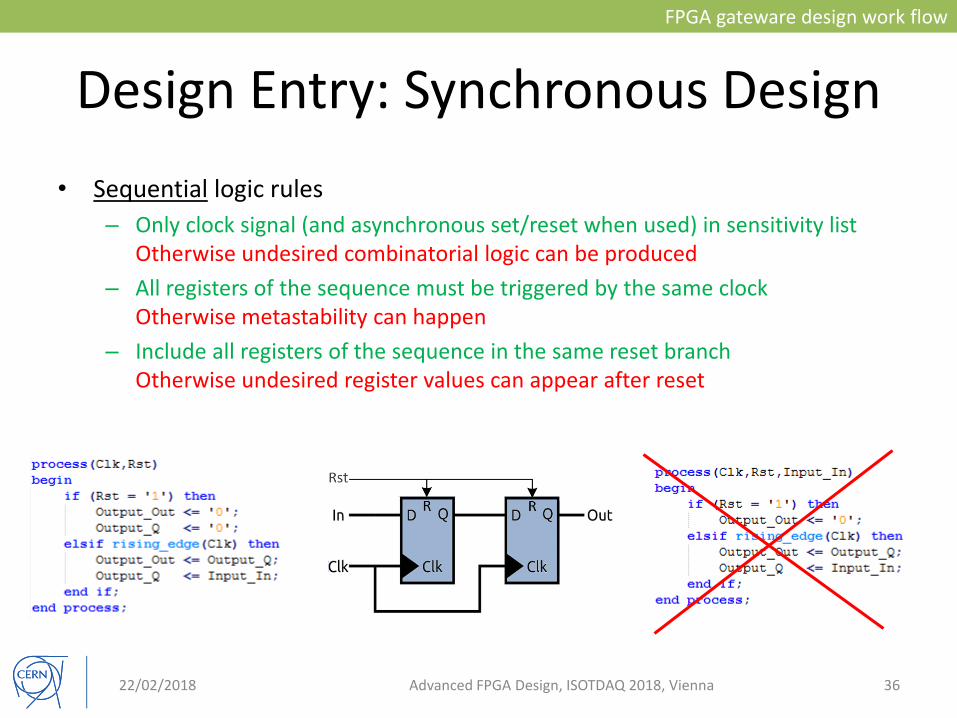
Design Entry: Synchronous Design
22/02/2018 Advanced FPGA Design, ISOTDAQ 2018, Vienna 36
FPGA gateware design work flow
• Sequential logic rules
– Only clock signal (and asynchronous set/reset when used) in sensitivity listOtherwise undesired combinatorial logic can be produced
– All registers of the sequence must be triggered by the same clockOtherwise metastability can happen
– Include all registers of the sequence in the same reset branchOtherwise undesired register values can appear after reset

Design Entry: Synchronous Design
• Synchronous design rules– FULLY synchronous design
• No combinatorial feedback• No asynchronous latches
Otherwise design tools can do incorrect analysis– Time-constrain ALL input/output signals (registering may help)
Otherwise uncontrolled length of paths can happen– Properly design the reset scheme (mentioned later)
Otherwise undesired register values can appear after reset– Properly design the clocking scheme (mentioned later)
Otherwise metastability & resources misuse can happen– Properly handle Clock Domain Crossings (CDC) (mentioned later)
Otherwise metastability can happen
22/02/2018 Advanced FPGA Design, ISOTDAQ 2018, Vienna 37
FPGA gateware design work flow

Design Entry: Finite State Machines
22/02/2018 Advanced FPGA Design, ISOTDAQ 2018, Vienna 38
• Finite State Machines (FSMs):
• Two variants of FSM
o Moore: outputs depends only on the current state of the FSM
• Digital logic circuit with a finite number of internal states
• Used modelling sequential behavior
o Mealy: outputs depends on the current state of the FSM and current values of inputs
• Modelled by State Transition Diagrams
• Many different FSM coding styles (But not all of them are good!!)
• FSM coding considerations:
o Be careful with unreachable/illegal stateso Outputs may be assigned during states or state transitions
FPGA gateware design work flow

Design Entry: Reset Scheme
22/02/2018 Advanced FPGA Design, ISOTDAQ 2018, Vienna 39
• It has a direct impact on:
• Performance
• Logic utilization
• Reliability
• Used to initialize registers outputs to a know state
You should use
SYNCHRONOUS RESET
by default
A bad reset scheme may get you crazy!!!
o No Reset Scheme
Pros; Easier Routing, Less resources, Easiest timing closure
Cons: Only reset at power up (in some devices not even that…)
• Different approaches:
<- In fact, reset is not always needed
o Asynchronous
o Synchronous
o Hybrid: Usually in big designs (Avoid when possible!!!)
Pros: No free running clock required, easier timing closure
Cons: skew, glitches, simulation mismatch, difficult to debug, extra constraints, etc.
Pros: No Skew, No Glitches, No simulation mismatch, Easier to debug, No extra constraints, etc..
Cons: Free-running clock required, More difficult timing closure
FPGA gateware design work flow

Design Entry: Clock Scheme
22/02/2018 Advanced FPGA Design, ISOTDAQ 2018, Vienna 40
• Other FPGA clocking resources
• Bad practices when designing your clocking scheme
Gated clocks Derived clocks
• Clock regions
Clocking resources are very precious!!!
• Clock capable pins
• Clock buffers
• PLLs & DCM
• Clock Multiplexors
Global clock tree
Local clock tree
Clock Regions
FF
FF
Comb
CLK
• Clock trees (Global & Local)
FPGA gateware design work flow

Design Entry: Timing
22/02/2018 Advanced FPGA Design, ISOTDAQ 2018, Vienna 41
Tsu: Set Up TimeTh: Hold Time
Clk
Tsu Th
SamplingPoint
In DATA[0] DATA[1]
DATA[0] DATA[1]Out
FPGA gateware design work flow
Input data has to be stable here!Otherwise metastability can happen.

Design Entry: Timing
22/02/2018 Advanced FPGA Design, ISOTDAQ 2018, Vienna 42
• Clock Domain Crossing (CDC): The problem
Signal violates the setup-time of FlipFlop B clocked by Clk B
Bout becomes metastable and then settles at either at ‘1’ or ‘0’
• Clock Domain Crossing (CDC) : passing a signal from one clock domain to another (A to B)
• If clocks are unrelated to each other (asynchronous) timing analysis is not possible
• Setup and Hold times of FlipFlop B are likely to be violated -> Metastability!!!
FPGA gateware design work flow

Design Entry: Timing
22/02/2018 Advanced FPGA Design, ISOTDAQ 2018, Vienna 43
• Clock Domain Crossing (CDC)
FPGA gateware design work flow

Design Entry: Timing
22/02/2018 Advanced FPGA Design, ISOTDAQ 2018, Vienna 44
• Clock Domain Crossing (CDC): The solution
Handshaking DPRAMSynchronizers
Be aware of FIFO overflow/underflow!!!
Clock phase alignment
Din
Wr Addr Rd Addr
Wr Clk Rd Clk
Wr En Rr En
Dout
‘1’ ‘1’
[0...0][0...0]
Asynchronous
FIFO
Din
Wr Clk Rd Clk
Wr En Rr En
Dout
Full Empty
FPGA gateware design work flow
Avoid creating unnecessary clock domains

Design Entry: Primitives & IP Cores
22/02/2018 Advanced FPGA Design, ISOTDAQ 2018, Vienna 45
• Hard IP Cores: Complex hardware blocks embedded into the FPGA
• Soft IP Cores: Complex (or simple) modules ready to be implemented
• Vendor (and device) specific
• Fixed I/O location
• In many cases they may be set through GUI (wizards)
• E.g. PLLs, multi-gigabit transceivers, Ethernet MAC, CPU…
• They may be
• vendor specific (encryption code, memory controller…) or
• vendor agnostic (commercial or open source (www.OpenCores.org))
• In many cases they may be set through GUI (wizards)
• Primitives: Basic components of the FPGA
• Vendor (and device) specific
• E.g. buffers (I/O & clock), registers, BRAMs, DSP blocks…
• Two ways of adding Primitives & IP Cores to your system:
Instantiated FlipFlop
(for Microsemi ProAsic3)
Inferred FlipFlop (Verilog)
• Instantiation: The module is EXPLICITLY added to the system
• Inference: The module is IMPLICITLY added to the system
FPGA gateware design work flow

Synthesis
22/02/2018 Advanced FPGA Design, ISOTDAQ 2018, Vienna 46
• The FPGA design tool optimizes the design during synthesis
• What does it do?
• Defines the connection of these elementary functions
• Translates the schematic or HDL code into elementary logic functions
It may do undesired changes to the system (e.g. remove modules, change signal names, etc.)!!!
• Always check the synthesis report
• And also check the RTL/Technology viewers
• Warnings & Errors
• Optimizations
• Estimated resource utilization
• And more…
Example of RTL Schematic
Example of Synthesis Report
FPGA gateware design work flow

• Timing requirements for all paths must be provided to the FPGA design tool
• To efficiently specify these constraints:
• Most common types of constraints
• Input paths
• Output paths
• Register-to-register paths (combinatorial paths)
• Path specific exceptions (e.g. false path, multi-cycle paths, etc.)
1) Begin with global constraints
2) Add path specific exceptions as needed (only for special cases)
• Over-constrained system is difficult to route
Constraints: Timing
22/02/2018 Advanced FPGA Design, ISOTDAQ 2018, Vienna 47
Timing constraint (Xilinx .ucf)
• Defined in a constraint files (Xilinx .XDC, Altera .SDC) – can be generated in GUI
FPGA gateware design work flow

Constraints: Physical
22/02/2018 Advanced FPGA Design, ISOTDAQ 2018, Vienna 48
• Pin planning
• Floorplanning
As previously mentioned…
You should prepare Pin Planning
during Specification Stage
• Only when really needed
• To place logic close to their related I/O pins
• To avoid routing across the chip
• Can improve timing (faster system speed)
• Over-constrained system is difficult to route
FPGA gateware design work flow

• The FPGA design tool:
1) Translates timing and physical constraints in order to guide the implementation
Implementation
22/02/2018 Advanced FPGA Design, ISOTDAQ 2018, Vienna 49
• The FPGA design tool may be set for different optimizations (Speed, Area, Power or none)
• Physical placement and timing change after re-implementing (use constraints to minimize these changes)
2) Maps the synthesized netlist:
3) Places and Routes (P&R) the mapped netlist:
o Logic elements to FPGA logic cells
o Hard IP cores to FPGA hard blocks
o Verifies that the design can fit the target device
o Physical placement of the FPGA logic cells
o Routing of the signals through the interconnect network & clock tree
o Physical placement of the FPGA hard blocks
• You should always check the different reports generated during implementation
FPGA gateware design work flow

Static Timing Analysis
22/02/2018 Advanced FPGA Design, ISOTDAQ 2018, Vienna 50
• The FPGA design tool analyses the signals propagation delays and clock relationships after implementation
• A timing report is generated, including the paths that did not meet the timing requirements
• The timing closure flow:
• Setup violations: Too long combinatorial paths
• Rule of thumb for timing violations:
• Hold violations: Issue with CDC and/or path specific exceptions
FPGA gateware design work flow

Bitstream Generation& FPGA Programming
22/02/2018 Advanced FPGA Design, ISOTDAQ 2018, Vienna 51
• Binary file containing the FPGA configuration data
• Bitstream is loaded into the FPGA through JTAG or SPI
• Configuration data may be stored in on-board FLASH and loaded by the FPGA at power up
• Bitstream:
• FPGA programming:
• Each FPGA vendor has its own bitstream file format (e.g. .bit (Xilinx), .sof (Altera) )
User image
(bitstream 2)
CORRUPTED
or
INCORRECT
Power up
Golden image
(bitstream 1)
Fallback (CORRUPTED)
Power cycle (INCORRECT)
Auto
Manual Trigger (ICAP)Multiboot/Safe FPGA configuration diagrams
• Multiboot/Safe FPGA configuration
• Remote programming (e.g. through Ethernet)
FPGA gateware design work flow

Simulation
22/02/2018 Advanced FPGA Design, ISOTDAQ 2018, Vienna 52
• HDL simulators:
• Most popular: Modelsim
• Other simulators: Vivado Simulator (Xilinx), Icarus Verilog (Open-source)…
• Different levels of simulation
• Event-based simulation to recreate the parallel nature of digital designs
• Verification of individual modules or full systems
• Behavioral: simulates only the behavior of the design
• Functional: uses realistic functional models for the target technology
• Timing: most accurate, uses Implemented design
Slow
Fast
Very Slow
Simulator wave window
FPGA gateware design work flow

In-System Analyzers & Virtual I/Os
22/02/2018 Advanced FPGA Design, ISOTDAQ 2018, Vienna 53
• Your design is up… and also running?
• Can be embedded into the design and controlled by JTAG
• Most FPGA vendors provide in-system analyzers & virtual I/Os
• Allow monitoring but also controlling the FPGA signals
• Minimize interfering with your system by:
• It is useful to spy inside the FPGA… but the issue may come from the rest of the board!!!
• Remember… it is HARDWARE
Placing extra registers between the monitored signals and the In-System Analyser
In-System Analyser (Altera SignalTap II)
Virtual I/Os (Xilinx VIO)
FPGA gateware design work flow

Pattern
Generator
8-bit Counter
RAM256x16-bit
Increment
Data
Data Valid Flag
Address
Write Enable
Data
Reset
ResetReset
Reset
Clock
16-bit
8-bit
Debugging Techniques
22/02/2018 Advanced FPGA Design, ISOTDAQ 2018, Vienna 54
Divide & Conquer Follow the chain
“Open the box”
We are debugging HARDWARE
FPGA gateware design work flow

After debugging…
22/02/2018 Advanced FPGA Design, ISOTDAQ 2018, Vienna 55
• Maintenance
• … and maybe User Support
• Documentation
FPGA gateware design work flow

Outline
• … from the previous lesson
• Key concepts about FPGA design
• FPGA gateware design work flow
• Summary
22/02/2018 Advanced FPGA Design, ISOTDAQ 2018, Vienna 56

What to Remember
• FPGA gateware design is not a programming
• HDL are used for describing hardware
• Timing is critical in FPGA gateware design
22/02/2018 Advanced FPGA Design, ISOTDAQ 2018, Vienna 57
Summary

What to Remember – GW Flow
• Plan, plan and plan again
• Modular and reusable system
• Coding for synthesis
• Resets and clocks schemes
• Clock Domain Crossing
• Constraint the design properly
• Read all the reports
• Be methodic when debugging & use all tools available
• A running system is not the end of the road… (documentation, maintenance, user support)
22/02/2018 Advanced FPGA Design, ISOTDAQ 2018, Vienna 58
Summary

Additional Resources
• There are nice papers & books but…
• FPGA vendors provide very good documentation about all topics mentioned in this lecture
22/02/2018 Advanced FPGA Design, ISOTDAQ 2018, Vienna 59
Summary
