adding ip to a hardware design using axi - dc.uba.ar · push buttons and dip switches on the nexys3...
TRANSCRIPT

Lab Workbook Adding IP to a Hardware Design Using AXI
www.xilinx.com/university Nexys3 2-1 [email protected] © Copyright 2012 Xilinx
Adding IP to a Hardware Design Using AXI
Introduction
This lab guides you through the process of adding additional IP to an existing processor system by using Xilinx Platform Studio (XPS). You will add GPIO peripherals from the IP Catalog tab to interface to the push buttons and DIP switches on the Nexys3 Board. At the end of the lab, you will generate the bitstream and test the peripherals in hardware.
Objectives
After completing this lab, you will be able to:
• Add additional IP to a hardware design • Update ucf file to support external ports of the added IP
• Setup some of the compiler settings
Procedure
This lab is separated into steps that consist of general overview statements that provide information on the detailed instructions that follow. Follow these detailed instructions to progress through the lab.
This lab comprises 6 primary steps: You will open the project, add and configure GPIO peripherals in the system, make ports external, analyze the MHS file, create TestApp application in SDK, and, finally, verify the design in hardware.
Design Description
The purpose of this lab exercise is to extend the hardware design (Figure 1) created in Lab 1
Figure 1. Extend the System from the previous

Adding IP to a Hardware Design Using AXI Lab Workbook
Nexys3 2-2 www.xilinx.com/university [email protected] © Copyright 2012 Xilinx
General Flow for this Lab
Open the Project Step 1
1-1. Create a lab2 folder and copy the contents of the lab1 folder into the lab2
folder, or copy the content of the labsolution\lab1 folder into the lab2 folder. Launch Xilinx Platform Studio (XPS) and open the project file.
1-1-1. Create a lab2 folder in the c:\xup\embedded\labs directory and copy the contents from lab1 to lab2 or copy the content of the labsolution/lab1 folder to lab2
1-1-2. Open XPS by selecting Start > All Programs > Xilinx Design Tools > ISE Design Suite 14.2 > EDK > Xilinx Platform Studio.
1-1-3. Select Open project, and browse to C:\xup\embedded\labs\lab2.
1-1-4. Click system.xmp, and click Open to open the project.
Add and Connect GPIO Peripherals to the System Step 2
2-1. Add two instances of an XPS GPIO Peripheral from the IP catalog to the processor system via the System Assembly View.
XPS provides two methods for adding peripherals to an existing project. You will use the first method, the System Assembly View panel, to add most of the additional IP and connect them. The second method is to manually edit MHS file.
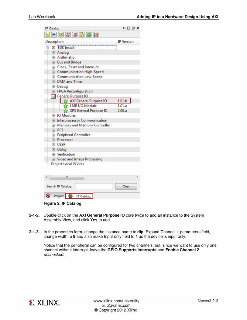
2-1-1. Select the IP Catalog tab in the left window and click on plus sign next to General Purpose IO entry to view the available cores under it.
Step 1: Open the project
Step 2: Add and connect GPIO
peripherals in the system
Step 3: Make
external GPIO
connections
Step 4: Analyze the
MHS file
Step 5: Create
TestApp application in
SDK
Step 6: Verify the design in hardware
Lab Workbook Adding IP to a Hardware Design Using AXI
www.xilinx.com/university Nexys3 2-3 [email protected] © Copyright 2012 Xilinx
Figure 2. IP Catalog
2-1-2. Double-click on the AXI General Purpose IO core twice to add an instance to the System Assembly View, and click Yes to add.
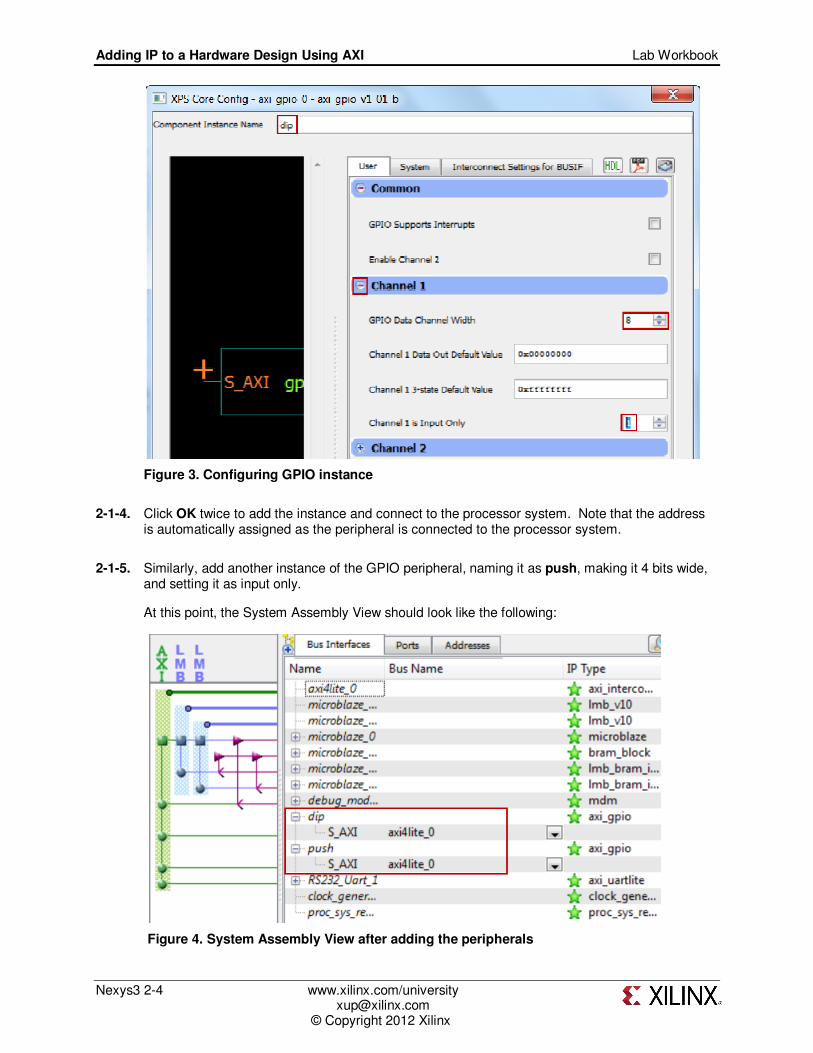
2-1-3. In the properties form, change the instance name to dip. Expand Channel 1 parameters field, change width to 8 and also make Input only field to 1 as the device is input only.
Notice that the peripheral can be configured for two channels, but, since we want to use only one channel without interrupt, leave the GPIO Supports Interrupts and Enable Channel 2 unchecked.
Adding IP to a Hardware Design Using AXI Lab Workbook
Nexys3 2-4 www.xilinx.com/university [email protected] © Copyright 2012 Xilinx
Figure 3. Configuring GPIO instance
2-1-4. Click OK twice to add the instance and connect to the processor system. Note that the address is automatically assigned as the peripheral is connected to the processor system.
2-1-5. Similarly, add another instance of the GPIO peripheral, naming it as push, making it 4 bits wide, and setting it as input only.
At this point, the System Assembly View should look like the following:
Figure 4. System Assembly View after adding the peripherals
Lab Workbook Adding IP to a Hardware Design Using AXI
www.xilinx.com/university Nexys3 2-5 [email protected] © Copyright 2012 Xilinx
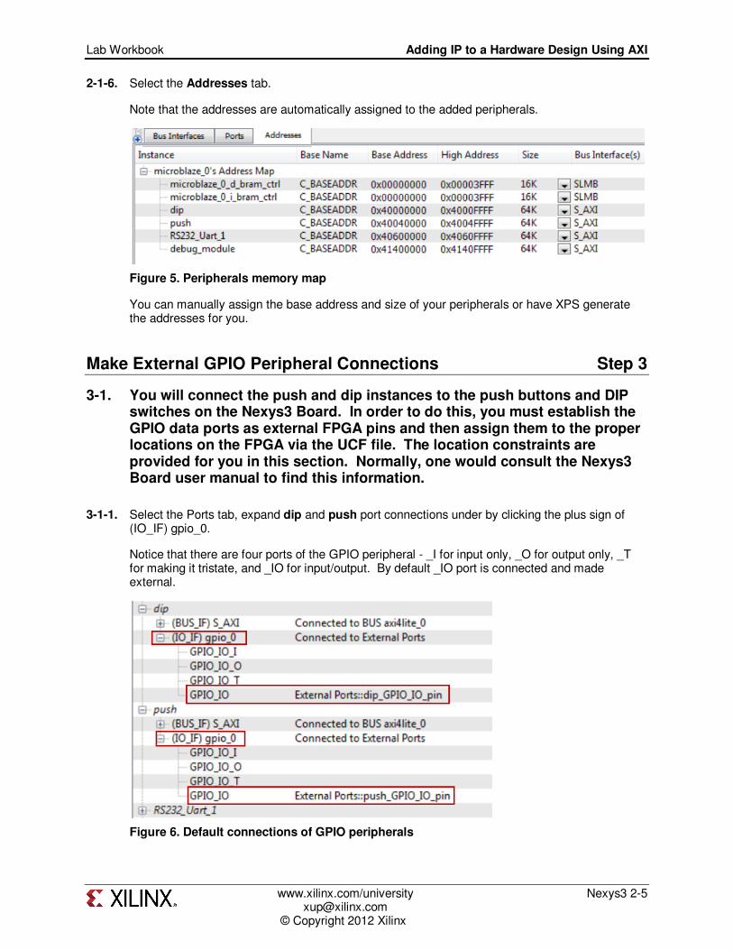
2-1-6. Select the Addresses tab.
Note that the addresses are automatically assigned to the added peripherals.
Figure 5. Peripherals memory map
You can manually assign the base address and size of your peripherals or have XPS generate the addresses for you.
Make External GPIO Peripheral Connections Step 3
3-1. You will connect the push and dip instances to the push buttons and DIP switches on the Nexys3 Board. In order to do this, you must establish the GPIO data ports as external FPGA pins and then assign them to the proper locations on the FPGA via the UCF file. The location constraints are provided for you in this section. Normally, one would consult the Nexys3 Board user manual to find this information.
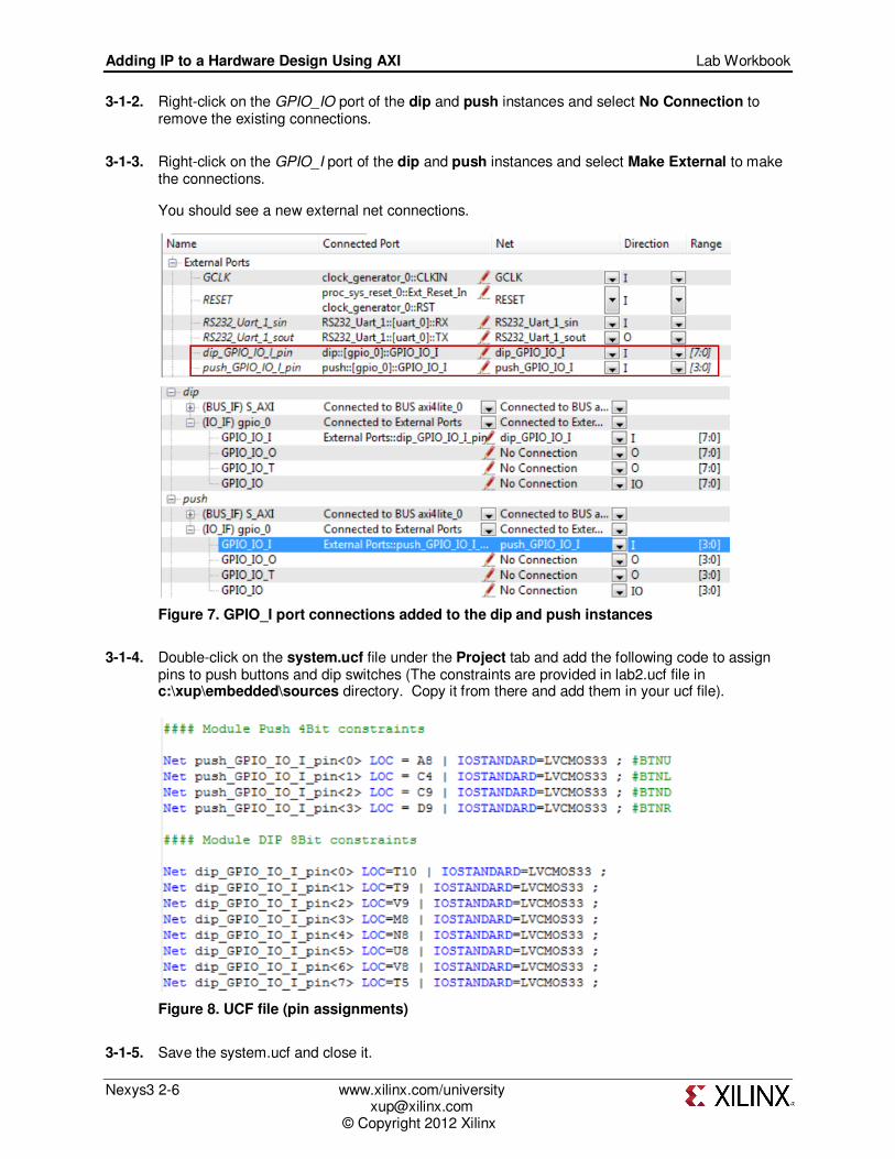
3-1-1. Select the Ports tab, expand dip and push port connections under by clicking the plus sign of (IO_IF) gpio_0.
Notice that there are four ports of the GPIO peripheral - _I for input only, _O for output only, _T for making it tristate, and _IO for input/output. By default _IO port is connected and made external.
Figure 6. Default connections of GPIO peripherals
Adding IP to a Hardware Design Using AXI Lab Workbook
Nexys3 2-6 www.xilinx.com/university [email protected] © Copyright 2012 Xilinx
3-1-2. Right-click on the GPIO_IO port of the dip and push instances and select No Connection to remove the existing connections.
3-1-3. Right-click on the GPIO_I port of the dip and push instances and select Make External to make the connections.
You should see a new external net connections.
Figure 7. GPIO_I port connections added to the dip and push instances
3-1-4. Double-click on the system.ucf file under the Project tab and add the following code to assign pins to push buttons and dip switches (The constraints are provided in lab2.ucf file in c:\xup\embedded\sources directory. Copy it from there and add them in your ucf file).
Figure 8. UCF file (pin assignments)
3-1-5. Save the system.ucf and close it.
Lab Workbook Adding IP to a Hardware Design Using AXI
www.xilinx.com/university Nexys3 2-7 [email protected] © Copyright 2012 Xilinx
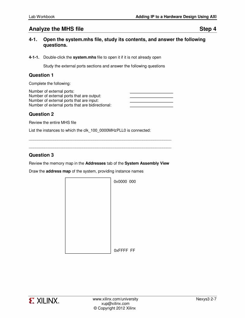
Analyze the MHS file Step 4
4-1. Open the system.mhs file, study its contents, and answer the following questions.
4-1-1. Double-click the system.mhs file to open it if it is not already open
Study the external ports sections and answer the following questions
Question 1
Complete the following:
Number of external ports: Number of external ports that are output: Number of external ports that are input: Number of external ports that are bidirectional:
Question 2
Review the entire MHS file
List the instances to which the clk_100_0000MHzPLL0 is connected:
________________________________________________________________
________________________________________________________________
Question 3
Review the memory map in the Addresses tab of the System Assembly View
Draw the address map of the system, providing instance names
0x0000_000
0xFFFF_FF

Adding IP to a Hardware Design Using AXI Lab Workbook
Nexys3 2-8 www.xilinx.com/university [email protected] © Copyright 2012 Xilinx
Generate TestApp Application in SDK Step 5
5-1. Start SDK from XPS, generate software platform project with default settings.
5-1-1. Start SDK by clicking Project > Export Hardware Design to SDK or click on left Navigator.
5-1-2. Click on Export & Launch SDK button with default settings.
Since we have not generated hardware bitstream and the default option is selected, a hardware bitstream will be generated and then SDK will be open
5-1-3. In Select a workspace window, locate c:\xup\embedded\labs\lab2\SDK\SDK_Export and click OK.
5-1-4. In SDK, select File > New > Xilinx Board Support Package.
5-1-5. Click Finish with default settings (with standalone operating system).
This will open the Software Platform Settings form showing the OS and libraries selections.
Figure 9. Board Support Package settings
5-1-6. Click OK to accept the default settings, as we want to create a standalone_bsp_0 software platform project without requiring any additional libraries support.

Lab Workbook Adding IP to a Hardware Design Using AXI
www.xilinx.com/university Nexys3 2-9 [email protected] © Copyright 2012 Xilinx
5-1-7. The library generator will run in the background and will create xparameters.h file in the C:\xup\embedded\labs\lab2\SDK\SDK_Export\standalone_bsp_0\microblaze_0\include\ directory.
5-2. Create an empty application project and import the provided lab2.c file.
5-2-1. Select Standalone_bsp_0 in the project view, right-click, and select New > Project.
5-2-2. Select Xilinx C Project and then click Next.
5-2-3. Select Empty Application in the Select Project Template window, and enter TestApp as the Project Name and click Next.

Adding IP to a Hardware Design Using AXI Lab Workbook
Nexys3 2-10 www.xilinx.com/university [email protected] © Copyright 2012 Xilinx
Figure 10. Create a blank C Project
5-2-4. Select Target an existing Board Support Package option, then select standalone_bsp_0, and click Finish.

Lab Workbook Adding IP to a Hardware Design Using AXI
www.xilinx.com/university Nexys3 2-11 [email protected] © Copyright 2012 Xilinx
Figure 11. Use Existing Board Support Package
The TestApp project will be created in the Project Explorer window of SDK.
5-2-5. Select TestApp in the project view, right-click, and select Import.
5-2-6. Expand General category and double-click on File System.
5-2-7. Browse to c:\xup\embedded\sources folder.
5-2-8. Select lab2.c and click Finish.
A snippet of the source code is shown in figure below.

Adding IP to a Hardware Design Using AXI Lab Workbook
Nexys3 2-12 www.xilinx.com/university [email protected] © Copyright 2012 Xilinx
Figure 12. Snippet of source code
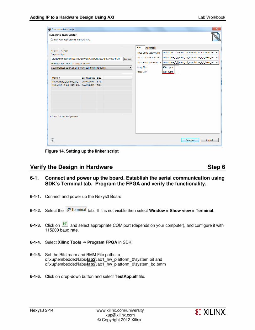
5-3. Set build setting to no optimization and generate linker script which targets the application to the ilmb and dlmb memories as well as have 400 bytes of heap and stack each
5-3-1. Select TestApp project, right-click, and select C/C++ Build Settings
5-3-2. Select Optimization option of the MicroBlaze gcc compiler in the Tool Settings tab and make sure that the Optimization Level is set to None (-O0) as we have a software loop acting as a delay loop and we do not want it to be optimized away.

Lab Workbook Adding IP to a Hardware Design Using AXI
www.xilinx.com/university Nexys3 2-13 [email protected] © Copyright 2012 Xilinx
Figure 13. Setting the compiler settings
5-3-3. Select TestApp, right-click and select Generate Linker Script.
5-3-4. Target everything to ilmb and dlmb memories, and set heap and stack to 400 bytes each.
5-3-5. Click on the Generate button, and click Yes to overwrite the existing linker script file.
Adding IP to a Hardware Design Using AXI Lab Workbook
Nexys3 2-14 www.xilinx.com/university [email protected] © Copyright 2012 Xilinx
Figure 14. Setting up the linker script
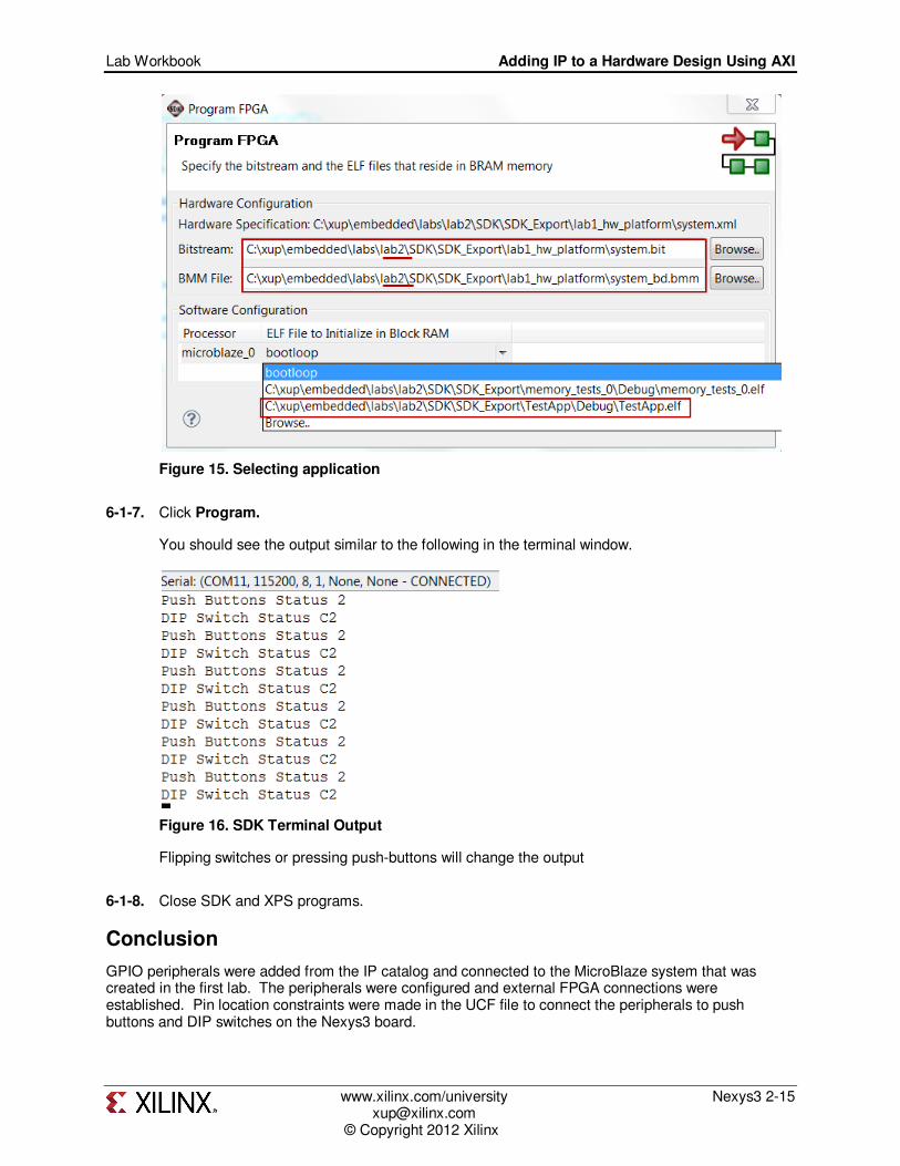
Verify the Design in Hardware Step 6
6-1. Connect and power up the board. Establish the serial communication using SDK’s Terminal tab. Program the FPGA and verify the functionality.
6-1-1. Connect and power up the Nexys3 Board.
6-1-2. Select the tab. If it is not visible then select Window > Show view > Terminal.
6-1-3. Click on and select appropriate COM port (depends on your computer), and configure it with 115200 baud rate.
6-1-4. Select Xilinx Tools ���� Program FPGA in SDK.
6-1-5. Set the Bitstream and BMM File paths to c:\xup\embedded\labs\lab2\lab1_hw_platform_0\system.bit and c:\xup\embedded\labs\lab2\lab1_hw_platform_0\system_bd.bmm
6-1-6. Click on drop-down button and select TestApp.elf file.
Lab Workbook Adding IP to a Hardware Design Using AXI
www.xilinx.com/university Nexys3 2-15 [email protected] © Copyright 2012 Xilinx
Figure 15. Selecting application
6-1-7. Click Program.
You should see the output similar to the following in the terminal window.
Figure 16. SDK Terminal Output
Flipping switches or pressing push-buttons will change the output
6-1-8. Close SDK and XPS programs.
Conclusion
GPIO peripherals were added from the IP catalog and connected to the MicroBlaze system that was created in the first lab. The peripherals were configured and external FPGA connections were established. Pin location constraints were made in the UCF file to connect the peripherals to push buttons and DIP switches on the Nexys3 board.

Adding IP to a Hardware Design Using AXI Lab Workbook
Nexys3 2-16 www.xilinx.com/university [email protected] © Copyright 2012 Xilinx
Answers
1. Complete the following:
Number of external ports: 6 Number of external ports that are output: 1 Number of external ports that are input: 5 Number of external ports that are bidirectional: 0
2. List the instances to which the clk_100_0000MHzPLL0 is connected:
axi4lite_0, proc_sys_reset_0, microblaze_0, microblaze_0_ilmb, microblaze_0_dlmb, microblaze_0_i_bram_ctrl, microblaze_0_d_bram_ctrl, RS232_Uart_1, debug_module, dip, push, clock_generator_0
3. Draw the address map of the system, providing instance names. You can sort the peripheral addresses by base address from the Addresses tab.
0x00000000–0x00003fff dlmb, llmb
unused
0x40000000– 0x4000ffff dip
0x40040000– 0x4004ffff push
0x40600000– 0x4060ffff RS232_Uart_1
0x41400000– 0x4140ffff debug_module

Lab Workbook Adding IP to a Hardware Design Using AXI
www.xilinx.com/university Nexys3 2-17 [email protected] © Copyright 2012 Xilinx
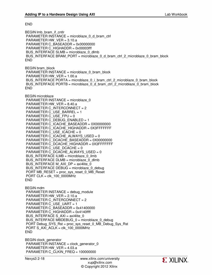
Completed MHS File # ############################################################################## # Created by Base System Builder Wizard for Xilinx EDK 14.2 Build EDK_P.28xd # Wed Sep 19 09:57:18 2012 # Target Board: digilent nexys3 Rev B # Family: spartan6 # Device: xc6slx16 # Package: csg324 # Speed Grade: -3 # ############################################################################## PARAMETER VERSION = 2.1.0 PORT RS232_Uart_1_sout = RS232_Uart_1_sout, DIR = O PORT RS232_Uart_1_sin = RS232_Uart_1_sin, DIR = I PORT RESET = RESET, DIR = I, SIGIS = RST, RST_POLARITY = 1 PORT GCLK = GCLK, DIR = I, SIGIS = CLK, CLK_FREQ = 100000000 PORT dip_GPIO_IO_I_pin = dip_GPIO_IO_I, DIR = I, VEC = [7:0] PORT push_GPIO_IO_I_pin = push_GPIO_IO_I, DIR = I, VEC = [3:0] BEGIN proc_sys_reset PARAMETER INSTANCE = proc_sys_reset_0 PARAMETER HW_VER = 3.00.a PARAMETER C_EXT_RESET_HIGH = 1 PORT MB_Debug_Sys_Rst = proc_sys_reset_0_MB_Debug_Sys_Rst PORT Dcm_locked = proc_sys_reset_0_Dcm_locked PORT MB_Reset = proc_sys_reset_0_MB_Reset PORT Slowest_sync_clk = clk_100_0000MHz PORT Interconnect_aresetn = proc_sys_reset_0_Interconnect_aresetn PORT Ext_Reset_In = RESET PORT BUS_STRUCT_RESET = proc_sys_reset_0_BUS_STRUCT_RESET END BEGIN lmb_v10 PARAMETER INSTANCE = microblaze_0_ilmb PARAMETER HW_VER = 2.00.b PORT SYS_RST = proc_sys_reset_0_BUS_STRUCT_RESET PORT LMB_CLK = clk_100_0000MHz END BEGIN lmb_bram_if_cntlr PARAMETER INSTANCE = microblaze_0_i_bram_ctrl PARAMETER HW_VER = 3.10.a PARAMETER C_BASEADDR = 0x00000000 PARAMETER C_HIGHADDR = 0x00003fff BUS_INTERFACE SLMB = microblaze_0_ilmb BUS_INTERFACE BRAM_PORT = microblaze_0_i_bram_ctrl_2_microblaze_0_bram_block END BEGIN lmb_v10 PARAMETER INSTANCE = microblaze_0_dlmb PARAMETER HW_VER = 2.00.b PORT SYS_RST = proc_sys_reset_0_BUS_STRUCT_RESET PORT LMB_CLK = clk_100_0000MHz
Adding IP to a Hardware Design Using AXI Lab Workbook
Nexys3 2-18 www.xilinx.com/university [email protected] © Copyright 2012 Xilinx
END BEGIN lmb_bram_if_cntlr PARAMETER INSTANCE = microblaze_0_d_bram_ctrl PARAMETER HW_VER = 3.10.a PARAMETER C_BASEADDR = 0x00000000 PARAMETER C_HIGHADDR = 0x00003fff BUS_INTERFACE SLMB = microblaze_0_dlmb BUS_INTERFACE BRAM_PORT = microblaze_0_d_bram_ctrl_2_microblaze_0_bram_block END BEGIN bram_block PARAMETER INSTANCE = microblaze_0_bram_block PARAMETER HW_VER = 1.00.a BUS_INTERFACE PORTA = microblaze_0_i_bram_ctrl_2_microblaze_0_bram_block BUS_INTERFACE PORTB = microblaze_0_d_bram_ctrl_2_microblaze_0_bram_block END BEGIN microblaze PARAMETER INSTANCE = microblaze_0 PARAMETER HW_VER = 8.40.a PARAMETER C_INTERCONNECT = 2 PARAMETER C_USE_BARREL = 1 PARAMETER C_USE_FPU = 0 PARAMETER C_DEBUG_ENABLED = 1 PARAMETER C_ICACHE_BASEADDR = 0X00000000 PARAMETER C_ICACHE_HIGHADDR = 0X3FFFFFFF PARAMETER C_USE_ICACHE = 0 PARAMETER C_ICACHE_ALWAYS_USED = 0 PARAMETER C_DCACHE_BASEADDR = 0X00000000 PARAMETER C_DCACHE_HIGHADDR = 0X3FFFFFFF PARAMETER C_USE_DCACHE = 0 PARAMETER C_DCACHE_ALWAYS_USED = 0 BUS_INTERFACE ILMB = microblaze_0_ilmb BUS_INTERFACE DLMB = microblaze_0_dlmb BUS_INTERFACE M_AXI_DP = axi4lite_0 BUS_INTERFACE DEBUG = microblaze_0_debug PORT MB_RESET = proc_sys_reset_0_MB_Reset PORT CLK = clk_100_0000MHz END BEGIN mdm PARAMETER INSTANCE = debug_module PARAMETER HW_VER = 2.10.a PARAMETER C_INTERCONNECT = 2 PARAMETER C_USE_UART = 1 PARAMETER C_BASEADDR = 0x41400000 PARAMETER C_HIGHADDR = 0x4140ffff BUS_INTERFACE S_AXI = axi4lite_0 BUS_INTERFACE MBDEBUG_0 = microblaze_0_debug PORT Debug_SYS_Rst = proc_sys_reset_0_MB_Debug_Sys_Rst PORT S_AXI_ACLK = clk_100_0000MHz END BEGIN clock_generator PARAMETER INSTANCE = clock_generator_0 PARAMETER HW_VER = 4.03.a PARAMETER C_CLKIN_FREQ = 100000000

Lab Workbook Adding IP to a Hardware Design Using AXI
www.xilinx.com/university Nexys3 2-19 [email protected] © Copyright 2012 Xilinx
PARAMETER C_CLKOUT0_FREQ = 100000000 PARAMETER C_CLKOUT0_GROUP = NONE PORT LOCKED = proc_sys_reset_0_Dcm_locked PORT CLKOUT0 = clk_100_0000MHz PORT RST = RESET PORT CLKIN = GCLK END BEGIN axi_interconnect PARAMETER INSTANCE = axi4lite_0 PARAMETER HW_VER = 1.06.a PARAMETER C_INTERCONNECT_CONNECTIVITY_MODE = 0 PORT interconnect_aclk = clk_100_0000MHz PORT INTERCONNECT_ARESETN = proc_sys_reset_0_Interconnect_aresetn END BEGIN axi_uartlite PARAMETER INSTANCE = RS232_Uart_1 PARAMETER HW_VER = 1.02.a PARAMETER C_BAUDRATE = 115200 PARAMETER C_DATA_BITS = 8 PARAMETER C_USE_PARITY = 0 PARAMETER C_ODD_PARITY = 1 PARAMETER C_BASEADDR = 0x40600000 PARAMETER C_HIGHADDR = 0x4060ffff BUS_INTERFACE S_AXI = axi4lite_0 PORT S_AXI_ACLK = clk_100_0000MHz PORT TX = RS232_Uart_1_sout PORT RX = RS232_Uart_1_sin END BEGIN axi_gpio PARAMETER INSTANCE = dip PARAMETER HW_VER = 1.01.b PARAMETER C_GPIO_WIDTH = 8 PARAMETER C_ALL_INPUTS = 1 PARAMETER C_BASEADDR = 0x40000000 PARAMETER C_HIGHADDR = 0x4000ffff BUS_INTERFACE S_AXI = axi4lite_0 PORT S_AXI_ACLK = clk_100_0000MHz PORT GPIO_IO_I = dip_GPIO_IO_I END BEGIN axi_gpio PARAMETER INSTANCE = push PARAMETER HW_VER = 1.01.b PARAMETER C_GPIO_WIDTH = 4 PARAMETER C_ALL_INPUTS = 1 PARAMETER C_BASEADDR = 0x40040000 PARAMETER C_HIGHADDR = 0x4004ffff BUS_INTERFACE S_AXI = axi4lite_0 PORT S_AXI_ACLK = clk_100_0000MHz PORT GPIO_IO_I = push_GPIO_IO_I END