adaptation to scientific and technical progress under...
TRANSCRIPT

Adaptation to Scientific andTechnical Progress underDirective 2002/95/ECContract N°07010401/2006/445990/ATA/G4
Final Report- Final -
Freiburg, 22 October 2007
Öko-Institut e.V.
Dipl.-Ing. Carl-Otto Gensch
Dipl.-Ing. Stéphanie Zangl
Fraunhofer IZM
Dr.-Ing. Otmar Deubzer
Öko-Institut e.V.Head Office FreiburgP.O. Box 50 02 4079028 Freiburg, GermanyTel. +49 (0) 761 – 4 52 95-0Fax +49 (0) 761 – 4 52 95-88
Street AddressMerzhauser Str. 17379100 Freiburg, Germany
Darmstadt OfficeRheinstr. 9564295 Darmstadt, GermanyTel. +49 (0) 6151 – 81 91-0Fax +49 (0) 6151 – 81 91-33
Berlin OfficeNovalisstr. 1010115 Berlin, GermanyTel. +49 (0) 30 – 28 04 86-80Fax +49 (0) 30 – 28 04 86-88


Adaptation to Scientific and TechnicalProgress under Directive 2002/95/EC
Final Report
I
Content
1 Background and Objectives 1
2 General Procedure 1
3 Scope 5
4 Results 9
5 Requests Open for Recommendation 105.1 SAVBIT solder for soldering of thin copper wires - Roband Electronics
(set 6, request no. 4) 105.1.1 Description of requested exemption 10
5.1.2 Justification for exemption as submitted by applicant andstakeholders 11
5.1.3 Critical review of information as submitted by applicant andstakeholders 13
5.1.3.1 Discussion of processing alternatives 13
5.1.3.2 Use of thicker wires and efficiency 14
5.1.4 Final recommendation 17
5.1.5 References 18
5.2 Lead in trimmer potentiometer elements (set 6, request no. 22, TokyoDenshi) 185.2.1 Description of requested exemption 18
5.2.2 Justification for exemption as submitted by applicant andstakeholders 20
5.2.3 Critical review of information as submitted by applicant andstakeholders 21
5.2.4 Final recommendation 23
5.3 “Cadmium in optoelectronic components” (set 6, request no. 23, MarshallAmplification plc), and “3 year grace period on the use of Cadmium-based photoresistors used in professional audio equipment, for thepurpose of investigating suitable alternatives and redesigning audioproducts accordingly“ (set 7, request no. 4, Sound Devices) 235.3.1 Special terms and definitions 23
5.3.2 Description of requested exemption 24

_Final report Adaptation to Scientific and Technical
Progress under Directive 2002/95/EC
II
5.3.2.1 Application and function of photoresistors and optocouplers 24
5.3.2.2 Main discussion lines and key stakeholders 26
5.3.2.3 Lack of Cooperation from Marshall 27
5.3.3 Justification for exemption as submitted by applicant andstakeholders 28
5.3.3.1 Digital signal processing in professional audio equipment 28
5.3.3.2 Specific properties of cadmium-based photoresistors for optocouplers 32
5.3.3.3 Sound Devices’ justification for the 3-year exemption period 34
5.3.4 Critical review of information as submitted by applicant andstakeholders 35
5.3.4.1 Overview on different test results for RoHS-compliance of Macronphotoresistors and role in the review process 35
5.3.4.2 Non-cadmium-based optocouplers as alternative to cadmium-containing optocouplers 41
5.3.5 Final recommendation 42
5.3.6 References 43
5.4 “Pb and Cd in printing inks for the application of enamel on glases, suchas borosilicate and soda lime glasses” (set 7, request no. 1a, ELCF) 445.4.1 Requested exemption 44
5.4.2 Summary of justification for exemption 45
5.4.3 Final recommendation 46
5.5 “Lead in Silver rings on the exterior lamp surface of induction-typefluorescent lamps.” (set 7, request no. 1b, ELCF) 475.5.1 Requested exemption 47
5.5.2 Summary of justification for exemption 48
5.5.3 Final recommendation 49
5.6 “Exemption request for use mercury in plasma displays” (set 7, requestno. 2, Babcock Inc.) 505.6.1 Requested exemption 50
5.6.2 Summary of justification for exemption 51
5.6.3 Final recommendation 52
5.7 “Cadmium in photocells for accurate control of lighting equipment” (set 7,request no. 3, Silonex) 535.7.1 Requested exemption 53
5.7.2 Summary of justification for exemption 54

Adaptation to Scientific and TechnicalProgress under Directive 2002/95/EC
Final Report
III
5.7.3 Critical Review and final recommendation 55
5.8 “RELOCK FUSE, Model X-09, High Security Electronic lock” (set 7,request no. 5, Kaba) 565.8.1 Requested exemption 56
5.8.2 Summary of justification for exemption 56
5.8.3 Final recommendation 57
5.9 “Lead in glass housing of high voltage diodes” (set 7, request no. 6,Vishay) 585.9.1 Requested exemption 58
5.9.2 Summary of justification for exemption 58
5.9.3 Critical Review and final recommendation 59
6 List of External Experts 60
7 Overall Conclusions 617.1 General procedural observations 617.2 Request submission form 627.3 Contractor’s mandate 627.4 Aspects beyond criteria Art. 5 (1) (b) 637.5 Commission’s information policy 647.6 Future prospects 65
Annex I: Monthly reports 1-9 66
Annex II: Stakeholder documents requests no. 22 set 6, no. 23 set 6and no. 4 set 7 66
Annex III: Testing of Macron optocouplers for RoHS compliance andtest results 66


Adaptation to Scientific and TechnicalProgress under Directive 2002/95/EC
Final Report
1
1 Background and Objectives
Article 4 (1) of Directive 2002/95/EC on the restriction of the use of certain hazardous sub-stances in electrical and electronic equipment provides “that from 1 July 2006, new electricaland electronic equipment put on the market does not contain lead, mercury, cadmium,hexavalent chromium, PBB or PBDE.” The annex to the Directive lists a limited number ofapplications of lead, mercury, cadmium and hexavalent chromium, which are exempted fromthe requirements of Article 4 (1).
Article 5 (1) (b) of the Directive provides that materials and components can be exemptedfrom the substance restrictions contained in Article 4 (1) if their elimination or substitution viadesign changes or materials and components which do not require any of the materials orsubstances referred to therein is technically or scientifically impracticable, or where thenegative environmental, health and/or consumer safety impacts caused by substitution out-weigh the environmental, health and/or consumer safety benefits thereof.
Based on this provision, the Commission has received (and is still receiving) additionalrequests for applications to be exempted from the requirements of the Directive from in-dustry. These requests need to be evaluated in order to assess whether they fulfil the abovementioned requirements of Article 5 (1) (b). Where the requirements are fulfilled the Com-mission proposes a draft decision amending the RoHS Directive.
Against this background, Öko-Institut e.V. and Fraunhofer Institute for Reliability and Micro-integration IZM have been commissioned by the European Commission with technicalassistance for the evaluation of requests for exemptions submitted according to Article5 (1) (b). The main objective of this technical assistance contract consists in a clearassessment of whether the requests for exemptions are justified in line with the requirementslisted in Article 5 (1) (b) and in a subsequent recommendation on whether or not to grant theexemption – including a precise wording. These recommendations as well as the descriptionof the proceeding will be included in monthly reports between October 2006 and October2007.
2 General Procedure
In order to provide the required clear assessment and evaluation of whether a request forexemption is justified in line with Article 5 (1) (b), the following general procedure has beenfollowed:

_Final Report Adaptation to Scientific and Technical
Progress under Directive 2002/95/EC
2
The organisational and formal tasks described in
1. Table 1 below are horizontal tasks that have been carried out during the wholeproject period (i.e. along 12 months of contract duration) and across all exemptionrequests.
2. The technical and scientific evaluation described in Table 2 below has been carriedout for each single exemption request. This procedure is thus a vertical task done inan iterative process.
Table 1: Organisational / formal proceeding
Work packages Tasks(I) Basic set up · Install project-specific e-mail account
· Set up database for document sharing between team members andexperts
· Download documents from Commissions’ web site and corres-ponding CIRCA database
· Work through stakeholder comments and allocate them to requests· Communicate roles of project team to Commission and nominate
one main contact person· Finalise work plan in agreement with the Commission
(II) Communication withapplicants and stake-holders
· Contact applicants after stakeholder consultation has closed (give asignal on start of evaluation procedure).
· Offer possibility to organise briefing meetings with applicants &stakeholders in view of transparent communication of evaluationproceeding (timeline, steps etc. as described in Table 2 below)
· Develop standard questions and e-mail for further request for infor-mation and need for clarification
(III) Overall projectmanagement
· Regular exchange and close liaison with Commission (e-mail, tele-phone)
· Project manager responsible for every-day communication with allrelevant parties (Commission, project partners, external experts,members TAC,…)
· Track-record of documents provided by applicants, stakeholdersand other parties
(IV) Reporting · Deliver regular monthly reports· Interim report· Draft final report· Final report· Updates of reports when revision of recommendation is necessary
due to new data / information

Adaptation to Scientific and TechnicalProgress under Directive 2002/95/EC
Final Report
3
Table 2: Technical and scientific evaluation proceeding
(A) Basics: first assessment ofexemption request &stakeholder comments
Check:· Specific application
described?· Application covered by
RoHS Directive?· Wording proposed?
Wording precise and clear?· Quantity of substance, need
for its use, substitution /elimination efforts describedin comprehensive anddetailed manner?
· Justification in line withcriteria of Art. 5 (1) (b)?
· Additional evidence /information provided instakeholder comments?
· Analyses of data andinformation gathered fromdocuments downloadedfrom Commission onlinedatabase
· Elaborate questionnairewith need for clarificationand further information
· Consultation with applicantsof exemptions (inter alia onpossibly new or changedwording)
· Review of literature· Contacting competitors· Exchange with external
experts
(B) Assessment of technicalspecifications & substitutionor elimination possibilities
· Identify alternative materialsand components includingadaptability of substitutes insimilar applications to theapplication in question
· Determine possiblesubstitution throughalternative materials: effectson characteristics andperformance (e.g.,reliability, manufacturingyield, appearance)
· Determine possiblesubstitution throughalternative productionprocesses: effects oncharacteristics andperformance (e.g.,reliability, manufacturingyield, appearance)
· Determine alternativeproduct design providingthe same function
· Assessment of theavailability of alternativeswithin the next four years
· Analyses of data andinformation gathered fromdocuments downloadedfrom Commission onlinedatabase
· Confrontation of applicantsand stakeholders withopposing views onsubstitution possibilities
· If necessary: hold meetingbringing differentstakeholders together inorder to clarify divergingstatements
· Review of scientific andpatent literature
· Consultations with relevantscientific and researchbodies within and outsidethe EU
· Expert consultation, esp.component and equipmentmanufacturers
· Check (safety) standardsand other related legislation
· Check if substitutes haveundergone a riskassessment

_Final Report Adaptation to Scientific and Technical
Progress under Directive 2002/95/EC
4
(C) Assessment of possibleenvironmental, health and /or consumer safety impacts
Comparing potential assets anddrawbacks caused bysubstitution regarding· Environmental impacts
(energy use, toxicity, impactwaste stream)
· Impacts on occupationalhealth
· Consumer safety andprotection
· Analyses of data andinformation gathered fromdocuments downloadedfrom Commission onlinedatabase; especially checkwhether LCA or similar hasbeen provided as evidence
· Consultation withapplicants, stakeholdersand external experts
· Analyse hazardousproperties of substances aswell as expected exposuresituation; main elements:human health hazardassessment, environmentalhazard assessment,assessment ofbioaccumulation potentialand persistency, exposureassessment, riskcharacterisation
· Regarding working placesafety and environmentalprotection: application ofstandard or enterprise-specific risk managementmeasures can be includedin the exposure assessmentif sufficient information isavailable
· Relay on publicly availableinformation on potentialnegative impacts ofsubstitution
(D) Other criteria going beyondArt. 5 (1) (b)
· Identify arguments used byapplicant NOT in line withArt. 5 (1) (b) (e.g. economicaspects, supply chainproblems, phase-outperiods etc.)
· Assess whether thesearguments are neverthelessvalid from a generalenvironmental, health orsafety perspective
· Include statement on thosearguments in evaluation
· Compare argumentationline with criteria from Art. 5(1) (b)
· Consultation withapplicants, stakeholdersand external experts
· Assess validity ofarguments with regard toCommunity environmental,health and safety policy
Adaptation to Scientific and TechnicalProgress under Directive 2002/95/EC
Final Report
5
(E) Over-all assessment andconclusions
· Summarise findings oftasks (A) to (D) withargumentations
· Evaluate efforts made byapplicant
· Draw conclusions and finalrecommendation for theCommission includingprecise and clear wording
· Include findings andrecommendation in regularmonthly reports
Consultation with· applicants of exemptions· external experts· branch associations and
relevant trade organisations· European Commission· Technical Adaptation
Committee· non-governmental
organisations and otherstakeholder if possible
The main sources for data and information used for conducting the above-describedprocedure were:
§ Analyses of data and information available in the requests and correspondingstakeholder comments brought forward during online stakeholder consultations;
§ Analyses of data and information gathered by questions sent to parties who submittedrequest for exemptions as well as to other stakeholders and experts;
§ Consultations with applicants of exemptions and possibly also with competitors;
§ Review of scientific and patent literature;
§ Consultations with relevant scientific and research bodies within and outside the EU;
§ Expert consultation, esp. component and equipment manufacturers.
3 Scope
Within the duration of the contract between October 2006 and October 2007, two sets ofexemption requests were evaluated (set 6 and set 7). These two sets were both subject to apublic stakeholder consultation. The following tables give an overview about the requests,the applicants and the recommendations given by the contractor.
On 10 November 2006 the sixth stakeholder consultation round was launched by theCommission and closed on 10 January 2007. The requests open for comments of this sixthconsultation round represented the first part of the scope of this contract.
Table 3 below gives an overview over the corresponding set 6 of requests for exemption aswell as the recommendation given and the monthly report in which it is contained.

_Final Report Adaptation to Scientific and Technical
Progress under Directive 2002/95/EC
6
Table 3: Overview requests set 6
No. Title Applicant Recommendation Report
1a Lead used for shielding of x-radiation emissions for CRT
VDC DisplaySystems
Withdrawal
1b Hazardous materials and leadin solders in components andassemblies used in non-consumer products
VDC DisplaySystems
Withdrawal
1c Electronic equipment wherereliability, durability andlongevity of the equipment isparamount
VDC DisplaySystems
Withdrawal
2 Lead as soldering alloy in highperformance communicationelectronic board andhexavalent chromium (Cr-VI)
Clarity SAS
Withdrawal
3 GemCore 410 EMV Gemplus Refuse Report 6
4 SAVBIT solder RobandElectronics PLC
Grant Finalreport (cf.section5.1)
5 Sn-Pb soldering used inGround-based AeronauticalCommunication EquipmentManufacturing
Telerad Refuse Report 8
6 Transducers used inprofessional loudspeakersystems, using tin-lead solder
Gemini Soundproducts Corp.
Refuse Report 5
7 Tin-lead solder in themanufacture of professionalaudio equipment
Gemini Soundproducts Corp.
Refuse Report 5
8 Inventory of special ICS havingtin-lead solder on/in leads/balls,used in specialist/professionalequipment
Gemini Soundproducts Corp.
Withdrawal
9 Crystal Stones within thebattery operated watch
Zeon Ltd.Withdrawal
10 EEE used for the broadcastand homeland security sector
Tieline TechnologyWithdrawal

Adaptation to Scientific and TechnicalProgress under Directive 2002/95/EC
Final Report
7
No. Title Applicant Recommendation Report
11a AM186ES-V40 containing leadin used in the leads over platingand AM79C961AKC containinglead in used in the leads overplating
Digigram Refuse Report 6
11b Audio board manufacturingprocess
Digigram Refuse Report 9
12 Cadmium sulphide or cadmiumselenide in polymer based thinfilm transistor
Silk Displays Inc. Norecommendationgiven
Report 9
13 Lead used in the soldering forsurface finishing at the electricpole terminal on the electronicparts
ICOM Incorporated Refuse Report 7
14 Cadmium contained in thecadmium oxide of a thick filmceramic substrate
ICOM IncorporatedWithdrawal Report 8
15 All electronics assembliesusing lead in solder
RoHSUSA Inc. Refuse Report 3
16 Lead in electric overblanketsfor Hot Spot detection
Beurer /EspecialidadesEléctricas Daga S.A.
Grant until1 July 2008
Report 5
17 MPC10 used in automaticvending machines to achievethe payment by card
Sagem monetel Refuse Report 7
18 Hexavalent Chrome Cr-VIwhen used as a passivate
Amphenol Limited Refuse Report 7
19 Lead contained in circuitboards, obsolete and non-compliant Intel 80c188/86EA\XL microprocessors,Analog Devices ADMC300DSP, and NEC uPD7101DART and hexavalentchromium
NBS TechnologiesInc.
Refuse Report 9
20 Component used in themanufacture of electricblankets and heating pads
Thermocable(Flexible Elements)Limited
Grant until 1 July2008
Report 5

_Final Report Adaptation to Scientific and Technical
Progress under Directive 2002/95/EC
8
No. Title Applicant Recommendation Report
21 Request to delete exemptionfor "Lead as impurity in RIG(rare earth iron garnet) Faradayrotators used for fibre opticcommunications systems
Integrated Photonics Grant Report 6
22 Lead in Trimmer Potentiometerelements
Tokyo Denshi Ltd. Grant Finalreport (cf.section5.2)
23 Cadmium in opto-electroniccomponents
MarshallAmplification plc
Grant withrestriction
Finalreport (cf.section5.3)
A seventh stakeholder consultation round was launched on 15 June 2007 and closed on10 August 2007 (set 7). The requests open for comments of this seventh consultation roundrepresented the second part of the scope of this contract.
Table 4 below gives an overview over the corresponding set 7 of requests for exemption aswell as the recommendation given and the report in which it is contained.
Table 4: Overview status of requests set 7
No. Title Applicant Recommendation Report
1a Extension of Exemption#21 as listed in Annex 1 of2002/95/EC
ELCF Grant Final report (cf. section5.4)
1b Lead in silver rings on theexterior lamp surface ofinduction-type fluorescentlamps
ELCF Grant Final report (cf. section5.5)
2 Use of mercury in plasmadisplays
Babcock Grant until 1 July 2010 Final Report (cf. section5.6)
3 Cadmium in photocells foraccurate control of lightingequipment
Silonex Refuse Final report (cf. section5.7)

Adaptation to Scientific and TechnicalProgress under Directive 2002/95/EC
Final Report
9
No. Title Applicant Recommendation Report
4 3 year grace period on theuse of cadmium-basedphotoresistors used inprofessional audioequipment, for the purposeof investigating suitablealternatives andredesigning audio productsaccordingly
SoundDevices
Grant until December 2009 Final report (cf. section5.3)
5 RELOCK FUSE, Model X-09, High Security Electroniclock
Kaba Exemption obsolete –application out of scope
Final report (section5.8)
6 Lead in glass housing ofhigh voltage diodes
Vishay Grant Final report (cf. section5.9)
7 Cadmium and cadmiumoxide in thick film pastesused on beryllium oxidesubstrates
Apex Grant Monthly report 9
4 Results
In total, 34 requests were evaluated. Twelve requests were recommended to be granted, andtwelve requests were recommended to be refused. Eight requests were withdrawn by theapplicant. For one request, a recommendation was not possible and one request wasobsolete since the application is out of RoHS scope.
The requests can be divided into the following thematic categories:
1. Electronic devices (11 requests)
2. Last time buy (9 requests)
3. Solder technology and processes (7 requests)
4. Other / miscellaneous (4 requests)
5. Glass technology (1 request)
6. Metal coating / passivation (1 request)
7. Lighting (1 request)
Figure 1 below gives an overview on the thematic repartition of the requests over thesecategories.

_Final Report Adaptation to Scientific and Technical
Progress under Directive 2002/95/EC
10
electronicDevices
Last Time Buy
Solder
Misc.
Glass
metal coating
Lighting
Figure 1: Thematic repartition of exemption requests
5 Requests Open for Recommendation
The following section contains nine recommendations for requests from set 6 and 7.
5.1 SAVBIT solder for soldering of thin copper wires - Roband Electronics(set 6, request no. 4)
5.1.1 Description of requested exemption
According to the applicant, the SAVBIT solder is used for soldering thin copper wires(<0.1 mm) in two joints on the secondary winding of a high voltage power transformer, as thenext figure shows.
Figure 2: Solder joints containing lead for the soldering thin copper wires (<0.1mm) in two joints(arrows) on the secondary winding of a high voltage power transformer (source: RobandElectronics)

Adaptation to Scientific and TechnicalProgress under Directive 2002/95/EC
Final Report
11
The solder contains 49 % (weight) of lead, the rest being tin (50 %) and copper (1 %). Suchtransformers are used in high voltage power supplies (generally two transformers per powersupply). Most of the products the applicant manufactures are for military requirements, whichthe RoHS Directive does not cover. The applicant nevertheless applies for this application ashe plans to extend his business into product groups, which the RoHS Directive covers.
It is estimated that each joint contains around 8 mg of lead, a total of 16 mg per transformer.These power transformers are a niche market with very low production rates, less than 300per year. The annual consumption of lead for this purpose would be less than 10 g in theapplicant’s products. The applicant sells around 300 of such power supplies per year usingSAVBIT solder (an optimistic figure because this is a specialist market), the total amount oflead used by Roband will be less than 10 g per year. The applicant estimates that theworldwide market would consume around ten time this amount, making a total usage of lessthan 100 g per year. The applicant says that an accurate estimate is difficult, but that, even ifthe real amount was a factor of ten higher, the total worldwide usage would still be onlyaround 1kg per year.
The applicant suggests the following wording:
Use of lead in SAVBIT solder for the soldering of thin copper wires
5.1.2 Justification for exemption as submitted by applicant and stakeholders
The SAVBIT solder is used for making two joints on the secondary winding of a high voltagetransformer.
Prior to any soldering operation two turns of wire are wrapped around the pin starting fromthe bobbin. The free end of the wire is then tinned using a soldering iron and solder. This iscompleted as quickly as possible. Three turns of the tinned wire are then wrapped round thepin and soldered. At this stage there is still at least one turn of untinned wire wrapped aroundthe pin, this indicates that the soldering process has not been excessively prolonged. The pinis then cropped to the specified length. This leaves a sharp cut edge to the pin. For a lowvoltage winding the cut end would be quickly tinned using the soldering iron and solder toprevent subsequent corrosion of the cut end of the pin. Because this is a high voltagetransformer the solder joint has to be “domed” to provide a smooth surface to eliminateconcentration of electric stress which would cause electrical breakdown. This is a well knownprocedure in the high voltage industry and involves the addition of more solder to the joint sothe joint itself become a sphere (see photos). In general all solder joints in high voltageassemblies are domed in this way. After the joints on the transformer have been domed theyare inspected to ensure that there is still at least one turn of untinned wire wrapped aroundthe pin between the solder joint and the bobbin. This provides mechanical support for this

_Final Report Adaptation to Scientific and Technical
Progress under Directive 2002/95/EC
12
extremely fragile wire and confirms that the soldering processes have not been undulyprolonged.
Because of the high voltage (up to a peak value of 4000 V) the solder joints have to besmooth without any sharp points to minimize electrical stress and prevent high voltagebreakdown. These joints are spheres less than 1.5mm in diameter. Only the SAVBIT solder,according to the applicant, allows forming this joint without the solder damaging the wire andin the respective shape and surface qualities required in the high voltage application field.
The applicant says that other than SAVBIT solders (including RoHS compliant solders)dissolve the copper wire, causing ‘necking’ just where the wire enters the solder joint, makingit susceptible to breakage under thermal or mechanical stress.
In extreme cases (soldering prolonged for more than a second), the wire can dissolvecompletely into the solder causing immediate breakage. If this happens on the ‘trapped’ endof the winding then the winding has to be removed, the wire scrapped and the transformerrewound (up to 3,600 turns of 0.05 mm wire). In tin-lead solders, lead forms a eutectic alloywith tin to minimize the melting point of the solder. This together with the 1% of coppercontent greatly reduces the rate at which the copper wire is dissolved into the solder whilemaking the joint.
The applicant contacted solder manufacturers directly, who provided samples of variousRoHS compliant solders. The applicant claimed that he had tested various RoHS-compliantsolders. The best ones were the tin-silver-copper solder with 3.6 to 4 % (weight) of silver and0.6 to 0.8 % of copper the remainder being tin. Another alloy tested was the tin-copper alloywith 3 % of copper. This alloy yielded the best results, but its performance still fell far short ofthe SAVBIT solder. The higher melting temperature and the increased tin content caused bythe absence of lead still damaged the copper wire during soldering. The applicant tried highmelting point solder (HMP) which contains more than 85 % of lead, which is currentlyexempted. The applicant already uses HMP solder for one joint on the low voltage primary ofthe transformer. He found experimentally that because of its higher melting point, HMPsolder damaged the thin wire used for the high voltage secondary winding. Consequently, ithas been ruled out as an alternative. The applicant says that an Electrical ResearchAssociation (ERA) industry advisor for solders confirmed that there was no technicalalternative to SAVBIT solder.
The applicant thus concludes that there is no viable substitute available to replace theSAVBIT solder in this application.
The applicant further on puts forward that he manufactures high quality high reliabilityproducts. If he does not use SAVBIT solder, he will be manufacturing an unreliable product.The high voltage transformer is encapsulated in an assembly with twenty or more high valuecomponents, so that it is not possible to repair this assembly reliably. If a transformer fails, allthe components and the encapsulation material have to be scrapped. Although all these
Adaptation to Scientific and TechnicalProgress under Directive 2002/95/EC
Final Report
13
components and the encapsulation material are RoHS compliant, the applicant says that thewaste of material and resources in manufacturing a new assembly is considerable.
Most of the products the applicant manufactures are for military requirements, which theRoHS Directive does not cover. The applicant says that he needs the SAVBIT solder forthese products to obtain the necessary high reliability. Because of minimum orderrequirements (MOQ), the applicant claims to have enough SAVBIT solder (ten 500g reels) tolast him for about 250 years at his present low rate of usage. The applicant says that if hedoes not use this solder, then it will eventually have to be scrapped and would still add toenvironmental waste.
5.1.3 Critical review of information as submitted by applicant and stakeholders
The applicant could not provide the above mentioned ERA solder expert confirmation thattechnical alternatives to the above mentioned SAVBIT solder do not exist. It is, however, awell-known effect that lead-free solders with their higher tin content and their higher meltingpoints dissolve copper quicker than tin-lead solders do. In principle, it is therefore plausiblethat the higher copper dissolution rate of lead-free solders create problems as the applicantdescribes if applied with thin copper wires. The applicant was proposed several possibilitieshow the problem could be solved in principle.
5.1.3.1 Discussion of processing alternatives
The applicant was proposed to thicken the soldering end of the wire only to compensate theincreasing dissolution rate of the copper wire in RoHS-compliant lead-free solders, or toapply a finish on the soldering end of the wire. The applicant answered that he did not knowany way of thickening the ends of the wire, but that it would be an extremely useful process ifit could be done. The wire for each single power transformer obviously is cut from a role witha long wire, and the applicant himself would have to thicken the ends. Another problem isthat the enamel insulation layer, with which the wire is coated, would have to be removed inorder to plate it with a finish. According to the applicant, there are three ways of doing this:
The standards way using a soldering iron and solder
Also with the tin-lead solder used up to now, the enamel has to be removed before thesoldering process, using the tin-lead solder, which, at the same time, applies a tin-lead layeron the solder wire. For a RoHS-compliant solution, it would therefore be necessary to use aRoHS-compliant solder, which, however, dissolves the thin copper wire.
Mechanically using an abrasive material
The applicant says that the enamel is abrasion resistant and not easy to remove. It is verydifficult to mechanically remove the enamel from fine wires without damaging the copperwire.
_Final Report Adaptation to Scientific and Technical
Progress under Directive 2002/95/EC
14
Chemically
The applicant says that even if he could remove the enamel from the wire it is difficult to seea practical way of plating the ends of the wire. One way would be to measure off the length ofwire required, remove the enamel from the ends by some means, and then plate the ends ofthe wire either with more copper or some other material. The problem with this is that whenwound with 3600 turns of 0.05 mm wire the length of the wire is approximately 140 meters.The applicant says that, assuming he did a trial winding to find out the exact length beforeplating the ends, when winding the next transformer it would only take a very short time forchange in winding tension, wire gauge, or bobbin tolerance, and the finish of the winding withits thick end would end up in the wrong place, and either be too short or too long.
Alternatively, the applicant explains, he could just plate the wire at the start of the winding,wind the wire on the bobbin, then cut it off when it has reached the end. He would then haveto remove the enamel from the end of the wire and plate it. According to the applicant, thiswould be virtually impossible to do on the short lead protruding from the winding withoutrisking damage to the winding itself.
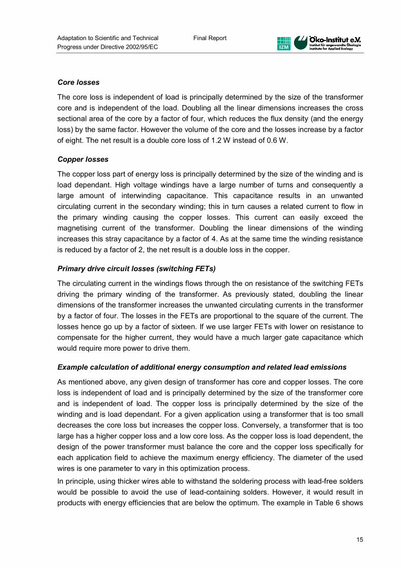
5.1.3.2 Use of thicker wires and efficiency
Asked whether using thicker wires might be a solution, the applicant answered that this mightbe a satisfactory solution for high power units over 30 W output. For high voltage low powerunits using a physically large transformer when only a small one is required would use morecopper and ferrite and increase the core losses, which in turn reduces the energy efficiencyof the unit. Additionally, the applicant says, high voltage units have to be encapsulated. Theuse of a physically larger transformer requires the use of more encapsulation material and alarger enclosure etc.
The applicant provided the following example calculation as evidence for his arguments:
Table 5: Effects of the use of wires thicker than necessary on energy efficiency
Existing transformerwith 0.05 mm wire
Transformer with all dimensionsdoubled to permit the use of0.1 mm wire
Transformer dimensions (mm) 35 × 23 × 15 70 × 46 × 30Core losses 0.6 W 1.2 WCopper losses 0.2 W 0.4 WPrimary drive circuit losses(switching FETs)
0.1 W 1.6 W
Total losses 0.9 W 3.2 W
The calculation is only valid assuming equal use conditions for both products, as the copperlosses depend on the load.
The applicant explains the details of the calculation as follows:
Adaptation to Scientific and TechnicalProgress under Directive 2002/95/EC
Final Report
15
Core losses
The core loss is independent of load is principally determined by the size of the transformercore and is independent of the load. Doubling all the linear dimensions increases the crosssectional area of the core by a factor of four, which reduces the flux density (and the energyloss) by the same factor. However the volume of the core and the losses increase by a factorof eight. The net result is a double core loss of 1.2 W instead of 0.6 W.
Copper losses
The copper loss part of energy loss is principally determined by the size of the winding and isload dependant. High voltage windings have a large number of turns and consequently alarge amount of interwinding capacitance. This capacitance results in an unwantedcirculating current in the secondary winding; this in turn causes a related current to flow inthe primary winding causing the copper losses. This current can easily exceed themagnetising current of the transformer. Doubling the linear dimensions of the windingincreases this stray capacitance by a factor of 4. As at the same time the winding resistanceis reduced by a factor of 2, the net result is a double loss in the copper.
Primary drive circuit losses (switching FETs)
The circulating current in the windings flows through the on resistance of the switching FETsdriving the primary winding of the transformer. As previously stated, doubling the lineardimensions of the transformer increases the unwanted circulating currents in the transformerby a factor of four. The losses in the FETs are proportional to the square of the current. Thelosses hence go up by a factor of sixteen. If we use larger FETs with lower on resistance tocompensate for the higher current, they would have a much larger gate capacitance whichwould require more power to drive them.
Example calculation of additional energy consumption and related lead emissions
As mentioned above, any given design of transformer has core and copper losses. The coreloss is independent of load and is principally determined by the size of the transformer coreand is independent of load. The copper loss is principally determined by the size of thewinding and is load dependant. For a given application using a transformer that is too smalldecreases the core loss but increases the copper loss. Conversely, a transformer that is toolarge has a higher copper loss and a low core loss. As the copper loss is load dependent, thedesign of the power transformer must balance the core and the copper loss specifically foreach application field to achieve the maximum energy efficiency. The diameter of the usedwires is one parameter to vary in this optimization process.
In principle, using thicker wires able to withstand the soldering process with lead-free solderswould be possible to avoid the use of lead-containing solders. However, it would result inproducts with energy efficiencies that are below the optimum. The example in Table 6 shows

_Final Report Adaptation to Scientific and Technical
Progress under Directive 2002/95/EC
16
that going from an optimized power transformer design with 0.05 mm wire to a 0.1 mm wiredesign increases the performance loss for around 260 % from 0.9 W to 3.2 W. Assuming thatthe power transformer is used for 24 h a day, the annual additional energy loss would bearound 20 kWh.
Table 6: Exemplary use scenario and additional energy consumption through lower energyefficiency
Performance Loss (W) Operating time per day (h) Energy loss per year (kWh)Thin wire version 0.9 24 8Thick wire version 3.2 24 28Difference 2.3 20
Assuming that the 0.1 mm wire could be soldered with lead-free solder, around 16 mg of leadwould be saved at the cost of around 20 kWh per year of higher energy consumption.
This additional energy consumption would add up over the years of lifetime of the powertransformer. Additionally, the bigger power transformer would use more materials, and thebigger size itself might be a problem in some applications.
Energy generation itself also causes lead emissions, in particular from coal-fired energyplants. The generation of 1 kWh of electricity in Europe roughly causes around 1 mg of leademissions into air, soil and water (source: reference [1], section 5.1.5). The above scenariowith the 20 kWh of additional energy consumption per year due to the lower energy efficiencywould thus cause around 20 mg of lead per year. This is approximately the same amount oflead as contained in the solder joints of thin wires in one power transformer. Over the lifetimeof the power transformer, the energy-related lead emissions would over-compensate theavoided lead in the power transformer in the above scenario.The copper loss is load dependent, and both the copper and the core loss depend on themode and time of use. If the power transformer is not used 24 h a day, but just 1 h a day, theadditional energy consumption per year is around 1 kWh corresponding to around 1 mg ofenergy-related lead emissions per year. These additional lead emissions would also sum upover the lifetime of the power transformer and at least partially compensate the avoided lead.
The additional use of copper and other materials for power transformers with thicker wiresthan necessary add to the above calculated energy consumption. The production andprocessing of these materials requires energy as well. This could, however, not bequantified, as the respective data were not available.
The additional energy consumption and lead emissions, which are related to this applicationin case the exemption is not granted, cannot be quantified exactly. The above calculationsare all based on the data for one example power transformer, which the applicant hadprovided. Possibly, other design changes might cause other, lower efficiency decreases. Therough estimates, however, show that the additional lead emissions from the lower energy

Adaptation to Scientific and TechnicalProgress under Directive 2002/95/EC
Final Report
17
efficiency would at least partially compensate the around 16 mg of lead per powertransformer, if the manufacturers were forced to use thicker wires than necessary accordingto the example calculations in the tables above.
Countercheck of information with competitors
The consultants contacted four competitors of the applicant to countercheck the correctnessof the information received from the applicant concerning the soldering of thin wires in powertransformers. It was, however, not possible to obtain clear evidence that the applicant’scompetitors have RoHS-compliant solutions for power transformers with thin wires, which arecomparable to the applicant’s power transformers.
Conclusions
The applicant’s information itself is plausible, and he has undertaken efforts to achieveRoHS-compliance. Design changes are possible to avoid the use of thin wires and thusachieve RoHS compliance. This would save around 16 mg of lead per power transformer,but would also increase the product size and the material use, and in particular the energyloss over the product lifetime. The additional energy consumption cannot be quantifiedexactly, as it depends on the specific application. The lead emissions from the additionalenergy consumption, however, would at least partially compensate the lead avoided in thepower transformers.
Rewording of the exemption
The applicant’s proposed wording “SAVBIT solder for soldering of thin copper wires” had tobe altered. The non-RoHS-compliant, lead-containing SAVBIT solder is a name of a productof a specific manufacturer and should not be part of an exemption wording. Further on, theexemption would be too general allowing the use of lead-containing solders for thin wires inany product. The exemption had to be limited to power transformers. No viable, RoHS-compliant options could be proved for the processing of such thin copper wires in powertransformers, and design changes implicate a decrease of energy and material efficiency. Inother products, there might be different conditions and viable design options to achieveRoHS-compliance.
In accordance with the applicant, the wording therefore was changed to:
Lead in solders for the soldering of thin copper wires of 100 µm diameter and less in powertransformers
5.1.4 Final recommendation
It is recommended to grant this exemption. The applicant’s arguments are plausible, andthere is no clear evidence that other manufacturers can solder thin wires of 100 micrometersdiameter and less with RoHS-compliant solders. Design changes to avoid the use of such

_Final Report Adaptation to Scientific and Technical
Progress under Directive 2002/95/EC
18
thin wires are possible, however, at the cost of lower energy efficiency of the powertransformers. The lead emissions linked to the additional energy consumption are in thesame order of magnitude like the amount of lead in the respective solder joints in the powertransformers. The additional lead emissions into the environment would at least partiallycompensate the lead avoided in the power transformers. The exemption would thus be in linewith the requirements of article 5 (1) (b).
The wording of the exemption should be:
Lead in solders for the soldering of thin copper wires of 100 µm diameter and less in powertransformers
5.1.5 References
[1] Frischknecht R., Faist Emmenegger M. (2003): Strommix und Stromnetz. In:Sachbilanzen von Energiesystemen: Grundlagen für den ökologischen Vergleich vonEnergiesystemen und den Einbezug von Energiesystemen in Ökobilanzen für dieSchweiz (Ed. Dones R.). Final report ecoinvent 2000 No. 6, Paul Scherrer Institut
[2] Villigen, Swiss Centre for Life Cycle Inventories, Duebendorf, CH, Online-Versionunder: www.ecoinvent.ch.
5.2 Lead in trimmer potentiometer elements (set 6, request no. 22, TokyoDenshi)
Explanations of specific terms:
Cermet Heat resistant material made of ceramic and sintered metal; here theresistive layer and the ceramic body on which it is sintered upon.
5.2.1 Description of requested exemption
Trimmer potentiometers are variable resistors. They work with a wiper to adjust theresistance of the circuit. They are applied in a wide range of products like e.g. audio-visualequipment, communication equipment, toys and measuring devices, electrical householdappliances.

Adaptation to Scientific and TechnicalProgress under Directive 2002/95/EC
Final Report
19
Figure 3: Example of a trimmer potentiometer (source: Tokyo Denshi)
The trimmer potentiometer elements contain lead as lead oxide in resistive inks. Theresistive ink is composed of silver, lead-ruthenium-oxide and boron trioxide. The applicantsays that currently there is no viable lead-free thickfilm paste available on the market.
Trimmer potentiometer elements weigh between 0.048 g to 0.106 g, with a lead oxidecontent of 0.108 % to 0.35 % corresponding to around 0.052 mg to 0.3 mg of lead oxide pertrimmer potentiometer. The applicant sells around 54,000,000 pieces of cermetpotentiometers. The total amount of lead oxide in the applicant’s products thus is betweenaround three to 16 kg per year. Tokyo Denshi Ltd. assumes that it is currently occupying 1 %of the entire cermet trimmer potentiometer market. The total global annual volume of wouldthen be around 5,400 million of such trimmer potentiometers resulting in around 1,600 kg oflead oxide (PbO) or 1,500 kg of lead consumed in this context.
As cermet trimmer potentiometers come in many different sizes and shapes and there aremillions of manufacturers in the entire industry, it would be difficult to give any accurate figureto the annual volume and thus the amount of lead oxide used in this scope. Yet, we can stillgive a rough estimate based on our annual output and market share. Assuming that TokyoDenshi Ltd. is currently occupying 1% of the entire cermet trimmer potentiometer market, ourannual output of 54 million pcs. (and 16.2 kgs. of lead oxide consumed) projects a globalannual volume of 5,400 million pcs. and thus 1,620 kgs. of lead oxide consumed in thiscontext. We hope this rough estimate may help you address the possible amount of hazardthat could bring about.
The applicant suggests the following wording for the exemption:
Lead in thickfilm pastes for the manufacturing of cermet-based trimmer potentiometerelements

_Final Report Adaptation to Scientific and Technical
Progress under Directive 2002/95/EC
20
5.2.2 Justification for exemption as submitted by applicant and stakeholders
The resistive ink is applied as a thickfilm paste, which is printed on the cermet base as aconductive agent between the wiper and the terminals. After printing, the thickfilm paste issintered onto the cermet base. The lead-oxide in the conductive ink is necessary to evenlymelt the ruthenium-oxide and bond it on the cermet base. Its low sintering temperature below500 °C lowers the curing temperature of the ruthenium-oxide solvent, which enables bondingthe ruthenium oxide to the cermet base without cracking it. Further on, the lead-oxide worksas a bonding agent connecting the aluminium-oxide based cermet and the conductive film oflead-ruthenium oxide. The lead-oxide enhances the adherence of the ruthenium-oxide/ruthenium-dioxide to the cermet base ensuring proper conductivity and the functionalityof the trimmer potentiometer. Compared to other thickfilm resistors, the resistive layer intrimmer potentiometers must have a higher mechanical stability. The wiper runs over theresistor to adjust the resistance, which will cause abrasion of the resistive layer over time ifthe layer does not have sufficient mechanical stability against abrasion. The applicant saysthat on cermets, there is no technically viable substitute to replace the lead-oxide as bondingagent in the thickfilm pastes for the resistive ink.
There is another type of trimmer potentiometers, which are bakelite-based. They can bemanufactured RoHS-compliantly without lead, but are not appropriate for all applications.Firing RuO2 materials on a bakelite film is impossible owing to the high curing temperature.In this connection, only Pb-free carbon can be printed as the resistive track of a bakelite-based potentiometer. This carbon, according to the applicant, is too sensitive to temperatureand humidity changes. The bakelite potentiometers thus can function properly at workingtemperatures of not more than 40°C, while that of a cermet potentiometer can operate attemperatures as high as 70°C or even more.
The applicant states that another important criterion is concerning the working power rating.A cermet (RuO2 resistive track) trimmer potentiometer can withstand power ratings as highas 0.3 W to 0.5 W. A bakelite trimmer potentiometer with carbon track would burn down atsuch power ratings and hence the device circuit went out of order. In this connection, it isthus not uncommon to see that devices including automobile audio/visual equipment,automobile ABS systems, telecom equipment, heaters, negative ion hair clippers, etc. are allusing cermet based (RuO2 resistive track) trimmer potentiometers.
As the consumer market is producing products with more compact sizes, the use of smallersurface-mounted trimmer potentiometers is prevailing. Yet, as the working power rating ofbakelite base trimmer potentiometer would drop in proportion to its size, they cannot providea solution to the power rating requirement of these device circuits. In contrary, the cermetbased trimmer potentiometers with the RuO2 resistive tracks can provide the necessarypower ratings even in surface mounted, meaning miniaturised versions, according to theapplicant. The applicant states that all surface mount trimmer potentiometers are of cermetbase and RuO2 track. Matsushita, Kyocera, Murata, Bourns, etc. trimmer potentiometer
Adaptation to Scientific and TechnicalProgress under Directive 2002/95/EC
Final Report
21
manufacturers are all designing the surface-mounted trimmer potentiometers in cermet baseand RuO2 resistive track.
5.2.3 Critical review of information as submitted by applicant and stakeholders
Electrolux had submitted a stakeholder document opposing the applicant’s exemptionrequest. Electrolux confirms that it uses fully RoHS compliant trimmer potentiometers in itsproducts (see attached stakeholder document “Trimmer_potentiometer_stakeholder.pdf”).The consultation of both the applicant and of Electrolux cleared the situation. It showed thatthe stakeholder had understood the applicant’s exemption request as a request for a generalexemption for lead in trimmer potentiometers. The title of the exemption request in thestakeholder consultation round no. 6 was “Lead in trimmer potentiometers”. The exemptionrequest, however, is limited to the use of lead in cermet-based trimmer potentiometers.
After further investigations at a thickfilm paste manufacturer and manufacturers of trimmerpotentiometers, the applicant’s information could be confirmed. Bakelite-based trimmerpotentiometers are not appropriate for higher power rates and higher moisture. Lead-freethickfilm pastes are not available currently for the use in cermet-based trimmerpotentiometers.
Although for some ranges of resistance, lead-free pastes are possibly available, themechanical resistance against abrasion is not yet high enough to allow a reliable product.
The respective industries so far considered the following exemptions to cover the use of suchlead-containing thickfilm pastes in trimmer potentiometers:
§ No. 5: lead in glass of cathode ray tubes, electronic components and fluorescent tubes,and
§ No. 7: lead in electronic ceramic parts (e.g. piezoelectronic devices).
The applicant was asked whether he was aware of this situation. He replied that he hadchecked the RoHS Directive about this matter before he submitted his proposal. Theapplicant says that it is the ruthenium oxide (RuO2) resistive film printed on the ceramicsheet that contains lead. Tokyo Denshi had consulted a test laboratory technician about theexemption status. The technician replied that he would not agree with the compliance of theresistive film.
The applicant had sought a formal explanation from EU about the inclusion of leadedpotentiometer elements in these exemptions, but the Commission did not take a position.Tokyo Denshi therefore believed that a formal exemption request would be the best to easethe queries in the global electronics market.
The sintering process will not change the chemical form of lead-oxide into another chemicalform. The applicant as well as another manufacturer of thickfilm pastes and vendor ofcermet-based trimmer potentiometers confirmed that

_Final Report Adaptation to Scientific and Technical
Progress under Directive 2002/95/EC
22
the resistive layer is made up of lead ruthenium oxide and lead oxide, which is by nature nota glass. Tokyo Denshi states that it is electrically conductive and the lead oxide added is toserve as an epoxy or bonding agent to get the resistive layer sintered on the ceramic base athigh temperature. According to the applicant, after sintering the resistive track can beremoved by grinding or lapping. Lead oxide itself stays on the cermet base surface but doesnot penetrate into the cermet body. The lead ruthenium oxide (i.e. the resistive layer) couldnot be classified as any glass component, although glass may contain lead also. Lead oxideadded to enable the sintering may be similar to glass.
A further manufacturer of thickfilm pastes and trimmer potentiometers confirmed that lead isavailable as lead-ruthenium-oxide and that the lead is an essential for the resistivityproperties of the cermet material (document “technical fiche20000901.pdf”). He added thatlead also is contained in the glass as lead-boron-silicate and as such is a constituent of theglass components in the cermet layer. The proportionate distribution of lead between thelead in glass and the lead in the resistive layer itself is not known. The stakeholder as well asthe applicant confirms that the resistive layer in principle can be mechanically disjointed bygrinding from the ceramic body and hence consider it as a homogeneous material.
According to the stakeholder, the thickfilm paste contains around 15 % to 20 % of lead inPb2Ru2O7 (lead-ruthenium-oxide, see document “technical fiche20000901.pdf”). Assumingthat the thickfilm paste does not considerably loose weight during the sintering process, thiscorresponds to a lead content of around 8.5 % to 11.4 % in the resistive layer, which isclearly above the maximum threshold of 0.1 % for a RoHS-compliant homogeneous material.
Exemption no. 7 for lead in ceramic parts can be ruled out as both the applicant as allstakeholders involved classify the non-conductive part of the resistive layer or parts thereofas glass, not as ceramic.
In order to be covered by the above exemptions listed in the RoHS Directive, the thickfilmpaste after application, in the finished trimmer potentiometer, would have to be categorizedunder one of the following categories:
1. The resistive layer itself is classified as a glass after the sintering process. It wouldthen be lead in glass of an electronic component and exemption no. 5 would apply.The applicant had ruled out this possibility.
2. The stakeholder classified the resistive layer (excluding the ceramic base) as ahomogeneous material. The stakeholder says that in the sintering process, the lead inthe lead-ruthenium-oxide and the glasses become inseparably connected in theresistive layer. He proposes that the lead in the lead-ruthenium-oxide could beconsidered as a glass, although the homogeneous material itself is not a glass.Exemption no. 5 would then apply.It is not clear, whether this is a viable interpretation of exemption no. 5. The inter-

Adaptation to Scientific and TechnicalProgress under Directive 2002/95/EC
Final Report
23
pretation of the RoHS Directive is beyond the contractor’s competence. Thecontractors’ leave the decision to the respective European entities whether thisinterpretation is permissible.
A new exemption would be justified in line with article 5 (1) (b) of the RoHS Directive if thisapplication is not considered to fall under exemption no. 5
5.2.4 Final recommendation
It is recommended to grant this exemption if this use of lead is not considered to fall undexemption no. 5 allowing the use of lead in glasses of electronic components as laid out inthe previous paragraph under number 2 in section 5.2.3.
The wording of the exemption would be:
Lead in cermet-based trimmer potentiometer elements
5.3 “Cadmium in optoelectronic components” (set 6, request no. 23, MarshallAmplification plc), and “3 year grace period on the use of Cadmium-basedphotoresistors used in professional audio equipment, for the purpose ofinvestigating suitable alternatives and redesigning audio productsaccordingly“ (set 7, request no. 4, Sound Devices)
Marshall Amplification had already requested this exemption in a previous stakeholder round(4th stakeholder consultation, request no. 5). A final recommendation was not pronounced atthat time (see final report from July 2006,http://ec.europa.eu/environment/waste/weee/pdf/rohs_report.pdf). Marshall therefore hassubmitted an almost identical request again in the sixth stakeholder consultation.
Sound Devices submitted an exemption request in the seventh stakeholder consultation,which refers to the use of cadmium in optocouplers in professional audio equipment as well.Both exemption requests target an identical exemption for identical or very similar appli-cations in the audio industry. Hence, they are reviewed together in the following.
5.3.1 Special terms and definitions
Audio limiter A device that permits a high compression to be applied above a setthreshold. It limits the output level from rising much above the setthreshold. Vice versa, it facilitates the maximization of an audio signalto the upper limits of the capabilities of the audio circuitry. Audiolimiters prevent overload distortion, or "clipping". Further on, it allowsfor maximization of the audio level of the desirable audio signalrelative to the audio noise in the floor of the audio signal, an inherentartefact to audio circuitry. (Source: Sound Devices)
_Final Report Adaptation to Scientific and Technical
Progress under Directive 2002/95/EC
24
Clipping An audio signal distortion, which occurs through attempts to increasethe voltage or current in an amplifier beyond its threshold of power.(Source: Sound Devices)
DSP digital signal processing
Gain "...The power increase of a signal, usually expressed in dB."(Received from Sound Devices, source: The Sound ReinforcementHandbook, second addition)
Impedance The electrical impedance Z is the quotient of the complex temporaryvalues, complex amplitudes, or complex effective values of analternate voltage and the current in a network element:
jXRtituZ +==)()(
The resistance R is the real part of impedance, the reactance X theimaginary part. The unit is Ohm, like for the resistance. (Source:Taschenbuch Elektrotechnik, Band 1 Allgemeine Grundlagen, VEBVerlag Technik Berlin, 3. Auflage 1986)
5.3.2 Description of requested exemption
Although not mentioned explicitly in the proposed exemption wordings, the concreteapplication behind both exemption requests is the use of cadmium-containing photoresistorsin optocouplers.
5.3.2.1 Application and function of photoresistors and optocouplers
Optocouplers are used in dynamic processors such as audio compressors, expanders,limiters, and guitar amplifiers for recording studio and live sound music performances. Theyare also applied in portable professional digital audio recorders, where they limit the audioinput AC voltage while recording audio, like for remote news gathering or major motionpictures. In addition, they are applied for voltage limiting in microphone pre-amplifier andaudio mixer products.
The applicants apply for an exemption allowing the continued use of photoresistorscontaining cadmium sulphide. While Marshall wants a general exemption for cadmium inopto-electronic components, Sound Devices limited its exemption request to cadmium usedin photoresistors for professional audio products, which are mainly optocouplers. Dependingon the application different numbers of optocouplers are used in such products. In Marshall’smusic instrument amplifiers, as an example, the different models use between one and nineoptocouplers.

Adaptation to Scientific and TechnicalProgress under Directive 2002/95/EC
Final Report
25
The photoresistors are combined in a single package with an LED to form an optocoupler.The optocoupler allows the transmission of analogue or digital signals between circuits usinglight as signal transmitter. The use of light ensures that the sending and receiving circuits areelectrically unconnected (galvanic isolation).
The sending circuit controls an LED. The light of this LED strikes the surface of the photo-resistor in the receiving circuit. The photoresistor absorbs photons and changes itsresistance according to the intensity of the LED-light it is exposed to. It absorbs the photons,whose energy pushes electrons into the conduction band. The electrons (and their resultinghole partners) conduct, lower the resistance of the photoresistor and thus control theelectrical current in the resistor and the receiving circuit. The resistance of the photoresistorthus gradually decreases with increasing light intensity.
An important use of optocouplers is their application as optical isolators. The sending circuitoperates with a low voltage direct current (5-24 V DC, direct current), the receiving circuitwith a high voltage AC (alternate current, hundreds of volts) current. The optocouplerfacilitates the optical control of such high currents with a low current without electrical contactbetween the two circuits. This physical separation is a safety protection for the user of theproduct. He can only access the low voltage areas of the product, but is protected from thedangerous high voltage circuit.
The semiconductor in the receiving high voltage circuit needs time to arrive at and to returnfrom the higher to the lower resistance state. The resistance of the device falls and returns tohigh resistance over a matter of seconds. This gives the optocoupler device an importantcharacteristic, the dR/dT characteristic (change of resistance over time). The gradual changefrom one state to another one, under a constant LED current, allows the device to switchaudio signals gradually and free from distortion. The dR/dT response is a crucial parameterfor the proper functioning of the product.
PMI provided the information that analogue processors account for approximately 90% of allsales of professional audio processors worldwide. Digital ones account for 10%. The annualworldwide market value of this kind of product is some 400 million US dollars (sources: audiotrade publications, industry publications, US Census Bureau, PMI). This market share isexpected to remain stable for the foreseeable future.
The amount of cadmium used in an optocoupler is around 100 micrograms. Sound Devicessells around 12,000 of such optocouplers in products to Europe resulting in a total amount ofcadmium of around 1.2 g per year in Europe. Total figures for all producers using suchdevices in professional audio equipment are not available. Marshall did not provide anyfigures on this at all.
_Final Report Adaptation to Scientific and Technical
Progress under Directive 2002/95/EC
26
The applicants propose the following wordings for the exemptions:
Cadmium in optoelectronic components (set 6, Marshall)
3-year grace period on the use of cadmium-based photoresistors used in professional audioequipment, for the purpose of investigating suitable alternatives and redesigning audioproducts accordingly (set 7, Sound Devices)
5.3.2.2 Main discussion lines and key stakeholders
This exemption request is complex, as it has different technical argumentation lines andlevels. Additionally, two applicants and several stakeholders were involved in theconsultation and the exemption review process expressing contradicting, conflictingstandpoints.
§ Digital signal processing (DSP) is a new technology and a possible alternative toanalogue technology. DSP does not require optocouplers, and hence does not dependon the use of cadmium-containing photoresistors. Part of the review process therefore iswhether DSP is a viable alternative to the use of the non-RoHS-compliant optocouplers inprofessional audio equipment.The following stakeholders oppose the use of DSP as a viable substitute in professionalaudio equipment:
§ Marshall (manufacturer of professional audio equipment, applicant in stakeholderconsultation 6, Europe)
§ Sound Devices (manufacturer of professional audio equipment, applicant in stakeholderconsultation 7, USA)
§ Casco Silonex (manufacturer of optocouplers, stakeholder, Europe)
§ PMI Audio Inc. (manufacturer of professional audio equipment, stakeholder, Europe)
§ Optocouplers using digital components like silicon-based photocells and phototransistorsinstead of cadmium-containing photoresistors are available on the market. The “OnInstitute for Optical & Electronic Technology”, a stakeholder from China, in the 7thstakeholder consultation submitted a document claiming that digital components canreplace the cadmium-containing photoresistors in optocouplers. It must be clarifiedwhether such devices are a viable option for the professional audio industry.
§ This exemption request also is related to the exemption request no. 21 Cadmiumsulphide photocells from stakeholder consultation no. 2. Applicants had requested anexemption for Cadmium in photocells for dimming lights. The request was recommendednot to be granted as RoHS-compliant alternatives had been available. These alternativesmight as well be suitable substitutes to achieve RoHS-compliance in optocouplers.
§ Another part of the review process is the conflict whether the photoresistors and theoptocouplers, which a manufacturer of optocouplers (Macron) claims to be RoHS-compliant, actually are RoHS-compliant.

Adaptation to Scientific and TechnicalProgress under Directive 2002/95/EC
Final Report
27
Stakeholders involved are:
§ Macron, a Chinese manufacturer of optocouplers, in stakeholder consultation 6 claimedto have a RoHS-compliant photoresistor that can fully replace the cadmium-containing,non-RoHS-compliant photoresistors in optocouplers for audio applications. Macron hassubmitted test results from two laboratories (SGS and RWTT) in the 6th and 7thstakeholder consultation, which, according to Macron, prove the RoHS-compliance of itsphotoresistor/optocouplers. Additionally, Macron has provided supporting letters fromprofessional audio manufacturers confirming that the Macron optocouplers are asubstitute for other manufacturers’ non-RoHS-compliant optocouplers in professionalaudio equipment.
Other stakeholders oppose this view:
§ Casco Silonex submitted test results from a laboratory (ERA) in stakeholder consultation6 and 7, which, according to Casco Silonex, prove that the Macron photo-resistors/optocouplers are not RoHS-compliant.
§ Sound Devices, Casco Silonex and PMI Audio argue that the Macron optocouplerstechnically are not appropriate for the use in the professional audio industry.
§ Finally, it must be reviewed whether the Macron optocouplers, in case that they areRoHS-compliant, actually are a substitute for cadmium-containing photoresistors foroptocouplers in professional audio equipment. Casco Silonex and PMI Audio oppose thisview, while Macron had submitted letters from some of its customers supporting Macron’sposition.
5.3.2.3 Lack of Cooperation from Marshall
Marshall applied for a general exemption of cadmium in opto-electronic components. In orderto clarify this rather broad scope and further open questions the consultant asked theapplicant several times for further information. Although Marshall confirmed the receipt of thequestions and announced to reply, Marshall later on cancelled the further cooperation via e-mail. Against this background the consultant decided to focus only on the almost identicalexemption request no. 4 from Sound Devices (SD) in the 7th stakeholder consultation, butnevertheless took into account the various documents, which several stakeholders hadsubmitted in the 6th stakeholder consultation. Marshall’s wording for a general exemption ofcadmium in opto-electronic components was cancelled, and the contractors’ furtherinvestigations and review of information focused on the use of cadmium in photoresistors forprofessional audio applications, as proposed by Sound Devices.

_Final Report Adaptation to Scientific and Technical
Progress under Directive 2002/95/EC
28
5.3.3 Justification for exemption as submitted by applicant and stakeholders
The following subsections summarize the information from Marshall, Sound Devices, PMIAudio and Casco Silonex submitted in the 6th and 7th stakeholder round and during thereview process.
5.3.3.1 Digital signal processing in professional audio equipment
RoHS-compliant digital signal processing (DSP) based on silicon-technologies, in opposite tothe analogue electronics circuitries using cadmium-based optocouplers, is discussed as analternative. The stakeholders state that digital formats are increasingly used for non-professional applications such as for music compact discs, recording and playback, but thatcurrent digital technology does not reproduce music and sound perfectly, particularly at highand low frequencies. The stakeholders say that although this is acceptable for audioequipment used by consumers, it is unacceptable for professional music recording,publishing and for real time applications like concerts where the sound quality must be anorder of magnitude better than non-professional equipment. The dynamic range of thehuman ear is very wide and it is not possible, using current digital techniques, to accuratelyreproduce sound at very high and very low frequencies. The following paragraphs sum upthe applicants’ and stakeholders’ arguments why DSP is not an alternative to the analoguetechnology using optocouplers with cadmium-based photoresistors for the professional audioindustry.
Conversion from analogue to digital signals
Audio is an AC (alternating current) signal (see Figure 4), so the current must flow throughthe resistive element in both directions, and the resistance therefore must be the same forcurrent travelling in either direction through the resistive element to achieve the linearity ofthe device. According to SD, photodiodes and phototransistors used in optocouplers or inDSP allow current to flow in one direction only and are therefore inherently “non-linear”.
To process an analogue signal digitally, it must be sampled. Its instantaneous amplitude ismeasured at fixed time intervals (the “sampling rate”). While analogue has infinite resolution,the sampling process results in a finite resolution and changes the nature of the audio signal.Although the digital signal can be converted back to analogue, digitalization is anapproximation process of the sampled signal to the original input signal. The faster theanalogue input waveform changes, the worse the approximation.

Adaptation to Scientific and TechnicalProgress under Directive 2002/95/EC
Final Report
29
Figure 4: Digitalisation of an analogue waveform (source: PMI Audio)
Higher sampling rates reduce the error and give a better approximation, but, according toPMI Audio, remain an approximation only, while professional audio equipment must beoptimised to reproduce the original input sound. PMI Audio quotes the Nyquist theory. Toavoid quantification errors, the sampling frequency must be at least twice the maximumfrequency of up to 100 kHz, which is actually necessary to faithfully reproduce the 20 kHzaudio spectrum. Only the recent “DVD” standard with its sampling frequency of 192 kHzmeets this criterion.
PMI Audio says that another source of signal information loss is that digital circuitry operatesat between 3 Volts and 5 Volts, whereas analogue circuitry is ten times that. Hence ananalogue signal must be attenuated by a factor of ten (20 dB) in order to be digitalised. Theprocess of attenuation inevitably looses some information and increases noise slightly, dueto the additional components required. Conversion back to analogue also worsens noise anddistortion, because of the 20 dB of amplification required.
Digital signal processing
Once the analogue audio signal is digitalised, it must be processed. The amplitude of anaudio signal with a resolution of 0.1 dB is a reasonable requirement for a professional audioprocessor. This is easy to achieve in the analogue domain, PMI says, but not in the digitalone. A gain reduction of 0.1 dB requires the use of non-integer, floating-point arithmetic. Thismeans that the digital word length used for computation needs to be much greater than thatneeded for sampling. ADC- (analogue-to-digital conversion) and DAC-unites (digital-to-analogue conversion) can use 24 bits to achieve a dynamic range of 140 dB, whereas theDSP needs at least 64 bits, even to approach an acceptable emulation of an analogueprocessor. Commonly available DSPs are currently 32-bit.

_Final Report Adaptation to Scientific and Technical
Progress under Directive 2002/95/EC
30
The digitalised audio signal is subjected to many stages of approximation, which produceunsatisfying results regardless of the accuracy of the emulation algorithms. Emulation furtheris complicated by the complex response of the photocell that is being emulated. All thesefactors result in approximation errors, which all reduce the sonic accuracy of the DSP systemcompared with an analogue one.
PMI put forward that measurable differences between analogue and digital systems veryoften could not be revealed by simple measurements using simple test equipment.Commonly measured parameters, such as noise and harmonic distortion of a steady-statesignal, actually reveal very little about how an audio signal will “sound”. Analysis performedby the human brain is far more sophisticated. An appropriate method to compare thesimilarity of the analogously and digitally processed signals is the “invert and add” method.One of the two signals, either the original analogue or the processed digital one, is invertedand summed (mixed) with the other. Providing the two signals have identical amplitude, thetwo signals should extinguish each other such that nothing audible remains. Any residuerepresents the inaccuracy of the DSP in emulating the analogue process. In PMI’sexperience, this method always reveals clear differences between the analogue and digitalaudio signals.
“Analogue sounds better than digital” has also been validated by the discipline of studyknown as “Psychoacoustics”. This uses the methods of experimental psychology, such as“double blind” listening tests and statistical analysis(http://en.wikipedia.org/wiki/Analog_sound_vs._digital_sound#Subjective_evaluation; sourcecited by PMI Audio).
Latency
Conversion from analogue to digital, DSP processing and conversion back from digital toanalogue takes time known as latency. Typical latencies for current digital technologies are:
Analogue to digital 1 to 2 milliseconds
DSP 3 to 4 milliseconds
Digital to analogue 1 to 2 milliseconds
Total: 5 to 8 milliseconds
According to PMI, studies have shown that a good drummer can be time-accurate to 150microseconds. Simple changes to the “mood” of playing, for example from “rock-steady” to“laid-back”, involve a change in timing of just 1 millisecond of hits on a snare drum. A latencyof several milliseconds makes it impossible to play along with Digital Audio Processors inreal time. PMI states that this is completely unacceptable in many situations within theprofessional recording and broadcast industries. Digital audio processing would require a

Adaptation to Scientific and TechnicalProgress under Directive 2002/95/EC
Final Report
31
hundred-fold increase in processing speed to remove this objection. At the current state ofthe art, this is not achievable, according to PMI.
Environmental Implications of DSP and shorter usage time of portable equipment
The stakeholders say that a DSP-based system contains much more active components.Any digital system also requires analogue input and output filter circuitry, which alone usesmore components than the entire circuitry of an analogue device. Figure 5 shows a DSPcircuit and a Joemeek compressor (see paragraph “Tradition” in section 5.3.3.2) inapproximately the same scale.
Figure 5: Typical twin-board DSP module (left) and Joemeek analogue compressor (right) (source:PMI Audio)
The analogue Joemeek version (right) uses three 8-pin chips, while the digital "equivalent"uses three 144-pin chips on the upper DSP board alone. All the circuitry for analogue todigital and the digital to analogue conversion and filtering is on the lower board. Thestakeholders say that the manufacturing of the digital chips and the larger printed circuitboard with far more soldered joints requires more energy and material, but did not providequantitative data.
During operation, photoresistor-controlled circuits do not consume energy when they are notoperating. According to PMI, a Joemeek compressor circuit as an example for analoguesignal processing consumes less than 0.5 W, while a digital system typically consumes 5 Wcontinuously, whether it is under operation or not. The power consumption and heatproduction of a DSP-unit increases with the processing power of the DSP.
According to Sound Devices (SD), energy consumption is a critical parameter in particular forportable devices operating on battery power. Analogue portable audio mixers are designedfor extremely low power consumption to maximize battery life in the film and newsgatheringindustries. Using DSP in such devices decrease the battery-life performance and the use

_Final Report Adaptation to Scientific and Technical
Progress under Directive 2002/95/EC
32
time of the portable devices in field shortens, while battery consumption and wastesincrease.
Sound Devices says that due to their simplicity compared to DSP units, the use ofoptocouplers with cadmium sulphide photoresistors enable products with minimum size andweight for the broadcast and film markets. According to SD, these light and small productsprovide a substantial health benefit as Location Audio engineers carry them over theirshoulder for a full workday. It was not uncommon for a Location Audio Engineer to retire atage 40 to 45 due to typically spinal ailments. Reduction in weight by up to 50% of audio toolsin recent years has improved the health and extended the careers of these Audio Engineers.
5.3.3.2 Specific properties of cadmium-based photoresistors for optocouplers
The stakeholders and applicants explain which unique properties of cadmium-basedoptocouplers make them indispensable for the audio industry. The following explanations area summary of the applicant’s and stakeholders arguments.
Suppression of electrical noise and low distortion
A crucial property of cadmium-based photoresistors for optocouplers in professional audioequipment is the change of resistance over time as a reaction to light, the dR/dTcharacteristics, or the inherent fast-attack/slow-release characteristic. The “attack time” refersto the time it takes for the photo-resistor to go from a high to a low resistance, and vice-versafor “release time”. The dR/dT-characteristics can be adapted to the specific requirements ofthe respective application. A typical attack time is 50 ms, a typical release time 500 ms.
The attack time of around 50 ms is fast enough to allow a distortion-free transfer of signalswithout e.g. blurring spoken words. On the other hand, the attack time is slow enough tosuppress electrical noise and inharmonic distortions from the sending circuit generating shortflashes of light from the LED. Such short flashes of light will not affect the resistance of thephotoresistor. Electrical noise in the sending circuit is thus eliminated in the receiving circuit.
Audio equipment must reliably represent the material being mixed or recorded without addingany electrically created noise or distortion. Inharmonic distortion examples include whitenoise, digital pulses, initial overdriving, and electrical noises generated outside of the audiocircuitry.
The long release time of photoresistors keeps the harmonic distortion low. The gain onlyaffects the amplitude of the waveform without affecting the basic shape of the waveform,which would result in harmonic distortions. Linearity is another typical property ofoptocouplers with cadmium-based photoresistors. Their electrical response is a regular linearfunction of the input light level. The linearity of the optocoupler translates directly intominimization of harmonic distortion.
Phototransistors and diodes as a possible replacement of cadmium-based photoresistors inoptocouplers do not have the unique dR/dT characteristics and their response is not linear,

Adaptation to Scientific and TechnicalProgress under Directive 2002/95/EC
Final Report
33
according to the applicant Sound Devices. They also react with resistance changes to light.The conduction of the silicon device occurs in the moment the AC signal’s amplitudeexceeds the photovoltaic voltage drop. The silicon device then conducts, which causes anunacceptable deformation of the audio signal. Further, audio signals are AC signals. Assilicon-based components like photodiodes and phototransistors allow current to flow throughit in one direction only, the audio signal deformed. Electrical noise and distortions are noteliminated, or it requires considerable additional circuitry to achieve a quality of the audiosignals, which is still below the quality of the audio signal from cadmium-based optocouplers.Optocouplers for professional audio applications need components with continuouslyvariable resistance providing a wide linear and consistent resistance change.
Dynamic range
Optocouplers with cadmium-based photoresistors can respond to a large range of lightlevels. Typically they react to light levels from 0.02 Lux to over 10,000 Lux with an equallylarge range of resistance. Resistance values are typically from 2 ohm to 50 Mega-ohm.
Professional high quality audio applications like audio limiters for field use require such highdynamic ranges to handle the broad range of audio stimuli: capturing wildlife sounds such asbirds at 50 meters when a deer approaches at 10 meters, or if a gun fires at 10 meters. Theloud sounds should be undistorted, and at the same time the quiet sound of the birds shouldnot be clouded by noise produced by the audio circuitry. The nominal sound levels can be asmuch as 100 dB apart. Optocouplers based on photodiodes cannot provide the necessaryrange of light sensitivity levels and reactive resistance changes, as the next table shows.
Table 7: Dynamic range of main photocell types
Photocell type Dynamic range; light sensitivity fortypical devices, actual vales dependon design but range is notsignificantly affected
Wavelength response
CsS/CdSe 0.02 Lux - >10,000 Lux 400 – 700 nm
Single crystal silicon 100 Lux – 1000 Lux ~400 – 1200 nm
Amorphous silicon (a-Si) 200 Lux – 600 Lux <400 nm – ~820 nm
GaAs, GaAlAs 100 – 1000 Lux ~ 600 – ~950 nm
Source: Casco Silonex document no. 8 in references, section 5.3.6
Low cost and short development time
Optocouplers are less expensive than other analogue circuit or DSP-based options. Theyallow cost-effective and, due to their simplicity, quick solutions with short development times.

_Final Report Adaptation to Scientific and Technical
Progress under Directive 2002/95/EC
34
According to PMI, DSP technologies are around 20 times more expensive than the existinganalogue circuitry, which makes DSP commercially unacceptable.
Tradition
PMI says that its products are based on the “Joemeek Compressor Circuit”, a classic piece ofaudio engineering using a cadmium sulphide photoresistor pioneered by record producer JoeMeek in the 1960's. PMI puts forward that the technology itself is a brand and stands for atradition and as such cannot be replaced, even if it would be technologically possible toimitate the effect with RoHS-compliant devices. Should the exemption not be granted, anentire tradition of technology would be put beyond reach of manufacturers and consumers,both amateur and professional, and would cause enormous damage to the viability of PMI’sand other manufacturers’ business. It would also give the rest of the world an unfairadvantage over the EU in the field of music recording and production.
5.3.3.3 Sound Devices’ justification for the 3-year exemption period
Sound Devices asks for a three-year exemption for the use of cadmium in photoresistors inprofessional audio equipment. SD says that analogue circuitry simulating the performance ofan optocoupler is possible, as due to the ongoing miniaturization the sizes of electricalcomponents are shrinking and power requirements have been going down. The applicantforesees a strong future potential that if he is given appropriate design time, he can produceRoHS-compliant products with alternative circuits replacing the non-RoHS-compliantoptocouplers within the next three years.
In February 2007, Sound Devices first attempted the implementation in a prototype ofportable microphone preamplifier. It was not successful but showed promise. After two moredesign changes the applicant says that the circuit is close to being suitable for portableprofessional audio, and he believes that he can start the integration into products in February2008. Sound Devices says that each product requires a unique design to accommodate thevariations in the audio circuitry. Sound Devices says that it has ten other existing productsthat require modifications to this new circuit design, or a complete product redesign for theuse with the new limiter circuit concept replacing the non-RoHS-compliant optocouplers.According to the applicant, the redesign for all of these products would require a minimum oftwo years, and a maximum of three years depending on the number of PC Board revisionsrequired to produce acceptable results.

Adaptation to Scientific and TechnicalProgress under Directive 2002/95/EC
Final Report
35
5.3.4 Critical review of information as submitted by applicant and stakeholders
5.3.4.1 Overview on different test results for RoHS-compliance of Macron photo-resistors and role in the review process
There are different test results available leading to different conclusions about the RoHS-compliance of Macron photoresistors. To some extent, these results diverge as a result ofdifferent interpretation in the understanding of “homogeneous material”. In this context, itmust be taken into account that neither the Commission nor the contractor, but only theEuropean Court of Justice decides about the interpretation of the RoHS Directive. Againstthis background, the contractors solely present the test procedures, results, andimplausibilities, as far as possible.
Macron presents four models of photoresistors, which also contain cadmium. According toMacron, the concentration of cadmium in the homogeneous material of these photoresistorsremains below 0.01 % of weight, which is the maximum allowed cadmium level for RoHS-compliance.
The supporters of the exemption request challenge Macron’s claim that these photoresistorsfor optocouplers are RoHS-compliant. Both the supporters of the exemption request andMacron have submitted several test reports dealing with the RoHS compliance of the Macrondevices. The Macron test reports confirm RoHS-compliance; the opponents’ test reports theopposite.
The following sections show an overview of the most important tests and their results. Fordetailed information, please refer to Annex II.
Macron test reports
Macron had submitted testing documents in the 6th stakeholder consultation confirming theRoHS-compliance of the tested photoresistors and optocouplers. None of the reports,however, clearly indicated which photoresistors and optocouplers had been tested andhence are not further reviewed in this subchapter. To allow an overview of the differenttesting approaches and the chronological submission of the different test reports by bothMacron and Casco Silonex as a reaction to each other, all tests and their results aredescribed in detail in Annex II.
In the review process following the seventh stakeholder consultation, Macron submitted anew test report (document no. 12 in references, section 5.3.6). The report explains thattraditional photocells usually contain a layer of CdS/CdSe which acts as a photosensitivelayer. Macron says it uses less cadmium it mixes cadmium into the ceramic base, whichallows the ceramic base to have photosensitive function. The testing laboratory refers to thisspecific ceramic as “white ceramic” and considers it as homogeneous material, as thefollowing figure underpins.

_Final Report Adaptation to Scientific and Technical
Progress under Directive 2002/95/EC
36
Figure 6: Physical appearance and homogeneous materials in Macron photoresistors (source: RWTTtest report, document no. 12 in references in section 5.3.6)
The report specifies the tested product as Macron’s MI 1210CLA-R (A-type), which accordingto Macron has the highest content of cadmium to achieve a high photosensitivity. Thefollowing table shows the sampling procedure and the cadmium content for each of theobtained samples. The samples were analyzed using XRF analysis.
Table 8: Sampling and XRF analysis results of obtained samples (accuracy ± 50 ppm)

Adaptation to Scientific and TechnicalProgress under Directive 2002/95/EC
Final Report
37
Source: Macron test report/RWTT, document no. 12, section 5.3.6

_Final Report Adaptation to Scientific and Technical
Progress under Directive 2002/95/EC
38
The testing laboratory conducted a total of ten abrasions, but did not detect any cadmium inany of the further abrasions after the fifth one.
According to these test results, only the last bit of transparent layer (material of 5th abrasion)would contain 0.0031 % (31.1 ppm) of cadmium, which is below the maximum allowed levelof 0.01 % for RoHS compliance. The photoresistor would thus be RoHS-compliant. Fordetails refer to document no. 12 in references in section 5.3.6.
Macron was asked to explain the results. The cadmium, according to the process descriptionin the test report, is mixed into the ceramic base. The test result, however, indicates nodetectable cadmium in the ceramic base, but only in the last bit of abraded transparentplastic. Macron explained that the cadmium was detected in the 5th abrasion of thetransparent layer because RWTT might have abraded parts of the white ceramic with the lastbit of transparent layer. There is no cadmium in the transparent layer, according to Macron,but the cadmium concentration should be higher nearer to the photo-sensitive surface of theceramic and it was therefore detected with the first abrasions of the white ceramic.
Macron further on states the test result might as well have to do with the XRF analysis. TheXRF analysis deviates within ± 50 ppm (± 0.005%), as also mentioned in the ERA report.Macron states that its photosensitive ceramic contains cadmium under the surface layer, too,but that it cannot be detected due to the inaccuracy of the XRF analysis.
In another statement, Macron says that for each of its optocouplers, a total of around 80 ppmof CdS and CdSe referring to the weight of the solid ceramic is added into the ceramic liquidfor mixing. For further details, please refer to Annex II.
ERA test reports
The most important ERA test by the order of Casco Silonex was submitted in the reviewprocess following the 7th stakeholder consultation (document no. 11, section 5.3.6). Thefollowing Macron devices had been tested:
§ MI 1210CLA-R (type “A”)
§ MI 1210CLB-R (type “B”)
§ MI 1210CLH-R (type “C”)
The above models are the models of the Macron MI1210CL-R series, for which Macronclaims RoHS compliance. The “C”-denomination of the last of the three series, theMI1210CLH-R, however, is not congruent with Macron’s information. According to Macron,this is the “H”-series, and there is no information from Macron whether a “C”-series actuallyexists. In the ERA test report, the MI 1210CLH-R model is sometimes addressed as “C”-type,sometimes as “H”-type (e.g. in Table 9).

Adaptation to Scientific and TechnicalProgress under Directive 2002/95/EC
Final Report
39
Figure 7: Image of Macron photocell (source: ERA, see document 7 in references, section 5.3.6)
ERA challenges the homogeneous material definition of the RWTT test reports. ERA saysthat the “white ceramic” (sample 1 in the Macron test report) can be mechanically disjointedinto two homogeneous materials:
§ the ceramic base
§ photosensitive layer containing cadmium and the metallisation (cannot be mechanicallydisjointed from cadmium layer)
ERA describes that the light dependent resistors have coatings of a transparent gel over athin metal mask that defines the resistor path which is made of the photosensitive material.”
Figure 8: Light dependent resistors from Macron optocoupler type “A”, type “B” and type “C” (left toright) (source: ERA, see reference document no. 11, section 5.3.6)
ERA scraped off the transparent gel with a surgical scalpel. The very thin metal layer couldnot be separated from the photosensitive layer. The photosensitive layer with metal maskwas removed from the substrate from between the metal pins as one material with thescalpel.

_Final Report Adaptation to Scientific and Technical
Progress under Directive 2002/95/EC
40
Figure 9: Light dependent resistors from Macron optocoupler type “A”, “B”, “C” (left to right) after thegel and photosensitive material coatings had been removed (source: ERA, document no. 11,section 5.3.6)
The scraped off material was analyzed with a Scanning Electron Microscope (SEM) andenergy dispersive X-ray (EDX) analysis.
Table 9: SEM/EDX analysis of photosensitive coating from Macron optocouplers
Results (weight percent) Comments
“A“ Cadmium 60,6 %, sulphur 15,5%, selenium 5,5 % This material is cadmium sulphide/selenide
“B“ Cadmium 70 %, sulphur 18,4 %, selenium 4,1 % This material is cadmium sulphide/selenide
“H“ Cadmium 58,2 %, sulphur 15,1 % selenium 2,3 % This material is cadmium sulphide/selenide
(Source: ERA, document no. 11, section 5.3.6 )
ERA explains that the figures in the table for the cadmium-containing elements do not add upto 100% because small amounts of impurities from the gel coating (carbon and oxygen) andthe alumina substrate (aluminium and oxygen) have not been included.
According to the test results in Table 9, the cadmium content in the analyzed Macronphotoresistors would be clearly above 0.01 %. The optocouplers would thus not be RoHS-compliant. For details, refer to document no. 11 in references, section 5.3.6.
Conclusions
The test reports submitted by Macron and Casco Silonex arrive at contradicting statementson the RoHS-compliance of the Macron photoresistors and optocouplers. The consultantcannot take a position on the correctness of the testing and the test results, as mentionedbefore.
The question whether the tested Macron photoresistors actually are a technically appropriatesubstitute for the other, non-RoHS-compliant photoresistors in optocouplers of professionalaudio equipment thus becomes obsolete. The potential users of such devices are in the best

Adaptation to Scientific and TechnicalProgress under Directive 2002/95/EC
Final Report
41
position to decide whether or not the Macron products are a viable option for their specificprofessional audio applications.
5.3.4.2 Non-cadmium-based optocouplers as alternative to cadmium-containingoptocouplers
A stakeholder from China, the ON institute, had submitted a document opposing theexemption of cadmium in optoelectronic components (see document 10 in references,section 5.3.6). The stakeholder reasons that appropriate RoHS-compliant optocouplers areavailable on the market and lists examples:
§ PC817 from different manufacturers,
§ HCNR200 (USA, Avagotech, www.avagotech.com),
§ TIL300 (USA, Burr Brown Inc.).
A crosscheck on the internet showed that the Burr Brown component is no longer availableon the market. The Avagotech component, however, was found on the manufacturer’swebsite. It is an optocoupler, which does not use photoresistors, but photodiodes. Whetherthis component is actually RoHS-compliant was not clear from the information available onthe manufacturer’s website. It was not possible to obtain a list with RoHS-compliantoptocouplers including the necessary application-relevant technical data.
Nevertheless, Sound Devices was asked to explain why such optocouplers are notappropriate for its products. Sound Devices explained that audio is an AC (alternatingcurrent) signal, so current must flow through the resistive element in both directions, and theresistance therefore must be the same for current travelling in either direction through theresistive element. Sound Devices says that this is the essence of what is called the “linearity”of the device. According to SD, photodiodes and phototransistors allow current to flow in onedirection only and are therefore inherently “non-linear”, thus making them inapplicable forimplementation as resistive elements around an operational amplifier. Further information onsilicon-based elements as substitutes for cadmium-based photoresistors in optocouplers wasalready explained in subchapter 5.3.3.2.
This exemption request is also related to the exemption request no. 21 Cadmium sulphidephotocells from stakeholder consultation no. 2. Applicants had requested an exemption forcadmium in photocells for dimming lights. The request was recommended not to be grantedas RoHS-compliant alternatives had been available. These alternatives were presented toSound Devices as well in order to check whether they might be a possible solution or part ofa solution. Sound Devices replied that the devices are not variable resistors, but only lightsensors with a current output, which cannot be used in an audio gain stage.
They cannot be used to achieve the required properties of cadmium-based photoresistors inoptocouplers as described in chapter 5.3.3.2.

_Final Report Adaptation to Scientific and Technical
Progress under Directive 2002/95/EC
42
5.3.5 Final recommendation
Apart from some economical arguments and the argument that a traditional circuit like theJoemeek circuit must be allowed an exemption, the applicants and stakeholders technicaland environmental arguments justifying an exemption.
The applicants and stakeholders explained that DSP at the current state of technology is notan alternative to replace analogue sound processing circuits in order to avoid the use ofcadmium-based optocouplers in all professional audio applications. The applicants andstakeholders are not fully in line where DSP might already be used today and where not.They showed, however, that forcing the professional audio industry to switch to DSP or otherpossible alternatives would arise technical and environmental impacts. Increased energyconsumption linked to shorter product battery times in case of in-field-use devices, use ofmore and more complex electronics components and printed wiring board materials, andpossibly heavier products burdening the health of workers in in-field-use of these products.
Technically, the use of DSP in many cases will not allow the sound quality sufficing the highdemands of professional audio applications as with analogue technologies based oncadmium-containing optocouplers. The same applies to the use of alternative optocouplersthat work with photodiodes or other RoHS-compliant, photosensitive elements as substitutesfor the basic, light-depending functionality of cadmium-dependent photoresistors.
The above technical and environmental drawbacks must be weighted against the use ofminor amounts of cadmium. Sound Devices ships around 1 g of cadmium into Europeannually. The applicants did not provide total figures for Europe. Assuming, however, that thetotal amount is 1,000 times higher, it is around 1 kg of cadmium involved in the requestedexemption in Europe.
The contradicting RoHS-compliance tests did not allow assessing whether the Macroncadmium-based photoresistors contain cadmium below the allowed threshold level of 0.01 %and therefore are RoHS-compliant. The technical properties of the Macron componentsregarding their appropriateness as a substitute for non-RoHS-compliant photoresistors werenot assessed, as the RoHS-compliance could not be decided either. It is thus currently notpossible to recommend a RoHS-compliant, cadmium-based alternative for optocouplers.
The applicants and stakeholders have different opinions about the future possibilities of DSPand alternative analogue technologies to substitute the cadmium-dependent analoguetechnologies. Sound Devices presented a roadmap suggesting that a RoHS-compliantsolution is possible within three years and proposes an exemption limited to three yearsstarting in beginning of 2006.
Taking into account all the facts reviewed the contractors assume that the technical andenvironmental arguments might suffice the requirements of article 5 (1) (b). As for someapplications, RoHS-compliant alternatives like DSP might be a solution; the exemption could

Adaptation to Scientific and TechnicalProgress under Directive 2002/95/EC
Final Report
43
be limited to specific applications, which would require a further investigation and informationgathering round to assess the products where technically viable RoHS-compliant alternativesare possible and where not. The environmental implications, however, at the current status oftechnology might allow a general exemption for the use of cadmium in optocouplers forprofessional audio equipment providing that the Commission gives higher priority to theseenvironmental and possible health implications than to the avoidance of a maximum of 1 kgof cadmium, probably less.
In this case, the contractors recommend granting an exemption with the following wording,which was changed from the original wording in accordance with the applicant SoundDevices:
Cadmium in photoresistors for optocouplers applied in professional audio equipment until 31December 2009.
5.3.6 References
The below files are attached to this report.
The following documents are stakeholder documents submitted in the 6th and 7th stakeholderconsultation rounds:
1. Stakeholder document “Attachment 1 SGS Photocell report1.jpg” submitted by MacronElectronics Limited (testing laboratory: SGS),
2. Stakeholder document “Attachment 1 SGS Photocell report2.jpg” submitted by MacronElectronics Limited (testing laboratory: SGS),
3. Stakeholder document “Attachment 3 SGS Optocoupler report1.jpg” submitted byMacron Electronics Limited (testing laboratory: SGS),
4. Stakeholder document “Attachment 3 SGS Optocoupler report2.jpg” submitted byMacron Electronics Limited (testing laboratory: SGS),
5. Stakeholder document “RoHS_and_WEEE_Macron_Photocell_RT069686.pdf”submitted by Macron Electronics Limited (testing laboratory: RWTT),
6. Stakeholder document “RoHS_and_WEEE_Macron_Optical_Isolator_RT069701.pdf”submitted by Macron Electronics Limited (testing laboratory: RWTT),
7. Stakeholder document “Silonex Macron RoHS status letter.pdf” submitted by Silonex(testing laboratory: ERA),
8. Stakeholder document “Marshall_Marshall support letter 01 08 07A-1.doc”, submittedby Marshall,
9. Stakeholder document “PMI Support Cadmium in Optocouplers.htm” submitted by PMIAudio Inc.,
10. Stakeholder document “About Cd.doc” submitted by the On Institute for Optical &Electronic Technology.

_Final Report Adaptation to Scientific and Technical
Progress under Directive 2002/95/EC
44
The next documents were submitted or referenced in documents submitted to Ökoinstitutand Fraunhofer IZM during the RoHS exemption review process:
11. Report “ERA opto coupler analysis Aug 2007-new.pdf”, received in August 2007 via e-mail from Euan Davidson, Chromotechnic Ltd. (testing laboratory: ERA),
12. Report “RT079366_R2.pdf”, received in August 2007 via e-mail from Stephen Leung,Macron.
13. RoHS Enforcement Guidance Document, Version 1 – issued May 2006,(http://www.rohs.gov.uk/Docs/Links/RoHS%20Enforcement%20Guidance%20Document%20-%20v.1%20May%202006.pdf); the document is informative and advisory, buthas no legal authority.
5.4 “Pb and Cd in printing inks for the application of enamel on glasses, suchas borosilicate and soda lime glasses” (set 7, request no. 1a, ELCF)
5.4.1 Requested exemption
The European Lamp Companies Federation (ELCF) has submitted this request for a changein wording of an existing exemption: entry no. 21 of the Annex to the RoHS Directive reads“Lead and cadmium in printing inks for the application of enamels on borosilicate glass”.ELCF requests to have following new wording for entry no. 21:
“Lead and cadmium in printing inks for the application of enamel on glasses, such asborosilicate and soda lime glasses.”
According to the applicant, lead is used in printing inks on parts of the outer surface of lamps(e.g. fluorescent lamps). These markings are essential for product identification, asrequested by safety standards. The marking has several functions, during entire life cycle:
§ To identify the producer,
§ to identify lamp type and wattage, which is relevant for safety, correct lamp replacementand recycling,
§ CE, WEEE marking.
The applicant states:
“Product identification is required by the relevant product safety standards, which are thebasis of the CE Marking according to the LVD Directive (2006/95/EC). Product identificationmust be legible for the consumer or other stakeholders during the entire life cycle of theproduct (safety, replacement, recycling etc.)
Intensive heat and light during lamp operations result in quality challenges for the marking ofa lamp. Some luminaries, state a maximum wattage in order to avoid excessive heat. If amark is not properly legible for the user, the user might place the wrong lamp into a luminaire

Adaptation to Scientific and TechnicalProgress under Directive 2002/95/EC
Final Report
45
with the consequence of a high safety risk. […] Moreover, marking of lamps at the end of lifeis also required by the WEEE Directive.”
The amount of lead for the marking is about 0,25 mg for a normal fluorescent lamp (i.e. orderof 1 ppm of glass tube by weight) and 1 mg for a relatively big mark on an incandescentlamp. The lead-based marking contains as such 20 % lead-oxide. Total EU market quantityfor this application is assumed to be 1-2 tons of lead per year. For the marking of lamps,ELCF Member Companies do not need mercury.
5.4.2 Summary of justification for exemption
The applicant justifies his request for exemption with juridical and technical arguments:
§ Until now, RoHS compliance is given since ELCF considers the marking as being part ofthe glass1 and thus considers the marked glass as homogeneous material containinglead below the maximum concentration limit of 0,1% by weight.
§ Since the European Special Glass Association (ESGA) had submitted a request forexemption (cf.http://circa.europa.eu/Public/irc/env/rohs/library?l=/requests_exemptions/crystal_crystal_crystal_&vm=detailed&sb=Title) under a previous stakeholder consultation leading toentry no. 21 in the RoHS Annex, ELCF claims to also need an exemption for the sametype of application in order to have legal certainty and thus requests the current wordingto be enlarged to soda lime glasses.
§ “ELCF Member Companies are committed to phase-out the use of hazardous substanceslike lead”. The applicant claims that results of tests showed that using lead-free printinginks on lamps does not meet the above-mentioned requirements.
§ “To some extent elimination of lead in marking has been shown to be feasible for somekind of lamps but not for all products. […] Especially for long-life products […] or productshaving a hot external surface during lamps operation […], attempts to eliminate lead inmarking have not yet been successful.” The applicant has not provided an exhaustive listof applications concerned by this statement.
§ “Several years” would be needed by the applicant to completely substitute lead in theconcerned application.
§ A critical review of the documents made available by the applicant lead to the followingobservations and conclusions:
§ ELCF did not take the opportunity to participate in the initial discussion around ESGA’sinitial exemption request; no objection has been received at that time concerning ESGA’s
1 „In the marking process the lead oxide based printing ink is heated that results in a moulding or meltingdiffusion process with the glass surface.“ The mark is then “intrinsically” bonded to the glass.

_Final Report Adaptation to Scientific and Technical
Progress under Directive 2002/95/EC
46
interpretation of the fact that glass marked with lead-containing printing inks cannot beconsidered a homogeneous material.
§ ELCF uses the same argumentation concerning technical impracticability of leadsubstitution in glass marking as ESGA did; thus this argumentation line is consistent.
§ ELCF shows some inconsistency when stating on the one hand that marked glasscontaining lead from the printing ink is considered a homogeneous material and on theother hand states that “one has to resort to intensive abrasion or chemical dissolution toseparate the from the glass”, i.e. a statement that includes both definitions ofhomogeneous and not homogeneous material. However, the official position publishedon ELCF’s website is that “the mark becomes part of the lamp glass. Therefore themarked glass is considered as a homogeneous material below the maximumconcentration limit of 0.1% by weight.2”
§ It is not known to the contractor whether ESGA and other relevant stakeholders would inthe meantime agree to this position. A separate consultation would be needed to gatherinformation and evaluate this aspect.
§ There are only two conclusions possible from the above-mentioned argumentation:
1. The current exemption under entry no. 21 of the RoHS Annex should be deletedsince all relevant stakeholders could now agree on the fact that the marked glass is tobe considered a homogeneous material OR
2. The current entry no. 21 of the RoHS Annex should be enlarged to soda lime glassessince the same justification applies to soda lime glass as to borosilicate glass.
5.4.3 Final recommendation
With a view to simplify EU regulations, deleting an exemption from the Annex is ratherrecommendable. However, since it is not known whether relevant stakeholders would as bytoday agree to ELCF’s interpretation on marked glass as being a homogeneous material, it isrecommended to grant this exemption and to thus change the existing wording of entry no.21 of the RoHS Annex as follows:
“Lead and cadmium in printing inks for the application of enamel on glasses, such asborosilicate and soda lime glasses.”
However, it is strongly recommended to review this exemption in the context of the upcomingreview of the RoHS Annex including the following aspects:
§ Do ESGA and ELCF represent all relevant stakeholders in this field of application orwhich other relevant stakeholders can be identified?
2 See: http://www.elcfed.org/uploads/documents/-7-elc_guidance_document_on_rohs_market_surveillance.pdf

Adaptation to Scientific and TechnicalProgress under Directive 2002/95/EC
Final Report
47
§ Can all relevant stakeholders agree on the interpretation of glass marked with lead (andcadmium) containing inks as being a homogeneous material? Is this possibly valid onlyfor only lead or cadmium?
§ Can cadmium-free printing inks also be used on borosilicate glass for applications ESGAinitially requested an exemption for (e.g. coffee jugs)?
§ If an exemption appears to be further needed, it should be checked with stakeholderswhether borosilicate and soda lime glass applications concerned – for which substitutionis not feasible – can be listed exhaustively in order to narrow down the scope of theexemption.
5.5 “Lead in Silver rings on the exterior lamp surface of induction-typefluorescent lamps.” (set 7, request no. 1b, ELCF)
5.5.1 Requested exemption
ELCF requests an exemption for the use of lead as lead oxide in a silver paste used to coatQL 165 W induction-type fluorescent lamps with silver rings in order to meet electromagneticcompatibility (EMC) requirements3 (“Induction-type lamps may contain conductive rings, onthe exterior of the glass surface”) (see picture below).
Figure 10: QL 165 W induction-type fluorescent lamps with silver rings
Such lamps have to perform, for a long designed operating lifetime of up to 100.000 hrs(about 15 years of continuous operation is demanded).
Composition of the conductive rings is about 93 % Ag and 7% PbO. The ring is applied via acoating process, but later baked into the glass material via a heating process using flameburners. One lamp weighs about 0.175 kg. Total weight of the (5) rings is about 0.47 g
3 European standards EN 55015 “Limits and methods of measurement of radio disturbance characteristics ofelectrical lighting and similar equipment” and EN 55020 “Electromagnetic immunity of broadcast receiversand associated equipment”.

_Final Report Adaptation to Scientific and Technical
Progress under Directive 2002/95/EC
48
material, which means about 33 mg PbO (about 188 ppm related to lamp weight). Thenumber of lamps put on the market each year is about 15.000. This equals to about 7 kgmaterial of Ag and about 0.5 kg PbO.
Most of the QL 165W lamp systems are used in a luminaire with a metal reflector. Thisreflector screens the radio-interference so that the EMC-requirements are not exceeded.Thus, not all such lamps need such conductive rings: only those lamps that are unshielded,i.e. a lamp system not inside a (partly) metal housing, and cannot ensure EMC bythemselves, should have conductive rings on their surface to suppress the radiointerferenceand thus comply with EMC requirements.
However, the applicant has considered different design options and concluded that for thesake of simplicity for the user as well as connected safety during use of lamp, all QL 165 Winduction-type fluorescent lamps should have such rings.
Currently, ELCF considers to be RoHS-compliant since “In the coating or pasting process ofthe silver rings, the silver and lead oxide based printing ink is heated, which results in amoulding or melting diffusion process with the glass surface. Due to the fact, that the mark isintrinsically bonded to the glass, the ELC concludes that: The silver ring becomes part of thelamp glass. Therefore the glass is considered as a homogeneous material below themaximum concentration limit of 0.1% by weight.”
However, the applicant states that this interpretation is in conflict with current entry no. 21 ofthe RoHS Annex and that in order to have legal certainty, would like to request an exemptionnevertheless.
5.5.2 Summary of justification for exemption
The applicant justifies his request for exemption with technical arguments:
§ The existing supplier of the silver and lead-based paste went out of business.
§ Since no other suitable supplier could be found, the manufacturing of this paste hadto be taken up at the applicant in-house.
§ A potential supplier has been selected. However, substitute materials require ahigher melting temperature, which the supporting glass surface has to withstand.This supplier has not yet released the material for continuous production.
§ The applicant could not give an exact time frame but stated that an alternative willnot become available before 2009. ELCF’s Member Companies aim to finaliseresearch and development efforts by 1 July 2010.
§ The way forward towards a lead-free solution needs to look first at whether a suitableadhesion can be maintained during the long lamp life. Here, overlapping exists withexemption request no. 1a with regard to lead-containing glass marking in general (seesection 5.4). As a next step, upon introducing the silver component, sufficient electrical

Adaptation to Scientific and TechnicalProgress under Directive 2002/95/EC
Final Report
49
conductivity needs to be ensured. A few substitutes have been studied, with negativeresults:
§ “The PbO acts as a melting glass to ensure good adhesion of the conductive ringson the lamp. In order to have effective suppression of electromagnetic interference,proper adhesion of the silver ring must be realised initially. So far no technicallyproven solution has been found to substitute PbO. Organic solutions cannot beapplied due to detrimental effect of high temperatures combined with a long-termexposure to a relatively minor UV part of the emitted light radiation.
§ A studied copper paste cannot fulfil the temperature requirements during the extremelong lifetime of 100.000 hr. Large and unreliable shortening of product life would bethe result.
§ Lead free marking ink has shown so far insufficient conductive properties: Potentialappropriate lead-free solutions could be silicone-based. This composition has beentested for the substitution of lead oxide based marking inks for general lamp marking.The electrical conduction properties however are not sufficient for adequatesuppression of electromagnetic fields. This causes inadequate suppression ofelectromagnetic radiation.”
A critical review of the documents made available by the applicant lead to the followingobservations and conclusions:
§ The amount of lamps containing lead-based silver pastes to coat the glass surface of QL165 W induction-type fluorescent lamps could be reduced, since the necessity ofreducing radio interference only applies to those lamps that are unshielded.
§ The same argumentation applies as described in section 5.4 above on request 1a: ifstakeholders could agree on the fact that lead contained in glass marking (and in thiscase coating) is exempted if the marked/coated glass is considered a homogeneousmaterial, there would be no need for an exemption.
§ The applicant did neither provide evidence on the point of time he started investigationson substitutes nor on time details regarding a substitution roadmap.
§ The current technical impracticability of substitution, nevertheless, was described incomprehensible and rather comprehensive way.
5.5.3 Final recommendation
With a view to simplify EU regulations, deleting an exemption from the Annex is ratherrecommendable. However, since it is not known whether relevant stakeholders would agreeas by today to ELCF’s interpretation on marked/coated glass as being a homogeneousmaterial, it is recommended to grant this exemption and to thus change the existing wordingof entry no. 21 of the RoHS Annex as follows (taking the recommendation on exemptionrequest 1a in section 5.4.3 into account):

_Final Report Adaptation to Scientific and Technical
Progress under Directive 2002/95/EC
50
Lead and cadmium in printing inks of enamel and in silver pastes used to coat QL 165 Winduction-type fluorescent lamps with silver rings in order to meet electromagneticcompatibility (EMC) requirements for the application on glasses, such as borosilicate andsoda lime glasses. The use of lead in silver pastes is limited until 1 July 2010.
This wording, however, would need to be agreed upon by all relevant stakeholders. Due totime constraints, this could unfortunately not take place within the duration of the currentcontract.
Thus, it is strongly recommended to review this exemption in the context of the upcomingreview of the RoHS Annex.
5.6 “Exemption request for use mercury in plasma displays” (set 7, requestno. 2, Babcock Inc.)
5.6.1 Requested exemption
Babcock (La Mirada, U.S.) requests an exemption for the use of mercury in Babcock’s DCplasma displays which it considers to belong to category 4 WEEE Directive (“consumerelectronics”). This request had already been submitted to the Commission before and hasbeen subject to an online consultation as well as to a subsequent evaluation (set 5 no. 23). Inthis context a final recommendation could not be given due to the fact that an additionalround of questions would have been necessary though exceeding the contractor’s contractduration (cf. http://ec.europa.eu/environment/waste/weee/studies_en.htm, “Adaptation toscientific and technical progress under Directive 2002/95/EC; Final report, July 2006”;section 6.40). Babcock therefore was advised by the Commission to re-submit an exemptionrequest.
According to the applicant, other plasma display manufacturers use AC technology, whichdoes not require use of mercury. Both types of Plasma Display Panels (PDP) are alreadysubject to entry no. 25 of the Annex to the RoHS Directive, which exempts the use of lead insuch applications from restriction of use.
The particularity of DC driven Plasma technology is that they do not use phosphors togenerate visible spectrum. During the manufacturing process of DC PDPs, a small amount ofmercury is added to the DC plasma display to inhibit sputtering, which is a phenomenon thatreduces life of PDPs (mercury is used to coat the cathode conductor and to inhibit thecathode conductor’s material being sputtered onto the anode).
According to the applicant, this functionality can be summarised as follows:
§ “Mercury is hermetically sealed in the DC plasma display and is used to retard thecathode sputter onto the anode electrodes. Without the use of mercury in DC plasmadisplay the sputtering of cathode will completely deplete the cathode material. Thesputtered cathode materials deposited on the anode electrodes will also cover the pixel

Adaptation to Scientific and TechnicalProgress under Directive 2002/95/EC
Final Report
51
glow viewing and render the pixel non-viewable. DC plasma display life expectancywithout the use of mercury is only a few hours as apposed to 20.000 hours with themercury inside.”
The applicant’s DC Plasma display has between 1 to 20 mg of mercury per display (largedisplays can even have up to 30 mg mercury). The amount of mercury depends on totalcathode area. Average mercury percentage by weight is stated to be 0,0014 % in the DCplasma display or 13 mg. Percentage by weight in the homogeneous material is stated to bebetween 0,2 – 0,4 %. The total annual amount of mercury (Hg) in the applicant’s DC plasmadisplays for use in the EU market is estimated to be less than 80 grams.
No exact wording has been proposed by the applicant in the context of the here evaluatedsubmission for an exemption. However, the former request included the following wordingproposal:
Exemption for mercury to be use in DC plasma displays, maximum amount not to exceed 30mg per display.
5.6.2 Summary of justification for exemption
The applicant justifies his request for exemption with technical arguments:
§ Substitution or elimination of mercury in DC plasma display is currently technically notpossible. The applicant has spent 2 years (1998-1999) working with DuPont electronicdivision to develop mercury free DC plasma display and so far no substitution was foundthat enable the DC plasma to operate more than few days without observing sputteringversus typical 20.000 hours in a DC plasma display with mercury inside.
§ Substitutes that were looked at are Al, Ru and LaB6. Criteria that were used for thetrials were luminous efficacy, glow uniformity of the cathode and cathode sputteringrates. In all four materials tested cathode sputtering and non-uniform cathode glowwere observed after 66 hours. LaB6 gave the most encouraging results according todocumentation of test results.
§ Substitutes could not be found although there was a high motivation to substitutemercury, since it is more expensive than substitutes. Furthermore, heaters are addedto raise the operating temperature of the glass in order to increase the vapourpressure of the mercury for a better performance of the display in cold climates.Substituting mercury would thus lead to cutting costs and power consumption of thePDP.
§ The applicant states that substitution of mercury in DC PDPs is comparable to thesituation manufacturers of compact fluorescent lamps face. The use of mercury in suchlamps is currently exempted from the restriction of use under RoHS (entry no. 1 “mercuryin compact fluorescent lamps not exceeding 5 mg per lamp”).

_Final Report Adaptation to Scientific and Technical
Progress under Directive 2002/95/EC
52
A critical review of the documents made available by the applicant lead to the followingobservations and conclusions:
§ The applicant has provided sound and comprehensive information about the use ofmercury in DC PDPs as well as on the availability of substitutes. The only missinginformation is i) whether substitution will be feasible within a given timeframe, ii) whetherthere are other manufacturers than Babcock producing DC PDPs and iii) whether DC andAC driven PDPs provide exactly the same technical functionality or whether they eachhave their justification of existence due to different types of uses.
§ The EEB has provided a stakeholder comment questioning the necessity of the use ofmercury since mercury-free PDPs are available on the market.
§ The applicant has comprehensively explained why this is true for AC PDPs and why notfor his DC driven PDPs.
§ As a conclusion it can be stated that i) substitution is feasible on a technological level –meaning that delivering a PDP is technically feasible without mercury – and ii)substitution is not feasible within the technology of DC driven PDPs.
§ Not granting the exemption would mean that a preference is given to AC driven PDPs.
§ In the context and scope of the evaluation, the contractor cannot judge whether the twotechnologies – be it AC or DC driven PDPs – are equivalent or whether both have theirjustification for certain uses.
5.6.3 Final recommendation
With a view to the above argumentation, it is recommended to grant the requestedexemption for the specific technology of DC driven plasma displays since substitution iscurrently technically not feasible. However, the Commission is invited to consider the factthat plasma displays are available on the market in mercury-free technology. Furthermore, itis proposed to set a time limit, since research of substitutes has already been undertaken.
The proposed wording for the exemption is:
Mercury used as a cathode sputtering inhibitor in DC plasma displays with a content up to 30mg per display until 1 July 2010.

Adaptation to Scientific and TechnicalProgress under Directive 2002/95/EC
Final Report
53
5.7 “Cadmium in photocells for accurate control of lighting equipment” (set 7,request no. 3, Silonex)
5.7.1 Requested exemption
Silonex Inc. (Montreal, Canada) requests an exemption for “Cadmium in Photocells foraccurate control of lighting equipment”. According to the applicant, Cadmiumsulphide/selenide (CdS/CdSe) photocells were designed to be sensitive only to visible light,and currently have a wide variety of uses, such as in night-lights and street lighting controls.
The applicant describes the assembly and composition as follows: Each photocell has a thinlayer of cadmium sulphide/selenide, which as a homogeneous material contains ~50 %cadmium. Each photocell typically contains only 100 μg of cadmium. Silonex estimates thatabout 2 kg of cadmium is used in lighting control equipment (including street lighting) sold inEU annually. Other applications than street lighting control are to control ambient lighting inoffices, factories and homes and to control the level of illumination of LCD TVs, PDAscomputers, etc.
The applicant provides a proposal for the wording of the exemption as follows: “Cadmium inhuman eye sensitive visible light sensors for measurement of light levels for control ofambient lighting”.
There are several other requests for exemption, which are overlapping with this one:
§ “Cadmium sulphide photocells – Perkin Elmer/Philips” (set 1 request No. 21) and“Cadmium in opto-electronic components – TESLA” (set 2 request No. 10): for bothrequests it was recommended not to grant an exemption since adequate substitutes existand are available on the market in sufficient amount by 1 July 2006 (cf. monthly report 5of fomer contract; available athttp://ec.europa.eu/environment/waste/weee/studies_en.htm, “Adaptation to scientific andtechnical progress under Directive 2002/95/EC; Final report, July 2006”4).
§ “Cadmium in optoelectronic components” (set 6, request no. 23, Marshall Amplificationplc): due to a lack of information this request could not be evaluated (see this report,section 5.3.2.35).
4 “According to a manufacturer of silicon-based photodiodes substitutes exist and are available in sufficientamount for 1 July 2006. Several companies have developed [substitutes] which are well suited to substituteCdS-based photoresistors. […] The suitability of silicon-based photodiodes as substitute for CdS-basedphotoresistors has been confirmed by an independent external expert consulted on this issue”.
5 “Marshall applied for a general exemption of cadmium in opto-electronic components. In order to clarify thisrather broad scope and further open questions the consultant asked the applicant several times for furtherinformation. […] Marshall later on cancelled the further cooperation via e-mail. […] The contractors’ furtherinvestigations and review of information focused on the use of cadmium in photoresistors for professionalaudio applications, as proposed by Sound Devices.”

_Final Report Adaptation to Scientific and Technical
Progress under Directive 2002/95/EC
54
§ “3-year grace period on the use of Cadmium-based photoresistors used in professionalaudio equipment, for the purpose of investigating suitable alternatives and redesigningaudio products accordingly“ (set 7, request no. 4, Sound Devices): In this case, thecontractors recommend granting an exemption limited until December 2009 with anamended wording on the basis of the original wording in accordance with the applicant(see this report, section 5.3.56).
5.7.2 Summary of justification for exemption
The applicants’ arguments to justify the request can be summarised as follows:
Technical arguments:
§ Alternative semiconductors have some light sensitivity but their electrical and opticalcharacteristics are different so that none are suitable as direct drop-in replacements andtheir performance has significant limitations.
§ Silicon photodiodes do not respond to visible light in the same way as the human eye andthe change in their characteristics from dark to light is much smaller than cadmium basedphotocells.
§ These limitations could partly be resolved by addition of other components but the bestavailable technology is not yet able to match the precision that can be achieved bycadmium photocells.
Environmental, health and consumer safety impacts: The applicant assumes that alternativetechnologies provide inferior precision leading to several implications:
§ Consumer safety: If street lighting switches on too late or off too early, this results in arisk to consumer safety as a result of road accidents. The applicant has brought forwardthis argument, although street lighting is clearly out of RoHS scope.
§ Global warming: If the lack of precision is compensated by deliberately switching on earlyand off late, unnecessary energy consumption occurs potentially affecting globalwarming. Use of less precise sensors, which on average are 25% wrong, will produce4.5 m t CO2 emissions unnecessarily. Even if this is a pessimistic overestimate, ~5%error margin means that still ~1 m t CO2 per year are emitted unnecessarily.
§ Alternative technologies require additional components including filters and amplifiers. Itis estimated that the typical mass of electronics for the photodiode option is at least 1.75times greater than the cadmium photocell option. On request, this argument was justifieddemonstrating a typical CdS photocell circuit for accurate control of lighting compared toan alternative circuit using the photodiode option (based on SemeLab 413101 ASIC).
6 „It is thus currently not possible to recommend a RoHS-compliant, cadmium-based alternative foroptocouplers. […] Sound Devices presented a roadmap suggesting that a RoHS-compliant solution ispossible within three years and proposes an exemption limited to three years starting in beginning of 2006.”

Adaptation to Scientific and TechnicalProgress under Directive 2002/95/EC
Final Report
55
During the stakeholder consultation, the Institute of Optical & Electronical Technologycontributed with an opposing view to the requested exemption. The main arguments are asfollows:
§ There are existing substitutes available from different suppliers (namely Perkin Elmer,Osram, Microsemi, Avagotech, Toshiba, Panasonic, Kodenshi, On).
§ Using photosensitive semiconductors instead of (CdS/CdSe) photocells would not lead toadditional peripheral circuit.
§ There are no limits for the usage of photosensitive semiconductors and the usage isconvenient, as only the circuit parameter have to be regulated, but not every part of thesame circuit.
Furthermore, results of a LCA on CdS, photoresistors, and photodiodes made available byPhilips during the evaluation procedure of the previous requests for exemption7 must betaken into account. As a result it can be stated that „it does not make any difference from anenvironmental point of view“ whether it is photoresistors or photodiodes that are used. Theenvironmental impact is in both cases dominated by the gold in bondwires. It is thus not theCdS layer, which is responsible for the main environmental impact.
5.7.3 Critical Review and final recommendation
A critical review of the documents made available by the applicant and an evaluation of thestakeholder’s contribution led to the following observations and conclusions:
§ Without doubt there are viable substitutes for CdS/CdSe photocells available.
§ There are traceable information available giving evidence that beyond the question ofphotoresisitors and photodiodes environmental impacts in both cases are dominated bythe gold in bondwires.
§ Furthermore, it is clear, that possible advantages or disadvantages of photoresisitors orphotodiodes respectively during the use phase of the light equipment may result in morerelevant environmental impacts compared to the environmental impacts associated withthe layer of cadmium sulphide/selenide8. However, there is no evidence that photodiodeshave significant disadvantages in this respect either.
§ There are conflicting arguments concerning the question if and to which extent theperipheral circuitry of photodiodes will be significantly more complex compared toCdS/CdSe photocells. This is strongly dependent on the particular application.
Against this background, the contractors recommend no to grant this exemption, unless theapplicant could be able to define those specific applications, where the usage of photodiodes
7 “Cadmium sulphide photocells – Perkin Elmer/Philips” (set 1, request No. 21_a/b) and “Cadmium in opto-electronic components – TESLA” (set 2, request No. 10)
8 Provided that production and waste-management are well regulated.

_Final Report Adaptation to Scientific and Technical
Progress under Directive 2002/95/EC
56
would contribute to additional environmental impacts that would outweigh the benefitsresulting from substitution of CdS/CdSe photocells effectively.
5.8 “RELOCK FUSE, Model X-09, High Security Electronic lock” (set 7,request no. 5, Kaba)
5.8.1 Requested exemption
Kaba Mas Corporation (Lexington, Kentucky, USA) requests an exemption for the use oflead and cadmium in a relock fuse used in the protection of the Model X-09, High SecurityElectronic lock used for containers that protect classified information.
During the evaluation it became clear that this application is out of RoHS scope, since theapplicant himself considers it as a fixed installation and cannot allocate the application to oneof the relevant WEEE categories. The request and its evaluation nevertheless are shortlydescribed here.
The specific function of this fuse is to melt during a mechanical attack and allow a relock pinto engage the bolt so it will not retract and keep the safe container locked. According to theapplicant, this function is a requirement of the US Federal Government.
The relock fuse is an alloy consisting of the following materials:Alloyname
Number Bi Pb Sn Cd In Other MeltingRange° F
YieldTemp.° F
Wood’sMetal
5050-1 50,5 27,8 12,40 9,30 n/a n/a 158-163
159
The mass of the total lock is 945,5 g. The mass of the fuse is 1 g. Accordingly the share ofPb accounts for 0,000294% of the lock and the share of Cd accounts for 0,00009836% of thelock. The applicant states that the exemption request is necessary with respect to theamount of Cd in the homogeneous material exceeding the maximum concentration value of0,01%.
The applicant states that less than 12 locks of the Model X-09 are sold into the EU per year.
5.8.2 Summary of justification for exemption
Upon request the applicant was able to give some further information about the specificfunction and application of this kind of lock:
§ Environment of the lock: The Department of Defence (DOD) in the US FederalGovernment requires that any container that protects classified information (SecretInformation) must be secured with an electronic lock that meets the government standardFFL- 2740-A. The X-09 is the only lock on the market that has been tested and approvedto that specification. The lock is used in a commercial or defence environment. It is not

Adaptation to Scientific and TechnicalProgress under Directive 2002/95/EC
Final Report
57
intended for home use. It serves no purpose until it is installed on a container, safe orvault. It is considered part of a “Fixed Installation”.
§ Functionality of lead and cadmium: The purpose of the fuse is to melt when thetemperature in the lock gets to 170°F (76.7°C). This allows a pin to drop into a hole in thedead bolt and will not allow the door or drawer on the container which the lock is mountedto open. The container will have to be drilled. This is a security featured required by theUS Department of Defence. The mixture of lead and cadmium and other elementscombine to meet the high temperature requirements (see description of thesetemperature requirements above).
§ Scope: The relock fuse does not fit any of the WEEE categories as defined by Article 1and 2 of the WEEE Directive.
§ Applicability of security standards: FF-L-2740-A is the "requirement of the US FederalGovernment". If a company in the European Union has a contract with the US FederalGovernment and there are classified documents (Secret) required for the assignment, theUS Federal Government requires that the classified documents be protected by the X-09lock when not in use. These documents are controlled and one must sign them out andback in when not in use. An US embassy or US military installation would be required touse these locks if they have classified documents.
§ Efforts which have been undertaken to identify substitute materials: knowledge at KabaMas does not include the design of fuses. The original fuse was designed in 2001 fromthe specifications shown in the exemption letter. Kaba’s efforts to find a substitute havebeen to contact its current source and other vendors to see if they have a RoHScompliant material that would meet the same melting specifications as the current part.To this date this has been unsuccessful.
5.8.3 Final recommendation
According to the information delivered by the applicant the relock fuse does not fit to any ofthe WEEE categories and could be assigned as fixed installation. Therefore, the applicationdoes not fall under the scope of the RoHS Directive and an exemption is obsolete. Ittherefore is recommended not to grant an exemption.

_Final Report Adaptation to Scientific and Technical
Progress under Directive 2002/95/EC
58
5.9 “Lead in glass housing of high voltage diodes” (set 7, request no. 6,Vishay)
5.9.1 Requested exemption
Vishay Semiconductor (Austria) requests an exemption for GPR High Voltage diodes withzinc borat glass body which contains 2,5% lead in glass. This kind of diodes are mainly usedfor external power supplies being used in IT and telecommunication equipment and forautomotive applications, too. The total number of GPR High Voltage diodes accounts for20.000.000 pieces per year.
According to the applicant’s argumentation, for the glass body of the diode an exemptionexists. Upon request the applicant specified the existing exemption: “Lead in glass ofcathode ray tubes, electronic components and fluorescent tubes” being applicable for theglass body of the diodes. However, an additional exemption is necessary for the use of leadin the plating layer of these diodes with a lead content <3000 ppm. This lead content isintroduced unintentionally during the plating process, where the lead in the glass bodycontaminates the plating material.
5.9.2 Summary of justification for exemption
According to the applicant, lead in zinc borat glass is needed to reach similar extension asthe touched metal pins. In addition, the change of the glass type is technically not possible,as the electrical loading of the glass type must be identical with the silicon-type being used(p-Si). Other materials than glass do furthermore not fulfil the specific surface conditions.These conditions are necessary in order to avoid flashover, as at a current of 1.800 Volt thedistance between the Si-blocks only amounts to 180 µm. Furthermore, the expansion of allother materials like molybdenum is adjusted to this zinc borat glass. Only this kind of glassfulfils all of the technical/physical requirements.
Furthermore, the applicant argues that “According to all experiments and investigations withexternal institutes, it is not possible to avoid the contamination of galvanic fluid. During thegalvanic process, the zinc borat glass body will be dissolved and the dissolved lead gatherthe plating material’s pure tin.” And: “To change the Glass material to a resist materialagainst galvanic fluid is not possible. Electrically loading of Glass is a key factor, to keep theelectrical parameter and performance.”
Upon request, the applicant confirmed that theoretically the carryover of lead could beavoided if there was no contact of the galvanic fluid with the glass body. According to theapplicant, several alternative techniques were discussed but none of them were verypromising or led to unacceptable short life-time of the galvanic fluid.

Adaptation to Scientific and TechnicalProgress under Directive 2002/95/EC
Final Report
59
5.9.3 Critical Review and final recommendation
A critical review of the documents made available by the applicant led to the followingobservations and conclusions:
§ The requested exemption strongly relates to an existing exemption for lead in glass of …,electronic components and…”9. The arguments behind this existing exemption arecomprehensible and valid.
§ Theoretically there are two different approaches to avoid lead in the plating layer of thesediodes:
§ Change the glass type being used.
§ Development of alternative techniques, which avoid the contact of the glass with thegalvanic fluid.
§ The applicant was able to substantiate that both approaches are technically not feasibleor promising.
Against this background, we recommend to grant this request for exemption. In his writtendocuments, the applicant did not provide a wording for this exemption. After consultation withthe applicant, the wording was reconciled as follows:
Lead in the plating layer of high voltage diodes on the basis of a zinc borat glass body.
9 Entry of RoHs Annex no. 5: “Lead in glass of cathode ray tubes, electronic components and fluorescenttubes.”

_Final Report Adaptation to Scientific and Technical
Progress under Directive 2002/95/EC
60
6 List of External Experts
During the evaluation work, the consultants contacted a certain amount of external expertswhere this appeared to be necessary. However, most of the time applicants andstakeholders themselves are the experts in the field of an application for which an exemptionis requested. Therefore, the external experts contacted often came from:
§ competing companies;
§ suppliers advertising RoHS compliant components;
§ applicant’s or stakeholder’s suppliers.
In addition, experts belonging to neutral institutions were also contacted. They came from thefollowing areas:
§ universities (e.g. research on glass, minerals);
§ governmental bodies and research institutes;
§ NGOs;
§ internal resources (both Öko-Institut and Fraunhofer IZM can rely on a broad base of in-house experts not directly working within the RoHS exemption evaluation work but havingextensive knowledge in fields like lead-free soldering and “green electronics” in general,toxicology, hazardous substances in the waste stream, chemistry, eco-design, homeappliances, consumer electronic and lighting).
Experts are not listed here with their name and function as well as their institution /organisation, since the information provided has often been a short-term oral communication,which does not have the weight of a written piece of evidence. Therefore, experts want to bekept anonymous. This again reflects the fact that access to publicly available information isvery difficult (cf. conclusions below in section 7) and that information can often only beobtained on a semi-confidential basis making its use within the evaluation work difficult. Thisis why the contractor has mostly refrained from citing oral information given by externalexperts.
Nevertheless, much information has also been gathered via extensive e-mail exchangewhich does indeed deliver a certain reliability of the written statements. However, due topracticability this correspondence with the mentioned contacts is not documented in detail inthe context of this final report.
A general overview on the experts contacted during the evaluation process of set 6 and 7(excluding contacts with the applicant and stakeholders that had submitted comments) isgiven here:
§ Five manufacturers and users of high voltage power transformers;
§ one thickfilm material supplier for trimmer potentiometer manufacturing;

Adaptation to Scientific and TechnicalProgress under Directive 2002/95/EC
Final Report
61
§ one manufacturer of professional loudspeaker systems;
§ two manufacturers of electric overblankets;
§ one manufacturer of household appliances;
§ one manufacturer of fibre optic communication systems.
7 Overall Conclusions
In this chapter, the contractor would like to summarise a few points that have occurred duringthe evaluation work.
7.1 General procedural observations
In the course of the evaluation of request for exemption, the following points were observedas being crucial or problematic concerning the process in itself. Possibilities for improvementare also mentioned.
§ Applicants are often not aware of the “right” or the “best” way to bring forward anexemption request. The crucial questions for the evaluation such as a detailed technicaldescription of the function of the substance as well as of the component in which thesubstance is used are often not answered. Other important points like providing evidenceon R&D efforts made towards RoHS compliance, information on involvement of suppliersor reasons why RoHS compliant components of competitors cannot be used in a specificapplication are also often not mentioned.
§ A possibility for improvement would be a better communication of what exactly makes asuccessful exemption request and what exactly the formal needs are that applicants haveto fulfil. This appears particularly important, as many applicants did not seem tounderstand the difference between bringing forward an exemption request and submittinga stakeholder comment.
§ It seems that the public stakeholder consultations are not well enough known amongrelevant actors since in many cases competitors producing RoHS compliant alternativeshave not brought forward comments in that sense. This, however, is crucial for a soundevaluation. The market itself best knows where alternatives are feasible and where not.In many cases, the consultants themselves initiated further investigations. Competitors inseveral cases confirmed that a RoHS compliant solution was available on the market.
§ In the future publicity and enhanced communication of the possibility to comment onexemption requests should be used in order to gather more valuable information. Thiscould be done e.g. through conferences held in Member States at industry associationsor at municipalities. Both associations (industry, NGOs, scientific community) andMember States have Brussels-based representatives following activities with regard to

_Final Report Adaptation to Scientific and Technical
Progress under Directive 2002/95/EC
62
online consultations and should take the responsibility to spread the information. TheCommission could set up a RoHS helpdesk with the mandate to explain in deep detailwhat has to be done and the way the procedure on exemption requests and evaluationworks. Last, funding could be given to consultancies in order to support stakeholders atlocal level.
7.2 Request submission form
The contractors observed that the quality of the exemption requests was higher and theinformation more complete if the applicants had used or based their request on the TACchecklist. Obviously it is a good guide for the applicants and applicants should therefore berecommended to use it.
For the contractors carrying out the evaluation procedure, it is easier to process theinformation if it is provided in this kind of standard format. For the review process, it would beuseful to add two items to the checklist:
§ The contact person for the exemption request with name, phone number and e-mail;
§ a clear wording for the requested exemption.
These two pieces of information were not always clearly and unequivocally linked to theexemption requests. The applicants should be recommended to use this exemption checklist.
However, the contractor would like to recommend reviewing and revising the checklist ingeneral with regard to the observations made in this section and taking applicant andstakeholder comments with regard to comprehensibility and practicability into account.
7.3 Contractor’s mandate
It has again appeared that the evaluation process itself is very lengthy and demanding:stakeholders and applicants need to be contacted and addressed with need for clarification.Sometimes it is even necessary to organise meetings between all stakeholders since thequestions looked at are of so specific nature that they can only be answered by the practicalexperts themselves.
Initially, the Commission intended the review and evaluation work to be carried out only onthe basis of the documentation available from the applicant as well as from documents madeavailable by stakeholders during the public stakeholder consultations (this is the mandatewhich the contractor has been given). This is not realistic and it has appeared to beimpossible if a sound recommendation shall be given.
In several cases it would have resulted in positive recommendations for exemption requests,where RoHS-compliant solutions are available. In other cases, there was a suspect or evenhints that RoHS-compliant solutions are available, but the time and budget restrictions of thecontractor did not allow further investigations. These additional investigations can be
Adaptation to Scientific and TechnicalProgress under Directive 2002/95/EC
Final Report
63
burdensome and lengthy, as it may take time and effort to find the right information or theright contact persons, and then to clarify whether the obtained information really is adequateand refers to the same or to a comparable application as the one for which an exemption isasked for. The contractor’s mandate does not provide for the resources for such follow-ups.The result in such cases was that recommendations could not be given or had to be givenwith reserve.
The consultants’ experiences thus show that a proper review of the exemption requests inmost cases requires own investigations beyond the information provided in the stakeholderconsultations (if there is any additional information that was provided at all).
It is therefore highly recommended to review the evaluation process with a view to integratethe need for massive additional efforts needed for research and gathering of additionalinformation. If recommendations are to be given on the basis of the available information thismay lead to significant misinterpretations and unqualified assessments due to a lack ofinformation. The questions looked at are of such specific technical nature that a generalassessment can not be done without prior analysis of the market situation, technical detailsas well as detailed inquiries of the applicant’s situation regarding efforts made towards RoHScompliance.
7.4 Aspects beyond criteria Art. 5 (1) (b)
Technical feasibility of substitution and environmental impact of substances are criteria listedin Article 5 (1) (b). Even if these criteria appear to be sensible in view of the assessment ofexemption requests, they leave a lot of room for interpretation.
Furthermore, they do not take into account that general environmental policy goalssometimes go beyond such narrowly defined criteria.
For example, questions relating to a phase-out period of a substance in a certain applicationcannot be assessed when applying these criteria. Alternatives might be available on themarket but not for an application that is itself running out of business life. Or the supply chainmight not be willing to work towards RoHS compliance in close cooperation with themanufacturers.
Another aspect beyond the criteria of Article 5 (1) (b) is the question of economic impact forsmall and medium enterprises (SMEs). SMEs are particularly struggling with therequirements of the RoHS Directive. Especially in the field of highly specialised products soldin small amounts and with long design cycles, a re-design may signify bankruptcy for a SME.This is especially the case for requests belonging to the LTB category.
Furthermore, it has to be mentioned that in view of a better regulation at Community level,exemption criteria of the RoHS Directive should be harmonised with criteria of the ELVDirective since the applications covered by these two Directives are often very similar orclosely related.

_Final Report Adaptation to Scientific and Technical
Progress under Directive 2002/95/EC
64
7.5 Commission’s information policy
The contractor noticed a considerable uncertainty among industry concerning information onthe status of exemption requests. After an applicant has submitted an exemption request,which has been subject to a stakeholder consultation and to a subsequent review by acontractor, he does not receive any feedback on the status of his exemption request: he isneither informed about the Commission’s decision on whether it will be included into theformal adoption procedure or not, nor is he proactively informed about a successful adoptionprocedure of his request and thus inclusion into a Commission Decision amending theAnnex. If the Commission decides not to pursue the formal adoption procedure for anexemption, the applicant does not receive feedback either.
For example, the current situation is that the last amendments of the RoHS Directive withsome additional exemptions came into force in October 2006 and that since then, lookingfrom outside, people’s perception is that there seems to be no further activities. Thecontractor received phone calls from industry where stakeholders expressed their concernand insecurity about the status and further proceeding of the exemption requests in theCommission (“nothing happens”, “time is running out for industry as important decisions needto be taken”, and so on).
The only hint an applicant is given is that whenever a new amendment of the Annex ispublished in the Official Journal, he can see whether or not his exemption is included andthus became a valid exemption (however, it does not necessarily mean that his exemptionrequest will for sure never become part of the Annex). This can be between 6 and 18 months(or sometimes even longer) after the exemption was handed in to the Commission.
Hence, in case an applicant e.g. needs to plan production, (new) substitution efforts oractions to withdraw products from market, he has no information on which he can base hisdecisions on. Furthermore, he does not know where in the process his exemption requestcurrently is (evaluation by contractor, formal adoption procedure TAC etc.).
This generates additional insecurity and expenses, as some requests – for which theCommission has already decided not to pursue formal adoption procedure – are handed inseveral times again (as the example of the Last Time Buy issues shows, which occurredagain and again in several stakeholder rounds).
It could be useful to publish the contractor’s monthly reports so that applicants have insightinto the recommendations and the reasoning behind and can thus get a hint on what thetendency is concerning a possible inclusion into the Annex (however still not informing aboutthe further procedure following up on the recommendation). Further, a regular publication ofexemption requests that will not be part of the formal adoption procedure as well as on theprocedural status of the not yet further proceeded exemption requests would give guidanceto applicants and stakeholders and reduce their insecurities.

Adaptation to Scientific and TechnicalProgress under Directive 2002/95/EC
Final Report
65
7.6 Future prospects
It is inherent to legislation like the RoHS Directive that not all special cases can be taken intoaccount when drafting the legislation. Nevertheless, the field of electrical and electronicequipment is characterised through complex products in a huge variety of applications. Allaspects that occur on the way to more efficient and less harmful products cannot be coveredby the provision given in Article 5 (1) (b).
Should the RoHS Directive be reviewed it is thus recommended to adapt the criteria thatshould be applied to exemption requests. Otherwise, the legislator should at least consider apractical procedure on how to implement the criteria of Article 5 (1) (b) in practice for thefuture evaluation work.
For example, the question on relevance of a hazardous substance with regard to itsenvironmental impact can at the moment not be taken into account: on the one hand, theCommission Decision on maximum concentration values contains some priority setting withregard to substance content. However, it does not refer to absolute amounts of hazardoussubstances. On the other hand, in the context of the evaluation procedure, this can e.g. leadto situations where a product using lead in an amount just below the maximum concentrationvalue but put on the market in large amounts is considered RoHS compliant; but the totalamount of lead is very important and thus has a high environmental impact. Whereas e.g. aremaining number of lead-containing ICs with an amount of lead above the maximumconcentration value would not be considered RoHS compliant, although the overallenvironmental impact might be far lower than in the first case.
In the contractor’s perspective, this point should at least be considered when reviewing theDirective in order to avoid disproportional decisions.

_Final Report Adaptation to Scientific and Technical
Progress under Directive 2002/95/EC
66
Annex I: Monthly reports 1-9
See attached zip file
Annex II: Stakeholder documents requests no. 22 set 6, no. 23 set 6 andno. 4 set 7
See attached zip files
Annex III: Testing of Macron optocouplers for RoHS compliance and testresults
Similar to the situation in the 4th stakeholder consultation, a manufacturer of photoresistorsand optocouplers, Macron, opposes the exemption of cadmium use in photoresistors.Macron claims to have a RoHS-compliant photoresistor solution that can fully replace thephotoresistors in optocouplers, which are not RoHS-compliant.
Macron’s photoresistors also contain cadmium, but, according to Macron, the concentrationof cadmium in the homogeneous material remains below 0.01 % of weight, which is themaximum allowed cadmium level for RoHS-compliance.
Macron claims RoHS-compliance for the following models of photoresistors:
§ MI1210CL-R
§ MI65CL-R
§ MI0202CL-R
According to Macron, the MI1210CL-R is the most popular out of the three models. Thenumber "1210" refers to the dimension of the optocoupler, the area measurement of themodel is 12mm * 10mm. The “65” in the MI65 model means 6mm * 5mm of area, and so on.The height of the optocoupler is a standard of ~10mm and therefore is not indicated in themodel name.
Within each model, Macron explains, English letters differentiate the characteristics of eachseries of optocoupler. The MI1210CLA-R is the A series of the MI1210CL-R model,MI1210CLB-R the B series, and MI1210CLH-R stands for the H series of this model. The Aseries is most sensitive to light. The more sensitive the photocell, the more cadmium it needsto produce the high sensitiveness to light.
Series A of each of the three models therefore has the highest content of cadmium amongthe three models for which Macron claims RoHS-compliance.

Adaptation to Scientific and TechnicalProgress under Directive 2002/95/EC
Final Report
67
The supporters of the exemption request oppose the Macron statements. They challengeMacron’s claim that its photoresistors and optocouplers are RoHS-compliant. Both thesupporters of the exemption request and Macron have submitted test reports dealing with theRoHS compliance of the Macron devices. The Macron test reports confirm RoHS-compliance; the opponents’ test reports the opposite.
Macron test reports from stakeholder consultation 6
During the 6th stakeholder consultation, Macron had submitted certificates from laboratoriesconfirming the RoHS-compliance of the assessed Macron photoresistors (see in referencedocuments 1, 2, 3, 4, 5 and 6 in section 5.3.6). The documents 1 and 2 are reports statingthe RoHS-compliance of the assessed Macron photoresistors, documents 3 and 4 that ofMacron optocouplers. The tests were conducted by the SGS laboratory, and the test reportsspecify the silvery pins of the photoresistor as a homogeneous material and the rest of thephotoresistor as another homogeneous material, both in the photoresistor and theoptocoupler tests (see photos of photoresistors in the figure below).
Testing documents 5 and 6 separate the photoresistors into three homogeneous materialsinstead of only two. Document 6 is a test report certifying the RoHS compliance of the entireoptocoupler, comprising the LEDs, the black case and the photoresistors. Document no. 5 isa test report of photoresistors only. In both reports, the sampling and the analysis of thephotoresistors are identical.
As the discussion of RoHS compliance is about the cadmium in the photoresistors only, thephotoresistor tests are the important ones. In both cases, the testing laboratory RWTT statesthe RoHS compliance of the photoresistors.
The following figure and table show the analysed samples and the essential results.
Figure 11: Homogeneous materials (samples) according to RWTT test report (source: RWTT testreport in stakeholder document no. 5 in references, section 5.3.6)
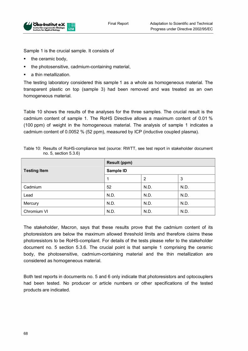
_Final Report Adaptation to Scientific and Technical
Progress under Directive 2002/95/EC
68
Sample 1 is the crucial sample. It consists of
§ the ceramic body,
§ the photosensitive, cadmium-containing material,
§ a thin metallization.
The testing laboratory considered this sample 1 as a whole as homogeneous material. Thetransparent plastic on top (sample 3) had been removed and was treated as an ownhomogeneous material.
Table 10 shows the results of the analyses for the three samples. The crucial result is thecadmium content of sample 1. The RoHS Directive allows a maximum content of 0.01 %(100 ppm) of weight in the homogeneous material. The analysis of sample 1 indicates acadmium content of 0.0052 % (52 ppm), measured by ICP (inductive coupled plasma).
Table 10: Results of RoHS-compliance test (source: RWTT, see test report in stakeholder documentno. 5, section 5.3.6)
Result (ppm)
Sample IDTesting Item
1 2 3
Cadmium 52 N.D. N.D.
Lead N.D. N.D. N.D.
Mercury N.D. N.D. N.D.
Chromium VI N.D. N.D. N.D.
The stakeholder, Macron, says that these results prove that the cadmium content of itsphotoresistors are below the maximum allowed threshold limits and therefore claims thesephotoresistors to be RoHS-compliant. For details of the tests please refer to the stakeholderdocument no. 5 section 5.3.6. The crucial point is that sample 1 comprising the ceramicbody, the photosensitive, cadmium-containing material and the thin metallization areconsidered as homogeneous material.
Both test reports in documents no. 5 and 6 only indicate that photoresistors and optocouplershad been tested. No producer or article numbers or other specifications of the testedproducts are indicated.

Adaptation to Scientific and TechnicalProgress under Directive 2002/95/EC
Final Report
69
ERA test reports from stakeholder consultation 7 and from the review process
In the 7th stakeholder consultation, Casco Silonex had submitted a test report by ERA statingthat the Macron photoresistors are not RoHS-compliant (see section 5.3.6, document no. 7).However, it was not indicated in the report, which Macron model of photoresistor had beenassessed. Macron stated that it produces both RoHS-compliant and non-RoHS-compliantphotoresistors and optocouplers, and that the photoresistor tested by ERA was not from itsRoHS-compliance models.
Another test reports was submitted during the review process (document no. 11, section5.3.6). This test report is from ERA by the order of Casco Silonex as well and negates theRoHS compliance of the assessed Macron products. In opposite to the first ERA report, ERAthis time specifies the tested Macron devices:
§ MI 1210CLA-R (type “A”)
§ MI 1210CLB-R (type “B”)
§ MI 1210CLH-R (type “C”)
ERA states that Macron claims these three photoresistors to be RoHS compliant. Thisstatement of ERA in principle is congruent with Macron’s information that the three versionsof its MI1210CL-R model is one of its three RoHS-compliant photoresistor models. The “C”-denomination of the last of the three series, the MI1210CLH-R, is not congruent withMacron’s information. According to Macron, this is the “H”-series, and there is no informationfrom Macron whether a “C”-series actually exists. In the ERA test report, the MI 1210CLH-Rmodel is sometimes addressed as “C”-type, sometimes as “H”-type (e.g. in Table 9).
Figure 12: Image of Macron photocell (source: ERA, see document 7 in references, section 5.3.6)
The above image is from the first ERA report submitted during the stakeholder consultation.It is not clear which photoresistor this image shows, as the report does not specify this. It isshown here nevertheless as it helps understanding the sampling and the results of ERA in

_Final Report Adaptation to Scientific and Technical
Progress under Directive 2002/95/EC
70
the second report. As only the second ERA report (document no. 11 in references) allows aclear attribution of the test results to clearly specified products, the following results weretaken from this second report.
ERA challenges the homogeneous material definition of the RWTT test reports. Thesample 1 in the Macron test report no. 5 can be mechanically disjointed into twohomogeneous materials:
§ the ceramic base
§ photosensitive layer containing cadmium and the metallisation (cannot be mechanicallydisjointed from cadmium layer)
ERA describes the preparation of the homogeneous material and the testing as follows(document no. 11, section 5.3.6):
“Each device was cut into two parts using a diamond saw. This separates the LEDs from thelight dependent resistors [the Macron devices obviously are optocouplers, not singlephotoresistors; the contractors]. The light dependent resistors have coatings of a transparentgel over a thin metal mask that defines the resistor path which is made of the photosensitivematerial.”
Figure 13: Light dependent resistors from Macron optocoupler type “A”, type “B” and type “C” (left toright) (source: ERA, see reference document no. 11, section 5.3.6)
“It was possible to use a surgical scalpel to scrape off the transparent gel. The metal layerwas very thin and could not be separated from the photosensitive layer and so these areremoved together with the scalpel as one material which was transferred to an adhesivestub.”
ERA says that they scraped the photosensitive layer with metal mask off the substrate frombetween the metal pins, which are visible as the two silvery circles in each type ofphotoresistor in the above and below figures. According to ERA, the pins are soldered into

Adaptation to Scientific and TechnicalProgress under Directive 2002/95/EC
Final Report
71
position and the solder contains tin but no tin was detected in the analysis sample and thisshows that it was possible to avoid the pins.
Figure 14: Light dependent resistors from Macron opto-coupler type “A”, “B” “C” (left to right) after thegel and photosensitive material coatings had been removed (source: ERA, document no.11, section 5.3.6)
“The stubs are designed for insertion into a Scanning Electron Microscope (SEM) andmaterials are analysed using energy dispersive X-ray (EDX) analysis.
This analysis technique was chosen, as it is able to analyse very small quantities of material.If many optocouplers had been available, it would be possible to scrape off sufficientphotosensitive layer for analysis by other techniques such as Inductively Coupled Plasma(ICP) Spectroscopy but ERA had only two of each type available. “
Table 11: SEM/EDX analysis of photosensitive coating from Macron optocouplers
Results (weight percent) Comments
“A“ Cadmium 60,6 %, sulphur 15,5%, selenium 5,5 % This material is cadmium sulphide/selenide
“B“ Cadmium 70 %, sulphur 18,4 %, selenium 4,1 % This material is cadmium sulphide/selenide
“H“ Cadmium 58,2 %, sulphur 15,1 % selenium 2,3 % This material is cadmium sulphide/selenide
(Source: ERA, document no. 11, section 5.3.6 )
ERA explains that the figures in the table for the cadmium-containing elements do not add upto 100% because small amounts of impurities from the gel coating (carbon and oxygen) andthe alumina substrate (aluminium and oxygen) have not been included.
According to the test results in Table 11, the cadmium content in the analyzed Macronphotoresistors would be clearly above 0.01 %. The optocouplers would thus not be RoHS-compliant. For details, refer to document no. 11 in references, section 5.3.6.

_Final Report Adaptation to Scientific and Technical
Progress under Directive 2002/95/EC
72
Additional Macron Test Report
Macron, as a reaction on the ERA test report submitted during the seventh stakeholderconsultation (document 7, section 5.3.6), insisted on the RoHS compliance of itsphotoresistors and submitted a new test report during the exemption review process(document no. 12 in references, section 5.3.6).
The report contains an explication about Macron’s technology:
“Traditional photocells usually contain a layer of CdS/CdSe which act as a photosensitivelayer. However, Macron has developed a new technology where much lesser cadmium isrequired to obtain the same function. The innovative manufacturing method from Macron is anew process that mixes cadmium into the ceramic base, which allows the ceramic base tohave photosensitive function. For this reason, Macron’s photocell can only be separate intothree homogeneous materials (transparent plastic, white ceramic and silvery metal).
Macron uses the innovative technology of photosensitive ceramic instead of using anadditional photosensitive CdS/CdSe layer. According to the definition of the EU Commission,this ceramic base cannot be “mechanically disjointed” from the white ceramic part. Therefore,the ceramic base -cadmium mixture should be counted as the same homogeneous materialwith the white ceramic part.”
Macron was asked whether the ceramic base and the white ceramic part are two differentmaterials. Macron explained, “The ceramic base and the white ceramic part refer to the sameceramic part. It must be a typo. In this sentence “According to the definition of the EUCommission, this ceramic base cannot be “mechanically disjointed” from the white ceramicpart.”, “ceramic base” should really mean “cadmium”. In our manufacturing process,cadmium was mixed into the ceramic before it cools; there is only 1 ceramic part in thephotocell unit.” (Source: Macron, received via e-mail 31 August 2007).
“White ceramic” is also used in other sections of the test report, e.g. in the following figure aswell as in the description of the samplings and the analyses in Table 8 in section 5.3.4.1.
This denomination is consistent throughout the test report no. 12 in section 5.3.6. The testinglaboratory considers the white ceramic part as homogeneous material, as the following figureunderpins.

Adaptation to Scientific and TechnicalProgress under Directive 2002/95/EC
Final Report
73
Figure 15: Physical appearance and homogeneous materials in Macron photoresistors (source: RWTTtest report, document no. 12 in references in section 5.3.6)
The report specifies the tested product as Macron’s MI 1210CLA-R (A-type), which accordingto Macron has the highest content of cadmium to achieve a high photosensitivity.
The testing laboratory, RWTT, has taken a different approach for the sampling this timecompared with the previous Macron reports described before. The following table shows thesampling procedure and the cadmium content for each of the obtained samples. Thesamples were analyzed using XRF analysis.

_Final Report Adaptation to Scientific and Technical
Progress under Directive 2002/95/EC
74
Table 12: Sampling and XRF analysis results of obtained samples
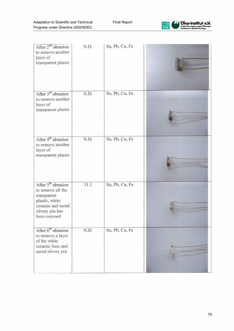
Adaptation to Scientific and TechnicalProgress under Directive 2002/95/EC
Final Report
75

_Final Report Adaptation to Scientific and Technical
Progress under Directive 2002/95/EC
76
Source: Macron test report/RWTT, document no. 12, section 5.3.6
According to these test results, only the last bit of transparent layer (material of 5th abrasion)would contain 0.0031 % (31.1 ppm) of cadmium, which is below the maximum allowed levelof 0.01 % for RoHS compliance. The photoresistor would thus be RoHS-compliant. Fordetails, refer to document no. 12 in references in section 5.3.6.
Macron was asked to explain the results. The cadmium, according to the process descriptionin the test report, is mixed into the ceramic base. The test result, however, indicates nodetectable cadmium in the ceramic base, but only in the last bit of abraded transparentplastic.

Adaptation to Scientific and TechnicalProgress under Directive 2002/95/EC
Final Report
77
Macron explained that the cadmium was detected in the 5th abrasion of the transparent layerbecause RWTT might have abraded parts of the white ceramic with the last bit of transparentlayer. There is no cadmium in the transparent layer, according to Macron, but the cadmiumconcentration should be higher nearer to the photosensitive surface of the ceramic and ittherefore was detected with the first abrasions of the white ceramic. Macron said it could notprove the higher cadmium surface at the surface, as it had no clear evidence. Macron statedthat it did not see how the sampling was done and there is no standard of how deep thesample should be abraded before each analysis. Macron itself relativised this statement in alater e-mail saying that the detected cadmium comes from the top of the ceramic abradedwith the last bit of transparent layer, and there is a gradient of cadmium content from thesurface towards the inside of the ceramic body. Macron did not explain why later it was sureof the gradient of cadmium content, while before it was just expressed as an assumption.
Macron states that the process of making the photo-sensitive ceramic is one possibleexplanation for the cadmium content of 0.003 % analysed with the last bit of transparentlayer. During the early stage of the cooling process of the photosensitive ceramic, before theceramic hardens, a small amount of cadmium added is sedimented to the bottom of thephoto-sensitive ceramic. The bottom of this photosensitive ceramic becomes thephotosensitive surface, where a layer of the transparent plastic is added. This processingmakes plausible that there could be a gradient of cadmium content with higher contents ofcadmium in the material directly under the transparent layer. This would mean, on the otherhand, that the cadmium is not really mixed INTO the liquid ceramic, as described before.Macron did not give further explanations on the processing issue.
Macron says the fact that no cadmium could be detected in the later abrasions after the 5th
one may have to do with the XRF analysis. The XRF analysis deviates within ± 50 ppm(± 0.005%), as also mentioned in the ERA report. Macron states that its photosensitiveceramic contains cadmium under the surface layer, too, but, as the inside only contains traceamounts of cadmium, it cannot be detected with the XRF analysis. In another statement,Macron says that for each of its optocouplers, a total of around 80 ppm of CdS and CdSe areadded into the ceramic liquid for mixing. Macron says that the 80 ppm of CdS/CdSe arealready related to the weight of the solid ceramic, not the liquid ceramic.
This corresponds to a cadmium content of around 0.004 % of cadmium for CdSe and around0.006 % for CdS. As both cadmium compounds are mixed, the calculatory average cadmiumcontent should be somewhere in between neglecting the gradient of cadmium content fromthe surface towards the inner ceramic.
The contractors did not go further into details of the test results, as this would be beyond thepossibilities of their mandate.

_Final Report Adaptation to Scientific and Technical
Progress under Directive 2002/95/EC
78
Homogeneous material definition and interpretations in the tests
The applicants and stakeholders have submitted tests which arrive at different, contrary andcontroversial results. While the ERA test reports by the order of Silonex shall prove that theproducts, which Macron specifies as RoHS-compliant, are not RoHS-compliant, the RWTTtest reports by the order of Macron shall prove the opposite.
A part of the discussion is what should be considered as the homogeneous material in theassessed products. As mentioned before, the contractors will not assume a position in thisdiscussion, but just show the different standpoints.
The Commission's frequently-asked-questions (FAQ) document(http://ec.europa.eu/environment/waste/weee/pdf/faq_weee.pdf) informs in section 2.3:
“2.3. Are maximum concentration values set in the RoHS Directive?
For the purposes of Article 5(1)(a) the Commission has adopted Decision 2005/618/ECwhereby a maximum concentration value of 0.1% by weight in homogeneous materials forlead, mercury, hexavalent chromium, polybrominated biphenyls (PBB) and polybrominateddiphenyl ethers (PBDE) and of 0.01% weight in homogeneous materials for cadmium shallbe allowed.
Homogeneous material means a material that cannot be mechanically disjointed intodifferent materials.
Definitions:
The term “homogeneous” means “of uniform composition throughout”. Examples of“homogeneous materials” are individual types of: plastics, ceramics, glass, metals, alloys,paper, board, resins and coatings.
The term “mechanically disjointed” means that the materials can, in principle, be separatedby mechanical actions such as: unscrewing, cutting, crushing, grinding and abrasiveprocesses.
Examples:§ A plastic cover is a “homogeneous material” if it consists of one type of plastic that is not
coated with or has attached to it or inside it any other kinds of materials. In this case, thelimit values of the Directive would apply to the plastic.
§ An electric cable that consists of metal wires surrounded by non-metallic insulationmaterials is an example of a “non-homogeneous material” because the different materialscould be separated by mechanical processes. In this case, the limit values of theDirective would apply to each of the separated materials individually.
§ A semi-conductor package contains many homogeneous materials which include: plasticmoulding material, tin-electroplating coatings on the lead frame, the lead frame alloy andgold-bonding wires.”

Adaptation to Scientific and TechnicalProgress under Directive 2002/95/EC
Final Report
79
(End of quotation from the Commission’s FAQ-document)
Both test reports refer to the above definitions in the Commission’s FAQ-document or therespective phrases in the RoHS Directive and technical guidance documents.
ERA adds that the definition of homogeneous materials is simply a definition; it is clearly notan instruction for chemical analysis. ERA explains that if one material in principal can beseparated from another then these are separate materials, even if a “clean” separation is notpossible or it is impossible to separate sufficient material for chemical analysis to be carriedout. ERA cites a document published by the RoHS Enforcement Network (see page 13 ofdocument no. 12 in section 5.3.6) as reference for this position.
ERA in its test report describes the photoresistors for which Macron claims RoHScompliance and draws conclusions:
“The photocell is made from a ceramic disc with a deposited layer containing cadmium. Thisis heated then to create the photosensitivity. Macron state that after heating, the surfacelayer cannot be “mechanically disjointed” from the ceramic substrate. This is a crucial pointand one that needs to be tested. Note that the definition of mechanical disjointing is that thematerials can, in principal, be separated by mechanical actions indicates and so implies thatseparation need not be perfect.“ (source: document no. 7, section 5.3.6)
ERA made several abrasions of the ceramic base after removal of the transparent plasticlayer. The materials obtained via these abrasions are considered as homogeneous material.The cadmium content in these abraded materials is clearly above the maximum allowedthreshold level of 0.01 % of cadmium. ERA concludes that the tested Macron photoresistorsare not RoHS-compliant.
RWTT has tested the Macron photoresistor and describes the product as well as how it ismanufactured and draws conclusions concerning the homogeneous material:
“In the traditional photocell manufacturing method, a thin layer of CdS/CdSe is sprayed ontoa ceramic base. [...] However, Macron has developed a new technology where much lessercadmium is required to obtain the same function. The innovative manufacturing method fromMacron is a new process that mixes cadmium into the ceramic base, which allows theceramic base to have photosensitive function. For this reason, Macron’s photocell can onlybe separate into three homogeneous materials (transparent plastic, white ceramic and silverymetal). Macron uses the innovative technology of photosensitive ceramic instead of using anadditional photosensitive CdS/CdSe layer. According to the definition of the EU Commission,this ceramic base cannot be “mechanically disjointed” from the white ceramic part.
Therefore, the ceramic base cadmium mixture should be counted as the same homogeneousmaterial with the white ceramic part.” (Source: document no. 12, section 5.3.6).
RWTT made several abrasions of the ceramic body including the silvery pins. Each of thedifferent abraded materials was tested for its cadmium content.

_Final Report Adaptation to Scientific and Technical
Progress under Directive 2002/95/EC
80
None of these materials exceeded the 0.01 % of cadmium content. RWTT concludes that theassessed Macron photoresistor is RoHS-compliant.
ERA says that the abrasion of material was conducted in between the silvery pins. Thetested material thus did not include any constituents of these silvery pins. RWTT hadabraded the tested material after removal of the transparent plastic layer from the surfaceincluding the silvery pins. It is not clear whether and how far this has an influence on the testresults.
Furthermore, Macron says that its A-type photoresistor has the highest contents of cadmiumand therefore had this type tested. ERA, however, measured the highest cadmium contentsin the B-type photoresistor. According to the ERA results, its cadmium content is around10 % higher than in the A-type.
The RWTT and the ERA tests arrive at contrary, conflicting results. They state the RoHS-compliance and non-RoHS-compliance of the tested Macron photoresistors respectively. Thedifferences cannot only be explained with different homogeneous material definitions. Thedescription of the tested Macron photoresistor from ERA and from RWTT already differconsiderably, as the above quotations from the test documents show, although the articlenumbers coincide. It could have been expected that the ERA test and the second RWTT test(document no. 12 in section 5.3.6) arrive at similar results, as in both cases the sampling isdone by abrasion from the ceramic body. The inclusion of the silvery pins in the RWTT testmight in parts explain the differences. Several reasons might be possible for the deviations,although, considering the huge differences between the results ranging from “not detectable”up to around 61 % of cadmium content, this might be a difficult task. The evaluation of thetest procedures and the deeper investigation into the differences between the results is,however, beyond the contractors’ mandate.
The opposing parties could agree on a test procedure and a testing lab and then have thetests conducted again. In case an agreement or other solutions are not possible, both partiesmay file a lawsuit at the European Court of Justice.