ad8452 (rev. 0) - analog devices sheet ad8452 rev. 0 document feedback information furnished by...
TRANSCRIPT

Precision Integrated Analog Front End, Controller, and PWM for Battery Test and Formation Systems
Data Sheet AD8452
Rev. 0 Document FeedbackInformation furnished by Analog Devices is believed to be accurate and reliable. However, no responsibility is assumed by Analog Devices for its use, nor for any infringements of patents or other rights of third parties that may result from its use. Specifications subject to change without notice. No license is granted by implication or otherwise under any patent or patent rights of Analog Devices. Trademarks and registered trademarks are the property of their respective owners.
One Technology Way, P.O. Box 9106, Norwood, MA 02062-9106, U.S.A.Tel: 781.329.4700 ©2017 Analog Devices, Inc. All rights reserved.Technical Support www.analog.com
FEATURES CC and CV battery test and formation modes with
transparent and automatic switchover, for systems of 20 Ah or less
Precise measurement of voltage and current Independent feedback control blocks Highly accurate, factory trimmed instrumentation and
differential amplifiers In-amp for current sense gain: 66 V/V Difference amplifier for voltage sense gain: 0.4 V/V
Stable over temperature: offset voltage drift <0.6 μV/°C (maximum)
Gain drift: <3 ppm/°C (maximum) Current sense CMRR: 120 dB minimum Popular SMPS control for charge/discharge High PWM linearity with internal ramp voltage 50 kHz to 300 kHz user controlled switching frequency Synchronization output or input with adjustable phase shift Programmable soft start
APPLICATIONS Battery formation and testing High efficiency battery test systems with recycle capability Battery conditioning (charging and discharging) systems
GENERAL DESCRIPTION The AD8452 combines a precision analog front-end controller and switch mode power supply (SMPS), pulse-width modulator (PWM) driver into a single silicon platform for high volume battery testing and formation manufacturing. A precision instrumentation amplifier (in-amp) measures the battery charge/ discharge current to better than ±0.1% accuracy, while an equally accurate difference amplifier measures the battery voltage. Internal laser trimmed resistor networks establish the in-amp and difference amplifier gains (66 V/V and 0.4 V/V, respectively), and stabilize the AD8452 performance across the rated operating temperature range.
Desired battery cycling current and voltage levels are established by applying precise control voltages to the ISET and VSET inputs. Actual charge and discharge current levels are sensed (usually by a high power, highly accurate shunt resistor) whose value is carefully selected according to system parameters. Switching between constant current (CC) and constant voltage (CV) loop integration is instantaneous, automatic, and completely transparent to the observer. A logic high at the MODE input selects the charge or discharge mode (high for charge, low for discharge).
The AD8452 simplifies designs by providing excellent performance, functionality, and overall reliability in a space saving 48-lead, 7 mm × 7 mm × 1.4 mm LQFP package rated for operation at temperatures from −40°C to +85°C.
FUNCTIONAL BLOCK DIAGRAM
IBATIN-AMP
VBATDIFFAMP
ISM
EA
ISET
BVM
EA
FAULTISVN
ISVP
BVN
BVP
VIN
T
×1
MO
DE
AD8452
IVE0
/IVE1
BVREFH/BVREFL
ISREFH/ISREFL
VREF
VREF0.4× 66×
CV FILTERAMPLIFIER
SYSTEM CONTROL
VSET
VVE0
/VVE
1
SYNC
VIN
DT
DH
DL
SCFG
DMAX
FREQ
DGND
CLNCLPEN
+DCBUS
VCL
VCL
ISVBV
ISV
BV
SS
CLVTPWM
LOOPCOMP (×4)
MODESELECT
CC FILTERAMPLIFIER
MOSFETDRIVER
1618
7-00
1
Figure 1.

AD8452 Data Sheet
Rev. 0 | Page 2 of 34
TABLE OF CONTENTS Features .............................................................................................. 1
Applications ....................................................................................... 1
General Description ......................................................................... 1
Functional Block Diagram .............................................................. 1
Revision History ............................................................................... 2
Specifications ..................................................................................... 3
Analog Front-End and Controller Specifications .................... 3
Pulse-Width Modulator Specifications ..................................... 5
Digital Interface Specifications ................................................... 6
Power Supply ................................................................................. 7
Temperature Range Specifications ............................................. 7
Absolute Maximum Ratings ............................................................ 8
Thermal Resistance ...................................................................... 8
ESD Caution .................................................................................. 8
Pin Configuration and Function Descriptions ............................. 9
Typical Performance Characteristics ........................................... 11
In-Amp Characteristics ............................................................. 11
Difference Amplifier Characteristics ....................................... 12
CC and CV Loop Filter Amplifiers and VSET Buffer (except where Noted) ............................................................................... 13
Reference Characteristics .......................................................... 15
Pulse-Width Modulator ............................................................. 16
Theory of Operation ...................................................................... 18
Introduction ................................................................................ 18
Instrumentation Amplifier (In-Amp) ..................................... 19
Difference Amplifier .................................................................. 20
CC and CV Loop Filter Amplifiers .......................................... 20
Charge and Discharge Control ................................................. 23
Input and Output Supply Pins .................................................. 23
Shutdown ..................................................................................... 24
Undervoltage Lockout (UVLO) ............................................... 24
Soft Start ...................................................................................... 24
PWM Drive Signals .................................................................... 25
Peak Current Protection and Diode Emulation (Synchronous) ............................................................................. 25
Frequency and Phase Control .................................................. 26
Maximum Duty Cycle ............................................................... 26
Fault Input ................................................................................... 27
Thermal Shutdown (TSD) ........................................................ 27
Applications Information .............................................................. 28
Analog Controller ...................................................................... 28
Functional Description .............................................................. 28
Power Supply Connections ....................................................... 29
Current Sense In-Amp Connections ....................................... 29
Voltage Sense Differential Amplifier Connections ................ 29
Battery Current and Voltage Control Inputs (ISET and VSET) ........................................................................ 29
Loop Filter Amplifiers ............................................................... 30
Selecting Charge or Discharge Options .................................. 30
Select RCL and RCLVT for the Peak Current Limit .................. 30
Setting the Operating Frequency and Programming the Synchonization Pin .................................................................... 31
Programming the Maximum Duty Cycle ............................... 32
Selecting CSS ................................................................................ 33
Additional Information ............................................................. 33
Outline Dimensions ....................................................................... 34
Ordering Guide .......................................................................... 34
REVISION HISTORY 10/2017—Revision 0: Initial Version

Data Sheet AD8452
Rev. 0 | Page 3 of 34
SPECIFICATIONS AVCC = 15 V, AVEE = −15 V, VIN = 24 V, and TA = 25°C, unless otherwise noted.
ANALOG FRONT-END AND CONTROLLER SPECIFICATIONS
Table 1. Parameter Test Conditions/Comments Min Typ Max Unit CURRENT SENSE INSTRUMENTATION
AMPLIFIER
Gain 66 V/V Gain Error VISMEA = ±10 V ±0.1 % Gain Drift TA = TMIN to TMAX 3 ppm/°C
Offset Voltage Referred to Input (RTI) ISREFH pin and ISREFL pin grounded −100 +100 µV Offset Voltage Drift TA = TMIN to TMAX −0.6 −0.1 +0.6 µV/°C
Input Bias Current 15 30 nA Input Common-Mode Voltage Range VISVP − VISVN = 0 V AVEE + 2.3 AVCC − 2.4 V Differential Input Impedance 150 GΩ Common-Mode Input Impedance 150 GΩ Output Voltage Swing RL = 10 kΩ AVEE + 1.5 AVCC − 1.2 V Reference Input Voltage Range ISREFH pin and ISREFL pin tied together AVEE + 1.5 AVCC − 1.5 V Reference Bias Current VISVP = VISVN = 0 V 5 µA Output Voltage Level Shift ISREFL pin grounded
Maximum ISREFH pin connected to VREF pin 11 12.5 14 mV Scale Factor VISMEA/VISREFH 4.4 5 5.6 mV/V
Short-Circuit Current 40 mA Common-Mode Rejection Ratio (CMRR) ΔVCM = 20 V 120 dB
Temperature Coefficient TA = TMIN to TMAX 0.01 µV/V/°C Power Supply Rejection Ratio (PSRR) ΔVS = 10 V 122 140 dB Small Signal −3 dB Bandwidth 675 kHz Slew Rate ΔVISMEA = 10 V 5 V/µs
VOLTAGE SENSE DIFFERENCE AMPLIFIER Gain 0.4 V/V
Gain Error VIN = ±10 V ±0.1 % Gain Drift TA = TMIN to TMAX 3 ppm/°C
Offset Voltage Referred to Output (RTO) BVREFH pin and BVREFL pin grounded −250 +250 µV Offset Voltage Drift TA = TMIN to TMAX −2 −0.1 +2 µV/°C
Differential Input Voltage Range VBVN = 0 V, VBVREFL = 0 V −17 +17 V Input Common-Mode Voltage Range VBVMEA = 0 V −40 +40 Differential Input Impedance 400 kΩ Input Common-Mode Impedance 140 kΩ Output Voltage Swing RL = 10 kΩ AVEE + 1.5 AVCC − 1.2 V Reference Input Voltage Range BVREFH pin and BVREFL pin connected AVEE + 1.5 AVCC − 1.5 V Output Voltage Level Shift BVREFL pin grounded
Maximum BVREFH pin connected to VREF pin 11.0 12.5 14.0 mV Scale Factor VBVMEA/VBVREFH 4.4 5 5.6 mV/V
Short-Circuit Current 40 mA CMRR ΔVCM = 10 V, RTO 90 dB
Temperature Coefficient TA = TMIN to TMAX 0.05 µV/V/°C PSRR ΔVS = 10 V, RTO 114 123 dB Small Signal −3 dB Bandwidth 3.0 MHz Slew Rate ΔVBVMEA = 10 V 0.9 V/µs

AD8452 Data Sheet
Rev. 0 | Page 4 of 34
Parameter Test Conditions/Comments Min Typ Max Unit CC AND CV LOOP FILTER AMPLIFIERS
Offset Voltage 150 µV Offset Voltage Drift TA = TMIN to TMAX −1 +0.02 1 µV/°C
Input Bias Current −5 +5 nA Input Common-Mode Voltage Range AVEE + 1.5 AVCC − 1.8 V Output Voltage Swing VVINT voltage range AVEE + 1.5 5 V Source Short-Circuit Current 1 mA Sink Short-Circuit Current 40 mA PSRR ΔVS = 10 V 113 122 dB Small Signal Gain Bandwidth Product 3 MHz Slew Rate ΔVVINT = 10 V 1 V/μs CC to CV Transition Time 1.8 µs
VSET VOLTAGE BUFFER Nominal Gain 1 V/V Offset Voltage 150 µV
Offset Voltage Drift TA = TMIN to TMAX −1 +0.06 +1 µV/°C Input Bias Current −5 +5 nA Input/Output Voltage Range AVEE + 1.5 AVCC − 1.8 V Short-Circuit Current 40 mA PSRR ΔVS = 10 V 113 122 dB Small Signal −3 dB Bandwidth 4 MHz Slew Rate ΔVVSETBF = 10 V 1 V/μs
VOLTAGE REFERENCE Nominal Output Voltage With respect to AGND 2.5 V Output Voltage Error ±1 % Temperature Drift TA = TMIN to TMAX 16 ppm/°C Line Regulation ΔVS = 10 V 10 ppm/V Load Regulation ΔIVREF = 1 mA (source only) 300 ppm/mA Source Short-Circuit Current 15 mA

Data Sheet AD8452
Rev. 0 | Page 5 of 34
PULSE-WIDTH MODULATOR SPECIFICATIONS
Table 2. Parameter Test Conditions/Comments Min Typ Max Unit SOFT START (SS)
SS Pin Current VSS = 0 V 4 5 6 µA SS Threshold Rising Switching enable threshold 0.52 0.65 V SS Threshold Falling Switching disable threshold 0.4 0.5 V End of Soft Start Asynchronous to synchronous threshold 4.4 4.5 4.6 V
PWM CONTROL Frequency
Frequency Range RFREQ = 33.2 kΩ to 200 kΩ 50 300 kHz Oscillator Frequency RFREQ = 100 kΩ 90 100 110 kHz FREQ Pin Voltage RFREQ = 100 kΩ 1.1 1.255 1.4 V
SYNC Output (Internal Frequency Control)
VSCFG ≥ 4.53 V or SCFG pin floating
Internal SYNC Range For SYNC output 50 300 kHz SYNC Output Clock Duty Cycle VSCFG = VVREG, RFREQ = 100 kΩ 40 50 60 % SYNC Sink Pull Down Resistance VSCFG = 5 V, ISYNC = 10 mA 10 20 Ω
SYNC Input (External Frequency Control) VSCFG < 4.25 V External SYNC Range For SYNC input clock 50 300 kHz SYNC Internal Pull-Down Resistor 0.5 1 1.5 MΩ Maximum SYNC Pin Voltage For external sync operation 5 V SYNC Threshold Rising 1.2 1.5 V SYNC Threshold Falling 0.7 1.05 V
SCFG SCFG High Threshold
Rising SYNC set to input 4.53 4.7 V Falling SYNC set to output 4.25 4.47 V
SCFG Low Threshold Rising Programmable phase shift above threshold 0.55 0.65 V Falling No phase shift 0.4 0.5 V
SCFG Pin Current RFREQ = 100 kΩ, VSCFG = DGND 10 11 12 µA DMAX
Maximum Internal Duty Cycle VDMAX, VSS, and VSCFG = 5 V 97 % DMAX Setting Current VDMAX = 0 V, RFREQ = 100 kΩ 10 11 12 µA DMAX and SCFG Current Matching1 10 %
DT DT Pin Current RFREQ = 100 kΩ, VDT = DGND 20 24 µA Maximum DT Programming Voltage See Figure 28 3.5 V
CURRENT LIMIT (CL) CLVT
CLVT Pin Current Minimum CLVT pin voltage = 50 mV 16 21 27 µA CLP, CLN
Common-Mode Range VCLP = VCLN 0 8 V Input Resistance 24 30 36 kΩ
Current Limit Threshold Offset VCLP = VCLN, RCLVT = 2.49 kΩ 50 mV CLFLG Open-drain, active low output
Max CLFLG Voltage Open-drain output 5.5 V
CFLG Pull-Down Resistance 8 Ω
Current Limit RFREQ = 100 kΩ, 16 consecutive clock pulses Overload Time 160 μs Cool Down Time 160 μs

AD8452 Data Sheet
Rev. 0 | Page 6 of 34
Parameter Test Conditions/Comments Min Typ Max Unit ZERO CROSSING DETECTION (ZCD)
ZCD Threshold Offset (VCLP + VCLN)/2, for common-mode voltage (CMV) = 0 V to 8 V
0 mV
VREG Low Dropout (LDO) Regulator Output
Voltage VIN = 6 V to 60 V, no external load 4.9 5 5.1 V
Load Regulation VIN = 6 V, IOUT = 0 mA to 5 mA 4.9 5 5.1 V PWM DRIVE LOGIC SIGNALS (DH/DL)
DL Drive Voltage No load VREG V DH Drive Voltage No load VREG V DL and DH Sink Resistance IDL = 10 mA 1.4 2.6 Ω DL and DH Source Resistance IDL = 10 mA 1.4 2.6 Ω DL and DH Pull-Down Resistor 0.5 1 1.5 MΩ
THERMAL SHUTDOWN (TSD) TSD Threshold
Rising 150 °C Falling 125 °C
1 The DMAX and SCFG current matching specification is calculated by taking the absolute value of the difference between the measured ISCFG and IDMAX currents, dividing
them by the 11 µA typical value, and multiplying this result by 100. DMAX and SCFG current matching (%) = (ISCFG – IDMAX/11 µA) × 100
DIGITAL INTERFACE SPECIFICATIONS
Table 3. Parameter Test Conditions/Comments Min Typ Max Unit DIGITAL INTERFACE, MODE INPUT MODE pin
MODE Threshold Rising 1.2 1.4 V MODE Threshold Falling 0.7 1.0 V MODE Switching Time 400 ns
PRECISION ENABLE LOGIC (EN) Maximum EN Pin Voltage 60 V EN Threshold Rising 1.26 1.4 V EN Threshold Falling 1.1 1.2 V EN Pin Current VEN = 5 V, internal pull-down 0.25 2 µA
FAULT Active low input
Maximum FAULT Pin Voltage 60 V
FAULT Threshold Rising 1.2 1.5 V
FAULT Threshold Falling 0.7 1.0 V
FAULT Pin Current VFAULT = 5 V, internal 8.5 MΩ pull-down resistor
0.5 2 µA
Data Sheet AD8452
Rev. 0 | Page 7 of 34
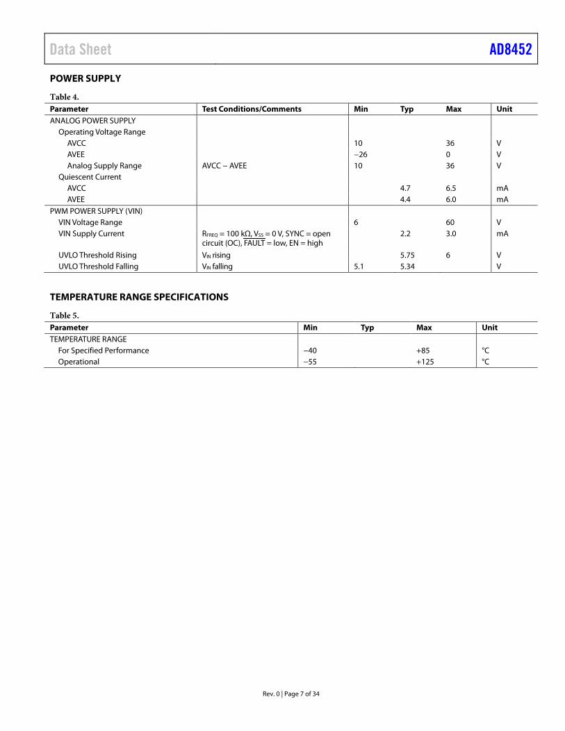
POWER SUPPLY
Table 4. Parameter Test Conditions/Comments Min Typ Max Unit ANALOG POWER SUPPLY
Operating Voltage Range AVCC 10 36 V AVEE −26 0 V Analog Supply Range AVCC − AVEE 10 36 V
Quiescent Current AVCC 4.7 6.5 mA AVEE 4.4 6.0 mA
PWM POWER SUPPLY (VIN) VIN Voltage Range 6 60 V VIN Supply Current RFREQ = 100 kΩ, VSS = 0 V, SYNC = open
circuit (OC), FAULT = low, EN = high 2.2 3.0 mA
UVLO Threshold Rising VIN rising 5.75 6 V UVLO Threshold Falling VIN falling 5.1 5.34 V
TEMPERATURE RANGE SPECIFICATIONS
Table 5. Parameter Min Typ Max Unit TEMPERATURE RANGE
For Specified Performance −40 +85 °C Operational −55 +125 °C

AD8452 Data Sheet
Rev. 0 | Page 8 of 34
ABSOLUTE MAXIMUM RATINGS Table 6. Parameter Rating Analog Supply Voltage (AVCC − AVEE) 36 V PWM Supply Voltage (VIN – DGND) −0.3 V to +61 V Internal Regulator Voltage (VREG − DGND) 5.5 V Voltage
Input Pins (ISVP, ISVN, BVP, and BVN) AVEE + 40 V Analog Controller and Front-End Pins
(ISREFH, ISREFL, BVREFL, BVREFH, VREF, VSET, VVP0, BVMEA, VVE0, VVE1, VINT, IVE0, IVE1, ISMEA, ISET)
AVCC − 40 V
PWM Pins SYNC, MODE −0.3 V to +5.5 V DH, DL, SS, DMAX, SCFG, DT, FREQ, CLVT −0.3 V to
VREG + 0.3 V Current Limit Sense Pins (CLP, CLN) −0.3 V to +61 V FAULT Pin and EN Pin −0.3 V to +61 V
Maximum Digital Supply Voltage Positive Analog Supply (VREG − AVCC) 0.3 V Negative Analog Supply (VREG − AVEE) −0.3 V
Maximum Digital Ground Positive Analog Supply (DGND − AVCC) 0.3 V Negative Analog Supply (DGND − AVEE) −0.3 V
Maximum Analog Ground Positive Analog Supply (AGND − AVCC) 0.3 V Negative Analog Supply (AGND − AVEE) −0.3 V
Analog Ground with Respect to the Digital Ground (AGND − DGND)
Maximum 0.3 V Minimum −0.3 V
Storage Temperature Range −65°C to +150°C
Stresses at or above those listed under Absolute Maximum Ratings may cause permanent damage to the product. This is a stress rating only; functional operation of the product at these or any other conditions above those indicated in the operational section of this specification is not implied. Operation beyond the maximum operating conditions for extended periods may affect product reliability.
THERMAL RESISTANCE Thermal performance is directly linked to printed circuit board (PCB) design and operating environment. Careful attention to PCB thermal design is required.
Table 7. Thermal Resistance Package Type θJA
2 Unit ST-481 81 °C/W 1 Dissipation ≤ 0.3, TA = 25°C. 2 θJA is the natural convection junction to ambient thermal resistance
measured in a one cubic foot sealed enclosure.
ESD CAUTION
Data Sheet AD8452
Rev. 0 | Page 9 of 34
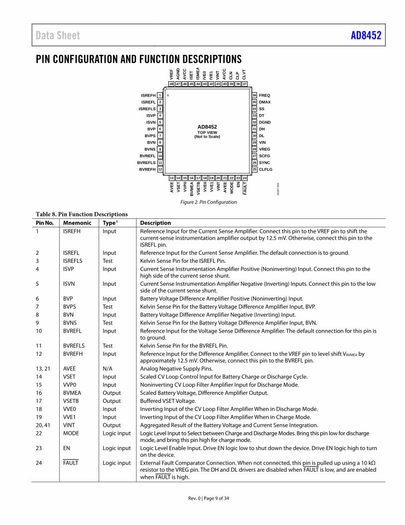
PIN CONFIGURATION AND FUNCTION DESCRIPTIONS
48 47 46 45 44 43 42 41 40 39 38 37
35
34
33
30
31
32
36
VREF
29
28
27
25
26
2
3
4
7
6
5
1
8
9
10
12
11
ISREFH
13
FREQ
14 15 16 17 18 19 20 21 22 23 24
AD8452TOP VIEW
(Not to Scale)
AVE
EA
GN
DA
VCC
ISET
ISM
EAIV
E0IV
E1VI
NT
AVC
CC
LNC
LPC
LVT
DMAXSSDTDGNDDHDLVINVREGSCFGSYNCCLFLG
ISREFLISREFLS
ISVPISVNBVP
BVPSBVN
BVNSBVREFL
BVREFLSBVREFH
VSET
VVP0
BVM
EAVS
ETB
VVE0
VVE1
VIN
TA
VEE
MO
DE
ENFA
ULT
1618
7-00
2
Figure 2. Pin Configuration
Table 8. Pin Function Descriptions Pin No. Mnemonic Type1 Description 1 ISREFH Input Reference Input for the Current Sense Amplifier. Connect this pin to the VREF pin to shift the
current-sense instrumentation amplifier output by 12.5 mV. Otherwise, connect this pin to the ISREFL pin.
2 ISREFL Input Reference Input for the Current Sense Amplifier. The default connection is to ground. 3 ISREFLS Test Kelvin Sense Pin for the ISREFL Pin. 4 ISVP Input Current Sense Instrumentation Amplifier Positive (Noninverting) Input. Connect this pin to the
high side of the current sense shunt. 5 ISVN Input Current Sense Instrumentation Amplifier Negative (Inverting) Inputs. Connect this pin to the low
side of the current sense shunt. 6 BVP Input Battery Voltage Difference Amplifier Positive (Noninverting) Input. 7 BVPS Test Kelvin Sense Pin for the Battery Voltage Difference Amplifier Input, BVP. 8 BVN Input Battery Voltage Difference Amplifier Negative (Inverting) Input. 9 BVNS Test Kelvin Sense Pin for the Battery Voltage Difference Amplifier Input, BVN. 10 BVREFL Input Reference Input for the Voltage Sense Difference Amplifier. The default connection for this pin is
to ground. 11 BVREFLS Test Kelvin Sense Pin for the BVREFL Pin. 12 BVREFH Input Reference Input for the Difference Amplifier. Connect to the VREF pin to level shift VBVMEA by
approximately 12.5 mV. Otherwise, connect this pin to the BVREFL pin. 13, 21 AVEE N/A Analog Negative Supply Pins. 14 VSET Input Scaled CV Loop Control Input for Battery Charge or Discharge Cycle. 15 VVP0 Input Noninverting CV Loop Filter Amplifier Input for Discharge Mode. 16 BVMEA Output Scaled Battery Voltage, Difference Amplifier Output. 17 VSETB Output Buffered VSET Voltage. 18 VVE0 Input Inverting Input of the CV Loop Filter Amplifier When in Discharge Mode. 19 VVE1 Input Inverting Input of the CV Loop Filter Amplifier When in Charge Mode. 20, 41 VINT Output Aggregated Result of the Battery Voltage and Current Sense Integration. 22 MODE Logic input Logic Level Input to Select between Charge and Discharge Modes. Bring this pin low for discharge
mode, and bring this pin high for charge mode. 23 EN Logic input Logic Level Enable Input. Drive EN logic low to shut down the device. Drive EN logic high to turn
on the device. 24 FAULT Logic input External Fault Comparator Connection. When not connected, this pin is pulled up using a 10 kΩ
resistor to the VREG pin. The DH and DL drivers are disabled when FAULT is low, and are enabled when FAULT is high.

AD8452 Data Sheet
Rev. 0 | Page 10 of 34
Pin No. Mnemonic Type1 Description 25 CLFLG Output Current-Limit Flag. CLFLG goes low and stays low when the AD8452 is in current limit mode.
Connect a 10 kΩ (minimum) resistor to the VREG pin. 26 SYNC Input/
output C lock Synchronization Pin. Synchronizes the clock (switching frequency) when multiple channels are phase interleaved. Connect a 10 kΩ (minimum) resistor to the VREG pin.
27 SCFG Input/ output
Synchronization Configuration Pin. See Table 10.
28 VREG Output Internal LDO 5 V Regulator Output and Internal Bias Supply. Connect a bypass capacitor of 1 µF or greater from this pin to ground.
29 VIN Input Supply Voltage to the PWM Section. VIN is typically the same as the output switch supply voltage. 30 DL Output Logic Drive Output for the External Low-Side Metal-Oxide Semiconductor Field-Effect Transistor
(MOSFET) Driver. 31 DH Output Logic Drive Output for the External High-Side MOSFET Driver. 32 DGND N/A Digital and PWM Ground. 33 DT Output Dead Time Programming Pin. Connect an external resistor between this pin and ground to set the
dead time. Do not leave this pin floating. 34 SS Output Soft Start Control Pin. A capacitor connected from the SS pin to ground sets the soft start ramp
time. See the Selecting CSS section. 35 DMAX Input Maximum Duty Cycle Input. Connect an external resistor to ground to set the maximum duty
cycle. If the 97% internal maximum duty cycle is sufficient for the application, tie this pin to VREG. If DMAX is left floating, this pin is internally pulled up to VREG.
36 FREQ N/A Frequency Set Pin. Connect an external resistor between this pin and ground to set the frequency between 50 kHz and 300 kHz. When the AD8452 is synchronized to an external clock (slave mode), set the slave frequency to 90% of the master frequency by multiplying the master RFREQ value by 1.11.
37 CLVT Input Current-Limit Voltage Threshold. With user selected resistor value, CLVT establishes a threshold voltage for the current limit comparator. See the Select RCL and RCLVT for the Peak Current Limit section.
38 CLP Input Current-Limit/Diode Emulation Amplifier Positive Sense Pin. 39 CLN Input Current-Limit/Diode Emulation Amplifier Negative Sense Pin. 40, 46 AVCC N/A Analog Positive Supply Pins. 42 IVE1 Input Inverting Input of the CC Loop Filter Amplifier When in Charge Mode. 43 IVE0 Input Inverting Input of the CC Loop Filter Amplifier When in Discharge Mode. 44 ISMEA Output Current Sense Instrumentation Amplifier Output. 45 ISET Input Scaled CC Voltage Loop Control Input for Battery Charge or Discharge Cycles. ISET is typically the
same for charge and discharge cycle. 47 AGND N/A Analog Ground. 48 VREF Output 2.5 V Reference. Bypass this pin with a high quality 10 nF NP0 ceramic capacitor in series with a
10 Ω (maximum) resistor.
1 N/A means not applicable.

Data Sheet AD8452
Rev. 0 | Page 11 of 34
TYPICAL PERFORMANCE CHARACTERISTICS AVCC = 15 V, AVEE = −15 V, VIN = 24 V, TA = 25°C, and RL = ∞, unless otherwise noted.
IN-AMP CHARACTERISTICS
GA
IN E
RR
OR
(p
pm
)
TEMPERATURE (°C)
30 40 50 60 70 80 900 20−10 10−20−30−40–100
0
–20
–40
–60
–80
20
40
60
1618
7-00
3
Figure 3. Gain Error vs. Temperature
INP
UT
BIA
S C
UR
RE
NT
(n
A)
INPUT COMMON-MODE VOLTAGE (V)
0 5−10 10 15−5−15
17.0
16.5
16.0
15.5
15.0
14.5
14.0
1618
7-00
4
Figure 4. Input Bias Current vs. Input Common-Mode Voltage
INP
UT
BIA
SC
UR
RE
NT
(nA
)
TEMPERATURE (°C)
30 40 50 60 70 80 900 20–10 10–20–30–40
1618
7-00
5
16
15
14
13
12
17
18
19ISVPISVN
Figure 5. Input Bias Current vs. Temperature
–60
–14010 100k
CM
RR
(d
B)
FREQUENCY (Hz)
–90
–110
–80
–100
–120
–70
–130
1k100 10k
1618
7-00
6
Figure 6. CMRR vs. Frequency
–50
–16010 100 1k 10k 100k
PS
RR
(d
B)
FREQUENCY (Hz)
–90
–110
–80
–100
–120
–70
–60
–130
–150
–140
+PSRR–PSRR
1618
7-00
7
Figure 7. PSRR vs. Frequency
40
30
20
10
0100 1k 10k 100k 1M 10M
GA
IN (
dB
)
FREQUENCY (Hz) 1618
7-00
8
Figure 8. Gain vs. Frequency

AD8452 Data Sheet
Rev. 0 | Page 12 of 34
DIFFERENCE AMPLIFIER CHARACTERISTICS
GA
IN E
RR
OR
(ppm
)
TEMPERATURE (°C)
30 40 50 60 70 80 900 20–10 10–20–30–40
1618
7-00
9–260
–180
–200
–220
–240
–160
–120
–140
ISVPISVN
Figure 9. Gain Error vs. Temperature
–50
–13010 100 1k 10k 100k
CM
RR
(dB
)
FREQUENCY (Hz)
–90
–110
–80
–100
–120
–70
–60
1618
7-01
0
Figure 10. CMRR vs. Frequency
–10
–140
PSR
R (d
B)
10 100 1k 10k 100kFREQUENCY (Hz)
90
–110
–80
–100
–120
–70
–50
–60
–130
–30
–40
–20 +PSRR–PSRR
1618
7-01
1
Figure 11. PSRR vs. Frequency
0
–10
–20
–30
–40100 1k 10k 100k 1M 10M
GA
IN (d
B)
FREQUENCY (Hz) 1618
7-01
2
Figure 12. Gain vs. Frequency

Data Sheet AD8452
Rev. 0 | Page 13 of 34
CC AND CV LOOP FILTER AMPLIFIERS AND VSET BUFFER (EXCEPT WHERE NOTED)
INPU
T O
FFSE
T VO
LTA
GE
(µV)
INPUT COMMON-MODE VOLTAGE (V)
0 5–10 10–5–15 15
150
100
50
0
–50
–100
–150
1618
7-01
3
Figure 13. Input Offset Voltage vs. Input Common-Mode Voltage
INPU
T B
IAS
CU
RR
ENT
(nA
)
TEMPERATURE (°C)
30 40 50 60 70 80 900 20–10 10–20–30–40
1618
7-01
4
0.15
0.10
0.05
0
–0.05
0.20
0.25
0.30
Figure 14. Input Bias Current vs. Temperature
INPU
T B
IAS
CU
RR
ENT
(pA
)
INPUT COMMON-MODE VOLTAGE (V)0 5–10 10–5–15 15
400
200
0
–200
–400
–600
–800
–1000
1618
7-01
5
Figure 15. Input Bias Current vs. Input Common-Mode Voltage
–40 –30 –20 –10 0 10 20 30 40 50 60 70 80 90TEMPERATURE (°C)
1618
7-01
6
1.6
1.7
OU
TPU
T SO
UR
CE
CU
RR
ENT
(mA
)1.5
1.4
1.3
1.2
1.1
1.0
Figure 16. Output Source Current vs. Temperature

AD8452 Data Sheet
Rev. 0 | Page 14 of 34
–20
–30
–40
–50
–60
–80
–70
–90
–100
–110
–120
–130
–140
–150
PSR
R (d
B)
10 100 1k 10k 100kFREQUENCY (Hz)
+PSRR–PSRR
1618
7-01
7
Figure 17. PSRR vs. Frequency
10M1M
120
–40
–20
20
0
60
100
40
80
10 100 1k 10k 100k
OPE
N L
OO
P G
AIN
(dB
)
FREQUENCY (Hz)
–45.0
–67.5
–90.0
–112.5
–135.0
–157.5
–180.0
–202.5
–225.0
PHA
SE (D
egre
es)
PHASE
GAIN
1618
7-01
8
Figure 18. Open-Loop Gain and Phase vs. Frequency for CC and CV Loop
Amplifiers
1.5
1.0
0.5
0
–0.5
–1.0
–1.50 25 50
OU
TPU
T VO
LTA
GE
(V)
TIME (µs)2010 155 3530 40 45
ISET (V)VINT (V)
1618
7-01
9
Figure 19. CC to CV Transition

Data Sheet AD8452
Rev. 0 | Page 15 of 34
REFERENCE CHARACTERISTICS 2.498
2.500
2.496
2.494
2.492
2.4900 2 3 5 7 861 4 9 10
OU
TPU
T VO
LTA
GE
(V)
OUTPUT CURRENT—SOURCING (mA)
T = +85°CT = +25°CT = –40°C
1618
7-02
0
Figure 20. Sourcing Regulation for Three Values of Temperature
300
250
200
150
100–55 –15 5 45 8565–35 25 105 125
SOU
RC
E LO
AD
REG
ULA
TIO
N (p
pm/m
A)
TEMPERATURE (°C) 1618
7-02
1
Figure 21. Source Load Regulation vs. Temperature
AD8452 Data Sheet
Rev. 0 | Page 16 of 34
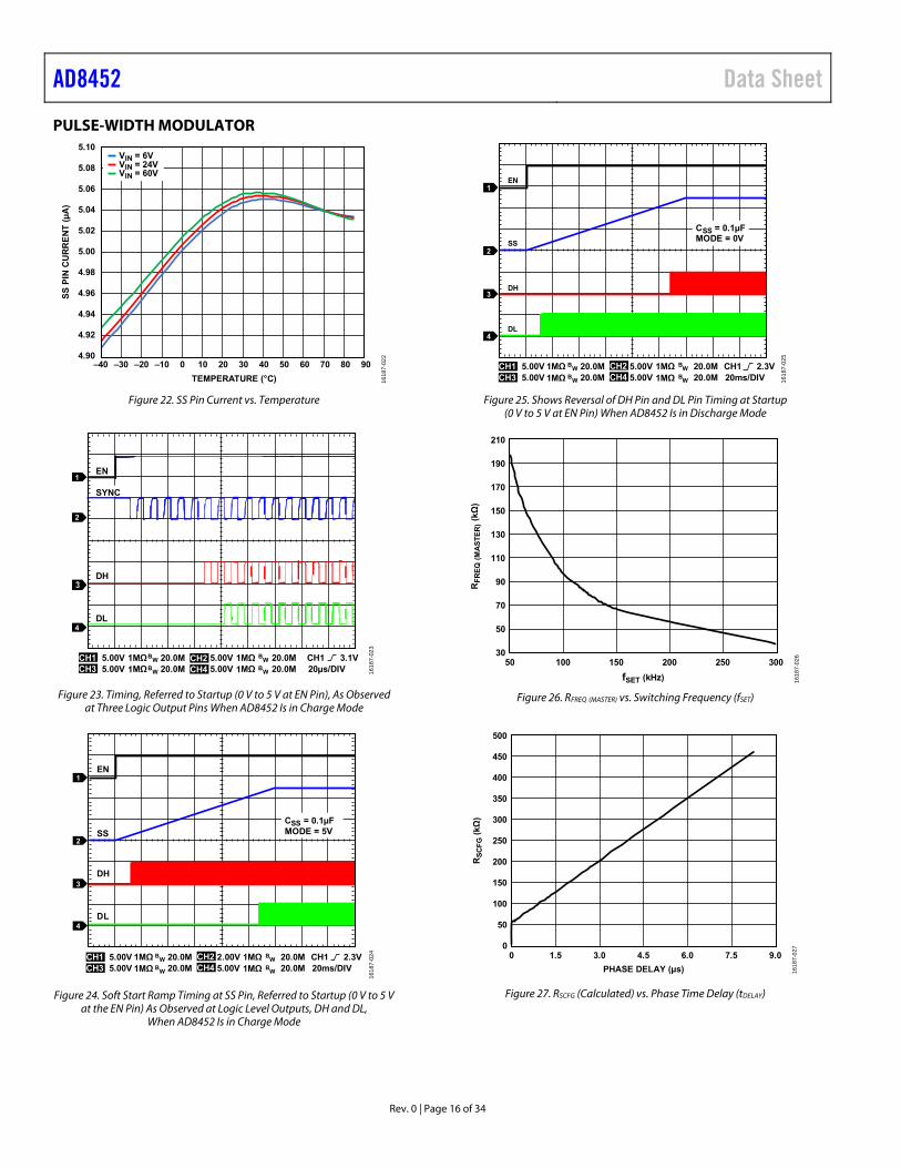
PULSE-WIDTH MODULATOR
TEMPERATURE (°C)
3020 40 50 60 70 80 900–10 10–20–30–40
5.10VIN = 6VVIN = 24VVIN = 60V
SS
PIN
CU
RR
EN
T (
µA
)
5.08
5.06
5.04
5.02
5.00
4.98
4.96
4.94
4.92
4.90
1618
7-02
2
Figure 22. SS Pin Current vs. Temperature
CH1 5.00V 1MΩ 20.0M1MΩ 20.0M
1MΩ 20.0M1MΩ 20.0M 20µs/DIV
CH1 3.1VCH3 5.00V
CH2 5.00VCH4 5.00V
1
2
4
1618
7-02
3
EN
DH
DL
SYNC
BW
BW
BW
BW
Figure 23. Timing, Referred to Startup (0 V to 5 V at EN Pin), As Observed at Three Logic Output Pins When AD8452 Is in Charge Mode
1
2
3
4
1618
7-02
4
CSS = 0.1µFMODE = 5V
CH1 5.00V 1MΩ 20.0M1MΩ 20.0M
1MΩ 20.0M1MΩ 20.0M 20ms/DIV
CH1 2.3VCH3 5.00V
CH2 2.00VCH4 5.00V
EN
DH
DL
SS
BW
BW
BW
BW
Figure 24. Soft Start Ramp Timing at SS Pin, Referred to Startup (0 V to 5 V at the EN Pin) As Observed at Logic Level Outputs, DH and DL,
When AD8452 Is in Charge Mode
1618
7-02
5
1
2
3
4
EN
SS
DH
DL
CSS = 0.1µFMODE = 0V
CH1 5.00V 1MΩ 20.0M1MΩ 20.0M
1MΩ 20.0M1MΩ 20.0M 20ms/DIV
CH1 2.3VCH3 5.00V
CH2 5.00VCH4 5.00V
BW
BW
BW
BW
Figure 25. Shows Reversal of DH Pin and DL Pin Timing at Startup (0 V to 5 V at EN Pin) When AD8452 Is in Discharge Mode
210
30
70
110
150
190
50
90
130
170
50 150100 200 250 300
RF
RE
Q (
MA
ST
ER
) (kΩ
)
fSET (kHz) 1618
7-02
6
Figure 26. RFREQ (MASTER) vs. Switching Frequency (fSET)
0 1.5 3.0 4.5 6.0 7.5 9.0
500
450
400
350
300
250
200
150
100
50
0
RS
CF
G(kΩ
)
PHASE DELAY (µs) 1618
7-02
7
Figure 27. RSCFG (Calculated) vs. Phase Time Delay (tDELAY)

Data Sheet AD8452
Rev. 0 | Page 17 of 34
1618
7-02
8
DEAD TIME (ns)
0
75
150
125
50
100
25
175
700600400300 5002001000
RD
T (
kΩ)
Figure 28. DT Pin Resistance (RDT) vs. Dead Time (tDEAD)
VR
EG
(V
)
INPUT VOLTAGE (V)
6033 5124 42156
5.000
4.998
4.996
4.994
4.992
4.990
4.988
4.986
4.984
T = −40°CT = +25°CT = +85°C
1618
7-02
9
Figure 29. VREG vs. Input Voltage (VIN) at Various Temperatures and No Load
VE
N (
V)
TEMPERATURE (°C)
30 40 50 60 70 80 900 20–10 10–20–30–40
1618
7-03
0
1.26
1.25
1.24
1.23
1.22
1.21
1.20
1.19
1.18
VEN RISINGVEN FALLING
Figure 30. EN Pin Threshold Voltage (VEN) vs. Temperature
QU
IES
CE
NT
CU
RR
EN
T (
mA
)
INPUT VOLTAGE (V)
33 4215 51 60246
2.30T = −40°CT = +25°CT = +85°C2.25
2.20
2.15
2.10
2.05
2.00
1.95
1618
7-03
1
Figure 31. Quiescent Current vs. Input Voltage (VIN) at Various Temperatures, EN Pin Low
VIN
UV
LO
TH
RE
SH
OL
D (
V)
TEMPERATURE (°C)
30 40 50 60 70 80 900 20–10 10–20–30–40
1618
7-03
2
5.9UVLO THRESHOLD RISINGUVLO THRESHOLD FALLING
5.8
5.7
5.6
5.5
5.4
5.3
5.2
Figure 32. Input Voltage (VIN) UVLO Threshold vs. Temperature

AD8452 Data Sheet
Rev. 0 | Page 18 of 34
THEORY OF OPERATION INTRODUCTION Lithium ion (Li-Ion) batteries require an elaborate and time consuming postproduction process known as forming. Battery formation consists of a series of charge/discharge cycles that require precise current and voltage control and monitoring. The AD8452 provides not only the stringent current and voltage accuracy requirements, but also a highly accurate PWM, with logic level DH and DL outputs ready for a half-H bridge configured switch mode power output converter—all in a highly compact 7 mm × 7 mm package.
The analog front end of the AD8452 includes a precision current sense in-amp with gain of 66× ±0.1% and a precision voltage sense difference amplifier with a gain of 0.4 × ±0.1% for battery voltage.
As shown in Figure 38, the AD8452 provides constant CC/CV charging technologies, with transparent internal switching between the two. Typical systems induce predetermined levels
of current into or out of the battery until the voltage reaches a target value. At this point, a set constant voltage is applied across the battery terminals, reducing the charge current until reaching zero.
The AD8452 features a complete PWM including on-board user adjustable features such as clock frequency, duty cycle, clock phasing, current limiting, soft start timing, and multichannel synchronization.
Figure 33 is the block diagram of the AD8452, illustrating the distinct sections of the AD8452, including the in-amp and difference amplifier measurement blocks, loop filter amplifiers, and PWM.
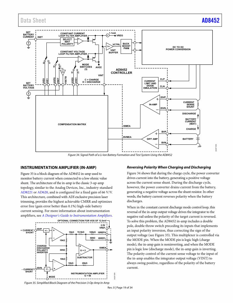
Figure 34 is a block diagram of the AD8452 integrated within a battery formation and test system. The AD8452 is usable over a wide range of current and voltage applications simply by judicious selection of a current sense shunt, selected according to system requirements.
8
7
6
5
4
3
2
9
12
11
10
ISVP
VREG = 5V
ISVN
33
28
27
25
34
AVEE
1
26
35
38
29
ISREFH
VR
EF
ISREFLS
ISREFL
IVE
1
ISM
EA
IVE
0
ISE
T
VIN
T
AG
ND
CL
N
AV
CC
CL
P
VV
E1
VIN
T
VV
E0
VV
P0
VS
ET
CL
VS
ET
B
AVCC
37
BVREFH
BVPS
BVREFL
BVP
BVNS
BVREFLS
EN
BV
ME
A
BVN
MO
DE
500Ω
100kΩ
BATTERYCURRENTSENSE IA
G = 66
SS
MODE_B
31
32
AV
CC
300Ω
60kΩ
AV
EE
AV
EE
36
DH
DL
VIN
CL
VT
SCFG
FA
UL
T
VREG
DT
SS
FREQ
DGND
SYNC
1MΩ
1MΩSS
CL
SS
1×
80kΩ200kΩ
SS DISCHARGE
8.5MΩ
200kΩ
SCFG
SCFG
CONFIGDETECT
30
4V
1×
SYNC
SYNC DETECT
AVEE
AVCC
BATTERYVOLTAGESENSE DAG = 0.4
17 1815 161413 19 20 21 22 23 24
AVEE
CLFLG
AVCC
44 404245 3943 41464748
DMAXDMAX
VREG
DMAX
D
C
DC
D C
MODE'
CLFLG
CLFLG
SYNC
OSCILLATOR
VREG
UVLO
TSD
BANDGAP
MODE_B
5µA
+/–
79.7kΩ
2.5VVREF
1MΩ CURRENT LIMITAND DIODEEMULATION
VS
ET
BU
FF
ER
MODE_B
CV LOOPFILTER
AMPLIFIER
SOFT STARTAMPLIFIER
1.1mA
CC LOOPFILTER
AMPLIFIER
VCTRLCOMP
IDMAX11µA
ISCFG11µA
VBG = 1.252V
MODE_B
DRIVELOGIC
0.3µA
1.64pF
10µA 20µA
20µA
VFREQ = 1.252V
1618
7-03
3
Figure 33. AD8452 Detailed Block Diagram
Data Sheet AD8452
Rev. 0 | Page 19 of 34
BATTERY
VCTRL
CURRENTSENSESHUNT
ISVP
ISVN
BVP
BVN
MODESWITCHES
(3)
BATTERYCURRENT
(IBAT)
AVEE
CONSTANT CURRENTLOOP FILTER AMPLIFIER
1×
VINTBUFFER
VS
ET
B
VS
ET
ISET
CD
CD
CDVINT
ISMEA
BVMEA
VV
E1
VV
E0
VV
P0
AD8452CONTROLLER
SETBATTERYVOLTAGE
SETBATTERYCURRENT
C = CHARGED = DISCHARGE
CONSTANT VOLTAGELOOP FILTER AMPLIFIER
IVE
1
IVE
0BUCKBOOST
PWM
SELECTIBAT
POLARITY
1.1mAVREG
CLP
CLN
CURRENTLIMIT AND
DIODEEMULATION
CHARGE
DISCHARGE
1×
DC TO DCPOWER CONVERSION
COMPENSATION MATRIX
IN-AMP
DIFF AMP
1618
7-03
4
Figure 34. Signal Path of a Li-Ion Battery Formation and Test System Using the AD8452
INSTRUMENTATION AMPLIFIER (IN-AMP) Figure 35 is a block diagram of the AD8452 in-amp used to monitor battery current when connected to a low ohmic value shunt. The architecture of the in-amp is the classic 3-op-amp topology, similar to the Analog Devices, Inc., industry-standard AD8221 or AD620, and is configured for a fixed gain of 66 V/V. This architecture, combined with ADI exclusive precision laser trimming, provides the highest achievable CMRR and optimizes error free (gain error better than 0.1%) high-side battery current sensing. For more information about instrumentation amplifiers, see A Designer's Guide to Instrumentation Amplifiers.
10kΩ
10kΩ 20kΩ
500Ω
INSTRUMENTATION AMPLIFIERG = 66
ISVN
ISVP+ CURRENT
SHUNT
ISMEA
– CURRENTSHUNT
SUBTRACTOR
100kΩ19.5kΩ ISREFH
ISREFL
2.5VVREF
CHARGE/DISCHARGEPOLARITYINVERTER
10kΩ
10kΩ
305Ω
OPTIONAL CONNECTION FOR VOS OF 12.5mV
G = 2
+/–
+/–
1618
7-03
5
Figure 35. Simplified Block Diagram of the Precision 3-Op-Amp In-Amp
Reversing Polarity When Charging and Discharging
Figure 34 shows that during the charge cycle, the power converter drives current into the battery, generating a positive voltage across the current sense shunt. During the discharge cycle, however, the power converter drains current from the battery, generating a negative voltage across the shunt resistor. In other words, the battery current reverses polarity when the battery discharges.
When in the constant current discharge mode control loop, this reversal of the in-amp output voltage drives the integrator to the negative rail unless the polarity of the target current is reversed. To solve this problem, the AD8452 in-amp includes a double pole, double throw switch preceding its inputs that implements an input polarity inversion, thus correcting the sign of the output voltage (see Figure 33). This multiplexer is controlled via the MODE pin. When the MODE pin is logic high (charge mode), the in-amp gain is noninverting, and when the MODE pin is logic low (discharge mode), the in-amp gain is inverting. The polarity control of the current sense voltage to the input of the in-amp enables the integrator output voltage (VINT) to always swing positive, regardless of the polarity of the battery current.

AD8452 Data Sheet
Rev. 0 | Page 20 of 34
In-Amp Offset Option
As shown in Figure 35, the in-amp reference node is connected to the ISREFL pin and ISREFH pin via an internal resistor divider. This resistor divider can be used to introduce a temperature insensitive offset to the output of the in-amp such that it always reads a voltage higher than zero for a zero differential input. Because the output voltage of the in-amp is always positive, a unipolar analog-to-digital converter (ADC) can digitize it.
When the ISREFH pin is tied to the VREF pin with the ISREFL pin grounded, the voltage at the ISMEA pin is increased by an offset voltage, VOS, of 12.5 mV, guaranteeing that the output of the in-amp is always positive for zero differential inputs. Other voltage shifts can be realized by tying the ISREFH pin to an external voltage source. The gain from the ISREFH pin to the ISMEA pin is 5 mV/V. For zero offset, connect the ISREFL pin and ISREFH pin to ground.
Battery Reversal and Overvoltage Protection
The AD8452 in-amp can be configured for high-side or low-side current sensing. If the in-amp is configured for high-side current sensing (see Figure 34) and the battery is connected backward, the in-amp inputs may be held at a voltage that is below the negative power rail (AVEE), depending on the battery voltage.
To prevent damage to the in-amp under these conditions, the in-amp inputs include overvoltage protection circuitry that allows them to be held at voltages of up to 55 V from the opposite power rail. In other words, the safe voltage span for the in-amp inputs extends from AVCC − 55 V to AVEE + 55 V.
DIFFERENCE AMPLIFIER Figure 36 is a block diagram of the difference amplifier used to monitor the battery voltage. The architecture of the difference amplifier is a subtractor amplifier with a fixed gain of 0.4 V/V. This gain value allows the difference amplifier to funnel the voltage of a 5 V battery to a level that can be read by a 5 V ADC with a 4.096 V reference.
BVREFL
BVP
BVN
200kΩ
200kΩ 80kΩ
79.7kΩ
AD8452 DIFFAMP
BVREFH
VREF
BVMEA
300Ω
60kΩ
CONNECTFOR VOS
OF 12.5mV
+ BATTERYTERMINAL
– BATTERYTERMINAL
1618
7-03
6
Figure 36. Difference Amplifier Simplified Block Diagram
The resistors that form the difference amplifier gain network are laser trimmed to a matching level better than ±0.1%. This level of matching minimizes the gain error and gain error drift of the difference amplifier while maximizing the CMRR of the difference amplifier. This matching also allows the controller to set a stable target voltage for the battery over temperature while rejecting the ground bounce in the battery negative terminal.
Like the in-amp, the difference amplifier can also level shift its output voltage via an internal resistor divider that is tied to the difference amplifier reference node. This resistor divider is connected to the BVREFH pin and BVREFL pin.
When the BVREFH pin is tied to the VREF pin with the BVREFL pin grounded, the voltage at the BVMEA pin is increased by 12.5 mV, guaranteeing that the output of the difference amplifier is always positive for zero differential inputs. Other voltage offsets are realized by tying the BVREFH pin to an external voltage source. The gain from the BVREFH pin to the BVMEA pin is 5 mV/V. For zero offset, tie the BVREFL pin and the BVREFH pin to ground.
CC AND CV LOOP FILTER AMPLIFIERS The CC and CV loop filter amplifiers are high precision, low noise specialty amplifiers with very low offset voltage and very low input bias current. These amplifiers serve two purposes:
• Using external components, the amplifiers implement active loop filters that set the dynamics (transfer function) of the CC and CV loops.
• The amplifiers perform a seamless transition from CC to CV mode after the battery reaches its target voltage.
Figure 37 is a functional block diagram of the AD8452 CC and CV feedback loops for charge mode (the MODE pin is logic high). For illustrative purposes, the external networks connected to the loop amplifiers are simple RC networks configured to form single-pole inverting integrators. This type of configuration exhibits very high dc precision when the feedback loop is closed, due to the high loop gain when the feedback loop is in place. The outputs of the CC and CV loop filter amplifiers are internally connected to the VINT pins via an analog NOR circuit (minimum output selector circuit), such that they can only pull the VINT node down. In other words, the loop amplifier that requires the lowest voltage at the VINT pins is in control of the node. Thus, only one loop, CC or CV, can be in control of the system charging control loop at any given time. When the loop is inactive (open, such as when the EN pin is low), the voltage at the VINT pins must be railed at AVCC.

Data Sheet AD8452
Rev. 0 | Page 21 of 34
ISET CC LOOPAMPLIFIER
CV LOOPAMPLIFIER
IVE1
ISVN
BVP
BVN
ISMEA
BVMEA
IA
DA
VVSET
VSET
R1 VISET
MODE
VINT
VINT
ISVP
MINOUTPUTSELECT
VVE1
R2
VSETBUFFER
VSETB
5V
–
+
–
+
–
+–
+
66×
0.4×
C2
C1
IBAT
SHUNT RS
BAT
GH½ BRIDGE AND LPF
GL
IAC
½ BRIDGE DRIVERDH DL
PWMDH
DL
HVAC/12V DCINVERTER/CONVERTER
VCTRL/COMP
1×
1618
7-03
7
Figure 37. Functional Block Diagram of the CC and CV Loops in Charge Mode (MODE Pin High)
The VISET voltage source and VVSET voltage source set the target constant current and the target constant voltage, respectively. When the CC and CV feedback loops are in a steady state, the charging current is set at
IBAT = SIA
ISET
RGV
×
where: IBAT is the steady state charging current. GIA is the in-amp gain. RS is the value of the shunt resistor.
The target voltage is set at
VBAT = DA
VSET
GV
where: VBAT is the steady state battery voltage. GDA is the difference amplifier gain.
Because the offset voltage of the loop amplifiers is in series with the target voltage sources, VISET and VVSET, the high precision of these amplifiers minimizes this source of error.
Charging Lithium-Ion (Li-Ion) Cells
Charging Li-Ion cells is a demonstrably more difficult process than charging most other batteries employing recyclable technologies. The voltage margin of error between optimum storage capacity and damage caused by overcharge is around 1%. Thus, Li-Ion cells are more critical to over/undercharging than any other type battery style, rechargeable or not.
Li-Ion batteries also exhibit the highest energy density per unit of weight and volume than any other style. Such high levels of energy density make them the first choice for portable applications, large and small, from cell phones to high capacity energy storage banks. Realizing their greatest potential requires careful attention to their charge characterization signature.
Concepts of Constant Current (CC) and Constant Voltage (CV)
Batteries can be charged in constant current or constant voltage modes. Figure 38 shows a typical CC/CV multiphase charge profile for a Li-Ion battery. In the first stage of the charging process, the battery is charged with a CC of 1 A. When the battery voltage reaches a target voltage of 4.2 V, the charging process transitions such that the battery is charged with a CV of 4.2 V.
1.25
0
0.25
0.50
0.75
1.00
0 1 2 3 4 5
BA
TTER
Y C
UR
REN
T (A
)
TIME (Hours)
5
4
3
2
1
BA
TTER
Y VO
LTA
GE
(V)
CURRENT (A)VOLTAGE (V)
1A CCCHARGEBEGINS
TRANSITIONFROM 1A CCTO 4.2V CV
VOLTAGERISES TOVSET
VOLTAGERISES TO VSET
CHARGETERMINATES
1618
7-03
8
Figure 38. Representative Li-Ion Battery Charge Profile Showing
Seamless CC to CV Transition
The following sequence of events describes how the AD8452 implements a typical CC/CV charging profile required for a Li-Ion battery. The scenario assumes a newly manufactured, unformed, never before charged battery, and the charge and discharge voltage and current levels along with appropriate time intervals have already been established empirically.
Energy levels (CC, CV, and time intervals are just a small percent of the battery final ratings). For this example, assume a 3.2 V 10 Ah battery is charging at IBAT = 2 A and VBAT = 4.2 V. The process begins with ISET = 66 mV and VSET = 1.68 V, configured for charge mode. Following the target VSET and ISET, the system is enabled by applying a logic high to the EN pin.

AD8452 Data Sheet
Rev. 0 | Page 22 of 34
1. At turn on, the default start-up voltages at the ISMEA pin and BVMEA pin are both zero, and both integrators (loop amplifiers) begin to ramp, increasing the voltage at the VINT node. (The voltage at the VINT pin always rises following an enable regardless of mode setting).
2. As the voltage at the VINT node increases, the output current IBAT from the power converter starts to rise.
3. When the IBAT current reaches the target CC steady state value IBAT, the battery voltage is considerably less than the target steady state value, VBAT. Therefore, the CV loop amplifier forces its output voltage high enough to disconnect itself from VINT. The CC loop prevails, maintaining the target charge current until the target VBAT is achieved and the CC loop stops integrating.
4. Due to the analog OR circuit, the loop amplifiers can only pull the VINT node down. The CC loop takes control of the charging feedback loop, and the CV loop is disabled.
5. As the charging process continues, the battery voltage increases until it reaches the steady state value, VBAT, and the voltage at the BVMEA pin reaches the target voltage, VVSET.
6. The CV loop tries to pull the VINT node down to reduce the charging current (IBAT) and prevent the battery voltage from rising any further. At the same time, the CC loop tries to keep the VINT node at its current voltage to keep the battery current at IBAT.
7. Because the loop amplifiers can only pull the VINT node down due to the analog NOR circuit, the CV loop takes control of the charging feedback loop, and the CC loop is disabled.
The analog OR (minimum output selector) circuit that couples the outputs of the loop amplifiers is optimized to minimize the transition time from CC to CV control. Any delay in the transition causes the CC loop to remain in control of the charge feedback loop after the battery voltage reaches its target value. Therefore, the battery voltage continues to rise beyond VBAT until the control loop transitions; that is, the battery voltage overshoots its target voltage. When the CV loop takes control of the charge feedback loop, it reduces the battery voltage to the target voltage. A large overshoot in the battery voltage due to transition delays can damage the battery; thus, it is crucial to minimize delays by implementing a fast CC to CV transition.
Figure 39 is the functional block diagram of the AD8452 CC and CV feedback loops for discharge mode (MODE logic pin is low). In discharge mode, the feedback loops operate in a similar manner as in charge mode. The only difference is in the CV loop amplifier, which operates as a noninverting integrator in discharge mode. For illustration purposes, the external networks connected to the loop amplifiers are simple RC networks configured to form single-pole integrators.
ISET CC LOOPAMPLIFIER
CV LOOPAMPLIFIER
IVE0ISMEA
BVMEA
IA
DA
VVSET R2
VSET
R1
MODE
VINT
RS
VINT
GH
HALF BRIDGEAND LPF
MINOUTPUTSELECT
VVE0VVP0
R2 C2
VSETBUFFER
VSETB
1×
5V
–
+
–
+
–
+–
+
66×
0.4×
GL
AC IAC
HALF BRIDGEDRIVER
DH DL
PWMDH
DL
INVERTER12V DC
BAT–+
VISET
SHUNT
IBAT
ISVN
BVP
ISVP
BVN
1618
7-03
9
Figure 39. Functional Block Diagram of the CC and CV Loops in Discharge Mode (MODE Pin Low)

Data Sheet AD8452
Rev. 0 | Page 23 of 34
Compensation
In battery formation and test systems, the CC and CV feedback loops have significantly different open-loop gain and crossover frequencies; therefore, each loop requires its own frequency compensation. The active filter architecture of the AD8452 CC and CV loops allows the frequency response of each loop to be set independently via external components. Moreover, due to the internal switches in the CC and CV amplifiers, the frequency response of the loops in charge mode does not affect the frequency response of the loops in discharge mode.
Unlike simpler controllers that use passive networks to ground for frequency compensation, the AD8452 allows the use of feedback networks for its CC and CV loop filter amplifiers. These networks enable the implementation of both proportional differentiator (PD) Type II and proportional integrator differentiator (PID) Type III compensators. Note that in charge mode, both the CC and CV loops implement inverting compensators, whereas in discharge mode, the CC loop implements an inverting compensator, and the CV loop implements a noninverting compensator. As a result, the CV loop in discharge mode includes an additional amplifier, the VSET buffer, to buffer the VSET node from the feedback network VINT buffer.
CHARGE AND DISCHARGE CONTROL Conditions to Charge and Discharge a Battery
Battery charging and discharging requires separate paradigms in terms of the analog requirements and the PWM configurations. These paradigms are based on manufacturer provided information, most importantly the C rating where C is simply the battery capacity expressed in ampere hours. For example, if the battery is C rated as 10 Ah, and the charge rate is specified as 0.2 C, the charge current is 2 A for a duration of 5 hours.
To charge, the applied voltage must be greater than the voltage of the battery under charge and the current must not exceed the manufacturers specification, usually expressed as a fraction of the full C rating. When discharging, the opposite conditions apply; the discharge voltage must be less than the unloaded battery voltage, and the current flows out of the battery, reversing the polarity of the shunt voltage.
Multiple charge/discharge sequences can last for days at a time before the battery achieves its optimum storage capacity, and the charge/discharge currents and voltages must be accurately monitored.
MODE Pin
The MODE pin is a logic level input that selects charge with a logic high (VMODE > 2 V) or discharge with a logic low (VMODE < 0.8 V). All the analog and PWM circuitry for charging and discharging of the battery is configured and is latched in when the EN pin goes high.
The MODE pin controls the polarity of the internal analog loop and the DH/DL sequence. In charge mode, DH precedes DL; in discharge mode, DL precedes DH.
When the AD8452 operates in charge mode, the PWM operates in a buck configuration. In discharge mode, the configuration changes to boost. See Figure 40 and Figure 41 for the AD8452 DH and DL behavior in each mode. On the rising edge of EN, the state of the MODE pin is latched, preventing the mode of operation from being changed while the device is enabled. To change between charge and discharge modes of operation, shut down or disable the AD8452, adjust the MODE pin to change the operating mode, and reenable the system.
The operating mode can be changed when the EN pin is driven low, the FAULT pin is driven low, or the AD8452 is disabled via a TSD event or UVLO condition. On the rising edge of the FAULT control signal, the state of the MODE pin is latched, preventing the mode of operation from being changed while the device is enabled.
4.5V
VREG(5V TYP)
0.5V0V
PIN DL
2.5V (TYP)
PIN DH
INTERNAL RAMP(4V p-p)
VREG(5V TYP)
DH AND DL IN CHARGE MODE
0V
0V
1618
7-04
0
Figure 40. DH and DL Output Waveforms for Charge Mode
4.5V
VREG(5V TYP)
0.5V0V
PIN DL
2.5V (TYP)
PIN DH
INTERNAL RAMP(4V p-p)
VREG(5V TYP)
DH AND DL IN DISCHARGE MODE
0V
0V
1618
7-04
1
Figure 41. DH and DL Output Waveforms for Discharge Mode
INPUT AND OUTPUT SUPPLY PINS The AD8452 has five power supply input pins, a pair each of the internally connected AVCC pin and AVEE pin for the analog section and Input VIN for the PWM section. The maximum supply voltage for the VIN pin is 60 V; if operating with an input voltage greater than 50 V, see Figure 42 for recommended additional input filtering.
SUPPLY > 50VAD8452
R
4.7µF
VIN
C
1618
7-04
2
Figure 42. Recommended Filter Configuration for
Input Voltages Greater Than 50 V

AD8452 Data Sheet
Rev. 0 | Page 24 of 34
For optimum protection from switching and other ambient noise, all of these supply pins must be bypassed to ground with high quality ceramic capacitors (X7R or better), located as near as possible to the device.
VREG is an internal 5 V supply that powers the control circuitry including all the current sources for user selected PWM features. It is active as long as VIN is above the internal UVLO (5.75 V typical). VREG may be used as a pull-up voltage for the MODE, SYNC, DMAX, and FAULT pins and any other external pull-ups as long as the additional current does not exceed 5 mA. Bypass the VREG pin to ground with a 1 μF ceramic capacitor.
SHUTDOWN The EN input turns the AD8452 PWM section on or off and can operate from voltages up to 60 V. When the EN voltage is less than 1.2 V (typical), the PWM shuts down, and DL and DH are driven low. When the PWM shuts down, the VIN supply current is 15 μA (typical). When the EN voltage is greater than 1.26 V (typical), the PWM is enabled.
In addition to the EN pin, the PWM is disabled via a fault condition flagged by an TSD, an undervoltage lockout (UVLO) condition on VIN, or an external fault condition via the FAULT pin.
When changing the operating mode, it is necessary to disable the AD8452 by setting the EN pin low.
UNDERVOLTAGE LOCKOUT (UVLO) The UVLO function prevents the PWM from turning on until voltage VIN ≥ 5.75 V (typical). The UVLO enable state has ~410 mV of hysteresis to prevent the PWM from turning on and off repeatedly if the supply voltage to the VIN pin ramps slowly. The UVLO disables the PWM when VIN drops below 5.34 V (typical).
SOFT START The AD8452 has a programmable soft start that prevents output voltage overshoot during startup. When the EN pin goes high, an internal 5 μA current source connected to the SS pin begins charging the external capacitor, CSS, that is connected to VREG (5 V), creating a linear voltage ramp (VSS) that controls several time sensitive PWM control functions.
When VSS < 0.52 V (typical), the DH and DL logic outputs are both low. When VSS exceeds 0.52 V (typical), nonsynchronous switching is enabled, either the DH pin or the DL pin logic output become active, and the PWM duty cycle gradually increases. When VSS > 4.5 V (typical), synchronous switching is enabled (see Figure 43 and Figure 44).
1618
7-04
3
4.5V
0.52V0V
EN
5V
SSSYNCHRONOUS OPERATIONENABLED AT ~90% RAMP
PWM SWITCHINGENABLED AT ~10% RAMPBEGIN
RAMP
EN GOES HIGH0V
5V
DL5V
DH5V
DL FOLLOWS
DH BEGINS
Figure 43. DH and DL Sequence in Charge Mode
DL5V
DH5V
DL FOLLOWS
DH BEGINS
1618
7-04
4EN
SYNCHRONOUS OPERATIONENABLED AT ~90% RAMP
PWM SWITCHINGENABLED AT ~10% RAMP
EN GO ES HIGH0V
5V
4.5V
0.52V0V
5V
SS
BEGINRAMP
Figure 44. DH and DL Sequence in Discharge Mode
In conjunction with the MODE pin, the VSS ramp also establishes when the DH and DL, logic outputs and thus the output FET switches, become active. In charge mode (Mode high), the pulse sequence at the DH pin precedes that at the DL pin. Conversely, in discharge mode, the sequence is reversed and the DL pin precedes the DH pin.
The duty cycle of the DH and DL drive pins increase in proportion to the ramp level, reducing the output voltage overshoot during startup (see the Selecting CSS section).

Data Sheet AD8452
Rev. 0 | Page 25 of 34
UPPER SWITCHGATE DRIVE (DH)
SOFT START(PIN SS)
CURRENT LIMITTHRESHOLD
(VCLVT)
REPEATED CURRENTLIMIT VIOLATION
DETECTED FOR UPTO 16 COUNTS
COOL DOWN
PIN SS GOES LOWAND NORMAL SOFT START
(SS) BEGINS
CURRENTLIMIT FLAG
(PIN CLFLG)
0V
RESETCURRENT-LIMIT
NORMALSOFT STARTSEQUENCE
IRCL
PIN DH AND PIN DL GO LOWFOR 16 COUNTS
5V
0V
t
1618
7-04
6
Figure 45. Recovery from a Peak Current-Limit Event
PWM DRIVE SIGNALS The AD8452 has two 5 V logic level output drive signals, DH and DL, that are compatible with MOSFET drivers such as the ADuM3223 or ADuM7223. The DH and DL drive signals synchronously turn on and off the high-side and low-side switches driven from the external driver. The AD8452 provides a resistor programmable dead time to prevent the DH pin and DL pin from transitioning at the same time, as shown in Figure 46. Connect a resistor from the DT pin to ground to program the dead time.
DL
DH
tDEADtDEAD
1618
7-04
5
Figure 46. Dead Time (tDEAD) Between DH and DL Transitions
When driving capacitive loads with the DH and DL pins, a 20 Ω resistor must be placed in series with the capacitive load to reduce ground noise and ensure signal integrity.
PEAK CURRENT PROTECTION AND DIODE EMULATION (SYNCHRONOUS) Peak Current-Limit Detection
The AD8452 provides an adjustable peak current limit for fast response to overcurrent conditions. When the peak current limit is reached, the main switching FET is turned off, limiting the peak current for the switching cycle and the CLFLG pin is driven low. When the peak inductor current exceeds the programmed current limit for more than 16 consecutive clock cycles, a peak current overload condition occurs. If the current overload condition exists for less than 16 consecutive cycles, the counter is reset to zero and the peak current overload condition is avoided. During the peak current-limit condition, the SS capacitor is discharged to ground, and the drive signals (DL and DH) are disabled for the next 16 clock cycles to allow the FETs to cool down (current overload mode). When the 16 clock cycles expire, the AD8452 restarts with a new soft start cycle. Figure 45 shows the sequence for a peak current-limit event.
As shown in Figure 47, the inductor current, IRCL ,is sensed by a low value resistor, RCL (for example, 5 mΩ), placed between the output inductor and capacitor. The IRCL current is bidirectional, depending on whether the AD8452 is in charge or discharge mode. The MODE pin automatically controls the polarity of the voltage sampled across RCL to set the peak current-limit detection. Because the average output voltage at the junction of the low-pass filter inductor and capacitor is equal to the battery potential, the common-mode voltage is rejected, leaving only the desired differential result.

AD8452 Data Sheet
Rev. 0 | Page 26 of 34
PEAK CURRENT LIMITINGAND DIODE EMULATION
VREG
(CLP – CLN)
VREG
MODE
DL
DH
CLVT
ICLVT = 20µA
RCLVT
V1mV
AD8452
DUTY CYCLE DH
DUTY CYCLE DL
CUR LIM
SYNC OFF
CLNCLP
+DCBUS
VRCL
RCL
IRCL
VBATRSH
VCLVT
1618
7-04
7
+ –
Figure 47. Peak Current Limiting and Diode Emulation Block Diagram
The threshold voltage for the peak current comparator is user adjustable by connecting a resistor from the current-limit voltage threshold (CLVT pin) to ground. The AD8452 generates this voltage from a 20 μA current source (see the Select RCL and RCLVT for the Peak Current Limit section).
Diode Emulation/Synchronous Mode Operation
The RCL current sense resistor is also used to detect and control current reversal. When the voltage across RCL drops to −5 mV ≤ VRCL ≤ +5 mV (for charge and discharge modes) during the synchronous FET switching cycle, the synchronous FET is turned off to stop the flow of reverse current.
Information on how to set the current limit and the current sense resistor RCL is available in the Applications Information section.
2.5A
0A
DL
DH
2.5A p-p
DH AND DL WITH INDUCTOR CURRENTWHILE IN CHARGE MODE
DIODEEMULATION
BEGINS
INDUCTORCURRENT
1618
7-04
8
Figure 48. Diode Emulation in Charge Mode, Low Charge Current Required
FREQUENCY AND PHASE CONTROL The FREQ, SYNC, and SCFG pins determine the source, frequency, and synchronization of the clock signal that operates the PWM control of the AD8452.
Internal Frequency Control
The AD8452 frequency can be programmed with an external resistor connected between FREQ and ground. The frequency range can be set from a minimum of 50 kHz to a maximum of 300 kHz. If the SCFG pin is tied to VREG, forcing VSCFG ≥ 4.53 V (typical), or if the SCFG pin is left floating, the SYNC pin is configured as an output, and the AD8452 operates at the frequency set by RFREQ, which outputs from the SYNC pin through the open-drain device. The output clock of the SYNC pin operates with a 50% (typical) duty cycle. In this configuration, the SYNC pin can synchronize other switching regulators in the system to the AD8452. When the SYNC pin is configured as an output, an external pull-up resistor is needed from the SYNC pin to an external supply. The VREG pin of the AD8452 can be used as the external supply rail for the pull-up resistor.
External Frequency Control
When VSCFG ≤ 0.5 V (typical), the SYNC pin is configured as an input, the AD8452 synchronizes to the external clock applied to the SYNC pin, and the AD8452 operates as a slave device. This synchronization allows the AD8452 to operate at the same switching frequency with the same phase as other switching regulators or devices in the system. When operating the AD8452 with an external clock, select RFREQ to provide a frequency that approximates but is not equal to the external clock frequency, which is further explained in the Applications Information section.
Operating Frequency Phase Shift
When the voltage applied to the SCFG pin is 0.65 V < VSCFG < 4.25 V, the SYNC pin is configured as an input, and the AD8452 synchronizes to a phase shifted version of the external clock applied to the SYNC pin. To adjust the phase shift, place a resistor (RSCFG) from SCFG to ground. The phase shift can be used to reduce the input supply ripple for systems containing multiple switching power supplies.
MAXIMUM DUTY CYCLE Referring to Figure 52, the maximum duty cycle of the AD8452 can be externally programmed for any value between 0% and 97% by installing a resistor from the DMAX pin to ground. The maximum duty cycle defaults to 97% if the DMAX pin is left floating or connected to 5 V (the VREG pin).

Data Sheet AD8452
Rev. 0 | Page 27 of 34
FAULT INPUT
The AD8452 FAULT pin is a logic level input intended to be driven by an external fault detector. The external fault signal stops PWM operation of the system to avoid damage to the application and components. When a voltage of less than 1.0 V (typical) is applied to the FAULT pin, the AD8452 is disabled, driving the DL and DH PWM drive signals low. The soft start capacitor (CSS) is discharged through a switch until a voltage ≥1.2 V is applied to the FAULT pin, and the AD8452 resumes switching. The FAULT pin sustains voltages as high as 60 V.
THERMAL SHUTDOWN (TSD) The AD8452 has a TSD protection circuit. The TSD triggers and disables switching when the junction temperature reaches 150°C (typical). While in TSD, the DL and DH signals are driven low, the CSS capacitor discharges to ground, and VREG remains high. Normal operation resumes when the junction temperature decreases to 135°C (typical).

AD8452 Data Sheet
Rev. 0 | Page 28 of 34
APPLICATIONS INFORMATION ANALOG CONTROLLER This section describes how to use the AD8452 in the context of a battery formation and test system and includes design examples.
FUNCTIONAL DESCRIPTION The AD8452 is a precision analog front end and controller for battery formation and test systems. Such systems are differentiated from typical battery charger or battery management systems by the high level of voltage and current measurement precision required to optimize Li-Ion batteries for capacity and energy density. Figure 49 shows the analog signal path of a simplified switching battery formation and test system using the AD8452 controller.
The AD8452 is suitable for systems that test and form Li-Ion and the legacy NiCad and NiMH electrolyte batteries. The output is a digital format (PWM), designed to drive a switching power output stage.
The AD8452 includes the following blocks (see Figure 33 and the Theory of Operation section for more information):
• A fixed gain in-amp that senses low-side or high-side battery current.
• A fixed gain difference amplifier that measures the terminal voltage of the battery.
• Two loop filter error amplifiers that receive the battery target current and voltage and establish the dynamics of the CC and CV feedback loops.
• A minimum output selector circuit that combines the outputs of the loop filter error amplifiers to perform automatic CC to CV switching.
• A PWM with high- and low-side half bridge logic level outputs suitable for driving a MOSFET gate driver.
• A 2.5 V reference whose output node is the VREF pin. • A logic input pin (MODE) that switches the controller
configuration between charge mode (high) and discharge mode (low).
BATTERY
VCTRL
CURRENTSENSESHUNT
CLP
CLN
BVP
BVN
MODESWITCHES
(3)
BATTERYCURRENT
(IBAT)
AVEE
CONSTANT CURRENTLOOP FILTER AMPLIFIER
1×VINT
BUFFER
VSET
B
VSET
ISET
CDCD
CDVINT
ISMEA
BVMEA
VVE1
VVE0
VVP0
AD8452CONTROLLER
SETBATTERYVOLTAGE
SETBATTERYCURRENT
COMPENSATIONMATRIX
C = CHARGED = DISCHARGE
CONSTANT VOLTAGELOOP FILTER AMPLIFIER
IVE1
IVE0
C
D
D
D
C
D
D
D
C
C
AVCC
DC TO DCPOWER CONVERSION
BUCKBOOSTPWM
LEVELSHIFTER
SELECTIBAT
POLARITY
1.1mAVREG
ISVP
ISVN
OUTPUTSWITCHES
LPF
CURRENTLIMIT AND
DIODEEMULATION
RCL
1×
PGDA
PGIA
1618
7-04
9
Figure 49. Complete Signal Path of a Battery Test or Formation System Suitable for Li-Ion Batteries

Data Sheet AD8452
Rev. 0 | Page 29 of 34
POWER SUPPLY CONNECTIONS The AD8452 requires three analog power supplies (AVCC, VIN, and AVEE). Two separate ground pins, AGND and DGND, provide options for isolating analog and digital ground paths in high noise environments. In most applications, however, these two pins can be connected to a common ground.
AVCC and AVEE power all the analog blocks, including the in-amp, difference amplifier, and op amps. VIN powers an internal 5 V LDO regulated supply (VREG) that powers the mode logic and PWM.
The rated absolute maximum value for AVCC − AVEE is 36 V, and the minimum operating AVCC and AVEE voltages are +10 V and −26 V, respectively. Due to the high PSRR of the AD8452 analog circuitry, the AVCC pin can be connected directly to the high current power bus (the input voltage of the power converter) without risking injection of supply noise to the controller outputs.
A commonly used power supply combination is +12 V for AVCC and −5 V for AVEE. The 12 V rail for AVCC provides enough headroom to the in-amp such that it can be connected in a high-side current sensing configuration. The −5 V AVEE rail allows the difference amplifier output to become negative if the battery under test (BUT) is accidentally connected in reverse. The condition can be detected by monitoring BVMEA for reverse voltage.
It is good practice to connect decoupling capacitors to all the supply pins. A 1 µF ceramic capacitor in parallel with a 0.1 µF capacitor is recommended.
CURRENT SENSE IN-AMP CONNECTIONS For a description of the instrumentation amplifier, see the Theory of Operation section, Figure 33, and Figure 35. The in-amp fixed gain is 66 V/V.
Current Sensors
Two common options for current sensors are isolated current sensing transducers and shunt resistors. Isolated current sensing transducers are galvanically isolated from the power converter and are affected less by the high frequency noise generated by switch mode power supplies. Shunt resistors are far less expensive, easier to deploy and generally more popular.
If a shunt resistor sensor is used, a 4-terminal, low resistance shunt resistor is recommended. Two of the four terminals conduct the battery current, whereas the other two terminals conduct virtually no current. The terminals that conduct no current are sense terminals that are used to measure the voltage drop across the resistor (and, therefore, the current flowing through it) using an amplifier such as the in-amp of the AD8452. To interface the in-amp with the current sensor, connect the sense terminals of the sensor to the ISVP pin and ISVN pin of the AD8452 (see Figure 50).
Optional Low-Pass Filter
Due to the extremely high impedance of the instrumentation amplifier used for a current shunt amplifier, power stage switching noise can become an issue if the input circuitry is in close proximity to the power stage components. This issue is mitigated by shielding the input leads with ground potential shielding designed into the PCB artwork and keeping the input leads close together between the current sense shunt and the input pins.
Connecting an external differential low-pass filter between the current sensor and the in-amp inputs is also an effective method to reduce the injection of switching noise into the in-amp (see Figure 50).
ISVP
10kΩ
10kΩ 20kΩ
20kΩ
4-TERMINALSHUNT
IBAT
BATTERYUNTER TEST
ISVN
10kΩ
10kΩ
305ΩIMEAS
+
–
OPTLPF
1618
7-05
0
Figure 50. 4-Terminal Shunt Resistor Connected to the Current Sense In-Amp
VOLTAGE SENSE DIFFERENTIAL AMPLIFIER CONNECTIONS For a description of the difference amplifier, see the Theory of Operation section, Figure 33, and Figure 36. The gain of the difference amplifier is fixed at 0.4×. For AD8452 applications in large installations, the best practice is to connect each battery with a dedicated pair of conductors to avoid accuracy issues. This recommendation applies whether using wiring harnesses or a distributed PCB approach (mother/ daughter boards) to the system design.
BATTERY CURRENT AND VOLTAGE CONTROL INPUTS (ISET AND VSET) The voltages at the ISET pin and the VSET pin set the target battery current and voltage (CC mode and CV mode) and require highly accurate and stable voltages to drive them. For a locally controlled system, a low noise LDO regulator such as the ADP7102ARDZ-5.0 is appropriate. For large scale computer controlled systems, a digital-to-analog converter (DAC) such as the dual channel, 16-bit AD5689RBRUZ is suitable for these purposes. In either event, the source output voltage and the in-amp and difference amplifier reference pins (ISREFH/ISREFL and BVREFH/BVREFL, respectively) must use the same ground reference. For example, if the in-amp reference pins are connected to AGND, the voltage source connected to ISET must also be referenced to AGND. In the same way, if the difference amplifier

AD8452 Data Sheet
Rev. 0 | Page 30 of 34
reference pins are connected to AGND, the voltage source connected to VSET must also be referenced to AGND.
In constant current mode, when the CC feedback loop is in a steady state, the ISET input sets the battery current as follows:
IBAT = SIA
ISET
RGV×
= S
ISET
RV×66
where: GIA is the in-amp gain. RS is the value of the current sense resistor.
Note that the system accuracy is highly dependent on the physical properties of the shunt as well as the in-amp GIA and VISET values. When selecting a shunt, be sure to consider temperature performance as well as basic precision.
In constant voltage mode, when the CV feedback loop is in a steady state, the VSET input sets the battery voltage according to the equation:
VBAT = DA
VSET
GV
= 4.0
VSETV
where GDA is the difference amplifier gain.
Therefore, the accuracy and temperature stability of the formation and test system are not only dependent on the accuracy and stability of the AD8452 but also on the accuracy external components.
LOOP FILTER AMPLIFIERS The AD8452 has two loop filter amplifiers, also known as error amplifiers (see Figure 49). One amplifier is for constant current control (CC loop filter amplifier), and the other amplifier is for constant voltage control (CV loop filter amplifier). The outputs of these amplifiers are combined using a minimum output selector circuit to perform automatic CC to CV switching.
Table 9 lists the inputs of the loop filter amplifiers for charge mode and discharge mode.
Table 9. Integrator Input Connections
Feedback Loop Function Reference Input
Feedback Terminal
Control the Current While Discharging a Battery
ISET IVE0
Control the Current While Charging a Battery
ISET IVE1
Control the Voltage While Discharging a Battery
VSET VVE0
Control the Voltage While Charging a Battery
VSET VVE1
The CC and CV amplifiers in charge mode and the CC amplifier in discharge mode are inverting integrators, whereas the CV amplifier in discharge mode is a noninverting integrator. Therefore, the CV amplifier in discharge mode uses an extra amplifier, the VSET buffer, to buffer the VSET input pin (see Figure 33). In addition, the CV amplifier in discharge mode uses the VVP0 pin to couple the signal from the BVMEA pin to the integrator.
SELECTING CHARGE OR DISCHARGE OPTIONS To operate the AD8452 in discharge mode (including energy recycling) mode, apply a voltage less than 1.05 V (typical) to the MODE pin. To operate the AD8452 in charge mode, drive the MODE pin high, greater than 1.20 V (typical). The state of the MODE pin can change when the AD8452 is shut down via the EN pin or via an external fault condition signaled on the FAULT pin, a TSD event, or an UVLO condition.
SELECT RCL AND RCLVT FOR THE PEAK CURRENT LIMIT Figure 47 is the block diagram for peak current limit and diode emulation. Note that the current-limit sense resistor is floating between the output filter inductor and capacitor.
The current generated by a fault condition defines the peak current. In turn, the peak current equals the sum of the average current (rated battery charging or discharging current) and the peak incremental inductor current:
IPK = IAVG + IMAX
where: IAVG is the battery charge/discharge current. ILMAX is the the inductor saturation current.
Typically, the peak current level is set to the sum of the average current and the value of the inductor saturation current.
Use the following equation to calculate the minimum current-limit sense resistor value:
RCL MIN (Ω) = )(
mV50AI PK
(2)
where: IPK is the desired peak current limit in A. RCL MIN is the minimum current limit sense resistor value in Ω. 50 mV is the minimum IR drop across RCL for sufficient noise immunity during operation.
Select the next higher standard resistor value for RCL.
Next, the value for RCLVT is calculated using the following equation:
RCLVT (Ω) =
×
CLVT
CLPKI
RI (3)
where: RCLVT is the current-limit threshold voltage resistor value in Ω. IPK is the desired peak current limit in A. RCL is the current-limit sense resistor value in Ω. ICLVT is the CLVT pin current (21 µA typical)
The AD8452 is designed so that the peak current limit is the same in both the buck mode and the boost mode of operation. A 1% or better tolerance for the RCL and RS resistors is recommended.

Data Sheet AD8452
Rev. 0 | Page 31 of 34
SETTING THE OPERATING FREQUENCY AND PROGRAMMING THE SYNCHONIZATION PIN Operating modes of the AD8452 clock rely on the state of the FREQ pin and one of three possible voltage options applied to the SCFG pin. See Table 10 for a summary of synchronization options.
When the voltage at the SCFG pin exceeds 4.53 V (or the pin is floating and internally connected to VREG), the AD8452 operates at the frequency set by RFREQ. The SYNC pin is configured as an output, displaying a clock signal at the programmed frequency. In this state, the clock voltage at the SYNC pin can be used as a master clock for synchronized applications.
If VSCFG is ≤0.5 V, the SYNC pin is configured as an input, and the AD8452 operates as a slave device. As a slave device, the AD8452 synchronizes to the external clock applied to the SYNC pin. If the voltage applied to the SCFG pin is 0.65 V < VSCFG < 4.25 V, and a resistor is connected between SCFG and ground, the SYNC pin is configured as an input, and the AD8452 synchronizes to a phase shifted version of the external clock applied to the SYNC pin.
Whether operating the AD8452 as a master or as a slave device, carefully select RFREQ using the equations in the following sections.
Select RFREQ for Standalone or Master Clock
Whether master or slave, the clock frequency can be selected graphically or by applying Equation 4.
Figure 26 shows the relationship between the RFREQ (MASTER) value and the programmed switching frequency. Simply identify the desired clock frequency on Axis fSET, and read the corresponding resistor value on Axis RFREQ (MASTER).
To calculate the RFREQ (MASTER) value for a desired master clock synchronization frequency, use the following equation:
( )(kHz)
10kΩ4
)(SET
MASTERFREQ fR = (4)
where RFREQ (MASTER) is the resistor in kΩ to set the frequency for the master device, and fSET is the switching frequency in kHz.
Selecting RFREQ for a Slave Device
To configure the AD8452 as a slave device, drive VSCFG < 4.53 V, and the device operates at the frequency of an external clock applied to the SYNC pin. To ensure proper synchronization, select RFREQ to set the frequency to a value slightly slower than that of the master clock by using the following equation:
RFREQ (SLAVE) = 1.11 × RFREQ (MASTER) (5)
where RFREQ (SLAVE) is the resistor value that appropriately scales the frequency for the slave device, 1.11 is the RFREQ slave to master ratio for synchronization and RFREQ (MASTER) is the resistor value of the master clock applied to the SYNC pin.
The frequency of the slave device is set to a frequency slightly lower than that of the master device to allow the digital synchronization loop of the AD8452 to synchronize to the
master clock period. The slave device can synchronize to a master clock frequency running from 2% to 20% higher than the slave clock frequency. Setting RFREQ (SLAVE) to 1.11× larger than RFREQ (MASTER) runs the synchronization loop in approximately the center of the adjustment range.
Programming the External Clock Phase Shift
If a phase shift is not required for slave devices, connect the SCFG pin of each slave device to ground. For devices that require a phase shifted version of the synchronization clock that is applied to the SYNC pin of the slave devices, connect a resistor (RSCFG) from SCFG to ground to program the desired phase shift. To determine the RSCFG value for a desired phase shift (φSHIFT), start by calculating the frequency of the slave clock (fSLAVE).
(SLAVE)FREQSLAVE R
f410(kHz) = (6)
Next, calculate the period of the slave clock.
3
(kHz)101s)( ×=µ
SLAVESLAVE f
t (7)
where: tSLAVE is the period of the slave clock in µs. fSLAVE is the frequency of the slave clock in kHz.
Next, determine the phase time delay (tDELAY) for the desired phase shift (φSHIFT) using the following equation:
( )360
μss)( SHIFT SLAVE
SLAVEt
t×ϕ
=µ (8)
where: tDELAY is the phase time delay in µs. φSHIFT is the desired phase shift.
Lastly, use the following equation to calculate tDELAY:
RSCFG (kΩ) = 0.45 × RFREQ (SLAVE) (kΩ) + 50 × tDELAY (µs) (9)
where: RSCFG is the corresponding resistor for the desired phase shift in kHz. See Figure 27 for the RSCFG vs. tDELAY graph.
When using the phase shift feature, connect a capacitor of 47 pF or greater in parallel with RSCFG.
Alternatively, the SCFG pin can be controlled with a voltage source but if an independent voltage source is used, ensure VSCFG ≤ VREG under all conditions. When the AD8452 is disabled via UVLO, VREG = 0 V, and the voltage source must be adjusted accordingly to ensure VSCFG ≤ VREG.

AD8452 Data Sheet
Rev. 0 | Page 32 of 34
Table 10. Summary of Synchronization Options of the AD8452
DC Control Bias Applied to the SCFG Pin (V)
SYNC Pin Input/Output State and Delay Options
Master/Slave Sync Input/ Output Delay
0 to 0.50 Input No delay Slave
0.65 to 4.25 Input 0 μs to 7.5 μs delay (see Figure 27) Slave
4.53 to 5 Output No delay Master
Figure 51 shows the internal voltage ramp of the AD8452. The voltage ramp is a well controlled 4 V p-p.
4.5V
0.5V0V
4V p-p
0.03T
0.97T
T
1618
7-05
1
Figure 51. Internal Voltage Ramp
Programming the Dead Time
To adjust the dead time on the synchronous DH and DL outputs, connect a resistor (RDT) from DT to DGND and bypass with a 47 pF capacitor. Select RDT for a given dead time using Figure 28 or calculate RDT using the following equations. To create a single equation for RDT, combine the equations for VDT and RDT.
76.3)00.10(ns)(
)(−×
= DEADDTDT
tIVV (10)
DT
DTDT I
VR = (11)
where: VDT is the DT pin programming voltage. IDT is the 20 µA (typical) internal current source. tDEAD is the desired dead time in ns. RDT is the resistor value in kΩ for the desired dead time.
To calculate RDT for a given tDEAD, the resulting equation used is
76.300.10(ns)
)(−
=Ω DEADDT
tkR (12)
PROGRAMMING THE MAXIMUM DUTY CYCLE The AD8452 is designed with a 97% (typical) maximum internal duty cycle. By connecting a resistor from DMAX to ground, the maximum duty cycle can be programmed at any value from 0% to 97% by using the following equation:
( ) 5.105.21
% −××
=FREQ
DMAXFREQMAX R
RVD (13)
where: DMAX is the programmed maximum duty cycle. VFREQ = 1.252 V (typical). RDMAX is the value of the resistance used to program the maximum duty cycle. RFREQ is the frequency set resistor used in the application.
The DMAX current source is equivalent to the programmed current of the FREQ pin:
FREQ
FREQFREQDMAX R
VII == (14)
where IDMAX = IFREQ, the current programmed on the FREQ pin.
450
00 100
RD
MA
X (k
Ω)
DUTY CYCLE (%)
100
50
200
150
250
300
350
400
6020 8040
TA = +25°C
MAXIMUMDUTY CYCLE
97%
MAXIMUMRESISTOR VALUE(APPROX 400kΩ)
1618
7-05
2
Figure 52. RDMAX vs. Duty Cycle, RFREQ = 100 kΩ, VINT = 5 V
The default maximum duty cycle of the AD8452 is 97% (typical) even if the value of RDMAX indicates a larger percentage. If a 97% internal maximum duty cycle is sufficient for the application, the DMAX pin may be pulled to VREG or left floating.
The CDMAX capacitor connected from the DMAX pin to the ground plane must be 47 pF or greater.

Data Sheet AD8452
Rev. 0 | Page 33 of 34
SELECTING CSS There are instances where it is useful to adjust the soft start delay to fit specific applications, for example, to accommodate charge or discharge battery characteristics, and the state of charge. The soft start delay is user adjustable by selecting the value of Capacitor CSS.
When the EN pin goes high, and with a capacitor connected to the SS pin, a 5 μA current source, ISS, becomes active and begins charging CSS, initiating a timing ramp determined by the following equation:
I = C dV/dt
In the limit, dV = 5 V and, because the applied current is 5 μA, CSS can be calculated for any desired time by transposing the terms of the equation. Therefore,
CSS = I(dt/dV)
For a 1 sec delay, CSS = 5 e – 6(1/5) or 1 μF, a 0.5 sec delay requires 0.5 μF, and so on.
ADDITIONAL INFORMATION The following reference materials provide additional insight and practical information that supplement the data sheet material contained herein:
AN-1319 Application Note, Compensator Design for a Battery Charge/Discharge Unit Using the AD8450 or the AD8451.
AD8452-EVALZ (UG-1180), Universal Evaluation Board for the AD8452. The AD8452-EVALZ has an embedded AD8452 with reference and test loops and is designed for product evaluation and experimenters.
AD8452 System Demo User Guide (UG-1181), AD8452 Battery Testing and Formation Evaluation Board. This user guide features plug and play complete on one channel and a working system, including PC control.

AD8452 Data Sheet
Rev. 0 | Page 34 of 34
OUTLINE DIMENSIONS
COMPLIANT TO JEDEC STANDARDS MS-026-BBC
TOP VIEW(PINS DOWN)
1
1213
2524
363748
0.270.220.17
0.50BSC
LEAD PITCH
1.60MAX
0.750.600.45
VIEW A
PIN 1
0.200.09
1.451.401.35
0.08COPLANARITY
VIEW AROTATED 90° CCW
SEATINGPLANE
7°3.5°0°0.15
0.05
9.209.00 SQ8.80
7.207.00 SQ6.80
0517
06-A
Figure 53. 48-Lead Low Profile Quad Flat Package [LQFP]
(ST-48) Dimensions shown in millimeters
ORDERING GUIDE Model1 Temperature Range Package Description Package Option AD8452ASTZ −40°C to +85°C 48-Lead Low Profile Quad Flat Package [LQFP] ST-48 AD8452ASTZ-RL −40°C to +85°C 48-Lead Low Profile Quad Flat Package [LQFP] ST-48 AD8452-EVALZ Evaluation Board 1 Z = RoHS Compliant Part.
©2017 Analog Devices, Inc. All rights reserved. Trademarks and registered trademarks are the property of their respective owners. D16187-0-10/17(0)