ad-a245 105 - dtic · 2011-05-14 · ad-a245 105 a reliability simulator for radiation-hard...
TRANSCRIPT
AD-A245 105
A RELIABILITY SIMULATOR FORRADIATION-HARD MICROELECTRONICS DEVELOPMENT
CONTRACT NO. DNA01-89-C-0194
DTIfELE'lT
JAN 2 T 1FINAL REPORT 54
ARACOR DOCUMENT FR793-91
JULY 1991
THIS WORK SPONSORED BY THE STRATEGIC DEFENSE INITIATIVE OFFICEAND MANAGED AND EXECUTED BY THE DEFENSE NUCLEAR AGENCY
Statement AApproved for puHlir[;jstrlbutio~n
92-018299 2 1 2 2 0 5 3 I I 1l11ll iilll l i
AVAN- CACH AND APP I CATOIS 8ONAl
~ACM AS0MVED
REPORT DOCUMENTATION PAGE vMSN A70A..o88
a. REPORT SEC...RITY S .ASiPC,7;N !b. 3ESTRICVE 'AARXN;.3"NC'.AS S __ !E
Z. iC*,RIT'Y CL.i FiCAT:ON AUT40RJT'Y 3. ZIST:ILUTICN/AVAiLA IuTY ^F ;lEPCRT
NA since Unclassified Unlimitad
V/A since nciassified
1L 7.FCRN1ING CRCJANIZA7:ON 1 PR N'UMBER('5 S. 'AONITCRING CRGANIZA-tCIN AVCRT wBR5
FR793-?l
4. '4AM! OF 2E.0CRMING ORGANIZATION 6b. F;IC-- SYMBOL 7a. ,AME ,F 'VONITCRING .ZRGAI1IZAT:CN
.iRACOR (Advanced Researc & (If JOodiade) Headquar:ers
Aopications _-Orooration Defense Nuclear Agency '.A.)
6r. A,3CRE35 Cty State. ar'a ZIP Coa) 7b. ADORMS (City, State, ia LIP C30e)
425 Lakeside Drive 5801 Telegraph Road
Sunnyvale, CA 94086 Alexandria, VA 22310-3398
&.N4AME $ZF -UNOING SPIONSORING ab. 3F;;~C% SYMBOL 3. 0Ca!RMENr .NSTRUMENT 0ENTF;C_1.7Ot '41JM8!.EORGANIZATION (If awoicaode)
DCASMA, San Francisco S0506A DNA001-89-C-0194
Z. ,OORESS (Ct, Stare, and ZIP COOe) 10. SOURC: OF -JNOING NUMSA$8S
12)50 3avhill Drive PROGRAM PROJECT TASK WORK -.NITELEMENT .40. NO. NO. AC-SiCN NO.
San 3runo, CA 34066-3070 63224C SF SB 00066
1 7ThL IfnuIae Se,,rv CJaVWcaoonJ
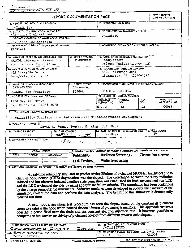
A Reliability Simulator 'or Radiation-Hard Microelectronics Development
Z.. _ SONAL AUTHORSMDavid H. Huang, Everett E. King, J.J. Wang
13a- -r.'P OF REPORT 13b. 7IME COVERED 14. OATE OV REPORT (Yea ,,,omnDay) 15. PAGI CCUNT
Final :koM9Dec01 " 91Apr30F 91,07,23 39
i. SUPPLEMENTARY NOTATION
CSAT COOFS :8. SUBJEC1T .TERMS (Canunm on r-wm ,f nftary an ,acnouy Cy odCa numo*iJ
Z;EO I ROUP I SU-ROUP Reliality, Radiation Screening, ChIannel hot-elecuon
LDD Devk=c-. Wafer level testing.
19. A43S -,AC 'Crnnue on rovwn it necemavy ana 4a&nfy by Woa~ wavoen
A real-time reliability simulator to predict device lifetime of n-chanmel MOSFET transistors due tochannel hot-electron (CHE) degradation was developed. The correlation between the x-ray radiationinduced and hot-electron induced interface state generation was established for both conventional non-LDDaad the LDD n-channel devices by using appropriate failure criteria. The correlation has been confirmedby the charge pumping measurements. Software modules were developed to control the hardware of thesimulator, collec;- the data and perform the data analysis. The benefit of this simulator is dramaticallyreduced test tie.
A new hot-carrier stress test procedure has been developed based on the constant gate current
stress to evaluate the hot-carrier induced device lifetime of p-channel transistors. This approach ensures a
constant electric field near the drain and the constant electron injection rate. It becomes possible tocompare the hot-carrier sensitivity of p-channel devices from different process technologies.
1. 'iST7Xf8JTON/AVALA8lLjtY OF AUs77AC7 !21. AB5TRAC SC.JRIT' CLASSIFICATION
11 uN..AS3IEDJNLMITSD = SAME AS P. '" : ' .;Sz. S UNCLkSStIFED
.2. 'JAME OF RESPONSIBLZ NOIVIOU.). 22b. TEL..E;?ONE fIJOU@* AI& CO*) I "2-" F;;C. SYMBOL
.erry Czerniak (703) 325-6626 D2001
IForm 1473, JUN 4 y.owazomo tv. -- ," ".aSSeF C,eCN OF ",IS 2AG-
LAS S I...D
A RELIABILITY SIMULATOR FOR
RADIATION-HARD MICROELECTRONICS DEVELOPMENT
Prepared by:
David H. HuangEverett E. KingJ.J. Wang
Advanced Research and Applications Corporation (ARACOR)425 Lakeside DriveSunnyvale, CA 94086
Contract No. DNA001-89-C-0194ARACOR Document FR793-91
July 1991
THIS WORK SPONSORED BY THE STRATEGIC DEFENSE INITIATIVE OFFICEAND MANAGED AND EXECUTED BY THE DEFENSE NUCLEAR AGENCY
TABLE OF CONTENTS
FOREWORD
EXECUTIVE SUMMARY
1.0 INTRODUCTION ...................................................................... 1
2.0 PROGRAM OVERVIEW ................................................................. 1
3.0 PHASE II WORK PLANS ................................................................ 2
3.1 Task 1 - PMOS Device Correlation ............................................. 2...
3.2 Task 2 - LDD Device Correlation ............................................... 33.3 Task 3 - Development of Reliability Simulator ................................ 3
3.4 Task 4 - Program Management and Reporting ................................ 3
4.0 CORRELATION RESULTS FOR N-CHANNEL LDD DEVICES ................. 3
4.1 Sample Description .................................................................. 3
4.2 Hot-Carrier Stress Test ......................................................... 4
4.3 Wafer-Level Radiation Test ................................................... 4
4.4. Correlation Model and Results ................................................. 5
5.0 POST-STRESS BEHAVIOR OF P-CHANNEL TRANSISTORS ............... 11
5.1 Sample Description and Test Procedure ...................................... 12
5.2 Conventional Constant Drain Voltage Stress ................................. 13
5.3 Constant Gate Current Stress .................................................... 16
6.0 SOFIWARE FOR THE SIMULATOR ............................................. 28 / -
7.0 PHASE II CONCLUSIONS .......................................................... 30
8.0 ACKNOWLEDGEMENT .............................................................. 31
9.0 REFERENCES ............................................................................. 31
&OO*Stion For
DTIC TABUnannounced C03
iustifioation
By
AD ft_r t but t on/Avatlabilitt uodos
LIST OF FIGURES
Figure
1 Schematic diagrams showing the two-section drain model, and its equivalent
circuit of LDD device structure ........................................................... 7
2 Lateral distribution of interface states near the drain end of the channel for
virgin device, devices after hot-carrier stress and X-ray irradiation. The
metallurgical drain junction is located at 1.0 .m .......................................... 8
3 Interface states generation as a function of total dose for the similar LDD device
as shown in Figure 2 ....................................................................... 9
4 The correlation between device lifetime, ,t-, and the figure-of-merit for
radiation-induced interface trapping, Deff ................................................. 10
5 Lateral distribution of interface states near the drain end of the channel for
virgin device, devices after hot-carria stress and X-ray irradiation. The
metallurgical drain junction is located at 1.0 p= ............................................. 11
6 AGm/Gm shift as a function of CHE stress time. Measured degradation Agm shows
the saturation ac stress time increase ...................................................... 14
7 Variations in impact-ionization substrate current and gate current during CHE stress.
The decrease indicates that fields in the silicon are decreasing during the stress ......... 15
8 The recorded gate and substrate currents as well as the drain voltage during
constant gate current hot-carrier stress for a typical p-channel device .................. 16
9 Isub, Ig, AVth, Agm/gm, and A5L/Id as function of stress gate voltage for a typical p-
M OSFET. Leff= .8 pm ......................................................................... 17
10 Threshold voltage shift as a function time for devices with different gate length ....... 18
11 Transconductance change as a function time for devices with different gate length .... 18
12 Drain current change as a function time for devices with different gate length ........... 19
ai
LIST OF FIGURES (continued)
13 Threshold voltage shift as a function time for different stress conditions on a device
w ith Lg=).7 ................................................................................ 19
14 Transconductance change as a function time for different stress conditions on a device
with Lg=0.7 t .............................................................................. 19
15 Drain current change as a function time for different stress conditions on a device
w ith Lg=0.7 Itm ................................................................................ 19
16 The change of the substrate current as a function of stress time during the constant
gate current stress for devices with different gate lengths .............................. 20
17 The comparison of the change substrate currents between constant Vd and Ig stresses
as a function of the stress time ............................................................ 21
18 (a).I.Ifetime versus gate current Ig for two different size p-channel devices.
(b).Lifetime versus substrate current Isub for two different size p-channel devices ..... 22
19 Device lifetime versus extrapolated substrate current at lifetime Isab(t=T) for p-channel
devices with different gate lengths ....................................................... 23
20 The definition of substrate current used in device lifetime correlation ................ 25
21 Device lifetime versus substrate current for different gate length of p-channel devices
obtained by constant gate current stress method ......................................... 26
22 Intercomparison of hot-carrier sensitivity of different technologies for p-channel
transistors using constant gate current stress experiments .............................. 26
23 Device lifetime defined by Agm/gmo versus substrate current for different gate lengths
of p-channel devices ........................................................................ 27
24 Device lifetime def:ied by AIj/Ido versus substrate current for different gate lengths of
p-channel devices ........................................................................... 27
, iii
FOREWORD
This Final Technical Report was prepared by Advanced Research and ApplicationsCorporation (ARACOR), Sunnyvale, CA, and documents the work performed under the directionof the Defense Nuclear Agency (Contract No. DNA001-89-C-0194, "A Reliability Simulator forRadiation-Hard Microelectronics Development"), for the period 1 December 1989 to 30 April1991. The technical monitor was Lt. Commander Lewis Cohn.
The Principal Investigator at ARACOR from the beginning through June, 1990 was Dr. L.J. Palkuti. From June of 1990 through the end of the program, the Principal Investigator was Dr.David Huang. From mid-September, 1990 through the end of the program, Everett King provided
guidance as the incoming manager of the Semiconductor Technologies Area at ARACOR. OtherARACOR personnel who participated in this program can be identified from the list of authors.
iv
EXECUTIVE SUMMARY
The objective of this program was to develop a real-time Reliability Simulator to predictdevice lifetime of submicron VLSI circuits due to channel hot-electron (CHE) degradation. Theapproach was to use an x-ray radiation stress to accelerate device damage instead of the usualelectrical stress. The benefit is reduced test time and a test that is more suitable for use at the waferlevel. The Reliability Simulator is now available for use by developers of radiation-hard VLSImicroelectronics and provides a means to perform a reliability screen on sub-micron CMOScircuits which is well-suited for production.
The correlation between channel hot-electron degradation and radiation-induced interfacetrapping in N-channel LDD devices has been established. The charge pumping measurement hasbeen performed to confirm such a correlation. It is demonstrated that a simple, fast X-ray radiation
test provides a useful means to predict the hot-carrier-induced device lifetime of both conventional
and LDD n-channel MOSFETs by using the appropriate failure criteria. In conventional n-MOSFETs, hot-carrier induced device lifetime, THE, is extrapolated at Isub/W= 5 pA/Wm by
defining failure criterion Agn./gmo=3% or A1&/Id0=3%, while HE for LDD devices is extrapolated
at Isub/W= 5 pA/lpm by defining failure criterion AVth=10 mV. Radiation figure-of-merit, Deff, isdefined as the total dose where the interface generation, ANit, is increased to the level of 5 x 101cm-2 . This is equivalent to transconductance degradation Agj/gm=0.5 in non-LDD devices. The
correlation procedure has been applied to seven different n-channel LDD devices and results show
strong evidence that the correlation has general application.
A new hot-carrier stress procedure has been developed to evaluate the hot-carrier induced
device lifetime of p-channel transistors. Unlike the conventional constant voltage stress, the gate
current is monitored and maintained constant during the stress by adjusting the drain stress voltage
at short time intervals. This approach ensures a constant electric field near the drain and a constant
electron injection rate. It eliminates the degradation saturation effect which usually occurs in the
conventional constant voltage stress test and which prevents one from accurately extrapolating the
device lifetime. A new lifetime extrapolation procedure has also be developed which makes itpossible to compare the hot-carrier sensitivity of different process technologies. Unfortunately, thecorrelation between x-ray irradiation and hot-carrier induced degradation in p-channel transistorswas not established in this program. Further study is needed to investigate the relationship of the
neutral hole trapping produced by X-ray irradiation and the neutral electron trapping produced by
hot-carrier stress.
v
The hardware of the simulator includes an HP-4145 semiconductor parametric tester andthe ARACOR Model 4100 x-ray irradiator. Software modules were developed to control thehardware of the simulator, collect and analyze the experimental data. The simulator is capable ofsimultaneously irradiating three devices to a total-dose of 20 Mrad(SiO2) in about 25 minutes, atwhich dose level the hot-carrier induced device lifetime can be extrapolated and correlated reliably.This measurement time is much shorter than the conventional electrical stress test which usuallytakes 50 minutes for each device.
vi
9I
1.0 INTRODUCTION
This document is submitted as the Final Report for research activities conducted under
DNA/SD[O Contract No.DNA001-89-C-0194, a Phase II Small Business Innovation Research
(SBIR) program. This report and the computer software package are the final deliverables of this
effort.
It is the purpose of this report to describe our correlation results for n-channel LDD devices
and a new lifetime prediction method for p-channel devices. The program overview is provided in
the next section, followed by the description of the original Phase II work plan. The correlation
experimental details including the devices utilized, the hot-carrier stressing and the wafer-level
radiation correlation procedure are presented in Section 4. In Section 5, the post-stress behavior of
the p-channel transistor are described and analyzed, and results of the constant gate current are
presented. The control, testing and data analysis software generated for the simulator are described
in Section 6. Our conclusions and suggestions for further work are given in Section 7.
2.0 PROGRAM OVERVIEW
The primary objective of this Phase I program was to develop a comprehensive wafer-level
radiation simulator for CHE-induced degradation and to demonstrate accurate predictions of CMOS
device lifetimes based on wafer-level x-ray irradiation test results. This procedure would allow theprediction of VLSI lifetime based on the measurement of substrate current and total-dose induced
interface-state generation rather than the long time electrical stressing technique.
There were three Phase II technical objectives. The first objective was to extend the
correlation data base for n-channel non-LDD devices between radiation tests and CHE reliabilit
achieved in Phase I to LDD n-channel devices. The second objective was to find correlation
between radiation tests and CHE reliability for p-channel devices. The final objective was to
develop the test procedures to extract CHE reliability predictions from wafer-level radiation
exposures.
The first objective outlined above was achieved by providing experimental evidence for a
direct correlation between hot-carrier degradation and radiation-induced iterface generation forvarious n-channel LDD devices. Although the correlation for p-channel devices was not
established, a new methodology to predict device lifetime for PMOS transistors has been
developed. Based on the initial results, this new lifetime extrapolation procedure allows one to
correlate PMOS devices of different sizes to a straight line, just as was the case for n-channel
1
devices. The result of meeting the third objective is the control, testing, and data analysis software
generated for the simulator. The software package to implement these procedures is available for
usL-,. The benefits obtained by this research are that a cost-effective method for monitoring hot-carrier device reliability is described for both conventional and LDD n-channel devices, and a newlifetime extrapolation method is demonstrated for p-channel devices.
3.0 PHASE II WORK PLANS
The Phase 1I program consisted of four technical tasks to be performed over a 20 monthstechnical effort period. The four technical tasks as outlined in the Phase II proposal were:
3.1 Task 1 - PMOS Device Correlation
To allow evaluation of CMOS device reliability, CHE degradation in PMOS devices will beevaluated in a manner similar to the tests performed in Phase I. The goals of task 1 are to providean extension of the data base between interface-trapping and CHE reliability to allow for theprediction of CMOS cirruit reliability.
It is our plan to correlate PMOS device lifetime with radiation hardness. For each processtype, NMOS and PMOS device stressing will be performed on a series of identical test transistorson the same wafer similar to the procedure developed in Phase I. In these experiments, theautomated wafer-probe system utilizing an HP Model 4145 parametric test system with suitablecontrol software will be utilized to provide evaluation of the device characteristics in both theforward and reverse mode. CHE stressing will be conducted over a period of I to 500 minutes.The CHE stress conditions will be selected based on the preliminary measurement of thenormalized substrate or gate currents, i.e. Ib/W and Ig/W.
The changes in the transistor characteristics such as maximum transconductance, Agm/gmo,
threshold voltage, AVr, and drain current, A40Lo, will be used to monitor device degradation.The device lifetime, tH, will be determined from these stress data.
Radiation-induced interface traps will be measured on fresh transistors on these samewafers by die-level exposures in an ARACOR Model 4100 X-ray Test System while the deviceswhich were biased at an oxide field of 0 or +2 MV/cm. Agn/gm and subthreshold slope ASw will
be utilized as the monitor of interface trapping.
2
3.2 Task 2 - LDD Device Correlation
The results in Phase I indicated that the correlation between CHE degradation and interface
trapping in LDD devices requires additional electrical measurements in addition to the substratecurrent to normalize geometric effects.
Since LDD devices are expected to become an important device design for advanced
CMOS, we will develop a correlation between CHE-lifetime of LDD devices with radiation-
induced trapping. LDD devices fabricated with different gate-oxide processes will be studied byCHE stress and radiation tests as outlined in the previous section and the results will be comparedwith similar results on non-LDD devices on the same wafer.
3.3 Task 3 - Development of Reliability Simulator
The CHE-stress results obtained for both conventional and LDD devices will be
incorporated into a reliability simulator based on a substrate current model to predict the lifetime in
test structures by radiation testing and substrate current measurements. The reliability simulator
will include test structures for both NMOS and PMOS device verification; test conditions and
procedures for wafer-level irradiation and device analysis software. It is the purpose of this task
to provide a prototype version of this reliability simulator for evaluation as a process development
tool.
3.4 Task 4 - Program Management and Reporting
In this task, the monitoring and reporting will be addressed. Project reports will be
provided on a quarterly basis summarizing the technical progress and financial issues. After the
completion of the program a final report describing the objectives, experimental details and
program results wil be provided.
4.0 CORRELATION RESULTS FOR N-CHANNEL LDD DEVICES
4.1 Sample Description
Measurements of hot-carrier and radiation-induced device degradation were made on n-
channel LDD test structures fabricated by five different venders utilizing various processes and
device geometries. These venders include AT&T, Honeywell, IBM, National Semiconductor and
Texas Instruments. The wafers incorporated standard-geometry test devices including both n- and
p-channel transistors. The effective channel lengths for the devices examined range from 0.4 to
3
1.5 microns with device widths ranging from 10 to 100 microns. The gate-oxide thicknesses
range from 150 to 250 A. Most of the devices were fabricated by n+ poly-Si gate and radiation
hardened processes.
4.2. Hot-Carrier Stress Test
For each device type examined in this project, hot-carrier stressing was performed on a
series of identical test structures on the same wafer. In these experiments, an automated wafer-probe system utilizing a Hewlett-Packard 4145 Semiconductor Parametric analyzer controlled by a
specially developed control software package was used to evaluate the device characteristics in both
the forward and reversed mode of operation. After initial device characterization, parametric testswere performed after each hot-carrier stress period. The typical stress period is 50 minutes and
device characteristics are monitored at 1, 2, 5, 10, 20 and 50 minutes. The devices were stressedat the worst-case degradation condition obtained at the gate voltage where the substrate current is
maximum (typically 3 V), while he drain stress voltage ranges from 5.0 - 8.0 V depending on thedevice gate length. The substrate is always biased at OV.
The changes in the transistor characteristics such as maximum transconductance, Agm/gmo,threshold voltage AVth, and drain current, A1d/Id0 in forward and reversed linear and saturationregions were used to monitor device degradation. The maximum gm and Vth were measured
utilizing the linear drain current versus gate voltage characteristics at drain voltage Vds=0.05 V,where gm is defined as the maximum slope and Vth the gate voltage at which the drain current
Ids--O. I WIL pA. W and L are the device width and gate length, respectively. In most cases, the
degradation in the forward-linear mode was used to determine device degradation, although, the
data for all four modes was recorded and evaluated.
4.3. Wafer-Level Radiation Test
Radiation-induced interface traps were measured on fresh transistors on those same wafers(described in Section 4.1) by wafer-level exposures in an ARACOR Model 4100 AutomaticSemiconductor Irradiation System while the devices were biased at gate voltage Vg= OV. In theseexperiments, the Model 4100 X-ray is combined with the HP 4145B described above. The pre-and post-irradiation device characterizations are monitored. The devices were exposed at doserates ranging from I to 10 x 105 rad(SiO2)/minutes to total dose level ranging from 1 x 10⁵ to 5 x10⁷ rad(SiO2). The typical final total dose level is 20 Mrad(SiO,) and device characteristics aremonitored after 100lK, 200K, 500K, 1M, 2M, 5M, 10M and 20 Mrad(SiO2).
4
Radiation-induced interface trap generation is monitored by the changes in the device's
subthreshold characteristics. It is found that the subthreshold slope technique is the only suitable
means to characterize interface state generation in n-channel LDD devices, while both subthreshold
slope and maximum gm are good monitors for non-LDD devices (the reason will be discussed in
the next sub-section). The changes in the transistor characteristics, such as subthreshold slope
ASw, threshold voltage AVth, and maximum transconductance, Agm/gm in forward linear and
saturation regions, were recorded and used to monitor device degradation.
4.4. Correlation Model and Results
The interface-state generation ANit serves as the link in the correlation between the radiation
and hot-carrier stress testing. In the short channel MOSFETs, electrons are strongly accelerated in
the electrical field near the drain and emitted into the gate oxide. This leads to interface-state
generation[ 1'2 ] which results in experimentally observed device degradation. On the other hand,
irradiation on devices causes both oxide charge trapping and interface-state generation in the gate
oxide. However, using the subthreshold slope measurement[31 allows one to extrapolate the
information of interface!-state generation. As a result, x-ray irradiation can be used as a prediction
tool to monitor the hot-carrier induced degradation in a relatively short test period. 1]
In order to correlate hot-carrier and radiation induced degradation, the hot-carrier lifetime,
tHE, and the total-dose figure-of-merit, Deff, have to be defined first. To define the hot-carrier
lifetime trH, the first step is to choose a failure criterion. For example, the saturation drain current
degradation Ald/Ido=3% is a commonly used criterion, which is equivalent to threshold voltage
shift AVth=10 mV for non-LDD devices.[5] An independent charge pumping study indicated that at
this failure criterion, approximately 5 x 1011 cm-2 interface states are generated.[61 The saturation
drain current degradation AId/Ij0=3% is also used as a failure criterion in the correlation for non-LDD devices. 4]
In the non-LDD device correlation, the figure-of-merit Deff, was defined as the total dose
where the maximum linear region transconductance degradation, Agmj/gm was reduced by 50%.
This is based on the fact tkiat the change of transconductance is linearly proportional to the change
of the interface density in the gate oxide.[7] It has been shown that the relationship between
transconductance and interface charge density can be expressed as follows:14,8]
Agm K x ANit (1)
5
where K 1 10-12 is a constant. Based on the above equation, the change of maximumtransconductance, Agm/gm, was used as a key parameter to monitor the change of interface traps
after X-ray irradiation in conventional non-LDD device correlation.
Based on the above discussion, the correlation between the hot-carrier and radiation
induced degradation is established at an interface-state generation of ANit=5 x 1011 cm-2 for non-
LDD devices. Ref[4] further developed the following model:
zI.ME=A' D1 -5(2)
where zt- is extrapolated at Isub/W=5 pA/Apm and A' is a constant. The above equation indicated
that oxides with low radiation-induced interface state generation are also insensitive to hot-carrier
induced degradation.
Series-Resistance in LDD Devices
In the LDD devices, however, there is another important degradation mechanism which
must be taken into account. Here, degradatiun can be caused by an increase in the channel series
resistance which is of quite a different nature than the transconductance and threshold voltage
degradations observed in conventional non-LDD devices. 9.10 The reason for this is that the LDD,
or spacer, region is only moderately doped and can be easily depleted by the hot-carrier-injection-
induced interface states which are generated. Similarly, if a LDD device is exposed to X-rayirradiation, both the radiation induced positive charge (ANot) and interface states (ANit) can easily
change the resistivities in the LDD spacer region. As shown in Figure 1, if such spacer region
extends outside the gate edge (as in the cases of low-dose LDD devices and/or devices with
insufficient gate to LDD region overlap), there will be no gate-controlled charge sheet formation in
the spacer region, and the resistivity of the LDD region can be changed dramatically. Therefore,
the source-drain series-resistance will also change dramatically.
On the other hand, it is well known that the extrinsic transconductance can be modeled as
follows:
gm(obs) = 1 gm (3)1+R' gm
where gm is the intrinsic transconductance and Rs the source-drain series resistance. The change in
Rs will influence the measurement of transconductance gm.
6
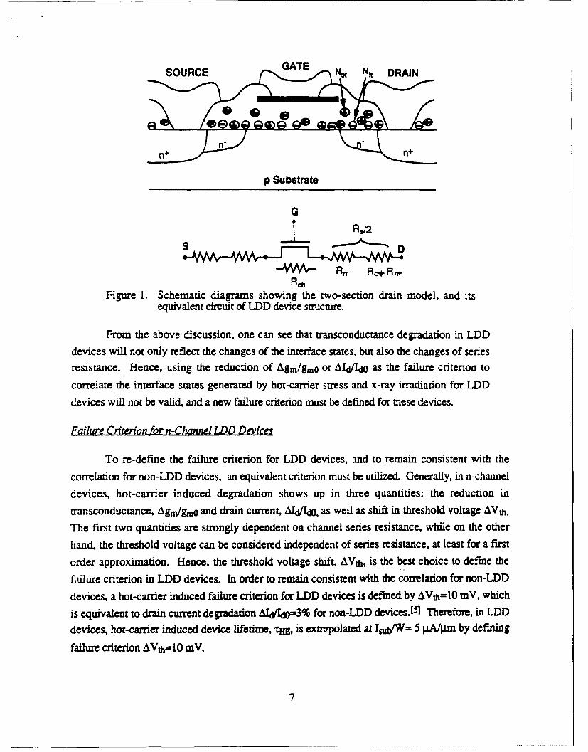
SOURCE GATE Not Nit DRAIN
n+ nn
p Substrate
G
J Rs/2
Rch
Figure 1. Schematic diagrams showing the two-section drain model, and itsequivalent circuit of LDD device structure.
From the above discussion, one can see that transconductance degradation in LDD
devices will not only reflect the changes of the interface states, but also the changes of series
resistance. Hence, using the reduction of Agm/gm0 or AId/Id0 as the failure criterion to
correlate the interface states generated by hot-carrier stress and x-ray irradiation for LDD
devices will not be valid, and a new failure criterion must be defined for these devices.
Failure Criterion for n-Channel LDD Devices
To re-define the failure criterion for LDD devices, and to remain consistent with the
correlation for non-LDD devices, an equivalent criterion must be utilized. Generally, in n-channel
devices, hot-carrier induced degradation shows up in three quantities: the reduction in
transconductance, Agw/go and drain current, AIdJId0, as well as shift in threshold voltage AVth.
The first two quantities are strongly dependent on channel series resistance, while on the other
hand, the threshold voltage can be considered independent of series resistance, at least for a first
order approximation. Hence, the threshold voltage shift, AVth, is the best choice to define the
ftilure criterion in LDD devices. In order to remain consistent with the correlation for non-LDD
devices, a hot-carrier induced failure criterion for LDD devices is defined by AVth=10 mV, which
is equivalent to drain current degradation ALj(dL=3% for non-LDD devices.[51 Therefore, in LDD
devices, hot-carrier induced device Lifetime, ',r, is extrapolated at Isub/W= 5 j.±/znA by defining
failure criterion AVthfl0 mV.
7
On the other hand, due to the effect of series resistance, transconductance degradation,
Agmlgm, will no longer be a valid indicator of interface-states generated for LDD devices in the
radiation test. Similarly, in order to remain consistent with the correlation for non-LDD devices, a
radiation induced failure criterion for LDD devices is defined by ANit= 5 x 1011 cm -2 , which isequivalent to transconductance degradation Agm/gm= 50 % for non-LDD devices. 4 Therefore, in
LDD devices, the radiation figure-of-merit, Deff, is defined as the total dose where the interface
generation, ANit is increased to the level of 5 x 1011 cm-2.
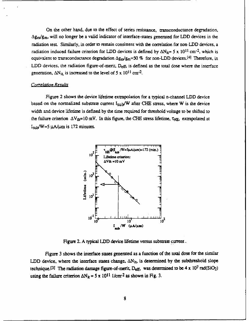
Correkaton Results
Figure 2 shows the device lifetime extrapolation for a typical n-channel LDD devicebased on the normalized substrate current Isub/W after CHE stress, where W is the device
width and device lifetime is defined by the time required for threshold voltage to be shifted to
the failure criterion AVth-10 inV. In this figure, the CHE stress lifetime, tHE, extrapolated at
Isub/W=5 pA/p.m is 172 minutes.
10, rI4E@(j* /w=5 /A1 )= 17 (n.)Lifetime iterion:
d, 10
sb 1W (A/A4m)
Figure 2. A typical LDD device lifetime versus substrate current.
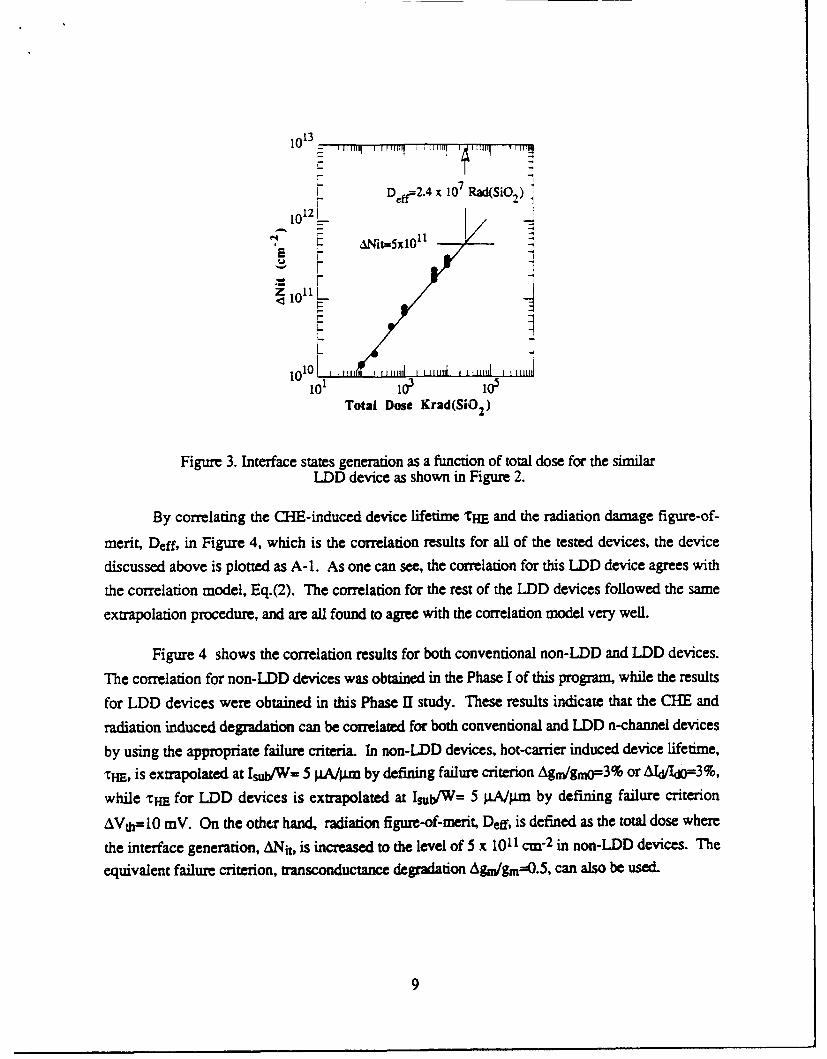
Figure 3 shows the interface states generated as a function of the total dose for the similar
LDD device, where the interface states change, ANit, is determined by the subthreshold slope
technique.[3] The radiation damage figure-of-merit, Deft, was determined to be 4 x 10⁷ rad(SiO2)
using the failure criterion ANit = 5 x 10¹¹ I/CM 2 as shown in Fig. 3.
8
113
- Dff=2.4 x 10⁷ Rad(SiO 2 )
1012
'2 ANitf5x101
L I
L
1010
Total Dose Krad(SiO2 )
Figure 3. Interface states generation as a function of total dose for the similarLDD device as shown in Figure 2.
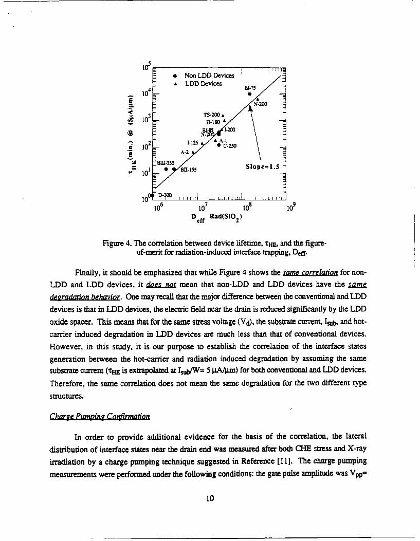
By correlating the CHE-induced device lifetime THE and the radiation damage figure-of-
merit, Deff, in Figure 4, which is the correlation results for all of the tested devices, the device
discussed above is plotted as A-1. As one can see, the correlation for this LDD device agrees with
the correlation model, Eq.(2). The correlation for the rest of the LDD devices followed the same
extrapolation procedure, and are all found to agree with the correlation model very well.
Figure 4 shows the correlation results for both conventional non-LDD and LDD devices.
The correlation for non-LDD devices was obtained in the Phase I of this program, while the results
for LDD devices were obtained in this Phase II study. These results indicate that the CHE and
radiation induced degradation can be correlated for both conventional and LDD n-channel devices
by using the appropriate failure criteria. In non-LDD devices, hot-carrier induced device lifetime,
THE, is extrapolated at IsubW= 5 jIA/pm by defining failure criterion Agm/gmo= 3 % or AI&/1d 3%,
while rHE for LDD devices is extrapolated at Isub/W= 5 p.A/pm by defining failure criterion
AVth=10 mV. On the other hand, radiation figure-of-merit, Deff, is defined as the total dose where
the interface generation, ANit, is increased to the level of 5 x 10¹¹ cn "2 in non-LDD devices. The
equivalent failure criterion, transconductance degradation Agm/gm=0.5, can also be used.
9
0 Non LDD Devices£ LDD Devices
104 _17
N4-200
3 TS-200-i' 10- H-18o
1-3J0._ 102 '-125£ U-
S -- A-2a "BIB-355
SU i-55 Slope=l.101 3II-155
106 107 10a 109
D Rad(SiO )eff 2
Figure 4. The correlation between device lifetime, rHE, and the figure-of-merit for radiation-induced interface trapping, Deff.
Finally, it should be emphasized that while Figure 4 shows the same correlation for non-
LDD and LDD devices, it does no mean that non-LDD and LDD devices have the same
degradation behavior. One may recall that the major difference between the conventional and LDD
devices is that in LDD devices, the electric field near the drain is reduced significantly by the LDD
oxide spacer. This means that for the same stress voltage (Vd), the substrate cirrent, Isub, and hot-
carrier induced degradation in LDD devices are much less than that of conventional devices.
However, in this study, it is our purpose to establish the correlation of the interface states
generation between the hot-carrier and radiation induced degradation by assuming the same
substrate current (rHE is extrapolated at Isub/W= 5 p Am) for both conventional and LDD devices.
Therefore, the same correlation does not mean the same degradation for the two different type
structures.
Chare PM aing Coirmtion
In order to provide additional evidence for the basis of the correlation, the lateral
distribution of interface states near the drain end was measured after both CHE stress and X-ray
irradiation by a charge pumping technique suggested in Reference [I1]. The charge pumping
measurements were performed under the following conditions: the gate pulse amplitude was Vpp=
10
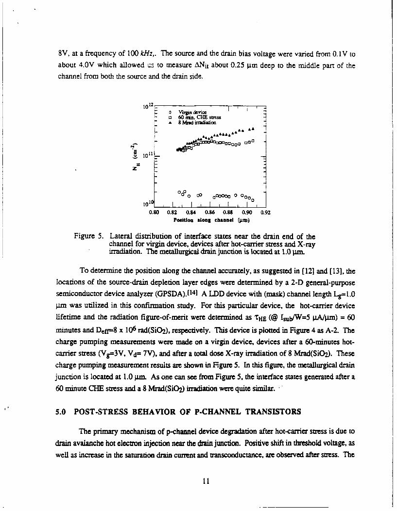
8V, at a frequency of 100 kHz,. The source and the drain bias voltage were varied from 0.1V toabout 4.OV which allowed us to measure ANit about 0.25 j.±m deep to the middle part of the
channel from both the source and the drain side.
o 60 un. CHE sumaA6 8 MNd kachioa
A& A&AIA'& "L A
A mac13 loa -3
1011A
101 2 00000 0 01 0[0 1 I I I I I I I I I I
0.80 0.82 0.84 0.86 0.88 0.90 0.92Position along channel (gim)
Figure 5. Lateral distribution of interface states near the drain end of thechannel for virgin device, devices after hot-carrier stress and X-rayirradiation. The metallurgical drain junction is located at 1.0 pm
To determine the position along the channel accurately, as suggested in [12] and [13], the
locations of the source-drain depletion layer edges were determined by a 2-D general-purpose
semiconductor device analyzer (GPSDA).[ 141 A LDD device with (mask) channel length Lg= l.0pm was utilized in this confirmation study. For this particular device, the hot-carrier device
lifetime and the radiation figure-of-merit were determined as THE (@ Isub/W=5 pA/Wm) = 60
minutes and Deff=8 x 10⁶ rad(SiO2), respectively. This device is plotted in Figure 4 as A-2. The
charge pumping measurements were made on a virgin device, devices after a 60-minutes hot-
carrier stress (Vg= 3 V, Vd= 7V), and after a total dose X-ray irradiation of 8 Mrad(SiO2). These
charge pumping measurement results are shown in Figure 5. In this figure, the metallurgical drainjunction is located at 1.0 gm. As one can see from Figure 5, the interface states generated after a
60 minute CHE stress and a 8 Mrad(SiO2) irradiation were quite similar. -
5.0 POST-STRESS BEHAVIOR OF P-CHANNEL TRANSISTORS
The primary mechanism of p-channel device degradation after hot-carrier stress is due to
drain avalanche hot electron injection near the drain junction. Positive shift in threshold voltage, aswell as increase in the saturation drain current and transconductance, are observed after stress. The
11
positive threshold shift is indicative of the negative trapped charges in the gaze oxide. This is also
supported by the fact that the subthreshold slope almost remained constant before and after stress.
The hot-carrier mechanism is due to the high electric field near the drain junction which acceleratesthe carriers and generates electron-hole pairs through impact ionization. The resulting electrons are
accelerated toward the gate where a portion become trapped in the gate oxide.
On the other hand, during X-ray irradiation, oxide and interface trap charges induced in theSiO 2 layer are both positive. Unlike the case for n-channel device correlation, in which the
interface state generation serves as the link between hot-carrier and X-ray radiation induced
degradation, there is no such obvious link in the case of the p-channel transistors. There is,
however, a suggestion that the correlation might be established based on the neutral hole traps
produced by X-ray irradiation and the neutral electron traps produced by hot carrier stress. In
order to establish such a correlation, the behavior of electron traps after hot-carrier stress must be
investigated more carefully. In this Phase I program, however, the focus was on the device
behavior after hot electrons are injected into gate oxide. A new stress procedure was proposed andapplied, and the results of this new stress procedure are superior to the conventional stress
procedure.
Whereas a general agreement exists on lifetime criteria for NMOS transistors (e.g., 10 mV
of threshold voltage, Vth, shift or 10% decrease of transconductance, gm), many methodologies
can be found in the literature for lifetime evaluation of PMOS transistors. Some authors havereported a correlation with substrate current 'ub,[15,161 gate current Ig,( 17] or both parameters.[ 181
Others[ 191 have proposed to stress transistors at constant substrate and drain current in order to
compare the hot carrier sensitivity of different technologies. This lack of uniformity comes from
specific difficulties of PMOS aging characterization.
5.1 Sample Description and Test Procedure
Measurements of hot-carrier degradation were made on wafers fabricated by IBM and
Honeywell. The wafers incorporated standard-geometry test devices including both n- and p-channel transistors. The effective channel lengths for the devices examined ranged from 0.5 to 1.5microns with device widths ranging trom 10 to 50 microns. The gate-oxide thicknesses are 175and 200 A, respectively. The devices were fabricated with an n+ poly-Si gate (i.e., buried channelPMOS) process.
For each device type examined, hot-carrier stressing was performed on a series of identicaltest structures on the wafer. In these experiments, the automated wafer-probe system (described
12
in section 4.2) was used to evaluate the device characteristics in both the forward and reversed
mode of operation. After initial device characterization, parametric tests were performed after eachhot-carrier stress period. The hot-carrier stress period ranged from 50 to 1000 minutes and device
characteristics were typically monitored at 1, 2, 5, 10, 20, and 50 minutes. The devices werestressed at the worst-case degradation condition obtained at the gate voltage (typically -1 - -2V),where the gate current rather than the substrate current reached a maximum while the stressed drain
voltage ranged from -5 - -8 V depending on device gate length. The substrate was always biased
at OV.
The changes in the transistor characteristics, such as threshold voltage AVth, maximum
transconductance, Agm/gmo, and drain current, Ald/Ido, in forward and reversed linear and
saturation regions, were used to monitor device degradation. The maximum gm and Vth were
measured utilizing the linear drain current versus gate voltage characteristics at drain voltage Vds= -0.05 V, where gm is defined as the maximum slope and Vth the gate voltage as such that the draincurrent Ids= -0.1 W/L LA, W and L are the device width and gate length, respectively. In most
cases, the degradation in the forward-linear mode was used to determine device degradation,although, the data for all four modes was recorded and evaluated.
5.2 Conventional Constant Drain Voltage Stress
During the conventional hot-carrier stress experiment, a p-channel transistor is biased at
fixed drain, gate, source, and substrate voltage all the time. If the hot-carrier stress damage for p-
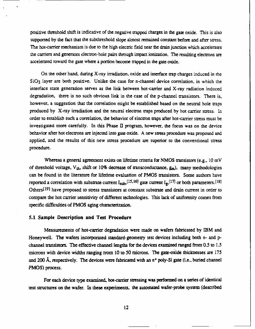
channel devices is examined as a function of stress time, it is found that the degradation change(such as AVth, Agm/gmo, or AIL/d0) as a function of time does not follow a power law, as in thecase of n-channel devices, but rather shows a decreasing gradient as the stress time increases, asshown in Figure 6. As a result of this non-linearity, power law extrapolation of the curve andextraction of the lifetime is hazardous and unreliable. A meaningful lifetime, 'r, versus the
substrate current I,b relationship can no longer be obtained and a comparison of the hot-carriersensitivity of different technologies becomes impossible.
13
10,e AGm Measured Dam (Lg=1 .0m)
[ Dash Line: Curve fiting by:I 1.1 31( +.14. 99)
- Solid Line: Power law fitting
I L
l0 101 1o2 103 leCHE Stress Time (min.)
Figure 6. AGn/Gm shift as a function of CHE stress time. Measureddegradation Agm shows the saturation as stress rime increase.
There are two explanations for this saturation behavior. (1) the trapped charge in the oxide
influences the field in the silicon, decreasing the lateral field and lowering the impact ionization
substrate current. The gate current, similarly, decreases with stress time; (2) a recent paper[20]
suggested that this decreasing gradient behavior follows the growth of the electron trapped region
from drain to source while assuming the lateral field is completely unaltered. It is our belief that
both mechanisms are involved in the p-channel device degradation process.
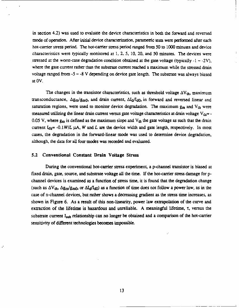
If the substrate current or the gate current is monitored as a function of constant voltage
stress time, it is found that both substrate and gate current decrease during the stress, as shown in
Figure 7. These decreases are due to the trapped charge in the oxide. The trapped chargeinfluences the field in the silicon, decreasing the lateral field and lowering the impact ionization
substrate current. Figure 7 shows that gate current decreases as much as a factor of 10 during 500
minutes of stress, while the substrate current decreases as much as a factor of 2. The device gate
lengths range from 0.5 to 1.0 pm.
It is obvious that the saturation of the degradation parameter is caused be electron trappingduring constant voltage stress. Indeed, trapped electrons reduce the lateral electric field in the
14
103 ... ........ 101
L -0.5--.0
g 10M0
1 CtI-_
1 0 1 - 1 0 - I
Solid Lines: I Dash Lines: I
V =-1.0 V; Vd=-. 5 V
oo I . I - -I , 10-2l o 101 to2 to
CHE StressTime (min.)
Figure 7 The variations in the impact-ionization substrate current and gatecurrent during CHE stress. The decrease indicates that fields inthe silicon are decreasing during the stress.
channel and induce a transversal electric field in the oxide that repels further injection. A constant
drain and substrate current stress was proposed earlier 19l, in which the p-channel device is
stressed by imposing constant drain and substrate current, while keeping the source and gate
voltages constant. Thus, the drain and substrate voltages must be varied during the stress period.
This ensures a constant impact ionization rate, which should guarantee a constant electron injection
current, greatly suppressing the saturation effect. However, an accurate device lifetime prediction
cannot still be obtained by such constant drain/substrate currents stress.(191
In p-channel devices, it has been shown that the maximum damage condition corresponds
to the maximum substrate current. This behavior is in contrast with the n-MOS devices, where
maximum damage occurs at the maximum gate current. The correlation of maximum damage to the
maximum gate current supports the model in which it is the injected electrons that are responsible
for the traps. A recent simulation study 20 shows that the degradation parameter saturation effects
originated from the logarithmic growth of a region of filled traps from the drain junction towards
the source. In this model, the decrease of the gate current during the hot-carrier stress period was
explained by the assumption that the traps are gradually saturated in the injected region as stress
time increases, but the decrease in the substrate current is not explained if the lateral electric field is
15
completely unaltered, as claimed in the model. However, the most important conclusion of this
study is that gate current is a very useful indicator for hot-carrier induced degradation in P-channel
devices.
5.3 Constant Gate Current Stress
Stress Procedure
In the constant gate current stress method we proposed here, the gate voltage (typically, -I- -2 V) is consistently biased such that maximum gate current is obtained (i.e., the device is always
biased in the worst-case degradation condition). The gate current was monitored at short intervals
of time (e.g., 15 seconds), and kept constant to maintain constant electron injection rate duringstress by adjusting the drain voltage Vd under computer control. Besides monitoring the gate
current, the time dependency of the substrate current and the adjusted drain voltage were also
recorded at the same time during stress.
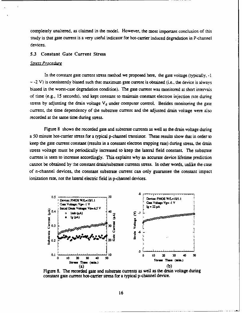
Figure 8 shows the recorded gate and substrate currents as well as the drain voltage during
a 50 minute hot-carrier stress for a typical p-channel transistor. These results show that in order to
keep the gate current constant (results in a constant electron trapping rate) during stress, the drainstress voltage must be periodically increased to keep the lateral field constant. The substrate
current is seen to increase accordingly. This explains why an accurate device lifetime prediction
cannot be obtained by the constant drain/substrate currents stress. In other words, unlike the case
of n-channel devices, the constant substrate current can only guarantee the constant impactionization rate, not the lateral electric field in p-channel devices.
0.5 50 r 1b.
Device: PMOS WjL=IW. I Device: P vM W/E--O/1.1GemVolage:Vp-1 V fA VltpA -
10. - 2pIrmua DnM Vdu w Vd=..5 V
0 .4 . . .( . ...
0.1I '. .. I. . 'I . . . .t. . 10 0 10 20 30 40 500 . 0 20 30 40 - StuilTe(m3i.)
(a)()Figure 8. The recorded gate and substrate currents as well as the drain voltage duringconstant gaze current hoC-carrier stress for a typical p-channel device.
16
Correlation of Device Degradation with Substrate and Gate Currents
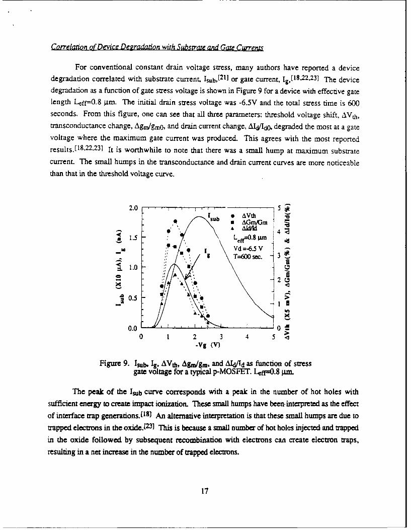
For conventional constant drain voltage stress, many authors have reported a devicedegradation correlated with substrate current, Isub,[ 2 1l or gate current, Ig,[18 ,2 2 ,2 3l The devicedegradation as a function of gate stress voltage is shown in Figure 9 for a device with effective gatelength Leff=0.8 gm. The initial drain stress voltage was -6.5V and the total stress time is 600seconds. From this figure, one can see that all three parameters: threshold voltage shift, AVth,transconductance change, Ag/gmo, and drain current change, AIAjI0, degraded the most at a gatevoltage where the maximum gate current was produced. This agrees with the most reported
results.[(18 ,22,231 It is worthwhile to note that there was a small hump at maximum substratecurrent. The small humps in the transconductance and drain current curves are more noticeable
than that in the threshold voltage curve.
2.0 I5Isub AVth,•, n AGm/Gm ;
1.5 Laff=0. 8un .4.. Vd =-6.5 V
T=600 sec.
=L 1.0 :
0.5 >
0.0------ 00 1 2 3 4 5
.Vg (v)
Figure 9. Isub, Ig, AVth, Agm/gm, and AId/Td as function of stressgate voltage for a typical p-MOSFET. Leff=0.8 im.
The peak of the Isub curve corresponds with a peak in the number of hot holes withsufficient energy to create impact ionization. These small humps have been- interpreted as the effectof interface trap generations.( 18] An alternative interpretation is that these small humps are due totrapped electrons in the oxide.[231 This is because a small number of hot holes injected and trappedin the oxide followed by subsequent recombination with electrons can create electron traps,
resulting in a net increase in the number of trapped electrons.
17
Evolution of Degradation with Stress Time
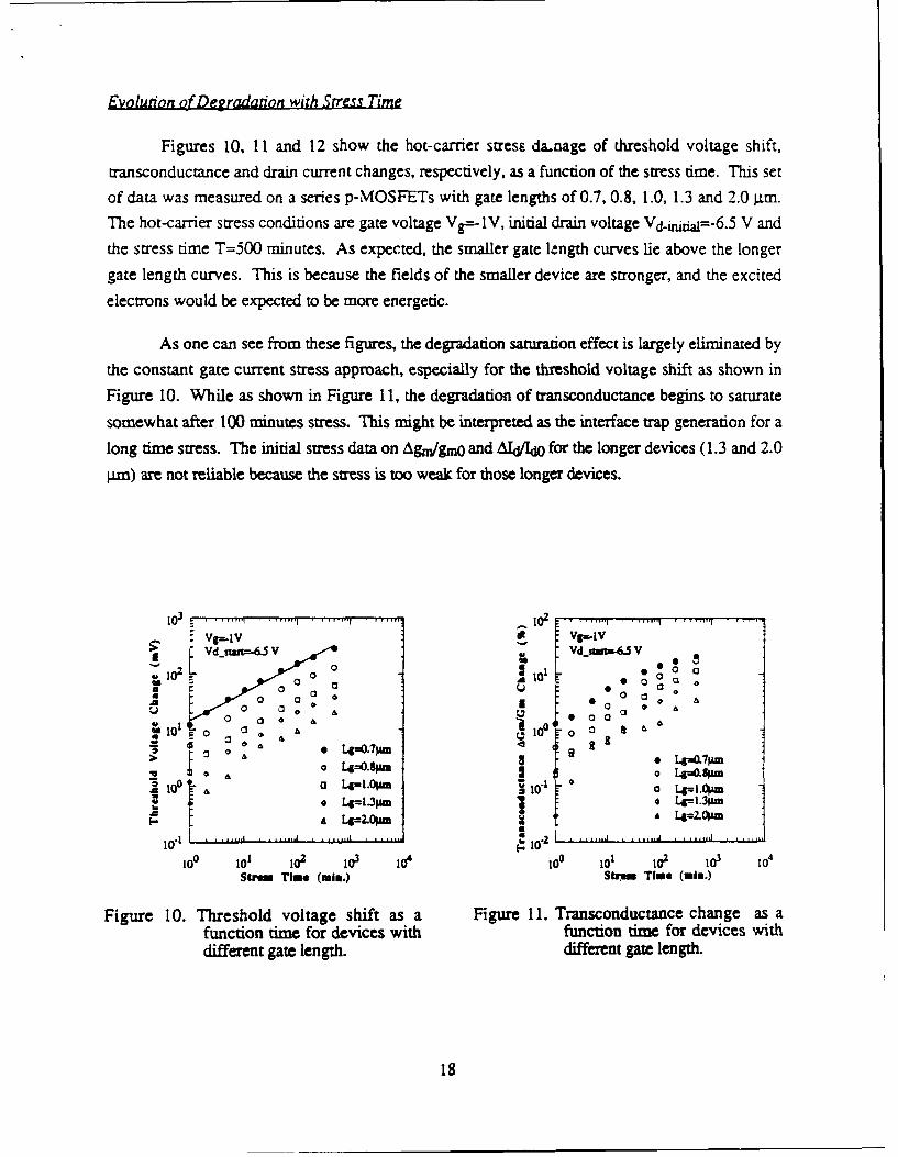
Figures 10, 11 and 12 show the hot-carrier stress danage of threshold voltage shift,
transconductance and drain current changes, respectively, as a function of the stress time. This set
of data was measured on a series p-MOSFETs with gate lengths of 0.7, 0.8, 1.0, 1.3 and 2.0 g±m.
The hot-carrier stress conditions are gate voltage Vg=- 1V, initial drain voltage Vd.jnitia=-6.5 V and
the stress time T=500 minutes. As expected, the smaller gate leangth curves lie above the longer
gate length curves. This is because the fields of the smaller device are stronger, and the excited
electrons would be expected to be more energetic.
As one can see from these figures, the degradation saturation effect is largely eliminated by
the constant gate current stress approach, especially for the threshold voltage shift as shown in
Figure 10. While as shown in Figure 11, the degradation of transconductance begins to saturate
somewhat after 100 minutes stress. This might be interpreted as the interface trap generation for a
long time stress. The initial stress data on Agn/gmo and AIdJld0 for the longer devices (1.3 and 2.0
pm) are not reliable because the stress is too weak for those longer devices.
dstazt-6v V vd~.6SV- , , , - I I I11 11 12Vd_s =-, V v4 • o a5
al 2 : * oa aUo L
000 o 0 * & &'3 a 0.4-- 1 100, 0 L 0-i N
A 6 LA . H
A 0 t40.12 lop o 10 01.. i 1.=3~ 1 ,) 14=.3M m"I °I- £ [4=2.oth A Ir=-AoA1D
10. . .. ...__ _ _ _ _ ...__ _ .. ..__ _.. .._ _1__ _.. .. , ...... J . . .., . ..
10° 10'2o io3 lo 100 io i02 l 1
Stre,, Tim* (ml.) Strin Time (mir.)
Figure 10. Threshold voltage shift as a Figure 11. Transconductance change as afunction time for devices with function time for devices withdifferent gate length. different gate length.
18
io2 ~ 3,
01
0
0 :3 A
e Lg=. 7Mim8 L'.ji > 10~ Initial Drain VoltageI
ag14i e Vd=-7.0* *L=lJpm nU Vd.67
.~~ oVdz6.5102 '10
to00 101 l 10 3 0 o 100Stress Time (mim.) lp1 0
Str. Time (Wit.)
Figure 12. Drain current change as a Figure 13. Threshold voltage shift as afunction time for devices with function time for different stressdifferent gate length. condition on a device with
Lg-O.7 jm
Vg--.1 V=0. L&07 u
S10 0 bnind Dram Voltage -1
a V ~ z 47 o V=0a~ VV.a7 U
e~da Vd6J :10t- 0
SrnTime (min.) Sir=e Time (aim.)
Figure 14. Transconductance change as a Figure 15. Drain current change as afunction time for different stress function-time for different stressconditions on a device with conditions on a device withLg-0.7 pim. L9=0.7 pm.
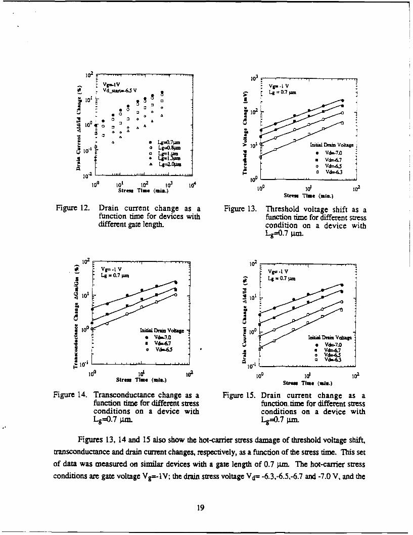
Figures 13, 14 and 15 also show the hot-carrer stress damage of threshold voltage shift,transconductance and drain current changes, respectively, as a function of the stress rime. This setof data was measured on similar devices with a gate length of 0.7 pm The hot-carrier stressconditions are gate voltage Vg=-lV; the drain stress voltage Vd= -6.36.5-6.7 and -7.0 V, and the
19
stress time T=50 minutes. As one can see from these figures, the degradation saturation effect is
eliminated by the constant gate current stress approach. As expected, the high stress voltagecurves lie above the lower stress voltage curves. This is because the fields at high stress voltages
are stronger, and the excited electrons would be expected to be more energetic.
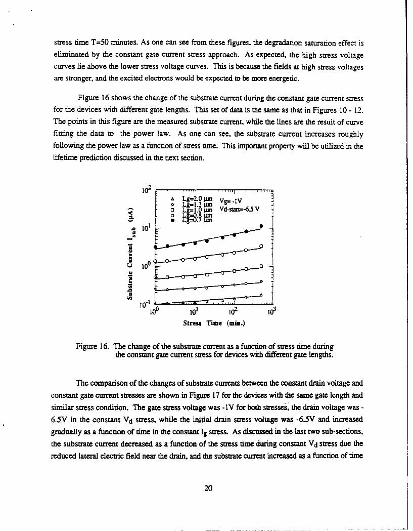
Figure 16 shows the change of the substrate current during the constant gate current stress
for the devices with different gate lengths. This set of dam is the same as that in Figures 10 - 12.The points in this figure are the measured substrate current, while the lines are the result of curve
fitting the data to the power law. As one can see, the substrate current increases roughly
following the power law as a function of stress time. This important property will be utilized in thelifetime prediction discussed in the next section.
10 , , , , - ,I
I I I . - t [
12 Lg=2.0 im Vg=.lV
o g= .-1 Vd-s mar-6.5 V
I--
- 100
10- .. ....... . ............. .....
10&1
100 101 102 101
Stress Time (min.)
Figure 16. The change of the substrate current as a function of stress time duringthe constant gate current stress for devices with different gate lengths.
The comparison of the changes of substrate currents between the constant drain voltage and
constant gate current stresses are shown in Figure 17 for the devices with the same gate length and
similar stress condition. The gate stress voltage was -IV for both stresses, the drain voltage was -6.5V in the constant Vd stress, while the initial drain stress voltage was -6.5V and increasedgradually as a function of time in the constant Ig stress. As discussed in the last two sub-sections,
the substrate current decreased as a function of the stress time during constant Vd stress due the
reduced lateral electric field near the drain, and the substrate current increased as a function of time
20
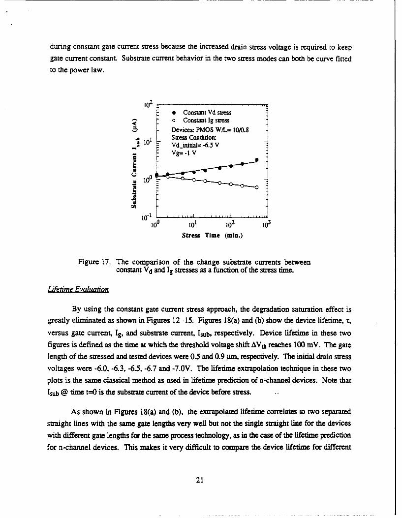
during constant gate current stress because the increased drain stress voltage is required to keepgate current constant. Substrate current behavior in the two stress modes can both be curve fittedto the power law.
102:r ....
e Constant Vd suesso Constant Ig swess
-, r- Devices: PMOS W/L= 10/0.8to Stres Condition:
Vd-inidal= -6.5 VVg=-1 V
I.. L
10& 3 o
10 , . . . . .2.. .. .I , . . .
100 101 102 10oStress Time (min.)
Figure 17. The comparison of the change substrate currents betweenconstant Vd and Ig stresses as a function of the stress time.
Lifetime Evaluation
By using the constant gate current stress approach, the degradation saturation effect isgreatly eliminated as shown in Figures 12 -15. Figures 18(a) and (b) show the device lifetime, r,
versus gate current, Ig, and substrate current, Isub, respectively. Device lifetime in these two
figures is defined as the time at which the threshold voltage shift AVth reaches 100 mV. The gatelength of the stressed and tested devices were 0.5 and 0.9 gm, respectively. The initial drain stress
voltages were -6.0, -6.3, -6.5, -6.7 and -7.OV. The lifetime extrapolation technique in these two
plots is the same classical method as used in lifetime prediction of n-channel devices. Note that
Isub @ time t=O is the substrate current of the device before stress.
As shown in Figures 18(a) and (b), the extrapolated lifetime correlates to two separated
straight lines with the same gate lengths very well but not the single straight line for the deviceswith different gate lengths for the same process technology, as in the case of the lifetime prediction
for n-channel devices. This makes it very difficult to compare the device lifetime for different
21
process technologies. The slope in the gate current correlation is about -1.0 and for substratecurrent correlation about -2.0.
o0.5im o 0.5JAn L' * 0.9 * 0.9 PM
r. io-
0
=.0.0--70OV
101, - Vdi=IOOmV 101L ,VdtlOOmV i
Vg=. 1.5 V !Vg=. ' .S V
Vdt_ =-6.0 - -7.0 V Vd =-6.0 - -7.0V ilo ... ... . ... "I ,.. ... lop . . .... . .. ..,
10 "1 1o0 101 1o1 io2 lo" 100
I1/W (pAilgm) Tsub(t=O)lW (lA/jm)
Figure 18(a). Lifetime versus gate current Ig Figure 18(b). Lifetime versus substrate currentfor two different size of p- Isub for two different size of p-channel devices, channel devices.
It is our goal to find a general lifetime prediction approach for p-channel devices, whichwill make it possible to compare the hot-carrier sensitivity of different technologies. To
accomplish this, the standard classical lifetime extrapolation to predict p-channel device lifetime
must be modified. In our new lifetime extrapolation approach, instead of using Isub(t=O), the
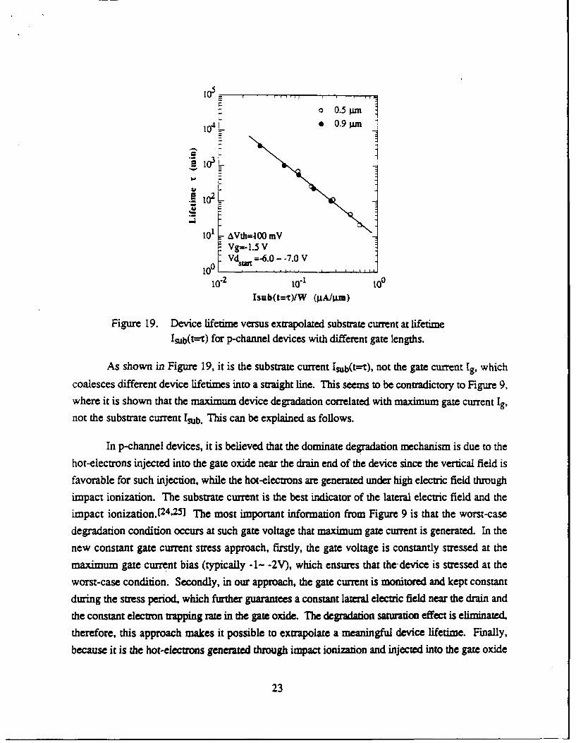
substrate current extrapolated, by power law (see Figures 16 and 17), at lifetime (i.e., Isub(t--'t))
was used as a degradation monitor. Figure 19 shows this new lifetime extrapolation approach.
The data set shown in Figure 19 is the same set of data shown in Figure 18(a) and (b). The only
difference is that in Figure 19, Isub(t= ) was used, while Isub(t=O) was used in Figure 18(b). As
one can see in Figure 19, the extrapolated device lifetime correlated to a single straight 'ine for the
devices with different gate lengths, as in the case of n-channel devices. The correlation can be
expressed as 'Isub- n with n=1.8.
22
7-- o 0 .5 p z m
" 0.9.im
: 1 L.~io
2 L
101 AVzh=IO0 mV
Vg=-1.5 V
10 i Vstm =-6.0 - -7.0 V
i0 -2 1 0- i00
Isub(t=,r)/W (IIA/ltm)
Figure 19. Device lifetime versus extrapolated substrate current at lifetime
Isub(t--r) for p-channel devices with different gate lengths.
As shown in Figure 19, it is the substrate current Isub(t--T), not the gate current Ig, which
coalesces different device lifetimes into a straight line. This seems to be contradictory to Figure 9,where it is shown that the maximum device degradation correlated with maximum gate current Ig,
not the substrate current Isub. This can be explained as follows.
In p-channel devices, it is believed that the dominate degradation mechanism is due to the
hot-electrons injected into the gate oxide near the drain end of the device since the vertical field is
favorable for such injection, while the hot-electrons are generated under high electric field through
impact ionization. The substrate current is the best indicator of the lateral electric field and the
impact ionization.(24 ,2-5 The most important information from Figure 9 is that the worst-case
degradation condition occurs at such gate voltage that maximum gate current is generated. In the
new constant gate current stress approach, firstly, the gate voltage is constantly stressed at the
maximum gate current bias (typically -1- -2V), which ensures that the-device is stressed at the
worst-case condition. Secondly, in our approach, the gate current is monitored and kept constant
during the stress period, which further guarantees a constant lateral electric field near the drain and
the constant electron trapping rate in the gate oxide. The degradation saturation effect is eliminated,therefore, this approach makes it possible to extrapolate a meaningful device lifetime. Finally,because it is the hot-electrons generated through impact ionization and injected into the gate oxide
23
which induce the device performance degradation, the correlation of device lifetime with different
gate lengths can be achieved by the substrate current Isub, instead of the gate current Ig.
In the correlation shown in Figure 19, unlike the case for n-channel devices, the substratecurrent extrapolated to the lifetime, Isub(t--), was used. The reason for this is that in p-channel
device stress experiments, the substrate current changes significantly due to the tapped hot-
electron in the gate oxide which, therefore, alter the lateral electric field distribution, while in n-
channel stress experiments, the change of the substrate current is relatively much smaller. For
example, when an n-channel device with W/L=0/l.0 pm/pm was stressed at Vd-6.5 V for a 50-minute period, the change of the substrate current, AIsub/Isubo was only about +3%, while on the
other hand, when a p-channel device with the same geometric parameters was stressed at Vd=-6.5
V for the same period, the changes of the substrate current, AIsubIsubo were -41% and +38% for
constant drain voltage and constant gate current stress, respectively. Due to the dramatic change of
the substrate current in stress experiments for p-channel devices, a correlation of the device lifetime
must be established based on the same assumption.
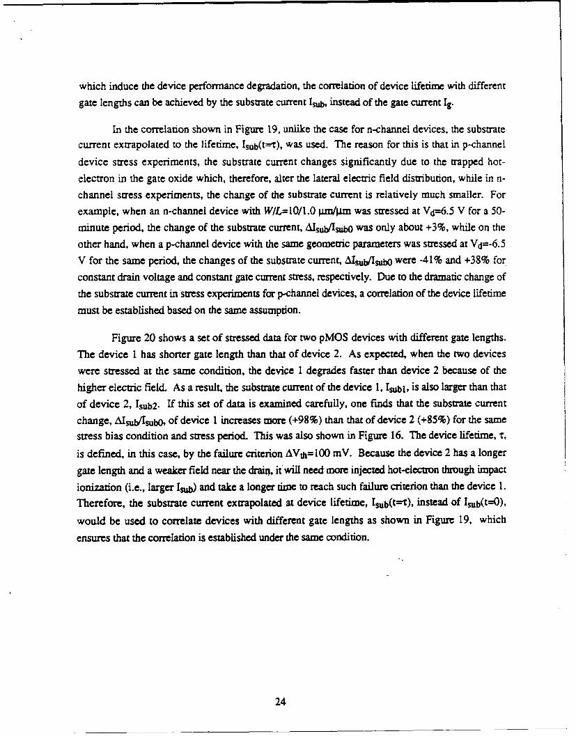
Figure 20 shows a set of stressed data for two pMOS devices with different gate lengths.
The device 1 has shorter gate length than that of device 2. As expected, when the two devices
were stressed at the same condition, the device 1 degrades faster than device 2 because of the
higher electric field. As a result, the substrate current of the device 1, Isub, is also larger than that
of device 2, Isub2. If this set of data is examined carefully, one finds that the substrate current
change, Alsub/IsubO, of device 1 increases more (+98%) than that of device 2 (+85%) for the samestress bias condition and stress period. This was also shown in Figure 16. The device lifetime, r,
is defined, in this case, by the failure criterion AV1=100 mV. Because the device 2 has a longer
gate length and a weaker field near the drain, it will need more injected hot-electron through impact
ionization (i.e., larger Isub) and take a longer wne to reach such failure criterion than the device I.
Therefore, the substrate current extrapolated at device lifetime, Isub(t= ), instead of Isub(t=O),
would be used to correlate devices with different gate lengths as shown in Figure 19, which
ensures that the correlation is established under the same condition.
24
> [ Device 1: 0.5 pun Stress Condition: 10&Device 2:0.9j n Vg-1.5 V
Vdstart-7.0 V
Failurfe Criterion .10 i 2 AVth-lm -00 MV 102
C42 AV2
> 10110~
0 '
lo . 0 1 T 102a2 l10
Stress Time (rai.)
Figure 20. The definition of substrate current used in device lifetime correlation.
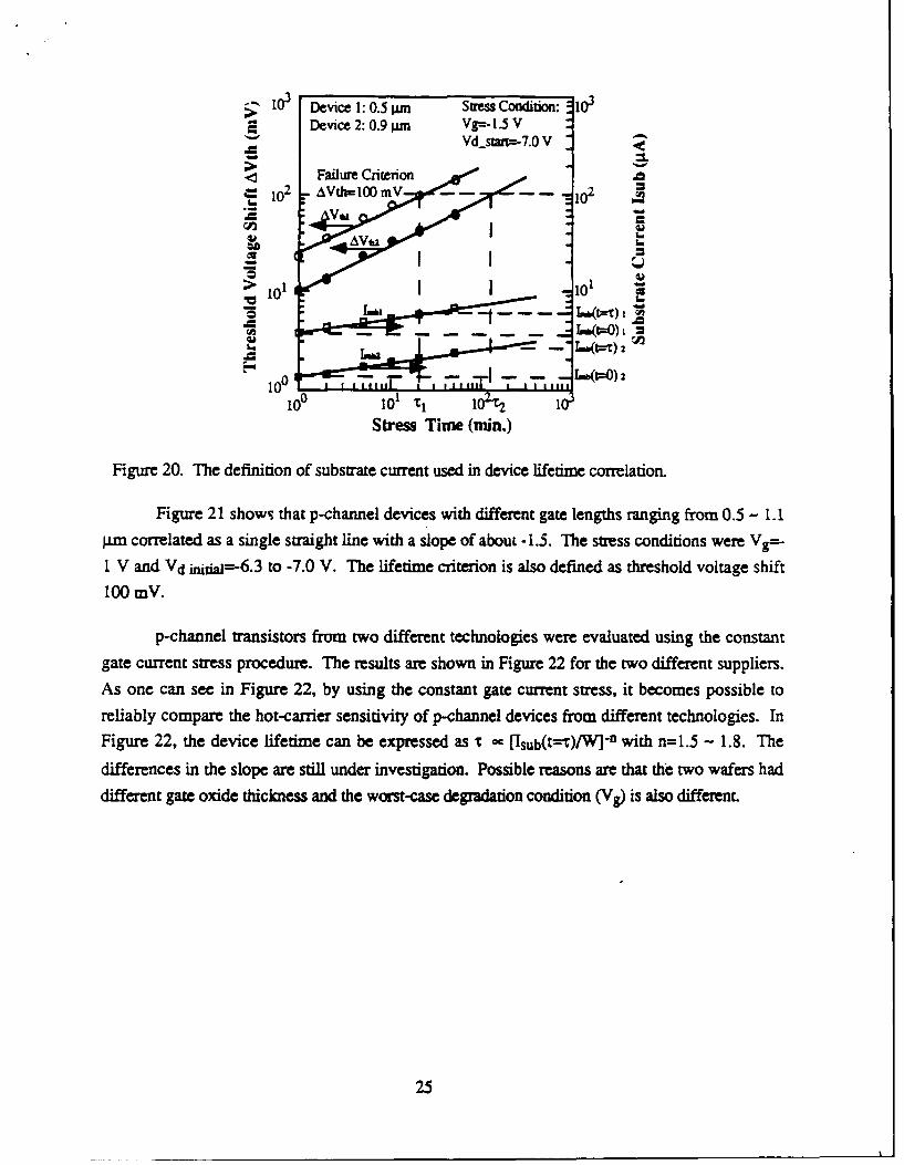
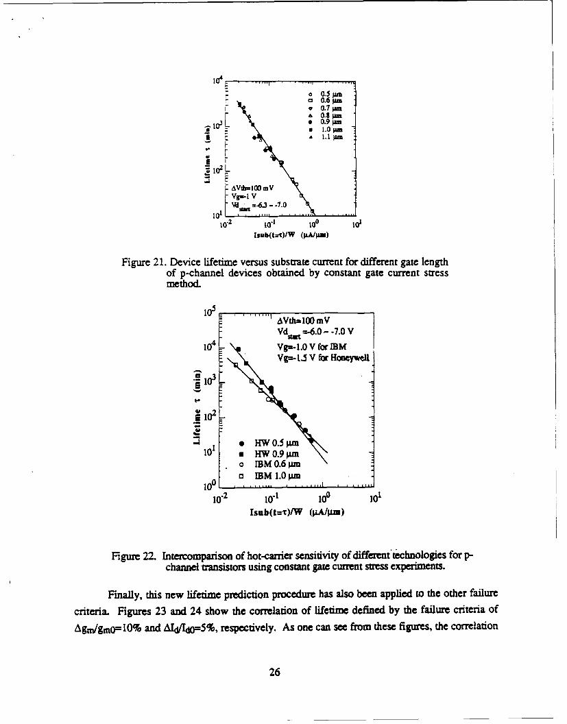
Figure 21 shows that p-channel devices with different gate lengths ranging from 0.5 - 1.1
im correlated as a single straight line with a slope of about -1.5. The stress conditions were Vg=-
1 V and Vd inial=-6 .3 to -7.0 V. The lifetime criterion is also defined as threshold voltage shift
100 mV.
p-channel transistors from two different technologies were evaluated using the constantgate current stress procedure. The results are shown in Figure 22 for the two different suppliers.
As one can see in Figure 22, by using the constant gate current stress, it becomes possible to
reliably compare the hot-carrier sensitivity of p-channel devices from different technologies. InFigure 22, the device lifetime can be expressed as T - [Isub(t---)/W] -n with n=1.5 - 1.8. The
differences in the slope are still under investigation. Possible reasons are that the two wafers had
different gate oxide thickness and the worst-case degradation condition (Vg) is also different.
25
0.5r a O.6 m
r 0 0.7M=
0.9 i1.0 pm
lo,
Vdb= =I 7OD \
10-2 10'1 100 101Isub(t--')/W (gA/jMu)
Figure 21. Device lifetime versus substrate current for different gate lengthof p-channel devices obtained by constant gate current stressmethod.
10 . .. AVth=100 mV
Vdm t t =-6.0 - -7.0 V
104 Vg=-1.o V for IMVg- 1. V for Honeywell
1o3L
*HW 0.5 Pm101 a HW 0.9 PAm
o IBM 0.6 pina BM l.Ogm
10-2 10-1 100 101Isub(t=O/W (iA/In)
Figure 22. Intercomparison of hot-carrier sensitivity of different technologies for p-channel transistors using constant gate current stress experiments.
Finally, this new lifetime prediction procedure has also been applied to the other failure
criteria. Figures 23 and 24 show the correlation of lifetime defined by the failure criteria of
A'gm/gmo=lO% and AId/Ido=5%, respectively. As one can see from these figures, the correlation
26
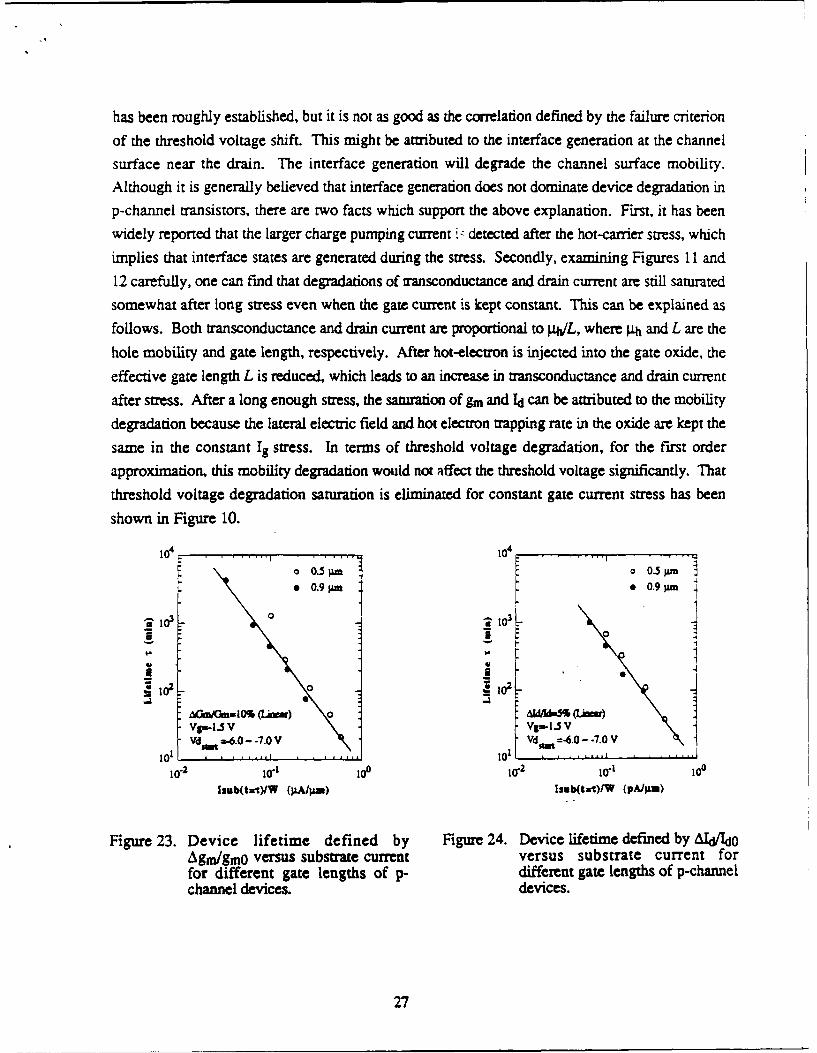
has been roughly established, but it is not as good as the correlation defined by the failure criterion
of the threshold voltage shift. This might be attributed to the interface generation at the channel
surface near the drain. The interface generation will degrade the channel surface mobility.
Although it is generally believed that interface generation does not dominate device degradation in
p-channel transistors, there are two facts which support the above explanation. First, it has been
widely reported that the larger charge pumping current I detected after the hot-carrier stress, which
implies that interface states are generated during the stress. Secondly, examining Figures 11 and
12 carefully, one can find that degradations of transconductance and drain current are still saturated
somewhat after long stress even when the gate current is kept constant. This can be explained as
follows. Both transconductance and drain current are proportional to p4/L, where "±h and L are the
hole mobility and gate length, respectively. After hot-electron is injected into the gate oxide, the
effective gate length L is reduced, which leads to an increase in transconductance and drain current
after stress. After a long enough stress, the saturation of gm and Id can be attributed to the mobility
degradation because the lateral electric field and hot electron trapping rate in the oxide are kept the
same in the constant Ig stress. In terms of threshold voltage degradation, for the first order
approximation, this mobility degradation would not affect the threshold voltage sigrificantly. That
threshold voltage degradation saturation is eliminated for constant gate current stress has been
shown in Figure 10.I (y 00 0.5 am o 0.5la* 0.9 Pin • 0.9 gm
F. i0 2 •102
VhW-l.5 V vs=.I.5 vVdp =40- .7.0V Vd' t =-6.0 0 -. V
10 1 10 1 . , , . .I . . .
10-2 t0- l o l0 "2 10- lO°
Isub~t-r)YW (WM) lsvb~t--W)W (pA/4M)
Figure 23. Device lifetime defined by Figure 24. Device lifetime defined by AJId/loAgm/gmo versus substrate current versus substrate current forfor different gate lengths of p- different gate lengths of p-channelchannel devices, devices.
27
6.0 SOFTWARE FOR THE SIMULATOR
The software developed for the simulator includes modules to control the hardware, test the
device and analyze the data. The major hardware components of the simulator are the
semiconductor parametric tester (HP 4145), the ARACOR Model 4100 Automatic Semiconductor
Irradiation System, and the HP-9816 personal computer. The software is written in HP-BASIC
3.0 which can be converted easily into other high-level computer languages.
The first computer program, called USTRESS, is an extended and modified version of the
Berkeley program used in the Phase I of this program. This program controls the HP4145 tester
and performs the constant drain voltage stress test. The new version of this computer program can
be used to conduct constant drain voltage stress tests for both n- and p-type transistors.
The input parameters of USTRESS are all the necessary parameters to perform the stress
test and data analysis, which includes: (1). the device parameters (i.e., gate length and width,
oxide thickness, substrate doping concentration); (2). stress bias conditions for different terminals
(i.e., gate, source, drain and substrate); (3). stress time parameters (i.e., total stress time, and the
stress time interval pattern to monitor device characteristics); (4). measurement conditions (i.e., the
parameters to be monitored before, between, and after the stress test ).
The device degradation parameters of threshold voltage, Vth, maximum transconductance,
gin, subthreshold slope, Sw, and the drain current, Id, are monitored and recorded in four different
modes (i.e., forward-linear, reverse-linear, forward-saturate and reverse-saturate) during the stress
experiment. The output parameters of USTRESS includes all the time dependence of the device
degradation parameters mentioned above as well as the substrate current, Isub, and gate current, 1g,
changes as a function of stress time. All these output parameters are stored on a floppy disk which
can be read out by the other program module to evaluate the device lifetime.
The second computer program, called IGSTRESS, controls the HP4145 tester and
performs the constant gate current stress test for p-channel transistors. This program can monitor
the gate current at short periods (which can be specified as an input parameter, e.g., 15 seconds)
and adjusts the drain stress voltage automatically to keep the gate current constant. The input
parameters of this program are the same as the USTRESS program, plus the time interval for
monitoring on gate current. The device degradation parameters to be monitored are the same as the
USTRESS program. The output parameters of IGSTRESS ame also the same as the USTRESS,
plus the recorded gate current, substrate current, and the adjusted drain stress voltage during each
gate current monitoring interval. Like the USTRESS program, all the output parameters of
IGSTRESS are stored in a floppy disk for further lifetime evaluation.
28
The third computer program, called LIFETIME, is extended and modified from Phase I toevaluate the device lifetime after hot-carrier stress for both n- and p-channel transistors. Thisprogram takes the output parameters of USTRESS or IGSTRESS as its input parameters. Threedifferent failure criteria (i.e., threshold voltage AVth, transconductance Aggn/gmo and drain currentAd/Id0) can be selected to define the device lifetime. A specification of the failure criterion to beused, such as AVth = 10 mV, is an input. The degradation of device parameters as a function ofstress time can be plotted. The device lifetime extrapolation is performed by this computer
program.
Finally, the last computer program, called RAD, conducts the X-ray irradiation test. Thisprogram controls the ARACOR Model 4100 X-irradiation system and the HP parametric tester. Italso analyzes the device degradation for both n- and p-type transistors after irradiation.
The input parameters of RAD include: (1) the device parameters as described above, (2) thebias conditions during total-dose test for different terminals, (3) the radiation dose parameters (i.e.,the dose rate, total dose and the dose interval pattern to monitor device characteristics), and (4)
measurement conditions.
This program measures the drain current versus gate voltage characteristics in both linearand saturation regions pre- and post- irradiation. It will determine the total threshold voltage shift,AVth, and the threshold voltage due to the build up of oxide charge, AVot, and interface statesgeneration, AVit, respectively. The other degradation parameters to be monitored includesmaximum transconductance change Agm/gm, subthreshold slope Sw and drain current Id. Interface
states generation, ANit or ADit, are calculated by using the subthreshold slope technique. All theseparameters are stored in a floppy disk and can be re-evaluated if necessary.
This program controls the Model 4100 during the irradiation and monitors the devicedegradation using the HP 4145 automatically. By using this program, up to three devices (limitedby the number of SUM of the HP4145) on the same wafer die can be irradiated and analyzedsimultaneously. The total time of the measurement depends mainly on the dose rate to be used.For example, if the dose rate is 1 Mrad(SiO2)/min. it will take about 25 minutes to irradiate threedevices to a total-dose of 20 Mrad(SiO) at which dose level the hot-carrier induced device lifetimecan be extrapolated and correlated reliably. Such measurement time is shorter than theconventional electrical stress test time which usually takes 50 minutes for each individual device.
The four computer program modules for the reliability simulator are stored in a floppy disk.
29
7.0 PHASE II CONCLUSIONS
A real-time reliability simulator to predict device lifetime of n-channel MOSFET transistorsdue to channel hot-electron (CHE) degradation was developed in this Phase II program. The
approach was to generate the interface states by using x-ray irradiation instead of the classical
electrical stress. The benefit of this approach is reduced test time dramatically. The reliability
simulator is now available for use by developers of radiation-hard VLSI microelectronics and
provides a means to perform a reliability screen on Zub-micron CMOS devices and circuits.
The correlation between the x-ray radiation induced and hot-electron induced interface state
generation was established for both conventional non-LDD and the LDD n-channel devices. In
LDD devices, because the source/drain series resistance plays a significant role in both hot-carrier
stress and X-ray radiation tests, the changes in transconductance are not able to provide the
necessary information about the generation of the interface states in these tests. However, it has
been demonstrated in this Phase II program that a simple, fast x-ray radiation te~t does provide auseful means to predict the hot-carrier-induced device lifetime of both conventional and LDD n-
channel MOSFETs by using appropriate failure criteria. In conventional n-MOSFETs, hot-carrier
induced device lifetime, THE, is extrapolated at Isub/W= 5 pA/gin by defining failure criterion
Agm/gm= 3 % or AId/do=3%, while THE for LDD devices, T. is extrapolated at Iub/W= 5 WAtnn
by defining failure criterion AVth=10 mV. Radiation figure-of-merit, Deft, is defined as the total
dose where the interface generation, ANit, is increased to the level of 5 x 10¹¹ cra-2 . This is
equivalent to transconductance degradation AgwJgm=50 % in non-LDD devices. Such correlation
has been confirmed by the charge pumping measurements. Seven types of LDD devices from
different process technologies have been tested and correlated as shown in this report. An n-
channel SIMOX device also appears to fit the same correlation.
A new hot-carrier stress test procedure has been developed to evaluate the hot-carrier
induced device lifetime of p-channel transistors. Unlike the conventional constant voltage stress,
the gate current is monitored and maintained constant during the stress by adjusting the drain stress
voltage at short-time intervals. This approach ensures a constant electric field near the drain and
the constant electron injection rate. It eliminates the degradation saturation effect which usually
occurs in the conventional constant voltage stress test and prevents extrapolation of reliable device
lifetime. In order to compare hot-carrier sensitivity, it is desirable to correlate the devices with
different gate lengths from the same process technology into one straight line. This has been
achieved by utilizing the substrate current extrapolated at lifetime Im1(t-t), rather than the substrate
current at the beginning Isub(O), as the hot-carrier generation indicator. Therefore, by combining
30
the constant gate current stress and the new lifetime extrapolation procedure, it becomes possible to
compare the hot-carrier sensitivity of different process technologies. The correlation between x-ray
irradiation and hot-carrier induced degradation in p-channel transistors has not been established.However, further study is needed to investigate the relationship of the neutral hole trappingproduced in x-ray irradiation and the neutral electron trapping produced by hot-carrier stress.
The hardware of the simulator includes an HP-4145 semiconductor parametric tester andthe ARACOR Model 4100 Automatic Semiconductor Irradiation System. Different software was
developed to control the hardware of the simulator, collect the data and perform the data analysis.The simulator is capable of irradiating three devices to a total-dose of 20 Mrad(SiO 2 )
simultaneously in about 25 minutes, at which dose level the hot-carrier induced device lifetime canbe extrapolated and correlated reliably. Such a measurement time is much shorter than the
conventional electrical stress test time which usually takes 50 minutes for each individual device.
Because this new simulation technique is easy to use, fast, and accurate, it can greatly
reduce the cost and improve the efficiency of implementing the type of high reliability screen
required for the VLSI circuits used in many space and military applications.
8.0 ACKNOWLEDGEMENT
This work was supported by SDIO under DNA contract No. DNA001-89-0194. Wegratefully acknowledge guidance provided by LL Commander L. Cohn, RAEE of DNA. Thehelpful technical direction and suggestions provided by Dr. L. J. Palkuti, RAEE of DNA, are also
greatly appreciated and acknowledged. We would like to thank the following individuals and
organization for supporting this work by providing test samples: J. Schrankler, Honeywell; R.A.
Kohler, AT&T; W. Bailey, TI; N. Haddad, IBM; and L. Walsh, National Semiconductor Corp.
We gratefully acknowledge Q. M. Zhang, University of Toronto, for 2-D device simulation.
9.0 REFERENCES
[1]. K.K. Ng and G.W. Taylor, "Effects of Hot-carrier Trapping in n- and p-MOSFE1s", IEEETrans. on Electron Devices, Vol. ED-30, pp. 871-876 (1983)
f2j. C.M. Hu, S. Tam, F-C Hsu, P.K. Ko, T-Y. Chan, and K.W. Texllt Hot-Electron-InducedMOSFET Degradation- Model, Monitor, and Improvement", IEEE Trans. on ElectronDevices, Vol. ED-32, pp. 375-385 (1985)
[3]. P.J. Mcwhorter and P.S. Winokur, "Simple Technique for Separating the Effects of theInterface Traps and Trapped Oxide Charge in Metal-oxide-Semiconductor Transistors",Appi. Phys. Let., Vol. 48(2), pp.133-135 (1986)
31
)
[4]. L. Palkuti, R.D. Ormond, C.M. Hu and J. Chung, "Correlation between channel Hot-Electron degradation and Radiation induced-interface interface trappings in MOS devices".IEEE Trans. on Nuclear Science, Vol. NS - 37(6) 1989
[5]. J.Y. Choi, P.K. Ko and C.M. Hu, "AC versus DC stressing", Dig. Tech. Pap. !EEE/JSAPSymp. VLSI Technol. 1987, pp. 45-46 (1987)
[6]. P. Heremans, H.E. Maes and N. Saks "Evaluation of Hot-Carrier Degradation of N-channelMOSFETs with the Charge Pumping Technique", IEEE Electron Devices Let., EDL-7(7),pp. 428-430 (1986)
[7]. K.F. Galloway, M. Gaitan and T.J. Russell, "A simple model for separating interface andoxide charge effects in MOS device characteristics". IEEE Trans. on Nuclear Science, Vol.NS - 31(6), pp.1497-1501, 1984.
[8]. F.W. Sexton and J R. Schwank, "Correlation of radiation effects in transistors and integratedcircuits". IEEE Trans. on Nuclear Science, Vol. NS - 32(6) pp.3975-3981, 1985.
[9]. F.-C. Hsu and H.R. Grinolds, "Structure-dependent MOSFET degradation dute to hotelectron injection". IEDM., Tech. Dig., 1983
[10]. F.-C. Hsu and K.Y. Chiu, "Evaluation of LDD MOSFETs based on hot-electron induceddegradation". IEEE Electrical Devices Let., Vol. EDL- 5 1984
[11]. X.M. Li and M.J. Deen, "A new charge pumping method for determination of spatialinterface state density distribution in MOSFETs", IEDM., Tech. Dig., 1990
[12]. M.G. Ancona, N.S. Saks and D. McCarthy, "Lateral distribution of hot-carrier-inducedinterface traps in MOSFETs", IEEE Trans. on Electron Devices, Vol. ED-35(12), pp.2221-2228 (1988)
[131. T. Poorter and P. Zoestbergen, "Hot carrier effects in MOS transistors". IEDM., Tech.Dig., pp. 100-103, 1983
[14]. Q.M. Zhang, G.L. Tan, J.M. Xu and D.J. Day, "Current gain and transit-time effects inHBTs with graded emitter and base regions" IEEE Electrical Devices Let., Vol. EDL -11, No. 11, pp. 508-510, 1984
[15]. T. Kaga and Y. Sakai, IEEE Trans. on Electron Devices, Vol. ED-35(12), p. 2384, 1988
[16]. J. J. Tzou and et al, IEEE Electron Device Letters, Vol. 7(1), p.5 1986
[17]. Y. Hiruta and et al., ESSDERC Tech. Digest, p.733, 1989
[18]. M. P. Brassington and R. R. Razouk, "Relationship between gate bias and hot-carrierinduced instabilities 1987 Symp. on VLSI Tech.., Tech. Digest,.p.55
[19]. P. Heremans, R. Bellens, G. Groseneken and H. Maes, "Consistent model for the hot-carrier degradation in n-channel and p-channel MOSFETs",. IEEE Trans. on ElectronDevices, Vol. ED-35(12), p. 2194, 1988
[20]. Q. Wang, M. Brox, W.H. Krautschneider and W. Weber, "Explanation and model for thelogarithmic time dependence of p-MOSFET degradation, IEEE Electron Device Letters, VoL12(5), p.2 18 1991
32
[21]. W. Weber and F. Lau, "Hot-carrier drifts in subinicrometer p-channel MOSFETs". IEEEElectrical Devices Lett., Vol. EDL - 8(5). p.208. 1987
(22]. M. P. Brassington, M.W. Poulter and M. E1-Diwany, "Supperssion of hot-carrier effects insubmicrometer surface-channel PMOSFETs",. IEEE Trans. on Electron Devices, Vol. ED-35(7), p. 1149, 1988
(23]. T.C. Ong, P.K. Ko and C.M. Hu, "Hot-carrier current modeling and device degradation insurface-channel p-MOSFET's",. IEEE Trans. on Electron Devices, Vol. ED-37(7), p.1658, 1990
(241. C.M. Hu, S. Tam, F-C Hsu, P.K. Ko, T-Y. Chan, and K.W. Terrill, "Hot-Electron-Induced MOSFET Degradation-- Model, Monitor, and Improvement", IEEE Trans. onElectron Devices, ED-32, pp. 375-385 (1985)
[25]. C. Hu, "Hot -carrier effects", chpt. 3, in "Advanced MOS Device Physics" (N.G.Einspruch, ed.) p. 129. Academic Press Inc. (1989)
33