ad-a243 524 annual letter report - dticrobert f. davis, zlatko sitar, michael j. paisley, joe j....
TRANSCRIPT

AD-A243 524
Annual Letter Report
Growth, Nitrogen Vacancy Reduction and Solid SolutionFormation in Cubic GaN Thin Films and the Subsequent
Fabrication of Superlattice Structures Using AIN and InN
Supported under Grant #N00014-86-K-0686 P5Innovative Science and Technology Office
of the Strategic Defense InitiativeOffice of the Chief of Naval Research
Report for the period January 1, 1991-December 31, 1991
Robert F. Davis, Zlatko Sitar, Michael J. Paisley, Joe J. Sumakeris,Laura Smith, K. Shaun Ailey-Trent, and Dong W. Kum
Materials Science and Engineering DepartmentNorth Carolina State University
Campus Box 7907Raleigh, NC 27695-7907
t - i,, tion Unfmited
December, 1991
I 91-18137I tiII I1 II n lI ililt II Ii

I lOfm .1jptoved
REPORT DOCUMENTATION PAGE O4m No 0 J 0f,18
0.r..f *.in , f . ft#j 0. 'W 99, 'n I*, O . '9.)r*41eP C*" PtIi " *. -* f * '.1 c .re 'a, " r IA f Ct *. *ae. A %#.nJF% .. *,.9,- *.*q 3696 tAS9%
1. AGENCY USE ONLY , Oijnk) j 2. REPORT DATE I 3. REPORT TYPE AND OATES COVERED
7 December, 1991 Annual Letter 1/1/91-12/31/91II4. TITLE AND SUBTITLE Growth, Nitrogen Vacancy Reduction and S. FUNDING NUMBERSSolid Solution Formation in Cubic GaN Thin Films and the R&T:s400001srq05Subsequent Fabrication of Superlattice Structures Using S.O.:iII4SSAlN and InN
6. AUTHOR(S)
3 Robert F. Davis
7. PERFORMING ORUANIZATION NAME(S) AND AODRESS(ES) 6. PEqFORMING ORGANIZATIONREPORT NUMBER
North Carolina State UniversityHillaborough Street N00014-86-K-0686 P5Ralegh,NC 21695
9. SPONSORING/ MONITORING AGENCY NAME(S) AND ADORESS(ES) 10. SPONSORING; MONITORINGSponsoring: ONR, 800 N. Quincy, Arlington, VA 22217 AGENCY REPORT NUMBER
Monitoring: Office of Naval Research Resider, N66005I The Ohio State University Research Center1314 Kinnear RoadColumbus, OH 43212-1194
I I. SUPPLEMENTARY NOTES
I 12a. DISTRIBUTION I AVAILA6ILITY STATEMENT 12b. OISTRIBUTION CODE
3 Approved for Public Release; Distribution Unlimited
I. ABSTRACT (d4Aimwm9j0v00 oudS)An atomic layer epitaxy deposition system configured for the growth of thin films of the rI-V nitridesof Al, Ga and In has been designed, constructed and commissioned. The system allows the introductionof up to 16 gases without mixing. Self-terminating growth of crystalline GaN films has been achievedon single crystal wafers of (0001) a(6H)-SiC. Results of analyses via Auger spectroscopy, electronmicroscopy and electron diffraction are described. Deposition of AIN and GaN via gas-source MBEwas also continued during this period. The principal emphasis concerned the initial stages of growth ofboth compounds on the substrates of (00001) a(6H)-SiC and (0001) sapphire, as determined using X-ray photoelectron spectroscopy. An initial layer of silicon nitride formed on the surface of SiC prior tothe deposition of either nitride. The deposition of GaN on sapphire followed the Stranski-Krastanovmode of nucleation and growth, while on SiC, characteristics of three-dimensional growth were evident.By contrast, AIN grew initially in a layer-by-layer mode. Deposition of GaN on vicinal (100) P-SiCduring UV irradiation resulted in the formation of a new 4H polytype of this material. Deposition of BNvia gas-source MBE on Cu(1 10) resulted in nanocrystalline cBN; films grown on (I 11) Cu resulted inh-BN (graphitic phase). Similar studies using Si(100) substrates also resulted in the occurrence of cBN.The occurrence of the cubic polytype was enhanced while that of h-BN was discouraged with the use ofthe UV light at 400-5000 C.
14. SUBJECT TERMS I IS NuMBEI Of PAG Sgallium nitride, aluminum nitride, boron nitride, atomic layer epitaxy, 76layered structures, transmission electron microscopy, photoluminescence, 16 PRICE coDEgas-source MBE, laser ablation, borazine
17. SECURITY CLASSIFICATION 1I. SICURITY CLASSIFICATION 19. SECURITY CLASSIFICATION 20 LIMITATION Of ABSTRACTOF REPORT OF THIS PAGE OF ABSTRACT
UNCLAS UNCLAS UNCLAS SAR
J., 15 Au 0 1. -d A 'S 1 .4

Table of Contents
I. Introduction 1
II. Atomic Layer Epitaxy of Gallium Nitride 1
A. Introduction 1B. Experimental Procedure 2
1. Description of the HI-V Nitride ALE System 22. Growth Theory 53. Growth and Analysis Procedures 6
C. Experimental Results and Discussion 71. Surface Morphology 72. Chemical Analysis 83. Electron Diffraction 8
D. Conclusions 9E. Future Research 9F. References 9
III. Interface Chemistry and Surface Morphology in the Initial 10Stages of Growth of GaN and AIN on a-SiC and Sapphire
A. Introduction 10B. Experimental Procedures 12
1. Deposition System 122. Film Growth 133. XPS Analysis 14
C. Results and Discussion 171. Growth Morphology: GaN 172. Growth Morphology: AIN 203. Interface Chemistry: GaN 214. Interface Chemistry: AIN 23
D. Conclusions 27E. Future Research Plans 28F. References 28
IV. Gas-Source Molecular Beam Epitaxy of Boron Nitride 29and Gallium Nitride
A. Introduction 29 A,. ..1. Boron Nitride 29-2. Gallium Nitride 301 r ,3. Photo-Enhanced Growth 30 !~4- ?aa
Thermal Effects 31 uatI2 1 ,,, U d
Enhanced Atom Mobility 31 Juata t lea t
Photolytic Decomposition / © 32 .Dopant Activation C 32 f . . . .Other Photochemical Effects PI 32 Dis t , t t,./Conclusions on Photo-Enhancement 35 Av,1Ab l . lie
B. Experimental Procedure 35 Aar, ,' .C. Results 38 DIA1 ipe l
1. Boron Nitride 38Boron Nitride on Copper 38iU

C. Results ContinuedBoron Nitride on Silicon (100) 39
2. Gallium Nitride 46D. Discussion 56
1. Boron Nitride 56Boron Nitride on Copper 56Boron Nitride on Silicon (100) 57
2. Gaflium Nitride 58E. Conclusions 60
1. Boron Nitride 60Boron Nitride on Copper 60Boron Nitride on Silicon (100) 60
2. Gallium Nitride 61F. Future Research Plans/Goals 61
1. Boron Nitride 61Boron Nitride on Copper 61Boron Nitride on Silicon (100) 61
2. Gallium Nitride 61G. References 62
Appendix 1 64

II. INTRODUCTION
Continued development and commercialization of optoelectronic devices, including light-
emitting diodes and semiconductor lasers produced from II-V gallium arsenide-basedmaterials, has also generated interest in the much wider bandgap semiconductor mononitride3materials containing boron, aluminum, gallium, and indium. The majority of the studies havebeen conducted on pure gallium nitride thin films having the wurtzite structure, and thisemphasis continues to the present day. Recent research has resulted in the fabrication of p-njunctions in both wurtzite gallium nitride and cubic boron nitride, the deposition of cubicgallium nitride, as well as the fabrication of multilayer heterostructures and the formation of
thin film solid solutions. Chemical vapor deposition (CVD) has usually been the technique of
choice for thin film fabrication. However, more recently these materials have also been
deposited by plasma-assisted CVD, reactive ionized-cluster beam deposition and reactive andionized molecular beam epitaxy.
The program objectives in this reporting period have been (1) the continued development
and employment of atomic layer epitaxy as a low temperature deposition method for GaN (2)the determination of the chemistry and morphology inherent in the nucleation and growth ofGaN and AIN on the substrates of ct(6H)-SiC (0001) and sapphire (A12 0 3) (0001) via gas-
source molecular beam epitaxy (GSMBE) and (3) the deposition of films of GaN and BN
using GSMBE and microwave plasma chemical vapor deposition. The procedures, results,
discussions of these results and conclusions of these studies are given in the following
sections. Note that each major section is self-contained with its own figures, tables andreferences.
II. ATOMIC LAYER EPITAXY OF GALLIUM NITRIDEA. Introduction
At the present time, MBE and MOCVD are the two contenders for the growth of the mostsophisticated semiconducting structures. Both can produce extremely thin layers and a widerange of compound semiconductors and heterostructures. However, in both techniques all thereactant species arrive simultaneously to the substrate. As such, the growth of the subsequent3 monolayer of the material may be initiated before the growth of the previous one is
completed. As a result, the growth process occurs on several levels of monolayers. This
occurs in practically all materials deposition systems and is easily observed via RHEED
oscillations. One observes the damping of the oscillation amplitude with the film thickness.
As a result, the RHEED oscillations usually disappear after 10-20 monolayers of growth.
The ultimate technique, with the best control over the composition and the surfacemorphology, may be the deposition of a single layer of the atoms of one of the components at3 a time. The single most successful method for achieving this is by Atomic Layer Epitaxy

I
(ALE), a technique patented by Suntola and Atson in 1977 [1]. They used this method for the
deposition of the polycrystalline ZnSe on glass substrates because of their concern regarding
thickness uniformity over large areas.
Initially it was thought that ALE was applicable only for II-VI compounds. However, it
i has been shown that it also works also for other compounds and elements. A comprehensive
review of the ALE research on II-VI compounds has been published by Goodman and Pessa
[2]. Considerable attention has been lately devoted to the ALE of GaAs, and several research
groups have demonstrated the feasibility of the technique for Ga-based III-V compounds
[3,4].
Atomic Layer Epitaxy can be achieved with many existing deposition techniques, and is
best thought of as a special mode of operation of the known techniques, rather than an
entirely new deposition method. Since ALE consists of deposition cycles in which a single
monolayer of individual species is deposited at a time, the final film thickness depends only
on the number of cycles and the lattice parameter of the material. Thus ALE offers the
ultimate control over the thickness and morphology of the layers, and has also the potential
for the achievement of very good stoichiometry and the reduction of point defects. Since the
reactants remain separated throughout the deposition, homogeneous nucleation of the desired
phase within the gas stream is minimized.
B. Experimental Procedure
1. Description of the II-V Nitride ALE System
To accomplish ALE of the III-V nitrides, a vacuum system has been designed, fabricated
and commissioned which allows ALE deposition within the framework of organometallic
(OM) CVD parameters. The system is configured to process one-inch wafers. Ultimately, the
apparatus may be adapted to handle samples up to two inches in diameter. The system
consists of three chambers; a load lock, a cleaning chamber and a growth chamber. It is made
of stainless steel parts with knife edge seals and is high vacuum capable. Process gasses are
regulated by mass flow controllers and pumped by a rotary vane pump. The ultimate vacuum
is achieved by diffusion pumps.
The load lock is a simple five way cross that can hold up to five samples. All samples are
introduced to and removed from the system through this chamber, it can be evacuated to the
millitorr level.
After passing through the load lock, the samples are cleaned in a subsequent chamber
using a remote argon plasma with the downstream injection of hydrogen. The cleaning
chamber is evacuated to high vacuum using a diffusion pump, while the process gases used
for cleaning are handled by a rotary vane pump through an automatic throttle valve. To
assure identical sample cleaning within a run, up to four samples can be cleaned at a time.
2

I
This chamber is capable of performing many variations on the plasma cleaning operation,
since it has the capability of varying gas flow rates, substrate temperature, plasma intensity
and process pressure.
After cleaning, the samples are transferred to the growth chamber. This chamber is also
3 evacuated to high vacuum using a diffusion pump with an LN 2 trap, while the process gases
are handled by a rotary vane pump. The volatile exhaust gases in the growth and cleaning
chambers are diluted with nitrogen and cleaned in a water scrubber prior to the release into
central exhaust system. The process pressure is monitored and controlled by a capacitance
3 pressure gauge and an automatic throttle valve. Inside the growth chamber, the samples sit on
a revolving, heated, disk-shaped holder made of SiC-coated graphite. The overall design
allows sample heating to 1000'C. However, the intention is to process at substantially lower
temperatures. Due to the large mass and the possible use of the high temperature capability,
appropriate heat shielding and water cooling have been installed, as can be seen in the cross-
3 sectional view of the system, shown in Figure 1.
3 Cracking FilamentVane Assembly
I Traveler I Sample Receiver I'
In Iat Shield Element
Power Leads
[ 3 SiC Coated Graphite 316 Stainless Steel
] Alumina Q Water Cooled Cavity
Figure 1. Cross-sectional view of the ALE growth chamber for the deposition of III-Vnitrides.
A specially designed vane assembly allows the deposition in the ALE mode. The
assembly is stationary above the rotating susceptor and consists of sixteen separate
compartments for the introduction of up to eight different process gases without mixing. As
wafers travel under each compartment, they experience a different atmosphere. However, the
3 ALE process requires a purge cycle with an inert gas between each exposure of the wafers to
the reactants. This prevents mixing of the reactant gases and allows time for the desorption of
I physisorbed molecules. After this cycle only the chemisorbed monolayer remains. If a purge
is applied after every exposure to reactants, half of the zones (eight) remain for the
3 deposition. That means four zones for each reactant when a binary compound is grown. This
13
I
arrangement allows the growth of four monolayers of each element (about 7-10 A) of the
binary compound per revolution of the susceptor. The anticipated growth rate in the ALE
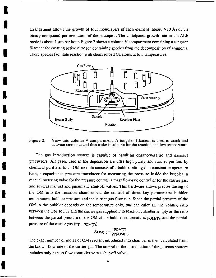
mode is about 1 .m per hour. Figure 2 shows a column V compartment containing a tungstenfilament for creating active nitrogen containing species from the decomposition of ammonia.3These species facilitate reaction with chemisorbed Ga atoms at low temperatures.
IG
Heater Body Sampl Receiver Plate S
_ __ Rotation
Figure 2. View into column V compartment. A tungsten filament is used to crack andactivate ammonia and thus make it suitable for the reaction at a low temperature.
The gas introduction system is capable of handling organometallic and gaseous
precursors. All gases used in the deposition are ultra high purity and further purified by
chemical purifiers. Each OM module consists of a bubbler sitting in a constant temperaturebath, a capacitance pressure transducer for measuring the pressure inside the bubbler, amanual metering valve for the pressure control, a mass flow-rate controller for the carrier gas,
and several manual and pneumatic shut-off valves. This hardware allows precise dosing ofthe OM into the reaction chamber via the control of three key parameters: bubbler
temperature, bubbler pressure and the carrier gas flow rate. Since the partial pressure of theOM in the bubbler depends on the temperature only, one can calculate the volume ratio
between the OM source and the carrier gas supplied into reaction chamber simply as the ratiobetween the partial pressure of the OM at the bubbler temperature, POM(T), and the partialpressure of the carrier gas (PT - POM(T)).
=OM POM('I
XOM(Tm Pt-POM(T)
The exact number of moles of OM reactant introduced into chamber is then calculated fromthe known flow rate of the carrier gas. The control of the introduction of the gaseous sources
includes only a mass flow controller with a shut-off valve.
£ 4

I
1 2. Growth Theory
Several different inorganic and organic precursors have been considered for the ALE of3GaN. Organometallics were chosen over chlorides for the source of Ga because of high
purity, ease of transport from the source to the chamber, and excellent control over dosing.
Triethylgallium was chosen over trimethylgallium for two reasons: (1) lower decomposition
temperature and thus lower growth temperature, which would reduce the concentration of
nitrogen vacancies, and (2) cleaner surface reaction (the decomposition of trimethyl species
often results in the decomposition of the higher deposition methyl radical resulting in residual
C atoms which become incorporated in the growing film). Ammonia was chosen over
hydrazine and nitrogen fluoride mainly because of safety considerations and cleanliness.Ammonia is available in research grade purity. Moreover, chemical ammonia purifiers,which effectively remove remaining water, oxygen and carbohydrides, are also available.
The reaction energy budget these precursors offer theoretically favors the self-limiting
ALE deposition of III-V nitrides on (0001) surfaces of wurtzite or (111) surfaces of
zincblende substrates. The growth direction is crucial, because the number of bonds a
particular species makes on the surface varies greatly with the growth direction. A constituent
of a tetrahedrally bonded compound can make one surface bond in the (0001-) direction, two
surface bonds in (1011) direction and three surface bonds in (0001) direction.
An estimate of whether a reaction is favored or not, can be made by comparing the bondenergies of the reactants and products. The bond energies between Group III metals and
nitrogen, calculated using different methods, are summarized in Table I. For example,
suppose, the (0001) surface is terminated with Ga(C2H5)2 which makes one bond with the
underlaying nitrogen. The subsequent exposure of these adsorbed species to ammonia causes
a surface reaction to occur, if making three bonds with Ga is energetically favorable for the
ammonia molecule. The process will end with a hydrogen terminated surface which does not
react further with ammonia. The bond energy between Ga and the ethyl radical is 57kcal/mol, and the average bond energy between nitrogen and hydrogen is about 90 kcal/mol.
Table I. Bond energies between Ill metals and nitrogen obtained by different methods.
B - N Al - N Ga-N In - N Remarks115 125 108 105 Pauling's formula [6]94 90 65 54 Geometrical mean with correction [6]
83-193 52-122 55-85 47-67 Immediate neighbors72-91 64-80 55-69 49-61 Periodic behavior
66 67(81) 50(56) 49 Heat of vaporization [7]87 94 69 58 Heat of formation [81
85±5 75±5 65±5 55±5 Suggested values
1 5

I
Thus, the total enthalpy to break the necessary bonds within the precursors is
(3x57) + (2x90) = 351 kcal/mol. On the other hand, the enthalpy of formation of each N-Ga
bond releases 65 kcal/mol, and the reaction C2H5 + H -- C2H6 produces about 100 kcal/mol.
Thus, the total enthalpy of reaction is: 3x65 + 2x100 = 395 kcal/mol. Since the energy of
3 reaction is larger than the decomposition energy, the overall reaction to form a H-terminated
N-Ga bilayer is favorable.
A similar calculation can be done for the next Ga layer. The Ga cycle starts with a
hydrogen terminated nitrogen surface. Arriving TEG chemically adsorbs onto the surface by
breaking one H-N bond (90 kcal/mol) and one Ga-ethyl bond (57 kcal/mol) and making one
Ga-N bond (65 kcal/mol) and one C-H bond (100 kcal/mol) producing C2H6 . The energy
balance is 147:165 and the reaction is favorable for the deposition of a Ga layer.
The same calculation is valid also for AIN and BN. The only III metal with a marginal
outcome is In, as can be seen from the data in Table I. However, such calculations offer only3 a rough estimate, since (1) data on bond energies are often inaccurate and (2) the enthalpy of
transformation from the gas to solid state has been neglected. Energy requirements on a3 surface which acts as a catalyst may be even lower.Figure 3 details the ALE process for gallium nitride from triethylgallium and ammonia as
it occurs in our system. A clean, oxide-free 6H- SiC surface (A) is exposed to TEG which
undergoes chemisorption involving rupture of some of the Ga-C2H 5 bonds (B) until a
continuous layer of adsorbed species is formed (C). Subsequently, the samples are exposed to
an ammonia flux flowing across a hot filament (D). The ammonia attaches to the galliumprecursor, replacing any previous termination until a complete layer of the NH 2 radical forms3 as shown in (E) At this point the sample may be again exposed to the TEG and the complete
process repeated (F).
1 3. Growth and Analysis Procedures
In order to test and characterize the new equipment and the overall process, several3 deposition runs were made using different growth parameters. Table II gives the ranges overwhich the various parameters were varied. Throughout the test depositions four of the sixteen
zones were used for TMG, four for ammonia and eight for the hydrogen purge gas.
Reflection High Energy Electron Diffraction (RHEED) was used to determine the
crystallinity and structure of the grown films. Scanning Auger microscopy (JEOL JAMP-30)
was performed to determine the presence of impurities and the nominal composition of the
GaN layers. The surface morphology of the films was characterized using scanning electron
microscopy (Hitachi S-530). Film thickness was measured by using a Rudolph automatic
ellipsometer.
6

A B
D E F
Figure 3. Schematic presentation of GaN ALE process using TEG and ammonia.
Table II. Growth parameters.
Growth temperature 350 - 6500CGrowth pressure 0.5 - 50 TorrAmmonia flow rate 100 - 300 sccmH2 (purge) flow rate 200 - 300 sccmH2(OM carrier) flow rate 50 - 100 sccmTEGa bubbler temperature -10 - 200CTEGa bubbler pressure 400 - 800 TorrRotation speed 1 - 2 RPM
C. Experimental Results and Discussion1. Surface Morphology
Initially, a few CVD runs were attempted, where all reactants were introduced into the
same growth zone. The substrate temperature range was, 750-850 0 C. This did not result in
the growth of GaN films. Onl' large (>10 4rm) individual GaN crystals were observed on the
surface. These were a possible result of homogeneous nucleation in the gas phase.
After a few unsuccessful experiments, the reactants were separated and distributed to the
different growth zones. Substrates were rotated and sequentially exposed to different
reactants. Films were grown at a constant chamber pressure of 50 Torr. The other parameters
of growth temperature, flow rate, and substrate rotation speed (exposure time to each reactant
gas) were changed.
I 7
I
Three dimensional growth was obtained at temperatures higher than 600'C, where
individual crystallites were clearly seen. All of them had either a hexagonal or a triangular
shape, both of which indicated a hexagonal structure. All of them were oriented in the same
direction. The (00011 planes were perpendicular to the surface and the ( 10101 planes of the
I individual crystallites were parallel to each other. This indicated a good epitaxial relationshipwith the ox(6H)-SiC substrate.
Films grown at temperatures lover than 400'C were continuous with no detectable
surface morphology. Ga-rich films with Ga precipitates were obtained, when the same flow
conditions were used as for the high temperature runs. When the supply of TEG was reduced
by about three times, a clean GaN film without Ga precipitates was obtained. However, this3 reduced the growth rate form 2000 A/hr to 600 A/hr.
2. Chemical Analysis3 Scanning Auger microscopy was performed on the samples to determine both the
presence of impurities and the nominal composition of the GaN layers. No contaminants
were observed within the resolution of the instrument (typically =0.1 at.%). Comparison of
the Auger spectra of these films with those grown via MBE showed the ALE materials to be
stoichiometric.
3. Electron Diffraction3Reflection high-energy electron diffraction (RHEED) was performed on the GaN films.
All films showed a distinct diffraction pattern indicative of the wurtzite structure. The films
grown at high temperatures showed spotty diff-action patterns, in agreement with the rough
surface morphology observed via SEM. The film. grown at low temperature showed streakeddiffraction patterns indicative of a smooth surface, as well as Kikuchi lines indicative of good
crystallinity.The main aim of this research was to determine the experimental window in which GaN
grows in a truly self-terminating process. Figure 4 shows the dependence of the amount offilm grown per cycle with respect to the residence time per reaction zone. One can see that
the growth per cycle initially increases quickly with exposure time but becomes more gradual
after =10 sec. of exposure. Although these growth conditions could be utilized for layer-by-
layer growth by correctly adjusting each exposure time, the process was not self-terminating
at this temperature.
Subsequently, GaN films were grown at a sample temperature of 280'C. The crystallinity
of these films has been confirmed by crystal x-ray diffraction. At an exposure time of 22
seconds, the growth rate corresponded to 2.62 A per cycle, which corresponds to one
monolayer of molecular coverage. When the growth was performed with an exposure time of
8

Coverage/ Cycle vs Zone/ Cycle (360'C)
7GaN Info.
6 a = 3.19Ac = 5.189A
5-IZ4 - cen
L.3- edge
2-0
0* . ,•
0 20 40 60 80 100sec/zone
Figure 4. Dependence of the amount of film grown per cycle with respect to the residencetime per reaction zone at a growth temperature of 360'C.
11 seconds the coverage per cycle falls to 1.2 A per cycle. Recent mechanical difficulties
with the system have prevented us from repeating the run for exposure times greater than 22
seconds, in order to determine if the coverage per cycle will remain unchanged at one
monolayer per cycle.
D. Conclusions
The first results of the ALE growth of GaN are very encouraging. The system has
performed well, and very low temperature growth of GaN has been achieved. The films were
chemically stoichiometric crystalline and with a very smooth surface.
E. Future Research
Efforts to achieve a truly self-terminating layer-by-layer growth of both GaN and AIN
and their solid solutions and heterostructures will be continued. Films of sufficient thickness
(0.5 jtm) will be grown in order to conduct electrical and luminescent measurements.
F. References
1. T. Suntola and J. Atson, U.S. Patent 4 058 430, Nov. 15 (1977).2. C.H.L. Goodman and M.V. Pessa, J. Appl. Phys. 60, R65 (1986).3. S.M. Bedair, M. Tischler, T. Katsuyama, N.A. El-Masry, Appl. Phys. Lett. 47, 51 (1985).4. J. Nishizawa, H. Abe and T. Kurabayashi, J. Electrochem. Soc. 132, 1197 (1985).5. R. C. Weast ed., Handbook of Chemistry and Physics, 69thEdition 1988-1989, CRC
Press, Inc., Boca Raton, Florida.6. L. Pauling, The Chemical Bond, Cornell University Press, N.Y., 1967.7. V. I. Vedeneev, Bond Energies, Ionization Potentials and Electron Affinities, St Martin's
Press, N.Y., 1966.8. T. L. Cottrel, The Strengths of Chemical Bonds, Butterworths Scientific Publications,
London, UK, 1954.
9
III. INTERFACE CHEMISTRY AND SURFACE MORPHOLOGv INTHE INITIAL STAGES OF GROWTH OF GaN AND AIN ON a-SiCAND SAPPHIRE
A. IntroductionSuccessful commercialization of infrared and selected visible light-emitting
optoelectronic devices simultaneously stimulated research in the wide-bandgap
semiconductors for similar devices operational in the blue and ultra-violet regions of the
spectrum. Much attention has been given to the III-V nitrides, particularly GaN and AIN,which possess direct bandgaps of 3.45 and 6.28 eV, respectively. Since they form a
continuous range of solid solutions [1-3] and also superlattices [4, 5] they are suitable for
bandgap engintL-ring in the range of 3.45-6.28 eV.
Single crystal wafers of the nitrides are not availaule, thus they must be grown
heteroepitaxially. Sapphire has been the most commonly used substrate, despite the huge
lattice mismatch. The quality of heteroepitaxially grown films depends on two key issues: thelattice mismatch between the substrate and the film and the values of their respective surface
energies. Both influence film growth in the very early stages and, as such have a significantinfluence on the overall quality of the heteroepitaxial films.
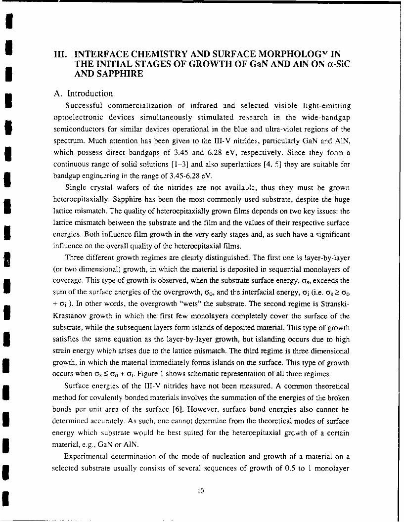
Three different growth regimes are clearly distinguished. The first one is layer-by-layer
(or two dimensional) growth, in which the material is deposited in sequential monolayers ofcoverage. This type of growth is observed, when the substrate surface energy, as, exceeds the
sum of the surface energies of the overgrowth, yo, and tl-e interfacial energy, (Ti (i.e. ys -> (o+ Ti ). In other words, the overgrowth "wets" the substrate. The second regime is Stranski-
Krastanov growth in which the first few monolayers completely cover the surface of the
substrate, while the subsequent layers form islands of deposited material. This type of growth
satisfies the same equation as the layer-by-layer growth, but islanding occurs due to highstrain energy which arises due to the lattice mismatch. The third regime is three dimensional
growth, in which the material immediately forms islands on the surface. This type of growthoccurs when Ts - ao + a. Figure 1 shows schematic representation of all three regimes.
Surface energies of the III-V nitrides have not been measured. A common theoretical
method for covalently bonded materials involves the summation of the energies of the brokenbonds per unit area of the surface [6]. However, surface bond energies also cannot be
determined accurately. As such, one cannot determine from the theoretical modes of surface
energy which substrate would be best suited for the heteroepitaxial grcwth of a certain
material, e.g., GaN or AIN.Experimental determination of the mode of nucleation and growth of a material on a
selected substrate usually consists of several sequences of growth of 0.5 to 1 monolayer
10

II
Ia
II
Figure I Schematic presentation of the three growth regimes: (a) Layer-by-Laver. N
Stranski-Krastanov, (c) 3-Dimensional.
i of material and analysis of the interface region either by Auger spectroscopy or XPS. The
growth steps are repeated until a total of five to ten monolayers have been grown. Such anexperiment is built on the fact. that electrons of a well defined energy travel in solids a
I certain distance without loosing their energy. This distance is called the escape depth. When
they pass through a material, the flux of these electrons decreases exponentially. Since lowenergy electrons (a few 1IM eV) have a very short escape depth (usually in the order of a fewmonolayers), they are a sensitive measuring tool for the characterization of very thin layers.If the substrate is excited with high energy electrons (as in Auger studies) or photons AXPS
characteristic electrons. one can consider the substrate as a source of an electron flux 1o. If a
fsI
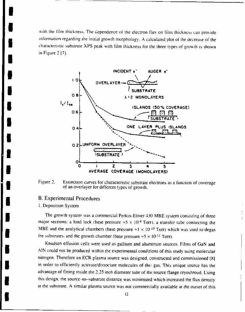
I
I with the film thickness. The dependence of the electron flux on film thickness can provideinfomiation regarding the initial growth morphology. A calculated plot of the decrease of thecharacteristic substrate XPS peak with film thickness for the three types of growth is shownin Figure 2 [7].I
u INCIDENT e- AUGER e-
OVERLAYER-
SUBSTRATE0.8- X,2 MONOLAYERS
I Is/120 a ISLANDS (50% COVERAGE)
0 6*-...L< rSUBSTRATE
04- ONE LAYER PLUS ISLANDS
02 _UNIFORM OVERLAYER 'e-
i )SUBSTRATE) "0 i I _ __ _
0 I 2 3 4 5AVERAGE COVERAGE (MONOLAYERS)
Figure 2. Extinction curves for characteristic substrate electrons as a function of coverageof an overlaver for different types of growth.
B. Experimental Procedures1. Deposition System
The growth system was a commercial Perkin-Elmer 430 MBE system consisting of threemajor sections: a load lock (base pressure -5 x 10⁻⁸ Torr), a transfer tube connecting theMBE and the analytical chambers (base pressure =1 x 10⁻¹⁰ Torr) which was used to degasthe substrates, and the growth chamber (base pressure -5 x 10-11 Torr).
Knudsen effusion cells were used as gallium and aluminum sources. Films of GaN and5 AIN could not be produced within the experimental conditions of this study using molecularnitrogen. Therefore an ECR plasma source was designed, constructed and commissioned 181
Sin order to efficiently activate/dissociate molecules of this gas. This unique source has theadvantage of fitting inside the 2.25 inch diameter tube of the source flange cryoshroud. Usingthis design, the source-to--substrate distance was minimized which increased the flux densityat the substrate. A similar plasma source was not commercially available at the outset of this
* 12

U
I effort. Some important parameters of the ECR source are given in the Table I.Ultra-high-purity nitrogen, further purified by a chemical purifier, was used as the source gas.3 The flow rate was regulated by a variable UHV compatible leak valve and was normally-5 sccm which resulted in a process charnber pressure of l x 104 Torr.I
Table I. Some parameters of the NCSU-ECR nitrogen plasma source.
Overall source diameter 57 mmPlasma diameter 23 mmMicrowave frequency 2.45GHzMicrowave power 0-100 WPeak magnetic flux 1.05 kGNitrogen ion current density at 50 W•at the source -1 mAcro- 2
i at the substrate 150-200 gtAcm - 2
Start pressure I x 10- 4 TorrMinimum operation pressure I x 10-5 TorrI
2. Film Growth
Growth studies were conducted on (0001)-oriented ax(6H)-SiC and the basal plane of
epitaxial quality sapphire wafers, both of which have a hexagonal structure. All substrateswere chemically cleaned to remove organic and metallic contaminants and mounted on a
standard 3 inch molybdenum block with indium which provided both good adherence and
3 thermal contact.
The substrates underwent an initial low temperature (=70'C) outgasing in the load lockI followed by slow heating in the transfer tube to a maximum of 700'C with a dwell time of
30 min at this temperature. After cooling, the samples were introduced into the growth
chamber and examined by reflection high energy electron diffraction (RHEED) using a
10 kV beam. The resulting RHEED patterns on both the ox-SiC and sapphire substrates
showed Kikuchi lines, indicative of a good crystalline quality.
Prior to growth, the substrates were heated to the desired deposition temperature andsubsequently exposed to a flux of plasma activated nitrogen species for about 5 min.3 Following the stabilization of temperatures and fluxes, a thin layer of GaN or AIN was
grown. The growth conditions are summarized in Table II. After the growth was completed.5 the gallium or aluminum cell and the substrate were cooled, while the nitrogen sourceremained active until the substrate temperature was below 400'C. One set of experimentswas conducted using photo enhancement, where a 500 W Hg lamp was used to irradiate the
13
I
I_ samples during the growth. The XPS results of this study were compared with those
described from the unirradiated sample.
n Table II. Growth conditions.
Nitrogen pressure I x 10-4 TorrMicrowave power 50 WGallium temperature 9000CAluminum temperature 11200CSubstrate temperature 6000C
I Thickness grown/deposition 0.2 - 0.5 nmNumber of deposition cycles 6 - 7
- Total number of monolayers grown 5 - 12
5 3. XPS Analysis
XPS (X-ray photoelectron spectroscopy) was performed on the cleaned substrates prior to
deposition and on the grown films after each deposition step. Samples were transferred from
MBE growth chamber to the analytical chamber under UHV conditions. XPS spectra were
obtained with a Riber Mg/Al X-ray source and a Riber MAC II cylindrical electron analyzer.
3 Spectral data were acquired by an IBM PC-AT running software developed at NCSU.For the study of the AIN growth, Mg Kot X-rays (1253.6 eV) were used to obtain spectra.
i For GaN growth, both the Mg and Al (1486.6 eV) anodes were used. The reason for
alternating the X-ray sources for the examination of GaN was due to the fact that the Ga3 Auger electron emission occupies a large region of the spectrum between 0 and 1000 eV, and
covers up certain XPS photoernission peaks of interest. The change of the X-ray energy shifts
the Auger emission lines on an intensity vs. binding energy plot for the change in the energy
of the X-ray photons, while the positions of the XPS photopeaks remains the same. The effect
of changing the energy of X-rays is illustrated in Figure 3. Figure 3(a) is a wide-energy scan
survey spectrum of GaN on sapphire obtained with the Mg X-ray anode, showing both
substrate and film photopeaks and the GaLMM Auger emission cluster, which covers about a
3 250 eV wide band of the spectrum, from 150-400 eV. Figure 3(b) is a similar survey
spectrum of GaN on SiC using the Al anode; this spectrum shows that the Ga Auger emission
has been shifted by an amount equal to the energy difference between the two sources
(233 eV). Owing to the positions of the Ga Auger emission, the Mg anode was used for
examining the Ols and Nis photopeaks, while the Al anode was used for examining the Ci1,
Si2s, Al 2p and Ga3d peaks.
For the study of GaN, the Si2, photopeak at 153 eV was used, rather than the more
commonly used Si2p peak, again because of interference from Ga emission. The Ga3p peak at
14I

I
1 107 eV lies very close to Si2p at 103 eV, and overwhelms the Si 2p emission, as the Ga signal
increases with the thickness of GaN film. The Si 2s peak is also near another Ga photopeak
3 (Ga3s at 160 eV) but is located farther from the nearby Ga peak than the Si2p peak is from its
Ga neighbor. No switching of the anodes was necessary for the examination of AIN films. All3 photo-peaks of interest are well resolved on both substrates with the Mg anode, as can be
seen in Figures 4 (a) & (b), which show a broad energy scan of AIN on SiC and sapphire,
3 respectively.
(a)
Ga1
Ga3 Ga3d
I I II II gII II I I I~'I I~~u I * su I m I I 1 i* I II
1(XX) 900 800 700 600 500 400 300 200 100 0
I Binding Energy [eVI
IIGaLmNI
~Gar
~~Ga3, -
U I
, I Si,
1 2 1 'i ~CIS Ga.
5 I (X) 9(y) 800 7() 600 500 400 300 200 100 0
Binding Energy
Figure 3. XPS survey spectra of GaN films: (a) Sapphire substrate, Mg X-ray source. (b)SiC substrate, Al X-ray source.
15

I
KI i. N ,
I ":
O KI A .
3 0K A
I1000 S00 o 400 200
Binding Energy (6\')
i (b)
IN IS
L
S'2 S i p
IiS
ICIS
I1000 800 6 00 400 200 0
Binding Energy
(eV)
Figzure 4. XPS survey spectra of AIN films: (a) Sapphire substrate. (b) SiC substrate. Mgi X-ray source was used in both cases.
Electron escape depths were obtained from the universal curve of mean free path of
electrons vs. their energy.171 The escape depth is relatively insensitive to the material
traversed bv the electrons. Since XPS photoelectrons of C, Si2 s and Ols have considerably
3different binding energies. the energies of the escaped electrons differ as well. Since the
energy of an escaped electron equals the incident X-ray photon energy minus the electron

I
I binding energy, electrons with higher binding energy acquire less kinetic energy when being
excited with the same kind of X-rays. Switching anodes from Mg to Al has an effect on the
kinetic energy as well. The escape energies of selected photoelectrons and their respective
escape depths are summarized in Table III.ITable I1. Photoelectron energies and their escape depths.I
Ois Cis Si2s
Photon Energy leVi 1254 (Mg) 1487 (Al) 1487 (AI)Binding Energy [eVi 531 283 152Kinetic Energy leV] 723 1204 13353 Escape Depth [A] 12±1 18±1 18±1
Si 2 s and CIs peak intensities were monitored during the growth on SiC substrates and Ois
peak was examined during the growth on sapphire. The areas of the substrate peaks obtained
I after each deposition were calculated, compared to the areas of the peaks from the virgin
substrate, and finally plotted vs. thickness of deposited material. Results were compared with
a theoretical curve for layer-by-layer growth.
The binding energy' value of each of the XPS photopeaks was referenced to the peak
position, which was expected to be the most invariant. This procedure minimizes the effects
of the analyzer characteristics and specimen charging. For the films grown on SiC, the Cis
peak was set at the typical value for SiC of 283.0 eV[9-1 I]. The other peaks were referenced
3 to that value. For the films grown on sapphire substrates, the Nis values of 397.0 for GaN
[11, 121 and 397.3 for AIN [ 11, 121 were used as reference positions. For the clean sapphire
substrates, prior to deposition, the photopeaks were referenced to the average value for Ols
observed during the remainder of the deposition.
C. Results and Discussion1. Growth Morphology: GaN
Figures 5 and 6 show plots of relative substrate peak intensities vs. film thickness
obtained during the growth of GaN both without (Fig. 5) and with (Fig. 6) UV treatment
during growth. Both figures also contain theoretical curves representing layer-by-layer
growth calculated at two escape depths, 12 (Cls,Si 2s) and 18 (Ols) A. The two curves
correspond to the growth on SiC and sapphire. respectively.
17

1 o- - Carbon
0.6-
0.0 G
I0 2 4 6 8 10GaN Thickness (A)
IFigure 5. Change of XPS photoelectron intensity during growth of GaN on cd(6H)-SiCand sapphire.
I0.8 Ter-
0.6-
0.4 .. ..... ...... ..... ...... ..... ...................... ...............
0.2 --..
I ~ ~~~~~~0.0 _ _ _ _ _ _ _ _ _ _ _ _ _ _ _
0 24 6 813 GaN Thickness (A)
Figure 6. Change of XPS photoelectron intensity during UV-enhanced growth of GaN on3 ut(6H)-SiC and sapphire.
18

I
I The plots in Figure 5 show that the substrate peak intensity diminishes initially faster forthe growth of GaN on SiC than on sapphire (compare Ols to Cjs and Si2p signals). This ismost likely due both to a faster initial nucleation process on SiC, and to the formation of athin silicon nitride layer at the interface (see below). This reasoning also agrees with thebehavior of the Ols signal. This signal decreases rapidly, once initial nucleation occurs, andwith the same slope as the Si-p and Cls signals at the very beginning of the growth.Furthermore, an earlier study in the authors' laboratory of the growth rate of GaN on
different substrates did not indicate a substantial difference between the growth rates on SiCand sapphire within experimental conditions. The growth rate was controlled by the Gaarrival rate rather than by any other factors.
Similar behavior for the change in the intensity of the Si2s and Cjs photoemission wasanticipated, since they originate from the same SiC substrate. However, this was notobserved. As shown in Figure 2, the Cls peak intensity shows a faster initial drop and alsosaturates at a lower value. This can also be explained by the formation of a thin layer ofsilicon nitride. Since the Si-face of the SiC substrates was used, a silicon nitride layer formedon the surface during exposure to the reactive N species prior to film deposition. This
resulted in burying the carbon layer more deeply under the Si. The difference in the initialintensity drop approximately corresponds to the formation of one monolayer of siliconnitride.
All three curves assume a more gradual behavior after the initial rapid drop. The slopes of3 the Cjs and Si2 s signals in this region are considerably lower than the slope of thecorresponding theoretical curve, which indicates an early saturation, while the slope of the3 Ols signal exhibits a closer match to its theoretical curve. However, none of the experimentalcurves resembles the corresponding calculated curves for layer-by-layer growth.
The growth of GaN on sapphire appears to follow a Stranski-Krastanov mode while the
growth on SiC shows some characteristics of three dimensional growth, although one wouldexpect from the lattice mismatch a smoother growth on SiC than on sapphire. At present it isunclear whether or not this is due to the formation of a thin interfacial layer of silicon nitride.
Figure 6 shows the ,xtinction curves of the substrate elements during UV-enhanced3 growth of GaN. In this case the substrate peak intensities show the same tendency to level offas they did in the first experiment, but slightly later in the growth process. In both cases3 however, the experimental curves drop more rapidly and subsequently show a tendency tolevel off before they reach zero, which is in contrast to the corresponding theoretical curvesfor layer-by-layer growth. As mentioned above, these curve shapes suggest island formation,
either complete three-dimensional growth or Stranski-Krastanov growth. In the case of GaNgrowth without UV enhancement (Fig. 5), growth appears to be three-dimensional on SiC,and to follow a Stranski-Krastanov mode on sapphire with the formation of one monolayer.
'9

I
I In the case of UV-enhanced growth, the extinction curves for both SiC and sapphire are allsimilar, and indicate Stranski-Krastanov growth after the formation of 2 or 3 monolayers.3 Additionally, the results shown in Figure 10 reveal less evidence of silicon nitride formationthan is indicated in Figure 5.
I 2. Growth Morphology: AIN
Figure 7 shows the change in XPS substrate peak intensities acquired during the growthof AIN. In this case, the experimental data resemble the corresponding theoretical curvesmore closely. This indicates that AIN grows layer-by-layer. This is in agreement with severalreports which indicate that GaN films are affected beneficially when grown on an AIN bufferlayer previously deposited on sapphire. Figure 8 shows the extinction curves obtained andcalculated for UV-enhanced AIN growth. Here the experimental data indicate thedevelopment of island growth after 1 or 2 monolayers had formed. There is also more3 evidence of silicon nitride formation, as the Cls signal drops off much more rapidly andsaturates at a lower value than does the Si. As is the case with UV-enhanced growth of GaN5 (Fig. 6), the overall behavior of the two substrates appears to be similar.
" *,A-A. Silicon
"-.... .' L,,._~ .... ,,[ .D Oxygen
I0.8 Theory-C, Si
~...... .... ,
2 0.6
0.4
0.2
IJ.0
) 2 4 6 8 10 12 14 16
AIN Thickness (A)
3 Figure 7. Change of XPS photoelectron intensity during growth of AIN on ot(6H)-SiC andsapphire.
!20

I 1.0 Carbon
-.A- Silicon0" Oxygen
0.8 -- Theory-C, SiTheorv-O
0.6
CI ,0.4 -
3 0.2
0 5 10 15 20 25 30
* AIN Thickness (A)
Figure 8. Change of XPS photoelectron intensity during UV-enhanced growth of AIN onio(6H)-SiC and sapphire.
3. Interface Chemistry: GaN
3 XPS was also used to characterize the chemical state of the substrates, interfaces and the
growing films during the MBE deposition of GaN and AIN. Analysis of the cleaned3 substrates prior to deposition revealed the presence of very small amounts of carbon and
oxygen surface contamination. The binding energy values obtained with reference to a
particular peak for the growth series of GaN and AIN on sapphire and on a(6H)-SiC are
listed in Tables IV. V, VI and VII.
In the case of non-UV-enhanced GaN growth (Table IV), the only XPS photopeak to
show any significant binding energy shift is the Al2p emission from the sapphire substrate.
The slight shift (0.6 cV) may indicate that some Al-N bonding is taking place during GaN3 deposition, and the proportion of AI-N bonds increases with increasing coverage until the
substrate is completely covered.3 The A12p signal shows somewhat different behavior during the UV-enhanced growth
(Table V). With the first deposition, the binding energy of the Al emission drops more than 1
eV and then gradually reaches a value similar to that in the first experiment. At the present
time the reasons for this behavior are not well understood. The Ga3d signal also shows a
slight shift in the higher binding energy direction. The relatively low initial binding energy
value for Ga is closer to the published values for elemental Ga than to GaN. This value
21

I
I subsequently shifts to a higher value during deposition. It is possible that less of the Ga had
reacted to form GaN in the early stages of the experiment, even though XPS peak-area
3 calculations for Ga/N stoichiometry revealed a higher Ga/N ratio (of total Ga and N
emission) from the first growth steps than from subsequent depositions.ITable IV. Binding energies of XPS photoelectrons measured during the GaN3 growth on sapphire and (6H)-SIC.
Growth Step 0 1 2 3 4 5 6On sapphire:
Al2p 74.0 73.8 73.6 73.4 73.7 73.4 73.4Ols 531.0* 531.3 531.1 531.0 531.2 531.0 530.9Ga3d - 19.3 19.2 19.0 19.2 19.1 19.2NIs* - 397.0 397.0 397.0 397.0 397.0 397.0
On ox(6H)-SiC:Si2s 152.1 152.2 152.2 152.2 152.2 152.2 152.2CIS* 283.0 283.0 283.0 283.0 283.0 283.0 283.0Ga3d - 19.9 19.9 20.0 19.9 20.0 20.0Nis 397.7 397.6 397.7 397.5 397.6 397.7II
3 * Values set as reference.
ITable V. Binding energies of XPS photoelectrons measured during the
UV-er hanced GaN growth on sapphire and ox(6H)-SiC.
I Growth Step 0 1 2 3 4 5 6On sapphire:
Al 2p 74.0 72.7 72.8 73.2 73.., 73.2 73.6OIs 531.0* 530.8 531.0 531.1 531.0 531.0 531.0Ga3d - 18.5 18.4 18.9 18.8 18.9 19.0Nis* - 397.2 397.2 397.2 397.2 397.2 397.2
On x(6H)-SiC:Si 2p 100.9 101.0 101.0 101.1 101.1 101.0 101.1Cis 283.0 283.0 283.0 283.0 283.0 283.0 283.0Ga3d - 20.1 20.1 20.1 20.1 19.9 19.8NIs- 398.0 397.9 397.9 397.8 397.7 397.5
3 Values set as relcrences; NSP = no significant peak.
I

Table VI. Binding energies of XPS photoelectrons measured during
the AIN growth on sapphire and o (6H)-SiC.
Growth Step 0 1 2 3 4 5 6On sapphire:
A12p 75.0 75.0 75.0 74.8 74.5 74.2 74.1Ohs 532.0* 532.2 532.1 532.0 531.9 531.8 531.8NIS* - 397.3 397.3 397.3 397.3 397.3 397.3
On o(x6H)-SiC:Si2p 100.9 101.0 101.0 101.1 101.1 101.0 101.1Cis 283.0 283.0 283.0 283.0 283.0 283.0 283.0A12p NSP NSP NSP 74.0 74.0 74.1Nis 397.6 397.6 397.5 397.3 397.3 397.4
Values set as references, NSP = no significant peak.
Table VII. Binding energies of XPS phot-',ec roi.3 measured during
UV-enhanced AIN gro, ., un sapphire and at(6H)-SiC.
Growth Step 0 1 2 - 4 5 6 7On sapphire:
Al2p 74.9 74.9 74.6 74.6 74.4 74.3 74.1 74.0Os 531.9* 532.2 532.0 531.9 531.8 532.0 531.7 531.7Nis* 397.3 397.3 397.3 397.3 397.3 397.3 397.3
On ct(6H)-SiC:Si 2p 100.7 100.8 100.9 101.0 101.0 100.9 101.2 101.0Cis 283.0 283.0 283.0 283.0 283.0 283.0 283.0 283.0AI2p - 73.4 73.8 73.8 73.8 73.8 73.8 74.0Nis - 397.1 397.2 397.2 397.2 397.1 397.2 397.4
* Values set as references.
4. Interface Chemistry: AIN
The binding energy values of the Al2p emission during AIN growth on sapphire (Tables
VI and VII) show trends similar to those seen in GaN growth. In this respect there is no
difference caused by the application of UV excitation during growth. Additionally. in the
case of UV-enhanced growth of AIN on SiC the Al2p signal behaves in a manner similar to
that of Ga3d during UV-enhanced growth. The slight shift of the Al2p peak from a lower
binding energy value to a higher one corresponding to AIN is an indication that AI-N bonding
i is not complete in the earliest stages of deposition.
23

I
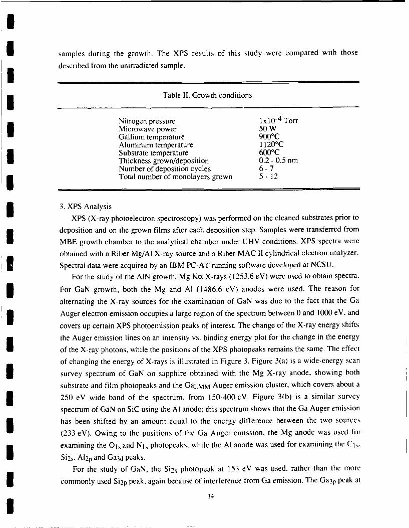
I The sequence of Si2p peaks acquired between deposition steps during the growth of AINon o(6H)-SiC is shown in Figure 9. The initial Si-p signal from the bare substrate was a
symmetrical peak characteristic of clean SiC. With the first ',IN growth step, significantshouldering of the peak appeared on the high binding energy side, indicating the presence of3 a more highly oxidized state of the silicon. This shoulder persisted throughout the filmdeposition process and remained as the SiC component and the overall Si intensitydiminished with film growth. Gaussian curve fitting analysis was applied to the most intense
shouldered peak, obtained at the first growth step, to resolve the position of the high binding
energy component. The results of curve fitting are shown in Figure 10.
By means of Gaussian curve fitting, the high binding energy shouldering was found to beprimarily due to a single component shifted 1.4 eV from the mai SiC peak. This component3 has been attributed to the formation of silicon nitride during the initial stages of AIN growth.
This behavior shows that the Si-face of SiC initially undergoes nitridation.m The UV-enhanced growth of AIN on SiC exhibited very similar behavior. Shouldering of
the Si2p peak was again quite apparent, and curve fitting of the shouldered peaks revealed thesame silicon nitride component shifted 1.4 eV from the SiC peak. The results of this curve
fitting for UV-enhanced growth are shown in Figure 11.A similar conclusion could not be made for the growth of GaN on SiC, although there isIlittle reason to expect that in this case a completely different chemistry initially occurred at
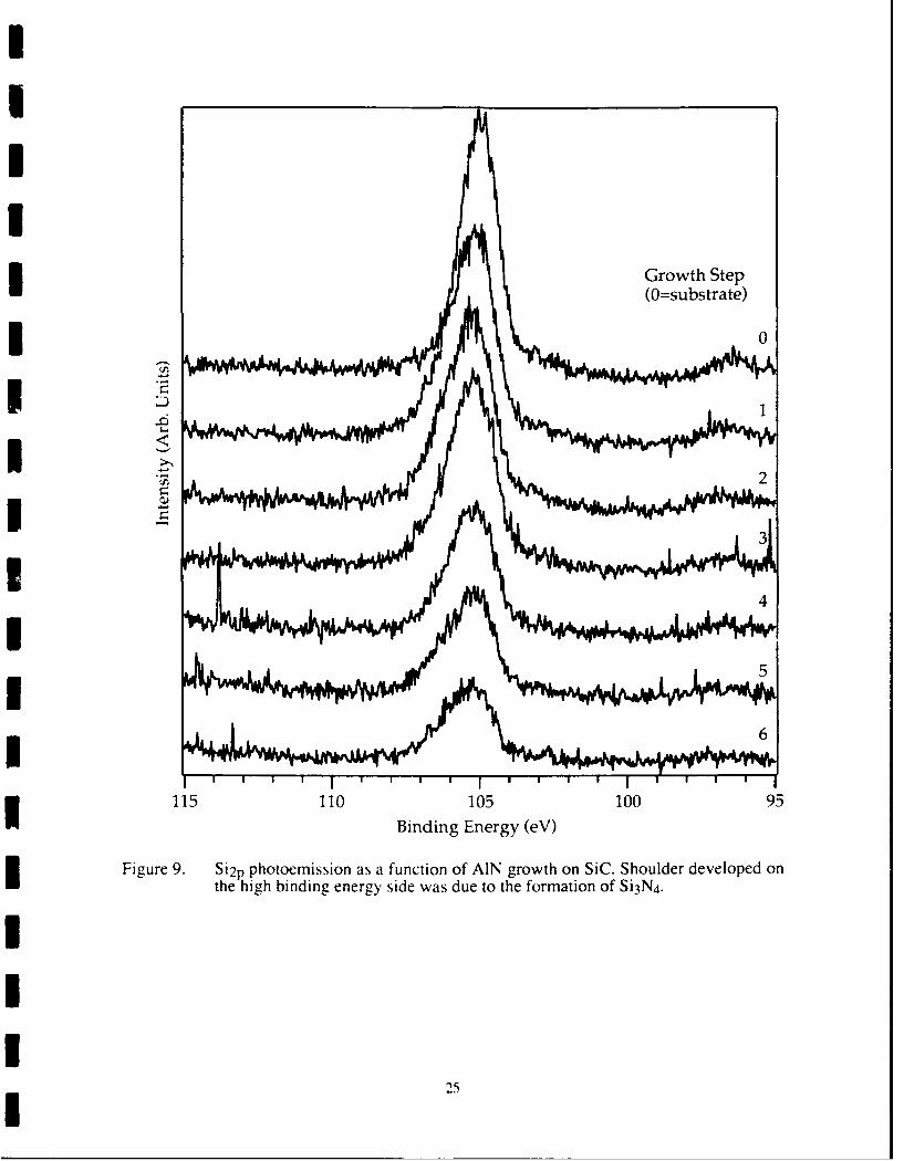
tti, interface. The sequence of Si2s peaks acquired between deposition steps during growth ofGaN on ox(6H)-SiC is shown in Figure 12. However, the shouldering effect was not apparent,
since Si spectra obtained during the growth of GaN show lower peak intensities and a poorersignal-to-noise ratio than the spectra obtained for AIN. The close proximity of the Ga3s peak
on the high energy side, as shown in Figure 3, could have obscured the evidence of the
silicon nitride formation as well.
The film elements Ga, Al, and N exhibited no significant changes in chemistry, except for
the slight shift of the Al-p peak from AIN growth on sapphire as the A120 3 gave way tr) AIN.
Thus the XPS anal\,I, indicates that no significant chemical reactions occurred between thegrowing films and the ubstrates other than the formation of small amounts of interfacial
SiON 4 during the initial ,tai!es of growth on SiC.
24
Growth Step(0=substrate)
I0
- 2
I3
6
115 110 105 100 95
Binding Energy (eV)
Figure 9. Si2p photoemission as a function of AIN growth on SiC. Shoulder developed onthe high binding energy side was due to the formation of Si 3N4.
25

II SiC
101.0 eV
U.-.Overall Fit
E-
Si3N4102.4 eV
X
110 105 100 95
Binding Energy (eV)Figure 10. Gaussian curvefit of Si 2 p photoemission from AIN deposited on a-SiC,
showing component attributed to Si 3N4 shifted 1.4 eV from SiC peak.
SiC100.8 eV
IZ
Overall Fit
€..M
102.2 e
110 105 100 95
Binding Energy (eV)
Figure 11. Gaussian curvefit of Si 2p photoemission from UV-enhanced deposition of AIN
on ot-SiC, showing Si 3N4 component.
26
II
Growth Step(O=substrate)
I2I3I4I5
,6I-
160 155 150 145Binding Energy (eV)
Figure 12. Si2s photoemission as a function of GaN growth on SiC.
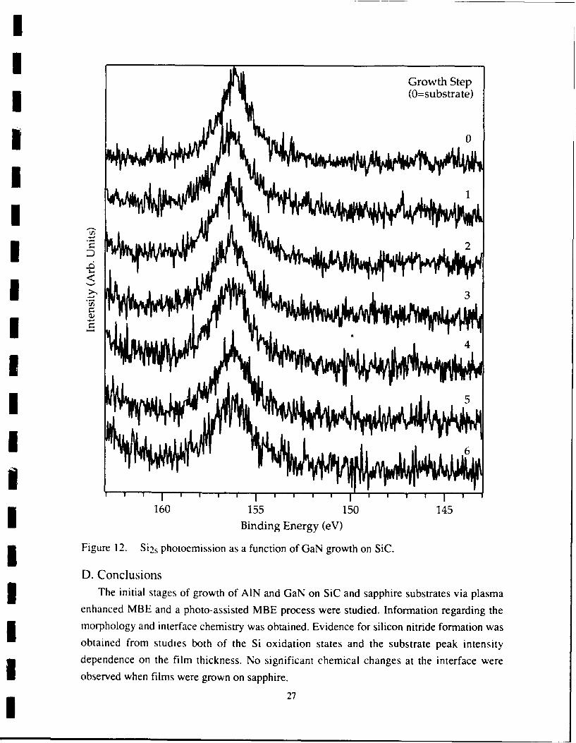
D. ConclusionsThe initial stages of growth of AIN and GaN on SiC and sapphire substrates via plasma
enhanced MBE and a photo-assisted MBE process were studied. Information regarding themorphology and interface chemistry was obtained. Evidence for silicon nitride formation was
obtained from studies both of the Si oxidation states and the substrate peak intensitydependence on the film thickness. No significant chemical changes at the interface were
observed when films were grown on sapphire.
27

A faster GaN nucleation was observed on SIC, while AIN apparently nucleated on both
substrates equally well.
The growth of GaN on sapphire appeared to occur via the Stranski-Krastanov mode,
while the growth on SiC showed some characteristics of three dimensional growth. At
present, it is unclear whether or not this latter result is solely due to formation of thin
interfacial layer of Si3N 4 .
The study of AIN showed that it grows layer-by-layer on both substrates. The application
of UV radiation during the growth did not produce any significant changes.
E. Future Research PlansThe deposition of AIN and GaN and layered structures of these materials via GSMBE
will be continued. Since the main goals are the improvement of the quality of materials, and
growth of p-type GaN and AIN the short term research will be devoted to the production of
smooth layers of both materials and their solid solutions. Mg will be used as the dopant for
both compounds. A Hg UV light source will be to be used in the doping studies. Having
achieved the quality and desired electrical properties, all efforts will be focused toward the
growth of structures for simple optoelectronic devices.
F. References
1. M. R. H. Khan, Y. Koide, H. Itoh, N. Sawaki and I. Akasaki, Solid State. Comm. 60,509 (1986).
2. S. Yoshida, S. Misawa and S. Gonda, J. Appl. Phys. 53, 5844 (1982).3. Y. Koide, H. Itoh, M. R. H. Khan, K. Hiramatu, N. Sawaki and I Akasaki, J. Appl.
Phys. 61. 4540 (1987).4. Z. Sitar, M. J. Paisley, B. Yan, J. Ruan, J. W. Choyke, and R. F. Davis, J. Vac. Sci.Technol. B 8, 316 (1990).
5. Z. Sitar, M. J. Paisley, B. Yan, J. Ruan, J. W. Choyke, and R. F. Davis, Thin SolidFilms, 200, 311 (1991).
6 A.W. Adamson, Physical Chenistry of Surfaces, 5th ed. John Wiley and Sons, Inc.,N.Y., 1990.
7. L.C. Feldman and J.W. Mayer, Fundamentals of Surface and Thin Film Analysis.North-Holland, N.Y.
8. Z. Sitar, M. J. Paisley, D. K. Smith, and R. F. Davis, Rev. Sci. Instr. 61, 2407 (1990).9. F. Bozso, L. Muehlhoff, M. Trenary, W.J. Choyke, and J.T. Yates, Jr., J. Vac. Sci.
Technol. A 2, 1271 (1984).10. P.A. Taylor, M. Bozack, W.J. Choyke, and J.T. Yates, Jr., J. Appl. Phys. 65, 1099
(1989).11. NIST X-Ray Photoelectron Spectroscopy Database, version 1.0, NIST Standard
Reference Database 20. National Institute of Standards and Technology, GaithersburL.MD, 1989.12. J. Hedman and N. Mdrtensson, Ph\'sica Scripta 22, 176 (1980).
28

I
IV. GAS-SOURCE MOLECULAR BEAM EPITAXY OF BORONNITRIDE AND GALLIUM NITRIDE
A. Introduction1. Boron Nitride
Boron nitride has long been known for its desirable properties as a highly insulating as
well as a chemically and thermally stable material. The cubic phase of boron nitride was first
reported by Wentorf,[ 1] who produced it in a high pressure apparatus. This investigator also
conducted the initial measurements regarding the semiconducting properties of this material.
It has been used since then primarily for its high hardness in applications such as grinding
and polishing. The cubic phase of BN is actually the zinc blende structure or, in space group
notation, F43m (Hermann-Mauguin) or T 2 (Schienflies). Boron nitride is very similar to
carbon in that both exist in hexagonal, wurtzitic, and cubic forms and many of the properties
in each of the phases are strikingly similar. For example, both diamond and c-BN are
metastable under the conditions currently used for growth of thin films. The primary
difference is that hexagonal boron nitride is an insulator and hexagonal carbon is a conductor.
Interest in the cubic polymorph of BN as a semiconductor material has received much
interest recently as a possible substrate for the deposition of diamond, due to the similar
lattice parameters (Aao=1.34%) and its wider bandgap which is in the range of 5.8-6.5 eV.[2-
4] Potential applications which would make use of the very wide bandgap of c-BN include
optical devices for the vacuum UV (X-200 nm) and high-power electronic devices. For a
complete listing of materials-related properties of c-BN see Landolt-Bornstein:Numerical
Data and Functional Relationships in Science and Technology, Series III, Vols. 17 and 23, or
Ref. [5] (which also includes a side-by-side comparison of properties of c-BN with diamond).
Several approaches have been employed in the attempt to grow thin films of cubic boron
nitride (c-BN). These include reactive diode[6] and rf sputtering,[7] ion implantation,[8, 9]
plasma CVD,[10-121 microwave plasma CVD,[13, 14] and ion plating tec'niques.[15-181
These attempts were successful in producing polycrystalline films of c-BN, predominantly of
a mixed nature with both cubic and other phases present and of extremely fine grain size. It
appears that most researchers succeeded in the deposition of c-BN if the technique included
the input of additional energy from energetic ions during the deposition process.
Research in the present program using microwave plasma CVD to deposit c-BN films and
conducted in conjunction with ASTeX, Inc., has been described in the paper submitted to
Kobe Research and Development. A preprint of this paper is included in this report as
Appendix I. This study has attempted to use the energetic plasma conditions of a microwave
ECR source to provide that important additional energy. The previous progress report of
June, 1991, indicated that tle resulting films were amorphous with cubic character. In
29

discussing future research plans in that report, mention was made of the use of a UV light
source to provide additional energy to the gro,,h processes. This process route has sincebegun to be investigated for the growth of c-BN. However, since photo-enhancement ofgYrowth processes is a relatively new field, this field will be briefly reviewed in the following
section.
2. Gallium NitrideGallium n-tride (GaN) is currently known to occur in two different tetrahedrally-
coordinated crystal structures. The best characterized polymorph is wurtzitic GaN which, inspace group notation, is P63mc (Hermann-Mauguin) or C4, (Schbenflies) or B4
(Strukturbericht). It has the lattice parameters of a=0.3190 nm and c=0.5189 nm (Note thatla=1.627 is near the ideal ratio of 1.633 for hexagonal unit cells.).[ 191 The more recentlydiscovered cubic polymorph of GaN is actually the zinc blende structure or, in space group
notation, F43m (Hermann-Mauguin) or T (Schoenflies) or B3 (Strukturbericht) with a lattice
parameter of 0.451 nm.The cubic polymorph has properties only slightly different from wurtzite, due to the fact
that the bonding environments are similar. Indeed, the two structures differ only in the
stacking of essentially identical tetrahedral units.[20] Thus, it is expected that the properties
of c-GaN would be very similar to that of w-GaN. Since w-GaN is far better characterized, itsproperties will be used in the discussion of the material in general.
Wurtzitic GaN is a wide bandgap (3.45 eV at 300K, or 3.28 eV for c-GaN)1211 III-V
compound semiconductor. The large direct bandgap and high electron drift velocity of GaNare important properties in the performance of short wavelength optical devices and highpower microwave devices. Immediate applications that would be greatly enhanced by the
availability of GaN and/or AlxGalxN devices include threat warning systems (based on the
ultraviolet IUV) emission from the exhaust plumes and supersonic bow shock of missiles)
and radar systems (which require high power microwave generation). Important future
applications for devices produced from these materials include blue and ultravioletsemiconductor lasers, blue light emitting diodes (LEDs) and high temperature electronic
devices.
3. Photo-Enhanced Growth
Unfortunately, the study of photochemistry in the solid state has progressed slowly,especially in comparison to solutions and gases. Fleischauer points out in his review of solidstate photochemistryl221 that this is due to the complexities of the analysis when compared tosolutions and gases. Readers are referred to Fleischauer's review for information on photo-
chemical processes, though it is strongly slanted toward examples in research on metal
30
I
complexes. In the sections that follow, only those processes which might have an impact on
growth phenomena are covered.
Photo-enhanced growth techniques are generally applications of photochemistry to the
growth processes, with the possible exception of purely thermal effects. Use of
I photochemical processes for growth of thin films is a relatively recent development,[23] and,
as applied in MBE deposition, has been characterized as being in its infancy.[24] Thus it is
3 not surprising that extensive searches of the thin film semiconductor growth literature have
shown only limited application of the potential photochemical effects which can be exploited.
For this reason, the next sections will describe the types of photo-enhancement effects that
can occur.
Current literature on the photo-enhanced growth of thin films can be classed into five
basic categories: thermal effects (both equilibrium and non-equilibrium), enhanced atom
mobility, photolytic and enhanced pyrolytic decomposition effects, dopant activation, and
other photochemical effects. In a number of cases these effects are thought to occur in
combination.[25, 26) The first four subsections of this report will be limited to situations
I where these photochemical effects have been explicitly observed during thin film growth.
The fifth section will discuss other photochemical processes which have not been explicitly
observed in thin film growth, but which might be utilized to enhance the processes of thin
film deposition.
Thtrmai Effects. Purely thermal effects are those attributed to heating of the substrate by
absorption of the incident photons. This may take the form of near-equilibrium heating of
substrates by lamps,[26-281 or involve the use of lasers and is categorized either by
3 plasmas[29, 30] or extreme localized heating and/or melting of the surface.[28] The heating
effects exploited with lamps of various types are used for technological reasons (e.g., high
heating rates,[28] low thermal mass, or materials service compatibility[27]) rather than
specific effects on the growth processes. Laser thermal processing is used especially where
the localized nature of the heating can be exploited.[28]
Enhanced Atom Mobility. Enhancement of the mobility of atom species on the growth
surface is a fairly new but rapidly increasing application of photo-enhanced growth.
5 Illumination of species on the growing surface can produce activated species which increases
the rate of surface diffusion and thus improve crystal quality,[31-33] even to the point of
crossing the transition from polycrystalline to single crystal growth.[26] Though less often
observed, this phenomenon can also occur in the bulk (i.e., not during growth).[34] This
5 enhanced diffusion phenomenon has also been observed to cause ordering in vacancy-donor
complexes in CdTe.[35] A related phenomenon is the enhancement of desorption of certain
adsorbed species.[ 32-331
3'
I
I Photolvtic Decomposition. Photolytic decomposition or photo-enhanced pyrolytic
decomposition coupled with the use of metallorganic precursor compounds is the most
common use of photo-enhancement during deposition. By choosing the proper illuminatingwavelength(s) and precursor species the deposition will be enhanced or even selectively
controlled by the illumination of the substrate.[231 Light sources that have been used havebeen lasersJ231 disk-shaped plasmas,[251 or arc lamps.1261
Photolytic processes are not restricted to decomposition of metallorganic sources. For
example, photolytic decomposition as been observed in Ga2 vapor at relatively low energiesof =25,000 cm- 1 (3 eV or 400 nm).[361 These processes have also been used in thedeposition of such materials as amorphous Si[371 and AIN.[311 Two photon process
dissociation has also been observed for a number of cases,[381 which could be applicable in
I cases of laser illumination.While strictly not a decomposition reaction, a somewhat related phenomenon is the3 photo-excitation of atomic or molecular species. The energies and absorption cross-sections
for many common atoms and simple molecules are described in Photochemistry of Small3 Molecules by Hideo Okabe.[39] Such processes have been presumed to be a part of the
growth effects observed in deposition of ZnS from elemental sources.[32]Dopant Activation. An as-yet unexplained mechanism utilized in photo-assisted growth
processes has been dopant activation during photo-assisted MBE. This process wasdeveloped for substitutional doping in I-VI compound semiconductors in the Physics3 department at NCSU in the research group headed by Dr. Jan Schetzina.[40, 411 They haveachieved, among other things, hole concentrations (>2x1018 cm- 3) in p-type CdTe of -100x3 larger than conventional thermal equilibrium bulk methods.[42]
Photo-assisted dopant activation has since been observed in other systems. Yamazaki et
al.[23] achieved growth of Si with completely activated boron which produced carrierconcentrations of up to 1.5x 1020 cm-3 by UV irradiation. Subsequent fabrication of bipolar
transistor structures resulted in ideality factors of =1.0. Enhancement of dopant incorporation
was also observed by Fujita et al.1431 in growth of ZnSe. They reported enhancedincorporation of intentional and unintentional doping levels depending on the wavelengths of3 the illumination used. However, it is not clear whether the observed effect was electrical
activation of dopants present and/or enhanced incorporation of intentional/unintentional
3 dopant atoms.
A number of other photochemical effects have been observed which perhaps have not
been effectively applied to problems in thin film growth. These effects will be discussed in
this next section.
Other Photochemical Effects. As Giles et al.1401 pointed out in their paper describing the
photon-induced electrical activation of dopants, there are a large number of photochemical
3 2
I
effects which can occur during growth. In addition to the effects already discussed above,
they also listed modification of the electrical potential of the surface through the generation
of electron-hole pairs and photochemical changes in atomic bonding.Photo-generation of electron-hole pairs can be exploited to good effect by migration of
these generated carriers to the interface, where they become localized and break bonds. Onelong established (since mid-60's or before) application combines this effect with an
electrochemical cell to cause oxidation, etching or deposition in semiconductors.144] The
actual reaction that would occur being dependent upon carrier type and solution chemistry.An application of this effect which occurs entirely in the solid state (first observed in
1966) involves so-called "photodoping" which is the term applied to the photo-activated
diffusion of Ag in chalcogenide and some other glasses. Though there are differences in theproposed models regarding the diffusion of the Ag in the bulk, the consensus of opinion is
that the initial entry of the Ag into the glass is caused by photo-generated carriers diffusing to
the interface. [45-47]
A more thin film or vacuum deposition-related application of the same phenomenon is
described in the study of t'.- .,otochemistry and/or photocatalysis of molecules adsorbed
onto surfaces. The reacO r . referred to the excellent review of photocatalytic reactions on
semiconductors by VWolkenstein[48] for a more complete discussion of these effects which
also includes examples. One minor flaw in Wolkenstein's treatment pointed out byMorrison[49 1 is the use of the Fermi level as a dominant variable, since the Fermi level is
sensitive to so many variables.
An example from the photochemistry literature is the study made by Ho on thephotochemistry of NO adsorbed onto Si( I 11)7x7.[501 He found that adsorption of NO
increased the band bending occurring at the Si surface. Thus when the surface was
illuminated, holes were rapidly accelerated to the surface before electron-hole recombination
could occur, where the holes ruptured bonds causing the NO molecules to be desorbed and/or
dissociated. This is illustrated schematically in Figure 1.
Ho also described the case of Mo(CO) 6 adsorbed onto Si(I I 1)7x7, where the
photochemistry of the adsorbed species could be affected directly. However, he pointed outthat the photochemistry of adsorbed species need not be similar to that of the gas phase. A
weakly physisorbed species would have a very similar photochemistry to that of a gas phase
species. However, a more strongly physisorbed or even chemisorbed species would have a
dramatically different photochemical response. Indeed, Cowen et al.1511 described thephotochemistry of adsorbed species as "'strongly perturbed." They noted that the changes
could involve reaction inhibitions, enhancements, or even shifts in wavelength. For example,
Cowin and co-workers[511 reported the photo-fragmentation of C1t3Cl on Ni at 248 nm, a
wavelength that gas phase CH3CI does not absorb.
33

I
I Unmodified Si surface Si with NO adsorbed Si with NO adsorbed
onto the surface under illuminationI
Iq DifffusionS.....E...... ..... El ------ Ef -----..................... EJ
/ / // / ,EN /N /Acceleration Ex
(a) (b) (c)
I Figure 1. A schematic diagram of desorption of NO from Si surface due to the influence ofphoto-generated carriers (after Ho[47]). In (a) the normal Si surface, (b) NOadsorbed on the surface and increasing the band bending, and (c) photon createdholes accelerate to the surface, causing bond rupture and desorption.
3Examples from the thin film deposition literature include the photo-induced desorptionreported by Matsumura et al.[33] in the growth of ZnSxSel-x films. They did not determine ifit was electron-hole mediated or direct photon desorption. Additionally, Celii et al.1521
reported that UV laser irradiation suppressed the formation of diamond in filament-assisted
deposition. They determined that it was not a gas phase reaction, and speculated that the
irradiation somehow removed potential nucleation sites, since diamond crystals fromirradiated and unirradiated areas were otherwise similar in all respects.3 Photo-induced changes in bonding need not only result in desorption/adsorption or
dissociation. Much more subtle changes in bonding can be caused by illumination. Bicknell-
Tassius et a1[351 reported the preferential orientation of photoluminescence defects occurredduring photo-assisted MBE of CdTe. They postulated that vacancy-donor complexes were
aligned along preferred crystallographic directions due to the irradiation.
Other much more subtle bonding changes have been observed as well. Feenstra and
McGill[53] reported the dissociation of Zn-O defect pairs in GaP. They reported that these
defect pairs which form as Zn on a Ga-site and 0 on an adjacent P-site can be dissociated bypurely thermal means at 1000K. At lower temperatures (=500K), the reaction will proceedivia photoexcitation. They further reported that the defect pairs will reform, but at a larger
separation distance.The most unusual application of photon irradiation might well be the stimulation of a
change in crystalline structure. This process was coined the "photophase effect" by Alfimov
et al.1541 in 1984. They reported work by others on photophase changes includiig
34

I
condensation of gas phase molecules, crystallization of anthracene melts and a new
crystalline phase of anthracene. Fleischauer[221 also reported work by others involving x-ray
induced phase transformations in metal complexes.
Matsuda and Kikuchil[55] reported the first evidence of a photo-induced phase change in
a simple binary system. They examined samples in the As-As2S2 system, and formed the
new compound As 3S2. Though the new phase is unstable at room temperature, they found
that it was stable in the range of 150-190'C.
Conclusions on Photo-Enhancement. It is clear from the description and references given
above that photo-enhanced growth processes can be extremely complex. The dynamic nature
of these processes mean that without extensive study even simple predictions cannot be made
regarding which source/material systems would be candidates for particular forms of photo-
enhancement. However, it is also apparent from the examplzs cited that the advantages of
photo-enhancement can be extremely important in producing the desired properties for a5 given materials system. The difficulties in applying photo-enhancement are several, but the
advantages are unambiguous. These advantages may well be applied to the growth of c-BN3films. Documented in the following sections are the initial observations of the photophase
effect in BN growth.
SB. Experimental ProcedureThe primary deposition technique was GSMBE. Elemental boron and gallium were3 evaporated from effusion cells, and reactive nitrogen species were obtained by passing
molecular nitrogen through a compact electron cyclotron resonance (ECR) plasma source.
The growth system was a Perkin-Elmer 430 MBE system modified as described below. It
consisted of three major sections: a load lock (base pressure =5 x 10⁻⁸ Torr), a transfer tube
(base pressure -3 x 10- 1 ) Torr) which was used to degas the substrates, and the growth
I chamber (base pressure -1 x 10⁻¹( Torr). The growth chamber was equipped with four
standard 20 cc effusion cells and one high-temperature cell, the latter of which contained the5 B. All metals "ere contained in BN crucibles which were resistively heated either with Ta or
W alloy wire heaters The gallium cell was loaded with 50 g of 99.999 999% pure gallium.3 The special high temperature cell noted above was monitored using a W3%Re-W26%Re
thermocouple. An\ decomposition of the crucible at the elevated operating temperatures did
not affect the gro\, tth of the BN films. Prior to installation of the source, the BN crucible was
loaded with 3 g of 99.9999/ pure boron.
The more sinificant modification was the use of a compact ECR microwave glow-
discharge plasma to dissociate/activate the N-containing gas. This source was designed and
commissioned in an in-house effort by Dr. Zlatko Sitar.1561 This source has the advantages
I of fitting inside the nominal two-inch diameter tube of the source flange cryoshroud and thus
I 35

minimizes the source-to-substrate distance. As a result, the flux of activated/dissociated
species arriving at the substrate surface is increased. This source was attached in place of amore traditional effusion (or cracker) cell for the group V element. The nitrogen gas was
taken from a bottle of compressed UHP-grade nitrogen. purified by a metallorganic resin bedgettering material and subsequently regulated to the source by a variable leak valve.
Borazine (B3N 3H6 ) contained in a nitrogen carrier gas was also investigated for the
deposition of BN, as this chemical is a source for both boron and nitrogen. Borazine was also
chosen as a gas source in order to investigate both the activation of this material in the ECRplasma as well as attempt to determine if boron-nitrogen compounds provide a more suitable
precursor, since the B-N bond already exists in the material. This was done by placing the
borazine (which is liquid at STP) in a temperature controlled bubbler and passing nitrogen
gas through it which then passed into the ECR source.Substrate preparation involved a 30 min. exposure to UV which has been shown to
remove hydrocarbon contamination,[571 followed by a dilute acid etch to remove oxidelayers. In the case of Si, a solution of H20:HF (10:1) was used,[581 and for Cu, a solution ofH20:HC1 (10:1) was employed.[59] Subsequently, the substrates were mounted on a Mo
holder using either molten indium or silver paste. Silver paste was very important for the
copper substrates as they were extremely sensitive to oxidation and would oxidize heavily in
attempting to indium bond the substrates.
Samples were then loaded into a cryopumped load lock. After the initial evacuation, the
samples were loaded into the transfer tube where they were degassed to a temperature of700'C. Immediately after degassing they were loaded into the growth chamber and the
deposition cycle initiated. Typical deposition conditions used for both BN and GaN are
shown belev., in Table I.
Table I. Deposition Conditions used in GSMBE of BN and GaN
Nitrogen pressure 1-2x 10- 4 TorrMicrowave power 20-50 WBoron temperature 1725- 1775 0CGallium temperature (where used) 975 - 990 0CUV source power (where used) 500 WSubstrate temperature 400- 7000 CGrowth time (BN) 120- 360 min.Deposited film thickness 10-850
36
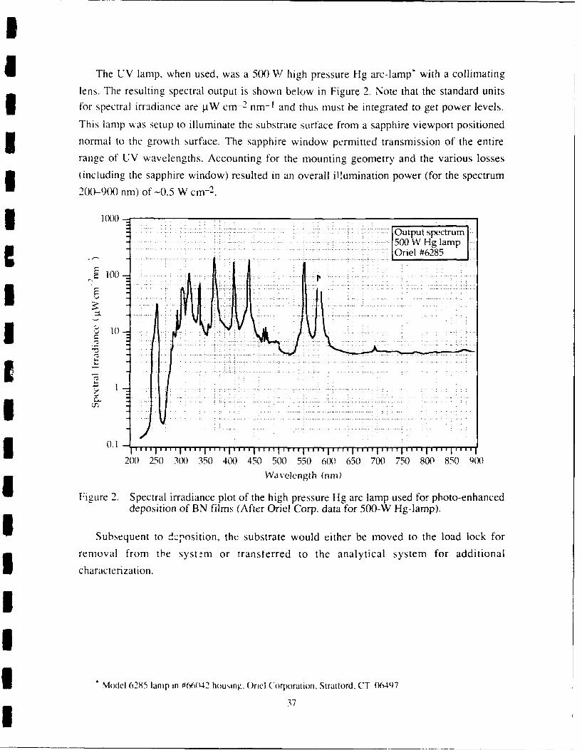
The UV lamp, when used, was a 500 V high pressure Hg arc-lamp* with a collimating
lens. The resulting spectral output is shown below in Figure 2. Note that the standard units
for spectral irradiance are iW cm- 2 nm- 1 and thus must be integrated to get power levels.
This lamp was setup to illuminate the substrate surface from a sapphire viewport positioned
normal to the growth surface. The sapphire window permitted transmission of the entire
range of UV wavelengths. Accounting for the mounting geometry and the various losses
(including the sapphire window) resulted in an overall illumination power (for the spectrum
200-900 nm) of -0.5 W cm-2 .
1 (X)O .
:Output spectrum....... 500 W Hg lamp. .. . . . . . ........ ...... . ..O riel #6285
100=rl."oo:-i : ..... .: - : . " : : . - - 7 ' : ....... .. ..... .....
a10
- i I i I~ iiil~ iiilIIIII~i~ i i i ii ..... ... ..... Ii l i I i
_ •I .:I I... .. ....... . .. .. .... .
0 .1 ,, , , ) ,,4I , , I , , ,, , , , i, , i , ,I , , , ,, , , I ,, I , ,200 250 3WX 350 4WX 450 500 550 6WX 650 700 750 800 850 9WX
Wavelength (irim)
Figure 2. Spectral irradiance plot of the high pressure Hg arc lamp used for photo-enhanceddeposition of BN films (After Oriel Corp. data for 500-W Hg-lamp).
Subsequent to dz:position, the substrate would either be moved to the load lock forremoval from the systm or transterred to the analytical system for additional
characterization.
*Modl 6285 lamnp in #(-)0")2 housing, Oriel (Corporation, Stratford, CT 06-497
37

I
C. Results
1. Boron Nitride
Boron Nitride on Copper. Figure 3 show s an XPS plot (Riber Mac2 analyzer) of BN
deposited on a Cu(1 10) substrate. Note lack of contamination from carbon and oxygen as a
result of the UHV deposition. Peak heights make it appear that the surface is primarily Cu.This is not strictly true, since the sensitivity factor for Cu-2p3/2 is -50x greater than that of
B-is and -lOx greater than N-Is. However, significant island formation of BN is strongly
suggested.
X-ray spectra (Rigaku Geigerflex) of films grown at two different temperatures are
shown in Figure 4. Note that the BN deposit seems oriented to the substrate given that only
one reflection is present, but highly defective. This is from the fact that an ordinariiy
forbidden reflection seems to be present. Deposition does not appear to be affected by theinfluence of the photon irradiation.
Deposition of BN on Cu (111) was also undertaken to determine effects of substrate
orientation. X-ray diffraction showed that the films showed no cubic and were h-BN or t-BN
(a planar disordered h-BN variant).
Cu2FW2 XPS-Mg anode 1Resolution: 1 eVICu (110) substrate
.6_Culr'Jv Cu
BSCu Culp
1000 900 8W 700 600 500 400 300 200 100 0
Binding Energy (eV)
Figure 3 XPS spectrum of BN deposit on Cu(l 10) substrate. Cu-2p3/2 sensitivity is -50xgreater than that of B- Is and -lOx greater than N-ls.
38
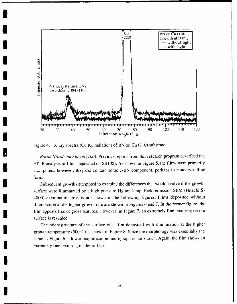
'Cu' BN on Cu 0110)(220) Growth at 500'C
....... without light[ with light
Nanocrvstalline BN?forbidden c-BN (110)
20 30 40 50 60 70 80 90 100 110 120Diffraction Angle (2 0)
Figure 4. X-ray spectra (Cu Ka radiation) of BN on Cu (110) substrate.
Boron Nitride on Silicon (100). Previous reports from this research program described the
FT-IR analysis of films deposited on Si(100). As shown in Figure 5, the films were primarily
a .i 1,.phous; however, they did contain some c-BN component, perhaps in nanocrystalline
form.
Subsequent growths attempted to examine the differences that would evolve if the growth
surface were illuminated by a high pressure Hg arc lamp. Field emission SEM (Hitachi S-
4000) examination results are shown in the following figures. Films deposited without
illumination at the higher growth rate are shown in Figures 6 and 7. In the former figure, the
film appears free of gross features. However, in Figure 7, an extremely fine texturing on the
surface is revealed.
The microstructure of the surface of a film deposited with illumination at the higher
growth temperature (500'C) is shown in Figure 8. Since the morphology was essentially the
same as Figure 6, a lower magnification micrograph is not shown. Again, the film shows an
extremely fine texturing on the surface.
iI
39i

R.N on Si (100)Transinision ET-IRIRc.-oluton: 4 cm CO,Nicole( 5lop
a-BN c-BN a-BN
V Op
4500 4000 3500 3000 2500 2000) 1500 1000 500Wavenumber (cm ')
Figure 5. Transmission FT-IR spectra of BN deposited on Si (100) substrate. Inverted C02absorption peak is present because concentration was lower when analyzing
sample than for instrument baseline spectrum.
II
* W,
FIg-ure 6. Scc:ondarv electron microviraph Of SUrface of BN film deposited on Si (I Wv)I' without aditional Hilumination gvrowth at 5M( C).
1 40

A Mt
25 ' t
a~ 4_
0
IFig'ure 7. Sconidary elctron mcrogrnaph ofsurface of BN film deposited on Si (1))twttadditiona l illuination ol I VLIC (groAth at 5 0'C).

Growth at a lower temperature (4000 C) resulted in the surface morphologies shown inFigures 9 and 10. They reveal a small but discernable change from those shown in Figures
6-8. The higher magnification micrograph of Figure 10 shows small grains across the surface.F1'igure 11 shows the surface microstructure for films grown at 400CC in tandem %kith the
illumination from the arc lamp. The microstructure at low magnification was similar to thatof Figure 9 and so is not shown. The microstructure is more like that of the finms deposited at500,C, than that of the 400'C film without illumination. However, the change in appearance
is slight.3 Showkn in Figure 12 are the diffraction patterns from depositions at 500'C. Note that thesaMIple with illumination fractured from handling which resulted in a high background at lowangles due to the scattering from mounting clay. The interesting feature is that the c-BN
(400) peak is not present except when the growth surface is photon irradiated.
I
2.5 g~m
I -gure 9. Se:onidary electron micrograph Of surface of BN film deposited on Si (100)without additional illumination (growAth at 4000C).
I
34
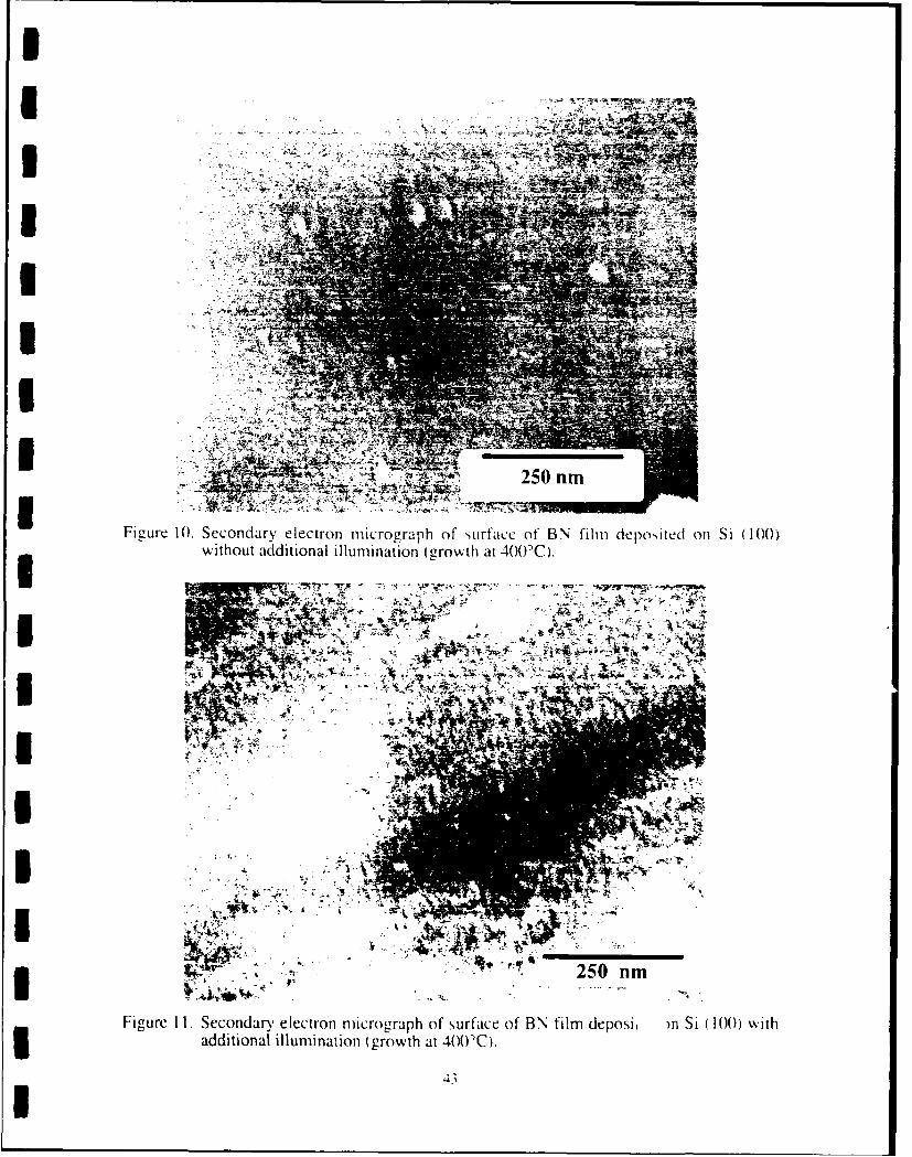
L
Z" A
IWI
.f
Figure 10. Secondary electron micrograph Of Surface of N' film ieposite n S (100) itwihuadditional illumination growth at 40C
I 1-

II
High Bkgd Si0\nanoxtal BN? BN on Si (100)from HighnBkg (200 nanlBN Growth at 500"Cfrom mounting c-BN (220) _- with light
- without lightSi
(200)
c--
I5
h-N nanocrystalline T3N? (400)
(00 02)
20 3(0 40 50 60 70 80 90 100 110 120Diffraction Angle (2 E)
Figure 12. X-ray diffraction patterns (Cu Ka radiation) of BN deposited on Si (100) at 500°Cwith and without illumination from the Hg arc lamp.
Samples were next compared at a lower growth temperature to determine its impact on
the phase formation. Figure 13 shows patterns from depositions at 400°C. The h-BN phase is
apparently much more well crystallized at this lower temperature, based on the narrow
linewidth of the h-BN (W002) peak. In both cases, the c-BN (400) peaks are present, but there
is a dramatic decrease in the intensity of the h-BN (0002) peak for the illuminated case.
indicating a strong inhibition of the formation of this phase.
The FT-IR spectra from the samples grown at 500'C are shown in Figure 14 and show
that there is little else evident than the two phases of BN. Please note that peaks for
amorphous BN coincide ,ith those of h-BN and thus are not differentiated in these spectra
(see discussion).
The FT-IR spectra for the samples grown at 400'C are shown in Figure 15 and show a
much more complex structure. Note the many water and carbon dioxide peaks are from a
purging problem in1 the optical analysis bench and can be ignored. Interestingly, the complex
peak structures for the unirradiated case disappeared for the case when the photon irradiation
was used. This is not contamination as has been shown in man) previous reports from XPS
spectra.
44

Si BN on Si (100)h-BN (40) Grwhat 400'C(0002) - with light
....without light
I -BI. '-forbidden c-BN (110)I0
20 30 40 50 60 70 80 90 100 110 1203 Diffraction Angle (2 0)
Figure 13. X-ray diffraction patterns (Cu K~x radiation) of BN deposited on Si (100) at 400'Cg with and without illumination from the Hg arc lamp.
Ih-BNcBN h-B
J K
I BN oin Si (100)Growth: 500'-C..............without light
-with light
45MX 40M0 35WX 30M0 25X 2M)0 15C00 10(XM 5W0
Wavenumber (cm I
Figure 14. FT-IR spectra (Nicolet 5 1lOP) of BN on Si (100) deposited at 500'C.
1 45

I
3 Water peaks CO 2 peaks Water peaks
3 c-BN h-BN
I A
IBN on Si(100)
Growth: 400'C-with light........ without light
4500 4000 3500 3000 2500 2000 1500 1000 500Wavenumber (cm 1)
Figure 15. FT-IR spectra (Nicolet 510P) of BN on Si (100) deposited at 400'C. Spectracorrected for background shift and slightly smoothed.
2. Gallium NitrideThe XPS spectra in Figure 16 show no noticeable differences between films deposited
with and without the lamp illumination.
Field emission SEM (Hitachi S-4000) examination results are shown in the following
figures. Films deposited without illumination at the higher growth rate are shown in
Figures 17 and 18. The film appears free of gross features in Figure 17, but Figure 18 shows
an angular texture indicative of a polycrystalline film.
Films deposited with illumination at the higher growth rate are shown in Figures 19 and
20. Again, the film appears free of gross features in Figure 19, but Figure 20 shows a
different angular texture indicative of a polycrystalline film, as before, yet certainly different
in some respects.
Films deposited without illumination at the lower growth rate are shown in Figures 21
and 22. The film appears much flatter than at the higher growth rate and with a significantly
different texture. Large crevice-like features are also clear in Figure 21. Figure 22 shows the
texture tends to be in two directions, but with smaller areas with a different texture.
46

GaLMM GaIM.\al MM
* N,
3~ aZI
t a -VIL
g Ga G
1000 1400 800) 700 600) 500 400 300 200 100 03 Binding Energy (eV)
Figure 16. XPS spectra of GaN on 1-SiC(100) deposited with and without illumination from3 500-W Mg-arc lamp.
l
T4.4
tIi3w
~S
Eioure 17. Secondary elec2tron micrograph Of SUrface of GaN film deposited on P-SiC (100)W ithout addiitional -Illumination tGa cell (@ 990'C).
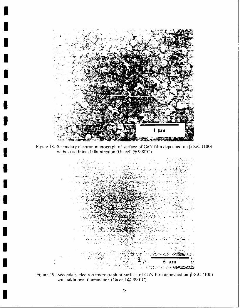
-402I .A 4W_
IR
Figure 18. Secondary electron micrograph of surface of GaN film deposited on P-SiC (1(10)3without additional illumination (Ga cell @ 9900 C).
3 ~> * S - ~.~ts
3 AWI t
Slit -iv
* ~;MN
Figure 19. Secondary electron mnicrogzra ph of surfaice of GaN film deposited on a-SiC (100)U with additional illumination (Ga cell Cqgp 9903C).
* 48

1 42
I
II
5 gm
FI(_,ure ~ ~ 21 eodr-lcrnmcorp fSrfc lG Nfl eoie nP C 10
4ih~ ddtoa ilu iatio (G elCa 7c
~ .4'I49

IA
I ... -.- 4
A'"M
Figur 22 .Seodr lcrnmcorp fsraeo a imdpstdo -I 10without additional ~iluiainG clCa97C)
Fiueq.uendy eleron micogapfsure offl depositedon thicnes (100)akcatee
along withoutpadiionvale illumination Ga c ellc decie latr.Itapeasha
th adition deoted wiothn illumiation dea thee growth rate byarsowninFues 23 and/
24 ~T lpear mu.Thchnesoer in FguNlyrs ep3 tn indprevise itonlyae
~~mesrdhbcsatrdelectron imaging ind acil msinSM(EL60 .Teeressus e own inabl.I
('OndItI I 01\TeCh 1 ie BEI-SEM XTEM Growth rate
Gjakit99( ' C \w/o light 550 nmi 550 nmi 183 nm/h(ia(&9900-C \,%/ light 500 nni* 450-500 nm* 161 nmn/hI (a0)975_( \A,/o lighJt 400 nim 420 nmi 137 nmn/hGac(L975 C wx/ l ighit 360) nmi 350 rim H1 8 nm/h
U Increascd 'surlacc noughnes\s nadc this niwsucenieni difficult.
3 50
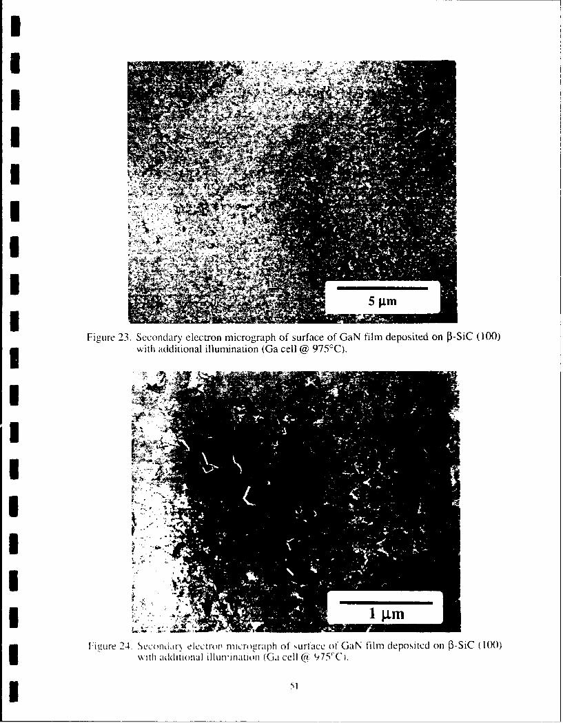
I&
I ~
UA ith d iinliluvnt? G el (.I7' )
3 fr.~ # ' 4 ' __ ____ __51
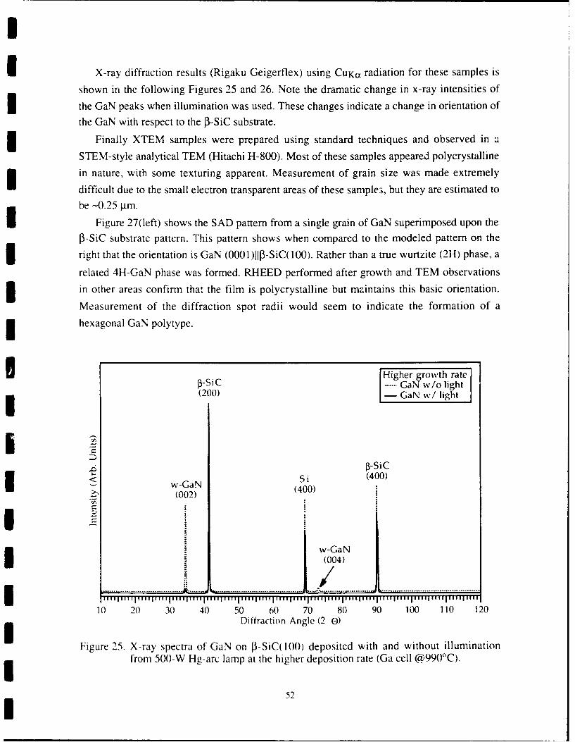
X-ray diffraction results (Rigaku Geigerflex) using CuKO' radiation for these samples is
shown in the following Figures 25 and 26. Note the dramatic change in x-ray intensities of
the GaN peaks when illumination was used. These changes indicate a change in orientation of
the GaN with respect to the [3-SiC substrate.
Finally XTEM samples were prepared using standard techniques and observed in a
STEM-style analytical TEM (Hitachi H-800). Most of these samples appeared polycrystalline
in nature, with some texturing apparent. Measurement of grain size was made extremely
difficult due to the small electron transparent areas of these samples, but they are estimated to
be -0.25 jtm.Figure 27(left) shows the SAD pattern from a single grain of GaN superimposed upon the
P-SiC substrate pattern. This pattern shows when compared to the modeled pattern on the
right that the orientation is GaN (0001)I[-SiC(100). Rather than a true wurtzite (2H) phase, a
related 4H-GaN phase was formed. RHEED performed after growth and TEM observations
in other areas confirm that the film is polycrystalline but maintains this basic orientation.
Measurement of the diffraction spot radii would seem to indicate the formation of a
hexagonal GaN polytype.
Higher growth ratef-SiC ....... GaN w/o light(200) GaN w/ light
i P-sic<Si (400)
w-GaN Si(40(002) (400)
i I w-GaN
.............................. ...... . ..... ,.......,... ........ .. , . ..., .. ................. ..................................................
10 20 30 40 50 60 70 80 90 100 110 120Diffraction Angle (2 0)
Figure 25. X-ray spectra of GaN on P-SIC(100) deposited with and without illuminationfrom 500-W Hg-arc lamp at the higher deposition rate (Ga cell @990'C).
52
frSi Loe Growth Rate(200) without lght
wihlight
ISi 3-SiC(400) (400)
w,-GaN(002)
c-GaN
c-GaN(400)
[(200) jw-GaN(00410 20) 30 40 50 60 70 80 90 100 110 120
Diffraction Angie (2 e)Figure 26. X-ray spectra of GaN on D-SiC(1OQ) deposited with and without illumination
from 500-W Hg-arc lamp at the lower deposition rate (Ga cell @975'C).
(01?2) *02
IFig'ure 27. SAL) pattern ifrom) one polycrystalline grain of GaN on P-SiC (100) at lowergrowAth rate (Ga @a975CC) without illumination during growth. Left: Real pattern.3 Right: Model showin- orientabion (z=[0 11]).
figr 28Xdeft 1 shiows the SAD pattern from a polycrystalline region of GaNStIperiiposed upon the O-SIC substrate pattern. Very dim spots near the center confirm the
I 53

continued presence of 4H-GaN from the (0002) reflection. The three rings correspond to the
(1010), (1011), and (2020) rings. This much more random pattern is reflected in the
roughness of the surface observed in SEM and the much reduced diffraction intensities.
RHEED performed after growth also confirmed the polycrystalline nature of the film.
I :(200): (01iToy
- .000 ) :.:. '* . • *-:(0227)
* N.,*o e
Figure 28. SAD pattern from polycrystalline patterns of c-GaN and 4H-GaN on P3-SiC (100)at lower growth rate (Ga @975CC) with illumination during growth. Left: Realpattern. Right: Model showing orientation (z=[01 1]).
TEM confirmed the x-ray diffraction analysis as well as the SEM observations indicating
that in some regions the film was 4H-GaN and in other regions the film was cubic GaN. In
regions where the film was cubic GaN, the previously observed orientation was seen, namely
(200)11(200) and (025)11(022). Figure 29(left) shows the SAD pattern from a 4H-GaN region
superimposed upon the P-SiC substrate pattern. This pattern, when compared to the modeled
pattern on the right, shows that there are two orientations of the 4H-GaN to the P3-SiC
substrate. This pattern is very similar in general appearance to that for the cubic GaN case
and explains why it would be difficult to differentiate the patterns using RHEED. The
relationships observed are as follows: (fl 1)11(0004) and (600)11(0338) as well as (11 i)l(0004)
and 044)11(0318). The SAD pattcrn also shows evidence of streaking in both of the (0001)
directions observed.
TEM confirmed the x-ray diffraction analysis as well as the SEM observations indicating
that the filn was single crystal 4H-GaN. The orientation relationship observed was
(200)11(0002) and (0L)11(20-50). Figure 30(left) shows the SAD pattern from the 4H-GaN
region superimposed upon the P-SiC substrate pattern. Again streaking in the (0001)
54

III
Idirection is observed indicating defects present in the GaN film. This is confirmed incomparing the x-ray diffraction and SEM results.
I
Figure 29. SAD pattern from twinned 4H-GaN on D-SiC (100) at higher growth rate (Ga@990'C) with illumination during growth. Left: Real pattern. Right: Modelshowing orientation (z=[01 1]).
I
£(flo)I0 0 A002)0
I ". • *
IFigure 30. SAD pattern from single crystal 4H-GaN on [-SiC (100) at higher growth rate
(Ga (990'c) with illumination during growth. Left: Real pattern. Right: Modelshowing orientation (z=[0 111).
II 55

I!
The texturing observed in the SEM is also confirmed in the bright field image shown inFigure 31. The columnar structure is evident as well as strain contrast at the GaN/P3-SiC
interface.
liaII "-
It
• GaN layer
-I
I-SiC substrate 0.1 m
Figure 31. Bright field image of single crystal 4H-GaN on 1-SiC (100) (z=[01 1]).
D. Discussion1. Boron Nitride
Boron Nitride on Copper. Copper was chosen primarily because of its near perfect latticematch (Aa =0.022%). The thermal expansion difference is slight (=10 ppm/0 C) and actually
improves the lattice match at growth temperatures. Copper does form a complex cubic nitride
(Cu3N). Its lattice parameter (3.815 A)[601 is only =5% larger than c-BN. The surface energydifference is a problem, as copper has a much lower surface etiergy than c-BN (1430 vs.
4770 erg/cm 2 ).[5, 611 This problem plagues c-BN heteroepitaxial deposition on everysubstrate except c-BN on diamond.
56

I
An additional potential advantage in the use of copper substrates relates to the use of
nitrogen as a surfactant in the growth of c-BN films. Surfactants have been used successfully
in the system Si/Ge/Si to suppress island formation.[62] Dosing Cu with atomic N does form
the cubic Cu3 N phase[63], noted above. It is not a strongly bonded compound and
I decomposes at temperatures in the range of 300-500'C.[63, 64] A cubic Cu4N phase has
also been reported. It is more difficult to form than Cu3N. The lattice parameter of the Cu4N
phase is 3.193 A. It decomposes above =55 0 'C.[65]
X-ray diffraction indicated the presence of some phase with cubic character, perhaps a
highly defective c-BN. Since the observed (110) reflection is forbidden, it would need to be a
highly defective structure. There were no apparent differences in the diffraction patterns as a
result of the addition of photon illumination during growth. As discussed in the Introduction,
photon effects can be affected strongly by the influence of the substrate, thus this result is not
necessarily surprising.3 Deposition was also performed on Cu(1 11) to determine if the BN deposition was at all
affected by interaction with the substrate. Subsequent x-ray diffraction showed the film to be
3 strongly h-BN or t-BN.
Boron Nitride on Silicon (100). Films deposited and discussed in previous reports were
analyzed via FT-IR as was shown in Figure 5. These analyses indicate some cubic-character
to these predominantly amorphous films. .s noted above, the peaks for amorphous BN
coincide with those of h-BN and thus were not differentiated in this spectrum, but are
assigned to a-BN as a result of earlier x-ray and TEM analysis.The Introduction section showed how photon irradiation could change many kparameters3 in thin film growth, and so a high pressure Hg lamp was selected to illuminate samples
during deposition. Figures 6-8 show the BN surfaces after deposition at 500'C coupled with3 illumination from the Hg lamp. The surface morphology appeared completely unchanged by
the effects of the illumination. This extremely fine texture is most likely due to bombardment
effects from the ECR source, as similar textures have been observed occasionally in GaNdeposition.
The surface morphology of samples deposited at 400'C was changed somewhat, as3 documented in Figures 9-11. Small "grains" of material appeared in the surface of the
otherwise identically textured surfaces. In this case, the illumination did change the
morphology slightly making it more uniform. Comparison of these SEM figures with the x-
ray diffraction patterns suggested that the "grains" observed in Figure 10 are h-BN, which
were desorbed or prevented from forming as a consequence of the illumination (see Figure
11).
Figure 12 shows that the addition of illumination helped to initiate the formation of the
c BN phase which otherwise did not occur, or did not occur in such an oriented fashion.
I 57
I
Details of this possible orientation effect must await TEM analysis. Figure 13 shows that the
illumination dramatically decreased the h-BN (0002) peak intensity, which correlates well
with the SEM observations already discussed. It was not expected that since a sharp c-BN
(400) peak exists that a c-BN (200) would not exist. The scattering factors are such that the
(200) peak should be as strong or stronger than the (400) peak. However, this strange
outcome has been reported previously in the literature.[63-66] No reasonable explanation
has been put forward to describe this unusual phenomenon.
The FT-IR analysis presented in Figure 14 shows the nature of the films deposited at
500'C. Small changes in the appearance of the peak heights occurred as a result of the UV
illumination. This would seem to indicate that the presence of the c-BN peak reflects bonding
of a cubic character rather than cubic structure, as is the case for the two h-BN peaks. Thus,
while the crystallinity changes as indicated by x-ray diffraction, the bonding character in the
larger volume of amorphous film is not dramatically affected. Deposition at 400'C involves a
more dramatic change, as shown in Figure 15. The h-BN and c-BN peaks are both definitely
less intense. This would indicate a dramatic reduction in the h-BN component of the film,
with the peaks remaining from the amorphous component. The reduction in the c-BN peak is
not understood at this time, since the x-ray diffraction peaks for the c-BN phase are virtually
the same. It may be due to a reduction in the sp3 bonding in the amorphous phase. The many
peaks in the low wave number range of the unirradiated case are also not understood. Given
the purity of the films, these are most likely due to defect structures which are effectively
removed by the addition of the illumination. Again, much of this explanation will need to
await TEM analysis.
2. Gallium Nitride
The XPS spectra in Figure 16 show no noticeable differences between films deposited
with and without the lamp illumination. Higher resolution scans around the Ols and Clspeaks (not shown) revealed undetectable levels of contamination in both cases. Thus, further
XPS analysis was not performed.
The surface morphology of the films might be expected to be quite different for films
deposited with illumination from the lamp, if surface mobilities are changed as expected.
Figures 17-21 clearly demonstrate this fact. The films are basically free from gross features
which cannot be related to defects in the substrate surface, but the fine structure of the
morphology is different in each case. Figures 17 and 18 show a film grown at a higher
growth rate without illumination. This film appears to have a granular texture to it, a common
feature of polycrystalline films. Figures 19 and 20 show a different granular texture, due to
the effects of the photon irradiation. The features appear much rougher than the previous
example, and have an, on average, different shape than before. RHEED after growth
58

I
indicated that these films were in fact polycrystalline, and had different orientations, which
explains the appearance of the growth surface.
X-ray diffraction results in Figure 25 show that this change in orientation, as the
unirradiated case, produced strong GaN diffraction peaks and the irradiated case did not. Thiswould mean that the unirradiated case had a very strong (200)11(0002) texture, and the
irradiated case did not, which would have strongly reduced the peak intensities. Thus the x-
ray results correlate very well with the RHEED and SEM observations.
In an attempt to get single crystal material, the growth rate was lowered. This comparison
is shown in Figures 21-24. Figures 21 and 22 show growth without illumination and again
the surface morphology is different, with a much more uniform appearance than observed
previously. However, areas are observed with varying morphology, indicating
nonuniformities. RHEED after growth, was difficult to interpret due to streaking, however it
appeared to be single crystal cubic GaN or something approaching single crystal in nature.
Figures 22 and 23 show a dramatically flattened surface when using the photon irradiation.
This surface shows a very good flatness with only a few hillock-like features. There seems to
be a very fine structure that can be seen in the surface of the film. RHEED after growth
would indicate a single crystal film with good flatness.
X-ray diffraction results in Figure 26 show this change in orientation, as the unirradiated
case had strong cubic GaN peaks with weaker wurtzitic GaN peaks. (Note the Si (400)
intensity is reduced in the unirradiated case, indicating poorer alignment of the substrate in
the diffractometer, a difficult problem in a system designed for handling powders.) The
irradiated case had only strong wurtzitic GaN peaks indicating a strong texture or a single5 crystal of GaN. Thus the x-ray results correlate very well with the RHEED and SEM
observations. This is especially true for the unirradiated case where two phases appear in the3 x-ray diffraction data and areas of differing morphology appear in the micrographs.
XTEM analysis of these samples is shown in Figures 27-31 and indicate the observation
of a new polytype of wurtzitic GaN, namely 4H-GaN. This polytype has lattice parameters of
a=0.318 nm and c=1.033 nm, or the same parameters as wurtzitic (2H) GaN, but with a c-axis 2x larger than normal. This is due to a modified stacking sequence. Normal wurtzite has
5 a stacking sequence of abab, while 4H material has a stacking sequence of abcb. Thus 4H-
GaN can be interpreted as either wurtzitic GaN with regular stacking faults or atom-layer3 twinned cubic GaN (the ultimate micro-twin). In cases where (200)11(0002), it will be
interpreted as stacking faults and where (111)11(0004) it will be interpreted as perfectly
regular twinning in cubic GaN.
Figure 27 shows the SAD pattern and diffraction model of the GaN deposited without5 illumination at the higher growth rate. Though the pattern was from a single grain, the film
1 59

I
was definitely polycrystalline, indicating a strong (200)11(0002) texture to the 4H-GaN
deposited. Under illumination, the film developed a different texture as shown in Figure 28,
showing a much reduced (200)11(0002) character. This is a rather suprising result with no
clear explanation at present.Figure 29 showed the results from the GaN deposited at a reduced growth rate without
illumination, which produced cubic GaN with localized twinned regions to give the
Sappearance of 4H-GaN. Growth with illumination produced single crystal, albeit defective,4H-GaN, as shown in Figure 30. The orientation relationship found was (200)11(0002) and
1 (022)11(2020). This relationship is somewhat unexpected as the film shown in Figure 27 had
assumed a similar orientation, but with addition of the photon irradiation, it changed to acompletely different one as illustrated in Figure 28. Furthermore, since the JP-SiC(100)
surface has four-fold symmetry and the 4H-GaN(0002) surface has six-fold symmetry the4H-GaN must follow a two-dimensional coincidence boundary rather than a more regular
alignment of lattice sites on the surface.
Finally, Figure 31 relates the structure seen in Figure 30 and the morphology observed inFigure 20. The columnar structure that is seen in Figure 31 appears similar to the surface
structure observed in Figure 20, so that the observed surface morphology extends well intothe GaN layer. The GaN/0-SiC interface appears sharp with strain contrast appearing due to
the misfit between the materials.
E. Conclusions1. Boron Nitride
Boron Nitride on Copper. Films of a highly defective and nanocrystalline c-BN nature
were deposited on Cu (110). Films deposited on Cu (111) were clearly different and of a
h-BN character, indicating that the substrate had a strong influence on the crystal structure of
the BN films.Boron Nitride on Silicon (100). Films deposited without photon irradiation and reported
previously were analyzed in this reporting period. These films contained material with cubic
character, as revealed by FT-IR studies. Ultra-violet irradiation was shown to have a definite
effect on the deposition of the BN films. At 500'C, it enhanced the crystallization of the
c-BN phase and did not encourage the formation of h-BN. At 400'C, photon irradiation
clearly inhibited the formation of the h-BN phase, which had previously formed more readily
at that temperature and did not inhibit the crystallization of the c-BN phase. Illumination of
the growth surface also appeared to reduce certain types of cubic-like character in the film,
but also removed other types of bonding defects present in the films.
60
1 2. Gallium Nitride
Films containing a new polytype of GaN, namely 4H-GaN, were grown. Photon
3 irradiation was clearly shown to change the growth rate, morphology, and crystalline phase
orientation to the P-SiC substrate. Changes in each of these properties were documented in
3 detail using RHEED, x-ray diffraction, field emission SEM (both secondary and back-
scattered), and electron diffraction.
U F. Future Research Plans/Goals1. Boron Nitride
Boron Nitride on Copper. Evaluation of these films will continue to determine if the
lattice match of Cu substrates can be exploited to produce c-BN films. Thin-film reflection
FT-IR will be used to determine the amount of amorphous component present. Should these
films become sufficiently large in extent, they will be floated from the substrate and analyzed
3 via TEM.
Boron has a low solubility in copper (=0.5 at.%). If boron were diffused into copper at a
high temperature and then cooled the boron would migrate to the surface. Since the boron
species would migrate to sites on the copper surface, they would already possess the same
symmetry as would be present in c-BN. Subsequent exposure to atomic nitrogen from the
plasma source and reaction with the diffusing boron would allow the c-BN phase to form
more readily and more uniformly across the surface of the copper substrate. This would not
Sonly improve the phase stability but help to resist the driving force for island formation which
is quite strong for c-BN on copper. Some boron diffusion and implantation have already been
3 conducted, the deposition of BN on these samples will be performed during the next
reporting period.
Boron Nitride on Silicon (100). The first priority will be TEM analysis of the deposited
films to determine (1) the extent of the c-BN deposition that has occurred, and (2) if any
other photon irradiation effects can be observed. Experiments will be conducted using3 selective bandpass filters on the light source to determine if a strong or weak wavelength
dependence is present and where in the spectrum of the light source it occurs. Finally,£ experiments will be initiated to determine if these photon-induced reactions can be made to
occur after deposition and to see if the effects are in the bulk or strictly growth surface
3 related.
2. Gallium Nitride
* An extension of the research described above to still lower growth rates will be
undertaken in an attempt to determine what phase effects will exist in a pure cubic-phase
GaN. Should a transition from cubic to wurtzitic occur as a result of UV illumination as the
1* 61

I
present evidence indicates, this would be solid, additional proof of the photophase effect inwide bandgap semiconductors. Analysis of the defects in those films will be conducted to
determine if the defect density is reduced by photon irradiation. The electrical properties will
also be evaluated on irradiated and unirradiated samples.
G. References1. R. H. Wentorf Jr., J. Chem. Phys. 36, 1990 (1962).
2. R. M. Chrenko, Solid State Commun. 14, 511 (1974).3. C. Deshpandey and R. F. Bunshah, Thin Solid Films 163, 131 (1988).4. N. Miyata, K. Moriki, and 0. Mishima, Phys. Rev. B 40(17), 12028 (1989).5. R. C. DeVries, Cubic Boron Nitride: Handbook of Properties, Technical Information
Series, General Electric Company, Corporate Research and Development, 72CRD178,1972.
6. K. H. Seidel, K. Reichelt, W. Schaal, and H. Dimigen, Thin Solid Films 151(2), 243(1987).
7. M. Mieno and T. Yoshida, Jpn. J. Appl. Phys. 29(7), 1175 (1990).8. M. Satou and F. Fujimoto, Jpn. J. Appl. Phys. 22(3), L171 (1983).9. Y. Andoh, et al., Nucl. Instrum. Meth. Phys. Res. B19/20, 787 (1987).
10. J. Kouvetakis, V. V. Patel, C. W. Miller, and D. B. Beach, J. Vac. Sci. Technol. A 8(6),3929 (1990).
11. H. Saitoh, T. Hirose, H. Matsui, Y. Hirotsu, and Y. Ichinose, Surf. Coat. Technol. 39-40(1-3), 265 (1989).
12. M. Okamoto, H. Yokoyama, and Y. Osaka, Jpn. J. Appl. Phys. 29(5), 930 (1990).13. A. Chayahara, H. Yokoyama, T. Imura, and Y. Osaka, Appl. Surf. Sci. 33/34, 561
(1988).14. 0. Matsumoto, M. Sasaki, H. Suzuki, H. Seshimo, and H. Uyama, in Tenth InternationalConference on Chemical Vapor Deposition. G. W. Cullen, Eds. (The ElectrochemicalSociety, Honolulu, Hawaii, 1987), pp. 552.
15. T. Ikeda, Y. Kawate, and Y. Hirai, Kobelco Technol. Rev. 6, 1 (1989).16, M. Murakawa and S. Watanabe, Surf. Coatings Technol. 43/44(1-3), 128 (1990).17. T. Nagatomo, Y. Hatooka, and 0. Omoto, Trans. IECE Jpn. E 69(4), 482 (1986).18. T. Ikeda, Y. Kawate, and Y. Hirai, J. Vac. Sci. Technol. A 8(4), 3168 (1990).19. A. R. West, Solid State Chemistry and its Applications (John Wiley & Sons, Chichester,
1984).20. F. N. H. Robinson, Phys. Lett. A 26(9), 435 (1968).21. Z. Sitar, etal., Mat. Sci. Lett. preprint, preprint (1991).22. P. D. Fleischauer, in Concepts of Inorganic Photochemistry A. W. Adamson, and P. D.
Fleischauer, Eds. (Wiley-Interscience, New York, 1975), pp. 439.23. R. Solanki, C. A. Moore, and G. J. Collins, Sol. State Technol. 28(6), 220 (1985).24. B. A. Joyce, J. Phys. Chem. Solids 49(3), 237 (1988).25. T. Y. Sheng, Z. Q. Yu, and G. J. Collins, AppI. Phys. Lett. 52(7), 576 (1988).26. T. Yamazaki, S. Watanabe, and T. Ito, J. Electrochem. Soc. 137(1), 313 (1990).27. A. I. Kingon, 0. Auciello, M. S. Ameen, S. H. Rou, and A. R. Krauss, Appl. Phys. Lett.
55(3), 301 (1989).28. A. Lietoila, R. B. Gold, J. F. Gibbons, and L. A. Christe, in CWBeam Processing of
Silicon and Other Semiconductors J. F. Gibbons, Eds. (Academic Press, New York,1984), pp. 71.
29. J. A. Van Vechten, R. Tsu, F. W. Saris, ani D. Hoonhout, Phys. Lett. 74A(6), 417(1979).
30. J. A. Van Vechten, R. Tsu, and F. W. Saris, Phys. Lett. 74A(6), 422 (1979).31. Z. Yu and G. J. Collins, Phys. Scripta 41(1), 25 (1990).
62

I
3 32. M. Kitagawa, Y. Tomomura, K. Nakanishi, A. Suzuki, and S. Nakajima, J. Cryst.Growth 101, 52 (1990).
33. N. Matsumura, T. Fukada, and J. Saraie, J. Cryst. Growth 101(1-4), 61 (1990).34. K. L. Chopra, L. K. Malhotra, K. S. Harshavardhan, and S. Rajagopalan, Bull. Mater.
Sci. 6(6), 1013 (1984).35. R. N. Bicknell-Tassius, A. Waag, Y. S. Wu, T. A. Kuhn, and W. Ossau, J. Cryst. Growth
101(1-4), 33 (1990).36. W. A. Young, M. Y. Mirza, and W. W. Duley, Opt. Commun. 34(3), 353 (1980).37. W. I. Milne, F. J. Clough, S. C. Deane, S. D. Baker, and P. A. Robertson, Appl. Surf.
Sci. 43, 277 (1989).38. A. Gedanken, M. B. Robin, and N. K. Kuebler, J. Phys. Chem. 86, 4096 (1982).39. H. Okabe, Photochemistry of Small Molecules (Wiley-Interscience, New York, 1978).40. N. C. Giles, et al., J. Cryst. Growth 86(1-4), 348 (1988).41. N. C. Giles, K. A. Bowers, R. L. Harper Jr., S. Hwang, and J. F. Schetzina, J. Cryst.
Growth 101(1-4), 67 (1990).42. R. L. Harper, Jr., et al., J. Vac. Sci. Technol. B 7(2), 244 (1989).43. S. Fujita, A. Tanabe, T. Kinoshita, and S. Fujita, J. Cryst. Growth 101(1-4), 48 (1990).44. P. A. Kohl and F. W. Ostermayer Jr., in Annual Review of Materials Science R. A.
Huggins, J. A. Giordmaine, and J. B. Wachtman Jr., Eds. (Annual Reviews, Inc., PaloAlto, CA, USA, 1989), pp. 379.
45. H. Kokado, I. Simizu, and E. Inoue, J. Non-Cryst. Sol. 20(1), 131 (1976).46. A. Das and R. A. Jishi, Phil. Mag. Lett. 62(2), 107 (1990).47. G. Kluge, Phys. Stat. Sol. A 101(1), 105 (1987).48. T. Wolkenstein, Adv. Catal. Rel. Subj. 23, 157 (1973).49. S. R. Morrison, J. Catal. 20, 110 (1971).50. W. Ho, in Photochemistry in Thin Films. T. F. George, Eds. (SPI, Los Angeles, CA,
1989), pp. 157.51. J. P. Cowin, E. P. Marsh, W. Meier, T. L. Gilton, and M. R. Schneider, in
Photochemistry in Thin Films. T. F. George, Eds. (SPIE, Los Angeles, CA, 1989), pp.147.
52. F. G. Celii, H. H. Nelson, and P. E. Pehrsson, J. Mater. Res. 5(11), 2337 (1990).53. R. M. Feenstra and T. C. McGill, Physica B 117-118, (1983).54. M. V. Alfimov, I. L. Aptekar', A. E. Galashin, and E. A. Galashin, Sov. Phys. Dokl.
29(5), 404 (1984).55. A. Matsuda and M. Kikuchi, Sol. St. Commun. 12, 359 (1973).56. Z. Sitar, M. J. Paisley, D. K. Smith, and R. F. Davis, Rev. Sci. Instrum. 61(9), 2407
(1990).57. J. R. Vig, J. Vac. Sci. Technol. A 3(3), 1027 (1985).58. H. Lamb, private communication, 1990.59. I. Villegas, C. B. Ehlers, and J. L. Stickney, J. Electrochem. Soc. 137(10), 3143 (1990).60. V. R. Juza and H. Hahn, JCPDS Card #2-1156, Powder Diffraction File, JCPDS, 2-1156,
1938.61. C. R. Barrett, W. D. Nix, and A. S. Tetelman, The Principles of Engineering Materials
(Prentice-Hall, Inc., Englewood Cliffs, New Jersey, 1973).62. M. Copel, M. C. Reuter, E. Kaxiras, and R. M. Trump, Phys. Rev. Lett. 63(6), 632 (1989).63. D. Heskett, A. Baddorf, and E. W. Plumrnmer, Surf. Sci. 195(1-2), 94 (1988).64. M. Asano, K. Umeda, and A. Tasaki, Japanese Journal of Applied Physics 29(10),
1(85 (1990).65. J. Blucher, K. Bang, and B. C. Giessen, Mater. Sci. Eng. A 117, LI (1989).66. K. Inagawa, K Watanabe, K. Saitoh, Y. Yuchi, and A. Itoh, New Diamond, 60 (1988).67. K. Inagawa, K. Watanabe, H. Ohsone, K. Saitoh, and A. Itoh, J. Vac. Sci. Technol. A
5(4), 2696 (1987).68. G. L. Doll, in New Diamond Science and Technology. R. Messier, J. T. Glass, J. E.
Butler, and R. Roy, Eds. (Materials Research Society, Washington, DC, 1990), pp.xxi+1 128.
63

III
CUBIC BORON NITRIDE THIN FILMi SYNTHESIS BY MICROWAVE ECR PLASMA* CHEMICAL VAPOR DEPOSITION
* by
I M. J. Paisley, Z. Sitar, L. P. Bourget* and R. F. DavisDepartment of Materials Science and Engineering
Box 7919, North Carolina State UniversityRaleigh, North Carolina 27695-7907
*Applied Science and Technology (ASTeX), Incorporated35 Cabot Road
Woburn, MA 01801,II3 Submitted to
IKobe Engineering Reports
September 20, 1991
II
I

II
Abstract
Thin films of cubic boron nitride (c-BN) have many applications in areas such as
diamond substrates and optoelectronic devices in the vacuum ultraviolet. The objective of
I this study was :h, deposition of c-BN on Si (100) and (111) using microwave ECR plasma
chemical vapor deposition with borazine as the source material. Films were deposited and
analyzed employing the echniques of ellipsometry, x-ray photoelectron spectroscopy (XPS),
5 x-ray diffraction (XRD), transmission electron microscopy (TEM), and Fourier transform
infrared spectroscopy (FT-IR). Results indicated the deposited films were comprised of
I microcrystals of c-BN and oriented hexagonal BN as well as amorphous BN.
I. Introduction
The cubic polymorph of BN has received much interest recently as a possible substrate
for the deposition of diamond, due to the similar lattice parameters (Aa 0=1.34%) and its wider
bandgap which is in the range of 5.8-6.5 eV. 1- 3 The very wide bandgap of c-BN also gives
c-BN potential applications in its own right, as optical devices for the vacuum UV
(2 -200 nm) as well as more traditional applications such as a hard coating for machining
I ferrous metals. For a complete listing of materials-related properties of c-BN see Landot-
3 Brrnstein:Numerical Data and Functional Relationships in Science and Technology, Series
111, Vols. 17 and 23, or Ref. 4 (which also includes a side-by-side comparison of properties of
3 c-BN with diamond).
II. Experimental Procedure
n The depositions were carried out at the ASTeX, Inc. facilities in Woburn, MA a
microwave electron cyclotron resonance (ECR) plasma chemical vapor deposition (CVD)
systems adapted for handling BN precursor species. This involved installing a special mass
I flow controller calibrated for low vapor pressure gases and a bottle of borazine (B3N3H6)
liquid into the gas handling system. Borazine (analogous to the carbon compound benzene)
U has been used previously for deposition of BN films in CVD reactors, 5 - 7 but not with a
microwave ECR plasma source.
PAISLEY el al Kobe Engineering Reports Pg. 2I

The microwave ECR plasma CVD gas system consisted of a gas manifold and the
associated mass flow controllers which fed gases directly into the plasma or downstream near
the substrate. Depositions were performed with argon and nitrogen were injected directly
into the plasma, while the borazine was injected downstream. The 35 cm diameter chamber
was evacuated by an 880 1/sec turbomolecular pump (base pressure: mid 10- 7 Torr) backed
by a 50 cfm mechanical pump which was vented to an exhaust system. The substrate was rf
induction heated and its temperature calibrated with a thermocouple placed on the substrate's
surface. The substrate support was isolated, making it possible to add rf biasing to the
I substrate to independently control ion energy and ion flux to the substrate. A schematic
diagram of the ASTeX system is shown in Figure 1.
P!IIIII
PAISLEY et at Kobe Engineering Reports Pg. 3

Symmetric Microwave ComponentsPlasma M o1500 W Coupler Generator
ECR Source IGas Injection
3-Window Magnet
ECR Source-*-]:IIRemoteRem o
Exit MagnetIniection"
I
880 L/sec LoadlockTurbo Gate Valve
I, __,-Induction Heater
50 cfm with rf-bias capabilitv
pump
FIG. 1. Schematic diagram of microwave ECR plasma CVD system used at ASTeX, Inc.to deposit BN films.
PAISLEY et al Kobe Engineering Reports Pg. 4

II
Substrates of Si (111) or Si (100) were placed into a load lock and evacuated before
3 loading into the main deposition chamber. The samples were subsequently heated under
vacuum until the deposition temperature was reached. Finally, nitrogen and argon gas flow
I was begun, the plasma was ignited, and borazine flow was started which initiated deposition.
3 In situations where substrate bias was used, the plasma was initiated and the bias conditions
were established prior to deposition. The range of conditions used for deposition is shown in
3 Table 1.
Table 1. Deposition Conditions used in ECR CVD of BN.
Borazine flow 0.6 - 4.0 sccmNitrogen flow 0.0 - 20.0 sccmArgon flow 0.0 - 50.0 sccmChamber pressure 0.9 - 5.0 mTorrMicrowave power 500- 1000 WSubstrate temperature 590 - 6200CSubstrate rf-induced voltage 0to-65 VDCGrowth time (BN) 3 - 30 min.Deposited film thickness 50 - 2000 nm
I While applied rf power is often reported in the literature, this value is not nearly as
descriptive as the induced voltage that is reported in Table A. 1. When rf power is applied to
the substrate, a DC bias is induced on the substrate surface. This bias results in ions being
3 accelerated to the substrate surface. The rf bias was measured simply by attaching a
voltmeter between ground and the substrate holder with the addition of a low-pass filter to
I protect the voltmeter from rf voltages.
3After deposition, the samples were cooled and measured by a rotating polarizer type
ellipsometer to obtain index of refraction data. Finally, the samples were sent to NCSU for
5 further analysis.
III. Results and Discussion
I The resulting refractive index varied among the films over the range of 1.65-2.28, where
c-BN is n=2.12, and h-BN is n=2.02 {II c-axis) and n=2.22 (I c-axis)). 8 This would seem to
indicate a mixture of phases was present, with porosity or hydrogen incorporation accounting
IiI PAISLEY et al Kobe Engineering Reports Pg. 5

II
for the lower values measured. An x-ray spectrum of a film with n=2.01 is shown below in
3 Figure 2.
Si Si Si BNonSi(l1)(111) (222) (333) 1000 W gWave
5 sccm borazine20 sccrn nitrogen10 sccrn argon
Si X-ray: Cu K,,-~(111)
SCu K
21C- BN
20 30 40 50 60 70 80 90 100 110 1200Diffraction Angle (2 e)
3 FIG. 2. Typical x-ray spectrum from BN deposited on Si (111) substrate. Note BN regionwhich cannot be resolved into individual peaks present.
I The spectrum shows only a broad band of reflections in the region of 42-50' (20), which
3 covers a number of peaks from all phases of BN. The Si (111) Cu Kp peak is exactly where
predicted, but is unlikely since the detector has a graphite monochromator to greatly reduce
that peak. The h-BN (002) peak is either obscured in the lower edge of Si (111) peak, or has
shifted down slightly (i.e., the lattice expanded) and is where the Cu Kp peak should be. If
this were the case, its relative intensity would seem to indicate a significant portion of the
broad BN region is from phases other than h-BN. The fact that the region is continuous also
indicates at least some amorphous component. Analysis by XPS shown in Figure 3 shows
that the film is free from contamination other than carbon and oxygen. Much, if not all, of
this contamination is due to atmospheric exposure.
PAISLEY et al Kobe Engineering Reports Pg. 6
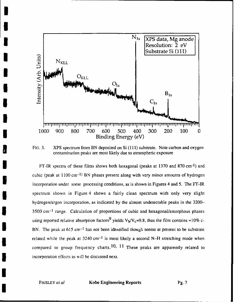
II
Njs XPS data, Mg anode
Resolution: 2 eVSubstrate Si (111)
~NKLL
O(KLLII
Ic s
1000 900 800 700 600 500 400 300 200 100 0Binding Energy (eV)
FIG. 3. XPS spectrum from BN deposited on Si (111) substrate. Note carbon and oxygencontamination peaks are most likely due to atmospheric exposure
FT-IR spectra of these films shows both hexagonal (peaks at 1370 and 870 cm- 1) and
cubic (peak at 1100 cm- 1) BN phases present along with very minor amounts of hydrogen
incorporation under some processing conditions, as is shown in Figures 4 and 5. The FT-IR
spectrum shown in Figure 4 shows a fairly clean spectrum with only very slight
hydrogen/argon incorporation, as indicated by the almost undetectable peaks in the 3200-
3500 cm- 1 range. Calculation of proportions of cubic and hexagonal/amorphous phases
using reported relative absorption factors9 yields Vh/Vc=9.8, thus the film contains =10% c-
BN. The peak at 615 cm- 1 has not been identified though seems at present to be substrate
related while the peak at 3240 cm-1 is most likely a second N-H stretching mode when
compared to group frequency charts. 10 , 11 These peaks are apparently related to
incorporation effects as will be discussed next.
PAISLEY et al Kobe Engineering Reports Pg. 7

I
BN on Si (111)3 IBorazine downstreamNicolet 51OP FT-IRScans avg'd: 32 N-H C2 h-BN h-BNResolution: 4 cm -1 stretch 2 -BN
0c-BN
|C
II- 615
450 4000 3500 3000 2500 2000 1500 1000 500Wavenumber (cm -t)
IFIG. 4. Fr-IR spectra of BN on Si(1 11) showing h-BN and c-BN peaks and very little
hydrogen/argon incorporation (0 V bias, 10 sccm Ar, WOO W).
PUIIIIUI
PAISLEY et al Kobe Engineering Reports Pg. 8I

II
N-Hstretch,j /f 'N =3240
I \ h-BN h-BNc-BN
..... - 2 V bias 50-.. .... 100 W..
I'
.... ""0 V"-. ' bias,," 50 sc,;,r,150
-6 V bias, 10 sccm Ar, 1000 W I
....20 V bias, 50 sccm Ar, 500 W '
I -20 V bias, 10 sccm Ar, 1000 W
4500 4000 3500 3000 2500 2)00 1500 1000 500Wavenumber (cm
FIG. 5. FT-IR spectra of BN on Si (111) under various processing conditions showingheavily distorted h-BN and c-BN (almost invisible) peaks, as well ashydrogen/argon incorporation.
I Figure 5 which shows spectra from several different deposition conditiuns. A comparison
of the spectra of Figures 4 and 5 reveal variations in intensity of the N-H stretch and
3240 cm- 1 peaks as well as both peaks for h-BN. The spectra in Figure 5 show strong peaks
3 of various intensities in the 3200-3500 cm -1 range and an apparent broadening of the B-N
stretching mode in the range from 1380-1550 cm- 1. The later relates either to a disordering
I effect from argon incorporation or perhaps the addition of a N-H bending mode which also
occurs in that region. 1 It seems that for Ar flow rates >10 sccm, or microwave power levels
I !PAISLEY et al Kobe Engineering Reports Pg. 9

II
: 000 W, or bias conditions < -20 VDC, cause hydrogen and perhaps argon to begin to be
incorporated into the growing film.
As a companion technique to the FT-IR analysis, samples were analyzed with Raman
I spectroscopy. Figure 6 shows a spectrum from the film indicating the highest fraction of c-
BN from FT-IR analysis. This spectrum reveals the presence of a mix of phases. Hexagonal
BN has one Raman active peak at 1368 cm -1 while c-BN has two peaks, namely the TO
(transverse optical) at 1055 cm- 1 and the LO (longitudinal optical) at 1308 cm-i. 1 2 These
values for BN were also confirmed by use of standards in the system used here. The h-BN
I phonon and the LO phonon of c-BN are clearly present, though apparently shifted slightly by
stress. In addition there is another weak peak at 1244 cm- 1 which has beer described as a
plasmon-phonon coupling mode by P. V. Huong.13 More importantly, this spectrum also
does not show the TO phonon mode at 1055 cm- 1, which may be due either to stress or other
effects not yet determined.USubstrate: Si(l11) h-BNAr Laser: 514.5 nm 1371I 200 mW spot intensity
c-BN LOI1295Plasmon-
Iphononcoupling
1244
950 1000 1050 1100 1150 1200 1250 1300 1350 1400 1450
Raman shift (cm -1)
FIG. 6. Raman spectrum of BN on Si (111) for sample showing highest c-BN fraction.
PAISLEY et al Kobe Engineering Reports Pg. 10

II
Samples from the conditions yielding the most c-BN were prepared for cross-section
I TEM using standard techniques. 14 A bright-field miciegraph of the cross-section region of
the film is shown in Figure 7. The measured film thickness was 0.7 pgm which corresponds to
a growth rate of 1.4 .m/h. The inset photograph shows the SAD pattern observed for this
film and indicates that the deposited layers are oriented h-BN with texture appearing to be
h-BN (002) II Si (11). Samples grown at high substrate bias condition ( 50 VDC)
I delaminated from the Si substrate, presumably due to induced stress from ion bombardment.
Pieces of the delaminated films were placed on nickel grids and examined in the TEM. SAD
patterns from a typical region of the BN layer showed very diffuse rings from a-BN. This
3 was especially true of the highest bias conditions (-65 VDC).
GleLine
| BN layerI•
Si substrate 0.5 gm
FIG. 7. XTEM photograph of BN on Si (111) with z=[110]. Inset shows SAD pattern ofSi with oriented polycrystalline h-BN.
While no c-BN was observed in the SAD patterns, this is not surprising given the low
concentration of c-BN and the polycrystalline/amorphous nature of much of the film. In
IiPAISLEY et al Kobe Engineering Reports Pg. 11

II
addition, many of the c-BN diffraction lines are very close to those of other phases of BN.
This makes unambiguous phase identification virtually impossible unless the diffraction
patterns are extremely sharp.
I IV. Conclusions
Boron nitride thin films depositeJ on Si via microwave ECR CVD from borazine and
nitrogen showed a mixed composition of amorphous, hexagonal and cubic phases of BN.
Evidence of hydrogen/argon incorporation was observed at high deposition power and bias
levels, as well as high argon flow rates. In addition, substrate biasing seemed to degrade the
I film quality, in contrast to the results reported by other workers. The authors think that zero
or low bias (0 < -20 VDC) levels would probably result in the best films using these source
gases.
V. Acknowledgements
The authors would like to acknowledge the support for this work from the Kobe Steel
3 Research Laboratories, USA as well as Applied Science and Technology (ASTeX), Inc.
Additional thanks go to L. Smith and R. C. Glass for the XPS and x-ray analyses.
I VI. References
1. R. M. Chrenko, Solid State Commun. 14, 511 (1974).
2. C. Deshpandey and R. F. Bunshah, Thin Solid Films 163, 131 (1988).
3. N. Miyata, K. Moriki, and 0. Mishima, Phys. Rev. B 40(17), 12028 (1989).
4. R. C. DeVries, Cubic Boron Nitride: Handbook of Properties, Technical InformationSeries, General Electric Company, Corporate Research and Development, 72CRD 178,1972.
3 5. R. R. Rye, J. Vac. Sci. Technol. A 9(3), 1099 (1991).
6. J. Kouvetakis, V. V. Patel, C. W. Miller, and D. B. Beach, J. Vac. Sci. Technol. A 8(6),3929 (1990).
7. S. Shanfield and R. Wolfson, J. Vac. Sci. Technol. A 1(2), 323 (1983).
8. K. H. Hellwege, ed., Landolt-Bdrnstein:Numerical Data and Functional Relationshipsin Science and Technology, Series III, Vol. 17 (Springer-Verlag, Berlin, Heidelberg,New York, Tokyo, 1987).
PPAISLEY et al Kobe Engineering Reports Pg. 12I

II
9. H. Yokoyama, M. Okamoto, and Y. Osaka, Jpn. J. Appl. Phys. 30(2), 344 (1991).
10. K. Nakamoto, Infrared and Raman Spectra of Inorganic and Coordination Compounds(John Wiley and Sons, New York, 1986).
11. R. C. Weast, ed., CRC Handbook of Physics and Chemistry (CRC Press, Inc., BocaRaton, FL, 1988).
12. D. R. Clarke and F. Adar, in Advances in Materials Characterization, edited by D. R.Rossington, R. A. Condrate, and R. L. Snyder (Alfred University, 1982), 199.
13. P. V. Huong, Diamond Relat. Mater. 1(1), 33 (1991).
14. J. C. Bravman and R. Sinclair, J. Electron Microsc. Techniq. 1, 53 (1984).
IIIII
IIIIII
PAISLEY et al Kobe Engineering Reports Pg. 13I