abstract generating linear models for the mos …
TRANSCRIPT
ABSTRACT
GENERATING LINEAR MODELS FOR THE MOS TRANSISTORS AND IMPLEMENTING
THEM IN OBTAINING BODE SURFACE PLOTS
Mounika Vanga, M.S.
Department of Electrical Engineering
Northern Illinois University, 2016
Dr. Reza Hashemian, Director
The CMOS transistors which have dimensions in nanoscale are modelled such that in a
circuit like an amplifier the original MOSFET can be replaced with the modelled circuit which
gives access to the internal nodes of the MOSFET. For generating the equivalent circuit, the
model components are generated from the model parameters. The models generated are tested by
comparing their response to that of the original MOSFET. These modelled devices are used in
generating the 3D Bode surface plots. A new method is developed which generates the 3D Bode
plot. This results in including the σ axis, along with the frequency and the magnitude axes into
the plots. For this purpose WinSpice is used as circuit simulator and MATLAB is used to
generate Bode surface by extracting results from WinSpice. A tool is developed which
integrates WinSpice and MATLAB so that in a comprehensive AC analysis Bode surfaces are
directly generated for any given analog circuit. This technique is shown to be ideal for the
identification, and hence the extraction, of poles and zeros of a transfer function. The
applications can be extended into analog filter design and stability analysis of control systems in
high-performance circuits.

NORTHERN ILLINOIS UNIVERSITY
DEKALB, ILLINOIS
MAY 2016 GENERATING LINEAR MODELS FOR THE MOS TRANSISTORS AND IMPLEMENTING
THEM IN OBTAINING BODE SURFACE PLOTS
BY
MOUNIKA VANGA
©2016 Mounika Vanga
A THESIS SUBMITTED TO THE GRADUATE SCHOOL
IN PARTIAL FULFILLMENT OF THE REQUIREMENTS
FOR THE DEGREE
MASTER OF SCIENCE
DEPARTMENT OF ELECTRICAL ENGINEERING Thesis Director:
Dr. Reza Hashemian

ACKNOWLEDGEMENTS
I would like to express my deepest gratitude to Dr. Reza Hashemian for his guidance and
continuous help in completing this thesis. His constant mentoring throughout my graduate study
has been a great help for me in becoming a better electrical engineer.
I would like to thank Dr. V.P.McGinn and Dr. Mansour Tahernezhadi for serving as
members of my thesis committee.
I would like to thank my family for their unconditional love, continuous support and
enduring patience. Finally, I would like to thank my friends who have directly and indirectly
helped me in completing my thesis.

I certify my thesis is devoid of any plagiarized material.

TABLE OF CONTENTS
LIST OF FIGURES ..................................................................................................................... viii
LIST OF TABLES .......................................................................................................................... x
CHAPTER 1 INTRODUCTION .................................................................................................... 1
CHAPTER 2 PROBLEM STATEMENT ....................................................................................... 3
CHAPTER 3 LITERATURE SURVEY ......................................................................................... 4
3.1 Classification of Roots and Respective Extraction Techniques .............................................4
3.1.1 Roots that Lie on Imaginary Axis ...................................................................................5
3.1.2 Passive RC Circuit with Roots on RLHP ........................................................................5
3.1.3 Active RC Circuit with Roots on RLHP .........................................................................8
3.1.4 RL Circuit with Roots on RLHP .....................................................................................8
3.1.5 RC and RL Circuits with Roots on RRHP ..................................................................... 8
3.1.6 Roots that are Complex Conjugates Residing on the s-Plane and Real-axis Roots of
RLC Circuits ............................................................................................................................ 9
3.2 3D Plots in MATLAB Using the System Transfer Function ...............................................11
CHAPTER 4 PROPOSAL ............................................................................................................ 13
CHAPTER 5 THEORY ................................................................................................................ 15
5.1 Transfer Function .................................................................................................................15
5.2 Poles and Zeros ....................................................................................................................15
5.3 Bode Plot ..............................................................................................................................16
5.4 Linear Circuit .......................................................................................................................17

v
Page
5.5 Non-linear Circuits ...............................................................................................................18
5.6 RC Low-pass Circuit ............................................................................................................18
5.7 RL High-pass Circuit ...........................................................................................................19
5.8 SPICE ...................................................................................................................................19
5.8.1 P-SPICE .........................................................................................................................20
5.8.2 LT-SPICE ......................................................................................................................20
5.8.3 H-SPICE ........................................................................................................................20
5.8.4 WinSpice .......................................................................................................................20
5.8.5 Multisim ........................................................................................................................21
5.9 SPICE Simulator ..................................................................................................................21
5.10 Types of Analysis ...............................................................................................................22
5.10.1 DC Analysis ................................................................................................................22
5.10.2 AC Analysis ................................................................................................................23
5.10.3 Transient Analysis .......................................................................................................23
5.11 SPICE Components and Syntax ....................................................................................... 24
5.11.1 Resistor ........................................................................................................................24
5.11.2 Capacitors ....................................................................................................................25
5.11.3 Inductors ......................................................................................................................25
5.11.4 Voltage and Current Sources .......................................................................................26
5.11.5 Voltage-Controlled Voltage Source ............................................................................27
5.11.6 Voltage-Controlled Current Source .............................................................................27

vi
Page
5.11.7 Current-Controlled Current Source .............................................................................28
5.11.8 Current-Controlled Voltage Source .............................................................................28
5.11.9 MOSFET .....................................................................................................................29
5.11.10 BJT ............................................................................................................................29
5.12 MATLAB ...........................................................................................................................29
5.12.1 clear .............................................................................................................................30
5.12.2 close .............................................................................................................................30
5.12.3 clc ................................................................................................................................31
5.12.4 size() ............................................................................................................................31
5.12.5 figure ...........................................................................................................................31
5.12.6 label .............................................................................................................................32
5.12.7 surfc .............................................................................................................................32
5.12.8 semilogx ......................................................................................................................33
5.12.9 grid ...............................................................................................................................33
5.12.10 hold ............................................................................................................................33
5.12.11 fopen ..........................................................................................................................34
5.12.12 fprintf .........................................................................................................................34
5.12.13 fclose .........................................................................................................................34
5.12.14 textscan ......................................................................................................................35
5.13 Python ................................................................................................................................35
5.13.1 import ..........................................................................................................................36
5.13.2 def ................................................................................................................................36
vii
Page
5.13.3 with ..............................................................................................................................37
5.13.4 print .............................................................................................................................37
5.14 AC Analysis Equivalent Models for MOSFET .................................................................38
5.14.1 MOSET Models ..........................................................................................................38
5.14.2 Selecting Models .........................................................................................................39
5.14.3 MOSFET Element Syntax ...........................................................................................43
5.14.4 BSIM Model ................................................................................................................44
5.14.5 Level 13 Model Equations ..........................................................................................45
5.14.6 MOSFET Equivalent Circuits .....................................................................................52
5.14.7 MOS Gate Capacitance Models ..................................................................................54
5.14.8 MOS Capacitances ......................................................................................................55
CHAPTER 6 PROJECT IMPLEMENTATION ........................................................................... 61
CHAPTER 7 RESULTS AND DISCUSSION ............................................................................. 68
CHAPTER 8 CONCLUSION....................................................................................................... 75
REFERENCES ............................................................................................................................. 76

LIST OF FIGURES
Page
Figure 1 4-Stage RC network ..........................................................................................................6
Figure 2 Bode plot of 4-stage RC circuit [2] ...................................................................................6
Figure 3 4-stage LC circuit ..............................................................................................................7
Figure 4 Bode plot of 4-stage LC circuit [2] ...................................................................................7
Figure 5 S-plane transformation for the jω axis to meet the poles [1]...........................................10
Figure 6 Bode plot of sweeping jω axis .........................................................................................11
Figure 7 4th-order Butterworth filter complex plane plot [4] .........................................................12
Figure 8 Elliptic 5th-order filter complex plane plot [4] ................................................................12
Figure 9 Magnitude and phase Bode plots ....................................................................................17
Figure 10 RC low-pass Bode plot ..................................................................................................18
Figure 11 RL high-pass Bode plot .................................................................................................19
Figure 12 Flow diagram of main SPICE program .........................................................................21
Figure 13 MOSFET transient analysis equivalent circuit [5] ........................................................53
Figure 14 MOSFET AC analysis equivalent circuit [5] ................................................................53
Figure 15 MOSFET AC noise analysis equivalent circuit [5] .......................................................54
Figure 16 MOSFET capacitances [5] ............................................................................................56
Figure 17 User interface for component extraction .......................................................................61
Figure 18 Input values entered and model component values display ..........................................62
Figure 19 Error display in the GUI ................................................................................................63
Figure 20 Flow chart for the algorithm ..........................................................................................64

ix
Page
Figure 21 GUI of the SPICE-MATLAB conversion executable file ............................................65
Figure 22 Entering input values .....................................................................................................66
Figure 23 Error displayed for wrong file selection ........................................................................67
Figure 24 Simple RLC circuit ........................................................................................................68
Figure 25 Magnitude Bode surface plot for simple RLC circuit ...................................................69
Figure 26 Single-stage amplifier ...................................................................................................69
Figure 27 Comparison of Bode plots with coupling capacitor not large enough ..........................70
Figure 28 Bode plots with capacitor value large enough ..............................................................70
Figure 29 2-Stage amplifier ...........................................................................................................71
Figure 30 Comparison of Bode plots .............................................................................................71
Figure 31 Parallel connection of two amplifiers, with feedback compensation subcircuit ...........72
Figure 32 Comparison of Bode plots .............................................................................................72
Figure 33 Bode surface of a single-stage amplifier .......................................................................73
Figure 34 Bode surface of a 2-stage amplifier ...............................................................................74
Figure 35 3D Bode surface plot for parallel connection of two amplifiers, with adding a feedback
compensation subcircuit ................................................................................................................74

x
LIST OF TABLES
Page
Table 1 MOSFET level and corresponding model description [5] ................................................39
Table 2 Options and their functionalities [5] .................................................................................42
Table 3 BSIM Level 13 model parameters [5] ..............................................................................45
Table 4 Model selector parameters, Level 54 [5] ..........................................................................50
Table 5 Process parameters, Level 54 [5] ......................................................................................50
Table 6 Basic model parameters, Level 54 [5] ..............................................................................51

CHAPTER 1
INTRODUCTION
The thesis presented here deals with generating the equivalent model for a MOSFET
which can be used in AC analysis of the analog circuits. The purpose of generating an equivalent
model is that in a regular SPICE simulator the user does not get access to the internal circuitry of
the MOSFET, but by generating an equivalent model the user gains access to the internal nodes
of the transistor which makes solving the design issues much easier. The transistor is replaced
with its AC analysis equivalent circuit. Of course, the equivalent circuit consists of the
components whose values are calculated depending upon the specific level of the MOSFET used.
Model components for the equivalent circuit are calculated based upon the model parameters for
different models of the MOSFET. The models that are generated are incorporated into Bode
surface design. Examples are given which compare the regular Bode plot of a circuit with the
Bode plot taken after replacing the transistor with its equivalent circuit.
It is the Bode plots that typically demonstrate the behavior of a circuit transfer function.
But the problem with normal Bode plots is that the circuit behavior is only observed from the jω
axis, while the poles and zeros may be well spread on the s-plane, including the σ axis. This
certainly makes the detection of roots difficult and often inaccurate. For example, detecting roots
that are close to each other and far from the imaginary axis is not easy. The ideal case is when
poles and zeros fall on the imaginary axis because the input wave can automatically detect the
roots lying on imaginary axis. A sharp peak of the frequency response is the indication of a pole,

2
and an inverted peak represents a zero. Our objective here is to make the Bode plots three-
dimensional, including the σ axis part of the plots. For this purpose MATLAB is used as the
plotting tool because of its capability of being able to generate three-dimensional plots and
WinSpice3 is used as the circuit simulator. This is done by moving all the roots (poles and zeros)
of the circuit transfer function along the σ axis collectively. This can simply be interpreted as
moving the jω axis along the σ axis in the opposite direction to intercept with the roots. This is
done by implementing two perpendicular sweeping processes: 1) sweeping of the input signal
along the jω axis and 2) sweeping of the jω axis along the σ axis [1]. The plot that resulted from
these two sweepings will be a 3D transfer function plot, called a Bode surface.

CHAPTER 2
PROBLEM STATEMENT
The problems that we pursue in this study can be stated as analyzing the nonlinear
transistor circuits, particularly CMOS transistors, with submicron modeling capability (imbedded
nodes). The main problem faced in dealing with the nonlinear components, especially the MOS
transistors, is that the internal circuit of the transistor cannot be accessed by the user in any type
of SPICE tool. In order to gain access to internal nodes we have to go to different type of
modelling which considers the internal circuit of the MOSFET. The most recent model BSIM 4
has been selected because it deals with nanoscale dimensions; this is a complex model and
involves more model parameters when compared to lower level transistors because of which
generating the model components is a complex issue. Besides, the model selected is a latest one
for which all the equations required for generating model components are not yet released by
University of California, Berkeley, the creator of original SPICE tool. Hence the model
equations for a lower level model whose dimensions are microscale are considered and the new
model parameters are incorporated in order to generate the required equivalent circuit.
In extracting the Bode plots of a linearized circuit from WinSpice3 and plotting it in 3D
using MATLAB, the difficulty arises due to the incompatibility of the file systems between
WinSpice3 and MATLAB. The file systems accessible to WinSpice3 have the .cir extension
which are unreadable for MATLAB to extract the parameters. Hence the results from the
WinSpice3 are to be converted to another file extension ‘.csv’ which can be accessed using
MATLAB.

CHAPTER 3
LITERATURE SURVEY
As part of the literature survey I went over Dr. Reza Hashemian’s papers [1,2] which
describe novel techniques for pole-zero plotting. In general, Bode plot gives the magnitude
response or phase response of the transfer function which defines any analog system, but it does
not exactly show the pole zero location unless they reside on the imaginary (jω) axis [2]. In
general, the transfer function of any analog circuit looks like:
q
l
ll
n
j
i
p
k
kk
m
i
i
sbsaps
sbsazs
HsD
sNsT
1
2
1
1
2
1
)1()/1(
)1()/1(
)(
)()(
As can be inferred from the above equation, the roots of the numerator polynomial give the zeros
and those of the denominator give the poles. Symbolic extraction of poles and zeros, among
other techniques, have gained momentum for the purpose in recent years [3].
3.1 Classification of Roots and Respective Extraction Techniques
There are different approaches in order to identify the location and also extract the poles
and zeros of a transfer function. Since we do not actually use the transfer function to extract the
roots, rather we extract the roots directly from the circuit description, the roots are differentiated
depending upon where they lie on the s-plane and different techniques have been proved to work
for extracting roots of each category.

5
3.1.1 Roots That Lie on Imaginary Axis
The input to the system usually will be in the form of sinusoidal signal with frequencies
sweeping along the jω axis. Hence, the roots that lie on this jω axis show up on Bode plot as
sharp peaks [1]. There are cases that need to be addressed as part of transferring these roots on to
the jω axis. For all the other categories of roots they must be somehow shifted on to the
imaginary axis so that they appear in the Bode plot.
3.1.2 Passive RC Circuit with Roots on RLHP
All the roots that lie on the left half of the real axis must be shifted onto the imaginary
axis. For this mapping procedure RC circuit is converted so that the roots on left half of the real
axis are shifted onto the jω axis. The idea here is to convert RC circuit to LC circuit so that each
pole and zero in the RC circuit corresponds to a conjugate pair of poles and zeros in the LC
circuit. The reason for this conversion is that the poles and zeros of an LC circuit are dominantly
present on the imaginary axis. The resistor in the RC circuit is replaced with an inductor of same
value. The values of the pole-zero frequencies extracted are related by log (ωR) = log (ωL) * 2 [2].
As an example, consider a 4-stage RC ladder network as shown in Figure 1 and Bode plot in
Figure 2.
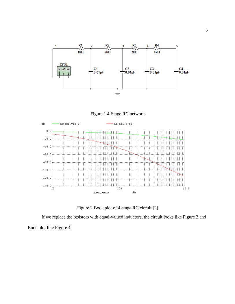
6
Figure 1 4-Stage RC network
Figure 2 Bode plot of 4-stage RC circuit [2]
If we replace the resistors with equal-valued inductors, the circuit looks like Figure 3 and
Bode plot like Figure 4.

7
Figure 3 4-stage LC circuit
Figure 4 Bode plot of 4-stage LC circuit [2]
It is evident from the above Bode plots that the poles and zeros from the real axis that are
transferred on to the imaginary axis can be seen quite significantly [2].

8
3.1.3 Active RC Circuit with Roots on RLHP
The active RC circuit should also be converted to an LC circuit so that the roots are
mapped onto the jω axis. The controlled-sources/voltage-controlled voltage source (VCVS),
current-controlled current source (CCCS), voltage-controlled current source (VCCS) and
current-controlled voltage source are the four components that make a circuit active. The VCVS
and CCCS are dimensionless. So, while transferring the RC circuit to an LC circuit, these two
components do not require any additional changes. We have two options to deal with VCCS and
CCVS: we can convert both VCCS and CCVS to one of the other two components. The second
method is modifying the trans-conductance Gm to Gm/s which is for voltage-controlled current
source and for current-controlled voltage source the trans-resistance rm must is modified to s*rm .
The first technique seems to be a suitable one because the circuit simulators do not accept
complex and frequency-dependent coefficients [2].
3.1.4 RL Circuit with Roots on RLHP
In order to extract roots for RL circuits both active and passive, the roots on the left half
of the real axis should be shifted onto the imaginary axis. All the changes are to be made just like
we did for the RC circuit. Here the resistor is replaced with a capacitor of same value. The active
components are also treated in the same way as mentioned above for the RC circuit.
3.1.5 RC and RL Circuits with Roots on RRHP
The above cases deal with the real roots on left-hand side. In order to find out the real
roots on right-hand side, change the signs of all capacitors if it is an RC circuit and change the
signs of all inductors if it is an RL circuit. Once the signs are changed, replace each resistor with

9
an equal-value inductor in an RC circuit (replace each resistor in an RL circuit with a capacitor
of equal value). Coming to the controlled sources, the VCCS and CCVS are changed to either a
VCVS or CCCS. Once these changes are made, the circuit is ready and its Bode plot is plotted.
We can observe the upward spikes and downward spikes which represent the poles and zeros
that are located on the right-hand side of the real axis [1]. Here when the sign of the capacitor or
inductor is changed the roots are mirrored, which means that when the sign of a capacitor is
changed in an RC circuit, the roots that lie on right part of real axis are shifted to the left part of
real axis. These roots are eventually transferred to the imaginary axis by following the previously
mentioned steps. Thus the roots are extracted when a sweeping sinusoidal signal is applied along
the imaginary axis. With this we have successfully gone through methods to extract all real-axis
roots for passive and active RC or RL circuits [1].
3.1.6 Roots that are Complex Conjugates Residing on the s-Plane and Real-axis Roots of RLC
Circuits
The technique mentioned in this session is suitable to extract roots that are complex
conjugates residing on s-plane and also real-axis roots of RLC circuits. Actually speaking, this
technique will be able extract all types of roots, including all the real-axis roots. So this can
replace all the previously mentioned techniques for extracting roots. Rather than trying an
algorithm to transfer the poles and zeros onto the imaginary axis, it was proposed to sweep the jω
axis [1].
Here we have to remember that the Bode plot has an upward peak when it comes across a
pole and a downward peak whenever it comes across a zero. It looks plain if it doesn’t have
either a pole or a zero. We already learned that poles on the imaginary axis can directly be

10
extracted by sweeping sinusoidal signal. The idea here is to move the imaginary axis so that the
roots fall on the imaginary axis and they get identified and extracted.
Let us assume a pair of complex poles located on s-plane, but not on the imaginary axis.
Now we make an s-plane transformation by moving the jω axis to meet the pair of complex poles
as shown in Figure 5.
Figure 5 S-plane transformation for the jω axis to meet the poles [1].
To apply this transformation, all we have to do is add a conductance in parallel with each
capacitor and add a resistance in series with each inductor [1]. But the problem is that we do not
know the exact value of the frequency where the poles or zeros are located in order to move the
jω axis. So we keep moving the imaginary axis in steps until it comes close or in contact with the
roots. The sweeping of this imaginary axis is done within the WinSpice implementation. All the
circuit transformations are implemented and tested using WinSpice.
Figure 6 represents the extraction of a pole through Bode plot by sweeping the jω axis.
We can observe from the multiple plots that the pole dominantly appears in one particular plot.
That is the plot obtained when the jω axis is at the nearest to the pole as depicted in Figure 6.

11
102
103
104
-40
-30
-20
-10
0
10
20
30
40
50
60
Figure 6 Bode plot of sweeping jω axis
3.2 3D Plots in MATLAB Using the System Transfer Function
Since a part of my work is to obtain a 3D plot which represents poles and zeros, I decided
MATLAB would be a suitable tool. As part of investigating previous works, I found out several
works directly in MATLAB which use the system transfer function for the s-plane plot and LTI
visualization [4]. The following plots represent the complex plane plot of a Butterworth filter and
an elliptic 5th-order complex plane plot. These are plotted in MATLAB using the transfer
function of the system. By looking at this work it is understood that MATLAB is a suitable tool
for obtaining a 3D Bode plot, which cannot be achieved through SPICE, as shown in Figures 7
and 8.

12
Figure 7 4th-order Butterworth filter complex plane plot [4]
Figure 8 Elliptic 5th-order filter complex plane plot [4]

CHAPTER 4
PROPOSAL
In this work two tasks are performed. The first one is generating an equivalent circuit of
MOSFET and using the equivalent circuit to replace the original MOSFET. Secondly, Bode plots
are expanded into three-dimensions in which the previously generated MOSFET equivalent
circuit is implemented. Two different tools are designed, one for calculating the model
components for an AC analysis equivalent circuit of MOSFET and the other one is to convert the
2D Bode plot into 3D Bode surface using MATLAB. Once the model components are generated
using model parameters, an equivalent circuit is generated to replace the MOSFET and the
circuit functionality still remains the same. All that needs to be done is simulate the generated
circuit in SPICE. For this purpose WinSpice3 has been used in this work. Once the circuit runs
fine in WinSpice3, it is made ready to be accessed in MATLAB. The results are then analyzed
using MATLAB. This algorithm involves the following steps:
Changes to be done to the given circuits to prepare it for plotting.
Writing a SPICE code for the circuit.
Creating a cell in MATLAB with the SPICE code.
Use MATLAB to create a .cir file and copy the SPICE code into it.
Run the .cir file in WinSpice3.
Write the output to .csv files which are accessible to MATLAB.
Use MATLAB to extract the parameters from the .csv files.
Create a 3D Bode plot using MATLAB.

14
Develop new algorithm to identify the inaccessible nodes in advanced analog circuits.
Both the tools are generated through Python programming. When the executable files are run,
they request input values which are required to generate certain outputs. The tools generate a
user interface where one types in the inputs. The first tool requests model parameters as inputs
and displays the values of the model components on the same interface where it requested inputs.
The second tool requests some information as well as the SPICE file as inputs and it
automatically creates a new MATLAB file executed to generate the Bode surface. This tool
mainly saves time and energy of the user.

CHAPTER 5
THEORY
5.1 Transfer Function
Transfer function is a mathematical representation of relation between input and output of
any black box model. Typically it is defined for determining the input vs output relationship of
linear time-invariant (LTI) systems with zero initial conditions. They are implemented in the
analysis for single-input/single-output systems where in general a frequency-dependent response
is required. It is expressed in terms of two polynomials: numerator and denominator
polynomials. It is denoted by H(s) and is given by:
where N(s) is the numerator polynomial and D(s) is the denominator polynomial. ‘s’ being the
complex variable, s = σ + jω.
Transfer function analysis is very useful in knowing the frequency response of any black
box. A test signal X(s) which is known is sent into any black box and the corresponding output
Y(s) can be calculated with the knowledge of the system transfer function H(s).
5.2 Poles and Zeros
The roots of the numerator polynomial N(s) are referred to as zeros and the roots of the
denominator polynomial D(s) as poles. Interpretation of zeros is that value of frequency where
the system transfer function becomes zero. And poles are the places where the system transfer

16
function tends to infinity, which is a discontinuity in the plot. For an example, let us consider the
following transfer function:
If we equate the numerator to zero, the roots a, b are called the zeros of the transfer
function. In other words, at a or b the function tends to zero. Similarly, c, d are the poles of the
transfer function, where the function tends to infinity.
5.3 Bode Plot
It represents the graph of a frequency response of a system. With either magnitude or
phase on the y-axis and a logarithmic frequency scale on the x-axis, there are two parts of a Bode
plot. The Bode magnitude plot as the name suggests is a graph of the magnitude response with
respect to frequency of the system. The Bode phase plot is the graph of the phase shift with
respect to frequency of the system.
As an example, let us consider the following transfer function and find its Bode plot
using MATLAB, which are shown in Figure 9.

17
Figure 9 Magnitude and phase Bode plots
5.4 Linear Circuit
An electronic circuit which has a sinusoidal input of frequency f and produces a
sinusoidal output of same frequency for any steady-state response is termed as a linear circuit.
The output should have the same frequency as input but it need not be in phase. A linear circuit
obeys superposition theorem. In a linear circuit the values of the components do not change with
varying voltage or current in the circuit. The significance of a linear circuit is that it processes
and amplifies signals without causing distortion. Fourier analysis and Laplace transform are the
techniques used to analyze linear circuits.

18
5.5 Non-linear Circuits
In a non-linear circuit, the circuit parameters are not constant and vary with respect to
voltage and current. A diode is an example of a non-linear element. The non-linear elements
cause distortion in electrical signals.
5.6 RC Low-pass Circuit
A first-order RC circuit is comprised of one resistor and one capacitor connected in
electrical series. Output can be taken either across R or C. Suppose we consider the case where
the output is taken across C; the transfer function is of the form:
If R = C = 1, then the Bode plot looks like Figure 10.
-40
-30
-20
-10
0
Magnitude (
dB
)
10-2
10-1
100
101
102
-90
-45
0
Phase (
deg)
Bode Diagram
Frequency (rad/s)
Figure 10 RC low-pass Bode plot

19
5.7 RL High-pass Circuit
A first-order RL circuit is comprised of one resistor and one inductor connected in
electrical series. Output can be taken either across R or L. Suppose we consider the case where
the output is taken across L; the transfer function is of the form:
If R = L = 1, then the Bode plot looks like Figure 11.
-50
-40
-30
-20
-10
0
Magnitude (
dB
)
10-2
10-1
100
101
102
0
45
90
Phase (
deg)
Bode Diagram
Frequency (rad/s)
Figure 11 RL high-pass Bode plot
5.8 SPICE
SPICE stands for Simulation Program with Integrated Circuit Emphasis. It is an analog
electronic simulator available in open source. It uses nodal analysis for constructing the circuit
equations. It was first developed at University of California, Berkeley, at the Electronics
Research Laboratory. It inspired and led the way to many other simulation programs with coding
style remaining almost the same. The different types of SPICE available are:

20
5.8.1 P-SPICE
P-SPICE is a short form for Personal Simulation Program with Integrated Circuit
Emphasis. It is a modified version of SPICE and was commercialized in 1984 by MicroSim.
Later in 1998 MicroSim was purchased by OrCAD. The upgraded version of P-SPICE is OrCAD
EE. It includes more options like viewing, waveform recording, curve fitting and analysis.
5.8.2 LT-SPICE
LT-SPICE is a SPICE simulator of electronic circuits which was produced by Linear
Technology, a semiconductor manufacturer. The LT-SPICE is a freeware software available for
use at no cost. The simulation of switching regulators is fastened. It provides over 1100 macro
models of LTCs. It allows unlimited number of nodes. LT-SPICE is used in digital electronics,
power electronics, radio frequency electronics and other fields. It is provided with advanced
simulation and analysis options; however, it cannot simulate complex digital logics.
5.8.3 H-SPICE
The H-SPICE is an accurate circuit simulator which offers device models with state-of
the-art analysis and simulation algorithms. It precisely predicts the functionality, power
consumption, timing and yield of the electronic circuits.
5.8.4 WinSpice
WinSpice is a variant of Berkeley SPICE3F4 which is compatible with Win 32 systems.
It can generate waveform plots into windows and contains a very powerful scripting language. It

21
does not contain a schematic editor by itself. It works from all the Windows versions from
Win95 to date.
5.8.5 Multisim
Multisim is maintained by National Instruments and is mostly used for educational
purposes. Multisim is a part of a suite of circuit design software. It includes integrated import/
export feature to the PCB layout software in the suite.
5.9 SPICE Simulator
A flow chart showing the execution of SPICE program is shown in Figure 12.
Figure 12 Flow diagram of main SPICE program

22
The SPICE simulator considers the input circuit and determines the DC operating point
as an initial step. Later it creates linear models for non-linear components such as diodes and
transistors. Next step is an important step which is the nodal analysis part. It comprises creating
the nodal equations and solving them for voltage. For non-linear circuits the resulting set of the
linear equations are solved until they reach a fixed point. It may take many iterations before the
convergence occurs. The time step incrementing along with the other steps is implemented for
the transient analysis part.
5.10 Types of Analysis
There are three main types of analysis which SPICE performs. Apart from those it also
performs extended analysis like Fourier, sensitivity, noise, etc.
5.10.1 DC Analysis
In SPICE the DC analysis part is performed to determine the DC operating point. The DC
operating point is calculated by neglecting all the energy storage elements, the inductors
shortened and the capacitors open circuited. The .DC, .OP and .TF are the control lines that
specify the DC analysis. An operating point is an initial solution to the transient analysis. The
DC analysis is also performed prior to the AC analysis in order to determine the linearized
models for non-linear devices. The DC sweep analysis performs the DC analysis multiple
number of times as you sweep a component value across a selected range. Performing DC
analysis for linear circuits is the simplest part of the analysis. All it needs to do is to load the
nodal matrix and calculate the voltage by solving nodal equations. But for non-linear circuit, it
has to create linear models for the non-linear components, which doesn’t give the exact solution.
The exact solution is found out iteratively by calculating the operating point, creating the

23
equivalent linear circuit and the nodal matrix and finally solving the nodal matrix for voltages. It
will again choose a new operating point depending on the voltages and the loop begins again.
The loop is stopped when the changes in circuit voltages and currents are minimum and reached
the limit. As a part of solution to the DC analysis it can also generate the DC small signal value
and also the input and output resistances.
5.10.2 AC Analysis
The AC analysis part of SPICE generates the AC output variables as a function of
frequency. The operating point is determined first, after which the linearized small-signal models
are generated for non-linear components. For all the requested frequencies the nodal matrices are
computed and solved for the nodal voltages. For an AC analysis the desired output is generally a
transfer function.
5.10.3 Transient Analysis
The transient analysis generates the output variables as a function of time. The first step
is usually finding the DC operating point. The time interval for transient analysis is specified on
.TRAN control line. It also adjusts the time step. Whenever the circuit voltages and currents
change randomly, the time step is reduced so that the accuracy is increased. And if there is not
much change in the circuit voltages and currents, the time step is increased to reduce the
simulation times.

24
5.11 SPICE Components and Syntax
This section lists the components and syntax that are used in building the example
circuits. WinSpice3 is used.
5.11.1 Resistor
A resistor is represented by the letter ‘R’. A simple resistor is used in all examples.
The general form of a simple resistor is as follows:
RXXXXXXX N1 N2 VALUE
N1 and N2 are the node numbers between which the resistor is placed. VALUE is the resistance
in ohms.
Example:
R1 2 3 1k
Here R1 is the resistor with 1000 ohms resistance placed between the nodes 2 and 3.
Other forms:
RXXXXXXX N1 N2 R=<expression>
Example:
R2 1 4 R=1000+log (v (2))
This means that the value of R could also be given in the form of an expression rather than
directly giving the value.

25
5.11.2 Capacitors
A capacitor is represented by the letter ‘C’. General form of a simple capacitor:
CXXXXXXX N+ N- VALUE
CXXXXXXX N+ N- C=<expression>
N+ and N- are the positive and negative nodes of the capacitor respectively. VALUE is
capacitance in farads.
Examples:
CG 12 0 1u
Cgs 10 3 C = 20u
CG is a capacitor between nodes 12 and 0 with 1u farad capacitance.
5.11.3 Inductors
An inductor is represented by the letter ‘L’. General form:
LXXXXXXX N+ N- VALUE
LXXXXXXX N+ N- L =<expression>
N+ and N- are positive and negative nodes of the inductor respectively. VALUE is the
inductance in henries.
Examples:

26
Lf 23 35 1mH
Lf is an inductor between the nodes 23 and 35 with an inductance value of 1m henry.
5.11.4 Voltage and Current Sources
The voltage source is represented by the letter ‘V’and the current source is represented by
the letter ‘I’. General form:
VXXXXXXX N+ N- <<DC> DC/TRAN VALUE> <AC > <ACMAG <ACPHASE>>
IYYYYYYY N+ N- <<DC> DC/TRAN VALUE> <AC > <ACMAG <ACPHASE>>
N+ and N- are the positive and negative nodes of the voltage source. It is assumed that positive
current flows from the positive node through the source and into the negative node. The
DC/TRAN is the DC and transient analysis value of the source. ACMAG and ACPHASE are the
AC magnitude and AC phase respectively.
Examples:
Vdd 1 0 DC 5
Vin 10 1 DC 0.5 AC 1
If ACMAG is not specified, it is assumed to be unity and if ACPHASE is not specified it is
assumed as zero.

27
5.11.5 Voltage-Controlled Voltage Source
There are two types of controlled sources: linear and non-linear. The linear voltage-
controlled voltage source is represented by the letter ‘E’. General form:
EXXXXXXX N+ N- NC+ NC- GAIN
N+ and N- are the positive and negative nodes respectively. NC+ and NC- represent the positive
and negative controlling nodes. GAIN is the voltage gain.
Example:
E1 4 5 12 13 3.0
The component E1 is between nodes 4 and 5 and it is controlled by the voltage across the nodes
12 and 13 with a voltage gain of 3.0.
The general form of the non-linear voltage controlled voltage source is as follows:
EXXXXXXX N+ N- <POLY (ND) > NC1+ NC1- …. P0 <P1…> <IC= …>
N+ and N- are the positive and negative nodes of the source. If the source is multi-dimensional,
then POLY(ND) is specified and ND is the number of dimensions. NC1+, NC1-, … are the
controlling nodes. If the source is multi-dimension, there will be more than two controlling
nodes. P0, P1, . . . Pn are the polynomial coefficients.
5.11.6 Voltage-Controlled Current Source
It is denoted by the letter ‘G’. The general form of a linear voltage controlled current
source is

28
GXXXXXXX N+ N- NC+ NC- VALUE
N+ and N- are the positive and negative nodes of the source respectively. NC+ and NC- are the
controlling nodes, between which the controlling voltage is present. VALUE is the trans-
conductance in mhos.
5.11.7 Current-Controlled Current Source
It is represented by the letter ‘F’. The general form of a linear current-controlled current
source is as follows:
FXXXXXXX N+ N- VNAM GAIN
N+ and N_ are positive and negative nodes of the source. Current flows from the positive node
through the source and into the negative node. VNAM represents the voltage source through
which the controlling current flows. GAIN denotes the current gain.
5.11.8 Current-Controlled Voltage Source
It is represented by the letter ‘H’. The general form of a linear current-controlled voltage
source is as follows:
HXXXXXXX N+ N- VNAM VALUE
N+, N- and VNAM represent positive node, negative node and the name of voltage source
through which controlling current flows respectively. VALUE is the trans-resistance in ohms.

29
5.11.9 MOSFET
This component is represented by the letter ‘M’. General form:
MXXXXXXX ND NG NS NB MNAME <L=VAL> <W=VAL> <AD=VAL> <AS=VAL>
+ <PD=VAL> <PS=VAL> <NRD=VAL> <NRS=VAL> <OFF>
+ <IC=VDS, VGS, VBS> <TEMP=T>
ND, NG, NS and NB represent the nodes drain, gate, source and bulk respectively. MNAME is
the model name. L and W are the length and width in meters. AD and AS are the drain area and
source diffusions in meters2. PD and PS are the junction perimeters of the drain and the source.
NRD and NRS are the number of squares of drain and source diffusions. OFF denotes the initial
condition for DC analysis.
5.11.10 BJT
It is represented by the letter ‘Q’. General form:
QXXXXXXX NC NB NE <NS> MNAME <AREA> <OFF> <IC=VBE, VCE> <TEMP=T>
NC, NB, NE and NS are the nodes representing the collector, base, emitter and substrate
respectively. MNAME is the model name, AREA is the area factor and OFF indicates an initial
condition for the DC analysis.
5.12 MATLAB
MATLAB (Matrix Laboratories) is a proprietary software developed and maintained by
Math Works. It allows matrix manipulations, plotting of functions in 2D and 3D, implementation

30
of algorithms and interfacing codes written in other programming languages. It finds its use in
various diversified fields like engineering, science and economics. It is a scripting language but
one can also develop functions. There are various toolboxes present to support various aspects,
like signal processing toolbox, communication toolbox, statistical toolbox, image processing
toolbox, etc. The UI consists of four major sections, namely, command window, editor window,
current folder window and workspace window. The following is the list of all the commands that
are part of this thesis work.
5.12.1 clear
This command is used in conjunction with item type ‘all’ to clear all the items in the
workspace. It also frees up all of the system memory.
Syntax:
>> clear name1 name2 … nameN
>> clear itemType
5.12.2 close
This command is used to close various things like objects, figures, connections, etc. But it
is primarily used to close all the windows except for the main window.
Syntax:
>> close all

31
5.12.3 clc
This command stands for “clear command window.” It is generally placed at the
beginning of the script to make clear all the recent commands on the command window.
5.12.4 size()
This is a function which is used to find the size of the object array parameter that is being
passed to it. This function is part of the parallel computing toolbox. This function returns a size
of a single-dimensional array, multi-dimensional array and size along particular dimension(s).
Syntax:
>> d = size(object)
>> [m1 ,m2, …,mn] = size(object)
>> m = size(object, dimension)
5.12.5 figure
This function is used to create a new figure graphics object. Figure objects are referred to
as individual windows on the screen. This function automatically assigns the default properties to
the object and raises it above all other figures on the screen.
Syntax:
>> figure
>> figure(‘PropertyName’, propertyvalue,…)

32
5.12.6 label
This command is prefixed with corresponding axis names to name them accordingly.
They are named as xlabel, ylabel and zlabel. The name of the axis is named after the string that is
passed to it.
Syntax:
>> xlabel(str)
>> ylabel(str, Name, Value)
5.12.7 surfc
This command is used to create a contour plot under the 3D shaded surface. When the
axes are passed into it, generally the third value is for the color data and surface height, whereas
the first and second values are used to form the components of the surface. Also, if the size of x-
axis is m and the size of y-axis is n, z should be of the size of m*n.
Syntax:
>> surfc(Z)
>> surfc(X,Y,Z)
>>>surfc(X,Y,Z,C)
where C defines the color.

33
5.12.8 semilogx
This function is used to plot data as logarithmic scales for x-axis. By default this function
creates a linear plot for y-axis and a base-10 log scale for the x-axis. It ignores the imaginary
components.
Syntax:
>> semilogx(Y)
>> semilogx(X1,Y1,...)
5.12.9 grid
This function is used to plot the grid lines for 2D and 3D plots.
Syntax:
>> grid on
>> grid off
5.12.10 hold
This function is used to retain the current graph when adding new graphs to the plot.
Syntax:
>> hold on
>> hold all

34
5.12.11 fopen
This command is used to open a particular file or to obtain the information about open
files. This function returns an integer file identifier which is greater than or equal to 3. MATLAB
reserves 0, 1 and 2 for standard input, output and error respectively. You can choose the file
format according to your need. For the thesis purpose we made use of .cir file extension.
Syntax:
>> fileID = fopen(file-name)
>> fileID = fopen(filename, permission, machinefmt, encodingIn)
5.12.12 fprintf
This function is used to write data into text file. By default this function takes three
parameters. A file identifier, format specification and elements of array(s) are passed as
parameters.
Syntax:
>> fprintf(fileId, formatSpec, A1, A2,…,An)
5.12.13 fclose
This function is used to close one or multiple open files. Generally, fopen has to be
followed by fclose because any file that is opened has to be closed.
Syntax:

35
>> fclose(fileId)
>> fclose(‘all’)
5.12.14 textscan
This function is used to read formatted data from a text file or string. This can take a file
identifier, format specifiers, number of times to check for the format specifier, etc.
Syntax:
>> textscan(fileId,formatSpec,N)
5.13 Python
Python is a high-level, general-purpose programming language. It is also an object-
oriented programming language similar to C++, JAVA, etc. But it differs from other
programming language in its syntax. The syntax facilitates the programmers to express their
concepts in fewer lines of code. Python is very powerful programming which supports multi-
paradigms which include objected-oriented, imperative and procedural or functional
programming. It also features a dynamic-type system and automatic memory management. Many
operating systems have various Python interpreters. By using wide variety of third-party tools
like Py2exe, Python code can be packaged into standalone executable application, which is
similar to what has been implemented in this project. Rather than building all the desired
functionalities into the core of the languages, Python was made highly extensible. Python has
been designed to be a highly readable language. It is intended to use common English keywords
in place of punctuation, which is generally the case in other programming language. It uses

36
whitespace indentation instead of curly braces to separate blocks of code. This feature is called
off-side rule.
Python consists of a large standard library which is one of the Python’s greatest strengths.
These libraries provide tools that can be used to perform various tasks. Various modules that can
support file system access, graphical user interface creation, database connectivity, random
number generation, etc., are available in the open community. There are various integrated
development environments (IDEs) available which can increase the productivity of
programmers. Various commands used as part of this thesis work are explained in the following
section. Naming conventions for variables and methods have a predefined set of rules, which is
generally called camel-case convention.
5.13.1 import
This command is used to import various modules to the program. Different predefined
modules have various common or desired functions built in. We can use those functions by
importing the module, or package in terms of Java, into the programs. Always the code should
start with the import statements.
Syntax:
import os,sys
import tkMessageBox
5.13.2 def
In Python, when we want to create a new function, we make use of the ‘def’ command
followed by function name and parentheses. These functions can also have parameters passed

37
into them. These parameters have positional behavior; hence, they have to be passed in order of
definition. As mentioned earlier, in Python any block of code should be indented properly.
Syntax:
def functionName(parameters):
“function body”
return [experession];
5.13.3 with
This command is very handy when dealing with opening and closing files. This command
is very useful if a block of code needs to be executed which is in between two related executable
pairs of operations.
Syntax:
with open(‘output.txt’, ‘w’) as filename:
filename.write(“ String”)
5.13.4 print
To perform the standard output, which is printing in the screen, we make use of ‘print’
command. In previous versions of Python, the text needed to be just embedded within double
quotes, but latest version also requires us to enclose it inside parentheses.
Syntax:
print “Hello world!”
print (“Hello world!”)

38
5.14 AC Analysis Equivalent Models for MOSFET
For dealing with the non-linear components such as MOSFETs or BJTs, these
components should be replaced with their linearized AC analysis models in order to obtain poles
and zeros through the Bode plot.
5.14.1 MOSET Models
In general a model refers to a simplified and idealized understanding of physical terms.
Models help a lot in performing SPICE simulations. Modifications can be made to the ideal
model to mimic the real-life scenario. MOSFET has various models differentiated in terms of
parameters, namely, CAPOP and ACM model parameters. CAPOP specifies the gate
capacitances and it is often referred to as capacitance model. ACM stands for “area calculation
method” and selects the correct diode model for the MOSFET’s bulk diode and is it referred to
as Diode model. Each of these sub-models can be used in specific simulations to obtain
distinguished results [5].
MOSFET models can be broadly classified into p-channel and n-channel models. These
are further classified according to level, like Level 1 or Level 50. Level 1 models have low
simulation times and high accuracy in terms of timing calculations. Hence, this model is most
suited for analysis of large digital circuits. Level 6 IDS and BSIM models (Level 13, 39 or 49)
are used for analog data acquisition circuitry. These models offer better precision when dealing
with analog circuits. BSIM models account for variations in geometric parameters. These BSIM
models are best suited for modelling of MOS capacitor effects as it is based on MOS charge
conservation model. Level 27 SOSFET (silicon on sapphire) can be used for photocurrent
effects. Level 5 and Level 38 are used for depletion MOSFETs. Level 2 can be used to account

39
for bulk charge effect on current. Level 3 is better than the above model and offers optimized
simulation time and accuracy. Level 6 can be used to implement ion-implanted devices [5].
5.14.2 Selecting Models
MOSFET statement often specifies the type of the device, either p- or n-channel device,
its level and a number of user-selectable model parameters. For example:
M3 3 2 1 0 PCH <parameters>
.MODEL PCH PMOS LEVEL=13 <parameters>
This example specifies a PMOS with a reference name of PCH. Also it specifies that the model
belongs to Level 13 BSIM model. Table 1 specifies the various levels and their names.
Table 1 MOSFET Level and corresponding model description [5]
LEVEL MOSFET Model Description
1 Schichman-Hodges model
2 MOS2 Grove-Frohman model (SPICE 2G)
3 MOS3 empirical model (SPICE 2G)
4 Grove-Frohman: Level 2 model
5 AMI-ASPEC depletion and enhancement
6 Lattin-Jenkins-Grove (ASPEC style)
7 Lattin-Jenkins-Grove (SPICE style)
8 Advanced Level 2 model
9 AMD model (not available for Windows OS)
10 AMD model (not available for Windows OS)
11 Fluke-Mosaid model
(Continued on following page)
40
Table 1. Continued.
LEVEL MOSFET Model Description
12 CAMOS model (GTE style)
13 BSIM model
14 Siemens level 4 (not available for Windows)
15 User-defined model based in level 3
16 Not used
17 Cypress model (not available for Windows)
18 Sierra 1 (not available for Windows)
19 Dallas Semiconductor model
20 GE-CRD FRANZ
21 STC-ITT
22 CASMOS (GEC style)
23 Siliconix
24 GE-Intersil advanced
25 CASMOS (Rutherford)
26 Sierra 2
27 SOSFET
28 BSIM derivative; Meta-software proprietary
29 Not used
30 VTI
31 Motorola
32 AMD
33 National semiconductor
34 EPFL (not used)
35 Siemens
36 Sharp
37 TI
38 IDS: Cypress depletion model
39 BSIM2
41 TI Analog
46 SGS-Thomson MOS LEVEL 3
47 BSIM3 Version 2.0
(Continued on following page)

41
Table 1. Continued.
LEVEL MOSFET Model Description
49 BSIM3 Version 3 (Enhanced)
50 Philips MOS9
53 BSIM3 Version 3 (Berkeley)
54 UC Berkeley BSIM4 Model
55 EPFL-EKV Model Ver 2.6, R 11
57 UC Berkeley BSIM3_SOI MOSFET Model Ver 2.0.1
58 University of Florida SOI Model Ver 4.5
59 UC Berkeley BSIM-501 FD Model
61 RPI a Si TFT Model
62 RPI Poli-Si TFT Model
63 Philips MOS11 Model
64 STARC HiSIM Model
65 SSIMOI Model
66 HSPICE HVMOS Model
70 BSIMO14.0 Model
71 TFT Model
CAPOP, the MOSFET capacitance model parameter, differentiates various gate
capacitance models depending on the value of CAPOP. Various capacitor models are used to
model the MOS gate capacitance, in particular, the gate-to-drain capacitance, gate-to-source
capacitance or gate-to-bulk capacitance. Some models are specific to certain DC models.
ACM, which controls the geometry of source and drain diffusions, is another model
parameter which helps in modelling of bulk-to-source and bulk-to-drain diodes in the model. The
diode model consists of diffusion resistance, capacitance and DC currents to the substrate. The

42
W/L values which specify the width and length of gate play a crucial role in modelling the
MOSFET.
Apart from the above parameters, specific control options, set in .OPTIONS statement,
are used to provide more details inside the model. These options can be seen in Table 2.
Table 2 Options and their functionalities [5]
OPTIONS Functionality
MBYPASS BYPASS tolerance multiplier
DEFAD Default drain diode area
OPTIONS Functionality
DEFAS Default source diode area
DEFL Default channel length
DEFW Default channel width
DEFNRD Default number of squares for drain resistor
DEFNRS Default number of squares for source resistor
DEFPD Default drain diode periphery
DEFPS Default source diode periphery
GMIN PN junction parallel transient conductance
GMINDC PN junction parallel DC conductance
SCALE Element scaling factor
SCALEM Model scaling factor
WL Change length-width
These default values can be overridden by specifying AD, AS, L, etc.

43
5.14.3 MOSFET Element Syntax
The general format of MOSFET element syntax is as follows:
Mxxx nd ng ns <nb> mname <L=val> <W=val> <AD=val> <AS=val> <PD=val> <PS=val> +
<NRD=val> <NRS=val> <RDC=val> <RSC=val> <OFF> <IC=vds, vgs, vbs> <M=val> +
<DTEMP=vale> <GEO=val> <DELVTO=val>…
where Mxxx = MOSFET element name. Name must being with ‘M’.
Ng = gate terminal node name
Ns = source terminal node name
Nb = bulk terminal node name
Nd = drain terminal node name
Mname = model name reference
L = channel length
W = channel width
AD = drain diffusion area
AS = source diffusion area
PD = perimeter of drain junction
PS = perimeter of source junction
NRD = number of squares of drain diffusion for resistance calculations

44
NRS = number of squares of source diffusion for resistance calculations
RDC = additional drain resistance due to contact resistance
RSC = additional source resistance due to contact resistance
OFF = sets the initial condition to OFF for this element in the DC analysis
M = multiple device option
vbs = initial condition for the voltage across the external bulk and source terminals
vds = initial condition for the voltage across the external drain and source terminals
vgs = initial condition for the voltage across the external gate and source terminals
DTEMP = device temperature difference from circuit temperature
GEO = source/drain sharing selector for ACM = 3
DELVTO = zero-bias threshold voltage shift
val = value [5]
5.14.4 BSIM Model
BSIM stands for Berkeley short channel IGFET. The SPICE 2G.6 model has been used
by HSPICE in their Level 13 MOSFET. The model is predicated on the device physics of small-
geometry MOS transistors. Some of the Level 13 model parameters are given in the Table 3.
NMOS conventions are specified for all Level 13 parameters, even for PMOS.

45
Table 3 BSIM Level 13 model parameters [5]
NAME Default value
CGBO 2.0e-10 F/m
CGDO 1.50E-09
CGSO 1.5e-9 F/m
MUS 600 cm2/(V-s)
PHI0 0.7 V
TREF 25.0 oC
TOX 0.02 um
K1 0.5 V ½
VDDM 50V
VFB -0.3V
NAME Default value
X3MS 5.0 cm2/ (V2. S)
XPART 1
CJSW 0.0 F/m
CJ 4.5e-5 F/m2
MJ 0.5
5.14.5 Level 13 Model Equations
L and W are added at the start of the name of an electrical parameter in a transistor in
order to denote the channel length and channel width sensitivity factors of the parameter.
A= A0+LA. ((1/Leff)-1/LREFeff)) + WA. ((1/Weff)-(1/WREFeff))
LA and WA will have the units of A0 times microns.

46
The effective model parameters are represented by the parameter name preceded by the
letter ‘z’, all in lower case.
Example: If VFB is the model parameter, the effective model parameter after changing the size
of the device is given as:
Zvfb = VFB0+ LVFB. ((1/Leff)-(1/LREFeff)) + WVFB. ((1/Weff)-(1/WREFeff))
Calculating the effective length and width actually depends on the model parameters
specified. If DL0 and DW0 are specified, then:
Leff = Lscaled. LMLT – DL0
LREFeff = LREFscaled. LMLT – DL0
Weff = Wscaled. WMLT – DW0
WREFeff = WREFscaled. WMLT – DW0
If LD and WD are specified
Leff = Lscaled. LMLT + LDscaled – 2
LREFeff = LREFscaled. LMLT + LDscaled – 2
Weff = Wscaled. WMLT + WDscaled -2
WREFeff = WREFscaled. WMLT + XWscaled – 2
Since the thesis requires the transistor to operate in saturation region, we concentrate on
the saturation region equations:

47
Ids for saturation region vds>vdsat
Ids = β/ (2. Body. Arg).(vgs – vth)2
The value of β is calculated by
β = µeff. COX. Weff/Leff
µeff = µo/( 1+xµ0.(Vgs – Vth))
To calculate µo carrier mobility, quadratic interpolation is used.
µo|vds=0 = MUZ- zx2mz ɸvsb
µo|vds=VDDM = zmus – zx2ms ɸvsb
The body factor is calculated by:
Body = 1 + (g * zk1/ 2* (zphi + vsb)1/2)
The value of g in the body factor is calculated by:
g = 1 – 1/(1.744+0.8364 *(zphi + vsb))
The arg term in the saturation region is calculated by:
arg = ½ * ( 1+ vc + (1+2*vc)1/2)
where vc = xu1 * (vgs – vth)/ body
xu1 = zu1 – zx2u1
Threshold voltage:

48
Vth = zvfb + zphi + gamma *(zphi +vsb)1/2- xeta
where gamma = zk1 – zk2
Xeta = zeta – zx2e
Resistors and capacitors:
C = COX . Leff. Weff + 2. CAPSW. (Leff+Weff)
The Level 13 model is a charge conservation capacitance model. The equations to obtain
the charge stored:
Vtho = zvfb + zphi + zk1* (zphi + vsb)1/2
Cap = COX. Leff. Weff
The charge conserved in saturation region for different values of XPART:
50/50 channel-charge partitioning for drain and source XPART = 0.5.

49
Qs = Qd
40/60 channel-charge partitioning for drain and source, XPART = 0.
0/100 channel-charge partitioning for drain and source, XPART=1.
Qd = 0
Qs = -Qg – Qb [5].
Now let us investigate about a more recent one, the Level 54 BSIM 4.0 model. This model
has many improvements over the previously discussed Level 13.
50
It is an accurate model for both high-speed digital and high-frequency analog
applications.
It has a consistent AC model that accounts for the NQS effect in both trans-conductances
and capacitances.
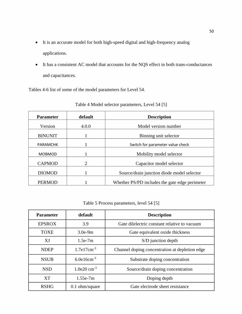
Tables 4-6 list of some of the model parameters for Level 54.
Table 4 Model selector parameters, Level 54 [5]
Parameter default Description
Version 4.0.0 Model version number
BINUNIT 1 Binning unit selector
PARAMCHK 1 Switch for parameter value check
MOBMOD 1 Mobility model selector
CAPMOD 2 Capacitor model selector
DIOMOD 1 Source/drain junction diode model selector
PERMOD 1 Whether PS/PD includes the gate edge perimeter
Table 5 Process parameters, level 54 [5]
Parameter default Description
EPSROX 3.9 Gate dilelectric constant relative to vacuum
TOXE 3.0e-9m Gate equivalent oxide thickness
XJ 1.5e-7m S/D junction depth
NDEP 1.7e17cm-3 Channel doping concentration at depletion edge
NSUB 6.0e16cm-3 Substrate doping concentration
NSD 1.0e20 cm-3 Source/drain doping concentration
XT 1.55e-7m Doping depth
RSHG 0.1 ohm/square Gate electrode sheet resistance

51
Table 6 Basic model parameters, level 54 [5]
Parameter default Description
VTHO 0.7v (NMOS)
Threshold voltage at Vbs=0 -0.7V (PMOS)
VFB -1.0V Flat band voltage PHIN
K1 0.5V1/2 First order body bias coefficient
K3 80 Narrow width coefficient
W0 2.5e-6m Narrow width parameter
LPE0 1.7e-7m Lateral non uniform doping parameter
VBM -3.0v Maximum applied body bias in VTH0 calculation
DVT0 2.2 First coefficient of short channel effect on Vth
DVT1 0.53 Second coefficient of short channel effect on Vth
DVT1W 5.3e6m-1 Second coefficient of narrow width effect on Vth for
small channel length
DVT2W -0.032v-1 Body-bias coefficient of narrow width effect for small
channel length
U0
0.067m2/Vs -
NMOS Low- field mobility
0.025m2/Vs -
PMOS
UA 1e-15m/V Coefficient of first order mobility degradation due to
vertical field
UB 1e-19m2/V2 Coefficient of second-order mobility degradation due
to vertical field
UC -0.0465e-9m/V2 Coefficient of mobility degradation due to body-bias
effect
VSAT 8.0e4m/s Saturation velocity
KETA -0.047V-1 Body-bias coefficient of bulk charge effect
WINT 5.00E-09 Channel width offset parameter
(Continued on following page)

52
Table 6. Continued.
Parameter default Description
LINT 1.20E-08 Channel length offset parameter
CDSC 2.4e-4F/m2
Coupling capacitance between source/drain and
channel
PCLM 1.3 Channel length modulation parameter
CDSC 2.4e-4F/m2
Coupling capacitance between source/drain and
channel
PCLM 1.3 Channel length modulation parameter
5.14.6 MOSFET Equivalent Circuits
WinSpice3 employs three equivalent circuit models for analysis for MOSFET, namely:
DC, transient and AC and noise equivalent circuits. The components that go into these various
circuits differentiate the equivalent models. The equivalent DC sweep circuit is similar to
transient analysis circuit except for the capacitances are not included. DC drain-to-source current
is the basic component used in DC equivalent circuit. For AC and noise analysis, the actual
drain-to-source current (ids) is not used. In place of ids, the model used the partials of ids with
respect to vgs, vds and vbs. The names of these partials are: trans-conductance, conductance and
bulk trans-conductance.
Trans-conductance gm =
Conductance gds =
Bulk Conductance gmbs =

53
The ids equation describes the DC effects alone. The gate capacitance and source and
drain diodes effects are dealt with separately from ids equations. Also the impact ionization
equations are considered separately from DC ids equation.
Figures 13, 14 and 15 show the equivalent circuits for MOSFET transient analysis, AC
analysis and AC noise analysis respectively.
Figure 13 MOSFET transient analysis equivalent circuit [5]
Figure 14 MOSFET AC analysis equivalent circuit [5]

54
Figure 15 MOSFET AC noise analysis equivalent circuit [5]
5.14.7 MOS Gate Capacitance Models
Capacitance model parameters can be used in conjunction with all the MOSFET model
statements. Various capacitances parameters are CGDO (gate-to-drain), CGSO (gate-to-source)
and CGBO (gate-to-bulk). The parameter that is used to make a capacitance model selection is
CAPOP. Some of the models are only related to specific DC models, whereas others are
designed as general and can be used for any DC model.
When we have two terminals 1 and 2 with charges q1 and q2 (q1 = -q2) and voltages v1
and v2, the effective capacitance between these two nodes is given by C = dq/dV, where dq = q1
– q2 and dV = v1 – v2. But for a four-terminal capacitor, the algebraic sum of all the charges is
zero and also they can depend on the voltage differences or otherwise arbitrary functions. So for
three independent charges q1, q2 and q3 there are functions of three independent voltages v14,
v24 and v34. These make up the nine derivatives required to describe the small-signal

55
characteristics. But it is convenient to consider four charges as functions of four different
voltages, the derivatives of which form the 4X4 matrix, dqi/dVj, i = 1,.4, j = 1,.4. So to find the
current into a particular terminal which is a result of terminal voltage applied to that node with
respect to reference node, we make use of dqi/dVj function multiplied with 2*pi*frequency [5].
In order to find the junction capacitances it is very easy to use this matrix. The diagonal
matrix entries are the terminal input capacitances and the off-diagonal entries are the negative of
the trans-capacitances [5].
5.14.8 MOS Capacitances
A general MOSFET device with four terminals as Drain (D), Gate (G), Source (S) and
Bulk (B) has the following three capacitances associated with it:
CGG (Input capacitance) =
CGD (Miller feedback capacitance) = -
CDG (Miller feedthrough capacitance) = -
These capacitances can be derived directly from the 4X4 matrix of capacitances
discussed above. Also there is a difference between CGD and CDG. CGD represents a flow of
current from the gate due to a change in drain voltage. And CDG represents a capacitive current
flowing out of drain due to change in gate voltage. Figure 16 shows the various capacitances
associated with the MOSFET device.

56
Figure 16 MOSFET capacitances [5]
To elucidate how CGD and CDG are not equal, the following example presents a
simplified model with no bulk charge, with gate charge as a function of gate-to-source voltage
only.
qG = q(vgs)
qS = - 0.5. q(vgs)
qD = - 0.5. q(vgs)
qB = 0
CGD = - = 0
CDG = - = 0.5 .
Hence it is obvious that both CGD and CDG are different. Also there are six capacitances
that can be extracted in the operating point printout:
cdtot

57
cgtot
cstot
cbtot
cgs
cgd -
These capacitances have embedded in themselves all other capacitances, namely, gate-
drain, gate-source, and gate-bulk overlap capacitances, also drain-bulk and source-bulk diode
capacitances. For not well-defined models, the printout quantities are as follows:
cdtot cgd+cbd
cgtot cgs+cgd+cgb
cstot cgs+csb
cbtot cgb+csb+cdb
cgs cgs
cgd cgd
Gate-Bulk Capacitance (cgb)
Accumulation, vgs <= vfb – vsb

58
cgb = cap = COXscaled. Weff. Leff
Depletion, vgs <= vth
cgs =
Inversion, vgs > vth
cgb =
Gate-Source Capacitance (cgs)
Low vds (vds<0.1)
Accumulation, vgs < vth – CF1
cgs = CF5. cap
Depletion, vgs <= vth + CF2 – CF1
cgs = CF5. cap.
Strong Inversion, vgs > vth + max(CF2 – CF1, CF3 . vds) UPDATE = 0
Strong Inversion, vgs > vth + CF2 – CF1, UPDATE = 1
cgs = CF5. cap. {1 – [
High vds (vds >= 0.1)

59
Accumulation, vgs < vth – CF1
cgs = CF5. cap
Weak Inversion, vgs < vth + CF2 – CF1
cgs = CF5. cap. max( )
Saturation Region, vgs < vth + CF3 . vds
cgs = CF5. cap
Linear Region, vgs > vth + CF3 . vds
cgs = CF5. cap.
Gate-Drain Capacitance (cgd)
Low vds, (vds < 0.1)
Accumulation, vgs <= vth – CF1
cgd = CF5. cap
Weak Inversion, vgs < vth + CF2 – CF1
cgd = CF5.cap.
Strong Inversion, vgs >= vth + CF2 – CF1

60
cgd = CF5. cap.
High vds (vds > 0.1)
Accumulation, vgs <= vth – CF1
cgd = CF5. cap
Saturation Region, vgs <= vth + CF3. Vds
cgd = CF5. cap
Linear Region, vgs > vth + CF3. Vds
cgd = CF5. cap. . [5]
Rd ={RDWMIN+RDW.[-PRWB.Vbd+1/(1+PRWG.(Vgd-Vfbsd))]}/[(1e6.Weff).NF]
Rs ={RSWMIN+RSW.[-PRWB.Vbs+1/(1+PRWG.(Vgs-Vfbsd))]}/[(1e6.Weff).NF]
Rds ={RDSWMIN+RDSW.[-PRWB.(sqrt(ɸs-Vbseff)-
sqrt(ɸs))+1/(1+PRWG.Vgsteff)]}/[(1e6.Weff)] [5].

CHAPTER 6
PROJECT IMPLEMENTATION
Component extraction can be achieved by the following tool. Figure 17 represents the
interface for the user and allows the user to give the input values which are the model
parameters.
Figure 17 User interface for component extraction
Once all the inputs are typed in, it has the calculate button which is hit for the tool to
calculate the output values and display them in the same interface.
Figure 18 represents GUI after the input values are given and the output values are
obtained once the calculate button is hit. The Model 49A is the Level 49 MOSFET with length
and width as 2µm and 50µm respectively. Hitting the Model 49A button will generate the model

62
components for the Level 49 with these particular dimensions. Selecting Model 49B will give the
model component values for length of 3.0µm and width of 60µm. Finally selecting the Model 54
will calculate the model component values for Level 54 MOSFET with length as 100nm and
width as 2500nm. These three models are considered to compare the Bode plot results of the
circuits with original MOSFET to the Bode plots of the circuits with modeled MOSFET.
Figure 18 Input values entered and model component values display
Figure 19 represents how an error is displayed if the model parameter values are entered
out of range or if a model parameter is not entered at all or even if the entered parameters are not
sufficient to calculate model components depending upon the model number you choose. Here
we have to note that the calculation of model component values varies whenever the model
number changes because each model has different model parameters included in the model card
based on which the model components are calculated. This means that the tool has to be updated
each time a new model parameter is introduced because it might have its own effect on the

63
model components that are being calculated. This can be termed as one drawback of the tool, that
it is not user friendly, though it helps the designer to save time by avoiding lengthy calculations.
Figure 19 Error display in the GUI
The implementation of the algorithm developed for incorporating MOSFET model into
generating Bode surface can be depicted with the following Figure 20.

64
Figure 20 Flow chart for the algorithm
1. MATLAB created a .cir file and it is sent to WinSpice3.
2. WinSpice3 performs the analysis and returns back the .csv file to MALTAB.
3. These are then extracted and plotted in 3D.
All the changes that are to be made to the original circuit, i.e., adding any resistance or
conductance or any other changes which are necessary for the roots to appear on a Bode plot, a
are done first. The SPICE circuit code is then made ready to be executed by an application
specially designed to transform the SPICE circuit code to a MATLAB file. The application also
runs the MATLAB file it generated automatically. When we execute the SPICE-MATLAB
conversion executable file, a GUI pops up which is depicted in Figure 21.

65
Figure 21 GUI of the SPICE-MATLAB conversion executable file
In order to give inputs to the converter:
1. Look at the while loop in SPICE code to determine lower value and upper value.
2. Look at how the loop is incremented.
a. Example: let g=2.0
1. While g<= 256.0
2. .
3. .
4. .
5. Let g = 2*g
6. End
3. Now, calculate the number of iterations.

66
a. Example: for a loop 2 to 256 in increments of 2*g
b. 2n = 256 => n = 8
c. For negative loop -2 to -256 we get n = 8
d. Total iterations = 8+8+1 = 17
4. Sampling = (upper value-lower value)/(total iterations-1)
1. = 256-(-256) / (17-1) = 32
5. The node number is the number of the node at which the Bode plot is required.
6. We can choose either to have a magnitude plot or a phase plot.
7. Once all the inputs are given, hit the start button; it asks us to choose the SPICE file
which needs to be converted to MATLAB and executed.
8. After selecting the file, it converts it to MATLAB executable file and automatically runs
the newly created MATLAB file. All these steps can be combined as shown in Figure 22.
Figure 22 Entering input values

67
Here we have to make sure that the input file we are selecting must be a file with
extension ‘.cir’. If we select a different type of file, the following error will be displayed as
shown in Figure 23.
Figure 23 Error displayed for wrong file selection

68
CHAPTER 7
RESULTS AND DISCUSSION
Consider a simple RLC circuit with a pole at 1000 Hz. However, as the jω axis moves
along the σ axis to the right, the plot keeps flattened, indicating that the pole moves away from
the jω axis. To display the sequence of the plots in a three-dimensional surface format, we use
MATLAB plot tool. An example RLC circuit is shown in Figure 24 and the 3D Bode plot is
shown in Figure 25.
Figure 24 Simple RLC circuit

69
-50
0
50
0200400600800100012001400160018002000
-100
-80
-60
-40
-20
0
20
40
60
Real axis
Imaginary axis (Hz)
Magnitude (
db)
Figure 25 Magnitude Bode surface plot for simple RLC circuit
Consider a simple amplifier with a single MOSFET. We compare the response of the
circuit with the original MOSFET to the response of the circuit with the MOSFET replaced with
its equivalent linearized AC analysis model as shown on Figure 26 and the comparison results
are shown in Figure 27.
Figure 26 Single-stage amplifier

70
Figures 27 and 28 explain the importance of coupling capacitor. In Figure 27 we
observe that there is a difference in the plots at low frequency. This is because the coupling
capacitor value selected was not large enough. So we should be aware and select the coupling
capacitors more carefully.
Figure 27 Comparison of Bode plots with coupling capacitor not large enough
Figure 28 Bode plots with capacitor value large enough
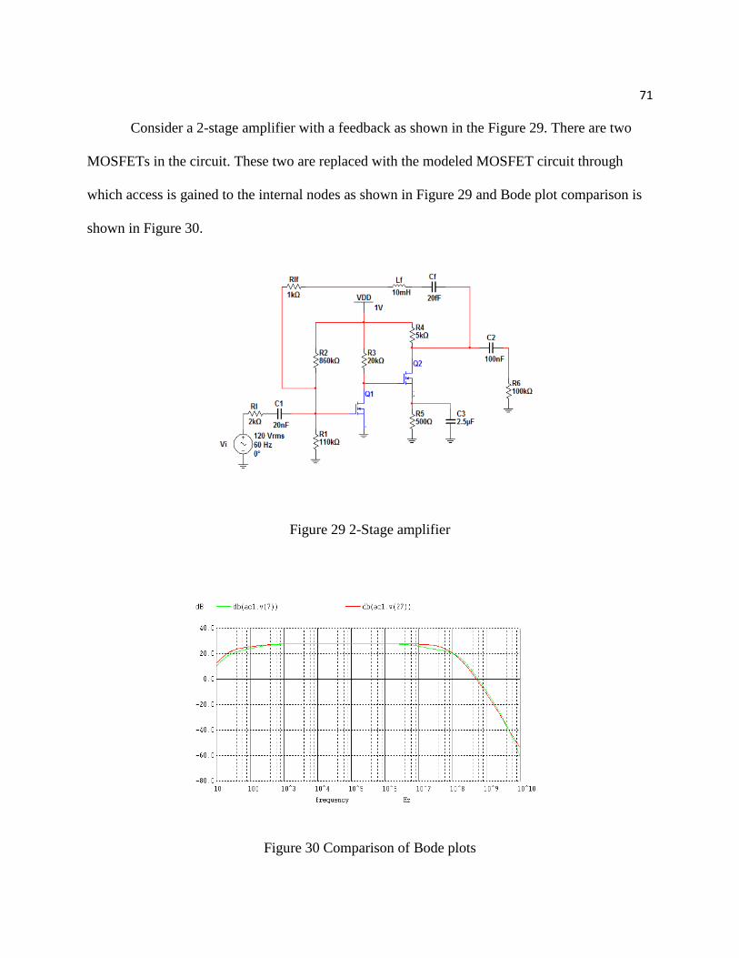
71
Consider a 2-stage amplifier with a feedback as shown in the Figure 29. There are two
MOSFETs in the circuit. These two are replaced with the modeled MOSFET circuit through
which access is gained to the internal nodes as shown in Figure 29 and Bode plot comparison is
shown in Figure 30.
Figure 29 2-Stage amplifier
Figure 30 Comparison of Bode plots

72
An alternative parallel connection of the MOSFETs is shown in Figure 31 and their
comparison results in Figure 32.
Figure 31 Parallel connection of two amplifiers, with feedback compensation subcircuit
Figure 32 Comparison of Bode plots
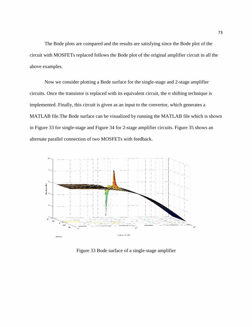
73
The Bode plots are compared and the results are satisfying since the Bode plot of the
circuit with MOSFETs replaced follows the Bode plot of the original amplifier circuit in all the
above examples.
Now we consider plotting a Bode surface for the single-stage and 2-stage amplifier
circuits. Once the transistor is replaced with its equivalent circuit, the σ shifting technique is
implemented. Finally, this circuit is given as an input to the convertor, which generates a
MATLAB file.The Bode surface can be visualized by running the MATLAB file which is shown
in Figure 33 for single-stage and Figure 34 for 2-stage amplifier circuits. Figure 35 shows an
alternate parallel connection of two MOSFETs with feedback.
Figure 33 Bode surface of a single-stage amplifier

74
Figure 34 Bode surface of a 2-stage amplifier
Figure 35 3D Bode surface plot for parallel connection of two amplifiers, with adding a feedback
compensation subcircuit

75
CHAPTER 8
CONCLUSION
The MOSFET modelling has been achieved such that access to internal nodes is obtained
through which design issues can be simplified. These modelled MOSFETs are implemented in a
technique to produce 3D Bode surface which represents poles and zeros. Examples are shown
comparing the results and as well as showing the Bode surface plots in which the modeled
circuits are implemented. The Bode surfaces clearly display the poles and zeros of the transfer
function. One might think that adding large coupling capacitors might cause a time delay. But it
should be noted that the equivalent model generated is for AC analysis only. A different model is
used for the purpose of transient analysis. A new program is developed which allows us to access
WinSpice code through MATLAB. This indirectly adds the feature of obtaining 3D Bode plots
which are not present in SPICE tool. If the two features, having access to the internal circuit of
the transistor and being able to generate 3D surfaces, are added to a tool like P-SPICE, it would
make it a powerful tool to interpret and solve many design issues.

REFERENCES
[1] Hashemian, R., 2015, “S-Plane Bode Plots - Identifying Poles and Zeros in a Circuit Transfer
Function,” Proceedings of the IEEE LASCAS 2015 Conference, Montevideo, Uruguay, February
24 – 27, 2015.
[2] Hashemian, R., 2014, “Extraction of Poles and Zeros of an RC Circuit with Roots on the Real
Axis,” IEEE Trans. Circuits Syst. II, Exp. Briefs, vol. 61, no. 8, pp. 624-628.
[3] Hennig, E., 2002, “Matrix Approximation Techniques for Symbolic Extraction of Poles and
Zeros,” Analog Integrated Circuits and Signal Processing, Vol. 31, Issue 2, pp 81-100.
[4] Hwsupport, n.d., “Complex plane of LTI model visualization,”
http://hwsupport.org/cplane/index.html
[5] HSPICE® Reference Manual: MOSFET Models D-2010.12,
http://www.ele.uri.edu/courses/ele448/HSPICERef