a software approach for combating asymmetries of non-volatile memories
TRANSCRIPT
A Software Approach for Combating Asymmetries ofNon-Volatile Memories
Yong [email protected]
Yiran [email protected]
Alex K. [email protected]
Department of ECE, University of PittsburghPittsburgh, PA, 15261
ABSTRACTThe recent advances in non-volatile memory technologiespromise the delivery of future high performance and lowpower computing systems. While these technologies provideattractive features, they exhibit different degrees of asym-metric read/write behavior, resulting in under utilization ofthe technology benefits in many scenarios. Future systemsshould be aware of this asymmetry to fully utilize thesememory technologies. In this paper, we propose softwaredispatch, a cross-layer approach to distribute data to ap-propriate memory resources based on an application’s dataaccess characteristics. We demonstrate the application ofthe proposed technique through a case study system withhybrid memory caches, on which we achieve over 5% perfor-mance improvement and 9.8% power savings compared tothe state-of-the-art technique.
Categories and Subject DescriptorsB.3 [Hardware]: Memory Structures; D.3.4 [ProgrammingLanguages]: Processors—Compilers, Optimization
General TermsDesign, Experimentation, Performance
KeywordsHybrid Memories, Compilers, Dispatch
1. INTRODUCTIONNon-volatile memory (NVM) technologies are recently un-
dergoing fast development and several of them have alreadybeen successfully applied to many consumer electronic prod-ucts. For example, NAND-flash (Figure 1) based solid-state drives (SSDs) have been widely adopted in embed-ded and mobile devices due to their power efficiency andhigh shock/vibration endurance. Figure 2 displays mag-netic random access memory (MRAM) of which the spin-torque transfer (STT) variety is receiving considerable at-tention [4]. STT-RAM offers various attractive features in-
Permission to make digital or hard copies of all or part of this work forpersonal or classroom use is granted without fee provided that copies arenot made or distributed for profit or commercial advantage and that copiesbear this notice and the full citation on the first page. To copy otherwise, torepublish, to post on servers or to redistribute to lists, requires prior specificpermission and/or a fee.ISLPED’12, July 30–August 1, 2012, Redondo Beach, CA, USA.Copyright 2012 ACM 978-1-4503-1249-3/12/07 ...$10.00.
cluding lower leakage, fast read access and high density. Ithas been demonstrated that incorporating STT-RAM intomobile applications can dramatically reduce standby powerand replacing DRAM with STT-RAM in data centers canreduce power by up to 75% [3]. Other examples of future al-ternative memories include resistive RAM (RRAM) [10] andphase change RAM (PCRAM) [11], as illustrated in Figure 3and Figure 4.
Despite the attractive features of the aforementioned mem-ory technologies, several challenges prevent them from im-mediately and entirely replacing conventional memory/storagesuch as SRAM, DRAM and HDDs (hard disk drives). Onemajor issue is the read/write asymmetries of these NVMs interms of power consumption, access latency and endurance,as summarized in Table 1. For example, NAND flash fea-tures significant asymmetry in its read versus write opera-tion. While it provides flexible and high performance readoperation, its write operation suffers from the limitation oferase-before-write [5], which makes it undesirable for appli-cations with high temporal write reuse patterns. PCRAM,MRAM and RRAM also exhibit different degrees of asym-metric read/write characteristics. Generally, expensive writeoperations of these memories cause performance and powerbottlenecks for write intensive applications.
Table 1: Memories with Asymmetric R/W Charac-teristics
Memory Type NAND Flash MRAM PCRAM RRAMCell Structure 1T 1T1MTJ 1T1R 1T1R
Cell Area 4 ∼ 6F2 6 ∼ 20F2 5 ∼ 12F2 4 ∼ 10F2
Read Latency 20 ∼ 60ns 2 ∼ 10ns 10 ∼ 40ns 5 ∼ 10nsWrite Latency 100 ∼ 1000µs 10 ∼ 20ns 50 ∼ 120ns 10 ∼ 20nsRead Energy low low low lowWrite Energy high high high low
Write Endurance 105 1016 108 108
Prior research efforts have been made to mitigate the over-head incurred by asymmetrically long write penalties forspecific memory technologies. In particular, Lee et al. pro-posed in-page logging (IPL) [6] to alleviate the erase-before-write limitation of NAND flash. IPL reduces the overheadof erase operations by introducing a dedicated log space torecord the data changes. Once the log space is full, a mergeoperation is triggered to write data pages to a clean eraseblock with all of the updates applied. For frequently up-dated data however, this approach leads to intensive mergeoperations, causing significant overhead. Other research at-tempts [16, 9] have been made to mitigate the asymme-try problem by adding conventional memories (CMs) (e.g.,SRAM and DRAM) to different levels of the memory hierar-chy constructed by NVMs such as MRAM and PCRAM. Inthese proposed memory systems, data is distributed by hard-

…
One Cell
Word Line
Source Line
Bit
Lin
e
Data Buffer
Flash Memory
data page
data+log
Up
dat
e in
bu
ffer
Wri
te b
ack
Erase Block
Figure 1: NAND flash
Pinned Layer
Free Layer
MgO
Pinned Layer
Free Layer
MgO
Bit Line
Source Line
Wo
rd L
ine
Figure 2: MRAM
Heater
GST
Top Electrode
Bottom Electrode
Wo
rd L
ine
Bit Line
Figure 3: PCRAM
Top Electrode
Bottom Electrode
Transition Metal Oxide (HOVC) Transition Metal Oxide (LOVC) W
ord
Lin
e
Bit Line
Figure 4: RRAM
ware between NVM and CM to achieve a balanced read/writeperformance. However, these approaches are typically de-signed for specific memory levels (e.g., cache and main mem-ory) and do not effectively leverage applications’ data accesscharacteristics.
We study the read/write asymmetry as a generic prob-lem of various NVMs used in different levels of the memoryhierarchy including scratchpad memories, caches and mainmemory. In this paper, we propose SPD (software dispatch),a cross-layer solution including the compiler and OS (oper-ating system) that captures applications’ data access char-acteristics to guide the hardware and distribute data amonghybrid memories1 for optimized performance and power con-sumption. We evaluate our approach on a case study hybridmemory system and demonstrate that software dispatch en-sures that 88.5% of writes are handled in CM, which onlycomprises 3% of the total cache capacity. Through softwaredispatch we achieve over 5% performance improvement andnearly 10% power saving compared to the state-of-the-artruntime technique.
2. UTILIZING HYBRID MEMORIESThe availability of various memory technologies brings the
potential for building a rich set of hybrid memory systemsthat trade off among performance, power and density. Dueto the relatively high penalty of write accesses, systems uti-lizing NVMs typically need to incorporate certain amountof CM for data that is write intensive. The methodologyfor including CM to form hybrid memory systems could bedifferent, depending on scenarios.
One typical organization of hybrid memories is using CMas a buffer for NVM. For example, the entire secondary stor-age can be constructed using one type of the NVMs witha small block of CM serving as a write buffer. The SSDsdiscussed in Section 1 (Figure 1) is one type of such hy-brid memory systems. Another example is using PCRAMas main memory with a DRAM buffer [11].
Hybrid memories can be also utilized for building scal-able, high density and low power on-chip caches with writethrough policy [16, 14], which is supported by various com-mercial CPU products including Intel Pentium, Sandy/IvyBridge, UltraSparc, etc. For future CMPs with large numberof cores, write-through caches are becoming more attractiveas they greatly simplify the cache coherence protocol, whichcould be extremely complex with numerous transient states.Unfortunately, a write-through policy defeats the CM bufferfor NVM, exposing write intensive behavior to lower levels inthe memory hierarchy that are candidates to utilize NVMssuch as last level cache. Thus, a scalable and efficient cachearchitecture can be built by employing hybrid memories in
1Different NVMs can comprise hybrid memories. In thispaper we restrict the term hybrid memories to the systemswhere both NVMs and conventional memories are used.
which each cache set contains a mixture of NVM blocks andCM blocks, as depicted in Figure 5(a). Since the NVM istypically write-hostile and the CM is write-friendly, it is de-sirable that write intensive data be dynamically migrated orswapped from the NVM to the CM. A common hardwareapproach is to keep track of a short history of write accessesusing a counter and migrate/swap a data block from thewrite-hostile memory to the write-friendly memory if thecounter indicates the data block is write intensive. This ap-proach however, is easily misled by unpredictable runtimedata access behavior. Significant mispredictions can incuran expensive penalty of serving accesses in the wrong typeof memory (e.g., write frequent accesses occurring in NVM)as well as large migration/swap overhead. In contrast, asoftware mechanism has the advantages of taking actionspreemptively to hide the migration/swap latency from thecritical path and detecting data access patterns more accu-rately compared to simple run-time approaches.
CM (Write-
Friendly)
NVM
(Write- Hostile) Decoder
Counter Migration/Swap
Control
Write Req.
Software Guide
(a)
Cache One Cache Set
NVM (Write- Hostile)
CM (Write-
Friendly) W
rite
R
eq.
Dec
od
er
Mem
ory
Map
pin
g/
Allo
cati
on
Co
ntr
ol
So
ftw
are
Gu
ide
(b)
Main Memory
HA
R
LAR
A
dd
ress
D
ecre
asin
g
Figure 5: Utilizing hybrid memories at different lev-els (a): hybrid memories for caches (b): hybridmemories for main memory
Building main memory using NVM and CM has also beenstudied [9]. One typical organization for hybrid main mem-ory separates NVM and CM into independently addressedmemory regions (e.g., high address region (HAR) versus lowaddress region (LAR)), as shown in Figure 5(b). Data witha certain read/write characteristic is allocated or mappedonto a specific address region so that it can be served by anappropriate type of memory. For example, the OS can mapa read-only virtual page to a physical page served by thewrite-hostile NVM to leverage its non-volatility, low leakageand large capacity benefits without bringing negative perfor-mance or power impact. To achieve this, the OS needs to beaware of the physical address regions comprised by hybridmemories as well as the application’s data access character-istics at the page granularity.
As can be seen from the above discussions, hybrid memorysystems can be effectively assisted and optimized by softwaremechanisms, which will be detailed in the next section.
3. SOFTWARE DISPATCHIn this section we discuss the proposed software dispatch
technique that leverages an application’s data access char-acteristics to optimize the utilization of hybrid memory sys-tems introduced in the previous section.
3.1 Compiler Dispatch for Migration/SwapIn hybrid NVM-CM systems with migration or swap sup-
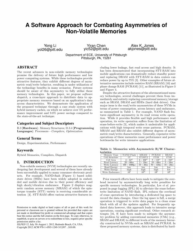
port (e.g., Figure 5(a)), the migration or swap decisionsshould be made based on various factors including the appli-cation’s write access patterns and the migration/swap over-head. In order to minimize the overhead, it is importantthat only the actively write intensive data is migrated orswapped from the NVM to the CM. To achieve this goal, wepropose compiler-based dispatch, which identifies the writereuse patterns of heap data objects including arrays andlinked structures and inserts instructions to guide the hard-ware to perform the migration/swap dynamically.
3.1.1 Write Reuse Identification for ArraysTo make migration/swap decisions for a memory block
containing continuous bytes, we detect the temporal andspatial write reuses from array accesses in the source pro-gram.
Consider Figure 6 as an example. Given the array ac-cesses A[i+2][ j] and B[2][i][2∗ i+1] in the nested loop shownin Figure 6(a), we first convert the subscript functions tothe matrix expressions, as illustrated in Figure 6(b). Thearray access now can be represented as C ∗ k +O, where C isthe coefficient matrix, k is the index vector and O denotesthe offset vector. Determining whether the array access hastemporal write reuse now is equivalent to deriving the con-dition under which the equation C ∗ k′ + O = C ∗ k′′ + O hassolutions [15] (k′ and k′′ represent two different index vec-tors in the iteration space). The necessary and sufficientcondition under which the above equation has solutions isthat C is not full ranked. In our example, the coefficientmatrix of A[i + 2][ j] has a rank of 2, indicating no temporalreuse. B[2][i][2∗ i+1] has temporal reuse since the rank of itscoefficient matrix is 1, which is smaller than its dimension.
Coefficient Matrix For A[i+2][j]
Coefficient Matrix For B[2][i][2*i+1]
1 0 0 1
0 0 1 0 2 0
i j
i j
*
*
+
+
2 0
2 0 1
Truncated Matrix Offset Matrix for(i=0;i<N;i++) for(j=0;j<M;j++) {
A[i+2][j] = 0; B[2][i][2*i+1]+=1; }
(a) (b)
Figure 6: Array accesses and the corresponding ma-trix representations (a): array accesses (b): matrixrepresentation
An array write access exhibits spatial write reuse whenthe innermost enclosing loop index varies only the last coor-dinate of that array. To discover spatial write reuse, we usea truncated coefficient matrix by dropping the last row ofthe original coefficient matrix, as illustrated in Figure 6(b).If the rightmost column in the truncated coefficient ma-trix (the coefficients that correspond to the innermost loopindex) is a null vector and the rightmost element in thedropped row is nonzero, it is assured that the innermostloop only varies the last coordinate of the corresponding ar-ray.
In the above example, A[i + 2][ j] exhibits spatial reuse
since the rightmost column in the truncated matrix (the co-efficient corresponding to the innermost loop index j) is anull vector and the rightmost element in the dropped rowis nonzero. Using the same rule we can determine thatB[2][i][2 ∗ i + 1] does not have spatial reuse since the in-nermost loop index j does not vary in the last coordinate ofarray B.
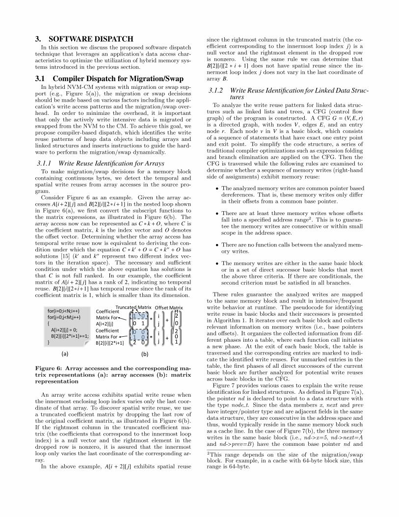
3.1.2 Write Reuse Identification for Linked Data Struc-tures
To analyze the write reuse pattern for linked data struc-tures such as linked lists and trees, a CFG (control flowgraph) of the program is constructed. A CFG G = (V, E, r)is a directed graph, with nodes V, edges E, and an entrynode r. Each node v in V is a basic block, which consistsof a sequence of statements that have exact one entry pointand exit point. To simplify the code structure, a series oftraditional compiler optimizations such as expression foldingand branch elimination are applied on the CFG. Then theCFG is traversed while the following rules are examined todetermine whether a sequence of memory writes (right-handside of assignments) exhibit memory reuse:
• The analyzed memory writes are common pointer baseddereferences. That is, these memory writes only differin their offsets from a common base pointer.
• There are at least three memory writes whose offsetsfall into a specified address range2. This is to guaran-tee the memory writes are consecutive or within smallscope in the address space.
• There are no function calls between the analyzed mem-ory writes.
• The memory writes are either in the same basic blockor in a set of direct successor basic blocks that meetthe above three criteria. If there are conditionals, thesecond criterion must be satisfied in all branches.
These rules guarantee the analyzed writes are mappedto the same memory block and result in intensive/frequentwrite behavior at runtime. The pseudocode for identifyingwrite reuse in basic blocks and their successors is presentedin Algorithm 1. It iterates over each basic block and collectsrelevant information on memory writes (i.e., base pointersand offsets). It organizes the collected information from dif-ferent phases into a table, where each function call initiatesa new phase. At the exit of each basic block, the table istraversed and the corresponding entries are marked to indi-cate the identified write reuses. For unmarked entries in thetable, the first phases of all direct successors of the currentbasic block are further analyzed for potential write reusesacross basic blocks in the CFG.
Figure 7 provides various cases to explain the write reuseidentification for linked structures. As defined in Figure 7(a),the pointer nd is declared to point to a data structure withthe type node t. Since the data members x, next and prevhave integer/pointer type and are adjacent fields in the samedata structure, they are consecutive in the address space andthus, would typically reside in the same memory block suchas a cache line. In the case of Figure 7(b), the three memorywrites in the same basic block (i.e., nd->x=5, nd->next=Aand nd->prev=B) have the common base pointer nd and
2This range depends on the size of the migration/swapblock. For example, in a cache with 64-byte block size, thisrange is 64-byte.

Algorithm 1: Pseudocode for write reuse identificationof linked data structures in CFG G(V, E, r)
for each basic block bi ∈ V docreate table H;phase = 0;for each statement s j ∈ bi do
if s j is function call thenphase + +;
elseget the base pointer bp of LHS (s j);get the offset o of LHS (s j);if ∃ entry Y ∈ H such that bp = Y.bp &&phase = Y.phase then
append o to Y;else
push o, phase and bp into H;end if
end ifend fortraverse H and mark entries with more than 2 offsetsin a single phase that are within the specified range;for each unmarked entry Y ′ ∈ H do
for each block b j ∈⋃
S UCC(bi) dosearch Y ′.bp in the first phase in b j and computethe total number of offsets n that are within thespecified range;if n < 3 then
continue to process next unmarked entry;end if
end formark entry Y ′;
end forend for
there is no interleaved function calls. Thus, Figure 7(b) ex-hibits write reuse. The program in Figure 7(c) also has writereuse since both successors of the basic block nd->x=5 leadto write reuse. Figure 7(d) does not exhibit write reuse dueto the presence of the function call foo(). In Figure 7(e), oneof the direct successors nd->next=A only has one commonpointer based memory write and thus, will not be markedas having write reuse.
3.1.3 Pre-dispatch InstrumentationOnce the write reuse has been determined, the compiler
inserts a pre-dispatch instruction into the code prior to thememory access to notify the CPU to perform the migra-tion or swap operation. The pre-dispatch instruction can beimplemented using the extra bits in the instruction opcodeof a particular ISA. For example, in SPARC, the prefetchinstruction provides dedicated field fcn to implement vari-ants of prefetch instruction. The fcn value from 16 to 31 iscurrently reserved and can be used to implement our pre-dispatch instruction. In the ARM architecture, there aresimilar reserved bits that can be used to implement the mi-gration/swap operation.
3.2 OS/Allocator DispatchWhen data cannot be migrated/swapped on demand due
to memory organization limitations (e.g., system illustratedin Figure 5(b)), the OS or the memory allocator (e.g., mal-loc(), new) can be used to dispatch3 the data at the memory
3In this scenario, dispatch refers to the software procedurethat maps or allocates data to a particular type of memory.
nd->x = 5; nd->next = A; nd->prev = B;
typedef struct node { … int x; struct node *next; struct node *prev; … } node_t; node_t *nd;
nd->x = 5;
nd->next = A; nd->prev = B;
nd->next = B; nd->prev= A;
nd->x = 5;
nd->prev = B;
nd->next = B; nd->prev= A;
nd->x = 5; foo();
nd->next = A; nd->prev = B;
nd->next = A;
(a)
(b)
(d)
(c)
(e)
…
Figure 7: Code and control flow graph examples forwrite reuse identification. (a): type definition code(b): write reuse in the same basic block (c): writereuse across one basic block and all its successors(d): write reuse broken by function call (e): writereuse broken by one successor
allocation time. This requires a load-time understanding ofaccess characteristics of the memory blocks so that they canbe allocated onto appropriate types of memories that bestserve them. A heuristic observation is that pages in dif-ferent virtual segments (e.g., text/code, heap, stack) exhibitdistinct access patterns. The pages in the code segment con-tain only instructions and are predominantly read-only. Thepages in the stack typically exhibit a high write reuse patterndue to the way the stack operates. Thus, the OS can dis-patch all the instruction pages to the write-hostile memoryand stack pages to the write-friendly memory through itsvirtual-to-physical memory mapping process. In contrast,heap pages consist of dynamically allocated objects exhibit-ing diverse and application-dependent data access patterns.To analyze write access patterns for heap objects, the com-piler techniques presented in Section 3.1 can be adopted.The analyzed results for a particular heap object can bepropagated back to the memory allocation point (e.g., thecall site of malloc()) using data flow analysis [7] to helpmaking the dispatch decision.
4. CASE STUDY AND EVALUATIONTo demonstrate the application and impact of software
dispatch on hybrid memory systems, we design and evalu-ate a case study system with hybrid SRAM-STT caches onwhich we applied the proposed techniques.
Table 2: SRAM and STT-RAM Parameters (45nm)
Size 128K SRAM 512K STT-RAMArea 1.339mm2 1.362mm2
Read Latency 1.778ns 1.823nsWrite Latency 1.868ns 8.725nsRead Energy 0.574nJ 0.550nJWrite Energy 0.643nJ 3.243nJLeakage Power 0.185W 0.013W
4.1 Case Study and Experimental SettingsOur experimental system consists of 16 cores laid out
as a 4 × 4 mesh. The L1 cache is purely SRAM whilethe L2 utilizes both SRAM and STT-RAM. The SRAMand STT-RAM layers are stacked using 3D through sili-con vias (TSVs) [12] technology, as illustrated in Figure 8.As a software-guided data distribution scheme, we comparewith the mechanism that migrates data from STT-RAM toSRAM upon two successive writes (MSW), a relevant hard-ware approach presented in [14]. We do not compare with

other techniques proposed in [14] since they are either or-thogonal to data distribution and thus can equally benefita variety of systems including ours or applicable in differentscenarios from ours.
We use HSPICE simulation and modified CACTI [13] tomodel the latency, power and area of the simulated caches.We observe that a 128K SRAM bank takes up comparablechip area to a 512K STT-RAM bank, as shown in Table 2.The detailed architectural parameters simulated are shownin Table 3.
Switch/ Routing
Logic
31 Lines
Core L1 Dir
1 Line
One Associativity
STT-RAM Bank
SRA
M L2
STT-RAM Buffer
TSB
Figure 8: 3-D Architecture with hybrid SRAM-STTcaches.
Table 3: Architecture configurations
SRAM L2 STT-RAM L2Processor 16 SPARC cores, 2G Hz, 4W/core
Operating System 64-bit Solaris 10
L1 Cache16KB/core, 4-way associative,64B block size, 1-cycle hit la-tency, write-through
L1 Coherence MESI protocol, in cache directoryL2 Cache Size 128KB/bank 512KB/bankL2 Block Size 64B 64B
L2 Associativity 32 32L2 Read Latency 4 cycles 4 cyclesL2 Write Latency 4 cycles 18 cycles
L2 Energy refer to Table 2
Network4×4 Mesh, packet switching, 3cycles per hop
Main Memory 4GB, 150-cycle latency
In our experiment we apply the proposed technique on awrite-back L2 with write-through L1 (see Section 2). Ourapproach also applies to L1 caches (either write-back orwrite-through) and scratchpad memory. We utilize multi-threaded workloads from the SPLASH-2 [1] and PARSEC [2]benchmark suites and Wind River Simics [8] as our simula-tion environment.
4.2 Performance and Power EvaluationFigure 9 reports the ratio of write operations served by
SRAM versus STT-RAM for MSW and software dispatch(SPD). In MSW, two successive writes on the same datablock result in a migration and the subsequent writes onthat block will be served by SRAM. This allows the SRAM,which comprises just over 3% of the cache capacity to serve39.6% of the writes. However, MSW does not perform anaccurate prediction for write reuse when applications exhibitcertain interleaved read/write access patterns. In contrast,SPD dispatches more effectively and results in an average of88.5% of all the write requests being handled in SRAM.
Another important metric in our evaluation is the numberof writes on SRAM per dispatch operation. The larger thenumber, the lower the dispatching overhead relative to thegain. Figure 10 presents the number of SRAM writes per
FLUIDANIMATECHOLESKY RAYTRACE WATER-SPATIAL
0.96875 0.96875 0.96875 0.96875 0.96875
0.03125 0.03125 0.03125 0.03125 0.03125
0.667574 0.678857 0.398546 0.4703899 0.603771
0.332426 0.321143 0.601454 0.5296101 0.396229
0.03986 0.286924 0.03046 0.0184389 0.114789
0.96014 0.713076 0.96954 0.9815611 0.885211
0%
20%
40%
60%
80%
100%
Rat
io o
f W
rite
s In
curr
ed
on
SR
AM
vs
STT
-RA
M
SRAM Writes (MSW)STT-RAM Writes (MSW)
SRAM Writes (SPD)STT-RAM Writes (SPD)
Figure 9: Ratio of writes on SRAM vs STT-RAMfor MSW and SPD
dispatch for MSW and SPD. SPD has a much larger numberof writes on SRAM per dispatch/migration. On average, 32writes are served by SRAM per one migration operation inSPD while there are only 8 writes occur in SRAM per onemigration in MSW.
0
15
30
45
60
75
90
Nu
mb
er o
f SR
AM
Wri
tes
SRAM Writes/Migration (MSW) SRAM Writes/Migration (SPD)
Figure 10: Number of SRAM writes per dispatch(migration)
The off-chip miss rate shown in Figure 11 demonstratesthe advantage of reduced off-chip miss rate achieved by em-ploying STT-RAM for on-chip storage. With 4 times morecapacity than SRAM-only L2 caches, MSW and SPD reducethe off-chip misses by 38.9% and 40.0%, respectively. The re-duction in expensive off-chip misses results in an average of5% faster memory accesses for SPD, as shown in Figure 12.MSW exhibits a negligible improvement in memory accessdelay despite the reduction in off-chip misses as this benefitis offset by the large number of writes on STT-RAM (seeFigure 9).
0%20%40%60%80%
100%
No
rmal
ized
Mis
s R
ate
SRAM MSW SPD
Figure 11: Normalized off-chip miss rate
Figure 13 shows the static and dynamic power breakdownnormalized to the total power consumption of the SRAMcache. Due to the leakage problem inherited by CMOSdevices, the SRAM-only cache consumes a non-negligibleamount of static power while MSW and SPD dramaticallyreduce it. However, MSW consumes an average of 18.4%more dynamic power than the SRAM-only design due tothe high energy overhead incurred by writes on STT-RAM.In contrast, the dynamic power consumed by SPD is closeto that consumed by the SRAM-only cache since most ofthe writes in SPD have been dispatched efficiently onto its

0.8
0.9
1
1.1
1.2
No
rmal
ized
Mem
ory
Del
ay SRAM MSW SPD
Figure 12: Normalized memory access delay
SRAM fraction. MSW results in an 0.3% overall higherpower consumption than SRAM-only in spite of its 86.6%static power reduction. SPD has a similar static power sav-ings of 86.8% as well as a total power savings of 9.8%.
Normalized to SRAM Total Power
OCEAN BLACKSCHOLESBARNES LU STREAMCLUSTERFFT SWAPTIONS
SRAM Static Power0.236362 0.103014 0.114322 0.105626 0.2748142 0.163556 0.171881
SRAM Dynamic Power0.763638 0.896986 0.885678 0.894374 0.7251858 0.836444 0.828119
SRAM Total Power 1 1 1 1 1 1 1
MSW Static Power0.026731 0.016797 0.016232 0.020616 0.0328027 0.018687 0.023397
MSW Dynamic Power0.905468 1.444958 1.060511 1.124662 0.6037346 0.906224 0.942394
MSW Total Power0.932199 1.461755 1.076743 1.145279 0.6365372 0.924911 0.965791
SPD Static Power 0.026517 0.016491 0.015199 0.021306 0.0330237 0.017752 0.023233
SPD Dynamic Power0.817795 0.920065 0.886957 0.887443 0.7490372 0.881813 0.892867
SPD Total Power 0.844311 0.936555 0.902156 0.908749 0.782061 0.899565 0.9161
0
0.2
0.4
0.6
0.8
1
1.2
Stat
ic, D
ynam
ic a
nd
To
tal P
ow
er
(No
rmai
lized
to
SR
AM
To
tal P
ow
er)
SRAM Dynamic PowerSRAM Static Power
MSW Dynamic PowerMSW Static Power
SPD Dynamic PowerSPD Static Power
1.44
Figure 13: Normalized power consumption
5. CONCLUSIONIn this paper, we presented software dispatch, an approach
to detect write reuse patterns within the application and usethis information to guide the hardware and distribute dataaccesses to appropriate memory resources in hybrid memorysystems. Our evaluation through a case study system withhybrid memory caches demonstrates using software dispatchthe number of writes serviced by conventional memory isincreased by 81%, memory access performance is improvedby 5% and memory power consumption is reduced by 10%over the state-of-the-art runtime system.
6. ACKNOWLEDGEMENTThis work is supported, in part, by NSF award CCF-
1064976.
7. REFERENCES[1] J. M. Arnold, D. A. Buell, and E. G. Davis. Splash 2.
In SPAA ’92: Proceedings of the fourth annual ACMsymposium on Parallel algorithms and architectures,pages 316–322, New York, NY, USA, 1992. ACM.
[2] C. Bienia, S. Kumar, J. P. Singh, and K. Li. Theparsec benchmark suite: Characterization andarchitectural implications. Technical ReportTR-811-08, Princeton University, January 2008.
[3] A. Driskill-Smith. Latest advances and futureprospects of stt-ram. Non-Volatile MemoriesWorkshop, 2010.
[4] M. Hosomi, H. Yamagishi, T. Yamamoto, and K. B.et al. A novel nonvolatile memory with spin torquetransfer magnetization switching: Spin-ram. IEDMTechnical Digest, 2(25):459–462, 2005.
[5] J.-U. Kang, H. Jo, J.-S. Kim, and J. Lee. Asuperblock-based flash translation layer for nand flashmemory. In Proceedings of the 6th ACM & IEEEInternational conference on Embedded software,EMSOFT ’06, pages 161–170, New York, NY, USA,2006. ACM.
[6] S.-W. Lee and B. Moon. Design of flash-based dbms:an in-page logging approach. In Proceedings of the2007 ACM SIGMOD international conference onManagement of data, SIGMOD ’07, pages 55–66, NewYork, NY, USA, 2007. ACM.
[7] Y. Li, A. Abousamra, R. Melhem, and A. K. Jones.Compiler-assisted data distribution for chipmultiprocessors. In PACT ’10: Proceedings of the 19thinternational conference on Parallel architectures andcompilation techniques, pages 501–512, New York, NY,USA, 2010. ACM.
[8] P. S. Magnusson, M. Christensson, J. Eskilson,D. Forsgren, G. Hallberg, J. Hogberg, F. Larsson,A. Moestedt, and B. Werner. Simics: A full systemsimulation platform. IEEE Computer, 35(2):50–58,February 2002.
[9] J. C. Mogul, E. Argollo, M. Shah, and P. Faraboschi.Operating system support for nvm+dram hybrid mainmemory. In Proceedings of the 12th conference on Hottopics in operating systems, HotOS’09, pages 14–14,Berkeley, CA, USA, 2009. USENIX Association.
[10] C. Muller, D. Deleruyelle, O. Ginez, J.-M. Portal, andM. Bocquet. Design challenges for prototypical andemerging memory concepts relying on resistanceswitching. In Custom Integrated Circuits Conference(CICC), 2011 IEEE, pages 1–7, September 2011.
[11] M. Qureshi, M. Franceschini, and L. Lastras-Montano.Improving read performance of phase changememories via write cancellation and write pausing. InHigh Performance Computer Architecture (HPCA),2010 IEEE 16th International Symposium on, pages 1–11, jan. 2010.
[12] K. Sakuma, P. S. Andry, C. K. Tsang, S. L. Wright,B. Dang, C. S. Patel, B. C. Webb, J. Maria, E. J.Sprogis, S. K. Kang, R. J. Polastre, R. R. Horton, andJ. U. Knickerbocker. 3d chip-stacking technology withthrough-silicon vias and low-volume lead-freeinterconnections. IBM J. Res. Dev., 52:611–622,November 2008.
[13] P. Shivakumar and N. P. Jouppi. Cacti 3.0: Anintegrated cache timing, power, and area model.Technical report, hp, August 2001.
[14] G. Sun, X. Dong, Y. Xie, J. Li, and Y. Chen. A novelarchitecture of the 3d stacked mram l2 cache for cmps.In Proceedings of the High Performance ComputerArchitecture, pages 239–249, 2009.
[15] M. E. Wolf. Improving locality and parallelism innested loops. PhD thesis, Stanford, CA, USA, 1992.UMI Order No. GAX93-02340.
[16] X. Wu, J. Li, L. Zhang, E. Speight, R. Rajamony, andY. Xie. Hybrid cache architecture with disparatememory technologies. In Proceedings of the 36thannual international symposium on Computerarchitecture, ISCA ’09, pages 34–45, New York, NY,USA, 2009. ACM.