a quick start to tinalab ii fpga development kit
TRANSCRIPT

A Quick Start To
TINALab II FPGA Development Kit
2009 www.designsoftware.com

2

3
OVERVIEW The TINALab Spartan-II FPGA Development Kit provides an easy-to-use, low-cost evaluation platform for developing designs and applications based on the Xilinx Spartan-II FPGA family. The kit can be physically connected to the User Port of TINALab II or can be used stand alone with an external power supply, a Xilinx JTAG programming cable and the free Xilinx ISE WebPACK software. The board is mounted with a 144-pin TQFP (thin quad flat-pack) Xilinx Spartan-II device (up to 100,000-gate XC2S100-5TQ144) gives users high performance, abundant logic resources, and a rich feature set. Features include block RAM, distributed RAM, 16 selectable I/O standards, and four DLLs. If you use TINALab Spartan-II together with TINA circuit simulation software and TINALab II High Speed Multifunction PC Instrument there is possible to develop VHDL code with simulation capabilities and after implementing, you can download your design and measure back the signals with the help of TINALab II Digital Signal Generator and Logic Analyzer. TINA provides code developing, simulation and measurement control with TINALab II, which does power supplies and signal link. Forty-two user I/O signals from the FPGA are connected to user headers. The board includes the XCF01S ISP configuration Xilinx Platform Flash, a JTAG header, and a configuration mode connector, an on-board socketed clock oscillator, VGA, PS2, RS-232 serial port, four seven-segment LEDs, user LEDs, slide switches, and push buttons. HIGHLIGHTS OF TINALAB SPARTAN-II FPGA DEVELOPMENT BOARD
• XC2S100-5TQ144 FPGA, system performance supported up to 200MHz operation • Xilinx XCF01S 1Mbit Platform Flash Configuration PROM for non-volatile designs • JTAG-programmable • On-board 1A voltage regulators (2.5V core, 3.3V I/O) • JTAG programming port • 50MHz SMD crystal oscillator • Socket for a second oscillator • 92 user I/O’s routed to on-board devices and three expansion connectors • 9-pin RS-232 Serial Port • PS/2-style mouse/keyboard port • 6-bit, 64-colour VGA display port • Ladder R/2R 4-bit DAC • 8 individual LEDs • 4-digit seven-segment display • 4 momentary-contact pushbuttons • 8 slide switches

4
TINALAB SPARTAN-II DEVELOPMENT KIT CONNECTED TO TINALAB II
TINA > Schematic and VHDL based circuit simulator > Measurement control > Virtual instruments
USB
TINALab II > High speed multifunctional PC instrument > Digital Signal Generator and Logic Analyzer
Xilinx ISE WebPACK > Implementing FPGA > Create download file
Power supply JTAG interface
Digital out Digital in
TINALab Spartan-II FPGA Kit

5
VHDL DESIGN FLOW
RTL level Simulation
Design Entry (schematic or VHDL)
Place & Route
Synthesis
Configuration Download Virtual Instruments
Digital Signal Generator Logic Analyzer
TINALab Spartan-II FPGA Card
Results in TINA Diagram Window

6
ONBOARD HEADERS AND CONNECTORS J1 TINALab II Logic Analyzer
Note, if you do not use the Logic Analyzer then J1 can be used as generic User I/O.
J2 TINALab II Digital Signal Generator Connector Note, if you do not use the Digital Signal Generator then J2 can be used as generic User I/O.
J3 User I/O Note, - that if you apply Slave Parallel configuration mode then J3 is the byte-wide data and miscellaneous control during the configuration.
J4 TINALab II User Port Connection J5 9-pin RS232 serial port J6, J7 N.C. J8 External power supply connector (+5V) J9 Multilink connector (JTAG, configuration link, JTAG chain broker) J10 PS2 port J11 VGA port JP1 Power supply and configuration jumper
Close pin 1-2 to be powered by TINALab II, 2-3 by external +5V. JP2 FPGA configuration jumpers JP3 R/2R Ladder DAC output JP4 PROM interface jumper JP5 PS2 port supply voltage jumper
TINALab IIUser Port
TINALab IIDigital Signal Generator
TINALab II Logic Analyzer
RS232
VGA
+5V
PS2
On-board Regulators
Multilink connector
ISP Flash2nd oscillator socket
Interface selector jumper
Spartan FPGA
FPGA program memory clear switch Userswitches
User pushbuttons
DONE LED
PS2 power supply

7
CONFIGURATION SUPPORT Configuration is the process by which the bitstream of a design, as generated by the Xilinx development software, is loaded into the internal configuration memory of the FPGA. The TINALAB Spartan-II Development Board supports several different FPGA configuration modes, which are described below. When you use TINALab FPGA board with TINALab II the board is powered, configured, driven and measured by the instrument. Without TINALab II, you need a +5V external power supply and configuration hardware (see http://xilinx.com/products/design_resources/config_sol/index.htm). At the end of the configuration flow FPGA drives DONE high and board DONE LED (D2) goes up. TINALAB II USER PORT When you use TINALab FPGA board with TINA and TINALab II, a 2x7 ribbon cable provides connection from the instrument to the board J4 block header connector. TINALAb II supplies the board with power and configures the FPGA in slave serial mode. To set up, follow these steps:
1. Remove connections from J9 header pin 2, 6, 8, 10 and J3. 2. Remove external power supply plug from J8. 3. Open all the jumpers of JP2 (Slave Serial mode) 4. Close JP4 pin 2 to 3 and JP1 pin 1 to 2 5. Switch off TINALab II 6. Connect TINALab II User Port to that of TINALab FPGA card (J4) with the 14-wire wide
cable 7. Connect TINALab II Digital Outputs to the TINALab II Digital Signal Generator
Connector (J2) 8. Connect TINALab II Digital Inputs to the TINALab II Logic Analyzer Connector (J1) 9. Switch on TINALab II
USING THE TINALAB FPGA BOARD WITHOUT TINALAB II When you use TINALab FPGA board without TINALab II, FPGA can be configured using one of the four Spartan-II configuration modes: slave/master serial, slave parallel and Boundary Scan (JTAG) mode. The Configuration mode pins (JP2: M2, M1, M0) select among these configuration modes with the option in each case of having the IOB pins either pulled up or left floating prior to configuration. Configuration mode Preconfig
pull-ups M0 M1 M2
Master Serial No 0 0 0 Master Serial Yes 0 0 1 Slave Parallel Yes 0 1 0 Slave Parallel No 0 1 1 Boundary Scan Yes 1 0 0 Boundary Scan No 1 0 1 Slave Serial Yes 1 1 0 Slave Serial No 1 1 1

8
In any case, remove TINALab II User Port Connection if it has been used before and close JP1 pin 2 to 3 for the powering. The other steps are depending on the configuration method found in detail the later description. In every mode the last step is to connect the external power supply. JTAG CHAIN Multilink connector provides connection to the board JTAG chain, as shown below. Opening the J9 pin 12 and 14 can break the JTAG chain. Using flying JTAG cable leads to intercept either the ISP FLASH TDO or the FPGA TDI. Set JP2 configuration mode pins in Boundary scan mode. SLAVE SERIAL In serial slave mode, the FPGA is configured by external configuration hardware, e.g.: Xilinx Parallel Cable IV connected Multilink connector (J9) as shown below. Open all JP2 jumpers and close JP4 pin 2 to 3.
MASTER SERIAL In Master Serial mode, the CCLK output of the FPGA drives the Xilinx PROM, which feeds a serial stream of configuration data to the FPGA’s DIN input. According to the mode set JP2 and close JP4 pin 1 to 2.
1 3 5 7 11 12 13 14
TMSTDI TDOTCK
TMS TDI
TDO TCK
GND
+3.3V
TMSTDI TDO TCK
ISP FLASH
FPGA
DIN DONE CCLK
PROG INIT
+3.3V GND

9
SLAVE PARALLEL The Slave Parallel mode is the fastest configuration option. Byte-wide data is written into the FPGA through the Multilink and J3 connector. Set JP2 and close JP4 pin 2 to 3. USER RESOURCES CLOCK SOURCES A 50 MHz SMD oscillator (mounted on the bottom side of the PCB) provides the primary clock source for the TINALab FPGA Board. A second 3.3V oscillator can be plugged into an on-board 14-pin socket. The socket accepts either full- or half-can oscillators. With a 50 MHz clock source, the user can take advantage of the Spartan-II FPGAs internal clock management block, the DLL. The Spartan-II DLL can deskew an incoming clock across the FPGA, providing zero delay with respect to the user source clock. The DLL can provide multiple phases of the source clock. The DLL can also act as a clock doubler, or it can divide the user source clock by up to 16. NET "CLK" LOC = "P88"; On-board SMD oscillator (Y2) NET "GCK3" LOC = "P15"; Socketed 3.3V oscillator (Y1) PUSH BUTTONS The Spartan-II development board design provides four push button switch inputs to the Spartan-II FPGA. Each push button switch can be used to generate an active low signal. When the switch is pressed, FPGA input connected to ground (logic low), when released, internal Spartan-II pull-ups are required to generate logic high. Any push button can be designated to be a RESET signal into the FPGA. Note, there is a fifth button labeled PROG (SW1), which is used to initiate a configuration sequence when pushed. It is not intended to be a general-purpose input. NET "push<0>" LOC = "P139"; Push button 0 input NET "push<1>" LOC = "P138"; Push button 1 input NET "push<2>" LOC = "P137"; Push button 2 input NET "push<3>" LOC = "P136"; Push button 3 input NET "push<0>" PULLUP; Internal pull-up resistor NET "push<1>" PULLUP; Internal pull-up resistor NET "push<2>" PULLUP; Internal pull-up resistor NET "push<3>" PULLUP; Internal pull-up resistor

10
SLIDE SWITCHES The TINALab FPGA development board provides eight slide switch inputs. These switches can be statically set to a low or high logic level. When the switch is disconnected from ground (logic low), internal Spartan-II pull-ups are required to generate logic high. NET "switch<0>" LOC = "P11"; Slide switch 0 input NET "switch<1>" LOC = "P12"; Slide switch 1 input NET "switch<2>" LOC = "P13"; Slide switch 2 input NET "switch<3>" LOC = "P19"; Slide switch 3 input NET "switch<4>" LOC = "P23"; Slide switch 4 input NET "switch<5>" LOC = "P22"; Slide switch 5 input NET "switch<6>" LOC = "P21"; Slide switch 6 input NET "switch<7>" LOC = "P20"; Slide switch 7 input NET "switch<0>" PULLUP; Internal pull-up resistor NET "switch<1>" PULLUP; Internal pull-up resistor NET "switch<2>" PULLUP; Internal pull-up resistor NET "switch<3>" PULLUP; Internal pull-up resistor NET "switch<4>" PULLUP; Internal pull-up resistor NET "switch<5>" PULLUP; Internal pull-up resistor NET "switch<6>" PULLUP; Internal pull-up resistor NET "switch<7>" PULLUP; Internal pull-up resistor USER LED The TINALab II FPGA board provides eight user LEDs. NET "LED0" LOC = "P10"; LED is ON when signal is low NET "LED1" LOC = "P7"; LED is ON when signal is low NET "LED2" LOC = "P6"; LED is ON when signal is low NET "LED3" LOC = "P5"; LED is ON when signal is low NET "LED4" LOC = "P4"; LED is ON when signal is low NET "LED5" LOC = "P3"; LED is ON when signal is low NET "LED6" LOC = "P141"; LED is ON when signal is low NET "LED7" LOC = "P140"; LED is ON when signal is low
11
7-SEGMENT LED DISPLAY The TINALab II FPGA development board utilizes four digit common-anode 7-segment (numeric) LED displays that can be used during the test and debugging phase of a design. All of these segments are active-low meaning that a LED will glow when a low logic level is applied to it. Since the segment signals are also common, only one selected digit glow at a time, but if the digits are switched one after the other fast in multiplexed mode all the digits seem to be still virtually. NET "Digit0" LOC = "P51"; 4-digit numeric LED display, digit1 NET "Digit1" LOC = "P50"; 4-digit numeric LED display, digit2 NET "Digit2" LOC = "P48"; 4-digit numeric LED display, digit3 NET "Digit3" LOC = "P47"; 4-digit numeric LED display, digit4 NET "DISPA" LOC = "P43"; 4-digit numeric LED display, segment A NET "DISPB" LOC = "P41"; 4-digit numeric LED display, segment B NET "DISPC" LOC = "P29"; 4-digit numeric LED display, segment C NET "DISPD" LOC = "P27"; 4-digit numeric LED display, segment D NET "DISPE" LOC = "P26"; 4-digit numeric LED display, segment E NET "DISPF" LOC = "P42"; 4-digit numeric LED display, segment F NET "DISPG" LOC = "P40"; 4-digit numeric LED display, segment G NET "DISPDP" LOC = "P28"; 4-digit numeric LED display, decimal point RS232 SERIAL PORT The TINALab FPGA development board provides an RS232 port that can be driven by the Spartan-II FPGA. A subset of the RS232 signals are used on the Spartan-II development board to implement this interface with the transmit and receive serial data streams (TXD and RXD, respectively) as well as the flow control signals (RTS and CTS, respectively). The board provides a DB-9 connection (J5) for a simple RS232 port. This board utilizes the Analog Devices ADM3202 RS232 driver for driving the signals. The pin functions on the RS-232 port are identical to those found on a PC serial port, so a null modem cable that swaps the TXD/RXD and CTS/RTS lines is needed if the TINALab II FPGA board and PC are to communicate. The user provides the RS232 UART code, which resides in the Spartan-II FPGA. NET "RXD" LOC = "P120"; Data transmitted by FPGA NET "TXD" LOC = "P122"; Data received by FPGA NET "CTS" LOC = "P123"; Clear to send by the FPGA NET "RTS" LOC = "P121"; Request to send to the FPGA

12
VGA DISPLAY PORT The FPGA can generate a video signal for display on a VGA monitor. When the FPGA is generating VGA signals, the FPGA outputs two bits each of red, green, and blue color information to a simple resistor-ladder DAC. The outputs of the DAC (J11) are sent to the RGB inputs of a VGA monitor along with the horizontal and vertical sync pulses (/HSYNC, /VSYNC) from the FPGA. You have to create a VGA driver circuit for your TINALab FPGA board to actually display a 64-color image. NET "red0" LOC = "P134"; NET "red1" LOC = "P133"; NET "green0" LOC = "P132"; NET "green1" LOC = "P131"; NET "blue0" LOC = "P130"; NET "blue1" LOC = "P129"; NET "vsync" LOC = "P124"; NET "hsync" LOC = "P126"; PS/2 MOUSE/KEYBOARD PORT The TINALab FPGA Board provides a PS/2-style interface (mini-DIN connector J10) to either a keyboard or a mouse. The FPGA receives two signals from the PS/2 interface: a clock signal and a serial data stream that is synchronized with the falling edge of the clock. Older keyboards or mice work from 5V. In this case the JP5 jumper should be close pin 2, 3. NET "PS2Clk" LOC = "P44"; NET "PS2Data" LOC = "P46"; R/2R LADDER DAC D/A converter converts digital quantities to an analog voltage. FPGA drives a R/2R ladder resistive network to generate analog signal on JP3. If the code 0001 (DAC3..1=000, DAC0 = 1) is applied to the inputs of the R/2R network, the output voltage will be approximately 0.21V. From this step voltage, the output voltage of the ladder network can be calculated by 0.21V by number applied, in range of 0 to 15. DAC0 the least and DAC3 the most significant value in the binary representation. NET "DAC0" LOC = "P54"; NET "DAC1" LOC = "P56"; NET "DAC2" LOC = "P58"; NET "DAC3" LOC = "P59";
13
GENERIC USER I/O The following pins can be connected to TINALab II Digital Signal Generator by a ribbon cable through J2 block header as inputs or can be used freely as generic. NET "DIn<0>" LOC = "P86"; NET "DIn<1>" LOC = "P87"; NET "DIn<2>" LOC = "P84"; NET "DIn<3>" LOC = "P85"; NET "DIn<4>" LOC = "P80"; NET "DIn<5>" LOC = "P83"; NET "DIn<6>" LOC = "P78"; NET "DIn<7>" LOC = "P79"; NET "DIn<8>" LOC = "P76"; NET "DIn<9>" LOC = "P77"; NET "DIn<10>" LOC = "P74"; NET "DIn<11>" LOC = "P75"; NET "DIn<12>" LOC = "P65"; NET "DIn<13>" LOC = "P66"; NET "DIn<14>" LOC = "P60"; NET "DIn<15>" LOC = "P64"; The following pins can be connected to TINALab II Logic Analyzer by a ribbon cable through J1 block header as outputs or can be used freely as generic I/O. NET "DOut<0>" LOC = "P118"; NET "DOut<1>" LOC = "P117"; NET "DOut<2>" LOC = "P116"; NET "DOut<3>" LOC = "P115"; NET "DOut<4>" LOC = "P114"; NET "DOut<5>" LOC = "P113"; NET "DOut<6>" LOC = "P112"; NET "DOut<7>" LOC = "P103"; NET "DOut<8>" LOC = "P102"; NET "DOut<9>" LOC = "P101"; NET "DOut<10>" LOC = "P100"; NET "DOut<11>" LOC = "P99"; NET "DOut<12>" LOC = "P96"; NET "DOut<13>" LOC = "P95"; NET "DOut<14>" LOC = "P94"; NET "DOut<15>" LOC = "P93";

14
QUICK START If you use TINALab Spartan board together with TINA circuit simulation software and TINALab II High Speed Multifunction PC Instrument there is possible to develop VHDL code with simulation capabilities and after implementing, you can download your design and measure back the signals with the help of TINALab II Digital Signal Generator and Logic Analyzer. TINA provides code developing, simulation and measurement control with TINALab II, which does power supplies and signal link. To generate FPGA downloadable configuration file, you will need Xilinx ISE WebpackTM software (http://www.xilinx.com/ise/logic_design_prod/webpack.htm). The following examples apply TINA 8 and Xilinx ISE WebpackTM 10.1.02.
1. Connect TINALab II with your XC2S FPGA card as described under TINALab II User Port on page 7.
2. Open the \examples\vhdl\fpga\full_add.tsc sample design. 3. Press the VHD button on the toolbar to enter interactive mode. 4. Toggle the switches to change the logic low and high levels on the input of the adder.
Depending on the state of the inputs the outputs change state as the function of the full adder.
5. Now, create the VHDL program source for the FPGA card. Press T&M > Create VHD & UCF file… Save the vhd and ucf file.
6. Start Xilinx ISE WebPACKTM and create a new project (File > New project…) with the following settings. Project name: Full_Add Project location: [Setting Folder]\VHDL\Projects2\e_FULL_ADD_entity (See Settings
Folder value View > Editor Options > Environment Variables.) Top-level source type: HDL Click Next.
7. Fill the Device Properties dialog. Note, - that Device should exactly match the FPGA type mounted on the board.
Click Next then Next again to skip the “Add New Source” window.

15
8. Add the vhd and ucf files as existing sources to the projects.
Click Next until Finish. 9. Select the e_FULL_ADD_entity-a_FULL_ADD_arch architecture source in the “Sources
in Project” window, and then click the right button on “Generate Programming File” in the Process window. Select “Rerun All”. WebPACKTM will synthesize and implement the circuit into a bitstream file.
10. Now, choose T&M > Download to FPGA Card… in the TINA program. Select the e_full_add_entity.bit file from your ISE project directory, and then click Open. TINA will download the configuration file on the board; the DONE LED light will come up.
11. Play the slide switches (A - SWITCH0, B – SWITCH1) to assign H, L logic values to the circuit input. LED0 will be on when Sum value is logic 1, as LED1 Co (carry out).

16
In a mixed environment, where the circuitry is not pure digital, follow the steps below.
1. Connect TINALab II with your XC2S FPGA card as described under TINALab II User Port on page 7.
2. Open the \EXAMPLES\VHDL\FPGA\FPGA_Wave_Generator.TSC sample design.
The main digital logic (Digital wave) generates sine or saw binary sample values which are fed into an R/2R resistor ladder network to form analog output signal on node DAC output. The resistors functions as simple DAC, they are mounted on the FPGA board. The Rp and Cp components are to model the TINALab II Oscilloscope Probe. If we perform measurement by the instrument on the card, the Probe will affect the output signal. The PreScaler divides 50M to 1MHz.
3. Now, set the ‘Digital wave’ enable input to H and sel to L. Switch Probe off. Run transient simulation: Anlysis > Transient… Enter 100u to the End Display value. Run transient calculation with Probe on. As a result of calculating with the oscilloscope probe, which imposes a loading of a parallel RC network, the step-like shape of the curve rolls more slowly. The probe filters the high frequencies. Note, the digital outputs are powered by VCCIO which value (3.3V) is identical that of the FPGA chip is supplied on the board.
17
4. To create the VHDL program source for the FPGA card, remove analog components: the Digital wave supply, all the passives and the switch. Press T&M > Create VHD & UCF file… Save the vhd and ucf file.
5. Start Xilinx ISE WebPACKTM and create a new project (File > New project…) with the following settings. Project name: FPGA_Wave_Generator Project location: [Setting Folder]\VHDL\Projects2\e_FPGA_Wave_Generator_entity
(See Settings Folder value View > Editor Options > Environment Variables.) Top-level source type: HDL Click Next. From now on the steps are identical with those of the previous example until
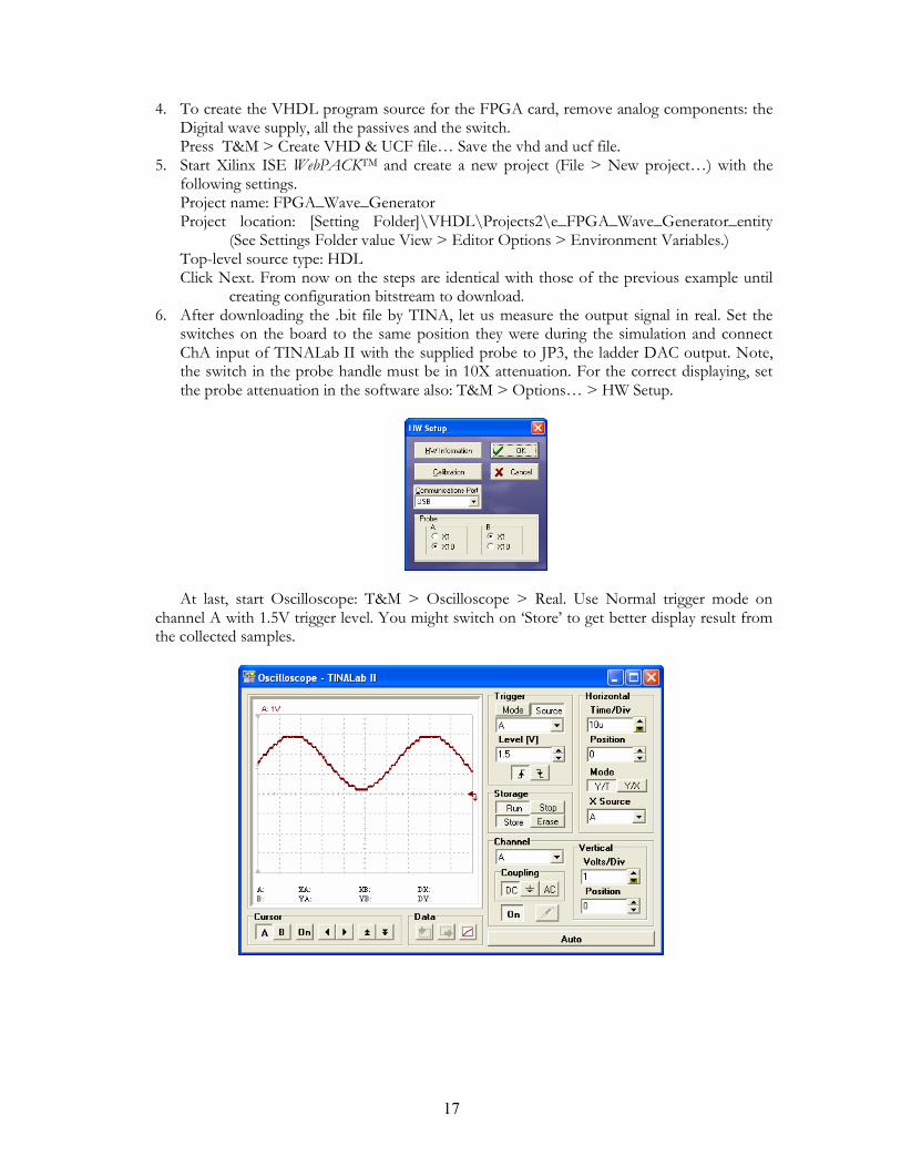
creating configuration bitstream to download. 6. After downloading the .bit file by TINA, let us measure the output signal in real. Set the
switches on the board to the same position they were during the simulation and connect ChA input of TINALab II with the supplied probe to JP3, the ladder DAC output. Note, the switch in the probe handle must be in 10X attenuation. For the correct displaying, set the probe attenuation in the software also: T&M > Options… > HW Setup.
At last, start Oscilloscope: T&M > Oscilloscope > Real. Use Normal trigger mode on channel A with 1.5V trigger level. You might switch on ‘Store’ to get better display result from the collected samples.

18
7. Stop the oscilloscope then click on the Export curves button. The Diagram Window will
come up. Copy the curves into the same diagram.
T
Measured
Simulated
0.00 25.00u 50.00u 75.00u 100.00u
A
0.00
4.00
Measured
Simulated
TINALab FPGA Quick Start REV. E
DesignSoft Inc. http://www.designsoftware.com