a proposed framework for measuring, identifying, and eliminating
TRANSCRIPT

Maxim > Design Support > Technical Documents > Application Notes > Basestations/Wireless Infrastructure > APP 4613Maxim > Design Support > Technical Documents > Application Notes > Communications Circuits > APP 4613Maxim > Design Support > Technical Documents > Application Notes > High-Speed Interconnect > APP 4613
Keywords: jitter, clock jitter, data jitter, high-speed serial, signal integrity, SERDES, serializer-deserializer, clockand data recovery, CDR, jitter tolerance, CPRI, common public radio interface, bit error rate, BER, deterministicjitter, random jitter
APPLICATION NOTE 4613
A Proposed Framework for Measuring, Identifying,and Eliminating Clock and Data Jitter on High-SpeedSerial Communication LinksBy: Hamed Sanogo, Field Applications Engineering ManagerMar 03, 2010
Abstract: As the new and successful serial-data standards go from fast to very fast, designers must devote agreater amount of time to the analog aspect of those high-speed signals. It is no longer enough to remain inthe digital domain with ones and zeros. To find and correct conditions that lead to potential problems, andthereby prevent those problems from showing up in the field, designers must also check the parametric realmof their designs. Signal integrity (SI) engineers must mitigate or eliminate the effects of timing jitter on systemperformance. The following discussion offers a simple and practical procedure for characterizing high-speedserial data links at 1Gbps and beyond.
A version of this application note appeared on the Electronic Design Magazine website, December 1, 2008.
IntroductionThe characterization of a high-speed serial link depends on the ability of the SI engineer to find, understand,and solve serious jitter problems. In this discussion, we assume that the clock and data recovery (CDR) blockof the PHY (physical layer) or SerDes (serializer-deserializer) device complies with the standards applicable tothat device. In a serial-communication system, the CDR recovers the clock signal from the data stream. Thus,a key operation is to extract data from the serial data stream and synchronize it with the data-transmitterclock.
The transmitter always contributes some jitter to the recovered clock, but we assume that contribution to beminimal. For simplification, therefore, we assume that any jitter seen on the recovered clock was coupled eitheronto the link in the cable (as EMI) or within the PCB (as crosstalk).
"Jitter transfer," "jitter tolerance," and "jitter generation" are important measures, but they apply more to PHYand SerDes devices than to the testing of system channels. We assume that the devices used in our designmeet all device-level compliance testing. We therefore focus on the complete system, as we find a way toreliably capture serial data at the receiver. We look at system-channel characterization rather than devicecharacterization. Such a channel (Figure 1) consists of the transmitter PHY, FR4 (PCB material), connector,
Page 1 of 18
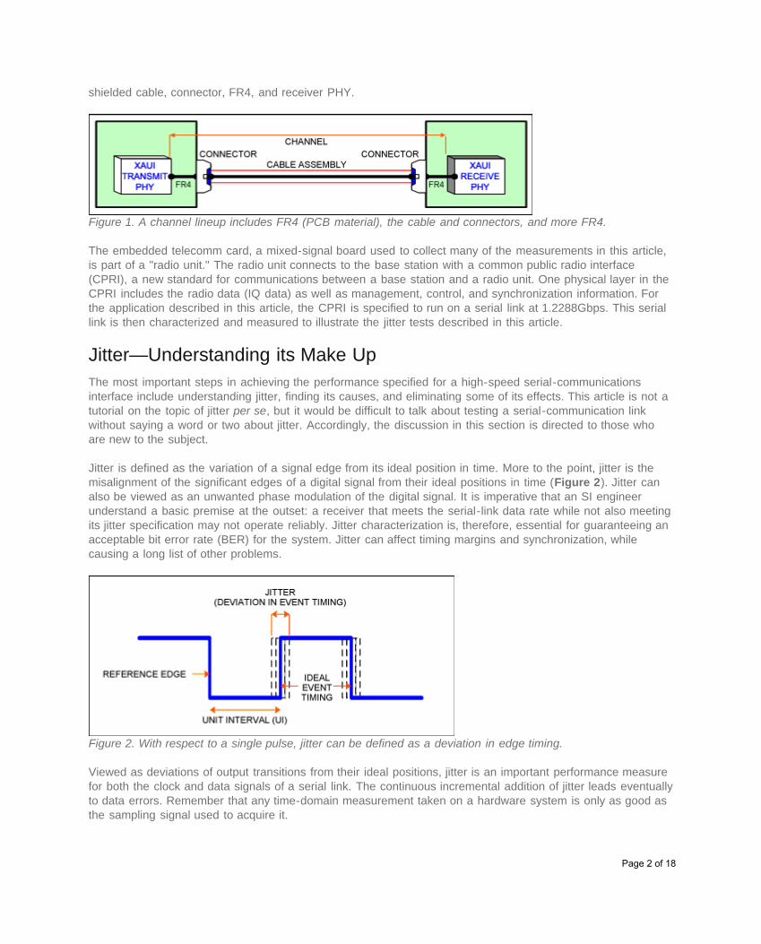
shielded cable, connector, FR4, and receiver PHY.
Figure 1. A channel lineup includes FR4 (PCB material), the cable and connectors, and more FR4.
The embedded telecomm card, a mixed-signal board used to collect many of the measurements in this article,is part of a "radio unit." The radio unit connects to the base station with a common public radio interface(CPRI), a new standard for communications between a base station and a radio unit. One physical layer in theCPRI includes the radio data (IQ data) as well as management, control, and synchronization information. Forthe application described in this article, the CPRI is specified to run on a serial link at 1.2288Gbps. This seriallink is then characterized and measured to illustrate the jitter tests described in this article.
Jitter—Understanding its Make UpThe most important steps in achieving the performance specified for a high-speed serial-communicationsinterface include understanding jitter, finding its causes, and eliminating some of its effects. This article is not atutorial on the topic of jitter per se, but it would be difficult to talk about testing a serial-communication linkwithout saying a word or two about jitter. Accordingly, the discussion in this section is directed to those whoare new to the subject.
Jitter is defined as the variation of a signal edge from its ideal position in time. More to the point, jitter is themisalignment of the significant edges of a digital signal from their ideal positions in time (Figure 2). Jitter canalso be viewed as an unwanted phase modulation of the digital signal. It is imperative that an SI engineerunderstand a basic premise at the outset: a receiver that meets the serial-link data rate while not also meetingits jitter specification may not operate reliably. Jitter characterization is, therefore, essential for guaranteeing anacceptable bit error rate (BER) for the system. Jitter can affect timing margins and synchronization, whilecausing a long list of other problems.
Figure 2. With respect to a single pulse, jitter can be defined as a deviation in edge timing.
Viewed as deviations of output transitions from their ideal positions, jitter is an important performance measurefor both the clock and data signals of a serial link. The continuous incremental addition of jitter leads eventuallyto data errors. Remember that any time-domain measurement taken on a hardware system is only as good asthe sampling signal used to acquire it.
Page 2 of 18

Today's serial-communication systems have opted to embed clock information in the data stream rather thanusing an external trigger signal at the receiver. The clock must, therefore, be recovered from the received bitstream itself. This function, known as CDR, is shown in the block diagram for a typical SerDes receiver(Figure 3). If, however, the incoming signal has more than a certain amount of jitter or phase noise, therecovered clock cannot stay accurately aligned with the data. Misalignment causes an inaccurate placement ofindividual data points in time.
Figure 3. This block diagram depicts a generic SerDes receiver.
To minimize the BER, you must properly time this phase shift with the data stream, and for that reason serial-communication standards now place a greater importance on highly accurate measurement of jitter. Jitter isgenerally classified as deterministic jitter (DJ) or random jitter (RJ). Because each type of jitter is createddifferently, they are characterized separately.
Two Fundamental Components of Jitter: DJ and RJRandom jitter represents timing noise with no discernable pattern. For the purpose of modeling, RJ is assumedto have a Gaussian probability distribution (Figure 4). Usually due to the forces of nature, RJ is statistical andunbounded. (It is characterized by its standard deviation value, expressed as an RMS quantity.) Thus, providingan RJ specification without a sample size does not make much sense. Other than measuring the value of RJin a system, however, most designers do little else with this parameter. (Finding the cause of RJ is a difficulttask, and beyond the scope of this article.)
Page 3 of 18

Figure 4. A Gaussian (normal) distribution is symmetrical with respect to the maximum value.
Deterministic jitter is caused by events in the system; it appears as timing noise with "somewhat" discernablepatterns. DJ is usually repeatable, persistent, and predictable. In addition, it is usually the result of faulty designin areas such as the circuit, the layout, and the transmission line. It is typically non-Gaussian, as is power-supply noise due to a bad reference plane.
Deterministic jitter is further classified into subcomponents: periodic jitter (PJ in Figure 5); data-dependent jitter(DDJ, also known as intersymbol interference, or ISI); duty-cycle-distortion jitter (DCDJ); and any other timingjitter that is uncorrelated and bounded to the data. PJ can be caused by crosstalk from other signals and fromsemiconductor switching close to the serial-data signals); by electromagnetic interference (EMI); and by otherunwanted modulation. DCDJ results from unbalanced transitions in the data (i.e., differences in rise and falltimes), and DDJ is jitter correlated with bit sequences in the data stream (also affected by the channel'sfrequency response).¹
Figure 5. For PJ, the timing deviations have a predictable pattern.
Page 4 of 18

Total Jitter (TJ)As you might guess, TJ is composed of random and deterministic components (Figure 6). There are severaltechniques for estimating TJ. Some find the TJ by resolving it into the RJ and DJ components, then addingthem together using a multiplier in front of the RJ component. Other methods find TJ by extrapolating thehistogram of time interval error (TIE) measurements. TJ is usually a peak-to-peak value expressed inpicoseconds or fractions of a unit interval (UI). For example, 0.2UI means that jitter is 20% of the data eye.
Figure 6. The total jitter in a system can include various types (components) as shown.
To predict the overall performance of a system, you must, therefore, understand the types of jitter and theireffects. Because jitter causes timing errors, it has become increasingly important to characterize and qualify alljitter components in a system. Before that can be done, however, you must determine the sources of jitter. Asmentioned earlier, the two types (random and deterministic) have different sources. A designer has little or nocontrol over the sources of RJ in an existing system of embedded circuit boards,² but good design practiceswill greatly mitigate or even eliminate the sources of DJ. Each jitter component has a specific cause, as shownin Table 1.¹
Table 1. Common Sources of Jitter
Jitter Type CommonSource Root Cause
Deterministic
EMI Unwanted radiation of conducted emissions from other devices in the PCB orsystem, such as a switching power supply.
Crosstalk Undesired signals that result from coupling between adjacent conductors.
ReflectionsImpedance mismatch (or mismatches) on the signal lineup (ISI from the receiver'sperspective), due to poor stubbing, incorrect or absent terminations, and/ordiscontinuities in the physical media.
Random
Shot noise White noise generated when electrons and holes move in a semiconductor (i.e.,noise within system components).
Flickernoise 1/f noise, mostly at lower frequencies.
Thermalnoise
White noise generated by the transfer of energy between free electrons and ions. Itis created by the movement and collision of electrons in the conductor.
Page 5 of 18

Six Steps to Achieve a Well-Characterized, High-Speed Serial LinkLink-Characterization FrameworkThe link-characterization framework presented here helps to identify and measure the sources of clock anddata jitter. The technique hinges on the designer's ability to separate jitter sources and to focus on the problemareas revealed by this testing framework. Jitter testing generally requires observation of a repeating test patternon the channel.
The data pattern to be used is important, because reflection and ISI are both data-dependent sources of noise.The test patterns used to collect the majority of plots in this paper included a mixed-frequency repeating K28.5sequence (also known as the comma character: K28.5 = 00111110101100000101), and a pseudo-random bitsequence (PRBS-23). PRBS patterns give a good spread of the different bit sequences that might be observedin actual data traffic. Other compliance test patterns for jitter evaluation are available, including the jitter testpattern (JTPAT), compliance random pattern (CRPAT), and compliance JTPAT (CJTPAT), to name a few.
The key to getting accurate measurements lies in selecting the right measurement equipment for yourapplication (oscilloscopes and probes, for instance). For step 1 of this framework (and for the remaining stepsas well), the signal is measured after it has propagated through a channel formed by a 50Ω transmission linethat also includes the cable, connector, and FR4 PCB. Solder to the PCB trace, as close as possible to thereceiver IC, a differential, high-performance probe with high bandwidth and low capacitive loading.
Step 1. Quantify Random and Deterministic Jitter (RJ and DJ)First, observe the signaling level. Then, collect link measurements and compare them to the standard. (Table 2gives an example of measurements versus the XAUI specification, which is a measurement of the PHY's inputcharacteristics.) The SI engineer can create a similar matrix for the standard against which a system is beingtested.
An eye diagram is one of the most important measurement tools to assess high-speed signal integrity. Itoverlays waveforms from multiple unit intervals (UIs), using either the real clock or a reconstructed clock as thetiming reference. Because the eye diagram helps you to visualize amplitude behavior as well as the timingbehavior of a waveform, it represents one of the most useful presentations of jitter. Figure 7 shows an eyediagram measurement taken from a XAUI channel.
Page 6 of 18

More detailed image (PDF, 1.4MB)Figure 7. This eye diagram (XAUI measurement) is displayed at the input of a PHY device.
Use timing-analysis software loaded on the scope (e.g., a TDSJIT3 from Tektronix®, for example). With thescope set for "golden PLL," the SI engineer can set the parameters shown in Table 2 and capture an eyediagram of the channel traffic. Then, the matrix shown in Table 2 can be completed for the particular standardbeing used. (Golden PLL is a method for filtering out jitter on the scope trigger, thereby ensuring that any jitterrepresented in the measured jitter amplitude and histograms is actually present on the link.³
Table 2. Measurements against the PHY Input Characteristics (Example)Input Characteristics Specification MeasurementsDifferential rise and fall times (TRF) ?
DJ tolerance 0.37UI TJ tolerance 0.65UI Differential amplitude (VP-P) 2.2VP-P (max)
Page 7 of 18

Step 2. Measure Amplitude Noise or Voltage Error HistogramsThis step measures amplitude noise, which can cause error in the design. We are looking to see if theprobability density functions (PDFs) for amplitude have a normal distribution for both the 1 and 0 levels.(Figure 8 shows the PDFs for an XAUI link.) The random-amplitude noise shown in blue in the histograms(circled in red) can be considered as normal distributions. The SI engineer can also use this plot as a graphicaid in determining whether other signaling issues are present, such as overshoot and undershoot. If amplitudenoise is an issue (if the amplitude histograms are bimodal, for example), then we likely have a power-distribution problem on the board.
More detailed image (PDF, 1.7MB)Figure 8. Voltage noise can be derived from an eye diagram as shown here.
Step 3. Compare Eye Diagram versus "Far-End" MasksStep 3 lets you to estimate the jitter quality for the received signal over a long sequence of data. Many jitterapplication packages include standard masks, whose minimum-closure dimension allows you to rate the qualityof the measured channel. By comparing the eye diagram to the receive masks, you can view the amount ofeye closure in a given configuration. The eye should be clear of the masks (Figures 9a and 9b).
Page 8 of 18

(a). More detailed image (PDF, 1.19MB)
(b). More detailed image (PDF, 1.31MB)Figure 9. By applying the XAUI far-end masks to a measured eye diagram, you can discern a bad case (a) anda good case (b).
At this stage, the tester also analyzes the eye plot's rising edges separately from the falling edges. In theexample of Figure 10, one can clearly observe that the rising and falling edges are not aligned in the middle atthe eye crossing point (the bimodal histogram circled at middle top of the figure). This bimodal histogramindicates the presence of cycle-to-cycle jitter or PJ on the channel. The histogram could also represent DCDor ISI jitter.
Page 9 of 18

More detailed image (PDF, 1.9MB)Figure 10. This data eye shows a bimodal histogram at the edge of the crossing.
Designers often limit their testing to a measurement of TJ and thus only view the histogram, which representsthe TJ (DJ and RJ mixed together). However, to understand the root cause of jitter and eliminate itscontributing components, it is essential to separate and identify each component. Since the eye diagram is ageneral tool that gives insight only into the amplitude and timing behavior of the signals, other means areneeded to separate the jitter components.
In the next step, we separate TJ into its components by analyzing the jitter histogram and bathtub plots.
Step 4. Separate Jitter Types and ComponentsTo keep jitter out of the system one must be able to separate the RJ and DJ components. The techniquedescribed in step 4 lets you distinguish these types of jitter, and helps with debugging and design verificationas well as characterization of the system links.
We now analyze some of the histograms collected in the previous sections.
Page 10 of 18
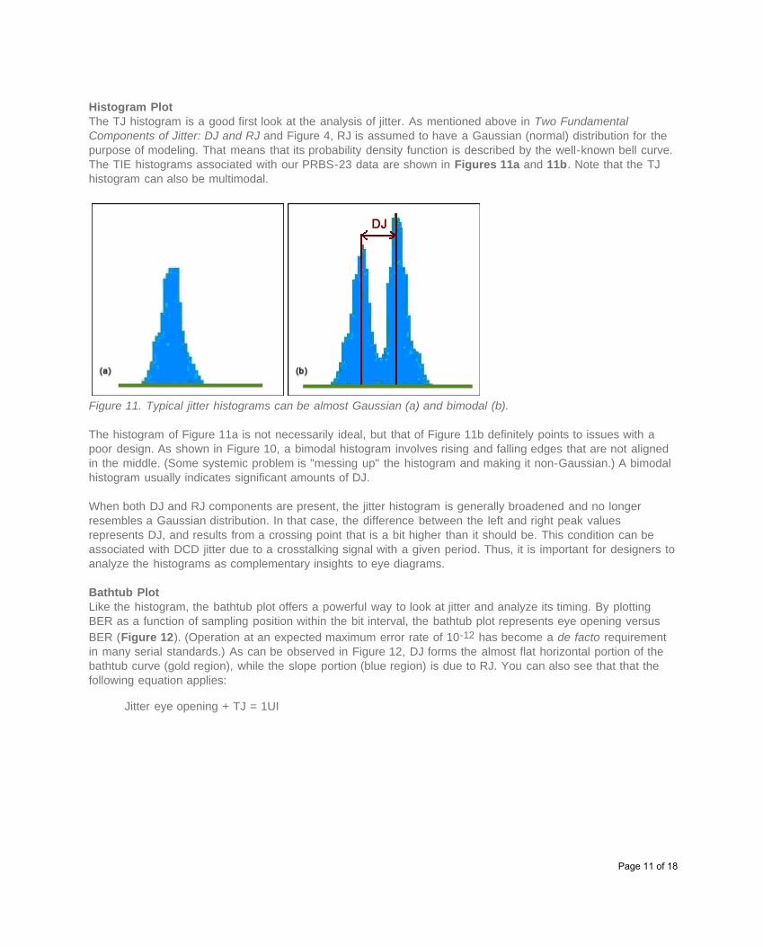
Histogram PlotThe TJ histogram is a good first look at the analysis of jitter. As mentioned above in Two FundamentalComponents of Jitter: DJ and RJ and Figure 4, RJ is assumed to have a Gaussian (normal) distribution for thepurpose of modeling. That means that its probability density function is described by the well-known bell curve.The TIE histograms associated with our PRBS-23 data are shown in Figures 11a and 11b. Note that the TJhistogram can also be multimodal.
Figure 11. Typical jitter histograms can be almost Gaussian (a) and bimodal (b).
The histogram of Figure 11a is not necessarily ideal, but that of Figure 11b definitely points to issues with apoor design. As shown in Figure 10, a bimodal histogram involves rising and falling edges that are not alignedin the middle. (Some systemic problem is "messing up" the histogram and making it non-Gaussian.) A bimodalhistogram usually indicates significant amounts of DJ.
When both DJ and RJ components are present, the jitter histogram is generally broadened and no longerresembles a Gaussian distribution. In that case, the difference between the left and right peak valuesrepresents DJ, and results from a crossing point that is a bit higher than it should be. This condition can beassociated with DCD jitter due to a crosstalking signal with a given period. Thus, it is important for designers toanalyze the histograms as complementary insights to eye diagrams.
Bathtub PlotLike the histogram, the bathtub plot offers a powerful way to look at jitter and analyze its timing. By plottingBER as a function of sampling position within the bit interval, the bathtub plot represents eye opening versusBER (Figure 12). (Operation at an expected maximum error rate of 10-12 has become a de facto requirementin many serial standards.) As can be observed in Figure 12, DJ forms the almost flat horizontal portion of thebathtub curve (gold region), while the slope portion (blue region) is due to RJ. You can also see that that thefollowing equation applies:
Jitter eye opening + TJ = 1UI
Page 11 of 18

Figure 12. This bathtub plot shows BER vs. decision time.
The measurement of a jitter histogram, or bathtub curve, or both, is a primary step informing the SI engineer ofjitter in the system. Neither measurement, however, reveals the individual sources of the jitter components. Inthe next step, we attempt to identify the root cause(s) of DJ by separating it into its components.
Step 5. Diagnose the Root Cause of JitterWe now analyze jitter in the frequency domain, which reveals DJ components (i.e., PJ, ISI, DCD, etc.) asdistinct single-frequency spurs (line spectra) that can be easily visualized to determine their sources. Thesefrequency domain views can include the phase-noise plot, the jitter spectrum plots, or a fast Fourier transform(FFT) of the jitter trend.
Jitter Spectrum of Data TIE PlotSeveral techniques are available for measuring jitter on a single waveform. One technique examines thespectrum of the TIE. TIE is the timing deviations of digital-data transitions from their ideal (jitter-free) locations.(See prior section on Total jitter.) In short, the TIE measures how far each active edge of the clock varies fromits ideal position. TIE is important because it shows the cumulative effect of even a small amount of jitter³ overtime.
We now return to the serial link being characterized. Figure 13 shows a plot of the jitter spectrum of the TIEtaken on the link. In the figure the spurs present a snapshot of the channel at a specific point in time. Thespurs have been numbered F1, F2, F3, and F4. The first spur is at F1 = 61.44MHz (the fundamental frequencyof the recovered clock). Spurs F2 and F4 are integer multiples (harmonics) of F1. Spur F3 is at 153.18MHzdoes not seem to fit in because there is no clock source on the board with this frequency. F3 represents anintermodulation of two or more frequencies on the card. It could also be produced when the high-speed signalcrosses over a split in the power/ground plane. When high-speed signals pass over a split reference plane, thediscontinuity in the return path for current can create emissions.
Page 12 of 18

Figure 13. A spectrum of TIE for this data reveals four significant spurs of PJ.
Spectral AnalysisTo reveal sources of jitter, the SI engineer must conduct a spectral analysis of the jitter spectrum plot todetermine an idea of the modulation frequency of each jitter source. Frequency-domain plots exhibit the uniquefrequency spurs. You can isolate certain DJ components using the following methods:
Isolating PJOccasionally the serial data channel will show a nice looking histogram (a Gaussian distribution), yet thespectrum of TIE on the same link shows some spurs. This means that a small PJ can be buried in the RJ andnot be visible on the histogram of TJ. It is, therefore, worthwhile to do the spectral analysis to eliminate allsources of jitter, even when the jitter numbers have not gone out of spec.
In the spectrum plot analysis in Figure 13, F3 was regarded as the result of an unwanted modulation. It is thistype of unwanted modulation (due to EMI or crosstalk, for instance) that usually causes PJ. The signature ofPJ is that it repeats at a fixed frequency. Such unwanted modulation can also be caused by cross-coupling,such as switching noise from the power-supply module coupling into the data or system clock.
Isolating duty Cycle Distortion (DCD)DCD points to differences in the rise and fall times of the digital transitions and to variations in switchingthresholds for the devices previously mentioned. DCD is caused both by voltage offsets between differentialinputs and by differences in the system's rise and fall times. The rise and fall edges in Figure 9, for example,are not aligned in the middle. An SI engineer can attempt to isolate DCD by stimulating the system with ahigh-frequency pattern such D21.5 (1010101010...). That pattern is effective in showing DCD while eliminatingISI.
Isolating ISIA common source of DDJ is the frequency response of the signal path through which the serial data istransmitted. ISI is a type of DDJ. It is created in the channel lineup that includes the cable and connectors; it isaffected by losses in the FR4 PCB material. Because ISI is usually the result of a bandwidth limitation in eitherthe transmitter or the signal path, limited rise and fall times in the signals can produce varying amplitudes for
Page 13 of 18

the data bits.³ Another primary source of DDJ is impedance mismatch in the channel lineup due to an impropertermination of the bus. Reflections caused by a transmission line with mismatched termination impedance cancause delays and/or attenuation of the transmitted signals.
Step 6. Optimizing Tx Preemphasis and Rx EqualizationIt is well established that the amount of attenuation caused by lossy FR4 traces on a PCB depends on thesignaling speed and the length of the transmission medium. In short, FR4 losses are more severe at the higherswitching frequencies. Preemphasis and equalization can mitigate the effects of signal attenuation anddegradation, thereby restoring the original signal. This link-optimization step not only applies to designs withPHY devices that support transmitter preemphasis and receiver equalization, but also to discrete ICs forpreemphasis and equalization which can be used to compensate for the transmission losses caused by FR4material. Step 6 applies to designs that include provision for tuning the preemphasis and equalization levels ofSerDes/PHY devices. We therefore assume that the system in question includes such provisions.
Optimal PreemphasisPreemphasis is a signal-improvement technique that opens the eye pattern at the far end of a cable (at thereceiver). In general, preemphasis increases the transmitted signal quality by increasing the magnitude of somefrequencies with respect to the magnitude of other (usually lower) frequencies. The key is to find the optimalpreemphasis setting for the design.
For SerDes and PHY devices that support different levels of preemphasis, the SI engineer can step throughthe levels and select the one with the best eye or the one that achieves a BER of 10-12 or better. Alsoavailable are preemphasis driver ICs like the MAX3982 that can be used to optimize performance by manuallytuning the transmitter with respect to eye opening and ISI jitter at the receiver.
There is a slight advantage to using a discrete preemphasis IC versus one that is embedded in a SerDes/PHYdevice: the tester can capture an eye diagram at the receiver input with a scope and quickly see improvementsin the signal quality. In simple terms, the wider the eye, the better the quality. The SI engineer should,therefore, look for the best eye opening using the least amount of preemphasis. The rule is: do notpreemphasize too much. An optimal setting should provide some improvements in the channel's overall jitterperformance.
Optimal EqualizationBesides adding preemphasis, you can also minimize the effects of ISI by optimizing the equalization setting atthe receiver. The equalizer removes and/or overcomes the effects of high-frequency attenuation introduced onthe waveform while traveling on the PCB and cable. The receiver's equalizer compensates the received signalfor dielectric and skin losses in the PCB material, as well as for high-frequency loss in the cable.
In the practical and experimental sense, the effects of received equalization are difficult to evaluate when thatfunction is embedded in a SerDes or PHY device. External receiver-equalizer ICs like the MAX3784 canprovide a way to quickly observe the results of receiver equalization on the scope (as opposed to BER testingfor a SerDes). Figure 14 shows the MAX3784 equalizer's input eye diagram before and after equalization at asignaling rate of 5Gbps. These measurements were made on a 40in, 6 mil trace (stripline) on FR4 PCBmaterial.
Page 14 of 18
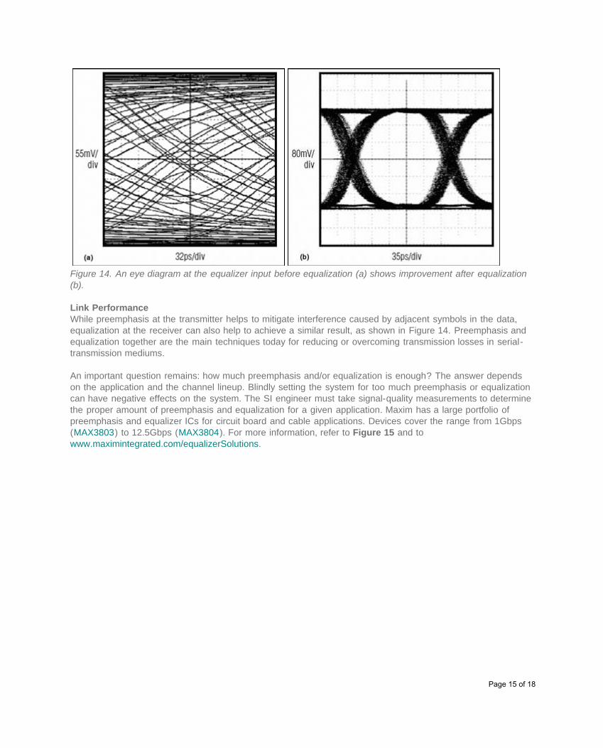
Figure 14. An eye diagram at the equalizer input before equalization (a) shows improvement after equalization(b).
Link PerformanceWhile preemphasis at the transmitter helps to mitigate interference caused by adjacent symbols in the data,equalization at the receiver can also help to achieve a similar result, as shown in Figure 14. Preemphasis andequalization together are the main techniques today for reducing or overcoming transmission losses in serial-transmission mediums.
An important question remains: how much preemphasis and/or equalization is enough? The answer dependson the application and the channel lineup. Blindly setting the system for too much preemphasis or equalizationcan have negative effects on the system. The SI engineer must take signal-quality measurements to determinethe proper amount of preemphasis and equalization for a given application. Maxim has a large portfolio ofpreemphasis and equalizer ICs for circuit board and cable applications. Devices cover the range from 1Gbps(MAX3803) to 12.5Gbps (MAX3804). For more information, refer to Figure 15 and towww.maximintegrated.com/equalizerSolutions.
Page 15 of 18

Figure 15. Guide for selecting a preemphasis/equalizer ICs are shown as a function of data rate and signal-path length, for circuit boards and cables.
ConclusionIf you design a high-speed digital system today, chances are that you will have a jitter spec or a jitter budget tomeet. Understanding jitter and its causes allows you to create high-performance systems. The accurateseparations of TJ into RJ and DJ, and DJ into its subcomponents (PJ, DCD, ISI), are imperative for compliancewith the serial standard. Understanding jitter in its complexity is also important in providing diagnosticinformation for improving the design.
Designers must ensure that their designs work for reasons of competitive advantage, but they must also knowthe point at which their design stops working. By identifying jitter and its sources, the link-characterizationframework proposed in this paper (see Figure 16) should help to improve system performance.
Page 16 of 18

Figure 16. The proposed framework for measuring, identifying, and eliminating clock and data jitter comprisessix steps.
References¹Jitter fundamentals, "Enhance Speed, Throughput and Accuracy with One Powerful Instrument," Wavecrest: ATechnologies Company, Eden Prairie, Minnesota, available at www.wavecrest.com.
²The SI engineer can control RJ by a careful selection of the components used. That approach is used tocontrol the effect of RJ on PLL designs.
³A Guide to Understanding and Characterizing Timing Jitter, Tektronix Enabling Innovation Primer, available atwww.tektronix.com/jitter.
Tektronix is a registered trademark and registered service mark of Tektronix, Inc.
Related Parts
MAX3784 5Gbps PCB Equalizer Free Samples
MAX3803 DC-Coupled, UCSP 3.125Gbps Equalizer
Page 17 of 18
MAX3804 12.5Gbps Settable Receive Equalizer Free Samples
MAX3892 +3.3V, 2.5Gbps/2.7Gbps, SDH/SONET 4:1 Serializer withClock Synthesis
Free Samples
More InformationFor Technical Support: http://www.maximintegrated.com/supportFor Samples: http://www.maximintegrated.com/samplesOther Questions and Comments: http://www.maximintegrated.com/contact
Application Note 4613: http://www.maximintegrated.com/an4613APPLICATION NOTE 4613, AN4613, AN 4613, APP4613, Appnote4613, Appnote 4613 Copyright © by Maxim Integrated ProductsAdditional Legal Notices: http://www.maximintegrated.com/legal
Page 18 of 18