a novel low-temperature growth method of silicon
TRANSCRIPT
i
i
A Novel Low-Temperature Growth Method
of Silicon Structures and Application in
Flash Memory
Thomas Attia Mih
B.Sc., M.Sc. (Physics)
A Thesis Submitted to De Montfort University, Leicester for
the Degree of
Doctor of Philosophy (PhD)
Emerging Technologies Research Centre, De Montfort
University, Leicester, UK
August 2011

ii
ii
To My Beloved Mother (Ze-Attia)
Francisca Mbong
And
My Eternally Resting Father
Simon Mih
After climbing a great hill, one only finds that there are many
more hills to climb (Nelson Mandela)

iii
iii
Declaration
This thesis contains results of research undertaken solely by the author between
October 2007 and March 2011 in the Emerging Technologies Research Centre of the
Faculty of Technology, De Montfort University, Leicester, under the supervision of Drs.
Shashi Paul and Richard Barrie Michael Cross. The research is entirely the original
work of the author and contains nothing done in collaboration with another person or
institution except where explicit acknowledgement is given.
The work has not been submitted in whole or in part for any other University
degree or diploma.
Permission to copy or use whole or part of the work contained herein must be
solicited except for the purpose of private study or academic purposes in which case the
author must be explicitly acknowledged.
Signature of Author:
Thomas Attia Mih
Leicester, August 2011
iv
iv
Abstract
Flash memories are solid-state non-volatile memories. They play a vital role
especially in information storage in a wide range of consumer electronic devices and
applications including smart phones, digital cameras, laptop computers, and satellite
navigators. The demand for high density flash has surged as a result of the proliferation
of these consumer electronic portable gadgets and the more features they offer –
wireless internet, touch screen, video capabilities.
The increase in the density of flash memory devices over the years has come as
a result of continuous memory cell-size reduction. This size scaling is however
approaching a dead end and it is widely agreed that further reduction beyond the 20 nm
technological node is going to be very difficult, as it would result to challenges such as
cross-talk or cell-to-cell interference, a high statistical variation in the number of stored
electrons in the floating gate and high leakage currents due to thinner tunnel oxides.
Because of these challenges a wide range of solutions in form of materials and
device architectures are being investigated. Among them is three-dimensional (3-D)
flash, which is widely acclaimed as the ideal solution, as they promise the integration of
long-time retention and ultra-high density cells without compromising device reliability.
However, current high-temperature (>600 °C) growth techniques of the Polycrystalline
silicon floating gate material are incompatible with 3-D flash memory; with vertically
stacked memory layers, which require process temperatures to be ≤ 400 °C. There
already exist some low-temperature techniques for producing polycrystalline silicon
such as laser annealing, solid-phase crystallization of amorphous silicon and metal-
induced crystallization. However, these have some short-comings which make them not
suitable for use in 3-D flash memory, e.g. the high furnace annealing temperatures (700
°C) in solid-phase crystallization of amorphous silicon which could potentially damage
underlying memory layers in 3-D flash, and the metal contaminants in metal-induced
crystallization which is a potential source of high leakage currents. There is therefore a

v
v
need for alternative low-temperature techniques that would be most suitable for flash
memory purposes.
With reference to the above, the main objective of this research was to develop
a novel low temperature method for growing silicon structures at ≤ 400 °C. This thesis
thus describes the development of a low-temperature method for polycrystalline silicon
growth and the application of the technique in a capacitor-like flash memory device.
It has been demonstrated that silicon structures with polycrystalline silicon-like
properties can be grown at ≤ 400 °C in a 13.56 MHz radio frequency (RF) plasma-
enhanced chemical vapour deposition (PECVD) reactor with the aid of Nickel Formate
Dihydrate (NFD). It is also shown that the NFD coated on the substrates, thermally
decomposes in-situ during the deposition process forming Ni particles that act as
nucleation and growth sites of polycrystalline silicon. Silicon films grown by this
technique and without annealing, have exhibited optical band gaps of ~ 1.2 eV
compared to 1.78 eV for films grown under identical conditions but without the
substrate being coated. These values were determined from UV-Vis spectroscopy and
Tauc plots. These band gaps correspond to polycrystalline silicon and amorphous
silicon respectively, meaning that the films grown on NFD-coated substrates are
polycrystalline silicon while those grown on uncoated substrates remain amorphous.
Moreover, this novel technique has been used to fabricate a capacitor-like flash memory
that has exhibited hysteresis width corresponding to charge storage density in the order
of 1012
cm-2
with a retention time well above 20 days for a device with silicon films
grown at 300 °C. Films grown on uncoated films have not exhibit any significant
hysteresis, and thus no flash memory-like behaviour. Given that all process
temperatures throughout the fabrication of the devices are less than 400 °C and that no
annealing of any sort was done on the material and devices, this growth method is
thermal budget efficient and meets the crucial process temperature requirements of 3-D
flash memory. Furthermore, the technique is glass compatible, which could prove a
major step towards the acquisition of flash memory-integrated systems on glass, as well
as other applications requiring low temperature polycrystalline silicon.

vi
vi
Acknowledgement
Foremost, I would like to acknowledge with gratitude De Montfort University
for financial assistance over 36 months of this research. Besides the University, my
utmost thanks go to my Supervisors Drs. Shashi Paul and Richard Barrie Michael Cross
for their advice, encouragement and patience throughout my research period and for
painstakingly and critically reading over my written works with invaluable suggestions;
Dr. Konstantin Vershinin for his support and encouragement and critical examination of
my work throughout all stages of my research years, Dr. Iulia Salaoru for her support on
polymer dielectrics, Dr. Dominic Charles Prime for his support and advice on AFM,
Mr. Paul Taylor, the EMTERC Senior Technician for taking care of malfunctioning
equipment in the research centre throughout my research period, Prof. Anjana Devi for
organizing the growth of zirconia dielectric films in her laboratory.
My appreciation also goes to Dr. Divine Ngwashi Khan, Dr. David Black and
Miss Nare Gabrielyan for the light-hearted moments we shared in the research centre.
It is a great opportunity for me to express my profound gratitude to my entire
family, especially to my mother Mama Francisca Mbong for all her love and care; my
brother, Prof. Afui Mathias Mih for his continuous encouragement and financial
assistance; my sister, Angela Yuoh Mih who accepted God’s call to eternity and did not
live to see the end of what she had encouraged me to undertake; all my sisters Emilia,
Christina, Grace for their love and encouragement; my nephews and nieces and all other
family members whose names have not been mentioned for their love.
A special thank you to my wife, Loveline Ekei Mih for her love and support.
I would sincerely like to thank every other person not mentioned who has
contributed in any way to the successful realization of this work.
Above all, I thank God Almighty and give Him glory for everything.

vii
vii
Table of Contents
Declaration ______________________________________________________ iii
Abstract ________________________________________________________ iv
Acknowledgement _________________________________________________ vi
Table of Contents ________________________________________________ vii
Table of Figures ________________________________________________ xii
Chapter 1. An Overview of Research ________________________________ 1
1.1 Introduction ____________________________________________ 1
1.2 Research Objectives _____________________________________ 5
1.3 Thesis structure _________________________________________ 6
1.4 Publications and Conferences _____________________________ 6
1.4.1 Referenced Works _____________________________________ 6
1.4.2 Oral and Poster Presentations ____________________________ 7
1.4.3 Submitted Journals ____________________________________ 7
Chapter 2. Flash Memory and Related Emerging Storage Devices ________ 9
2.1 Introduction ____________________________________________ 9
2.1.1 Hard Disc Drive and Solid-State Drive ____________________ 10
2.1.2 Random Access Memory (RAM) ________________________ 12
2.1.3 Read Only Memory (ROM) ____________________________ 13
2.1.4 Non-Volatile RAM ___________________________________ 14
2.2 Brief Historical Evolution of Floating Gate Non-Volatile Memory
15
2.3 Flash Memory Overview ________________________________ 20
2.3.1 Flash Memory Cell Structure ___________________________ 21
2.3.2 The Capacitor Model and Equations of the FG MOS Device ___ 22
2.3.3 Working Mechanisms of Flash Memory Cell _______________ 26
2.3.3.1 Channel Hot Electron Injection ___________________________ 27

viii
viii
2.3.3.2 Fowler-Nordheim Tunnelling _____________________________ 29
2.3.3.3 Reading Operation _____________________________________ 31
2.3.4 Reliability __________________________________________ 31
2.3.4.1 Write/Erase Cycle Endurance ____________________________ 32
2.3.4.2 Retention _____________________________________________ 33
2.3.4.3 Cell Disturb __________________________________________ 34
2.4 Flash Memory Challenges _______________________________ 36
2.5 Emerging Universal Memory Technologies _________________ 40
2.5.1 Phase Change Memory ________________________________ 41
2.5.2 Magnetoresistive Random Access Memory ________________ 43
2.5.3 Ferroelectric RAM (FeRAM) ___________________________ 45
2.5.4 Organic Memory Devices (OMD) _______________________ 48
2.6 Three-Dimensional Flash Memory ________________________ 50
2.6.1 Different 3-D Memory Cell Designs ______________________ 51
2.7 Summary _____________________________________________ 56
Chapter 3. Overview of Low-Temperature Methods of Obtaining
Polycrystalline Silicon ____________________________________________ 57
3.1 Introduction ___________________________________________ 57
3.2 Structure and Electronic Properties of Polycrystalline silicon __ 57
3.3 Growth Methods of Polycrystalline silicon __________________ 60
3.4 Plasma-enhanced Chemical Vapour Deposition (PECVD) _____ 62
3.4.1 The Capacitively Coupled RF PECVD Reactor Design _______ 63
3.5 Deposition of a-Si or a-Si:H ______________________________ 65
3.6 Conversion of a-Si and a-Si:H to Polycrystalline silicon _______ 66
3.6.1 Solid-Phase Crystallization _____________________________ 67
3.6.2 Laser Annealing _____________________________________ 68
3.6.3 Metal-Induced (Lateral) Crystallization ___________________ 71
3.6.4 Advantages and Disadvantages of MIC, MILC SPC, and ELA of
a-Si Techniques ___________________________________________________ 73
ix
ix
3.7 Summary _____________________________________________ 74
Chapter 4. Characterization Methods of Silicon Films and Memory Devices
75
4.1 Introduction ___________________________________________ 75
4.2 Physical Characterization _______________________________ 75
4.2.1 Film Thickness Measurement ___________________________ 76
4.2.1.1 Ellipsometry __________________________________________ 76
4.2.1.2 Step Profilometry ______________________________________ 79
4.2.2 Fourier Transform Infrared Spectroscopy (FTIR) ___________ 81
4.2.3 Ultra-Violet Visible (UV-Vis) Spectroscopy _______________ 84
4.2.4 Atomic Force Microscopy (AFM) _______________________ 87
4.3 Electrical Characterisation ______________________________ 90
4.3.1 Dark- and Photoconductivity ___________________________ 90
4.3.2 Electrical Characterization of MIS and MIM Devices ________ 92
4.4 Summary _____________________________________________ 93
Chapter 5. Dip-Coating and FTIR Investigation of Nickel Formate dihydrate
95
5.1 Introduction ___________________________________________ 95
5.2 Basic Properties of Nickel Formate Dihydrate _______________ 96
5.3 Dip-Coating of NFD ____________________________________ 97
5.3.1 The Nima Dip-Coater System ___________________________ 98
5.3.2 Preparation of Precursor Solution ________________________ 99
5.3.3 Choosing the Better Solvent ___________________________ 100
5.3.3.1 Spin coating _________________________________________ 100
5.3.3.2 Squirting ____________________________________________ 101
5.3.3.3 Complete Submersion Coating ___________________________ 101
5.3.3.4 Results______________________________________________ 102
5.4 The Dip Coating Process _______________________________ 104

x
x
5.4.1 Effect of Immersion Time on the Thickness of NFD Coating on
Substrate 106
5.4.2 Variation of Thickness with Withdrawal Speed ____________ 107
5.4.3 Variation of Thickness with NFD Solution Temperature _____ 108
5.4.4 Discussion on Observed Effects of Coating Parameters on
Thickness of Coating______________________________________________ 108
5.5 FTIR of Nickel Formate Dihydrate _______________________ 111
5.6 Summary ____________________________________________ 113
Chapter 6. Silicon Structures: PECVD Growth and Optimization _______ 115
6.1 Introduction __________________________________________ 115
6.2 Silicon Films Growth Procedure _________________________ 116
6.3 Effects of Deposition Parameters on Silicon Films Properties _ 118
6.3.1 Temperature Effects _________________________________ 118
6.3.1.1 Band Gap ___________________________________________ 119
6.3.1.2 Hydrogen Content ____________________________________ 120
6.3.1.3 Photo- and Dark Conductivity ___________________________ 121
6.3.1.4 Film Surface Roughness and surface grain size ______________ 122
6.3.2 Effect of RF Power Variation __________________________ 124
6.3.3 Effects of Changes in Silane Flow Rate __________________ 126
6.4 Contamination ________________________________________ 127
6.5 Deposition of Silicon Nitride Dielectric ____________________ 130
6.6 Summary of Chapter 6 _________________________________ 134
Chapter 7. Memory Behaviour of NFD-assisted Grown Silicon Structures
135
7.1 Introduction __________________________________________ 135
7.2 Fabrication of MIS Devices _____________________________ 135
7.2.1 Deposition of Gate Insulator ___________________________ 136
7.2.1.1 Polystyrene and Polyvinyl Acetate ________________________ 137
7.2.1.2 Silicon Nitride ________________________________________ 137

xi
xi
7.2.2 Evaporation of Gate Electrodes _________________________ 137
7.3 Charge storage in MIS Devices __________________________ 139
7.4 Memory Characteristics ________________________________ 145
7.4.1 Leakage Current ____________________________________ 145
7.4.2 Memory Window ___________________________________ 146
7.4.3 Programme/Erase, Retention and Endurance ______________ 147
7.5 Summary ____________________________________________ 150
Chapter 8. Conclusion and Recommendations for Further Research ____ 151
8.1 Introduction __________________________________________ 151
8.2 Major Results ________________________________________ 151
8.3 Recommendation for Further Studies _____________________ 153
8.3.1 Dip-coating of NFD _________________________________ 153
8.3.2 Contamination of Si Films ____________________________ 153
8.3.3 Memory ___________________________________________ 154
References _____________________________________________________ 155
Appendices _____________________________________________________ 181
Appendix 1: Substrate Cleaning ______________________________ 181
8.3.4 Corning Glass Substrates _____________________________ 181
8.3.5 Crystalline Silicon ___________________________________ 181
8.3.6 Plasma Cleaning of Substrates _________________________ 181
Appendix 2: The PECVD System _____________________________ 183
Appendix 3: Supplementary AFM DATA ______________________ 184
xii
xii
Table of Figures
Figure 2-1: Semiconductor memory tree ...................................................................... 9
Figure 2-2: The hard disc drive (HDD)[62] ................................................................ 10
Figure 2-3: Illustration of (a) DRAM and (b) SRAM[66] ......................................... 13
Figure 2-4: Cell connections in (a) NOR flash and (b) NAND flash memory devices
................................................................................................................................. 15
Figure 2-5: metal-insulator-metal-insulator-semiconductor (MIMIS) FG device. . 16
Figure 2-6: Diagrammatic representation of (a) The MNOS cell, (b) the FAMOS
cell and (c) the SAMOS cell. ................................................................................. 17
Figure 2-7: The Electrically Erasable programmable ROM (EEPROM) with a
select transistor ...................................................................................................... 18
Figure 2-8: Cell structure of the (a) Silicon-Nitride-Oxide-Semiconductor (SNOS)
and (b) Silicon-Oxide-Nitride-Oxide-Semiconductor (SONOS) devices. The
MOS select transistor is not shown...................................................................... 20
Figure 2-9: The basic cell structure of (a) the MOSFET and (b) the FG flash
memory cell. ........................................................................................................... 22
Figure 2-10: Illustration of the capacitance model of the FG memory cell. ............ 22
Figure 2-11: I-V characteristics of the FG MOS device at the neutral "1" and
charged "0" states. The threshold voltage shift ∆Vt is proportional to the
charge stored in the FG. ∆Vt is also known as the memory window. ............... 25
Figure 2-12: (a) Schematic illustration of channel hot electron (CHE) injection
programming and (b) the potential energy diagram of CHE versus vertical
distance from control gate. ................................................................................... 27
Figure 2-13: Schematic illustration of Fowler-Nordheim (F-N) tunnelling (a)
Programming and (b) Erase with corresponding electron energy diagrams
against vertical distance from control gate. ........................................................ 30
Figure 2-14: An illustration of cell disturbs in an array of flash memory cells. The
shaded cell is being programmed while cell disturb occurs in the other cells in
the same wordline (row) and bitline (column). ................................................... 35
Figure 2-15: Graph of flash memory cell area achieved within the decade 2000-
2010, illustrating flash memory scaling. .............................................................. 36

xiii
xiii
Figure 2-16: An illustration of the phase change random access memory with the
coresponding schematic 1T1R circuit representation ....................................... 42
Figure 2-17: Illustrations of the 1T1R Magnetoresistive RAM showing the
magnetic tunnel junction MTJ in the antiparallel (high resistance “1” state)
and parallel states (low resistance “0” state)[141]. ............................................ 44
Figure 2-18: Illustration of the lead zirconate titanate (PZT) structure[150]. ........ 46
Figure 2-19: Illustration of the polarization behaviour of the ferroelectric PZT
with applied electric field...................................................................................... 47
Figure 2-20. Schematic diagram of organic memory devices ................................... 49
Figure 2-21: Illustration of different shapes of I-V characteristics of polymer
memory devices: (a) N-Shaped, (b) O-shaped, (c) Symmetric S-Shaped and (d)
asymmetric S-Shaped [29]. ................................................................................... 50
Figure 2-22. Illustrations of the TCAT, P-BICS, VSAT and VG 3-D-type flash
memories[178] ....................................................................................................... 52
Figure 2-23 : Schematic Illustration of the 3-D cell array transistors (3-D CAT) (a)
Gate all around (GAA-CAT), (b) Double Gate (DG-CAT) (c) FinFET (Fin-
CAT)[179] .............................................................................................................. 54
Figure 2-24: (I) An illustration of the V-groove MOSFET transistor device process
flow: (a) handling and device wafers; (b) low temperature bonding; (c) Si
removal and texturing of buried oxide; (d) Si anisotropic etching and buried
oxide stripping. (II) V-groove 3-D NVM transistor ........................................... 55
Figure 3-1: Illustration of (a) FCC Structure of a unit cell of silicon and (b) poly-Si
crystal grains separated by grain boundaries. ................................................... 58
Figure 3-2: Schematic diagram of the Master Unit (PECVD unit) of the
Master/Slave PlasmaLab reactor system ............................................................ 65
Figure 3-3. Illustration of laser annealing of a-Si film ............................................... 70
Figure 3-4: Illustration of the MIC and MILC processes ......................................... 72
Figure 4-1: An illustration of reflection and refraction of light in a 3-layer
structure. The ambient is air of refractive index 1, the middle layer is the
deposited thin film of complex refractive index n1 and the lower layer is the
substrate of complex refractive index n2 ............................................................. 77
Figure 4-2. Illustration of the layout of a single wavelength ellipsometry (SWE) .. 79
xiv
xiv
Figure 4-3: Schematic illustration of the step profilometry showing the direction in
which measurements were performed and the expected step profile............... 81
Figure 4-4: Illustration of the Michelson Interferometer, an important component
in FTIR ................................................................................................................... 82
Figure 4-5: Inner view of the UV-Vis spectrophotometer (model: Evolution 300).
The red lines are the beam of light[297] ............................................................. 86
Figure 4-6: Illustration of the beam deflection system of the AFM. A position
sensitive photodiode is used to measure the position of the beam. On the right
is the Force against distance z of probe from the sample surface .................... 88
Figure 4-7: Schematic diagram of gap-cell device for measuring photo- and dark
conductivity. The Al electrodes were evaporated onto the silicon films grown
on glass substrates using gap-cell shadow masks with gap lengths shown on
diagram. ................................................................................................................. 92
Figure 4-8: Set up of the electrical measurement system .......................................... 93
Figure 5-1: An illustration of the Nima precision dip-coater system. ...................... 98
Figure 5-2: Optical band gap variation with concentration of NFD in methanol and
in water ................................................................................................................. 103
Figure 5-3: Variation of NFD coating thickness with immersion time for 20 and 30
mg ml-1
NFD solutions each at 30 °C. The withdrawal speed was 1 mm min-1
.
............................................................................................................................... 107
Figure 5-4: Thickness variation with withdrawal speed at constant immersion time
of 5 min, solution temperature of 30 °C and concentration of 20 mg ml-1
. .... 107
Figure 5-5: (a) Thickness variation with temperature and (b) Average roughness
variation with Temperature of NFD solution at constant immersion time of 5
min and withdrawal speed of 1 mm min-1
. ........................................................ 108
Figure 5-6: (a) lnd variation with reciprocal of immersion time for experimental
results obtained with the 20 mg ml-1 solution and (b) Thickness variation with
immersion time for experimental and fitted data. ........................................... 111
Figure 5-7: FTIR absorption spectra for (a) as-coated NFD on p-type silicon
substrate, and (b) for calcined NFD coated substrates at 250, 300 and 400 °C
showing the formate vibration mode region between 1200 and 2000 cm-1
.... 112
Figure 6-1: variation of film properties with growth temperature. ....................... 119

xv
xv
Figure 6-2: AFM micrographs of Silicon structures showing surface grains grown
at 400 °C on NFD-coated substrates. ................................................................. 123
Figure 6-3: AFM 3-D topography micrographs showing films grown at different
temperatures. The left column is for micrographs of films on uncoated p-Si
substrates while the right column is for NFD-coated substrates. Rows 1-3
running from top to bottom are for films grown at 250, 300 and 400 °C
respectively........................................................................................................... 124
Figure 6-4: Graphs showing variation of film properties with RF power. ............ 125
Figure 6-5: Variation of film properties with changes in silane flow rate. ............ 127
Figure 6-6: FTIR spectra illustrating the effect of film deposition temperature on
the oxygen content of the film. Films were grown at a pressure of 200 mtorr,
RF power of 5W and silane flow rate of 50 sccm. ............................................ 128
Figure 6-7: Variation in growth rate and index of refraction for silicon nitride
films with changes in the ratio R of silane flow rate to ammonia flow rate.
Films were grown at a temperature of 300 °C, RF power of 50W, nitrogen
flow of 100 sccm and ammonia flow of 40 sccm while silane flow was changed
to change R. ......................................................................................................... 131
Figure 6-8: FTIR spectra to show the effects on absorption peak heights of the N-H
and Si-H vibration modes for different R values. ............................................ 132
Figure 6-9: C-V curves of Si3N4 MIS for films grown at (a) high silane to ammonia
flow ratio of 0.275 and (b)low silane to ammonia flow ratio of 0.165 ............ 133
Figure 6-10: Graphs showing (a) C-V characteristics and (b) FTIR spectra of
silicon nitride films deposited at T = 300 °C, RF power = 20W, SiH4 flow = 6.6
sccm, NH3 flow = 40 sccm, N2 flow = 100 sccm and pressure of 350 mtorr. .. 133
Figure 7-1: MIS devices (a) containing only PS + PVAc, (b) incorporating a-Si:H
and (c) incorporating Polycrystalline silicon films grown on NFD-coated
substrate. .............................................................................................................. 138
Figure 7-2: Schematic diagrams of (a1-a3) MIS and (b1-b3) MIM devices. ......... 139
Figure 7-3: C-V characteristics of metal-insulator-semiconductor reference devices
(a) containing only the insulator PVAc+PS and (b) containing a-Si. No
hysteresis is observed in both. ............................................................................ 140
xvi
xvi
Figure 7-4: C-V characteristics of devices containing silicon films grown on NFD-
coated silicon substrates at (a) 250 °C (b) 300 °C and (c) 400 °C. Figure (4d)
shows the variation in the hysteresis width with sweep voltage range. .......... 141
Figure 7-5: Normalized C-V curves of MIS devices with (a) ~50nm silicon nitride
only, (b) silicon nitride and a-Si. The thicknesses (in nm) of films in the device
in (b) were Al/50/100/15/p-Si, for the configuration Al/Si3N4/a-Si/Si3N4/p-Si.
The small hysteresis can be attributed to charge traps in the nitride. ........... 143
Figure 7-6: C-V curves of MIS devices with (a) silicon nitride + Polycrystalline
silicon at various sweep voltage ranges. 5b shows the charge density variation
with sweep voltage range. The Polycrystalline silicon thickness in the device is
~ 100 nm and the top and bottom nitride layers are ~50 and 15 nm
respectively........................................................................................................... 144
Figure 7-7:I-V curves of devices with silicon films grown on uncoated (broken red
lines) and on NFD-coated substrates (solid black lines) at (a) 250, (b) 300 and
(c) 400 °C. ............................................................................................................. 145
Figure 7-8: Capacitance-voltage characteristic of MIM devices containing Si films
grown on NFD-coated substrates at (a) 250 °C, (b) 300 °C and (c) 400 °C. .. 147
Figure 7-9: Capacitance-time graphs showing device switching behaviours between
states "on" and "off" or "0" and "1" when different voltage pulses for write,
erase and read are applied, (a) 300 °C device and (b) 400 °C device. ............ 148
Figure 7-10: Capacitance-time variation at the written (“0”) and erased (“1”) -
state of devices at (a) 300 °C and (b) 400 °C. .................................................... 149
Figure 0-1: AFM micrograph of silicon film grown at 300 °C on NFD-coated
substrate. The surface grain are observed to be elliptical with dimensions of
~180 X 90 nm ....................................................................................................... 184
Figure 0-2: AFM topography of silicon film grown at 250 °C on NFD-coated
substrate. The images show surface grains at different positions and exhibit
their variation in size. In the "surface well", the size is ~ 40-50 nm while on
the surface the grain size is ~ 90-100 nm. .......................................................... 185

1
1
Chapter 1. An Overview of Research
1.1 Introduction
The outstanding growth and success of the semiconductor non-volatile memory
(NVM) market is a direct consequence of the widespread presence of cellular phones
and other types of portable equipments such as laptop computers, palm tops, MP3,
iPods, digital cameras, and so on. Moreover, the proliferation of the aforementioned
electronic devices and others has spawned demand for ultrahigh-density semiconductor
NVM.
Until the mid 90s, the relevance of semiconductor NVM was mostly related to
the key role they played in electronic systems and their cell concepts and less to the
economic size of their market segment. The introduction of flash memories ushered in a
dramatic increase in the semiconductor NVM market in 1995 and has continued to
increase even though with some valleys and peaks.
Before flash memory, the main semiconductor electrically programmable
NVM were the Erasable Programmable Read Only Memory (EPROM) and Electrically
Erasable PROM (EEPROM). EPROMs offered the possibility of obtaining high density
and cost effectiveness due to their small memory cell size of 1 transistor but could only
be erased by ultra-violet (UV) radiation. On the other hand, EEPROM offered electrical
erase ability with good endurance of 106 write/erase cycles, but because of the complex
structure of their memory cell, (whose size cannot be scaled,) they were quite
expensive. It is in the combination of the advantages of EPROM and EEPROM in flash
memory i.e., the electrical erase ability of EEPROMs and cost effectiveness and high
density advantages of EPROMs[1] that made flash memory an attractive technology.
Indeed in 2009, the total revenue for flash memory in the 1st quarter was $3.179billion
which rose to $4.247billion in the 2nd
quarter with a growth of 33.6% [2]. Further
forecasts by isuppli suggest that the flash memory card market will grow from 530
million units in 2010 to 9.5 billion units by 2013, which will be worth US
$26.5billion[3].

2
2
With the rise in Smart phones, the more features these phones offer - wireless
internet, touch-screens, video capabilities- the more storage they would require. This
leaves more room for the market of high density chips to grow[3]. For example, the
market for solid-state drives (SSD) which utilize NAND flash memory has surged in
recent years, even making inroads to the hard drive market[4]
The driving force behind the great success of flash memory has been the
continuous cell-size reduction with corresponding cost reduction following Moore’s
law[5]. Scaling-down flash memory cell size enables higher cell density in a chip to be
obtained, which is particularly critical for SSD to compete with hard disc drives
(HDD)[6] Flash size scaled down by a factor of 30 in 1992-2002 specifically from
4.2μm2
for the 0.6-μm technological node to 0.16μm2 at the 0.13-μm node[7]. The first
generation flash (1990-1997) had memory density increase from 256 kb to 2 Mb, while
from 1995-2000 (second generation), memory size increased from 1 Mb to 16 Mb[7].
From 2000-2010, there has been an enormous increase, with Samsung, the world largest
producer of flash, releasing a new 64Gb moviNAND embedded flash memory chip and
a 32Gb microSD removable memory card for mobile devices, both created with the 30-
nm technological node in early 2010[3]. According to the ITRS 2009 edition, flash cell
area for 2010 was projected to be 0.0041μm2 and is expected to decrease further to
0.0026μm2 by 2012[8]. Thus, compared to the cell-size in 2002, the flash memory cell
would scale by a factor of about 62 in 2012, which is more than double the factor for the
first decade (1992-2002).
Despite the success of flash memory, it faces some technological challenges
in the near future, notably the continuous down-scaling of its cell size[9]. Lateral
scaling which is one way of achieving high density is confronted with challenges such
as patterning, cross talk (cell-to-cell interference), coupling ratio and
manufacturability[10]. This cell-size reduction is approaching a dead-end (≤ 20nm-
technological node) where data retention and endurance will reduce due to thinner
tunnel oxide as well as the statistical fluctuations of the number of stored electrons in
the floating gate[11, 12]. Leakage currents will also increase significantly due to much
thinner oxide layers. Coupled with the requirements of dielectric quality[12], these
challenges resulting from the down-scaling of flash memory cell may result in less

3
3
integration and less performance gains as well as seriously degraded reliability as a
consequence.
Attempts are being made at many levels to solve these impending challenges of
flash. In this regard, different alternative memory concepts and cell architecture are
being explored by industry and academia with the aim of remedying the limitations of
flash memory and other existing semiconductor memories like dynamic random access
memory (DRAM) and static random access memory (SRAM). The main goal of these
alternative emerging memory devices being explored is for them to be non-volatile,
(i.e., hold content even without being powered), and are expected to have the speed and
random access capabilities of the DRAM and SRAM, which are the main memory and
cache memory in today’s computers. For example, the Phase Change RAM does not
utilize electrons and thus offers good scalability, and excellent endurance of 1012
[13],
therefore a promising solution to the scalability and endurance limitations of flash.
Ferroelectric RAM have much higher write speeds than flash and so could be a solution
to the programming speeds, while nanocrystal memory[14-16] and other charge trap
devices like the silicon-oxide-nitride-oxide-silicon (SONOS), Band gap Engineered
SONOS (BE-SONOS), TaN/Al2O3/SiN/SiO2 (TANOS)[9] offer discrete charge storage
nodes isolated from each other and they fulfil the functions of the continuous floating
gate in flash. In the event of a pinhole in the tunnel oxide, the memory cell is not
completely discharged as is the case with flash. Other alternative memories being
explored are the Magneto resistive RAM (MRAM) [17-28], organic memory
devices[29-31] and various 3-D cell architectures [32-36].
Among all the solutions being sort to solve the scaling problem and boost the
performance of flash memory devices, three dimensional (3-D) flash is thought to be the
ultimate solution[35, 37]. 3-D flash is highly attractive as it permits the integration of
long-retention and ultra-high density cells without compromising device reliability [38,
39]. Furthermore, 3-D flash cells promise better endurance, longer retention times,
lower power consumption as well as better energy efficiency than conventional flash
memory. Moreover, the prospects for SSD to compete with, and even overtake HDD are
greater with 3-D cells. It is expected that with 3-D memory, further scaling will be
4
4
possible [40, 41]. However, 3-D memory architecture has its own challenges; mainly
the thermal processing of memory layers.
The vertically-stacked cell requires single-crystal silicon or polycrystalline
silicon as floating gate or as channel, and it is also required that process temperatures be
low so as not to damage underneath device layers. This is challenging because the most
common techniques (Atmospheric Pressure Chemical Vapour Deposition (APCVD) or
Low Pressure Chemical Vapour Deposition (LPCVD)) to produce single-crystal or
polycrystalline silicon require very high process temperature ≥ 600°C. These high
temperatures are not favourable with vertically stacked 3-D memory layers as they
stress device structures- especially at interfaces between different materials.
Furthermore, apart from increasing the thermal budget, they also cause the migration of
dopants from their desired locations, consequently decreasing the doping density and
possibly resulting in device leakage[42]. Thus, lowering processing temperatures
conserves the thermal budget allowable during processing, and also permits the use of
low thermal resistance materials like glass and some flexible plastics for use as
substrates especially where the integration of memory in system-on-panel or system-on
glass would be beneficial.
Various low temperature methods are used to deposit the polycrystalline silicon
floating gate (FG) layers in conventional flash memory and Polycrystalline silicon
channel in transistors. These include the deposition of amorphous silicon (a-Si) or
hydrogenated amorphous silicon (a-S:H) at < 500 °C followed by the well known solid-
phase crystallization (SPC) [43-45], the excimer laser annealing (ELA) of a-Si or a-Si:H
[46, 47], metal-induced-crystallization (MIC)[48-50] and metal-induced lateral
crystallization (MILC)[51, 52]. These crystallization methods all require multiple steps
to attain the quality of polycrystalline silicon necessary. The precursor material a-Si or
a-Si:H is first grown using a PECVD reactor or other CVD methods from silicon-
containing source gases [53]. In SPC for instance, furnace annealing of the a-Si or a-
Si:H is performed at high furnace temperatures (550-900 °C) for long hours[54] or rapid
thermal annealing at ≈700°C for few minutes[55]. The ELA method is expensive and
the laser beam diameter is small. MIC and MILC crystallize the a-Si by using particles
of metals that can form a eutectoid with silicon and often also require annealing. The

5
5
resulting films exhibit low field effect mobility and high leakage currents due to the
formation of sillicides [56-60]. The process also has many complex steps to attain the
final Polycrystalline silicon film.
The question one can ask is whether it is possible to grow high quality
polycrystalline silicon from silane gas only at temperatures ≤ 400°C using RF PECVD
and without annealing, or whether it is possible to produce the polycrystalline silicon
FG flash memory devices with all process temperatures ≤ 400°C and omitting annealing
steps. If these questions can be answered in the affirmative, that would go a long way to
reduce costs further and move closer to achieving 3-D flash memory.
1.2 Research Objectives
The main objective of this project was to develop a novel low temperature
technique for growing polycrystalline silicon films at temperatures ≤ 400°C and to
investigate the possibility of using these films as the FG charge storage medium in flash
NVM; in addition to examine the possibility of extending their use in 3-D flash
memory.
In order to attain these objectives, a source of material that would aid
nucleation and growth of polycrystalline silicon at temperatures ≤ 400°C was selected,
which was nickel formate dihydrate, henceforth referred to in this thesis as NFD. Using
a dip-coater, glass and silicon substrates were coated with NFD and the coatings studied
by Fourier transform infra-red spectroscopy (FTIR). Silicon thin films were deposited
on the coated substrates from silane as the only precursor gas, using the 13.56 MHz RF.
PECVD reactor. The properties of the silicon films grown have been studied using
various characterization techniques that include current-voltage (I-V) and capacitance-
voltage (C-V) electrical measurements, ultra-violet visible spectroscopy (UV-Vis),
FTIR and atomic force microscopy (AFM). The properties of these Si films have been
compared with properties of Si films grown on uncoated substrates, grown alongside
those on NFD-coated substrates. The memory behaviour of these films is investigated
mainly by electrical measurements on capacitor-like devices using the LCR Bridge and
the picoammeter. These devices contain a stack of an insulator and the silicon films
obtained by the investigated novel technique and thermally evaporated metal electrode.
6
6
1.3 Thesis structure
The thesis is organized thus: In chapter 2 a brief historic evolution of the FG
NVM and an overview of flash memory are presented. Additionally, alternative
memory devices currently being considered as possible alternatives to flash memory are
also discussed. Chapter 3 treats some commonly employed methods of obtaining
polycrystalline silicon material, their merits and demerits while chapter 4 deals with the
experimental methods employed in the research. The dip-coating of NFD on substrates
and the FTIR investigation of NFD are reported in chapter 5 while the growth and
characterization of silicon structures and charge storage in the films are treated in
chapter 6. Chapter 7 discusses the fabrication of memory devices and investigation of
memory characteristics such as retention and endurance. Finally, the summary of the
research findings with original contribution made and recommendation for further
studies is presented in chapter 8.
1.4 Publications and Conferences
Some of the work described in this thesis has been published and/or presented
at conferences and seminars.
1.4.1 Referenced Works
1. Mih, T. A., Paul, S. and Cross, R. B. M., “Low Temperature Growth of Silicon
Structures for Application in Flash Memory Devices”, in Materials and Physics
of Nonvolatile Memories, edited by C. Bonafos, Y. Fujisaki, P. Dimitrakis, E.
Tokumitsu (Mater. Res. Soc. Symp. Proc. Volume 1250, pp 9-14, Warrendale,
PA, 2010)
2. Mih, T.A., Paul, S., Milanov, A.P., Bhakta, R., Devi, A., “Capacitance-Voltage
Analysis of ZrO2 Thin Films Deposited by Thermal MOCVD Technique”, ECS
Transactions 25 (8 PART 2), pp. 901-907 (2009)
3. Mih, T.A., Cross, R.B., Paul, S., “A Novel Method for The Growth of Low
Temperature Silicon Structures for 3-D Flash Memory Devices, in Materials
Research Society Symposium Proceedings 1112, pp. 265-269, Boston 2008
7
7
1.4.2 Oral and Poster Presentations
1. Mih, T. A. and Paul, S., Towards Glass Compatible Memory- Charge Storage
Non-Volatile Capacitive Memory Device with Silicon Structures from a New
Type of Seeding Material, UK Semiconductor Conference, Sheffield 6th
-7th
July
2011;
2. Mih, T. A. and Paul, S., Structural and Electrical Properties of Silicon Films
Deposited by a Novel Low Temperature Technique, Nanomaterials Conference,
London , June 2010
3. Mih, T. A., Paul, S. and Cross, R. B. M, Low temperature Growth of Silicon
Structures for applications in Flash Memory, Materials and Physics of
Nonvolatile Memories Symposium G07-04, MRS spring Meeting, San Francisco
April 2010
4. Mih, T. A., Evolution of Storage Devices, Laboratory of Research on
Advanced Materials and Nonlinear Sciences (LARAMANS) seminars, Buea-
Cameroon, December 2009
5. Mih, T. A., Paul, S., Milanov, A.P., and Devi, A., “Capacitance-voltage
Analysis of ZrO2 Thin Films Deposited by Thermal MOCVD Technique”, in
EuroCVD17/CVDXVII, Vienna 2009.
6. Mih, T. A., Cross, R. B. M., Paul, S., “A Novel Method for The Growth of Low
Temperature Silicon Structures for 3-D Flash Memory Devices, in Materials
Research Society Symposium, MRS Fall Meeting, Boston December 2008.
1.4.3 Submitted Journals
1. Mih, T. A. and Paul, S., “Rewritable Memory Behavior of Polycrystalline
silicon Films Grown by a Low Temperature Method”, Applied Physics Letters
(Submitted, 2011 )
2. Mih, T. A. and Paul, S., “Dip-Coating of Nickel Formate Dihydrate and the
Effects of Dip-Coating Parameters on the Resulting Films Thicknesses”,
Materials Science and Engineering B (Submitted 2011)

8
8
3. Mih, T. A. and Paul, S., “Poly-Si Non-Volatile Memory on Glass from a Novel
Low-Temperature Technique”, Advanced Materials Communications,
(Submitted 2011)

9
9
Chapter 2. Flash Memory and Related Emerging
Storage Devices
2.1 Introduction
Semiconductor memories can be broadly classed into two main categories
namely Volatile Memories (VM), and Non-Volatile Memories (NVM). The former
retains data only as long as a power supply is switched on. This class of memory are
mainly used in the execution of code, where fast access to data is necessary due to their
high execution speed but they have the disadvantage that their storage density is low
and need a power supply to operate. The SRAM and DRAM fall in this class of
memory. On the other hand, NVM are memory devices that can retain stored data even
when power is switched off. This ability is very attractive for portable device electronics
since these require a field update of code or data and the user’s ability to update
information in real time. In this class of memory, we have EPROM, EEPROM and
Flash memory. Figure 2-1 shows the different classes of semiconductor memories.
Figure 2-1: Semiconductor memory tree
Semiconductor Memory
Volatile Memory
SRAM
DRAM
Non-Volatile Memory
EPROM
EEPROM
Flash Memory
10
10
This chapter aims at giving a thorough overview of conventional flash memory
cells; their structure and their basic operation mechanism in order to provide an
understanding of the underlying physics so as to better appreciate the different device
structures and processing technologies. Additionally, the current challenges faced by
conventional flash memory are reviewed as well as solutions suggested of some
emerging memory devices and architecture. However, to give a complete picture of how
flash memory is related to other class memories, like SRAM and DRAM, these will be
introduced briefly, beginning with the hard disc drive which, though not a
semiconductor memory, stands as a reference to solid-state drives composed of arrays
of flash memory cells.
2.1.1 Hard Disc Drive and Solid-State Drive
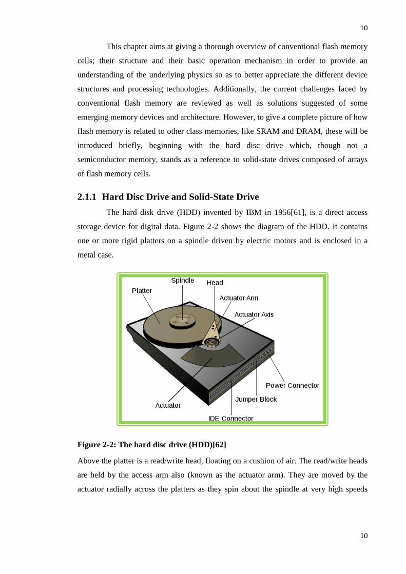
The hard disk drive (HDD) invented by IBM in 1956[61], is a direct access
storage device for digital data. Figure 2-2 shows the diagram of the HDD. It contains
one or more rigid platters on a spindle driven by electric motors and is enclosed in a
metal case.
Figure 2-2: The hard disc drive (HDD)[62]
Above the platter is a read/write head, floating on a cushion of air. The read/write heads
are held by the access arm also (known as the actuator arm). They are moved by the
actuator radially across the platters as they spin about the spindle at very high speeds

11
11
(4200 to 15000 rpm). The platters are made of nonmagnetic material usually aluminium
alloys or glass, which are coated with a very thin (10-20nm) layer of magnetic material,
e.g. cobalt-based alloys. The magnetic surfaces are divided into sub-micrometer regions
that are used to encode a single binary digit of information into each region. Each region
is composed of a few hundreds of magnetic grains and each grain about 10 nm in size
forms a magnetic domain. Each submicron region then forms a magnetic dipole which
generates a highly localized magnetic field nearby.
In a HDD, a write head is used to write data by directionally magnetizing a
ferromagnetic material to represent a binary digit 0 or 1. This is done by generating a
very strong local magnetic field. Data is read by detecting the magnetization of the
material. In today’s heads, the read and write elements are in close proximity, and made
of magneto-resistive and thin-film inductive materials respectively.
A solid-state drive (SSD) is a flash memory-based storage device. It is non-
volatile just like HDD, but unlike HDD, which is an electromechanical device with
moving parts (spinning disc and movable read/write heads), SSD contains no moving
parts and it uses NAND-based flash memory microchips. Early SSDs were RAM-based
16Kb introduced in 1978 by Texas Memory Systems that would have cost $1million per
Gb[63], but very recently very high density storage flash memory-based SSD of up to
256GB have been released, with lowest prices hitting $1.05 per Gb on a particular day
in June 2010[64]. That is a tremendous drop in price over the years. More consumers
are now turning away from HDD in preference of SDD for the following
advantages[65]:
1. They have premium input/output (I/O) performance for data access
operations over their HDD rivals, typically more than 100 times better;
2. They save power better than HDD; typically they use 0.51% of the power
HDDs would use for a given IOPS implementation. This is due to the fact
that they have no moving parts and they require fewer drives for the same
operation compared to HDDs;

12
12
3. The entire SDD is utilized for each intended purpose while the usable
capacity of HDD is significantly reduced to less than 50% by short-
stroking in order to increase the input/output performance per second
(IOPS);
4. Enterprise SSDs (savers and storage applications SDDs) occupy far less
space than HDDs;
5. Service life of SSD is longer (10years) than advertised service life of HDD
(5years). This is so because the moving parts of HDD wear out with time.
Despite these advantages, and the fact that SSD prices have dropped
tremendously, they are still more expensive than HDD for similar or equal capacity. For
instance, Higginbotham of priceG2 Inc reported that in mid 2010, the lowest price
tracked for a 2.5 inch internal portable 250GB HDD was $0.16/GB while the price was
$1.05/GB for 256GB SSD, showing SSD costs about 7 times HDD[64]. However, SSD
prices are dropping and it may be possible to get an 80GB SDD for approximately $23
by 2012[64]. With the advent of 3-D flash, situations may improve further.
2.1.2 Random Access Memory (RAM)
Random access memory (RAM) is a type of computer memory that allows
stored data to be accessed randomly regardless of its physical location. RAM is volatile-
information is only retained as long as the system is powered and lost once power is
turned off. RAM can be classed into two main types: Static RAM (SRAM) and
Dynamic RAM (DRAM). In DRAM, each bit of data is stored in a separate capacitor
which needs to be refreshed periodically in order not to lose the data. It is this refresh
requirement that makes it dynamic memory. On the other hand, SRAM does not require
the periodic refresh because it stores data in a bistable latching (flip-flop) circuitry, and
hence makes it faster than DRAM. A cell of DRAM is composed of one capacitor and
one transistor as shown in figure 2-3a. Conventionally though, a cell of SRAM has six
transistors as shown in figure 2-3b[66]. M5 and M6 are access transistors, M1-M4 form
the cross coupled inverters in the flip-flop circuit powered by a constant voltage Vdd.

13
13
The simple structure of DRAM gives it its advantage over SRAM because high
densities can be reached with DRAM which is not possible with SRAM. The
disadvantage of DRAM over SRAM is that it is slower and the requirement of refresh
makes its power consumption significantly more.
Figure 2-3: Illustration of (a) DRAM and (b) SRAM[66]
2.1.3 Read Only Memory (ROM)
ROM refers to read only memory. This is computer storage device in which
data stored cannot be easily modified. Unlike RAM, it is non-volatile. Different types of
ROM exist; these are Programmable Read Only Memory (PROM), Erasable
Programmable ROM (EPROM) and Electrically Erasable Programmable ROM
(EEPROM). PROM allows the user to programme it once by physically altering its
structure through the application of a high voltage pulse after its initial programmed
state. EPROM on the other hand can be erased or repeatedly reset to its unprogrammed
state by exposure to UV-radiation. EEPROM is user-modifiable, read-only memory
(ROM) that can be erased and reprogrammed repeatedly through the application of
higher than normal electrical voltage generated externally (or internally in the case of
modern EEPROMs). Thus, it is electrically-erasable unlike EPROMs that are UV-
erasable. Furthermore, programming of EPROM is by hot electron injection while
EEPROMs are programmed and erased by a field electron emission method known as

14
14
Fowler-Nordheim tunnelling. These programming techniques will be dealt with in
greater details in subsequent sections. Because of the erase method of EPROMs, they
need to be encapsulated with a material that is not permeable to UV radiation.
Both EPROM and EEPROM have the floating gate transistor structure that will
also be detailed in subsequent sections. The floating gate transistor has a Polycrystalline
silicon gate which is isolated and surrounded completely by a good quality insulating
material, usually silicon dioxide. During a write operation, electrons are put onto the
floating gate either by channel hot electron injection or by Fowler-Nordheim tunnelling
and erased by UV or by FN. The stored electrons are prevented from leaking out by the
insulator when power is turned off. This is what makes these devices non-volatile.
Failure of these devices can occur through repeated write/erase cycles. During rewrites,
the gate oxide layer of the floating gate traps some electrons. These generate an electric
field which adds to that of electrons in the floating gate, thus lowering the threshold
voltage shift between the programmed and erased states of the transistor. After a
number of rewrites, the threshold voltage shift between the write and erased states
becomes insignificant to be able to distinguish between the states and thus endurance
failure occurs. Manufacturers usually specify 104-10
6 write/erase cycles as device
endurance[67]. Apart from this write endurance failure, stored charge in the floating
gate can also leak through the gate oxides especially at high temperatures thus reverting
the device to an erased state. A minimum of 10 years retention time is usually specified
by manufacturers[67].
2.1.4 Non-Volatile RAM
This is a class of random accessed memories which retain stored data even
when not powered. Flash memory falls within this class of memory. Flash memory is
basically identical to the EEPROM but differs in its internal layout. Depending on the
way the cells are wired in flash memory, we can obtain the NOR-flash and NAND as
shown in figure 4. In the case where each cell has one end connected to ground and the
other to the bit line, a NOR is obtained (figure 2-4a). It is called NOR because it
basically functions like a NOR gate- when a word line is high, a corresponding
transistor acts to bring the output bit line to low. For NAND flash, several transistors are
connected in series (figure 2-4b). In this type of flash, the output bit line is low if only

15
15
all the input word lines are pulled high above a certain threshold voltage of the
transistors, an action identical to the NAND gate. NAND and NOR also differ in their
programming; while NOR-flash is written by hot electron injection and erased by
quantum tunnelling, NAND is written and erased by tunnelling injection and tunnelling
release respectively.
Figure 2-4: Cell connections in (a) NOR flash and (b) NAND flash memory devices
2.2 Brief Historical Evolution of Floating Gate Non-Volatile
Memory
D. Kahng and S. M. Sze in 1967 first suggested the floating gate non-volatile
memory (FG NVM) device[68]. Their proposed device was a basic MOS structure with
the gate structure replaced by an extremely thin tunnel oxide necessary to obtain an
extremely high electric field for electron tunnelling to a metal FG for capturing and
storing of electrons. Above the metal FG is another oxide layer thick enough to prevent
electron leakage to an external metal gate as shown in figure 2-5. The structure thus
obtained was a metal-insulator-metal-insulator-semiconductor (MIMIS) cell. In the
Kahng and Sze device, programming and erasure of the cell is by direct tunnelling.
Applying a positive voltage to the external metal gate causes electrons to tunnel directly
through the thin oxide layer onto the metal FG. When the gate voltage is removed,

16
16
electrons remain trapped in the isolated metal FG as the field in the tunnel oxide is too
small to permit back-tunnelling. Applying a negative voltage to the external metal gate
leads to erasure (electron discharge) of the FG by the same direct tunnelling mechanism.
This MIMIS device is historically important in that it introduced the basic
concept of NVM devices and contained concepts that led to the development of the
direct tunnelling concept used in charge trapping devices and the FG concept in various
FG memory types. However, some technological constraints served as stringent
deterrents for this device; the difficulty in achieving extremely thin defect-free tunnel
oxides less than 5nm at that time, a requirement imposed by the direct tunnelling
mechanism. Furthermore any pinhole on the tunnel dielectric would cause the complete
erasure of electrons from the metal FG.
Later in 1967, the metal-nitride-oxide-semiconductor (MNOS) cell (figure 2-
6a) was introduced by Wegener et. al.[69]. This was a solution to one of the problems
with the MIMIS cell. In this cell, a nitride layer replaced the metal FG and control gate
oxide. The nitride layer contains trapping centres of holes and electrons and fulfils the
storage function of the metal FG in a MIMIS cell. The individual traps are discrete
(isolated from each other) and thus in the situation where there is a pinhole in the tunnel
oxide, the cell is not completely discharged (erased) as in MIMIS. The application of a
high voltage to the gate causes electrons to tunnel from the silicon conduction band to
the nitride conduction band and eventually gets trapped in nitride traps. This leads to a
Figure 2-5: metal-insulator-metal-insulator-semiconductor (MIMIS) FG device.

17
17
positive threshold voltage shift. A high negative voltage applied to the gate causes holes
to tunnel from the silicon valence band to the nitride valence band leading to a negative
threshold voltage shift. This electrical programming and erasing concept is applied in
several kinds of applications specifically in EEPROMs. This class of memory device is
mostly used in military and applications that are resistant to radiation.
In 1971, Frohman-Bentchkowsky introduced the very first operational FG
device known as the FG avalanche injection MOS (FAMOS)[70-72]. The FG in this
cell was made of Polycrystalline silicon surrounded by a thick (≈ 100nm) oxide layer
(figure 2-6b). With the FAMOS cell, the inherent problem of very thin tunnel oxide in
MIMIS was solved and the shorting path was obviated. However, the programme and
erase mechanisms were different; (not the direct tunnelling in MIMIS.) programming in
FAMOS is by applying a very high negative voltage (≥ 30V) at the drain to cause the
injection of highly energetic electrons from avalanche plasma in the drain region
beneath the gate. This avalanche of electrons is created by the high negative voltage.
These injected energetic electrons drift towards the FG by the help of the positive field
in the oxide induced by capacitive coupling between the FG and the drain [72].
Figure 2-6: Diagrammatic representation of (a) The MNOS cell, (b) the
FAMOS cell and (c) the SAMOS cell.
18
18
A disadvantage of this device was the inefficiency of the write process.
Electrical erasure did not exist since no field emission was possible due to lack of an
external gate. Erasure of this memory cell type was either by UV or X-ray irradiation.
These drawbacks were later alleviated by several adopted concepts among which was
the Staked gate Avalanche injection MOS (SAMOS) introduced by H. Iizuka et al in
1972[73].
The SAMOS shown in figure 2-6c above differed from FAMOS in that it had
an external gate added to its structure. This new structure improved the writing
efficiency and programming speed by the increase in electron drift velocity in the oxide,
a field induced energy barrier lowering at the Si/SiO2 interface and a decreased drain
breakdown voltage[74]. Field emission at the top dielectric as a result of the polyoxide
conduction also made the device to be electrical erasable. Electrically erasable
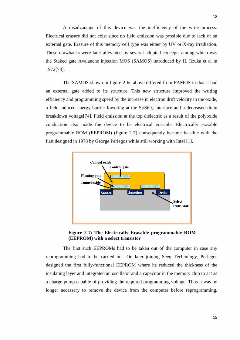
programmable ROM (EEPROM) (figure 2-7) consequently became feasible with the
first designed in 1978 by George Perlegos while still working with Intel [1].
The first such EEPROMs had to be taken out of the computer in case any
reprogramming had to be carried out. On later joining Seeq Technology, Perlegos
designed the first fully-functional EEPROM where he reduced the thickness of the
insulating layer and integrated an oscillator and a capacitor in the memory chip to act as
a charge pump capable of providing the required programming voltage. Thus it was no
longer necessary to remove the device from the computer before reprogramming.
Figure 2-7: The Electrically Erasable programmable ROM
(EEPROM) with a select transistor
19
19
EEPROMs though reprogrammable, could be altered only in a finite number of times,
which is why they were mostly used in storing only configuration data such as the
computer basic input/output system (BIOS) code, which does not require frequent
reprogramming.
In the 1980s, EEPROM evolved to flash memory through Toshiba’s F.
Masuoka invention [75]. Flash memory is identical to EEPROM but they differ in the
mode of data erasure from the FG. Though introduced in the mid 80s, the flash memory
market did not take off until the technology was proven to be reliable and
manufacturable[76]. In flash, data is erased in blocks and not bitwise as in EEPROM.
Flash has since grown to become the largest market in non-volatile memory, due to the
highly competitive trade-off between functionality and cost per bit. Novel applications
of flash have also arisen such as in solid-state drives (SSD)[77] mentioned above for
portable computers and smart cards. Early devices were programmed by hot electron
injection, but novel device structures have been proposed that use Fowler-Nordheim
tunnelling for both programme and erase. Others using the source-side injection
programming mechanism have gained interest because of their unique combination of
fast programming capabilities with low power consumption.
In 1980, there was an important breakthrough for MNOS with the development
of a silicon-gate n-channel silicon-nitride-oxide-semiconductor (SNOS) process that
resulted in the first 16Kbit SNOS EEPROM [78]. This SNOS EEPROM cell consists of
two transistors; a MOS select transistor and the SNOS storage transistor made up of a
20-40nm nitride layer above the ultra-thin oxide on silicon channel. The nitride has
discrete traps wherein net positive and negative charges can be stored[79]. During a
write process, electrons are injected into the silicon nitride conduction band by the
modified Fowler-Nordheim tunnelling[80] through the application of a high positive
voltage at the gate with the well grounded. In order to erase the cell, a high positive
voltage is applied to the well while the gate is grounded. This leads to direct tunnelling
of holes from the silicon valence band into the nitride valence band or traps. The cell is
read by addressing it through the select transistor and sensing the state of the SNOS
transistor [79, 81]. The ultra-thin oxide leaves the possibility of back-tunnelling to occur
thereby modifying the charge in the silicon nitride even when the gate is grounded.

20
20
When a thin oxide layer is added on top of the nitride, the so called silicon-
oxide-nitride-oxide-semiconductor (SONOS) device is obtained in which charge
injection from the gate is reduced. This device was first reported by P. C. Chen[82] in
1977 and further improvements in the structure with regards to layer thicknesses of the
oxides and nitride done by various researchers[83-88]. The cell is programmed by
applying a required positive voltage (7V) on the Polycrystalline silicon gate. This
causes electrons to tunnel from the substrate to the charge storage layer of the ONO
stack by Fowler-Nordheim tunnelling. The device is erased by applying the same
voltage of opposite polarity which causes Fowler-Nordheim tunnelling of holes from
the substrate to the charge traps in the storage layer.
2.3 Flash Memory Overview
As the aforementioned flash memory invented by Masuoka et al[75] is a non-
volatile electrically re-writable class of memory devices, it can store data for a very long
time even when unpowered. It is a particular type of EEPROM that is erased and
programmed in large blocks unlike EEPROMs that are electrically erasable and
programmed per byte. It is called flash because many stored blocks (large number of
cells) can be erased (flashed) at once. It costs far less than byte-programmable
EEPROM and therefore has become the dominant NVM technology.
Figure 2-8: Cell structure of the (a) Silicon-Nitride-Oxide-Semiconductor
(SNOS) and (b) Silicon-Oxide-Nitride-Oxide-Semiconductor (SONOS) devices.
The MOS select transistor is not shown.

21
21
Two major applications of flash include NVM integration in logic systems
where they, among other uses, allow software updates, store identification codes and
reconfigure the system on the field. The other major application is to create storing
elements like solid-state disks (SSD) made of memory arrays configured to create large
size memories to compete with miniaturized hard disks. This application is very
attractive to portable devices since SSDs have small dimensions, low power
consumption and no mobile parts making them more robust. In computer programme
management, programmes can be stored in flash chips without being continuously
loaded and unloaded from the HDD. Flash technology has advanced to a great extent
and today it stands as a strong challenger and competitor to other non-volatile
memories.
2.3.1 Flash Memory Cell Structure
The conventional commercial flash elementary cell is a MOSFET with a
continuous Polycrystalline silicon FG, as shown in figure 2-9. The FG is coupled to the
control gate by a control oxide also known as interpoly dielectric (IPD) and to the
silicon channel by a thin tunnel oxide (≤ 10nm) usually silicon dioxide. The gate is
called “floating” because it is completely electrically isolated from the channel and top
gate by the tunnel and control dielectrics respectively. The control gate acts as the
external gate of the MOSFET in figure 2-9a. The IPD can also be a nitride or stacked
layers of oxides and nitrides (oxide-nitride-oxide) ONO. The source and drain regions
are highly-doped regions of the substrate that act as the terminals for electron flow. The
silicon substrate acts as a channel for electrons from source to drain. The FG stores
charge and thus acts like a potential well. Once charge is stored in it, it cannot move
unless an external force is applied. The charge is prevented from moving by the
dielectrics surrounding the FG. Moving charge into the FG can be achieved by applying
a high field to both the control gate and the drain such that the MOSFET is in
saturation. To remove the charge, a high positive voltage is applied to the source and the
control gate grounded. Putting and removing charge from the FG causes the MOSFET
to have two different threshold voltages corresponding to two logic levels 0 and 1.
When there is charge in the FG, the MOSFET is in logic level “0” and when charge is

22
22
removed it is in logic state “1”. These two states form the basis of the flash memory
device.
2.3.2 The Capacitor Model and Equations of the FG MOS Device
In order to understand the electrical behaviour of the FG device, use is made of
the simple model by S.T. Wang[89] shown in figure 2-10. CFC, CFS, CFB and CFD are the
capacitances between the FG and the control gate, source, base and drain respectively
while VCG, VS, VD and VB are the potentials of the control gate, source, drain and bulk
respectively and VFG is the potential on the FG.
Figure 2-9: The basic cell structure of (a) the MOSFET and (b) the FG flash
memory cell.
Figure 2-10: Illustration of the capacitance model of the
FG memory cell.

23
23
The total capacitance Ctot of the FG MOS device is Ctot=CFC+CFS+CFB+CFD[89]. If the
FG coupling ratio to the other electrodes is defined as κelectrode = CF-electrode/Ctot, (e.g. κd=
CFD/Ctot), then in the case where no charge is stored in the FG, Q=0. This means that
0)()()()( DFGFDBFGFBsFGFSCGFGFC CCCCCCVVCCCC (2-1)
From eqn. (2-1), the FG potential can thus be determined from
DSdBbssGSgFG VVVVV (2-2)
where the potentials are with respect to the source and κg, κs, κb, and κd are the FG
coupling ratios to the control gate, source, base and drain respectively. In the case where
the source and bulk are grounded, i.e. VS and VB both equal to zero, eqn. (2-2) reduces
to
)( DSGSgDSdGSgFG fVVVVV (2-3)
where FCFDgd CCf // the capacitive coupling ratio between the FG and drain
to FG and control gate.
If charge is stored in the FG, i.e. Q 0, eqn. (2-3) modifies to
tot
DSGSg
tot
DSdGSgFGC
QfVV
C
QVVV )(
(2-4)
In order to compare these equations with those of the MOS transistor, the MOS
gate potential must be replaced by the FG potential, and transforming parameters such
as threshold voltage Vt and conductivity factor β, to values measured with respect to the
control gate. The threshold voltage of the MOS transistor is given by[90]
ox
tC
QKV (2-5)
where K is a constant that depends on the gate and substrate material, doping and gate
oxide thickness, Q is the charge weighted with respect to its position in the gate oxide
and Cox is the oxide capacitance. From (2-2), redefining VtFG
= κgVtCG
for VDS = 0 and
24
24
βFG
= βCG
/κg[89] makes it easier to deduce the I-V relationship of the FG MOS that can
be compared to the conventional MOS transistors in the linear (triode) (TR) and
saturation regions (SR) respectively. TR is the region in the IDS-VDS characteristic
where the current increases rapidly with increase in VDS while SR is the region where
IDS saturates as VDS increases for a MOS transistor. In the TR, for the MOS transistor,
},2
){(2
DS
DStGSDS
VVVVI valid for tGSDS VVV (2-6a)
For the FG MOS transistor, these transform to
},)2
1(){( 2
DS
g
DStGSDS VfVVVI valid for tDSGSgDS VfVVV (2-6b)In
the saturation regime (SR), the MOS transistor gives
2)(2
tGSDS VVI , valid for tGSDS VVV
(2-7a)
For the FG transistor, this transforms to
,)(2
2
tDSGS
g
DS VfVVI valid for tDSGSgDS VfVVV (2-7b)
From equation (2-4) when Q 0,
FC
FG
t
ggtot
FG
t
g
CG
tC
QV
C
QVV
11
(2-8)
})2
1())
11({( 2
DS
g
DS
totg
tGSDS VfVC
QVVI
(2-9)
From equation (2-8), it can be observed that the threshold voltage VtCG
written as Vt, is
dependent on charge Q stored in the device. The threshold voltage shift when charge is
stored in the device is
FC
ttC
QVVV 0 (2-10)

25
25
where Vto is the threshold voltage when no charge is stored. From equation (2-9), it can
also be observed that when charge is stored in the device, it causes a shift in the I-V
characteristics of the device. This shift in threshold voltage of the IDS vs. VGS is
otherwise known as the memory window. The presence of charge in the FG thus affects
the current level to sense the memory state. Figure 2-11 is an illustration of the I-V
characteristic of the FG MOS showing the two states of the device, charged and
uncharged.
Other deductions can be made from equations (2-6) and (2-7) regarding the
differences in the I-V behaviour of the conventional MOS and the FG MOS transistors.
These differences are primarily due to the capacitive coupling between the drain and the
FG. The first observation is that for the FG and conventional MOS transistor, the
boundary between TR and SR are given respectively by
tDSGSgDS VfVVV and tGSDS VVV (2-11)
From equation (2-6) it is observed that the FG transistor can go into depletion-mode
operation and can conduct current even when |VGS| < |Vt| because of the “drain turn-on”
effect wherein the channel is turned on by the drain voltage through the term fVDS.
Furthermore, saturation does not occur in the FG transistor as IDS continues to increase
Figure 2-11: I-V characteristics of the FG MOS device at the neutral "1"
and charged "0" states. The threshold voltage shift ∆Vt is proportional to
the charge stored in the FG. ∆Vt is also known as the memory window.
26
26
with increase in VDS. This contrasts with the MOS transistor where SR is essentially
where IDS is independent of VDS (equation (2-7)). Furthermore in the SR regime for the
FG transistor, the transconductance which is the partial differential of the drain current
with respect to the gate voltage at constant drain voltage is expressed as in equation (2-
12) increases with VDS unlike in the MOS where it is independent of VDS.
)(tan tDSGSgtconsV
GS
DS VfVVV
IG
DS (2-12)
The capacitive coupling ratio f depends only on CD and CFC and its value can be
obtained or verified by
tconsI
DS
GS
DSV
Vf tan (2-13)
2.3.3 Working Mechanisms of Flash Memory Cell
The conventional floating gate memory cell operation mechanisms basically
involve charge injection into and removal from the FG, thereby programming the
MOSFET to two different threshold voltages corresponding to two logic levels. When
electrons are stored in the FG, the cell is said to be programmed and exhibit a high
threshold voltage state. It is assigned to logic level “0” as shown in figure 2-11. On the
other hand, when electrons are removed from the FG, the cell exhibits a low threshold
voltage and is said to be erased. It is assigned the logic level “1” also shown in figure 2-
11. In a read operation, a moderate voltage is applied between the drain and the control
gate. This causes the capacitively coupled FG voltage to be between the high and low
threshold voltages of the programmed cell.
Different mechanisms of charge transfer into and from the FG have been
proposed, all involving charge passage to the FG through a thin layer of dielectric
material for both the erase and write operations. Two main mechanisms are
predominant for the programme and erase operations; channel hot electron (CHE)
injection and Fowler-Nordheim (FN) tunnelling. CHE injection and FN tunnelling are
used for writing to- and erasing from the FG respectively of a NOR flash memory. For
NAND flash, programme and erase are both by FN tunnelling mechanism.
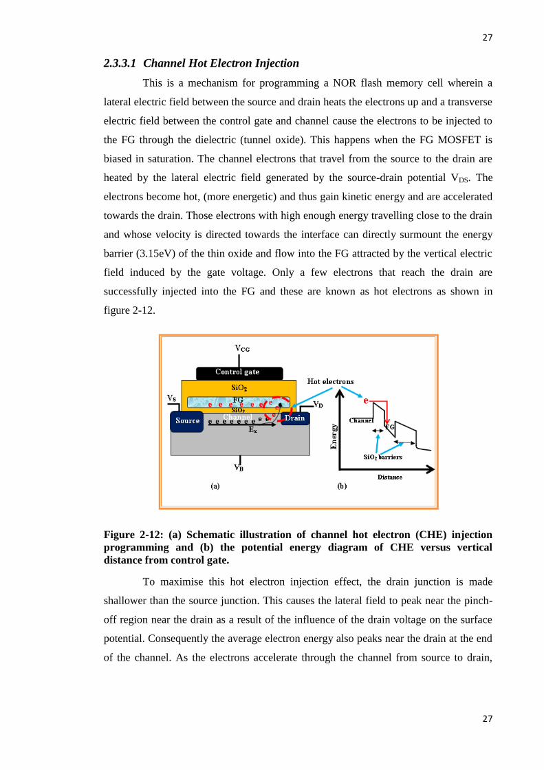
27
27
2.3.3.1 Channel Hot Electron Injection
This is a mechanism for programming a NOR flash memory cell wherein a
lateral electric field between the source and drain heats the electrons up and a transverse
electric field between the control gate and channel cause the electrons to be injected to
the FG through the dielectric (tunnel oxide). This happens when the FG MOSFET is
biased in saturation. The channel electrons that travel from the source to the drain are
heated by the lateral electric field generated by the source-drain potential VDS. The
electrons become hot, (more energetic) and thus gain kinetic energy and are accelerated
towards the drain. Those electrons with high enough energy travelling close to the drain
and whose velocity is directed towards the interface can directly surmount the energy
barrier (3.15eV) of the thin oxide and flow into the FG attracted by the vertical electric
field induced by the gate voltage. Only a few electrons that reach the drain are
successfully injected into the FG and these are known as hot electrons as shown in
figure 2-12.
Figure 2-12: (a) Schematic illustration of channel hot electron (CHE) injection
programming and (b) the potential energy diagram of CHE versus vertical
distance from control gate.
To maximise this hot electron injection effect, the drain junction is made
shallower than the source junction. This causes the lateral field to peak near the pinch-
off region near the drain as a result of the influence of the drain voltage on the surface
potential. Consequently the average electron energy also peaks near the drain at the end
of the channel. As the electrons accelerate through the channel from source to drain,
28
28
they generate electron-hole pairs through impact ionization. These generated electrons
(holes) are known as secondary electrons (secondary holes). The secondary holes are
eventually collected by the base contact thus giving rise to the base current IB [91, 92].
Meanwhile, the secondary electrons can gain enough kinetic energy to be injected into
the gate consequently contributing to the gate current IG. Thus the gate and base
currents have the same origin, being the accelerating hot electrons as they travel along
the channel.
A number of factors affect the efficiency of this charging (programming)
method. These are the lateral electric field between the source and drain which is
responsible for heating up and accelerating the electrons toward the drain, and the
vertical electric field close to the drain. This vertical field influences the probability for
the hot electrons to tunnel through the potential barrier to the FG. As mentioned earlier,
very few electrons actually cross the potential barrier and reach the FG. An effective
evaluation of the number of hot electrons would require knowledge of the energy
distribution as a function of lateral field, the momentum distribution as a function of
electron energy, the shape and height of the potential barrier and the probability that an
electron with a certain amount of energy and wave vector a distance d from the Si/SiO2
interface will surmount the barrier. A quantitative model would be very complex to
study, as each of these factors has to be specified at each point of the channel. However,
the lucky electron model developed by Hu[93] and the hot electron injection current
model[94] are often employed to qualitatively study the efficiency of this FG
programming method.
The lucky electron model is based on the probability that an electron would be
lucky to travel across the channel a distance several times the mean free path without
scattering and eventually acquire enough kinetic energy to surmount the barrier if a
collision pushes it towards the Si/SiO2 interface. Denoting the potential barrier by Φo
and assuming the lateral electric field Ex (as in figure 2-12) to be constant, then the hot
electron needs to travel a distance d = Φo/Ex to acquire enough kinetic energy (Φo=3.15
eV) to overcome the barrier. However, it has to do this distance d without suffering any
collision and the probability of doing so is given by[95] ℮-d/λ
= ℮(-Φo/Exλ)
where λ is the
mean free path associated with phonon scattering dependent both on the optical-phonon

29
29
mean free path and the impact-ionization mean free path. Its value at room temperature
is ≈ 91Å[96]. The probability of an electron acquiring enough kinetic energy to cross
the barrier and having enough normal momentum after redirection is given by[93]
)exp(4
0
00
x
x
E
EP (2-14).
The hot electron injection current can thus be expressed as [94]
)exp(4
0
2
0 x
xDSdCHE
E
EIAI (2-15)
where Ad is a fitting parameter (constant). It can be observed from equation (2-15) that
the injected current increases exponentially with a decrease in the barrier height.
2.3.3.2 Fowler-Nordheim Tunnelling
Fowler-Nordheim (FN) tunnelling is used for programming NAND flash
and for erasing NOR and NAND. FN is a quantum mechanical field emission
process[97] in which electrons tunnel through a barrier in the presence of a high electric
field. Applying a high electric field across a polycrystalline silicon-SiO2-silicon
structure modifies its energy band structure. The high field causes electrons in the
silicon conduction band to see a triangular energy barrier whose width depends on the
applied field and height on the electrode material and the band structure of the silicon
dioxide. At sufficiently high electric fields, the width of the barrier becomes so small
that the electrons in the silicon conduction band can tunnel through the silicon dioxide
into the floating gate. Under erase conditions, a large negative potential is applied on the
control gate that sets up a strong electric field between the gate and the source. This
field reduces the energy barrier width and increases the energy barrier slope thus
effectively thinning down the top of the barrier making it triangular. Concurrently, this
high field also imparts kinetic energy to some of the electrons in the FG thus setting
these to move energetically towards the top of the tunnel oxide potential barrier where
they effectively penetrate in a wave-like manner through the reduced barrier to the
source. These electrons then rapidly thermalize through interaction with the lattice and
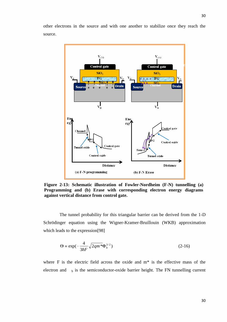
30
30
other electrons in the source and with one another to stabilize once they reach the
source.
The tunnel probability for this triangular barrier can be derived from the 1-D
Schrödinger equation using the Wigner-Kramer-Bruillouin (WKB) approximation
which leads to the expression[98]
)*23
4exp( 2/3
bqmF
(2-16)
where F is the electric field across the oxide and m* is the effective mass of the
electron and b is the semiconductor-oxide barrier height. The FN tunnelling current
Contr
ol gate
Figure 2-13: Schematic illustration of Fowler-Nordheim (F-N) tunnelling (a)
Programming and (b) Erase with corresponding electron energy diagrams
against vertical distance from control gate.

31
31
density J, can be obtained from the product of the number n, of electrons arriving at the
Si/SiO2 interface per unit area and time, the velocity VR with which these electrons
arrive the Si/SiO2 interface and the tunnelling probability. That velocity is known as the
Richardson velocity. Thus current density J is given by
)*23
4exp( 2/32
bR qmF
FnqVJ
(2-17)
where )16/( 23
bq and b is as defined above [97-99]
2.3.3.3 Reading Operation
The presence of charge in the FG greatly influences the current level used to
sense the cell and as shown in equation (2-10), the threshold voltage shift is directly
proportional to the amount of charge stored in the cell. Therefore, defining a proper
charge and a corresponding voltage shift, a reading voltage can possibly be fixed such
that the current of the “1” state corresponding to uncharged state is very high and that of
the “0” state corresponding to the charged state is low (zero current reading). As shown
in figure 2-11, when the gate voltage is VR, a high current is sensed at the “1”-state and
zero current is sensed at “0”-state. We can thus define the logic states “0” as a state at
which charge is stored in the FG and zero current is sensed and the “1” state as a state at
which no charge is stored in the FG and a high current is sensed.
2.3.4 Reliability
Two important functional characteristics of flash memory used to evaluate the
performance of the device and which are the main reliability concerns are data retention
and write/erase cycle endurance [7, 100, 101]. A study carried out by P. Muroke[102]
has identified early failure rate of flash memory devices due to latent defects as the
main cause of field failure. As device cell sizes continue to scale down, challenges
related to high electric fields and smaller thicknesses of gate oxides and IPD are certain
to make these defect related early failure rates worse[12]. Knowledge of the
fundamentals of the failure mechanisms associated with the tunnel oxide and the IPD
would thus lead to a better understanding of retention and write/erase cycle endurance
characteristics as the two oxide layers affect these characteristics.
32
32
Tunnel oxide breakdown and the trapping of electrons in the oxide due to high
electric field stressing during CHE injection or F-N programme and erase operations are
the primary failure mechanisms of tunnel (gate) oxide. Oxide breakdown occurs after a
fixed amount of charge per unit area has been injected. This fixed amount of charge per
unit area is a function of electric field[103] and the higher the amount, the better the
quality of the oxide. This fixed charge per unit area injected through the oxide also
depends on the thickness, the mode of current injection and operation temperature
[103]. Trapped electrons (charges) in the oxide during injection can be attributed to
defects in the oxide as well as broken Si-O bonds. These trapped charges in the oxide
layers thus affect the injection field and thus the amount of charge transferred to or from
the FG during programming and erase operations.
The FG is isolated from the top (control) gate, source and drain by the control
oxide or IPD. Thus the IPD prevents charge leakage to other electrodes and should
therefore be defect-free to perfectly function as such. However, the surface topology of
the Polycrystalline silicon FG is often modified through enhanced oxidation of the
Polycrystalline silicon at grain boundaries during the IPD growth[104], forming
protrusions and inclusions and thus leading to surface non-uniformity. This causes the
electric field to differ substantially[105] thus resulting in higher leakage currents. Other
factors responsible for the quality of the IPD are the doping of the source/drain regions
and the deposition temperatures of the Polycrystalline silicon and the oxidation
temperature which may affect the materials at the interfaces differently and cause
migration of dopants away from desired locations [105, 106]. ONO multilayer are now
commonly preferred to the single SiO2 layer as IPD because the oxide-nitride-oxide
(ONO) stack registers lower defect densities and can withstand higher electric fields.
The low leakage currents for this stack is simply due to the fact that leaked charges from
the FG get trapped in the oxide-nitride interface, build up and thus repel further electron
leakage from the FG[107]. Typical thicknesses in the ONO stack are 5-10nm, 20nm and
3nm for the bottom oxide, nitride and top oxide respectively.
2.3.4.1 Write/Erase Cycle Endurance
Endurance can simply be defined as the resistance to failure of the flash
memory device after repeated programme/erase (P/E) cycles. Thus the endurance
33
33
characteristic is the memory window (threshold voltage) as a function of the number of
P/E cycles, which usually shows memory window closure after a high number of P/E
cycles. Flash memories are typically specified to endure 104-10
6P/E cycles [108-111].
The phenomenon of window closure occurs when the threshold voltages of the
programmed and erased states cannot be distinguished from each other. Repeated P/E
cycles is known to induce stress in the tunnel oxide which causes its degradation and
leads to the phenomenon known as stress-induced leakage currents (SILC)[112]. P/E
cycling leads to tunnel oxide breakdown and trap-ups (charge traps) during the CHE
injection or F-N operations. These are damaging to memory devices and limit their
number of P/E cycles. SILC can be attributed to stress–induced oxide defects as well as
trap-assisted tunnelling mechanism and are controlled by the stress field, the amount of
charge injected during the stress and the oxide thickness. For a given stress level, the
thinner the oxide layer, the stronger the leakage current [113-115].
2.3.4.2 Retention
Flash memory retention can be defined as the ability of a memory bit to retain
its stored data over a long period of time whether powered or unpowered. Thus when a
memory cell can no longer retain charge in its FG, its retention capabilities are said to
be affected. The usually-specified retention time for flash memory by industry is 10
years [111, 116]. There are different avenues through which charge can leak away from
the FG. These include [7]
1. charge loss through defects in the tunnel oxide;
2. charge loss through defects in the IPD;
3. detrapping of charge from insulating layers surrounding the FG and
4. mobile ion contamination
Defects in the tunnel oxide can be due to defects in the device structure or due
to the physical mechanisms used in programming and erasing the cell. These losses of
charge or charge variation in the FG usually lead to a variation in the FG potential and
consequently to a shift in the threshold voltage of the memory cell. Thus it is possible to

34
34
quantify retention by estimating the time it takes for the FG to discharge when it
intended to keep the data stored. From equation (2-10),
tFGFG dVCdQ (2-18)
where dQFG, CFG and dVt are the charge lost from the FG, the FG capacitance and the
threshold voltage shifts respectively. From equation (2-18), the number of electrons lost
from the FG can be associated to the leakage current Il as[117]
191919 106.1106.1106.1 x
dVC
x
dtI
x
dQdn tFGlFG (2-19)
where 1.6 x 10⁻¹⁹
C is the charge of an electron. Thus knowing the threshold voltage
shift, it is possible to estimate the retention time for some measured leakage current for
a typical FG capacitance of the order of 10-15
F, about 104-10
5 electrons are lost from
the FG for a threshold voltage shift of about 2V.
2.3.4.3 Cell Disturb
Cell disturb is a failure mechanism in flash memories that concerns data
corruption of an unselected written cell caused by programming or reading some
selected cells[118]. The failure mechanism is known as programme disturb when
programming and read disturb when reading of selected cells cause data corruption in
the unselected. Programme disturbs are more frequently observed because of the
relatively high voltages applied to the selected cells for programming.
Two types of programme disturbs are common: row disturb or gate stress and
column disturb or drain stress. Row disturbs occur due to gate stress when programming
other cells in the same wordline while column disturb occurs due to drain stress applied
to a cell while programming other cells in the same bitline. Applying a high voltage to a
selected row (gate) during programming means that all the cells in that row must
withstand that stress without losing data. Data loss in this disturb can either be by a
leakage in the gate (tunnel) oxide or by a leakage in the control oxide (IPD). On the
other hand, under column disturb or drain stress, data can be lost from programmed
cells by F-N tunnelling from the FG to the drain. This is also known as soft erasing.

35
35
Other cell disturbs are dc erase and dc programme[100]. DC programme occurs on cells
that are in erased states on the same wordline as the cell being programmed. When the
wordline is raised to a high voltage, the electric field across the tunnel oxide may be
high enough to cause electrons to tunnel into the FG from the substrate thus increasing
the threshold voltage of the cell. In severe cases, the cell in unintentionally programmed
and this is known as soft write. This for instance can happen in cell (R2, C1) if it is in
the erased state and cell (R2, C2) is being programmed as shown in figure 2-14. DC
erase occurs on already programmed cells in the same wordline as the cell being
programmed. A high programming voltage may cause a high electric field across the
IPD (control oxide) of the programmed cell which may be capable of causing
conduction of electrons across it from the FG to the control gate. This is also known as
Polycrystalline silicon to Polycrystalline silicon erase and in severe cases may cause
complete loss of data. If cell (R2, C3) were initially programmed before the shaded cell
is programmed as in figure 2-14, dc erase could likely occur there. Disturb propagations
can be prevented by using block select transistors in a divided bitline and wordline
organization to completely isolate each sector.
Figure 2-14: An illustration of cell disturbs in an array of flash memory cells.
The shaded cell is being programmed while cell disturb occurs in the other
cells in the same wordline (row) and bitline (column).
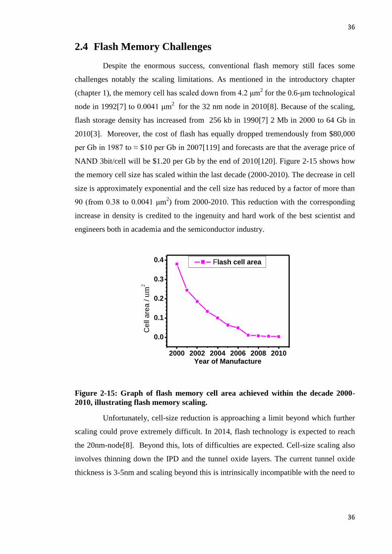
36
36
2.4 Flash Memory Challenges
Despite the enormous success, conventional flash memory still faces some
challenges notably the scaling limitations. As mentioned in the introductory chapter
(chapter 1), the memory cell has scaled down from 4.2 μm2 for the 0.6-μm technological
node in 1992[7] to 0.0041 μm2
for the 32 nm node in 2010[8]. Because of the scaling,
flash storage density has increased from 256 kb in 1990[7] 2 Mb in 2000 to 64 Gb in
2010[3]. Moreover, the cost of flash has equally dropped tremendously from $80,000
per Gb in 1987 to ≈ $10 per Gb in 2007[119] and forecasts are that the average price of
NAND 3bit/cell will be $1.20 per Gb by the end of 2010[120]. Figure 2-15 shows how
the memory cell size has scaled within the last decade (2000-2010). The decrease in cell
size is approximately exponential and the cell size has reduced by a factor of more than
90 (from 0.38 to 0.0041 μm2) from 2000-2010. This reduction with the corresponding
increase in density is credited to the ingenuity and hard work of the best scientist and
engineers both in academia and the semiconductor industry.
2000 2002 2004 2006 2008 2010
0.0
0.1
0.2
0.3
0.4
Ce
ll a
rea
/ u
m2
Year of Manufacture
Flash cell area
Figure 2-15: Graph of flash memory cell area achieved within the decade 2000-
2010, illustrating flash memory scaling.
Unfortunately, cell-size reduction is approaching a limit beyond which further
scaling could prove extremely difficult. In 2014, flash technology is expected to reach
the 20nm-node[8]. Beyond this, lots of difficulties are expected. Cell-size scaling also
involves thinning down the IPD and the tunnel oxide layers. The current tunnel oxide
thickness is 3-5nm and scaling beyond this is intrinsically incompatible with the need to
37
37
preserve the minimum thickness in these devices to maintain the reliability and data
retention after many write/erase cycles[121]. Atwood G[12] and Lai S. K[119] have
grouped these scaling limitations into three main classes, namely: physical scaling
defined by lithography; electrical scaling defined by program/erase voltages and
reliability scaling defined by the fundamental physics of the program, erase and storage
mechanisms. These classes however do not have a strict line of demarcation between
them as one is intrinsically linked to another. For instance, reduction of channel length
concerns lithography and thus physical scaling but an understanding of the effects
caused by channel length reduction is related to the effects of the voltages required for
CHE injection programming, which is more to do with electrical scaling.
Concerning physical scaling, while the i-line and immersion technology of
conventional lithography is affected by a manufacturing limit of 40 nm for NAND and
the optical enhancement nonconductive 45° angle structures around the source contacts
in NOR flash, there are new techniques developed such as self-aligned double
patterning by Kwak et. al[122] for NAND and the self-aligned contact technology by
Wei et al.[123] for NOR that will carry manufacture beyond the conventional
lithography limit and extend to nearly 20 nm. However, this new technique by Kwak et
al[122] adds exposure and other process steps that increases cost of pattern definition
which could be reflected in the cost of flash. Worth noting is that the new self-aligned
contact technique for NOR flash reduces the contact area and the new layout consists of
straight lines only similar to NAND making it easier to implement optical enhancement
techniques.
Concerning electrical scaling, and as mentioned above, there is a limit to the
high voltage required for programming a NOR flash. At least a VDS of 4V is required
from source to drain so as to produce electrons with sufficient energy (hot electrons)
capable of overcoming the 3.15-eV Si/SiO2 barrier height during CHE injection
programming[12]. This voltage requirement in turn puts a limit to the channel length of
the cell. This channel length limit is much shorter in the case of NAND which requires a
much lower VDS since the transistor channel is used for read only. One way of solving
this is by the use of a 3-D cell structure (to be discussed further in subsequent sections)
which moves the channel length constraints into the vertical direction allowing further

38
38
planar scaling to occur. Another significant electrical scaling limitation concerns the
high coupling ratio required to provide adequate control of the channel to read and
maintain adequate coupling between the FG and the control gate. Thinner IPD are
required to maintain control of the channel in scaled down cells using self-aligned
techniques. High programming voltages will ultimately cause high leakages from the
FG through the IPD to the control gate. In order to maintain the high capacitive
coupling ratio between the control gate and FG, IPD with high dielectric constants
(high-k dielectrics) are used. Important parameters here are high electric breakdown
fields and low trap density. Thus the IPD must be optimized for no leakage current
under low-field charge storage. Viable candidate materials are Al2O3, HfO2, ZrO2 and
Si3N4.
Another critical electrical scaling issue with flash memory concerns cross-talk
between adjacent cells [12, 124, 125]. This is caused by the electrostatic interaction of
stored charges in FG of neighbouring cells on the FG and channel region of one
particular cell. As the spacing between FGs reduce, the coupling between FGs increases
thus increasing the cross-talk effect. Luckily, a variety of solutions to this cross-talk
effect exist. These include using appropriate programming algorithms capable of
extrapolating cross-talk from data patterns and adjusting the amount of injected
electrons for individual cells accordingly. Furthermore, reducing the size of the FG and
electrically screening it would also reduce the effect of cross-talk. One very promising
solution is to replace the continuous FG with floating traps or conducting islands or
nanoparticles or quantum dots that act as charge storage nodes [16, 124, 126]. By so
doing, the capacitive coupling between charge storage nodes in adjacent cells is greatly
reduced. This solution is however not applicable to NOR flash which uses CHE
injection programming as a conducting layer is required to move the electrons across
the transistor channel and to redistribute the CHE injected in the drain area.
Regarding reliability scaling limitations, we note that as the memory cell size is
reduced, the cell capacitance is reduced and thus the ability of the cell to store more
charge is decreased [12, 124]. The number of stored electrons decreases with each new
technological node, but the defect charge leakage mechanisms remain the same. This
means the impact of the charge leakage mechanisms on the memory cell which is

39
39
manifested in the cell threshold voltage, increases with each new lithography node.
Thus threshold memory window closure is faster and error rates increase with each new
lithography node. One way of mitigating this effect is by improving the quality of the
tunnel oxide through introducing nitrogen into SiO2 [127]. Alternatively, the tunnel
oxide can be engineered such that retention is not compromised at low electric fields
while the tunnelling probability is enhanced at high electric fields[128]. The variable
oxide thickness (VARIOT) composite film[129] proposed by Govoreanu et al is one
such barrier engineered tunnel dielectric. It is composed of dielectrics of different
barrier heights layered to give the required tunnelling properties. Another way is to
replace the continuous FG with charge traps such as the Si3N4 or floating semiconductor
or metal nanodots [14, 16, 126]. These have the advantage over the continuous FG in
that because of their discrete nature, a localised defect in the tunnelling oxide layer
would only discharge a single NC or a small number of NCs in the vicinity of the defect
and not the entire FG, thus offering the possibility to isolate leakage paths generated by
the “point” defect and consequently allowing the use of thinner tunnel and control oxide
layers. However, the use of discrete storage FG further worsens the problem of the
number of electrons stored as they store a smaller number when compared with the
continuous FG.
A very significant innovation in flash memories is the multilayer cell (MLC)
technology which has opened flash to the possibility of storing more than one bit per
cell. A single layer cell (SLC) can only store one bit per flash memory cell. There is
however a weakness identified with the MLC; the separation between charge states is
less compared with SLC technology. This makes MLCs more sensitive to cell
degradation mechanisms than SLC[130]. It is thus important to properly control write
and erase operations by the use of special MLC charge-placement algorithms in order to
achieve stable storage. This is done by reducing the applied fields and controlling how
these fields are increased or decrease during write and erase operations so as to reduce
the damage caused to the tunnel oxide[130]. Summarily, table 1 highlights some scaling
challenges and suggested solutions in order to overcome them.

40
40
Table 2-1: Summary cell-size scaling challenges and some proposed solutions
Scaling
Challenge
Type
Scaling Issue Proposed Solutions
Physical
Scaling
Lithography
i-line and immersion
technology affected at
≈40 nm node (NAND)
Self-aligned double patterning lithography
technique[122]
Layout for the memory cell
(NOR) has 45° angle structures
around the source contacts.
Self-aligned contact technology[123]
Reduces contact area
Consist of straight lines similar to
NAND
Electrical
Cell-Scaling
High voltage requirement, VDS of
4V for NOR limits channel
length scaling
3-D cell structures, barrier engineered
tunnel dielectric
Low Control gate-FG capacitive
coupling
Use high-k IPD,
Cross-talk Reduce FG size, use Q-dots, charge traps
and nanodots to replace FG, electrically
screen cells with spacers
Reliability
Scaling
Faster threshold voltage drops
and increase in error rate
Introduce nitrogen in SiO2 tunnel oxide,
replace FG with quantum dots, Use barrier
–engineer tunnel oxide
2.5 Emerging Universal Memory Technologies
Functional memories DRAM, SRAM and flash are expected to face challenges,
fundamentally the scaling limitation as already discussed above. These impending
difficulties have prompted research into alternative memory technologies that will
ensure the continuation of Moore’s law. For instance, as DRAM scales to less than
30nm, short channel effects as well as junction leakage in the array transistors will be
major problems, and thus new device structures will be required to overcome these.
41
41
Furthermore, higher aspect ratios and new high-k materials will be required in order to
maintain the capacitor capacitance of 25fF of DRAM. As for NOR flash memory,
challenges in channel length scaling and maintaining the drain bias voltage margin
necessary to minimize programme disturb will need to be overcome. Cross-talk between
adjacent cells in NAND flash memory will need to be overcome as cell geometries scale
down. Moreover, it will be increasingly more difficult for the ONO IPD dielectric to
wrap round the floating gate to maintain the coupling ratio between the control gate and
the floating gate. Future generation NAND flash will thus require low-k materials
between the cells and high-k IPD dielectrics in the cell.
The emerging universal memory technologies such as the zero-capacitance
RAM, the floating body cell memory and the spin-torque MRAM have promising non-
volatile RAM-like performance and are likely candidates to replace DRAM. Those
candidate memories lined up to replace flash memory are the phase-change memory
(PCM, PRAM), charge trap memory, nanocrystal memory, Resistive RAM, and 3D
memory. The expected characteristics of these emerging universal memories include
high-density, low cost, high speed for both read and write processes, low power,
random accessibility, non-volatility and very high endurance[131]. These emerging
memories, though with huge potentials to replace the conventional semiconductor
memories, have some challenges as well to overcome before commercialization.
In this section, a brief discussion of some of these emerging universal
memories and the basic operations are presented. The section ends with a comparative
summary of these devices with the conventional memories and the challenges with
these memories.
2.5.1 Phase Change Memory
Phase-change memory (PCM) also known as phase-change random access
memory (PRAM) is a device that stores data as the resistance of a material changes due
to a switch between the amorphous and crystalline states upon the application of energy
in the form of voltage or current. The most common material used in PCM is the
chalcogenide resistive alloy made of germanium, antimony and tellurium Ge2Sb2Te5
(GST)[132-134]. The chalcogenides exhibit a reversible phase change between the
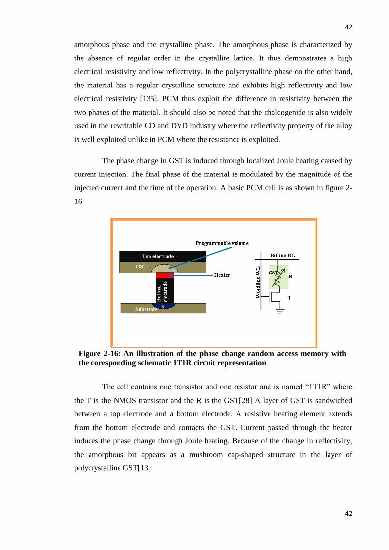
42
42
amorphous phase and the crystalline phase. The amorphous phase is characterized by
the absence of regular order in the crystallite lattice. It thus demonstrates a high
electrical resistivity and low reflectivity. In the polycrystalline phase on the other hand,
the material has a regular crystalline structure and exhibits high reflectivity and low
electrical resistivity [135]. PCM thus exploit the difference in resistivity between the
two phases of the material. It should also be noted that the chalcogenide is also widely
used in the rewritable CD and DVD industry where the reflectivity property of the alloy
is well exploited unlike in PCM where the resistance is exploited.
The phase change in GST is induced through localized Joule heating caused by
current injection. The final phase of the material is modulated by the magnitude of the
injected current and the time of the operation. A basic PCM cell is as shown in figure 2-
16
The cell contains one transistor and one resistor and is named “1T1R” where
the T is the NMOS transistor and the R is the GST[28] A layer of GST is sandwiched
between a top electrode and a bottom electrode. A resistive heating element extends
from the bottom electrode and contacts the GST. Current passed through the heater
induces the phase change through Joule heating. Because of the change in reflectivity,
the amorphous bit appears as a mushroom cap-shaped structure in the layer of
polycrystalline GST[13]
Figure 2-16: An illustration of the phase change random access memory with
the coresponding schematic 1T1R circuit representation

43
43
Two write operations exist for this memory: the SET that switches the GST
into crystalline phase by heating it above its crystallization temperature and the RESET
switches it back to amorphous phase by melt-quenching the GST [136]. Both operations
are controlled by electrical current whereby a high power pulse for the reset operation
heats the cell above the melting point of the GST and moderate power heats it above the
crystallization temperature but below the melting point of the GST. The stored data in
this memory cell is read by applying a small voltage across the GST. Because of the
large variance in the equivalent resistances of the SET and RESET status, it is possible
to sense the current through the cell. The read voltage should be such that it is
sufficiently strong to invoke detectable current but must also be low enough to avoid
write disturb. The data stored in the PCM cell can be accessed by wordline controlling
of the cell consisting of the GST in series with the NMOS as shown in figure 2-16.
Advantages of PCM include good signal sensing margin; the resistance ratio
between reset and set states is between 102-10
4[137], fast programming speed less than
300ns[138], excellent endurance of 1012
, good scalability as it does not utilize
electrons[13] and low cost[137]. Even though PCM claims good performance together
with the above mentioned advantages, there are nevertheless great challenges standing
in the path of it becoming really competitive to flash memory for commercialization,
one of which is the large programming current required for reset processes. This large
current requires large transistor cell size and thus makes it difficult for high density
PCMs to be achieved. Naele[139] argues that this cancels the advantage of scalability
of PCM claimed by others like Atwood[13].
2.5.2 Magnetoresistive Random Access Memory
This is a type of NVM that has been in development for about 20 years but
recently came into market with Freescale Semiconductor’s 4-MB offering. This
memory type is an application of spintronics, which combines the magnetic tunnel
junction (MTJ) and CMOS technologies [140, 141]. The basic cell structure is a 1T1R
similar to PCM but in this case the single resistor is the MTJ as shown in figure 2-17.
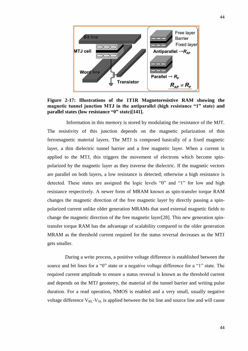
44
44
Figure 2-17: Illustrations of the 1T1R Magnetoresistive RAM showing the
magnetic tunnel junction MTJ in the antiparallel (high resistance “1” state) and
parallel states (low resistance “0” state)[141].
Information in this memory is stored by modulating the resistance of the MJT.
The resistivity of this junction depends on the magnetic polarization of thin
ferromagnetic material layers. The MTJ is composed basically of a fixed magnetic
layer, a thin dielectric tunnel barrier and a free magnetic layer. When a current is
applied to the MTJ, this triggers the movement of electrons which become spin-
polarized by the magnetic layer as they traverse the dielectric. If the magnetic vectors
are parallel on both layers, a low resistance is detected; otherwise a high resistance is
detected. These states are assigned the logic levels “0” and “1” for low and high
resistance respectively. A newer form of MRAM known as spin-transfer torque RAM
changes the magnetic direction of the free magnetic layer by directly passing a spin-
polarized current unlike older generation MRAMs that used external magnetic fields to
change the magnetic direction of the free magnetic layer[28]. This new generation spin-
transfer torque RAM has the advantage of scalability compared to the older generation
MRAM as the threshold current required for the status reversal decreases as the MTJ
gets smaller.
During a write process, a positive voltage difference is established between the
source and bit lines for a “0” state or a negative voltage difference for a “1” state. The
required current amplitude to ensure a status reversal is known as the threshold current
and depends on the MTJ geometry, the material of the tunnel barrier and writing pulse
duration. For a read operation, NMOS is enabled and a very small, usually negative
voltage difference VBL-VSL is applied between the bit line and source line and will cause

45
45
a current to pass through the MTJ[142]. It is necessary for the voltage to be small
enough so as not to invoke a disturbed write operation. The value of the current is
determined by the equivalence resistance of the MTJ which is compared with a
reference current by a sense amplifier and then decides whether a “0” or “1” state is
read.
The Freescale 4MB MR2A16A[143] based on the 0.18-μm CMOS technology
was the first commercially available MRAM. The key advantage is in its performance
and endurance. They are non-volatile and have the attributes of high speed operation
and unlimited read and write endurance. While this device still has a future, some issues
exist that need to be solved, among which include the current distribution in the word-
and bit-line during write operations (write disturbs)[144] and low readout signal during
read operation. Furthermore, the quest for high density integration is prompting the
move of MRAM devices from planar to 3-D cells. These future MRAM devices will
likely be based around spin valves or variations thereof that utilize the effect of giant
magnetoresistance (GMR) for their operations. Sautner et. al.[145], have found the
problem of integration of contacts into these spintronic devices nontrivial, as magnetic
materials are very sensitive to topographical variations created by contacts that can
introduce uncertainty in their behaviour.
2.5.3 Ferroelectric RAM (FeRAM)
A ferroelectric RAM is a type of NVM device with structure similar to the 1T-
1C DRAM but whose capacitor contains a ferroelectric material layer to achieve NVM
effects rather than a dielectric as in DRAM[146]. Thus a FeRAM utilizes a ferroelectric
FET with memory application based on the hysteresis behaviour of ferroelectric
material polarization with the application of an external electric field. Typical
ferroelectric material used is the lead zirconate titinate (PZT)[147] and SrBi2Ta2O9
(SBT)[148]. These materials show a reversible spontaneous polarization in the absence
of an electric field. The spontaneous polarization arises from the fact that the material
has a noncentrosymmetric arrangement of ions in its unit cell similar to an ABO3
perovskites structure [149] as shown in figure 2-18.
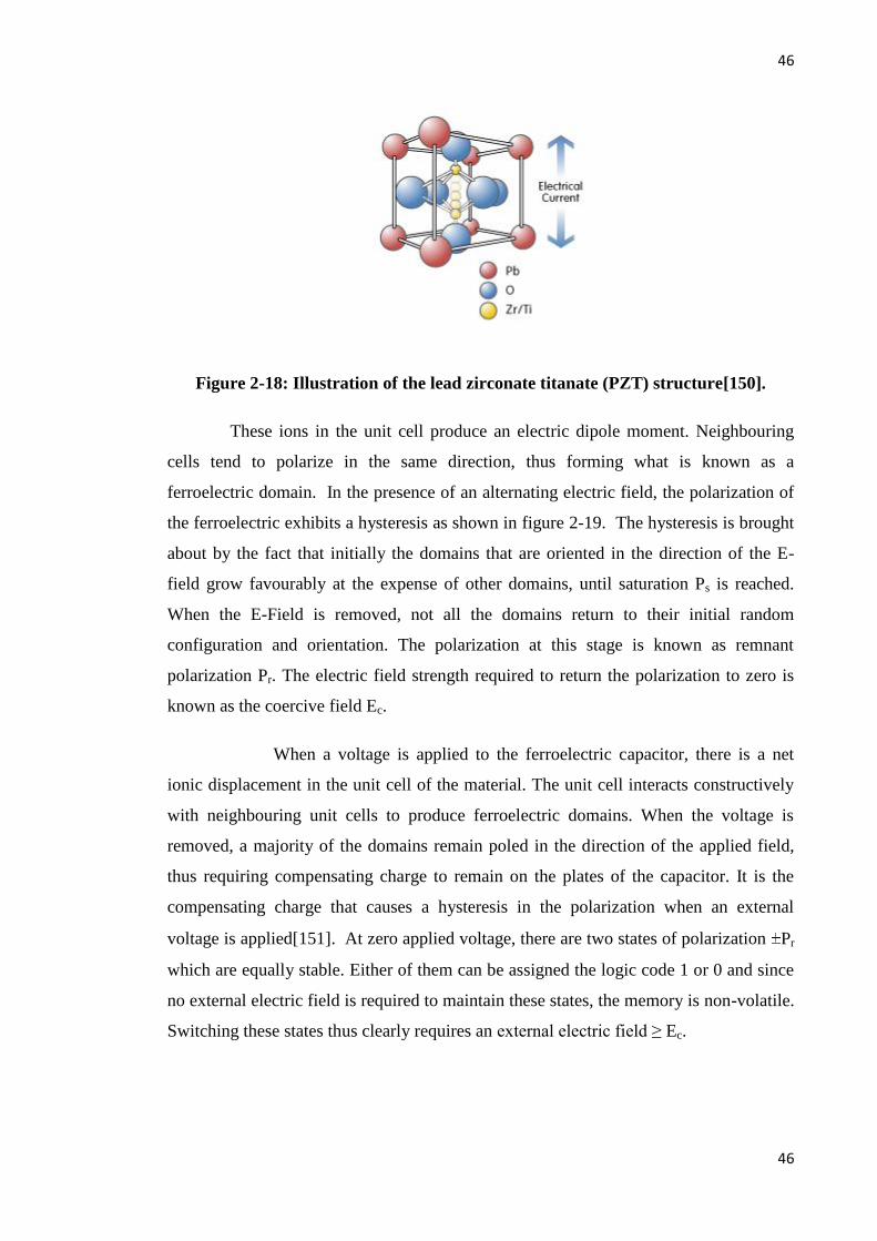
46
46
Figure 2-18: Illustration of the lead zirconate titanate (PZT) structure[150].
These ions in the unit cell produce an electric dipole moment. Neighbouring
cells tend to polarize in the same direction, thus forming what is known as a
ferroelectric domain. In the presence of an alternating electric field, the polarization of
the ferroelectric exhibits a hysteresis as shown in figure 2-19. The hysteresis is brought
about by the fact that initially the domains that are oriented in the direction of the E-
field grow favourably at the expense of other domains, until saturation Ps is reached.
When the E-Field is removed, not all the domains return to their initial random
configuration and orientation. The polarization at this stage is known as remnant
polarization Pr. The electric field strength required to return the polarization to zero is
known as the coercive field Ec.
When a voltage is applied to the ferroelectric capacitor, there is a net
ionic displacement in the unit cell of the material. The unit cell interacts constructively
with neighbouring unit cells to produce ferroelectric domains. When the voltage is
removed, a majority of the domains remain poled in the direction of the applied field,
thus requiring compensating charge to remain on the plates of the capacitor. It is the
compensating charge that causes a hysteresis in the polarization when an external
voltage is applied[151]. At zero applied voltage, there are two states of polarization Pr
which are equally stable. Either of them can be assigned the logic code 1 or 0 and since
no external electric field is required to maintain these states, the memory is non-volatile.
Switching these states thus clearly requires an external electric field ≥ Ec.

47
47
Figure 2-19: Illustration of the polarization behaviour of the ferroelectric PZT
with applied electric field
Two main types of FeRAM classified by readout exist. These are the
destructive read-out type(DRO)[152] and the non-destructive read-out (NDRO)
type[153]. The DRO type is the 1 transistor-1capacitor type similar in structure to
DRAM, easy to fabricate but has the disadvantage that it has low access speed and
number of endurance cycles. In this type, the ferroelectric layer of the 1T1C transistor is
separated from the CMOS layer by a thick interlayer dielectric (ILD). In the readout
operation, the data is destroyed and then written again. With the NDRO FeRAM, the
transistor is FET-type and difficult to fabricate but has the potential advantage of high
speed and high reliability. In the readout operation, the current between the source and
drain is sensed and the polarization does not reverse and thus data is not destroyed.
If an electric field is applied to the ferroelectric in a direction opposite to the
previous, this will cause the switching of the remnant domains, thus requiring
compensating charges to flow into the capacitor plate. If the field is in the same
direction as the previous field, switching does not take place, charge compensation does
not change and a reduced amount of charge flows to the capacitor plates. This property
is used to read a state or write a desired state into a ferroelectric memory. For instance if
the memory is in a negative state (-Pr) and a positive field is applied to it, there would
be a switching charge given by[154]
dtdt
dPAEAQ a
0 (2-20)
-
Pr
+
Pr

48
48
where A is the cell area, the permittivity, Ea is the applied electric field while P is the
polarization. Thus for a positive state and a positive field the charge stored is A Ea.
FeRAM write speeds are much higher than those of flash, typically in the ns
range. However, their bit density is lower than flash and they are more expensive.
2.5.4 Organic Memory Devices (OMD)
These are memory devices with active materials that are carbon-based as
opposed to traditional memory devices which are based on inorganic materials. OMDs
can be classed into three different categories namely: resistive switch and write once
read many times (WORM), molecular memory devices (MMD) and polymer memory
devices (PMD)[29]. All three classes have a similar structure of cross-point top and
bottom array of electrodes with different active organic materials sandwiched between
the electrodes to distinguish between the types of cells. The organic active layers are
usually deposited by spin-coating or by dip-coating. For WORM structure there is a
resistive polymer admixture sandwiched between the cross-point array of top and
bottom electrodes. Each cross-point of the bottom and top electrode with the resistive
material forms a memory cell. Depending on the type of resistive material used in the
cell, the device will short between electrodes giving a low resistance than the pristine
state while the second type acts like a blown fuse giving a higher resistance than the
pristine when a voltage pulse is applied across. For the MMD[155-158] structure the
sandwiched material between the cross-point top and bottom electrode arrays is
composed of small organic molecules. These molecules are packed in an ordered
manner so that one end of the molecule is electrically connected to the bottom electrode
while the other end is connected to the top electrode. When a voltage is applied across
the electrodes, the conductivity of the molecules is altered enabling data to be stored in
a non-volatile manner. Applying a voltage of opposite polarity reverses the situation and
data is erased. The PMD[159] is similar to WORM and MMD but in this case, the
sandwiched organic material also consists of deliberately introduced nanoparticles or
some other molecules in the admixture. Applying a voltage across a memory cell
invokes a change in the conductivity of the polymer admixture and thus allowing a bit
of data to be stored.
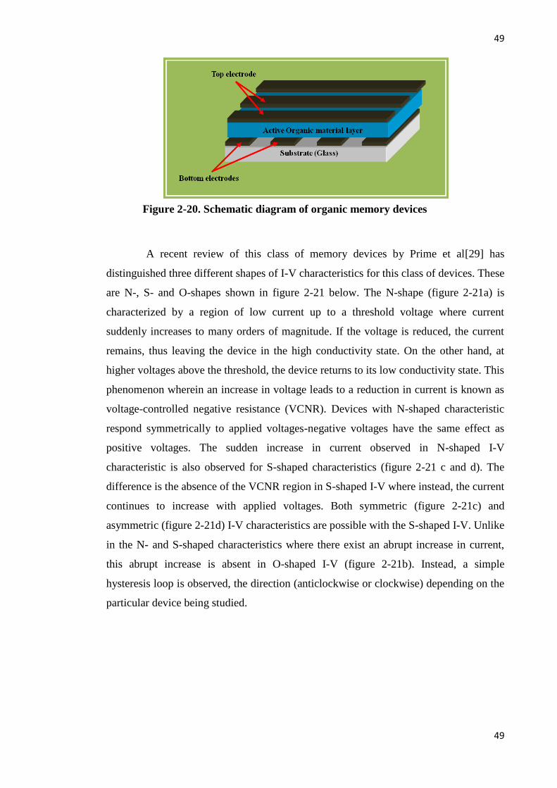
49
49
A recent review of this class of memory devices by Prime et al[29] has
distinguished three different shapes of I-V characteristics for this class of devices. These
are N-, S- and O-shapes shown in figure 2-21 below. The N-shape (figure 2-21a) is
characterized by a region of low current up to a threshold voltage where current
suddenly increases to many orders of magnitude. If the voltage is reduced, the current
remains, thus leaving the device in the high conductivity state. On the other hand, at
higher voltages above the threshold, the device returns to its low conductivity state. This
phenomenon wherein an increase in voltage leads to a reduction in current is known as
voltage-controlled negative resistance (VCNR). Devices with N-shaped characteristic
respond symmetrically to applied voltages-negative voltages have the same effect as
positive voltages. The sudden increase in current observed in N-shaped I-V
characteristic is also observed for S-shaped characteristics (figure 2-21 c and d). The
difference is the absence of the VCNR region in S-shaped I-V where instead, the current
continues to increase with applied voltages. Both symmetric (figure 2-21c) and
asymmetric (figure 2-21d) I-V characteristics are possible with the S-shaped I-V. Unlike
in the N- and S-shaped characteristics where there exist an abrupt increase in current,
this abrupt increase is absent in O-shaped I-V (figure 2-21b). Instead, a simple
hysteresis loop is observed, the direction (anticlockwise or clockwise) depending on the
particular device being studied.
Figure 2-20. Schematic diagram of organic memory devices

50
50
Figure 2-21: Illustration of different shapes of I-V characteristics of polymer
memory devices: (a) N-Shaped, (b) O-shaped, (c) Symmetric S-Shaped and (d)
asymmetric S-Shaped [29].
Organic electronic devices demonstrate unique advantages of easy fabrication
methods, low fabrication costs, high mechanical flexibility and versatility of the
material chemical structure over inorganic electronic devices; yet even with the
interesting performances exhibited by some of materials and devices [160, 161], they
are far from practical applications in memory. Even in the long run, they may only be
useful in short term memory devices, for instance in children’s toys, but not in durable
appliances like laptops and cellular phones.
2.6 Three-Dimensional Flash Memory
Among the emerging NVM, 3-D flash is widely considered the ultimate choice
to satisfy the needs of future envisioned memory, featuring low cost, high density, low
power consumption and better performance [32, 39, 40, 162-164]. Even some of the
alternative memory devices considered potential replacement of current flash memory
are also gearing towards 3-D cell structures to solve their scalability problems [145,
165]. In this section, a brief look at the different 3-D cell designs as well as the promises

51
51
of 3-D flash memory is presented. Less attention will be given to the type of memory
layer materials.
2.6.1 Different 3-D Memory Cell Designs
Since the 1980s when the concept of 3-D integration was introduced [166,
167], various cell designs have been researched. These include the FinFET[168-170],
multiple vertically stacked memory layer design[40, 163, 171, 172] , the surround gate
transistor[173], the vertical-Recess-Array Transistor[162, 174], the V-groove[15] and
lateral recess-channel array transistor[175]. The basic idea in the 3-D vertically-stacked
type memory is to stack multilayer cells atop one another to build a higher capacity chip
that would occupy less area than a single layer chip with the same capacity. All these
approaches promise higher storage capacity and speeds, better endurance, longer
retention time as well as better energy efficiency than their planar counterpart. They
however differ in the ease of fabrication and even in their performance, in which case
some will be more preferred than others.
As far as NAND flash is concerned, the most important breakthrough was the
Bit-Cost Scalable (BiCS) approach[39]. In the BiCS approach, Tanaka et. al., used a
drilled hole to define many memory layers simultaneously. More recently, other designs
have been proposed to solve various challenges in earlier technologies. These include
the pipe-shaped BiCS (P-BiCS)[176], the terabit-cell-array transistor TCAT[162], the
vertical-stacked-array transistor VSAT[177] and the vertical gate VG[175]. Some of
these are illustrated in figure 2-22 below. Vivid comparisons of the illustrated device
structures (table 2-2) have been made by Hsiao et. al.[178]. They note that scalability is
ultimately limited by the poly-channel thickness and the ONO thickness which in the
compared devices is the charge trap layer. With this, and the fact that for a reasonable
read current the channel dimension should be ~10 nm and the ONO thickness ~20 nm
for better reliability and good memory window, they have been able to estimate the
corresponding lateral scalability, and conclude that the VG device has the best
scalability in the 20s of nm (2x nm).
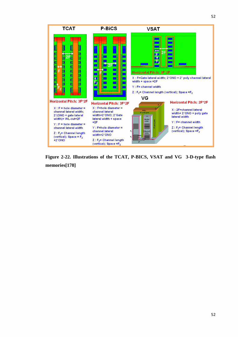
52
52
Figure 2-22. Illustrations of the TCAT, P-BICS, VSAT and VG 3-D-type flash
memories[178]

53
53
Table 2-2: Comparative summary of 3D NAND Flash array architectures in terms
of process, cell size, device structure, and scalability [178]
Another study carried out by Park et al.,[179] on the program/erase efficiency
and retention properties of 3-D SONOS flash memory cell array transistors has found
that the Gate All-Around cell array transistor (GAA-CAT) is more superior to the
Double Gate (DG-CAT) and the FinFET (structures shown in figure 2-23) in terms of
P/E efficiency, low voltage operation and integration density, and that the superiority is
more prominent with smaller substrate diameter DSi. Furthermore, they have shown that
this superiority results from the higher FN current in P/E conditions due to higher
electric field concentration effect rather than the gate controllability in the read
condition[178]
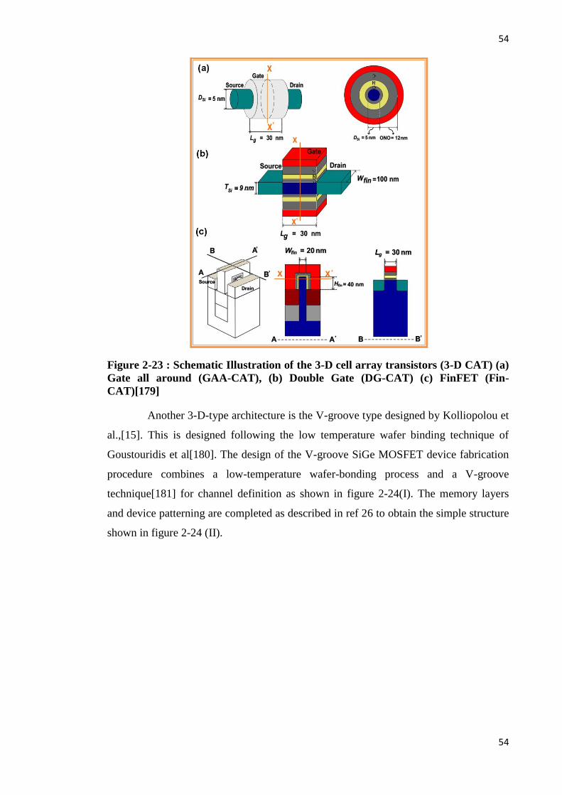
54
54
Figure 2-23 : Schematic Illustration of the 3-D cell array transistors (3-D CAT) (a)
Gate all around (GAA-CAT), (b) Double Gate (DG-CAT) (c) FinFET (Fin-
CAT)[179]
Another 3-D-type architecture is the V-groove type designed by Kolliopolou et
al.,[15]. This is designed following the low temperature wafer binding technique of
Goustouridis et al[180]. The design of the V-groove SiGe MOSFET device fabrication
procedure combines a low-temperature wafer-bonding process and a V-groove
technique[181] for channel definition as shown in figure 2-24(I). The memory layers
and device patterning are completed as described in ref 26 to obtain the simple structure
shown in figure 2-24 (II).

55
55
Figure 2-24: (I) An illustration of the V-groove MOSFET transistor device process
flow: (a) handling and device wafers; (b) low temperature bonding; (c) Si removal
and texturing of buried oxide; (d) Si anisotropic etching and buried oxide
stripping. (II) V-groove 3-D NVM transistor
The spin-on-glass bonding material used in the process is methylsilsesquioxane
(MSSQ). Kolliopolou and coworkers have demonstrated memory behaviour using this
transistor, shown in figure 2-24(II), with all process temperatures less than 400°C.
However, Au nanoparticles in a matrix of cadmium arachidate are used as the charge
trapping material instead the ONO charge trap or the usual alternative Si nanocrystals.
Here, the metallic nanoparticles offer a significant advantage over the semiconductor
nanocrystals as charge storage media because of their very large work functions, little or
no quantum confinement and excellent control over nanoparticles size. The large work
functions can improve the retention times of the devices without compromising on the
program/erase speeds.

56
56
2.7 Summary
In this chapter, the various memory types have been reviewed ranging from the
volatile SRAM and DRAM semiconductor memories to the non-volatile EPROM,
EEPROM and Flash. The historical evolution of NVM memory from the MIMIS,
through the EEPROM to Flash have been examined together with brief working
principles of these devices. More importantly, a detailed description of flash memory, in
terms of structure and operation mechanisms of programme, read and erase have been
explored. The problems plaguing these devices have been analysed and understood to
be relate to the down-scaling of the devices beyond a physical limit with consequences
requiring new cell designs or new materials to replace the current FG cell. The
challenges have been categorized into three main groups, physical scaling, electrical
scaling and reliability scaling challenges. Solutions proposed to solve some of these
challenges plaguing current flash have been analysed as well as their shortcomings.
They include the novel material devices such as PCM, MRAM, FeRAM and the
Organic memory devices and novel cell designs that includes the vertical direction in
the fabrication (3-D). The widely acclaimed 3-D memory cells with some selected type
designs have been discussed.
57
57
Chapter 3. Overview of Low-Temperature
Methods of Obtaining Polycrystalline Silicon
3.1 Introduction
Even though 3-D flash memory is widely acclaimed as the best way to deal
with the scaling difficulties of conventional planar FG flash memory, there is
nonetheless the process temperature requirements which do not agree well with the
current high temperature growth techniques currently in use with the planar cells. The
vertically stacked memory layer deign of 3-D flash memory demands the use of low
temperatures at fabrication so as to prevent thermal degradation of underlying device
layers as well as the maintenance of a low thermal budget [12, 37, 182-184].
The purpose of this chapter is therefore to review some low-temperature
process techniques of obtaining polycrystalline silicon (Polycrystalline silicon)
structures, a material often used as the FG in flash memory devices or as a channel in
thin-film transistors (TFT). The most widely used are solid-phase crystallization (SPC)
of amorphous silicon by furnace annealing or rapid thermal annealing RTA, excimer
laser anneal (ELA) crystallization of a-Si, metal-induced crystallization (MIC) and
metal-induce-lateral crystallization (MILC). The pros and cons of each these techniques
are also presented. Since amorphous silicon (a-Si) or hydrogenated amorphous silicon
(a-Si:H) are the main precursors of Polycrystalline silicon, a brief description of the
equipment of obtaining the material, particularly the radio frequency plasma-enhanced
chemical vapour deposition (RF-PECVD) reactor used in this research, is also
presented.
3.2 Structure and Electronic Properties of Polycrystalline
silicon
Silicon is found in group IV of the periodic table like carbon and it forms a
face-centred diamond cubic crystal structure with a lattice spacing of 0.543nm, with its
atoms covalently bonded to four neighbouring atoms[185] as shown in figure 3-1a
below. Two allotropes of silicon exist; amorphous silicon (a-Si) and crystalline

58
58
silicon[186]. Crystalline silicon is characterized by a regular pattern and long range
ordering of the unit cell while in a-Si, atoms form a continuous random network and
lack long range order but they do have a local order in the atomic scale. Furthermore,
not all atoms in a-Si are 4-fold coordinated as is the case with crystalline silicon.
Crystalline silicon can further be classed into single crystal and polycrystalline. In
single crystal silicon, the crystalline lattice is continuous and unbroken at the edges of
the sample with no grain boundaries, while in polycrystalline silicon the lattice is
composed of grains, with each grain containing a periodic array of atoms surrounded by
a layer of interconnectives or grain boundaries as shown in figure 3-1b. The grain
boundaries are narrower in size compared to the grains size, and act as carrier traps, thus
affecting the transport of charge carriers in the material[187]. On the borderline between
amorphous phase and polycrystalline phase is microcrystalline phase. Microcrystalline
silicon has a larger number of grain boundaries and smaller grain sizes compared to
polycrystalline silicon and contains a large number of very small grains embedded in
the amorphous matrix of the material[188].
The grain size and morphology are very important parameters that affect the
FG memory characteristics. Luoh et al.,[189] have recently demonstrated that small
(micro-grains) of FG Polycrystalline silicon have better endurance, tighter threshold
voltage distribution and better gate-coupling ratio than large grains. Their findings
Figure 3-1: Illustration of (a) FCC Structure of a unit cell of silicon and (b)
poly-Si crystal grains separated by grain boundaries.
59
59
conform with previous work by Maramatsu et al.,[190] who had demonstrated that the
grain size of FG Polycrystalline silicon dominates the erase characteristics of flash
memory and that small gain size exhibited a narrower erase distribution. Nkansah, F.
D. and Hatalis, M. [191] have shown experimentally that Flash EEPROM FG
Polycrystalline silicon morphology, as a result of the deposition and doping process of
choice, could enhance localized FN tunnelling of energetic electrons. In their study, the
Polycrystalline silicon FG was deposited on tunnel oxide in 3 different ways: 1)
sandwich of undoped plus phosphorus in-situ doped; 2) undoped followed by an
implant; and 3) in situ doped. They found that the FG polycrystalline silicon grains
obtained in the case where the stack on the tunnel oxide was deposited in the sandwich
undoped plus phosphorus in-situ doped case exhibited the smallest grain sizes and
smoothest morphology compared with grains from the others methods. Devices from
this also showed a much reduced FN tunnelling currents compared to the others.
Smaller Polycrystalline silicon grains also means more grain boundaries that will
enhance the electric field and consequently enhance the erasing speed of the memory
cell[192]. Thus producing polycrystalline silicon for FG in flash memory requires the
choice of the right method and right temperature, as these fundamentally affect the
quality of material grown.
While small grained polycrystalline silicon may be beneficial to the FG, large
grains have been found to produce polycrystalline silicon TFT channels with high
charge carrier mobilities. Recently, Yin et al.,[193] have obtained very good carrier
mobility of 289 cm2/Vs and on-off current ratio of 5.1 x 10
6, with a scalable 3-D fin-like
large-grain polycrystalline silicon channel obtained by super lateral growth laser anneal
crystallization technique. Kuo et al.,[194] have also recently successfully developed and
fabricated a vertical n-channel large grain polycrystalline silicon with field effect
mobility of 553 cm2/Vs by a Ni-silicide-induced lateral crystallization (NSILC)
technique. They obtained an on-off current ratio of ~ 107 with a steep sub threshold
voltage swing of 180 mV/dec. The electrical properties of enhanced polycrystalline
silicon TFT channels are improved because with large and regular grains, the number of
grain boundaries in the channel is reduced, thus reducing the resistance to carrier
mobility along the channel.

60
60
It is noteworthy that the grain boundaries that surround the polycrystalline
grains are rich in silicon dangling bonds (3-fold coordinated silicon atoms). Cleri et
al.,[195] have shown that the atomic structure of these grain boundaries is similar to that
of bulk a-Si. These dangling bonds create charge carrier trap sites, which introduce
localized energy levels within the silicon band gap. The densities as well as the location
of these dangling bond defects have a profound impact on the electrical properties of the
resulting polycrystalline silicon films. Lin et al.,[196] have demonstrated the effects of
dangling bond density on memory characteristics with the SONOS-type Flash memories
with Polycrystalline silicon channel. They found that dangling bonds present along the
grain boundaries in the polycrystalline silicon channel influence significantly the flash
memory device reliability characteristics in the aspects of charge storage, drain
disturbance, and gate disturbance. These dangling bonds can be passivated by atomic
hydrogen[197, 198]. The atomic hydrogen diffuses through the silicon film and bonds
with Si at the dangling bond defect site. This improves the electrical properties of
polycrystalline silicon which results in an increase in charge carrier mobility, decreased
leakage currents and increased threshold voltage of TFTs made of this material[199]
However, electrical stress can also cause weak Si-H bond breakage which may also
affect device reliability[200]
3.3 Growth Methods of Polycrystalline silicon
Polycrystalline silicon is commonly deposited by chemical vapour deposition
(CVD) through the thermal decomposition or pyrolysis of silane at temperatures >
500°C using thermal atmospheric pressure chemical vapour deposition (APCVD) or
low pressure CVD (LPCVD) reactor or Hot-wire CVD. The pyrolysis of silane involves
several possible chemical reactions, e.g.,[53]:
SiH4 → Si + 2H2
SiH4 → SiH3 + H
SiH4 → SiH2 + H2
A multi-step process can also be used where amorphous silicon is deposited by
a CVD process (APCVD, LPCVD, HWCVD, or plasma-enhanced CVD) and

61
61
subsequently crystallized through several means such as solid-phase crystallization,
laser annealing, chemical annealing, etc, some of which methods will be expatiated on
in subsequent sections in this chapter.
The deposition of quality polycrystalline silicon involves the control of critical
deposition variables which include the pressure, temperature and the silane
concentration. For doped Polycrystalline silicon, the concentration of the dopant is also
of critical importance. The deposition rate of Polycrystalline silicon using the LPCVD
reactor is usually between 10-20 nm/min and the rate follows the Arrhenius
equation[201]
)exp(KT
EAR a (3-1)
where R is the growth rate, Ea the activation energy which is ~1.7 eV, T the deposition
temperature, k the Boltzmann constant, q the electronic charge and A is a constant.
There are two reaction regimes for the deposition of Polycrystalline silicon by thermal
CVD techniques. These are the mass-transport limited regime and the surface-reaction
limited regime. Based on the Arrhenius equation, it is observed that the deposition rate
increases with an increase in temperature. However, this also depends on the amount of
unreacted silane on the reaction surface. There would be a minimum temperature
wherein the rate of deposition is faster than the rate at which unreacted silane arrives the
deposition surface. Beyond this temperature, the deposition rate can no longer increase
due to the absence of silane which is the precursor for polycrystalline silicon. This
reaction is thus said to be mass-transport limited. In this regime, the deposition rate
depends on the gas flow and concentration as well as the reactor geometry. Surface
reaction limited regime occurs when the rate at which unreacted silane that arrives the
reaction surface is greater than the rate at which polycrystalline silicon deposition
occurs. Such a deposition rate is dependent on the temperature and the silane
concentration and often results in excellent film thickness uniformity and good step
coverage. For VLSI manufacture, polycrystalline silicon deposition at less than 575°C is
very slow to be practical and above 650°C, thickness uniformity is poor[202].

62
62
3.4 Plasma-enhanced Chemical Vapour Deposition (PECVD)
Apart from growing Polycrystalline silicon directly by APCVD or LPCVD at
temperatures greater than 600°C, the material can also be obtained by crystallization of
a-Si or a-Si:H. Three crystallization methods are often employed. These are solid-phase
crystallization (SPC) of a-Si by thermal annealing, excimer laser annealing (ELA) and
metal-induced (lateral) crystallization (MIC) or (MILC). The a-Si or a-Si:H can be
grown using a variety of techniques like LPCVD or APCVD at less than 600°C,
sputtering, hot-wire CVD or PECVD. PECVD offers a number of advantages over the
other methods that includes low temperature processing.
PECVD is a method of depositing thin films of silicon and dielectrics on
substrates using plasma (ionized gases) at temperatures of 400°C or less. Plasma is the
4th
state of matter after solid, liquid and gas and it is obtained when a gas is heated
enough such that its atoms collide with each other knocking off electrons in the
process[203]. It can also be excited and sustained electrically by direct current, radio
waves or microwaves.
Thus different plasma-assisted chemical vapour deposition sources exist. These
include the conventional capacitively coupled radio frequency (RF) discharge sources
(plane parallel geometry, coaxial, RF diode), inductively coupled RF discharge source,
electron cyclotron resonance (ECR), helicon, helical resonator and surface wave
sources[204]. For DC plasma sources, conducting electrodes are required. It is however
not possible to deposit dielectric films by DC plasma technique because the electrodes
exposed to the plasma gradually get covered with the insulating dielectric material being
deposited. This causes the DC discharges to quickly get extinguished soon after it is
ignited because electrons and negatively charged ions accumulate on the surface of the
insulating material that covers the anode and recombine with the available ions. The
cathode also gets covered with positively charged ions.
Nonetheless, a solution to this exists, which is the use of alternating current
(ac) plasma. In this case, the alternating electric field applied across the electrodes in the
chamber makes each electrode act alternately as the cathode and anode during each half
ac cycle. Above a certain critical frequency[205], a temporary DC discharge is sustained

63
63
when the breakdown potential is surpassed at each half cycle. The ions with
instantaneous positions at the anode cannot reach the anode before the field is reversed.
The distance travelled by the ions during the half-cycle is less than the thickness of the
plasma sheath. Thus a positive space charge is partly retained between the two half-
cycles of the alternating electric field and helps the re-initiation of the discharge which
results in a potential difference across the plasma sheath known as the self-bias. Below
this critical frequency, it is not possible to sustain such a temporal DC discharge. This
critical frequency is defined as the reciprocal of the time taken by a positive charge to
move between the two electrodes.
Typical radio frequency for the conventional RF-PECVD reactor is 13.56 MHz
and the self bias generated usually vary between 100V to 1KV depending on the RF
power input and pressure[204]. Excitation frequencies in the low frequency range of
approximately 100 KHz would require several hundred volts which would lead to high
ion bombardment of the reaction surface. Very high frequency VHF-PECVD (e.g. 60
MHZ) [206] and ultra-high frequency UHF-PECVD (e.g. 500 MHz)[207] are also often
used to obtain high deposition rates.
Unlike the APCVD and LPCVD where deposition temperatures are high and
energy for the reaction is supplied solely by heating, deposition temperatures in PECVD
are typically ≤ 400°C and the energy for the chemical reaction is provided by the heated
cathode and the radio frequency (13.56 MHz) generated ac discharge. Further
advantages of PECVD over LPCVD and APCVD include less dopant diffusion and the
use of wider range of substrates because of low deposition temperatures. More so, by
varying system parameters such as vacuum chamber pressure, RF power, temperature
and gas flows allows the user to adjust a film’s physical properties, e.g. refractive index,
growth rate and film density.
3.4.1 The Capacitively Coupled RF PECVD Reactor Design
The schematic diagram of the PECVD system used to deposit silicon films
described in this thesis is illustrates in figure 3-2. It is a capacitively coupled RF-type
PECVD reactor. The system (shown in Appendix 2) is composed of two reactors;
Master and Slave (reactive ion etcher RIE). Films are deposited using the master
64
64
reactor. The deposition process is based on electron impact dissociation of process gases
which in this project is silane (SiH4) for the deposition of amorphous silicon (or SiH4,
ammonia (NH3) and nitrogen (N2) for the deposition of silicon nitride) at low pressures.
The cylindrical master reactor chamber is composed of two capacitively coupled
electrodes separated by a 40-mm gap when the chamber door is closed. The bottom
electrode called the platen which is of diameter 240 mm is electrically grounded and is
also heated from beneath. It is on this electrode that the substrates for film deposition
sit. The upper electrode is driven by an ENI ACG-5 XL 13.56 MHz RF generator with a
manual impedance matching unit and also acts as a shower head through which process
gasses are uniformly injected into the reactor chamber across the entire diameter. The
RF generator generates the plasma which is confined within the space between two
electrodes. The flow rate of gases through the shower head is controlled by a system of
6 Tylan FC-260 mass-flow controllers (MFCs) in a gas pod. The MFCs monitor the gas
flow rate with a thermal sensor and regulate it with a thermal expansion valve. This
delivers the gas at a flow rate proportional to the input signal voltage manually set by
means of a potentiometer on the front panel of the microprocessor unit. The
temperature of the platen is measured by a thermocouple that is connected to the
Honeywell Temperature Controller capable of maintaining the lower electrode at a
preset temperature ±1°C. The reactor is cooled by a BETTA-TECH CONTROLS chiller
that pumps cool water in to cool the electrodes. The reactor chamber is evacuated and
gases are extracted via a port at the centre of the chamber beneath the platen. This is
done by a combination of a roots pump, model- Edwards Mechanical Booster 500A and
a rotary pump, model- Edwards High Vacuum Pump E2M 80. This pumping system is
capable of pumping the reactor chamber down to a base pressure of less than 5 mTorr.
Process gas pressures during depositions are controlled by a throttle valve. During
system operation, process parameters like RF power, pressure, and flow rate are input
via push button keys on the microprocessor unit. The maximum allowable RF power by
the system is 300W, and permissible maximum temperature is 400°C. Processes in this
system are manually timed using a digital stop clock. A picture of the deposition system
is presented in appendix 2.

65
65
3.5 Deposition of a-Si or a-Si:H
Microcrystalline silicon, a-Si and a-Si:H have been deposited by various low
temperature and plasma techniques including Hot Wire CVD, ECR-PECVD and RF-
PECVD[208, 209]. A detail description of the growth of a-Si and a-Si:H has been given
by Street, [53] and various growth models have been described, e.g. by Matsuda et
al[210-215] and Flewitt et al.,[216]. Only a summarized deposition process is presented
in this section.
During the deposition process, source gases (SiH4 and H or Ar for instance)
that enter the reaction chamber are ionized by the RF ac discharge. The collision of
electrons with the gas molecules lead to several reactions such as excitation,
dissociation and ionization to produce positively and negatively charged ions as well as
neutral radicals as energy is transferred from the electron to gas molecules. A glow
discharge or photon emission is observed as the excited gas molecules in the higher
electronic states recombine or decay to the ground state with the emission of light[53].
Figure 3-2: Schematic diagram of the Master Unit (PECVD unit) of the
Master/Slave PlasmaLab reactor system
66
66
These gas molecules can also be excited to higher vibrational or rotational states. The
neutral radicals and the ions formed further collide with each other and with SiH4 giving
a very complicated chemistry. However, for typical low power plasma the fraction of
radicals and ions is very small ~ 10-3
, thus most collisions are with SiH4. The radical
species diffuse to the substrates surface and the positive ions are also accelerated to the
substrate by the sheath that forms above the earthed lower electrode which holds the
substrate where material deposition takes place. Negative ions are however confined to
the bulk plasma and may lead to particulate formation when they recombine with the
silane radicals to become larger negative ions[217]. At the growth surface, the film-
forming radicals diffuse to growth sites or desorb from the surface while hydrogen is
released from the network. It is generally accepted that the SH3 radical (silyl) is the
predominant growth precursor of quality a-Si:H[53].
While deposition conditions such as gas flow rate, gas pressure, temperature
and RF power influence the film quality, high quality a-Si:H are often grown at low RF
power and gas pressures of 0.1-1Torr[53]. It is also noted that a high concentration of
hydrogen dilution of silane can cause the deposited films to become microcrystalline
rather than amorphous with small grain sizes, while dilution with argon causes films to
grow with columnar morphology, with columns oriented in the direction of growth[53,
218, 219]. The concentration of atomic hydrogen in the film varies between 8 and 40
at.% and decreases with increase in temperature.
3.6 Conversion of a-Si and a-Si:H to Polycrystalline silicon
The a-Si or a-Si:H films grown by RF-PECVD or other method are the
converted to polycrystalline silicon through different methods namely SPC of a-Si,
ELA, MILC, MIC. SPC by furnace annealing at 500-600°C is the simplest and most
widely used but its long anneal time (hours-days) especially at low temperatures[220] is
a call for concern. SPC by RTA of a-Si is usually performed at temperatures in excess
of 700°C for a short duration (in minutes). Pulsed and continuous laser annealing by
selective melting part of a-Si film and allowing it to crystallize has been used to obtain
Polycrystalline silicon films. Combinations of laser anneal and SPC has also been
used[221]. Metal-induced (lateral) crystallization of a-Si through the deposition of a

67
67
metal film on a-Si and annealing the composite has also resulted to polycrystalline
silicon[222, 223]. These methods are briefly discussed below.
3.6.1 Solid-Phase Crystallization
Solid-phase crystallization of a-Si can be performed through furnace annealing
at 550 ~ 950°C for several hours[54, 224], single step rapid thermal annealing (RTA) at
700 ° C for several minutes[225-227] or multistep rapid thermal annealing[228]. The
amorphous and crystalline phases of silicon differ by a fairly well defined free energy
difference of ≈ 0.1 eV per atom at 300K [229]. The amorphous phase has a higher free
energy than the crystalline phase. Thus there is always a driving force towards
rearranging the positions of the atom into those of the crystal. This can be accomplished
by raising the temperature to a certain extent and maintaining it for a practical time, e.g.
hours, so as to give the atoms enough mobility for the rearrangement.
SPC of a-Si takes place by nucleation of crystalline clusters with ordered
arrangement of atoms within their disordered surrounding matrix. The crystal clusters
then reach a critical size estimated to be 2-4nm at 650°C [230] before growing
spontaneously. However, for nucleation to occur, bond breaking has to occur in the a-Si
material so as to allow for atomic rearrangement. Once the critical size has been
reached, growth proceeds by the displacement of atoms from the amorphous phase to
the crystalline phase through the interface between the crystalline cluster and the
amorphous matrix. This situation corresponds to that in which the free energy gained by
converting the a-Si to the crystal is greater than the surface energy for the creation of the
interface between the a-Si matrix and the crystalline cluster. Complete crystallization of
the a-Si film is attained when the crystal clusters grow into the amorphous matrix and
impinge on each other. The activation energy of nucleation depends on the properties of
the amorphous silicon film. Values ranging between 4.9 - 9 eV have been reported[231,
232]. For crystal growth, the activation energy values between 2.3-2.7 have also been
reported [233, 234]. Iverson and Reif have provided a theoretical analysis of the
transient nucleation of a-Si which suggests that the final grain size rf at the completion
of crystal growth depends on the nucleation rate N and crystal growth velocity Vg in the
course of crystallization. The final grain size is given by[233]
68
68
3/1
Nr
g
f (3-2)
Thus large grain sizes are obtained for high crystal growth rates and low nucleation
rates. This is achievable at < 700°C since nucleation activation energies are
comparatively higher than those of crystal growth.
As aforementioned, atoms in the amorphous phase require enough energy for
them to gain mobility and rearrange themselves into an ordered manner to form the
crystalline phase. This energy can be achieved in various ways. In SPC, the simplest
way and most frequently used technique is annealing of the a-Si films in a furnace at
temperatures in excess of 500°C in vacuum or in the presence of an inert gas usually
nitrogen or argon for long hours (at time > 20 hr). Other techniques involve heating the
a-Si films to temperatures in excess of 700°C for a few minutes for complete
crystallization to occur. This method is known as rapid thermal annealing (RTA)[235].
Even though with this method temperatures are > 700°C higher than glass softening
temperatures [236] glass substrates can still be used. The short duration of the annealing
process minimises the thermal stress the glass substrates. The crystallization kinetics for
these two annealing techniques (furnace vs. RTA) are different. Nucleation is reported
to be faster in RTA than in furnace annealing [237]. It is suggested that the difference is
due to the fact that in RTA light spectra (from tungsten-halogen lamps for example) are
used while only the resistive coil is used in furnace annealing. The more energetic
photons produced by the tungsten-halogen lamps used to heat the a-Si break the weak
and strained bonds in the film and create photo carriers which subsequently recombine.
The broken bond sites then serve as recombination centres for more photo carriers
leading to localized heating and thus favourable sites for nucleation [237]. The grain
size of the resulting Polycrystalline silicon from RTA is smaller than those resulting
from furnace annealing because of the increase in the number of nucleation sites in the
RTA process.
3.6.2 Laser Annealing
Various laser annealing techniques of a-Si have been utilized to obtain
polycrystalline silicon. The most widely reported is the excimer laser annealing

69
69
(ELA)[238-243] with commercial interest mostly focused on the production of high-
speed, low-temperature TFTs for large area electronics[244-248] and for 3-D integrated
circuit[193]. The mechanism of laser annealing is based on the fact that during
irradiation of the film with photons of energy hν greater than the band gap of the film
material, the laser (photon) energy is absorbed leading to electron-hole pairs excitation
across the band gap. The excited carriers rapidly thermalize and transfer energy to the
lattice by phonon emission in a picoseconds time scale [249].
It should be noted that for the ELA of a-Si:H to be carried out, the a-Si:H must
be dehydrogenated due to the fact that a-Si:H films (especially from PECVD) have a
high content of hydrogen and consequently hydrogen bubbling or ablation could occur
during the ELA process. Dehydrogenation is thus usually performed through furnace
annealing at 500 °C before ELA. Nonetheless, ELA of a-Si:H has been reported for
films a-Si:H from catalytic CVD with a hydrogen content of 1.3 at.% [250]. Even so,
surface ablation was observed for laser energy density of 375 mJ cm-2
although
hydrogen bubbling was not observed.
Figure 3-3 is an illustration of laser annealing technique. In the case where the
a-Si film is irradiated with an excimer laser pulse in a duration of τ = 30 ns, the laser is
absorbed through a depth in orders of 10-6
cm. Given D the thermal diffusivity of the a-
Si film (~10-3
cm2s
-1 [251]), the heat diffusion length in the film amounts to (Dτ)
1/2
which is ~10-5
cm at elevated temperature [252]. It thus implies than under such
conditions, most of the energy from the laser pulse will be localized within the first 100
nm of the film (from the surface) whereas the underlying substrate will remain cool
(nearly unheated).
Within a very short time (30-50 ns) of pulse laser irradiation, various
transformation of the a-Si film can occur. Unlike in normal heating circumstances
where crystallization of a-Si occurs before it melts, this is not so in pulse laser annealing
in which crystallization is bypassed and a-Si is directly melted by a first order phase
transformation because the laser heat supply is too fast.

70
70
Noting that the melting temperature of a-Si (~225°C) is less than that of crystalline
silicon [253], the consequence is that the melted a-Si (liquid-Si) can be severely under-
cooled relative to the equilibrium melting temperature of c-Si. Nucleation can therefore
occur in the liquid-Si in the event that the under-cooling is maintained for a longer time.
This nucleation can thus trigger the explosive growth of crystals in the underlying a-Si
[253]. The downward penetration of the liquid-Si layer due to latent heat of
crystallization melts the adjoining a-Si and thus leaves behind fine grain Polycrystalline
silicon [254]. Subsequently in the process, the liquid-Si permeates through the entire a-
Si film and depending on the energy density of the laser pulse, the fine grains can be re-
melted by the primary melt front that has penetrated the grains. Re-melting will not
occur if the energy density of the laser pulse is not high enough. The film will rather
solidify into fine grain Polycrystalline silicon. On the other hand, high-enough laser
pulse energy density will mean that the fine grain region will be completely melted and
the liquid-Si allowed to cool at the end of the pulse. Consequently, under-cooling again
occurs and homogenous nucleation takes place in the melt thus leading to small grain
Polycrystalline silicon growth [255]. In the situation where not all small grain
Polycrystalline silicon are melted and some survive, super-lateral growth (SLG) occurs
in which large grains are obtained due to crystal growth from the surviving small seeds
(Polycrystalline silicon grains) [256]
Very good performing polycrystalline silicon TFTs have been obtained with
SLG ELA Polycrystalline silicon [256]. Furthermore, improved advanced laser
Figure 3-3. Illustration of laser annealing of a-Si film
71
71
crystallization techniques such as solid lateral solidification (SLS) have been employed
to achieve larger Si grain sizes with improved carrier mobilities in TFTs [257, 258].
Brunet et al.,[259] employed this technique to crystallize nanocrystals NVM devices
which have shown program and erase behaviour. Furthermore, large elongated grains
with almost parallel grain boundaries have been obtained using lateral thermal gradients
established through the use of patterned antireflective strips [260, 261]. These
antireflective strips of SiO2 or Si3N4 modulate the absorption of the laser energy. Also
noteworthy is the fact that while much is still being done to better the ELA
crystallization technique and materials obtained thereof, laser annealed polycrystalline
silicon films with single crystal-like TFT mobility values of 640 cm2/Vs and 400
cm2/Vs for n and p-channel TFTs respectively have been achieved [262, 263].
The ELA crystallization techniques also have some drawbacks; the processing
window for SLGs ELA is very narrow and requires excellent beam uniformity and good
pulse-to-pulse reproducibility. Very slight changes in the laser energy density and
silicon film thickness can result in variations in the average Polycrystalline silicon grain
size thus leading to device non-uniformity [256, 264]. For large area processing,
sophisticated beam homogenizers are required which are even more costly than the
laser. Beam overlap is also a source of non-uniformity since there is always an energy
gradient at the edges. In addition to these drawbacks, pulsed laser anneal crystallization
leads to surface roughness with high protuberances, especially at grain boundaries [264,
265]. This can lead to high leakage currents in devices with pulsed laser crystallized
Polycrystalline silicon.
3.6.3 Metal-Induced (Lateral) Crystallization
Metal-induced crystallization (MIC) is another low temperature method of
converting a-Si and a-Si:H into Polycrystalline silicon at temperatures slightly lower
than in furnace annealing or RTA. In this method, metallic particles are introduced in
the a-Si film and the composite a-Si-metal alloy is annealed. Carlsson et al.,[222] have
used a semi-empirical model for predicting the crystallization temperature variation
with composition for a-Si-metal based binary alloys. Their results suggest that metallic
impurities in the a-Si lead to reduced crystallization temperature of the film.
Furthermore, based on the calculated heat of formation of the Si-based amorphous

72
72
alloys, they observed that the crystallization temperature of the a-Si film decrease with
increase in the concentration of the metallic impurities up to ~ 20 at.%.[222].
A variant of MIC is the metal-induced lateral crystallization (MILC)[266] in
which the metallic impurities are selectively introduced at particular locations in the a-
Si film and the film crystallizes laterally away from the metal impurity region. Figure 4
is an illustration of the MIC and MILC processes. Metallic particles are deposited on the
a-Si or a-Si:H films and the composite is furnace annealed at or laser annealed to induce
crystallization.
Various methods are used to introduce the metallic impurities into a-Si films.
These include simply depositing a thin layer of the metallic film on the a-Si film[267,
268], ion implantation[232] or co-depositing with the a-Si film during growth[269].
After forming the alloy, crystallization follows either by SPC through furnace
annealing, RTA or by laser annealing. Various metallic impurities have been used such
as Ni, Al, Pd, Au, Co or combinations of these metals [270-283]. A plausible
explanation for the enhanced crystallization of a-Si or a-Si:H by MIC or MILC is that
for eutectic-forming metals with Si such as Al and Au, the dissolution of their atoms in
a-Si weaken the Si-Si bonds and enhance the nucleation and growth of Si crystals[269].
There are further suggestions that the breaking of metastable metal-Si bonds facilitate
the local rearrangement of atoms to obtain the crystalline structure[284]. In the case of
reactive metal alloys or silicide forming metals like Ni, Cu, Co, Pd etc, Heyzelden et
Figure 3-4: Illustration of the MIC and MILC processes
73
73
al.,[285] suggest that the formation of sillicides with lattice constant close to that of Si is
a necessary prerequisite for the MIC or MILC process. In these processes, the
crystallization time and temperature is quite reduced compared with the SPC by furnace
annealing technique. Early Polycrystalline silicon TFT made by MILC used Ni and
crystallization time and temperature reduced to 5hr and 500°C respectively[286].
3.6.4 Advantages and Disadvantages of MIC, MILC SPC, and ELA of
a-Si Techniques
As observed in the preceding sections, the current industrial techniques of low
temperature Polycrystalline silicon each have their pros and cons. The properties of the
Polycrystalline silicon films obtained inherently depend on the route through which the
films are obtained. Likewise, the purpose for which the films are intended to be used
would determine the method by which they are obtained. Polycrystalline silicon is
wildly used in display technology such as active matrix liquid crystal displays and
active organic light-emitting diodes which use glass as substrate for the material. With
the increasing need of integrating memory into systems-on-panel or glass (SOP or
SOG) and for low cost production of memory transistors, glass as well as flexible
(plastic) substrate material are required in place of the more expensive silicon wafers.
This in turn requires that process temperatures must be low enough so that these
substrates will not be deformed during processing. Furthermore, in the case of 3-D
memory, where memory layers are stacked vertically on other device layers, the need
for proper control of process temperatures is vital as high temperatures may thermally
degrade underlying memory layers apart from stressing the substrates. Therefore, even
with the use of silicon as substrate material, low temperature processing for 3-D
memory is vital.
The processes discussed above for preparing low temperature polycrystalline
silicon each have particular characteristics that affect the crystalline quality. As
compared to ELA, MIC and MILC technique of obtaining Polycrystalline silicon, SPC
is the simplest and most commonly used process. However, its long hours of annealing
at relatively high temperatures is a disadvantage which eliminates it from any device
application requiring process temperatures to be less than 400°C. On the other hand,
while ELA crystallization can provide active layer Polycrystalline silicon with large
74
74
grains, the technique is very expensive. More so, the random positioning of grain
boundaries leads to large device-to-device variations. Furthermore, apart from the
narrow process window, the difficulty in controlling the laser beam density can lead to
highly non-uniform polycrystalline silicon films with high surface roughness and high
protuberances [256, 264, 265]. Even with the novel techniques reported for allowing
controlled formation of grain boundaries by ELA through air-gap formation, two-pass
laser crystallization or the introduction of buried crystallization seeds [287-289], it is
still unclear how to effectively control grain formation.
The crystallization time in SPC is reduced considerably using the MIC
technique. However, metal impurities from this technique will degrade device
performance[290] and for flash memory, these could be a major source of high leakage
currents. Metal impurities (traces) concentration in MIC is reduced by selectively
depositing the metal only in the specific regions (source and drain regions in TFTs) and
performing MILC. This allows metal particles to move laterally across the channel,
creating Polycrystalline silicon films with lower metal contaminants. The problem with
MIC and the improved variation MILC is that apart from the high leakage currents
resulting from the metal impurities, the anneal time is still long and temperatures are
still considerably greater than 500°C.
3.7 Summary
In this chapter, the commonly-used deposition techniques and crystallization
methods of a-Si have been reviewed. Particularly, the merits of SPC, ELA, MIC and
MILC as well as their shortcomings have been examined. SPC by furnace and even
RTA are found to utilize high operating temperatures. The problems with ELA, MIC
and MILC are more related to the performance concerns of devices. Polycrystalline
silicon obtained by these techniques are likely to show non-uniformity, rough surfaces,
high protuberances (ELA), high metal density of contaminants (MIC and MILC). Thus
the need of an alternative low temperature Polycrystalline silicon growth technique at ≤
400°C that would produce better quality Polycrystalline silicon grains is of importance
to the flash memory industry and other industries requiring polycrystalline silicon.
75
75
Chapter 4. Characterization Methods of Silicon
Films and Memory Devices
4.1 Introduction
The chapter presents a review of the characterization techniques of all the
material films grown or deposited in this research, as well as all the devices fabricated.
The aim is to study the effects of the new technique on the properties of films and on
the devices fabricated with the films. A crucial requirement of 3-D memory devices is
for process temperatures to be low (≤ 400°C ) so as to avoid damage of underlying
device layers and reduce the thermal budget. It is thus vital to understand how the
growth parameters in this new low temperature technique modify the structural and
electronic properties of silicon films, as well as their memory characteristics when they
are used as the floating gate in flash memory device. Material properties of interest here
are:
Band gap,
Hydrogen content and the chemical composition of the film,
Conductivity of the films,
Charge storage ability of the films, and
Retention and endurance capabilities of memory devices.
In order to observe and understand the effects of this novel low temperature
growth technique on the films and devices properties, different characterization
techniques (such as FTIR, UV-VIS, Ellipsometry, SPM) and electrical (I-V, C-V, C-T)
measurements are briefly discussed.
4.2 Physical Characterization
In this section the techniques of various films thickness measurements, the
optical band gap, bonding configuration and hydrogen content of silicon films
determination techniques are discussed. Also included is the atomic force microscopy
(AFM) technique for film morphology.
76
76
4.2.1 Film Thickness Measurement
Different film thickness measurement techniques were used and the suitability
of each technique depended on the nature (type) of film and the available software. In
this research, different films were produced: nickel formate dihydrate coatings on
silicon and glass, silicon nitride and silicon films grown on coated and uncoated
substrates. Ellipsometry was used to measure film thicknesses of polyvinyl acetate,
polystyrene, and silicon nitride films. However, it could not be used to measure silicon
film thickness because the He-Ne laser (632 nm) is absorbed in silicon films so the
wavelength is limiting. Stylus profilometry was thus used to obtain the thickness of the
silicon films and NFD coatings.
4.2.1.1 Ellipsometry
Ellipsometry is a very versatile, accurate and non-destructive technique of
measuring thin film thickness and optical constants through monitoring the polarization
state changes of light reflected off the film. Unlike stylus profilometry it is non-contact
and no pattern is needed. Compared with electron-beam and ion-beam based measuring
instruments, it does not require any vacuum. The technique is an absolute technique,
i.e., it needs no reference or standard. Since it measures the polarization state and not
the intensity of light, the measurements are less sensitive to light intensity. Moreover, it
gives twice more information (phase and amplitude) than reflectometry which gives
information only about the intensity. The phase information is very sensitive to surface
layers. This makes it the best non-destructive technique for characterizing thin
transparent films.
The Various methods of ellipsometry are spectroscopic ellipsometry (SE) using
multiple wavelength light source, single wave ellipsometry (SWE) using a
monochromatic light source and imaging ellipsometry which combines SWE and a
microscope. The SWE method was used in this work.
Ellipsometry works on the premise that linearly (or elliptically) polarized light
after reflection from a surface is generally elliptically (or linearly) polarized and the
phase changes of the electric field components of the reflected light in the directions
parallel (p) and perpendicular (s) to the plane of incidence are different. The instrument
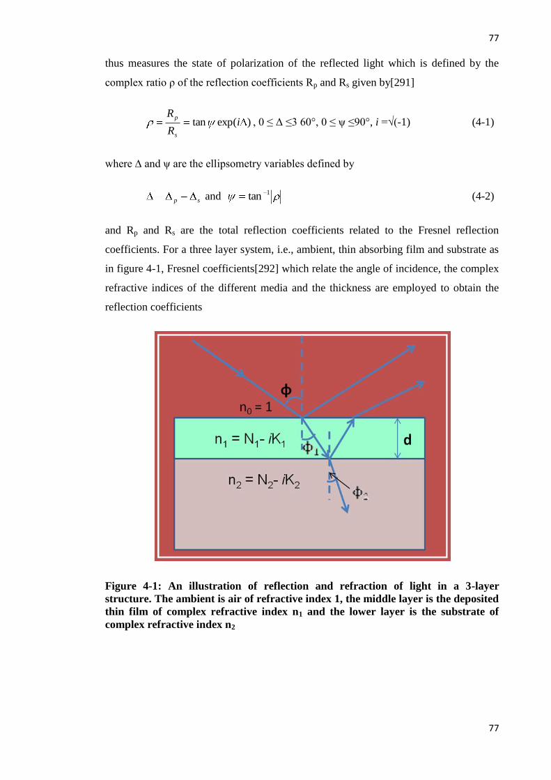
77
77
thus measures the state of polarization of the reflected light which is defined by the
complex ratio ρ of the reflection coefficients Rp and Rs given by[291]
)exp(tan iR
R
s
p, 0 ≤ Δ ≤3 60°, 0 ≤ ψ ≤90°, i =√(-1) (4-1)
where ∆ and ψ are the ellipsometry variables defined by
sp and 1tan (4-2)
and Rp and Rs are the total reflection coefficients related to the Fresnel reflection
coefficients. For a three layer system, i.e., ambient, thin absorbing film and substrate as
in figure 4-1, Fresnel coefficients[292] which relate the angle of incidence, the complex
refractive indices of the different media and the thickness are employed to obtain the
reflection coefficients
Figure 4-1: An illustration of reflection and refraction of light in a 3-layer
structure. The ambient is air of refractive index 1, the middle layer is the deposited
thin film of complex refractive index n1 and the lower layer is the substrate of
complex refractive index n2
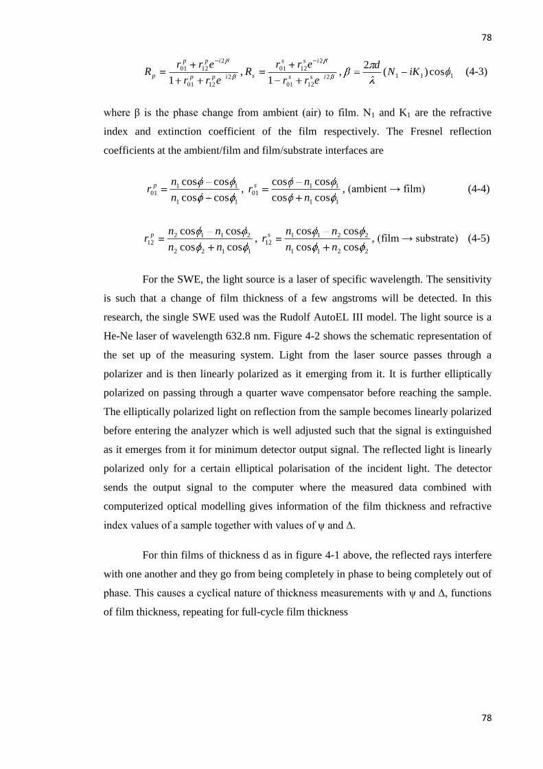
78
78
2
1201
2
1201
1 ipp
ipp
perr
errR ,
2
1201
2
1201
1 iss
iss
serr
errR , 111 cos)(
2iKN
d (4-3)
where β is the phase change from ambient (air) to film. N1 and K1 are the refractive
index and extinction coefficient of the film respectively. The Fresnel reflection
coefficients at the ambient/film and film/substrate interfaces are
11
1101
coscos
coscos
n
nr p ,
11
1101
coscos
coscos
n
nr s , (ambient → film) (4-4)
1122
211212
coscos
coscos
nn
nnr p ,
2211
221112
coscos
coscos
nn
nnr s , (film → substrate) (4-5)
For the SWE, the light source is a laser of specific wavelength. The sensitivity
is such that a change of film thickness of a few angstroms will be detected. In this
research, the single SWE used was the Rudolf AutoEL III model. The light source is a
He-Ne laser of wavelength 632.8 nm. Figure 4-2 shows the schematic representation of
the set up of the measuring system. Light from the laser source passes through a
polarizer and is then linearly polarized as it emerging from it. It is further elliptically
polarized on passing through a quarter wave compensator before reaching the sample.
The elliptically polarized light on reflection from the sample becomes linearly polarized
before entering the analyzer which is well adjusted such that the signal is extinguished
as it emerges from it for minimum detector output signal. The reflected light is linearly
polarized only for a certain elliptical polarisation of the incident light. The detector
sends the output signal to the computer where the measured data combined with
computerized optical modelling gives information of the film thickness and refractive
index values of a sample together with values of ψ and ∆.
For thin films of thickness d as in figure 4-1 above, the reflected rays interfere
with one another and they go from being completely in phase to being completely out of
phase. This causes a cyclical nature of thickness measurements with ψ and ∆, functions
of film thickness, repeating for full-cycle film thickness

79
79
22
1 sin2 nd (4-6)
This appears on the instrument’s panel as “Ord”. Thus the instrument’s reading for
thickness is t for instance, then the thickness of the film could be t+0d, t+d, t+2d,
t+3d,t+4d … t+md, …etc., where m is an integer and d is as defined in equation (6)
which is the value read as “Ord” from the instrument. This therefore requires that one
should have advance knowledge of the film thickness estimate in order to use it for
thickness measurements.
Figure 4-2. Illustration of the layout of a single wavelength ellipsometry (SWE)
Another drawback with this measurement technique is that the equations are
based on macroscopic Maxwell’s equations and on a model that assumes uniform
optical properties with sharp planar film substrate boundaries. Thus results of films of
atomic dimensions become doubtful and questionable. This drawback is however not
relevant in this work since film thicknesses were much larger than atomic dimensions.
4.2.1.2 Step Profilometry
Stylus profilometry is a non-destructive film topology measurement technique
which involves the measurement of a film step topology by mechanical movement of a
diamond needle stylus across the surface of the sample. The resolution of the
measurement is affected by the radius of the stylus and the geometries of the feature on
the measurement surface, the penetration depth and ambient and equipment vibrations.

80
80
The profiler used in this work was the Tenco-alpha step 200 profilometer
equipped with a standard stylus of 12.5 micron radius. It is designed to measure samples
of maximum thickness of 16.5 mm and diameter 162 mm. It can operate in two scan
modes: the kilo angstrom (kÅ) mode with a maximum vertical range of ±160 kÅ and
resolution ±5Å and the micron mode with a maximum range of 160 μm and resolution
±5 nm. Horizontal scan lengths can be set to 40, 80, 2000 or 10,000 μm.
For step height measurements, it is imperative for the sample to have a flat
surface with well defined step in order to generate a good profile. Usual substrates are
silicon wafers or glass slides. In this work, the instrument was used to measure Si,
Si3N4 and NFD film thicknesses. As the measurements require an abrupt step on the
sample under measurement, various techniques exist of creating the step. One of these is
that used by Cross [293] which involves a heavy line of ink from a felt-tip permanent
marker drawn onto the substrate before film deposition. While this technique could be
suitable for some types of films, it was inapplicable in the case of NFD films since it
requires washing off the ink after deposition as this could re-dissolve the NFD coating
in the ethanol solvent. The step was created, in the case of NFD, by only partially (not
wholly) dipping the substrate in the NFD solution during coating but, allowing a clear
clean space above the surface of at least 5 mm. The scanning diamond tip scanned 2000
μm across the step from the clear uncoated side to the coated side, making sure at least
1000μm was within the coated region so as to be able to safely eliminate the surface
tension effects left on the edge of the step during coating. For silicon and nitride films,
the step was created by covering part of the substrate with a clean cover glass during
deposition in the PECVD reactor. After deposition, the cover glass was gently removed
and a step had formed on the substrate. Scanning was done by moving the tip of the
stylus 2000 μm across this step from bare substrate side to film-grown substrate side as
shown in figure 4-3 below.

81
81
The film thickness was obtained from the average step height of the profile on the
screen of the instrument after levelling operations.
4.2.2 Fourier Transform Infrared Spectroscopy (FTIR)
FTIR is a non destructive measurement technique used for the detection of the
vibration modes of molecules in a material. It is an optical technique based on the
absorption and transmission of infrared radiation as it passes through the material
sample being measured. When IR photons of sufficient energy fall on a diatomic
molecule undergoing a change in dipole, the photon energy is absorbed and leads to an
increase in the vibration energy level and consequently to a transition to the next
vibration energy state.
The working of the FTIR is fundamentally based on the Michelson
interferometer which relies on the interference of IR waves. A simplified diagram is
shown in Figure 4. Light (of wavelength 0.7 - 500μm) from an IR source is incident
onto a beam splitter which splits the beam into two equal halves; one part is transmitted
to and reflected from a fixed mirror M2 while the other half is reflected to and reflected
from a movable mirror M1. The reflected beams from these mirrors are recombined by
the beam splitter and are guided to the sample where absorption and transmission takes
place. The transmitted light is then detected by the detector. The light from the source
Figure 4-3: Schematic illustration of the step profilometry showing the direction
in which measurements were performed and the expected step profile
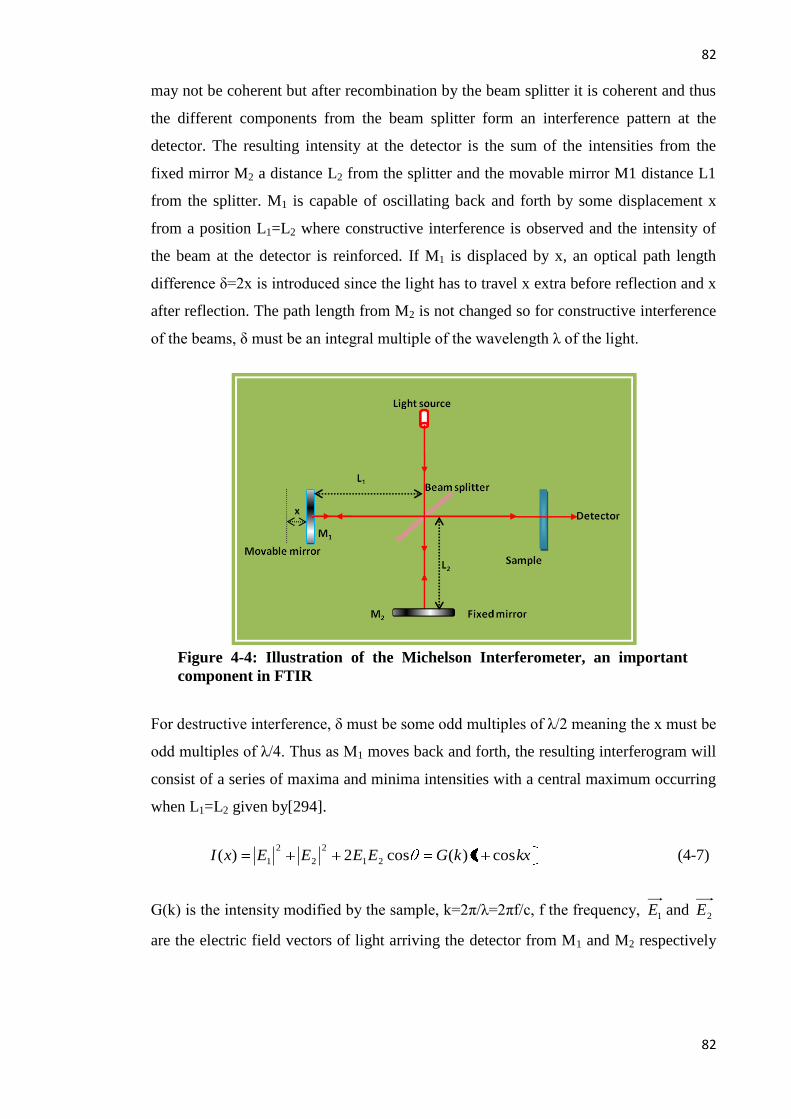
82
82
may not be coherent but after recombination by the beam splitter it is coherent and thus
the different components from the beam splitter form an interference pattern at the
detector. The resulting intensity at the detector is the sum of the intensities from the
fixed mirror M2 a distance L2 from the splitter and the movable mirror M1 distance L1
from the splitter. M1 is capable of oscillating back and forth by some displacement x
from a position L1=L2 where constructive interference is observed and the intensity of
the beam at the detector is reinforced. If M1 is displaced by x, an optical path length
difference δ=2x is introduced since the light has to travel x extra before reflection and x
after reflection. The path length from M2 is not changed so for constructive interference
of the beams, δ must be an integral multiple of the wavelength λ of the light.
For destructive interference, δ must be some odd multiples of λ/2 meaning the x must be
odd multiples of λ/4. Thus as M1 moves back and forth, the resulting interferogram will
consist of a series of maxima and minima intensities with a central maximum occurring
when L1=L2 given by[294].
kxkGEEEExI cos1)(cos2)( 21
2
2
2
1 (4-7)
G(k) is the intensity modified by the sample, k=2π/λ=2πf/c, f the frequency, 1E and 2E
are the electric field vectors of light arriving the detector from M1 and M2 respectively
Figure 4-4: Illustration of the Michelson Interferometer, an important
component in FTIR

83
83
and θ is the phase difference corresponding to the optical path length difference δ. For a
multifrequency emission, the intensity is the integral sum over all frequencies, given by
dkekGI
dkee
kGdkkGdkkxkGxI
ikx
ikxikx
)(2
1)0(
2
1
2)()()cos1)(()(
0 0 0
(4-8)
If equation (8) is multiplied by 22 and rearranged, the familiar Fourier transform
expression is obtained
dkekGIxI
xT ikx)(2
1
2
)0()(2)( (4-9)
The detected intensity as a function of moving mirror position, T(x) can therefore be
converted into the intensity spectrum G(k), as a function of frequency by a simple
Fourier transform
dxexTkG ikx)(2
1)( (4-10)
This transformation is done by the computer. The interferogram has the unique property
that every data point, a function of the movable mirror position, has information about
every IR frequency from the source.
The FTIR instrument used in this experiment was the Shimadzu FTIR
spectrophotometer model FTIR-8300S. The resolution used was ±4 and the wave
number range 400-4000 cm-1
. The samples investigated were NFD coatings, silicon and
silicon nitride films on p-type substrates due to high transparency of the p-type Si wafer
to the radiation. Before measurements, an IR spectrum was first obtained for the bare c-
Si substrate to get the background. This was followed by measurements on the sample
under investigation having films (coatings) deposited on a substrate material from the
same batch as the background material so as to reduce any variation that may arise from
using different backgrounds. Background contributions were automatically subtracted

84
84
from the sample by the computer and thus the final spectrum usually obtained was that
of the films (or coatings) only.
The vibration modes of interest were those corresponding to the dipoles H2O,
C-H, C=O and C-O in NFD; Si-H, Si-H2, Si-H3, Si-OH, Si-O, Si-O2, Si-N and N-H in
silicon and silicon nitride films. Information from the spectra, i.e., different frequencies
corresponding to absorption peaks (transmittance dips) was used in identifying
functional groups in NFD and calculating hydrogen and oxygen content of the silicon
films. The hydrogen content was calculated using the equation[53]
dACH
)(0
0 (4-11)
where Aωo is the proportionality constant at vibration mode (wave number) ωo and
αωo(ω) is the absorption coefficient centred at ωo. The oxygen concentration was
calculated using the equation[291]
1CCox (4-12)
where C1 is the conversion factor of the absorption coefficient α at the vibration mode
ω.
In this work, CH was obtained from the infrared wagging mode (ω0 = 640 cm-1
)
because this mode absorption is proportional to the total hydrogen content of the film
and independent of the bonding configuration[295]. The proportionality constant at this
mode Aωo used was 2.1 x 10¹⁹
cm-2
as obtained by Langford A. et al.,[295]. For oxygen
concentration, the conversion factor used was C1= 3.03x10¹⁷
[291] and the absorption
was considered at the SiO2 vibration mode at ~1100 cm-1
.
4.2.3 Ultra-Violet Visible (UV-Vis) Spectroscopy
UV-Vis spectroscopy is based on the principle that light is attenuated when it
passes through a sample as some of it is absorbed, reflected and scattered. The total
resulting transmittance or reflectance can be used to suitably determine some properties
of the material. The transmittance, T is the percentage of the incident radiant power P0
on the sample that passes through the sample, i.e.,
85
85
0P
PT
(4-13)
P is the transmitted power which is the radiant energy per unit area per unit time that
emerges on the other side of the sample. The photons of energy E greater than the band
gap of the material are strongly absorbed by the material and the absorbed energy is
used to excite the electrons to a higher energy levels or excited states. The expression
relating the transmittance, the relative intensities and the absorption through a thickness
d is given by the Beer-Lambert law
deI
IT
0
(4-14)
where α is the absorption coefficient of a film with thickness d. Thus from (4-14) we
can obtain the frequency dependent absorption coefficient α(λ) to be
Td
ln1
)( (4-15)
The optical band gap of the material is related to the absorption coefficient by the Tauc
relation[296]
)()( g
n EEBE (4-16)
where n is ½ for indirect band material like silicon and 2 for direct band gap material
like ZnO, Eg is the optical band gap, B a constant and E the photon energy (in eV) of the
radiation of wavelength λ given by
1240hc
E (4-17)
h being the Plank’s constant and c the speed of EM waves in vacuum, λ in nm. Si being
an indirect band gap material, equation (16) thus becomes[53]
)()( 2/1
gEEBE
(4-18)

86
86
Thus from a plot 2/1)( E against E, the intercept of the extrapolated straight line section
onto the E-axis gives Eg of the material.
Figure 4-5: Inner view of the UV-Vis spectrophotometer (model: Evolution 300).
The red lines are the beam of light[297]
In this study the double beam UV-Vis spectrophotometer Evolution 300 model
from Thermo Scientific[297] shown in figure 4-5 above was used. This system is PC
controlled via PC VISION software which allows for data collection, storage, recall and
analysis in one convenient programme. The system is a dual-beam spectrophotometer
made up of two light sources that cover the UV-Vis range and extends into the near
infra red range (190-1100nm). These light sources are a Mercury lamp as the primary
reference that allows seamless validation and calibration of the instrument and the
Xenon flash lamp which only comes on during measurements. Next to the source is a
photo-etched slit mechanism and a grating of 1200 lines per mm for splitting light into
its different wavelengths, followed by a series of mirrors to direct the beam of light to a
beam splitter that splits the beam into two; one to the reference cell and the other to the
sample. The emerging beams from the reference and the samples are then directed to

87
87
silicon photodiode detectors. During a wavelength scan, this dual-beam system
measures both P0 and P (the intensities) of the reference and sample respectively and the
detection electronics manipulates these values to produce a spectrum of percentage
transmittance or absorption as a function of wavelength. The format that was often
chosen was the percentage transmittance.
Films for UV-Vis measurements were grown on 2.5 x 2.5 cm corning glass
(Cat. No. 2875-25) cover slips substrates and identical substrates without any grown
films on them were used as references. The reference and samples were held in position
vertically with the plane of the glass perpendicular to the beam of light and in front of
the cell holders by improvised holders because the cell holders were not suitable for the
sample/reference geometries. Results obtained were percentage transmittance against
wavelength. To obtain values of α, the expression
100
%ln
1)(
T
d (4-19)
was used from equation (4-15) above.
4.2.4 Atomic Force Microscopy (AFM)
AFM is part of a broader class of techniques collectively called Scanning Probe
Microscopy (SPM) in which a sharp tip is scanned across a sample at very small
distance to obtain a 2- or 3-D image of the surface at nanometre or better lateral and/or
vertical resolution[291]. Apart from the 3-D visualization capability, AFM also offers
both qualitative and quantitative information on many physical properties of material
surfaces such as surface texture, morphology and particle size. A wide range of particle
sizes can be characterized in the same scan, from 1 nanometre to 8 micrometers. In
addition, the AFM characterization can be done in multiple mediums including ambient
air, controlled environments, and even liquid dispersions. Furthermore, unlike scanning
tunnelling microscopy and scanning electron microscopy that require conducting
surfaces, AFM can examine both insulating and conducting surfaces.
AFM operates by the principle that a force exists between the tip and the
sample when the tip is within atomic distance from the sample. This force depends on

88
88
the nature of the sample, the distance between the prop and the sample, the tip geometry
and the sample surface contamination. Figure 4-6 shows a schematic illustration of the
AFM deflection system and the force against the separation of the tip from the sample
surface.
The instrument basically consists of a sharp tip (prop) of radius a few tens of
nm mounted on a cantilever micro-fabricated from Si or Si3N4 on whose length (10s to
100s of μm) the vertical sensitivity of the instrument depends. The x-and y- resolution
varies from 0.1-1nm while the vertical resolution can be 0.1Å [298]. The cantilever is
connected to a piezo-oscillator. Its motion is detected by a laser beam deflection system
where a laser is reflected from the back of the reflective AFM lever and onto a position-
sensitive detector (PSD).
AFM can operate in a variety of modes; contact mode, non-contact mode, and
tapping mode. Each mode is well suited to the nature of the sample. In the contact
mode, the AFM tip is first brought (manually) close to the sample surface, and then the
scanner makes a final adjustment in tip–sample distance based on a set point determined
by the user. When the tip is in contact with the sample surface through any adsorbed gas
Figure 4-6: Illustration of the beam deflection system of the AFM. A position
sensitive photodiode is used to measure the position of the beam. On the right
is the Force against distance z of probe from the sample surface

89
89
layer, it then scans across the sample under the action of a piezoelectric actuator, by
relative motion between the tip and the sample. A laser beam aimed at the back of the
cantilever–tip assembly reflects off the cantilever surface to a split photodiode (PSD),
which detects the small cantilever deflections. A feedback loop maintains constant tip–
sample separation by moving the scanner in the z-direction to maintain the set-point
deflection, without which the tip would “crash” into the sample with even small
topographic features. The atomic force between the sample and probe can be calculated
by measuring the deflection of the lever, and using Hook’s law F = -kz, where F is the
force, k is the stiffness of the cantilever, and z is the distance the lever is bent.
In non-contact mode a stiff cantilever is oscillated in the attractive regime,
meaning that the tip is quite close to the sample, but not touching it (hence,
“noncontact”). The instrument senses very weak Van der Waal’s forces between the tip
and sample which are quite low, on the order of pN (10 -12
N)[299]. This is so low that
ac detection methods are used to detect these small forces. The detection scheme is
based on measuring changes to the resonant frequency or amplitude of the cantilever.
The resonant frequency is given by[291]
m
kf
2
10 (4-20)
where k is the spring constant and m is the mass of the cantilever. This mode of
operation provides lower resolution than the other two (contact and tapping modes).
In tapping mode also known as intermittent contact mode, the tip is alternately
placed in contact with the sample surface to provide high resolution and then lifted off
the surface to avoid dragging the tip on the sample surface and hence preventing
damage to soft specimens and avoids the pushing of specimens around on the substrate
[300-302]. In this mode, the AFM tip–cantilever assembly oscillates near its resonant
frequency at the sample surface while the tip is scanned; thus, the tip lightly taps the
sample surface while rastering and only touches the sample at the bottom of each
oscillation. The frequency at which the vertically oscillating tip alternately touches the
surface and lifts off is generally in the range 50-500 Hz[291]. The intermittent contact
of the tip with the surface causes energy loss which results in reduced amplitude. This

90
90
reduction in oscillation amplitude is then used in identifying and measuring surface
features. This mode of operation is most beneficial to soft, adhesive or fragile samples,
allowing high resolution topographic images of sample surfaces easily damaged by
using the other modes.
In this research, the XE-100 Advanced Scanning Probe Microscope PSIA
model was used for AFM imaging. The non-contact mode was used in other not to
damage the tips of the AFM. No special preparation of samples was needed. Samples
imaged were grown on Si substrates. Information gathered from the surface topography
and phase micrographs were used to obtain surface roughness, differentiate between
amorphous and polycrystalline films and identify grain boundaries between crystals.
4.3 Electrical Characterisation
Through electrical measurements, important properties of silicon and dielectric
films such as photosensitivity, defect density, carrier doping, etc., can be determined as
well as important device properties such as charge storage for MIS devices, carrier
mobility and transistor stability for thin-film transistors and retention and endurance for
memory devices.
4.3.1 Dark- and Photoconductivity
Conductivity depends on a number of factors: in semiconductors for instance, it
increases with increase in temperature; in crystals, it is affected by the crystalline type
and structure because the electronic structure is inherently tied to the crystal structure;
in polycrystalline materials, the grain size of crystallites and grain boundaries affect the
scattering of carriers[294].
Photoconductivity is the increase in electrical conductivity of a semiconductor
or insulator caused by the excitation of additional free charge carriers when the material
is exposed to photons of sufficiently high energy. The electrical conduction of a
semiconductor or insulator in the absence of radiant energy (in the dark) is known as
dark conductivity. The ratio of dark to photoconductivity defines an important figure of
merit known as photosensitivity. For device quality a-Si:H, dark conductivity is in the
order of 10-9
-10-11
Ω cm-1
while the photosensitivity is in order of 104-10
6. In crystalline

91
91
material and polycrystalline material the conductivity is much higher thus rendering
photosensitivity to be lower ~ 100. Photoconductivity includes the generation and
recombination of charge carriers and obviously their transport to the electrodes. This
means that the thermal and hot carrier relaxation processes, charge carrier statistics and
the many recombination mechanisms are involved in photoconduction. Each of these
processes and each recombination mechanism are complex, which in turn makes
photoconductivity a very complex process to describe[303]. In spite of the complexity,
it provides very valuable information about the physical properties of a material.
Though a complex process, a simplified explanation of photoconductivity can
be given. When a material is irradiated with light of photon energy greater than the band
gap of the material, this leads to the creation of free charge carriers in the conduction
and valence band. These excess charge carriers appear in the external circuit as an
increase in electrical conductivity of the semiconductor material. Photon energy slightly
less than the band gap of a semiconductor material can also create charge carriers. This
is the case in doped semiconductors in which the impurity atom absorbs the photon and
creates free electron in the conduction band. Furthermore, when the energy of the
photon equals the ionization energy of the impurity atoms, this causes ionization of the
impurity leading to an increase in conductivity. This type is known as extrinsic
photoconductivity[303]. The band-to band transition in optical absorption and the
creation of free charge carriers can be extended to amorphous semiconductors.
However, the density of states in amorphous semiconductors is greater than in
crystalline semiconductors. This leads to higher optical absorption compared to
crystalline semiconductors thus greater photosensitivity.
Various methods are often used to measure the conductivity of a semiconductor
material. The method used in this work involves measuring current in darkness and
under illumination with a light source across gap-cell aluminium evaporated electrodes
on silicon films on glass substrates. The experimental set up is as shown below. The
gap cells are of four different gap lengths 100, 200, 500 and 1000 microns. By ramping
the voltage across the different gap cells from 0-25V at a voltage step of 0.2V and
measuring the current using the picoammeter, the conductivity across each gap cell can
be obtained using the equation
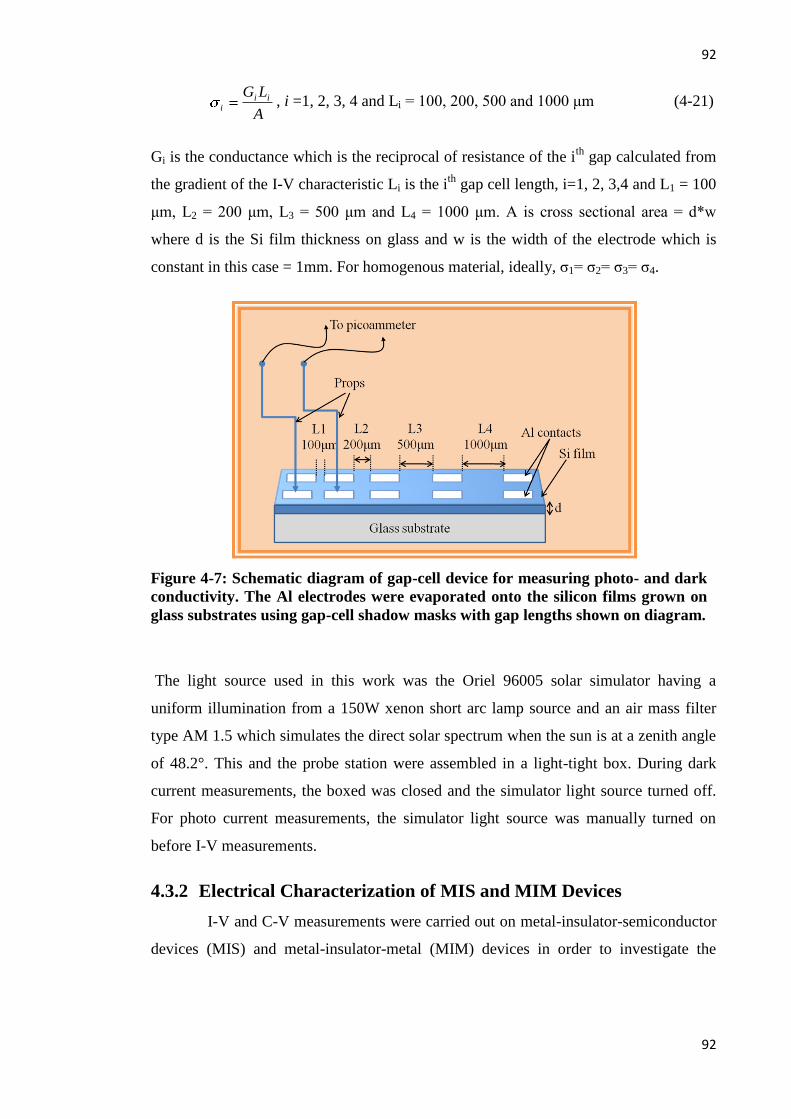
92
92
A
LG ii
i, i =1, 2, 3, 4 and Li = 100, 200, 500 and 1000 μm (4-21)
Gi is the conductance which is the reciprocal of resistance of the ith
gap calculated from
the gradient of the I-V characteristic Li is the ith
gap cell length, i=1, 2, 3,4 and L1 = 100
μm, L2 = 200 μm, L3 = 500 μm and L4 = 1000 μm. A is cross sectional area = d*w
where d is the Si film thickness on glass and w is the width of the electrode which is
constant in this case = 1mm. For homogenous material, ideally, σ1= σ2= σ3= σ4.
The light source used in this work was the Oriel 96005 solar simulator having a
uniform illumination from a 150W xenon short arc lamp source and an air mass filter
type AM 1.5 which simulates the direct solar spectrum when the sun is at a zenith angle
of 48.2°. This and the probe station were assembled in a light-tight box. During dark
current measurements, the boxed was closed and the simulator light source turned off.
For photo current measurements, the simulator light source was manually turned on
before I-V measurements.
4.3.2 Electrical Characterization of MIS and MIM Devices
I-V and C-V measurements were carried out on metal-insulator-semiconductor
devices (MIS) and metal-insulator-metal (MIM) devices in order to investigate the
Figure 4-7: Schematic diagram of gap-cell device for measuring photo- and dark
conductivity. The Al electrodes were evaporated onto the silicon films grown on
glass substrates using gap-cell shadow masks with gap lengths shown on diagram.

93
93
quality and suitability of the material as charge storage medium in the case of MIS and
memory performance (retention and endurance) in the case of MIM devices. All I-V
measurements were performed using an HP 4140B picoammeter and the capacitance
measurements (C-V, C-T) were performed with the HP 4192A LCR bridge. The
minimum measureable current with the picoammeter is 1 pA. HP 4192A is an
impedance analyzer with a frequency range of 5 Hz to 13 MHz and voltage range of -
35V to 35V and capacitance measuring range of 0.1fF to 199 mF.
The probe station was enclosed in a an electromagnetic radiation shielding
metal box. This was necessary in order to minimize the effect of light and other external
influences on measurements as well as provide electromagnetic shielding. The set up
was as shown in the diagram below.
Prior to every C-V measurements of a device, the leakage current was first
measured by ramping voltages from -5V to 5V. Only devices with leakage currents less
than 10 nF proceeded to C-V measurement. C-V data were purposely used to analyse
charge storage in films grown.
4.4 Summary
In this chapter, the various techniques for characterizing the silicon films and
other materials grown in this work have been analysed. It has been shown that the films
grown and the NFD coating thicknesses were measured using either ellipsometry or step
Figure 4-8: Set up of the electrical measurement system

94
94
profilometry. Optical characterization was done by UV-Vis spectroscopy from which
results were used to determine the band gap which is an important electronic property of
materials. Structural characterization by means of AFM has also been discussed.
Furthermore, the way information about the bonding configuration and the different
vibrational modes of Si-H bonds in Si films and COO and C-H in NFD were obtained
through FTIR spectroscopy has also been discussed. Additionally, electrical
characterizations that include conductivity measurements as well as capacitance
measurements have also been discussed. It is through these characterization techniques
that an evaluation can be made of the quality and type of material grown using this
novel technique, assess the performance of device fabricated with the silicon films
grown by the novel low temperature technique and investigate the possible effects of the
low thermal growth technique on the performance of memory devices.

95
95
Chapter 5. Dip-Coating and FTIR Investigation
of Nickel Formate dihydrate
5.1 Introduction
Interest in the synthesis and use of ultrafine-sized particles and clusters is
growing because they represent a potentially fertile field in materials science. Among
these are nickel particles and powders which have found a lot of industrial applications
because of their utility and lower cost in comparison to other noble metals like
palladium and silver. Common industrial applications include magnetic recording
media, chemical catalysts and as electrodes in electronic products such as multilayer
ceramic batteries[304]. Ni ultrafine particle-based catalysts have also been
reported[305]. In recent years, Ni nanoparticles have been investigated and proved to be
very successful for catalytic growth of carbon nanotubes [306-308]. Furthermore, Ni
has also been found attractive for metal-induced crystallization (MIC) and lateral
crystallization (MILC) [270, 271, 309-311] of a-Si processes to obtain Polycrystalline
silicon.
Various precursors and processes have been used to synthesise the ultrafine
particles of Ni. These include nickel nitrate[312] and NiCl2[313] by spray pyrolysis;
amine complexes formed from NiCl2, aqueous NH3 and ammonium bicarbonate[314]
by ultrasonic spray pyrolysis; the decomposition of nickel formate on sol-gel
alumina[315], de-oxidation of Ni(OH)2 with ethylene glycol by polyol method[316],
chemical reduction of aqueous salt NiCl2.6H2O[305] and so on. The widely used Ni
nitrate precursors first decompose to NiO in the calcinations process[317].
Because of the detrimental effects of oxides on the electronic properties of
Polycrystalline silicon films, the use of nitrate as precursor for the metallic Ni as
seeding material for silicon structures is not beneficial. Furthermore, using spray
pyrolysis, the minimum furnace set temperatures for complete reduction to metallic Ni
410-550°C from the nitrate precursors[312], which is considerably high temperature
where plastic substrates are required. On the other hand, NFD precursor is found to
readily decompose to Ni metal at less than 300 C[318]. This makes this precursor more

96
96
preferable compared with the others. While spray pyrolysis is an excellent method of
preparing fine particles and films on substrates because of the high quality of the
product[319, 320], it is not well-suited for this work where there is need for reduction of
process steps. Dip-coating is more advantageous because of the possibility to control the
quality of the final product by controlling the dip-coating parameters as well as the
concentration of the solution.
In this chapter, key processes in the preparatory steps leading to the production
of the Ni seeding material from NFD precursor for the growth of Polycrystalline silicon
are described in detail. This shall include discussion of the basic properties of NFD,
some process routes of NFD, experiments leading to the selection of suitable solvent for
the NFD, the preparatory steps of the substrates for dip-coating, the dip-coating process,
and some explanations of observed results from the dip-coating. Furthermore, the
chapter includes FTIR studies of coated NFD on p-type silicon wafers and the effect of
thermal treatment of this compound through calcinations in the PECVD reactor at high
vacuum. The essence of the FTIR study is to confirm results about the NFD widely
found in literature and to have an advanced knowledge of what could be expected when
the compound is subsequently used in the growth of Polycrystalline silicon in the RF-
PECVD reactor. The chapter ends with a summary of what has been discussed and
importantly the optimum conditions selected for coating NFD on substrates glass and
silicon wafer.
5.2 Basic Properties of Nickel Formate Dihydrate
Nickel formate dihydrate (NFD) is a nickel salt with the chemical formula
Ni(HCOO)2.2H2O having a molecular weight of 184.7. It is a powder, green-turquoise
in colour and sparingly soluble in water. Its structure is as shown in the figure below.
On heating, the compound decomposes in two steps to metallic Ni with the
simultaneous evolution of carbon monoxide and carbon dioxide[321]
Ni(HCOO)2.2H2O → Ni(HCOO)2 + 2H2O (1) Dehydration

97
97
Ni(HCOO)2 → Ni + H2 + 2CO2 (2a) Decomposition
Ni(HCOO)2 → Ni + H2O + CO + CO2 (2b) Decomposition
Fox et al[321] have found through thermo gravimetric studies the activation
energies for dehydration and decomposition to be 25.3±2.0 and 33.1±3.0 kcal. mol-1
respectively. Differential scanning calorimetry (DSC) and thermo gravimetric analysis
studies have found that dehydration of the salt occurs at ~ 150-260°C while
decomposition into metallic Ni occurs at ~ 260-290°C[315, 321, 322].
5.3 Dip-Coating of NFD
Ni nanoparticles and powders have been obtained from NFD and other
precursors through various ways. These include squirting [306, 308, 323] wherein the
solution of the precursor is squirted onto a substrate and allowed to evaporate. Whilst
simple, the difficulty to control film uniformity and thickness makes it inappropriate for
use in situations where the film uniformity is critical in determining the electrical
properties of materials or devices. Another such method is chemical spray pyrolysis
[312, 322].
Chemical spray pyrolysis has for many decades been one of the major
techniques of depositing thin film materials on large area substrates. In this deposition
technique, a solution of the precursor is pulverized by means of a neutral gas so that it
arrives at the substrate in fine droplets. The chemical reactants in the precursor solution
are selected in a way that the by-products other than the final desired product are
volatile at the deposition temperature[324]. The equipment is simple, operation
temperatures are low (100-500°C) and films homogeneity, thickness and smoothness
can be controlled by the spray parameters[324, 325].
However, the dip-coating technique is a much simpler technique when
compared with spray pyrolysis and the coating is performed at much lower temperatures
(< 150°C) with a range of deposition variables to control the morphology of the final
film. The technique has many factors that contribute to the final state of the dip coated
thin film. By controlling the functionalization of the initial substrate surface,
submersion time, withdrawal speed, number of dipping cycles, solution composition,

98
98
concentration and temperature, number of solutions in each dipping sequence and
environment humidity, a large variety of repeatable dip coated film structures and
thicknesses can be fabricated. The technique is capable of providing coatings with
uniform, high quality films even on bulky and complex shapes[326].
5.3.1 The Nima Dip-Coater System
The Dip-coater used in this work is the 4-vessel Nima Precision Dip Coater
with a DC motor controlled carousel shown in figure 5-1 on which the four glass vessels
(150ml each) are lined. These vessels could be used for cleaning, for multiple solution
deposition cycles or for rinse sequences. The vessels used were double-walled and
connected to each other by rubber tubing that are connected to and from a temperature
controller which circulates warm water between the inner and outer walls of the vessels.
Figure 5-1: An illustration of the Nima precision dip-coater system.
The content of the vessel is maintained at a constant temperature which is
controlled by the temperature controller. The vertical dipper arm onto which the
substrate holder is attached is DC motor controlled and can provide smooth vertical
linear motion of the substrate and holder at all dipping speeds from as low as 1
millimetre per minute. Two removable holders were available for use; the single
substrate holder and the multiple substrate holder. The removable holder is attached to

99
99
the movable arm by a magnetic knob. The dipper system is pc-controlled via an IU4
interface unit. The software used is LabVIEW and the control deposition features
include setting the upper and lower substrate resting positions (Raise to and lower to (in
mm)), immersion speed (Down Speed (mm/min)), submersion period (Wait at bottom
(s)), withdrawal speed (Up Speed (mm/min)), drying period (Wait at top (s)), number of
dip cycles and solution holder rotation sequence for multiple solution depositions. The
entire setup was on a workbench inside a wet bench in a clean room under controlled
atmospheric conditions. The settings are necessary in order that toxic fumes from the
precursor solution are safely evacuated via the hood.
5.3.2 Preparation of Precursor Solution
In order to prepare the precursor solution that would produce good results, it
was important to choose the best solvent for the green NFD salt obtained from Alfa
Aesa. The salt was used without further treatment. Since the final film from this
solution would be used to grow silicon structures for electronic devices, it was
necessary that the final solvent would not have a major impact on the electronic
properties of the silicon films obtained through the use of this catalyst. Geng et al.,[323]
had used an alcohol to dissolve the NFD salt for the growth of carbon nanotube.
Trial dissolution of the salt in methanol and ethanol produced identical results
and so methanol was chosen among the two alcohols. Equal volumes of water and
methanol were used to produce separate solutions of 1-10 mg ml-1
of solutions. The
volume of solution produced in each case was 50 ml. This was done by weighing an
appropriate amount of salt in a vial using a digital balance and transferring the measured
salt into another container into which an appropriate amount of solvent was added using
a pipette. The water solvent used was 18 MΩ resistant deionised (DI) water. The binary
mixture of methanol and NFD salt or DI water and NFD salt were left to dissolve in an
ultrasonic bath.
It was observed that, for concentrations of 1-5 mg ml-1
of salt in either water or
methanol, a clear green solution was formed within 10 hours of ultrasonication in an
ultrasonic bath. For 10 mg ml-1
of salt in methanol, a milky green mixture was obtained
and part of salt recrystallized after being kept for some hours undisturbed. However, for

100
100
concentrations of 10 to 30 mg ml-1
of salt in water, a solution was formed although it
could take up to 30 hours of ultrasonication for higher concentrations. From these
observations, it was easy to decide the concentrations of salts in the different solvents to
proceed with in the experiments. For methanol, up to 5 mg ml-1
solution was possible
although the 5 mg ml-1
soon turned into a precipitate after a single use. Up to 30 mg ml-1
of solution was possible for water. Above these respective concentrations, it was
difficult to obtain a sustainable solution, i.e. a solution that would not recrystallize or
will not go into a precipitate at least within 1 day when kept undisturbed for after the
solution is formed.
5.3.3 Choosing the Better Solvent
After choosing the right concentrations, the next task was to choose which
solvent would be most suitable to carry on with in the project. In order to make a well
informed decision in this case, the NFD in the respective solvent film-forming
capabilities on glass and silicon substrates as well as their effect on silicon films grown
using NFD coatings from the respective solutions were to guide the choice. As far as the
coatings on the substrates were concerned, different deposition methods were used.
These were spin-coating, squirting and complete immersion coating.
5.3.3.1 Spin coating
The spin coating technique has been used over decades as a means to deposit
thin films of resins, photoresists and organic materials on substrates. The spin-coating
process involves depositing small droplets of fluid at the centre of a substrate then
spinning the substrate at high speeds. Centripetal acceleration causes the droplets to
spread on the substrate thereby forming a thin film of the material on the substrate. The
final thickness and other film properties depend on the properties of the solution from
which the film is formed, the environmental conditions and on the spinning process
parameters. The solution properties here include the viscosity, volatility, percentage
solid and surface tension. The spinning process parameters include the acceleration and
the final spinning speed.
The solutions for spinning were of identical concentrations for NFD in
methanol and DI water. The same spin speed and substrates dimensions of were adopted

101
101
The spinning was carried out under identical clean room conditions on a workbench in
an extracted bench.
The difficulty encountered with the spinning technique was that most of the
solvent was thrown off the substrates and the film formed was patchy and not
repeatable. Even though the methanol solvent dried off faster than water because it is
more volatile than water, identical problems were encountered with the final films.
5.3.3.2 Squirting
Squirting also known as drop coating is another technique of forming films
from liquid solutions. A drop of the solution is squeezed from a tube or syringe and the
fluid lands on a substrate in jets and it spreads on the substrate, and the solvent dries off
leaving a thin film on the substrate. The thickness and other properties of the film
formed depend on the wettability, volatility, viscosity and surface tension of the
solution and also on the environmental conditions.
A syringe was used in this work to pump the solution onto the substrates. It
was observed that jets of fluid that landed on the substrates formed spherical droplets
and did not easily wet the surface. The effect was more pronounced for water. As the
solvent evaporated spots of thick films formed on the substrate which thinned off at the
edges of the film. Again, it took a longer time (hours) for the water to completely
evaporate at room temperature in order to form the film. The methanol evaporated in a
couple of minutes. To quicken evaporation for the water solvent, the substrate was
placed on a hot plate at elevated temperature. Different temperatures were experimented
within the range of 30-80°C. This was not necessary for methanol. It was however
observed that films formed at faster evaporation rates were rougher than those formed at
slower evaporation rate for water. Repeatability was also difficult in this case. Because
of the rough and irregular nature of films, the method was found inappropriate for this
project.
5.3.3.3 Complete Submersion Coating
In this technique, the substrate is simply submerged and kept in the solution for
some time, then removed and allowed to dry in air. The film is formed through
adsorption and diffusion process and the final film properties depend on the solution

102
102
properties and the environmental conditions. It is very similar to dip-coating but for the
fact that the automated dipping mechanism is absent.
In this work, the substrates were kept submerged in the solution, lying
horizontally on the base of the beaker and kept for 20 min. They were then gently
removed from the beakers using tweezers and placed horizontally on a flat surface, then
allowed to dry in air. As usual, those from the NFD-methanol solution dried up in a
couple of minutes while it took a much longer time for those from NFD-water solution
to dry up and form the film. However, films from this method were more uniform and
repeatable as long as the same concentration was used and the drying surfaces were of
identical geometry. It was also difficult to measure the thickness of the film.
Ellipsometry proved difficult because the incident laser beam on the film surface was
scattered through many angles and thus the reflected beam could not reach the analyser.
It is after this method that the dip coating method was used to later optimize
film thicknesses. Among the three methods discussed the complete submerged method
was adopted to coat NFD on glass substrates that were subsequently used to grow
silicon films
Films were grown in the PECVD reactor previously described in chapter 3 at
growth conditions of reactor chamber pressure 150 mtorr, silane flow rate of 50
standard cubic centimetres per minute (sccm), substrate temperature of 400 °C, and RF
Power of 25W. It must be noted that these deposition conditions were not the optimized
growth conditions in this project but were used in this preliminary part of the project to
isolate the better of two solvents. All substrates prepared with the different
concentrations in the two types of NFD solutions (methanol-solvent and DI water-
solvent) were loaded in the reactor at the same time so that the growth condition would
be identical.
5.3.3.4 Results
At this stage, the Si films grown on substrates coated with NFD dissolved in
methanol and water separately were characterized for optical band gap in order to
observe if firstly, NFD had any effect on the electronic structure of the material formed
and secondly if the type of solvent for the NFD did have any significant effect on the
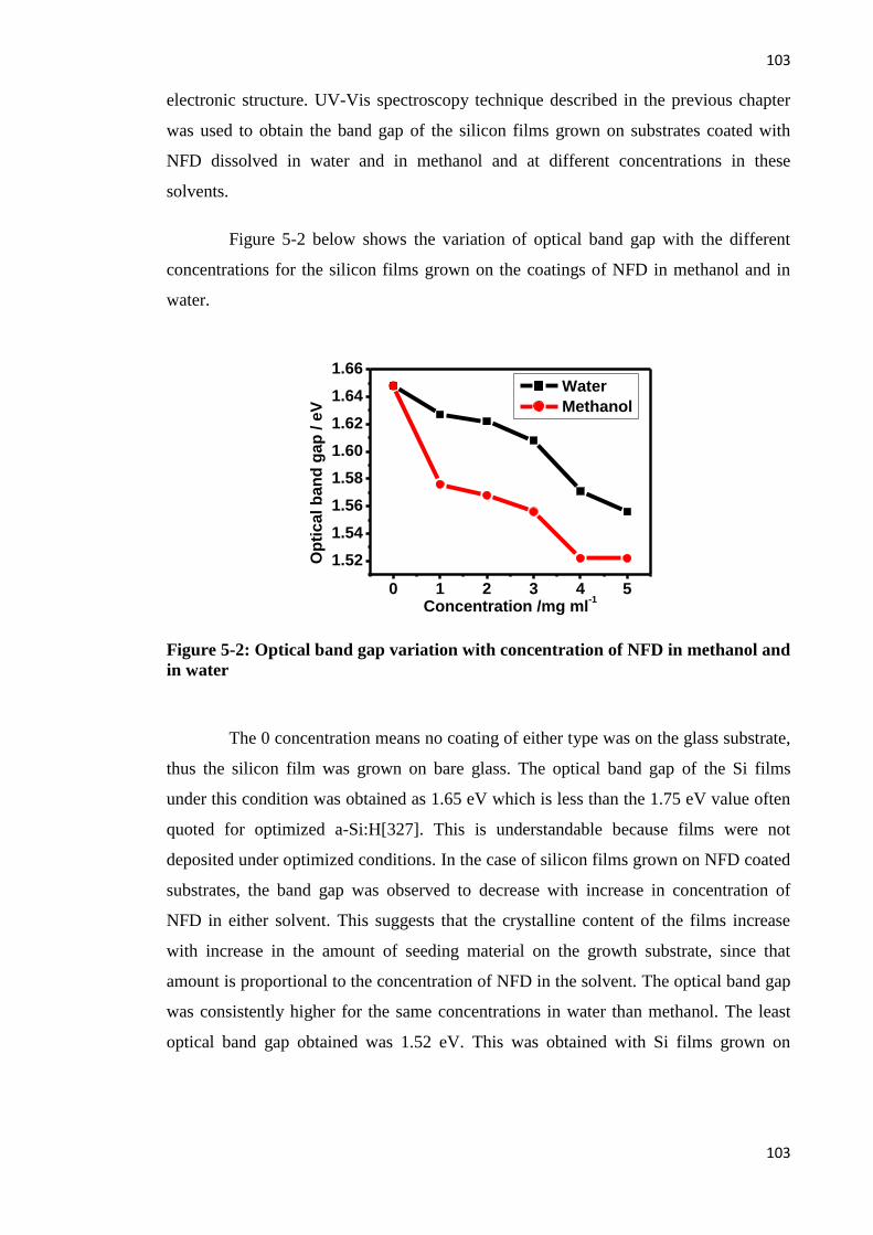
103
103
electronic structure. UV-Vis spectroscopy technique described in the previous chapter
was used to obtain the band gap of the silicon films grown on substrates coated with
NFD dissolved in water and in methanol and at different concentrations in these
solvents.
Figure 5-2 below shows the variation of optical band gap with the different
concentrations for the silicon films grown on the coatings of NFD in methanol and in
water.
0 1 2 3 4 5
1.52
1.54
1.56
1.58
1.60
1.62
1.64
1.66
Op
tical b
an
d g
ap
/ e
V
Concentration /mg ml-1
Water
Methanol
Figure 5-2: Optical band gap variation with concentration of NFD in methanol and
in water
The 0 concentration means no coating of either type was on the glass substrate,
thus the silicon film was grown on bare glass. The optical band gap of the Si films
under this condition was obtained as 1.65 eV which is less than the 1.75 eV value often
quoted for optimized a-Si:H[327]. This is understandable because films were not
deposited under optimized conditions. In the case of silicon films grown on NFD coated
substrates, the band gap was observed to decrease with increase in concentration of
NFD in either solvent. This suggests that the crystalline content of the films increase
with increase in the amount of seeding material on the growth substrate, since that
amount is proportional to the concentration of NFD in the solvent. The optical band gap
was consistently higher for the same concentrations in water than methanol. The least
optical band gap obtained was 1.52 eV. This was obtained with Si films grown on

104
104
methanol-solvent NFD coated substrates. The continuous decrease in the optical band
gap with concentration seemed to suggest that there is an optimal concentration of NFD
for which Si films grown on substrates coated with that concentrated NFD will yield
polycrystalline films with less amorphous phase. However, as observed before,
concentrations greater than 5 mg ml-1
were not possible with methanol, thus attaining
polycrystalline films with close to 0% amorphous phase on the methanol-solvent NFD
coated substrates would be difficult. Given that it is possible to obtain higher
concentrations of NFD in D.I. water and coupled with the fact that the highest
difference in optical band gap for Si films grown water-solvent NFD coated substrates
and methanol-solvent NFD coated substrates was approximately 0.05 eV, DI water was
thus chosen as the better solvent.
Henceforth in the thesis, a solution of NFD will mean that water was used as a
solvent to dissolve the appropriate quantity of the NFD as specified by the concentration
except otherwise specified.
5.4 The Dip Coating Process
After making a choice of the solvent to use, it was now time to optimize the
coating conditions of NFD with the best technique and equipment available. The dip-
coater described above was identified as the best way to coat the material on the glass
and silicon substrates.
To begin with, the substrates were first chemically cleaned following the
cleaning process described in Appendix 1. This process was closely followed by another
cleaning process using argon plasma in a plasma etcher for duration of ~8-10 min at an
RF power of ~80W and pressure of 0.1 mBar as described in Appendix 1. This plasma
cleaning process leads to chemical or organic substances on the substrates to be
selectively broken up and consumed by the high energy plasma, consequently leaving
the substrates smooth and completely freed of the unwanted initial substances and thus
produces the ideal conditions for subsequent coating.
Soon after the substrate cleaning process, one or more substrates were loaded
onto the single or multiple substrate holder of the NIMA precision dip coater described

105
105
above for coating. An appropriate volume of NFD solution was poured into one of the
four vessels connected to a thermal controller. The thermal controller was set to the
required temperature and warm water at that temperature was circulated through the
rubber tubing to the space between the walls of the double-walled vessel. In about 5-10
min, depending on the quantity of NFD solution in the vessel and set temperature, the
solution attained thermal equilibrium with the circulating warm water in the
surrounding jacket. This was confirmed by measuring the temperature of the NFD
solution with a thermometer. Since the NFD vessel was open to the atmosphere, the
temperature controller was usually set to 2-3 °C above the required temperature. When
thermal equilibrium was attained between the NFD solution and the circulating
surrounding water, the substrate was gently immersed into the solution controlled from
a computer with the help of the LabVIEW software in which the dip coater carousel
position and other deposition features such as the upper and lower substrate resting
positions, immersion speed, submersion period, withdrawal speed, drying period and
number of dip cycles had been set.
A complete cycle consisted of lowering the substrate into the NFD solution at a
programmed speed, holding it in the solution for an amount of time herein referred to as
immersion time and withdrawing it at a specified speed and then leaving it to dry in air.
The upper and lower substrate resting position settings control how deep into the vessel
the substrate should go. It did not affect the thickness of the film on the substrate.
However, because the thickness of the films were measured by step profilometry, this
setting was important in creating the step between the substrate and the film. In
addition, number of dipping cycles did not significantly affect the thickness of the
coating because any coating will re-dissolve in the solution the second time it is dipped
into the solution. This was also true of the immersion speed which did not significantly
affect the thickness, but low speeds (~ 10 mm/min) were desired to maintain a still
surface of the solution during dipping. Four main parameters using this system control
the thickness of the NFD coating on the substrates. These are the withdrawal speed, the
immersion time, the temperature of the solution and surrounding and the concentration
of the solution.

106
106
5.4.1 Effect of Immersion Time on the Thickness of NFD Coating on
Substrate
In order to investigate how the immersion time influenced the thickness of
NFD on substrates, it was important to keep all other factors constant while changing
the immersion time and measuring the film thickness. One of the factors capable of
affecting the results is the atmospheric conditions, i.e., humidity, air speed, temperature
pressure, etc. Trying to maintain all these constant in the open atmosphere could prove
very difficult. However, these studies were conducted in a clean room with well
controlled conditions. Thus throughout this investigation, the atmospheric conditions in
the room will be assumed not to vary so much as to affect significantly the results.
The thickness variation studies due to changes in immersion times were
investigated with p-type silicon substrates. Wafers were cut into 2x2 cm2 for the
dipping process. In the dip-coating process, the solution temperature was kept fixed at
30 °C while the withdrawal speed was maintained at 1 mm min-1
. The immersion speed
for this study and all others in this project was constant (10 mm min-1
). The NFD
concentration was first 20 mg ml-1
, and then the experiments were repeated with a
concentration of 30 mg ml-1
. The immersion time, i.e., the time the substrate spent
inside the solution was varied for each dipping cycle and the thickness of the coating
measured using profilometry.
Figure 5-3 shows how the thickness varied for varied immersion times between
5 min and 1 hr. The results showed an increase in thickness with increasing immersion
time. Moreover, the thickness did not increase indefinitely but saturated after some
time. It was further observed that thicker films were obtained with higher concentrated
solutions. This was evident by the fact that the curve for the 30 mg ml-1
solution was
consistently above that of the 20 mg ml-1
solution.

107
107
0 10 20 30 40 50 60
80
120
160
200
240
280
320
360
Solution temperature = 30 oC
Th
ick
ne
ss
/ n
m
Immersion time / min
30 mg ml-1
20 mg ml-1
Figure 5-3: Variation of NFD coating thickness with immersion time for 20 and 30
mg ml-1
NFD solutions each at 30 °C. The withdrawal speed was 1 mm min-1
.
5.4.2 Variation of Thickness with Withdrawal Speed
In this investigation, all other parameters were kept constant except the
withdrawal speed. The temperature of the solution was kept at 30 °C while the
immersion time was 5 min for the 20 mg ml-1
concentration solution. The withdrawal
speed was varied from 1 to 20 mm min-1
in steps of 5 mm min-1
for each dipping cycle.
The thickness of the resulting film was measured at the end of each dipping and the
results were as shown in figure 5-4. It was observed that the film thickness decreased
with increase in withdrawal speed as would be expected.
0 5 10 15 20
50
60
70
80
90
100
Th
ick
ne
ss
/ n
m
Withdrawal speed / mm min-1
20 mg ml-1, T = 30
oC,
Immersion time = 5 min.
Figure 5-4: Thickness variation with withdrawal speed at constant immersion time
of 5 min, solution temperature of 30 °C and concentration of 20 mg ml-1
.

108
108
5.4.3 Variation of Thickness with NFD Solution Temperature
The effect of temperature on the thickness of NFD coating on silicon substrates
was studied by keeping the withdrawal speed constant at 1 mm min-1
, immersion time at
5 min and with a solution of NFD concentration of 20 mg ml-1
. The temperature was
constant for each dipping cycle but was changed from 20 °C to 50 °C for the different
cycles.
The thickness variation with temperature was as shown in figure 5-5a. The
temperature of the solution was found to have a profound effect not only on the film
thickness but also on the film roughness. The roughness data was obtained from the the
alphastep profilometer over the scanned region into the film and data was averaged for
different scan regions on the film. Films were also found to be rougher at higher
temperatures than at lower temperatures as shown in figure 5-5b.
Figure 5-5: (a) Thickness variation with temperature and (b) Average roughness
variation with Temperature of NFD solution at constant immersion time of 5 min
and withdrawal speed of 1 mm min-1
.
5.4.4 Discussion on Observed Effects of Coating Parameters on
Thickness of Coating
NFD thickness on the p-type silicon substrate was found to be strongly
dependent on the concentration of the solution, the immersion time of the substrate in
the solution, the temperature of the solution, the withdrawal speed of the substrate from
(a) (b)

109
109
the solution and even the atmospheric condition. In order to minimize atmospheric
effects on the thickness of the coated films it was important to carry out the entire dip-
coating process under clean room conditions so as to properly control the atmospheric
conditions.
From the graph of the variation of thickness and withdrawal speed of the
substrate from a 20 mg ml-1
NFD solution, the thickness of the coated films on the
substrate was observed to decrease with increase in speed. A plausible explanation of
this is that most of the liquid is pulled back to the bulk at high speed to balance the drag
force. This leaves a thinner film on the substrate in comparison to when the withdrawal
speed is low. For extremely low speeds (1 mm min-1
), the effect of gravitational drain is
also minimized as the solvent on the substrate very close the bulk surface of the solution
evaporates before another part is exposed. At higher speeds, a larger wet substrate area
is exposed and gravitational drain also plays a part apart from evaporation in reducing
the thickness of the film. As the study was carried out under clean room conditions at
the same temperature, the evaporation rate was thus fairly constant.
The increase in thickness with temperature can be explained by relating the
effect of temperature on evaporation which in turn affects the concentration of the
solution at the surface-solution interface near the solution-air interface. The higher the
temperature, the higher the evaporation rate of the solvent near the substrate/solution
interface. This leads to an increase in the concentration of NFD in this region and thus
the creation of a density gradient near the substrate. This gradient eventually affects the
adsorption and diffusion of NFD molecules in that more NFD molecules would get
adsorbed onto the substrate and less would diffuse from the substrate at a higher
concentration than at a lower concentration. Thus at higher solution temperature, there
is less diffusion of NFD molecules into the surrounding, relatively-higher solution
concentration and more adsorption onto the surface leading to a higher thickness of the
film.
Regarding the thickness increase with increase in immersion time, adsorption-
diffusion mechanism is thought to be a plausible reason for this observation. Adsorption
dominates early on when the substrate is immersed in the solution giving rise to the
110
110
sharp increase in thickness. As more molecules build up on the surface some diffuse
back into the bulk of the solution. At some point in time, dynamic equilibrium is
eventually attained wherein the rate of adsorption equals the rate of diffusion. This is
evident from the continuous decrease in the rate of change of thickness with immersion
time evident from the flattening of the curve as observed with figure 5-3. At dynamic
equilibrium, the thickness attains a steady state and beyond this immersion time,
thickness no longer changes. For a 20 mg ml-1 NFD solution, the adsorption-diffusion
processes begin to approach dynamic equilibrium after an immersion time of about 40-
50 minutes as seen in figure 5-3. Mathematically, the thickness is observed to follow the
equation
t
eqt edd /, t > to (5-4)
where dt and deq are the thicknesses at immersion times t>t0 and at equilibrium
respectively and τ is a constant time factor which is thought to dependent on the
substrate material or solution type being coated. It is called the immersion time factor
and defined as the immersion time at which the thickness becomes 1/e the maximum
attainable thickness, which is the thickness obtained when diffusion-adsorption attains
steady state. At t = 0, the thickness is d0 measured by immersing the substrate into the
solution and withdrawing it just as it reaches the required depth in the solution reservoir,
i.e. zero programmed immersion time. It cannot be determined from equation (5-4)
except probably after modification of the equation. An analysis of equation (5-4) reveals
that a plot of ln(dt) against 1/t should give a straight line with slope τ and intercept
ln(deq) on the vertical-axis. Following this procedure for the data from the 20 mg ml-1
NFD solution (see figure 5-3), the unknowns from equation (5-4) were obtained and it
was found that the data fits almost perfectly with the experiment. However, the equation
(5-4) is generally valid for t = to where to is the immersion time that would be required
to theoretically obtain the thickness do. From equation (5-4),
)/ln( 0
0dd
teq
(5-5)

111
111
0.02 0.04 0.06 0.08 0.10
5.00
5.05
5.10
5.15
5.20
5.25
5.30
ln(d
/nm
)
1/immersion time [min-1]
Experimental data
Linear fit
0 50 100 150 20060
80
100
120
140
160
180
200
220
Th
ick
ne
ss
/ n
m
Immersion Time / min
Experimental curve
Fitted curve
Figure 5-6: (a) lnd variation with reciprocal of immersion time for experimental
results obtained with the 20 mg ml-1 solution and (b) Thickness variation with
immersion time for experimental and fitted data.
This physically means that theoretical values of thickness at t < to can be
discarded since they do not agree with experiment. This makes sense because although
do is denote as thickness at time t = 0, the substrate actually spends some time
submerged in the fluid which is not accounted for in equation (2) as it is withdrawn at a
very slow speed. For this experiment with the 20 mg ml-1
NFD solution, do was
measured to be 80 nm.
From figure 5-6a, the equilibrium thickness was observed to be ~204 nm and
the immersion time factor τ to be 3.21 min. From equation 5-5, the value of to obtained
was 3.43 min. This reasonably is in agreement with the experiment in which the length
of the substrate submerged in the solution was between 4 and 7 mm and the downward
stroke was 10 mm min-1
and withdrawal speed 1 mm min-1
. Thus, it is reasonable to
readjust immersion time region for which equation (5-4) is valid to be from t ≥ to. Using
these values in equation (5-4), the fitted curve in figure 5-6b was obtained. It is thus
possible to predict with some certainty the thickness that can be obtained after
immersion of the substrate for a given length of time.
5.5 FTIR of Nickel Formate Dihydrate
Having studied the dip-coating of NFD on p-type silicon, cleaned p-type
silicon substrates were then coated with 30 mg ml-1
NFD in solution at 30 C at a down
stroke of 10 mm min-1
and upstroke of 1 mm min-1
and immersion time of 30 min. This

112
112
dip coating condition was found to be the optimal condition that was observed to
produce the best uniform and smooth coatings with thickness between 150-200 nm..
After coating the substrates, some were loaded into the RF-PECVD chamber and
calcined at 250, 300 and 400 °C at high vacuum of pressure 5 mtorr. The calcinations
was performed for 30 min at each temperature after first leaving the substrates in the
reactor for at least 3 hours in vacuum before turning on the heater to heat the substrate
gradually to the required temperature. After calcining, the substrates were allowed to
cool to room temperature before removing from the for FTIR analysis.
0 1000 2000 3000 4000 5000
0.00
0.25
0.50
0.75
1.00
Ab
so
rpti
on
/ a
.u.
Wave number / cm-1
1200 1400 1600 1800 2000
0.00
0.25
0.50
0.75
1.00Asymmetric HC00
-
Symmetric HC00-
Ab
so
rpti
on
/ a
.u.
Wave number / cm-1
as coated
250 oC
300 oC
400 oC
Figure 5-7: FTIR absorption spectra for (a) as-coated NFD on p-type silicon
substrate, and (b) for calcined NFD coated substrates at 250, 300 and 400 °C
showing the formate vibration mode region between 1200 and 2000 cm-1
FTIR measurements were performed on the calcined substrates as well as on
the as-coated substrates. The results were as shown in figure 5-7 above. The absorption
spectra shown in figure 5-8a reveal the formate groups absorption peaks at 778, 1383,
corresponding to the symmetric HCOO- vibration modes, 1580 corresponding to the
asymmetric HCOO- vibration mode, 2890 cm
-1 corresponding to CH vibration mode,
1120 cm-1
corresponding to CHO vibration mode, and the broad peak between 3039-
3677 cm-1
corresponding to H2O mode[328-334]. It was further noticed that after
calcinations at 250 °C and above, the broad peak between 3039-3677 cm-1
was not
found (see figure 5-7b), an indication that the water of crystallization had completely
been lost. All the characteristic peaks of the formate further disappeared after
calcinations at 400 °C. This indicated that the Ni(HCOO)2.2H2O completely thermally
decomposed at 400 °C. Nonetheless, for calcinations at 250 and 300 °C, the symmetric
(a) (b)

113
113
and asymmetric HCOO- vibration modes at 1383 and 1580 respectively were still very
conspicuously present as observed in figure 5-7b. However, the peak intensity was
weaker than in the as-coated sample. It can be inferred that at these temperatures (250
and 300 °C) the Ni(HCOO)2 had not completely decomposed to the metallic Ni. The
results at 250 °C were as expected and corroborate results by Rosenband and Gany
[322] and Fox et al.,[321] who have shown that the formate is not completely
decomposed until at least 295 °C. The presence of the formate group vibration modes
after calcinations at 300 °C could be that the residence time in the reactor at that
temperature was probably not enough for the decomposition to be completed. Another
possible reason could be that the effective substrate temperature was less than 300 °C.
Nonetheless, the complete decomposition at 400 °C shows the material can be used as a
source of seeding material for low temperature growth regime of ≤ 400 °C.
5.6 Summary
In this chapter, detail composition of the NIMA precision dip coating system
has been described. The different trial methods; spin-coating, drop-coating and
complete immersion coating, used in coating the NFD onto glass and silicon substrates
have briefly been described and have been shown not to be good enough to form thick
uniform films of NFD. Systematic studies which lead to DI water being chosen as
solvent for NFD against methanol were also presented. The choice was based on the
fact that higher concentrations could be obtained with DI water as solvent for NFD as
opposed to methanol where the later could only produce a maximum concentration of 5
mg ml-1
compared to 30 mg ml-1
by the former. It has also been shown that four major
coating parameters affect the thickness of the NFD on p-type silicon substrates. These
are concentration of the solution, temperature of the solution, and immersion time
which all lead to increase in thickness of coatings with the respective increase in
parameters while all other factors are held constant, and the withdrawal speed of the
substrate from the solution which leads to a decrease in thickness with its increase. The
major mechanism of coating has been identified as adsorption-diffusion of the NFD
particles in solution onto the substrate and into solution respectively. Furthermore, the
FTIR studies confirmed formate groups in as-coated films on p-type silicon substrates.
After calcinations at 400 °C it was shown that the NFD completely breaks down to
114
114
metallic Ni as no formate vibration peaks were observed. It was also confirmed that
complete dehydration occurs before 250 °C as the vibration modes corresponding to
H2O vanished after calcinations at 250 °C and above. However, results of calcinations at
300 °C were inconclusive. Finally, the optimum coating conditions were found to be as
follows: NFD concentration = 30 mg ml-1
, NFD solution temperature = 30 °C, substrate
immersion speed = 10 mm min-1
, immersion time = 1800 s, withdrawal speed = 1 mm
min-1
. These conditions were arrived at after many varied trial depositions and are found
to produce NFD coatings with fairly uniform and constant thickness of ~ 150-200 nm.
115
115
Chapter 6. Silicon Structures: PECVD Growth
and Optimization
6.1 Introduction
The aim of this chapter is to describe the experimental optimization of silicon
structures grown by the newly developed low temperature technique wherein nickel
formate dihydrate coated onto glass or silicon substrates as described in chapter 5 is
used as a growing surface of silicon films from silane in the RF-PECVD reactor
described in chapter 3 and photographed in Appendix 2. Two sets of materials were
grown; one on uncoated substrates and the other on coated substrates both grown under
identical conditions. Since it is well known that silicon structures grown on bare
substrates in the RF-PECVD at temperatures ≤ 400 °C are mostly amorphous in nature,
the structures on bare substrates will be referred to as amorphous while those grown on
NFD-coated substrates will be referred to as “Polycrystalline silicon”. The silicon films
were deposited from undiluted silane to obtain the a-Si. Most low temperature CVD
process use silane diluted with hydrogen. This high density of hydrogen atoms in the
gas phase causes severe etching of the substrates, resulting to rough topography, low
quality polycrystalline silicon films. Thus was important that undiluted silane be used in
order to be sure that the films obtained on uncoated substrates were a-Si films.
Optimization of the materials was by using sets of conditions deduced from a wide
review of literature as well as from initial characterizations on a large number of trial
depositions. Characterization techniques described in chapter 4 were used to evaluate
the effects of the novel growth technique and the growth process variables on the silicon
films. In the process, parameters were varied in turn while keeping the others constant
and changes in deposited materials properties monitored. Process variables included
substrate temperature, silane flow rate, RF power, pressure, frequency and electrodes
separation. However, throughout the depositions, the frequency and the electrodes
separation were constant at 13.56 MHz and 4 cm respectively. Conclusions about the
nature of the silicon structures grown by this technique were mostly being based on the
comparative study on the properties of films grown on coated and uncoated substrates
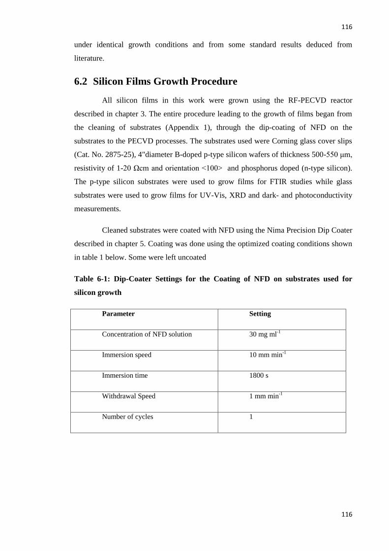
116
116
under identical growth conditions and from some standard results deduced from
literature.
6.2 Silicon Films Growth Procedure
All silicon films in this work were grown using the RF-PECVD reactor
described in chapter 3. The entire procedure leading to the growth of films began from
the cleaning of substrates (Appendix 1), through the dip-coating of NFD on the
substrates to the PECVD processes. The substrates used were Corning glass cover slips
(Cat. No. 2875-25), 4"diameter B-doped p-type silicon wafers of thickness 500-550 μm,
resistivity of 1-20 Ωcm and orientation <100> and phosphorus doped (n-type silicon).
The p-type silicon substrates were used to grow films for FTIR studies while glass
substrates were used to grow films for UV-Vis, XRD and dark- and photoconductivity
measurements.
Cleaned substrates were coated with NFD using the Nima Precision Dip Coater
described in chapter 5. Coating was done using the optimized coating conditions shown
in table 1 below. Some were left uncoated
Table 6-1: Dip-Coater Settings for the Coating of NFD on substrates used for
silicon growth
Parameter Setting
Concentration of NFD solution 30 mg ml-1
Immersion speed 10 mm min-1
Immersion time 1800 s
Withdrawal Speed 1 mm min-1
Number of cycles 1
117
117
NFD coated film thicknesses were in the range 145-200 nm measured using the
Tencor AlphaStep 200 profilometer. The NFD-coated and uncoated substrates were
then loaded into the RF-PECVD reactor. Prior to loading the substrates into the PECVD
reactor, the reactor chamber was plasma-cleaned using CF4 gas at a pressure of 500
mtorr, RF-power of 200 W and at room temperature. The cleaning process lasted for at
least 2 hours, depending on the films previously deposited in the chamber. This process
was necessary in order to reduce the effect of dusty plasma and to avoid foreign
particles and dust being embedded in the new films that might have negative effects on
the quality of films. After loading the substrates into the reactor, the chamber was
evacuated to high vacuum (~5-10 mtorr) for at least three hours (usually it was left in
the reactor overnight). Operating under high vacuum was necessary in order to reduce
the amount of oxygen in the films grown and also as a safety measure because the
pyrophoric nature of SiH4.
Prior to deposition of silicon films, the nitrogen ballast gas was turned on. The
ballast is used in pumps to dilute toxic exhaust gases. The various deposition variables
such as temperature, silane flow rate, RF power and chamber pressure were also
appropriately set. The RF power was set by first adjusting the power range on the RF
generator by switching between two power levels 50 and 500W and then setting the
required pressure as a percentage of the set range by pressing appropriate keys on
microprocessor unit (MPU) panel. The gas flow rate determined by the Tylan 260 mass
flow controller (MFCs) were set using appropriate keys front of the OPT MPU. For
silane, the maximum flow as determine by its MFC was 100 sccm. The required flow
rate was usually entered as a percentage of the MFC value which in this case was 100
sccm. The pressure was set by entering the required value on the MPU. This was
usually done when the source gas silane was already flowing into the chamber through
the shower head. By setting the pressure value, the throttle valve situated between the
pumps and the chamber was automatically adjusted such as to produce the required
pressure in the chamber. The temperature was set on the Honeywell temperature
controller. The maximum temperature allowable for the reactor was 400 °C.
With every parameter set and as soon as the temperature reading on the
Honeywell temperature controller stabilized at the set value, the process was set running

118
118
and the timing was done manually using a digital stop clock. During the deposition, the
system was constantly checked for reflected power which preferably should be zero.
This was adjusted using the RF power matching unit until the value was zero or very
close to zero. The actual reflected power was calculated by multiplying the reading by
the RF power set range and dividing by 10,000. i.e.
000,10
*Re RangeadingRP (6-1)
where RP is the reflected power. In the deposition of silicon films, the range was
usually set to 50W and the reading on the MPU was usually tuned to be as close to zero
as possible and not above 10 in the worst case scenario. Thus the actual reflected power
was usually ≤ 0.05 W. Once the deposition was completed, the system was allowed to
cool down to below 80 °C before the samples were taken out for characterization.
6.3 Effects of Deposition Parameters on Silicon Films
Properties
Four main parameters were varied, i.e., deposition temperature, chamber
pressure, silane flow rate and RF power; and their effects on film properties such as the
optical band gap, the hydrogen content, the photo- and dark conductivity, the growth
rate and the grain size of Polycrystalline silicon crystals were investigated through
methods described in chapter 4. In the subsequent subsections, the effects of varying
these parameters on these film properties are discussed.
6.3.1 Temperature Effects
Substrate temperature has been found to have profound effects on the
microstructure of silicon films [335-338]. The study of the microstructure is inherently
important because other properties of the film such as electrical and optical properties
are determined by the nature of the microstructure. In order to evaluate the effect of
temperature on the films microstructure, films were deposited at four different
temperatures between 250-400 °C. All other parameters were kept constant.
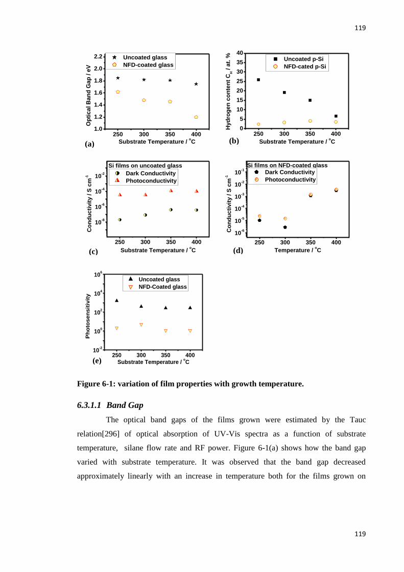
119
119
250 300 350 4001.0
1.2
1.4
1.6
1.8
2.0
2.2
Op
tic
al
Ba
nd
Ga
p /
eV
Substrate Temperature / oC
Uncoated glass
NFD-coated glass
250 300 350 4000
5
10
15
20
25
30
35
40
Hyd
rog
en
co
nte
nt
CH /
at.
%
Substrate Temperature / oC
Uncoated p-Si
NFD-cated p-Si
250 300 350 400
10-8
10-6
10-4
10-2
Si films on uncoated glass
Dark Conductivity
Photoconductivity
Co
nd
ucti
vit
y / S
cm
-1
Substrate Temperature / oC
250 300 350 400
10-6
10-5
10-4
10-3
10-2
10-1
Si films on NFD-coated glass
Co
nd
uc
tivit
y /
S c
m-1
Temperature / oC
Dark Conductivity
Photoconductivity
250 300 350 40010
-2
100
102
104
106
Ph
oto
se
nsit
ivit
y
Substrate Temperature / oC
Uncoated glass
NFD-Coated glass
Figure 6-1: variation of film properties with growth temperature.
6.3.1.1 Band Gap
The optical band gaps of the films grown were estimated by the Tauc
relation[296] of optical absorption of UV-Vis spectra as a function of substrate
temperature, silane flow rate and RF power. Figure 6-1(a) shows how the band gap
varied with substrate temperature. It was observed that the band gap decreased
approximately linearly with an increase in temperature both for the films grown on
(
a)
(
b)
(
c)
(
d)
(
e)
(
e)
(b) (a)
(c) (d)
(e)
120
120
NFD-coated glass substrates and on uncoated substrates. The optical band gaps for the
films grown on uncoated substrates ranged between 1.75-1.95 eV. This range
corresponds to the well known a-Si or a-Si:H optical band gap[327]. Conversely, the
optical band gap of films grown on NFD-coated films was typically in the range 1.6-1.2
eV and decreased with increase in substrate temperature. A decrease in band gap in a-Si
is often attributed to hydrogen evolution[339]. The lower optical band gap for the Si
films on NFD-coated substrates compared with their counterparts on uncoated
substrates suggests that films on NFD-coated substrates are more crystalline [340]. As
would be seen in the proceeding section, the hydrogen content was found to also
decrease with increase in temperature. This thus suggests that at higher deposition
temperatures, more hydrogen was evolved from the films than at low temperatures
leading to a decrease in the hydrogen content of the films and thus the optical band gap
of the material. Moreover, the optical band gap can also be associated with the degree of
disorder in the amorphous matrix. The lower band gap obtained for films on NFD-
coated substrates at the same deposition temperature could suggest that the degree of
disorder is less in the NFD coated films and that a longer range ordering is obtained for
films deposited at higher temperatures. Thus more crystalline structures are obtained at
higher deposition temperatures.
6.3.1.2 Hydrogen Content
Hydrogen incorporation into silicon films and the bonding configuration has a
profound effect on the electronic structure and electrical properties of the films. These
effects can be both beneficial and detrimental. The diffusion of atomic hydrogen in
growing films can be beneficial in that the diffused hydrogen reacts with the silicon
network in the subsurface. This terminates dangling bonds and also breaks and removes
weak Si-Si bonds[53] and thus leads to improved electrical and optical properties of the
material. At too high hydrogen concentration, silicon films show a high density of micro
voids and thus exhibit poor electrical properties[341].
The hydrogen concentration in the a-Si films in atomic percentage was
observed to decrease with increase in substrate temperature (figure 6-1b). This agrees
well with results in the literature [53, 341]. It suggests that more atomic hydrogen is
evolved from the film at higher substrate temperatures than at lower temperatures. Also

121
121
evident is the fact that Si films grown on NFD-coated substrates exhibited very low %
atomic hydrogen compared with their amorphous counterparts and the hydrogen content
was fairly unaffected by the substrate temperature. This suggests that the films on NFD-
coated substrates have less micro voids and the lattice structure is mostly 4-fold
coordinated hydrogen evolution from these films had more to do with the interaction
between the thermal decomposition of nickel formate on the substrate and the silicon
deposition process.
It was also observed that the optical band gap especially of the uncoated films
decreased with decrease in hydrogen content as the temperature increased, suggesting a
dependence of optical band gap on the incorporation of hydrogen in the films. Von
Roedern et. al.[342], suggest that the reason for this is due to the removal of states from
the top of the valence band as hydrogen is being incorporated in the film.
6.3.1.3 Photo- and Dark Conductivity
The variation of photo- and dark conductivity (figures 6-1c and 6-1d) for films
grown on NFD-coated and uncoated p-Si substrates exhibited stark differences. For the
uncoated substrate films, dark conductivity was in the range 10-8
-10-6
S cm-1
and
generally increased with an increase in substrate temperature, while photoconductivity
10-5
-10-4
S cm-1
. For the films deposited on NFD-coated substrates, the dark
conductivity and photoconductivity both range between 10-5
-10-3
and increase with
increase in substrate temperature. It is observed that photosensitivity (figure 6-1e)
which is the ratio of σph to σd ranged between 4 and 2 orders of magnitude for films on
uncoated substrates and 1-0 order for films grown on NFD-coated substrates. Usually, a
high photosensitivity (σph / σd) points to low recombination rate at the mid band gap and
it has been shown that for a transition from amorphous to microcrystalline silicon, the
photosensitivity boundary is around 102
[343]. Thus since all photosensitivity values of
NFD-Coated films are of order101 and 10
0, this suggests that these films have a higher
crystalline content than those grown on uncoated substrates. The increase in
conductivity is also consistent with the hydrogen content and optical band gap results.
As the temperature increases, more hydrogen is liberated from the film and the film also
becomes more crystalline, thus the mobility gap or the separation between the
conduction and valence bands becomes narrower. Charge carriers can thus easily cross

122
122
the gap from valence to conduction band. The higher conductivity observed for NFD-
coated substrate Si films as opposed to uncoated films could also be attributed to
embedded Ni particles in the grown silicon films.
6.3.1.4 Film Surface Roughness and surface grain size
Film surface roughness was studied on AFM topography micrographs for films
grown on NFD-coated and uncoated substrates at various temperatures. Topography
micrographs revealed that average root mean squared (RMS) roughness of surface of
silicon films grown on uncoated substrates were < 1 nm and decreased slightly with
increase in growth temperature while those for the NFD-coated substrates were much
higher > 15 nm for 40 micron length and also decreased with increase in growth
temperature as shown in table 6-2.
Table 6-2: Average roughness of silicon films deposited on NFD-coated and
uncoated p-Si substrates at various temperatures
Growth Temperature Average RMS Roughness of Si films / nm
Uncoated Substrate films NFD-coated substrate Film
250 0.934 48.266
300 0.79 30.694
400 0.715 15.45
This high roughness was obtained because as it would be revealed, grains on
the surface formed in clusters or conglomerates. These conglomerates were not also
uniformly dispersed on the surface and they spiked to different heights. This was
observed for the films on NFD-coated substrates. Figure 6-2 and 6-3, show the surface
topography micrographs of the different film scan. It was possible to observe grains in
different conglomerates on the NFD-coated substrate films when zoomed in as shown in
figure 6-2 and in Appendix 3. However, this was not possible with the films on
uncoated substrates. The grain sizes varied with growth temperature and at different
locations on the surface. The procedure to estimate the surface grain sizes is also shown
in Appendix 3. For the films grown at 250 °C, grain sizes (diameter) varied from 70 nm
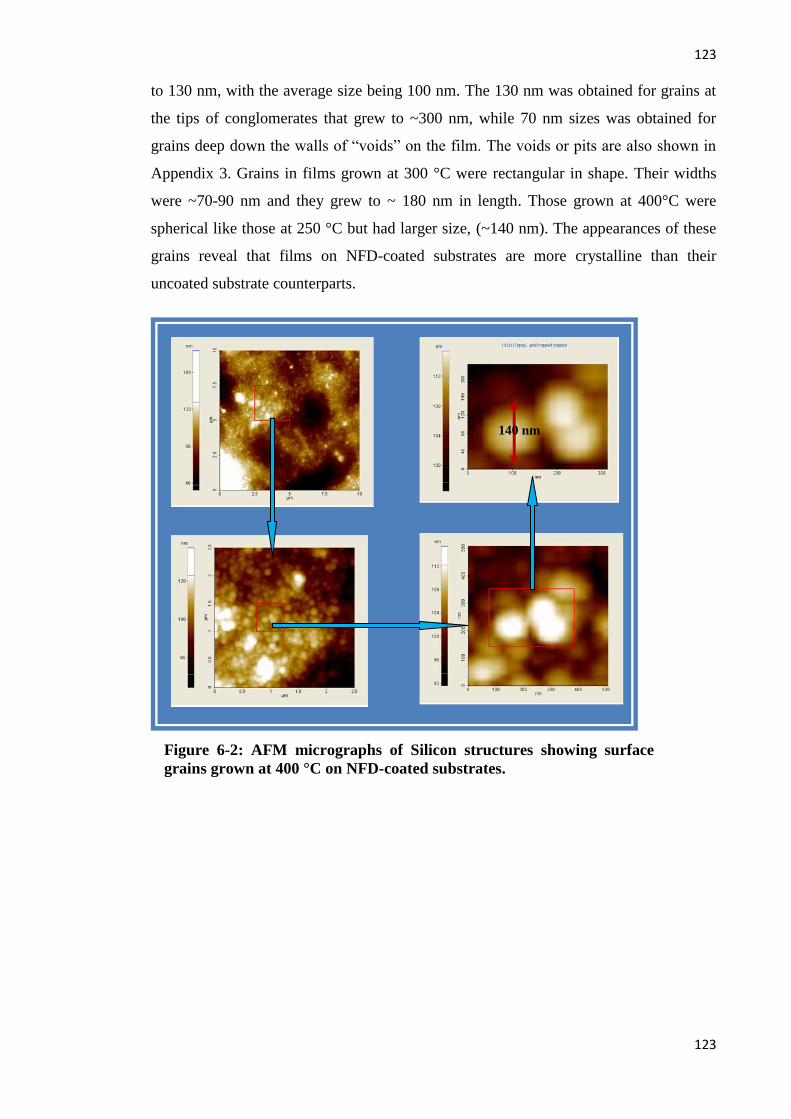
123
123
to 130 nm, with the average size being 100 nm. The 130 nm was obtained for grains at
the tips of conglomerates that grew to ~300 nm, while 70 nm sizes was obtained for
grains deep down the walls of “voids” on the film. The voids or pits are also shown in
Appendix 3. Grains in films grown at 300 °C were rectangular in shape. Their widths
were ~70-90 nm and they grew to ~ 180 nm in length. Those grown at 400°C were
spherical like those at 250 °C but had larger size, (~140 nm). The appearances of these
grains reveal that films on NFD-coated substrates are more crystalline than their
uncoated substrate counterparts.
140 nm
Figure 6-2: AFM micrographs of Silicon structures showing surface
grains grown at 400 °C on NFD-coated substrates.

124
124
Figure 6-3: AFM 3-D topography micrographs showing films grown at different
temperatures. The left column is for micrographs of films on uncoated p-Si
substrates while the right column is for NFD-coated substrates. Rows 1-3 running
from top to bottom are for films grown at 250, 300 and 400 °C respectively.
6.3.2 Effect of RF Power Variation
The RF power applied during each growth controls the rate at which the
precursor gas SiH4 dissociates and thus it is expected to affect the growth rate and the
quality of the film. At low RF powers, the films are expected to have a denser texture
than at high RF power. Film deposition was thus limited in the low RF range (5-25 W)
so as to obtain better quality films even though the RF PECVD system could permit up
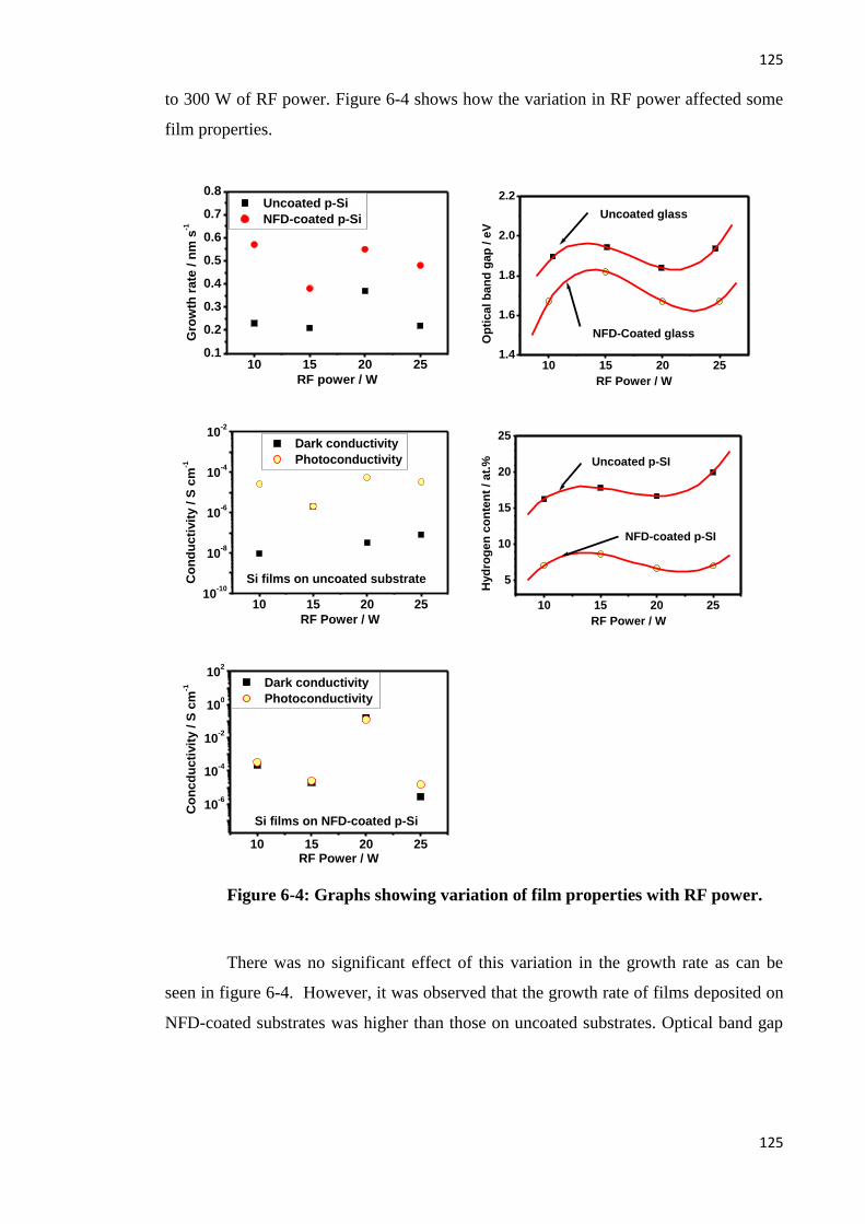
125
125
to 300 W of RF power. Figure 6-4 shows how the variation in RF power affected some
film properties.
10 15 20 250.1
0.2
0.3
0.4
0.5
0.6
0.7
0.8
Gro
wth
rate
/ n
m s
-1
RF power / W
Uncoated p-Si
NFD-coated p-Si
10 15 20 251.4
1.6
1.8
2.0
2.2
NFD-Coated glass
Uncoated glass
Op
tical b
an
d g
ap
/ e
V
RF Power / W
10 15 20 2510
-10
10-8
10-6
10-4
10-2
Si films on uncoated substrate
Co
nd
ucti
vit
y / S
cm
-1
RF Power / W
Dark conductivity
Photoconductivity
10 15 20 25
5
10
15
20
25
NFD-coated p-SI
Uncoated p-SI
Hyd
rog
en
co
nte
nt
/ at.
%
RF Power / W
10 15 20 25
10-6
10-4
10-2
100
102
Si films on NFD-coated p-Si
Co
ncd
ucti
vit
y / S
cm
-1
RF Power / W
Dark conductivity
Photoconductivity
Figure 6-4: Graphs showing variation of film properties with RF power.
There was no significant effect of this variation in the growth rate as can be
seen in figure 6-4. However, it was observed that the growth rate of films deposited on
NFD-coated substrates was higher than those on uncoated substrates. Optical band gap

126
126
and hydrogen content varied in the same manner and was fairly unaffected by the
variation of RF power in the range 10-25W. The identical variation between these two
properties reveals that the electronic structure of the films grown is affected by their
hydrogen content. The higher the hydrogen content, the higher the band gap. This was
observed for both films grown on uncoated and NFD-coated substrates.
The conductivity of the films (both dark- and photoconductivity) was also
relatively unaffected by the change in RF power within the range considered. The
photosensitivity for films grown on uncoated substrates was between 104-10
2 while for
films on uncoated substrates, dark- and photoconductivity were about equal. This again
seems to suggest that the decomposition of the formate is a major contributor in
determining the microstructure of the films.
6.3.3 Effects of Changes in Silane Flow Rate
The rate at which SiH4 was delivered into the reaction chamber was varied
between 10-70 sccm at a constant RF power of 5W, pressure of 200 mtorr and substrate
temperature of 400 °C. The thickness of the films and thus the growth rate was
determined by the deposition time. From figure 6-5, it can be seen that the growth rate
for films on uncoated substrates increases slightly but for the NFD coated substrates, the
growth rate was fairly constant. The growth rate was higher for films on NFD-coated
substrates because the films on these substrates formed on the initially deposited NFD.
The optical band gap, the dark and photoconductivity were also unaffected by the
increase in SiH4 flow rate. However, the hydrogen content of films grown on uncoated
substrates was seen to initially decrease from ~ 12 at.% at 20 sccm to ~ 7 at.% at 35
sccm and remained unchanged thereafter. Meanwhile, for NFD-coated substrates,
hydrogen content was observed to remain constant between 20-50 sccm at ~ 2.5 at. %
but slipped slightly at 70 sccm.

127
127
20 30 40 50 60 70
0.1
0.2
0.3
0.4
Gro
wth
ra
te /
nm
s-1
SiH4 flow rate / sccm
Uncoted p-Si
NFD-coated p-Si
20 30 40 50 60 70
1.2
1.4
1.6
1.8
2.0
2.2
Op
tic
al
ba
nd
ga
p /
eV
SiH4 flow rate / sccm
Uncoated glass
NFD-coated glass
20 30 40 50 60 7010
-12
10-10
10-8
10-6
10-4
Si films on uncoated glass
Co
nd
ucti
vit
y / S
cm
-1
SiH4 flow rate / sccm
Dark conductivity
Photoconductivity
20 30 40 50 60 7010
-10
10-8
10-6
10-4
10-2
100
102
Si films on NFD-coated glass
Co
nd
uc
tivit
y /
S c
m-1
SiH4 flow rate / sccm
Dark conductivity
Photoconductivity
20 30 40 50 60 7010
-2
100
102
104
Ph
oto
sen
sit
ivit
y
SiH4 flow rate / sccm
Uncoated glass
NFD-coated glass
20 30 40 50 60 700
2
4
6
8
10
12
14
Hyd
rog
en
co
nte
nt
CH /
at.
%
SiH4 Flow rate / sccm
Uncoated p-Si
NFD-cated p-Si
Figure 6-5: Variation of film properties with changes in silane flow rate.
6.4 Contamination
Even though only SiH4 was used as the precursor gas for the deposition of
films in the PECVD reactor, FTIR spectra revealed absorption peaks between 1000 -
1200 cm-1
vibration modes which correspond to those of O-Si-O. In previous studies
concerning the vibration spectroscopy of nickel formate, the wave number band 1000-
1400 cm-1
also contained some nickel formate vibration modes, particularly at 1070 –

128
128
1135 cm-1
for the HCO2-, CHO and CO[332]. Careful consideration was thus required to
differentiate whether modes around the band 1000 – 1200 cm-1
could be attributed to
oxygen contamination or the formate groups due to incomplete decomposition of NFD
during the growth process. This was particularly so for films grown on NFD-coated
substrates. The formate modes if present would show a strong absorption peak around
1360 and 1580 cm-1
for HCO2- for the symmetric and asymmetric bending modes
respectively. However, as can be seen in figure 6-6, these modes were absent even for
the devices grown at 250 °C which is below the complete decomposition temperature of
nickel formate. In the previous chapter (Chapter 5, Figure 5-8b), it had been observed
that after baking NFD-coated substrates at 250 and 300 °C, formate modes in the
spectral range 1300-1800 cm-1
were still conspicuously present, except at 400 °C.
800 1000 1200 1400 1600
0
4000
8000
12000
16000
T = 250 oC
Ab
so
rpti
on
co
eff
icie
nt
/ cm
-1
Wavenumber / cm-1
uncoated p-Si
NFD-coated p-Si
800 1000 1200 1400 1600
0
4000
8000
12000
16000
T = 300 oC
Ab
so
rpti
on
co
eff
icie
nt
/ c
m-1
Wavenumber / cm-1
Uncotaed p-Si
NFD-coated p-Si
800 1000 1200 1400 1600-5000
0
5000
10000
15000
20000
25000
T = 350 oC
Ab
so
rpti
on
co
eff
icie
nt
/ cm
-1
Wavenumber / cm-1
Uncoated p-Si
NFD-coated p-Si
800 1000 1200 1400 1600
0
2000
4000
6000
8000
T = 400 oC
Ab
so
rpti
on
co
eff
icie
nt
/ cm
-1
Wavenumber / cm-1
Uncoated p-Si
NFD-coated p-Si
Figure 6-6: FTIR spectra illustrating the effect of film deposition temperature on
the oxygen content of the film. Films were grown at a pressure of 200 mtorr, RF
power of 5W and silane flow rate of 50 sccm.
It is clear from the graphs in figure 6-6 that no absorption peak was obtained at
around the band 1300-1600 cm-1
meaning that the expected usually dominant symmetric

129
129
and asymmetric bending modes of HCO2- were absent. Thus as observed by
Hamelmann et. al.,[344] and a host of others[345, 346], the absorption peak observed at
the spectral range between 900-1200 cm-1
correspond to stretching vibration modes of
O-Si-O and the weak absorption peak observed at ~ 800 cm-1
is the bending mode of
SiO. It is also observed that the asymmetric stretching mode of the O-Si-O is slightly
shifted to the right for the silicon films grown on NFD-coated substrates compared to
their counterparts on uncoated substrates. The right broad shoulder also observed can be
attributed to the asymmetric stretching mode of O-Si-O. This shift in the mode could
actually be due to the formation of siloxane when silane reacts with the organometallic
NFD. The absorption is also observed to be higher for films on NFD-coated substrates
than for the uncoated substrates. Though cautiously attributing the observed effects here
to oxygen contamination, there however is some resemblance between these graphs in
figure 6-6 to the graph in figure 5-9 in chapter 5, meaning there is some reaction
between silane and the partially decomposed formate that affect the composition of the
film.
The concentration of the interstitial oxygen was estimated from N=C1α in cm-3
where α is the absorption coefficient and C1= 3.03x10¹⁷
is the conversion factor of the
absorption coefficient of oxygen in silicon at 300K [291]. The concentration was about
equal for both types of films grown at 400 °C. (1.5-1.6) x 1021
cm-3
while for lower
investigated temperatures, it was it ranged between (1.1-1.6) x 1021
for uncoated
substrate films and (3.6-4.5) x 1021
for NFD-coated substrate films. The source of the
oxygen in the films is not well known and such absorption peaks have been reported in
literature [347-350]. Müllerová et al[349] have suggested that the oxygen could be
introduced due to film exposure to air after growth, while Hiraki[351] has noted an
increase in absorbance around oxygen characteristic peaks with exposure time within
the first 20 hours of exposure and has suggested that the oxygen inclusion in the films is
a diffusion limited reaction. Furthermore, Torres et al., [352] also observed that the
presence of oxygen has a profound adverse effect on the electrical conductivity of the
film and could be responsible for the n-type behaviour of the material. Given that the
PECVD reactor was well evacuated of all air down to a pressure of ~5-10 mtorr, it gives
this author grounds to think that this interstitial oxygen could be due to post deposition

130
130
contamination as a result of exposure of the films to air as well as due to the thermal
decomposition of the formate for the NFD-coated films. This also suggests that the
films are porous and we could actually be obtaining semi-insulating, unintentionally
oxygen-doped Polycrystalline silicon films, resembling those produced by Clough et
al[353].
Another possible contaminant in the films is excess Ni metallic particles. The
possible indication of their presence could be evident in the conductivity of the Si films
grown on the NFD-coated substrates as well as the leakage current in MIS devices
containing these films. As observed, dark conductivity was observed to be within the
range reported in literature and the leakage currents were 101-10
2 times higher than their
counterparts containing a-Si. Nevertheless, these leakage currents remained less than 10
nA, low enough to permit C-V measurements to be performer as would be seen in
Chapter 7. This increase in leakage current could suggest the presence of Ni particles in
the film. Further investigations would be required to establish the presence or absence
of these contaminants in the films.
6.5 Deposition of Silicon Nitride Dielectric
Silicon nitride films used in this work were deposited using the same RF-
PECVD reactor as for the silicon films. As earlier mentioned, these were used as gate
dielectric for memory device. The precursor gases were SiH4 and NH3 with nitrogen as
carrier gas. The independent process parameters that could influence the quality of the
dielectric film deposited were the RF power and the ratio of the flow rate of silane to
ammonia R given by
34/ NHSiH RRR (6-2)
Apart from these parameters, the deposition pressure and the carrier gas (N2)
flow rate and the deposition temperature could also affect the quality of the films.
However, these were kept constant at 350 mtorr, 100 sccm and 300 °C respectively
following semi-optimized conditions in our reactor by Cross [354]. The only significant
changes on these semi-optimized conditions were the gas flow rate ratio of SiH4 to NH3.
This was basically changed by changing the silane flow rate from 5.2 - 20 sccm, leaving

131
131
the flow rate of ammonia constant at 40 sccm. The primary intention here was to reduce
the amount of charge stored in the dielectric so as to easily tell whether charge is stored
in dielectric or in the active silicon film layers sandwiched between the tunnelling layer
and the control gate layer dielectric. This charge stored usually shows up in a
capacitance-voltage graph as a hysteresis and the charge stored is directly proportional
to the hysteresis width. Thus reducing the hysteresis width to an insignificant level was
the intention of this piece of study. It is nonetheless worth mentioning that silicon
nitride is a charge trap-rich dielectric which is often used in SONOS memory devices as
the charge storage medium, and therefore obtaining a hysteresis-free C-V characteristics
could be very difficult. The other properties of this dielectric considered were the
growth rate, the index of refraction (IR) measured by ellipsometry and dielectric
constant obtained from C-V measurements.
Both IR and growth rate were observed to increase with increase in silane to
ammonia flow rate ratio R as shown in figure 6-7.
0.1 0.2 0.3 0.4 0.50.10
0.12
0.14
0.16
Gro
wth
ra
te / n
m s
-1
R = [SiH4]/[NH
3]
0.1 0.2 0.3 0.4 0.5
1.8
1.9
2.0
2.1
2.2
Refr
acti
ve In
dex (
IR)
R = [SiH4]/[NH
3]
Figure 6-7: Variation in growth rate and index of refraction for silicon nitride
films with changes in the ratio R of silane flow rate to ammonia flow rate. Films
were grown at a temperature of 300 °C, RF power of 50W, nitrogen flow of 100
sccm and ammonia flow of 40 sccm while silane flow was changed to change R.
IR varied between 1.83 - 2.05 as R increased from 0.1 to 0.5. This agrees well
with results obtained by Parsons et al[355]. The FTIR spectra of films (figure 6-8) also
revealed that higher absorption N-H peaks at 1150 and 3350 cm-1
were obtained at
lower R (lower silane flow rate) than at higher R. This means films grown at lower R
were nitrogen-richer than at higher R. On the contrary, Si-H peak at ~ 2200 cm-1
decreased with decrease in R. Thus films with higher R are silicon-richer than their
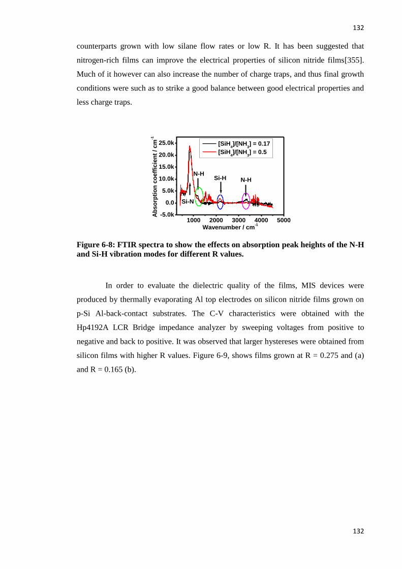
132
132
counterparts grown with low silane flow rates or low R. It has been suggested that
nitrogen-rich films can improve the electrical properties of silicon nitride films[355].
Much of it however can also increase the number of charge traps, and thus final growth
conditions were such as to strike a good balance between good electrical properties and
less charge traps.
1000 2000 3000 4000 5000-5.0k
0.0
5.0k
10.0k
15.0k
20.0k
25.0k
Si-N
Si-H N-HN-H
Ab
so
rpti
on
co
eff
icie
nt
/ cm
-1
Wavenumber / cm-1
[SiH4]/[NH
3] = 0.17
[SiH4]/[NH
3] = 0.5
Figure 6-8: FTIR spectra to show the effects on absorption peak heights of the N-H
and Si-H vibration modes for different R values.
In order to evaluate the dielectric quality of the films, MIS devices were
produced by thermally evaporating Al top electrodes on silicon nitride films grown on
p-Si Al-back-contact substrates. The C-V characteristics were obtained with the
Hp4192A LCR Bridge impedance analyzer by sweeping voltages from positive to
negative and back to positive. It was observed that larger hystereses were obtained from
silicon films with higher R values. Figure 6-9, shows films grown at R = 0.275 and (a)
and R = 0.165 (b).

133
133
-15 -10 -5 0 5
100.0µ
200.0µ
300.0µ
400.0µ
500.0µ
600.0µ
Dielectric constant = 6.16
Al / Si3N
4 / p-Si
4.62 V
Cap
acit
an
ce p
er
un
it a
rea / F
m-2
Gate voltage / V-10 -5 0 5 10
200.0µ
400.0µ
600.0µ
800.0µ
Dielectric constant = 6.45
0.84V
Ca
pa
cit
an
ce
pe
r u
nit
are
a /
F m
-2
Gate voltage
Al/Si3N
4/p-Si
Figure 6-9: C-V curves of Si3N4 MIS for films grown at (a) high silane to ammonia
flow ratio of 0.275 and (b)low silane to ammonia flow ratio of 0.165
These conditions were further improved to reduce the hysteresis width and increase the
dielectric constant. This was done by varying the RF power from 50W to 20W in the
condition of low R (0.165) above. The effect this had on the C-V curves is that the
hysteresis widths were slightly reduced to 0.63V while the dielectric constant improved
significantly to 7.6. Figure 6-10 shows the C-V characteristics and absorption spectra of
the deposition conditions at reduced RF power. This condition of deposition was thus
chosen as the best within the limit of experimental error for use in memory device
fabrication.
-10 -5 0 5 100.0
400.0µ
800.0µ
1.2m
1.6m
Dielectric constant = 7.6
0.63V
Ca
pa
cit
an
ce
pe
r u
nit
are
a /
F m
-2
Gate voltage / V
Al / Si3N
4 / p-Si
0 1000 2000 3000 4000 5000
-0.02
0.00
0.02
0.04
0.06
0.08
N-HN-HCO
2
Si-N
Ab
so
rban
ce (
a.u
)
Wavenumber / cm-1
Figure 6-10: Graphs showing (a) C-V characteristics and (b) FTIR spectra of
silicon nitride films deposited at T = 300 °C, RF power = 20W, SiH4 flow = 6.6
sccm, NH3 flow = 40 sccm, N2 flow = 100 sccm and pressure of 350 mtorr.
(a) (b)
(a) (b)

134
134
6.6 Summary of Chapter 6
In this chapter, the procedure leading to the choice of deposition conditions of
both optimized silicon and silicon nitride films have been discussed. It has been shown
that silicon films grown on NFD-coated substrates show very distinct characteristics
from those grown on uncoated substrates at 250 - 400 °C. The characteristics of the
NFD-coated substrate films resembles more those of poly- or microcrystalline silicon
based on their optical band gaps, hydrogen content and electrical conductivity. The best
films were grown under the conditions which are herein referred to as optimized
conditions shown in table 6-3. Furthermore, silicon nitride films which were used in
memory applications of these silicon films were also optimized and the best growth
conditions are those that resulted to the highest dielectric constant and least hysteresis
width. The conditions are also given in table 6-3.
Table 6-3: Optimized growth conditions of silicon films and silicon nitride films
using the RF-PECVD reactor.
Parameter Value for Si Films
Value for Silicon nitride film
NFD thickness / nm (140 -150)* NA
Temperature / °C 400 300
Pressure / mtorr 200 350
RF Power / W 5 20
Silane Flow / sccm 50 6.6
Ammonia Flow / sccm, NA 40
Nitrogen Flow / sccm NA 100
Optical band gap / eV 1.3*, 1.78
†
Dark Conductivity / S cm-1 ~10-8†
, ~10-5*
Hydrogen content / at.% ~7†, ~3
*
Dielectric constant 7.6
* NFD-coated substrates
† Uncoated substrate

135
135
Chapter 7. Memory Behaviour of NFD-assisted
Grown Silicon Structures
7.1 Introduction
It has been shown in the previous chapter that the silicon structures grown
through the use of NFD coating on the substrates as a source of seeding material and
those grown on bare substrates following conventional PECVD methods exhibit distinct
properties. Some of the results suggest that the structures grown by the novel NFD-
assisted, low thermal budget method are crystalline in nature and their counterparts on
bare substrates are amorphous. Whilst some of these results are encouraging, it is not
enough to assume that this material would be suitable for use as a charge storage
medium in memory devices, particularly in 3-D memory where memory layers are
stacked vertically to increase density.
One of the objectives of this research was to investigate the feasibility of using
this material as a storage medium of information in flash memory. In this chapter
therefore, the investigation of the performance of this material as a charge storage
medium is described. Charge storage and memory effects were investigated by
incorporating the material in the two-terminal devices metal-insulator-semiconductor
(MIS) and metal-insulator-metal (MIM), since they mimic the flash memory cell. This
chapter thus aims at providing the details of the fabrication of the MIS and MIM
devices and the characterization thereafter. Device fabrication will include the
deposition of different insulating materials and the thermal evaporation of metal gates.
Meanwhile, the characterization will mainly be electrical which will include I-V and C-
V measurements as well as capacitance variation with time. All the NFD coatings used
for this investigation are produced under identical optimum conditions stated previously
in chapter 5.
7.2 Fabrication of MIS Devices
All MIS devices were fabricated on boron-doped (p-type) <100> silicon wafers
of resistivity 1-20 Ω-cm with aluminium ohmic back contacts. The substrates were
cleaned as described in Appendices 1 prior to the coating of NFD as described in

136
136
chapter 5. In order to ensure equal thickness of NFD on all devices studied at different
temperatures of PECVD deposition of silicon films, large pieces of the wafer were dip-
coated and cut into suitable sizes, e.g. 1.5 x 4 cm, such that half part of a piece was
coated and part uncoated. This was to ensure that different film types will be deposited
on the same wafer under the same deposition conditions. After coating, the substrates
were loaded into the PECVD reactor that had been cleaned following the cleaning
procedure described in Appendix 1, for film depositions. All films were deposited
following the procedures in chapter 6. The set values of the parameters were 200 mtorr
pressure, 50 sccm silane flow, 5W RF power and the deposition times were adjusted so
as to obtain film thickness of ~ 40 or 100 nm at different deposition temperatures of
250, 300 and 400 °C.
7.2.1 Deposition of Gate Insulator
The deposition of silicon films was usually proceeded by the deposition of an
insulating dielectric layer. In some cases however, especially with the MIM devices, the
deposition of a dielectric (tunnel dielectric) preceded the deposition of the silicon film
followed by another dielectric layer (control dielectric).
Different dielectrics were investigated for possible use as gate insulators. Since
the major objective was to produce a memory device with all processing temperatures ≤
400 °C, it was necessary to carefully choose materials which could be obtained at high
quality at ≤ 400°C. The usual SiO2 was ruled out because PECVD grown SiO2 is
usually not of high quality and added to safety concerns in mixing SiH4 and O2. Those
insulators investigated were zirconium dioxide[356], gadolinium dioxide, silicon nitride
and organic composite insulators polyvinyl acetate (PVAc) and polystyrene (PS)[357].
The choice of these higher dielectrics was due to the fact that as the thickness
of the SiO2 gate dielectric decreases, high leakage current and reduced drive current
becomes fundamental limitations to further scaling of memory devices. Using thicker
dielectric films with higher permittivity than SiO2 could therefore minimize these
problems. Silicon nitride mostly used in this work has the advantage that it is highly
resistant to impurity diffusion and oxidation[358]. ZrO2 was investigated for use but
because the films were grown elsewhere and due to time constraints, the films were not

137
137
included in the device. Likewise gadolinium oxide was also tested but was not
implemented for similar reasons. Thus only silicon nitride and the organic composite
insulator results will be presented here.
7.2.1.1 Polystyrene and Polyvinyl Acetate
Polystyrene (PS)[359] and polyvinyl acetate (PVAc)[360] have been
investigated and found to be good dielectrics for organic electronic devices. A
combination of the two organic dielectrics have been used in organic memory devices
by Paul et al.,[360] and found to produce good results. Furthermore, Kolliopoulou et
al.,[361] have also demonstrated a combination of organic material and silicon in
memory devices. These organic materials offer the advantage of low costs, low
temperature and ease of fabrication (spin-coating).
40 mg ml-1
of PS and 30 mg ml-1
PVAc were prepared separately by dissolving
the organic polymers in dichlorobenzene and methanol solvents respectively and
ultrasonicating in an ultrasonic bath for at least 5 hours until they were completely
dissolved. These were then spin-coated onto the silicon films, first PS then PVAc. The
PS was spin-coated at 4000 rpm and PVAc at 2000 rpm to obtain respective film
thicknesses of 100 nm and 50 nm. The substrates were then left to dry in air and were
ready for the next processing step.
7.2.1.2 Silicon Nitride
Silicon nitride was deposited in the PECVD reactor using the precursor gases
silane, nitrogen and ammonia. The films were deposited at 300 °C chamber
temperature, 350 mtorr pressure, 20 W RF power and silane, ammonia and nitrogen
flow rates of 6.7, 40 and 100 sccm respectively as describe in the previous chapter.
Films were obtained at low growth rate of 5.18 nm min-1
. It should be noted that in most
cases for the final devices analysed, nitride films control insulators were deposited on
the silicon films without breaking vacuum.
7.2.2 Evaporation of Gate Electrodes
Soon as the substrates were removed from the PECVD reactor chamber, they
were loaded into a thermal evaporator Edwards 303. Shadow masks with holes were
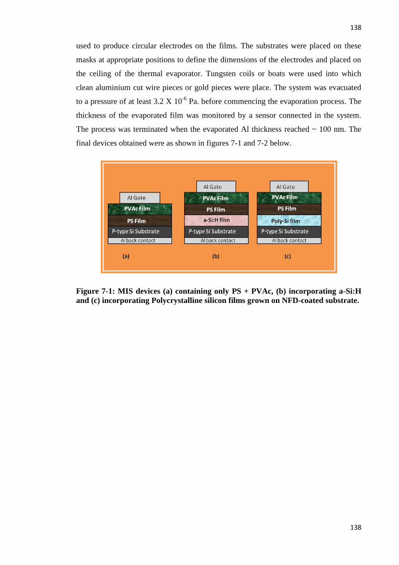
138
138
used to produce circular electrodes on the films. The substrates were placed on these
masks at appropriate positions to define the dimensions of the electrodes and placed on
the ceiling of the thermal evaporator. Tungsten coils or boats were used into which
clean aluminium cut wire pieces or gold pieces were place. The system was evacuated
to a pressure of at least 3.2 X 10⁻⁶
Pa. before commencing the evaporation process. The
thickness of the evaporated film was monitored by a sensor connected in the system.
The process was terminated when the evaporated Al thickness reached ~ 100 nm. The
final devices obtained were as shown in figures 7-1 and 7-2 below.
Figure 7-1: MIS devices (a) containing only PS + PVAc, (b) incorporating a-Si:H
and (c) incorporating Polycrystalline silicon films grown on NFD-coated substrate.
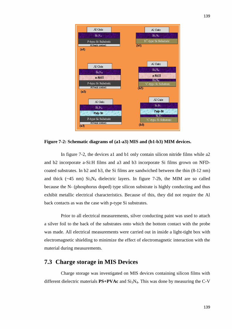
139
139
Figure 7-2: Schematic diagrams of (a1-a3) MIS and (b1-b3) MIM devices.
In figure 7-2, the devices a1 and b1 only contain silicon nitride films while a2
and b2 incorporate a-Si:H films and a3 and b3 incorporate Si films grown on NFD-
coated substrates. In b2 and b3, the Si films are sandwiched between the thin (8-12 nm)
and thick (~45 nm) Si3N4 dielectric layers. In figure 7-2b, the MIM are so called
because the N- (phosphorus doped) type silicon substrate is highly conducting and thus
exhibit metallic electrical characteristics. Because of this, they did not require the Al
back contacts as was the case with p-type Si substrates.
Prior to all electrical measurements, silver conducting paint was used to attach
a silver foil to the back of the substrates onto which the bottom contact with the probe
was made. All electrical measurements were carried out in inside a light-tight box with
electromagnetic shielding to minimize the effect of electromagnetic interaction with the
material during measurements.
7.3 Charge storage in MIS Devices
Charge storage was investigated on MIS devices containing silicon films with
different dielectric materials PS+PVAc and Si3N4. This was done by measuring the C-V

140
140
characteristics of the respective MIS devices. Figures 7-3a and 7-3b show the C-V
characteristics of the Al/PVAc+PS/p-Si and Al/PVAc+PS/a-Si/p-Si MIS devices
respectively. No hysteresis was observed with the Al/PVAc+PS/p-Si device, and only
an insignificant hysteresis was observed for the Al/PVAc+PS/a-Si/p-Si device.
Conversely, in figure 7-4a, 7-4b and 7-4c, the Al/PVAc+PS/Poly-Si/p-Si devices grown
at 250, 300 and 400 °C respectively exhibited large hysteresis. The direction of the
hysteresis was observed to be counter clockwise as the voltages were ramped from
positive to negative and back to positive at a frequency of 1 MHz and 0.1 V/s and 0.1s
time delay. Furthermore, it was observed that the width of the hysteresis increased with
increase in the ramp voltage limit. The hysteresis width was calculated from the
difference in flat band voltage shift between the forward (positive to negative) and
reverse (negative to positive) sweep. The flat band voltage was calculated by taking the
second derivative of the curve of 1/C2 against the gate voltage. This results in a function
with a peak corresponding to the flat band voltage of the capacitor under test[291]. This
window was found to increase approximately linearly with respect to the sweep voltage
range. This variation is shown in figure 7-4d. For the Al/PVAc+PS/Poly-Si/p-Si device,
the hysteresis window was calculated to be ~ 4.2V for the +10V/-10V sweep range.
Figure 7-3: C-V characteristics of metal-insulator-semiconductor reference devices
(a) containing only the insulator PVAc+PS and (b) containing a-Si. No hysteresis is
observed in both.
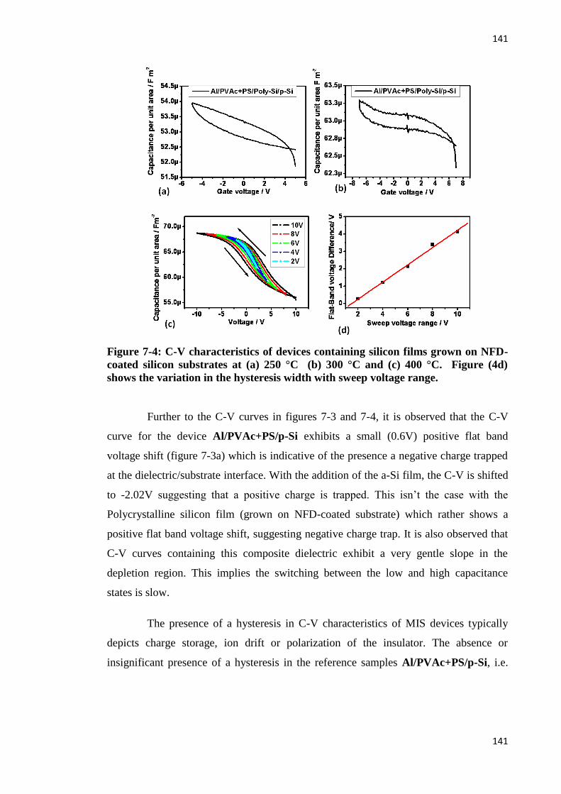
141
141
Figure 7-4: C-V characteristics of devices containing silicon films grown on NFD-
coated silicon substrates at (a) 250 °C (b) 300 °C and (c) 400 °C. Figure (4d)
shows the variation in the hysteresis width with sweep voltage range.
Further to the C-V curves in figures 7-3 and 7-4, it is observed that the C-V
curve for the device Al/PVAc+PS/p-Si exhibits a small (0.6V) positive flat band
voltage shift (figure 7-3a) which is indicative of the presence a negative charge trapped
at the dielectric/substrate interface. With the addition of the a-Si film, the C-V is shifted
to -2.02V suggesting that a positive charge is trapped. This isn’t the case with the
Polycrystalline silicon film (grown on NFD-coated substrate) which rather shows a
positive flat band voltage shift, suggesting negative charge trap. It is also observed that
C-V curves containing this composite dielectric exhibit a very gentle slope in the
depletion region. This implies the switching between the low and high capacitance
states is slow.
The presence of a hysteresis in C-V characteristics of MIS devices typically
depicts charge storage, ion drift or polarization of the insulator. The absence or
insignificant presence of a hysteresis in the reference samples Al/PVAc+PS/p-Si, i.e.
142
142
those containing only the insulator suggests that no charge is stored in them. Similar
observations have been made with different insulators [362-365]. Furthermore, with the
incorporation of a-Si in the devices Al/PVAc+PS/a-Si/p-Si no hysteresis was observed
which further suggests that charge was not stored in the a-Si films except at the
interfaces as indicated by the shift in flat band voltage. The hysteresis in the device
with the Polycrystalline silicon film is thus an indication of charge storage in these
films. The anticlockwise hysteresis suggests that electrons are injected from the p-Si
substrate into the Polycrystalline silicon film when a negative bias is applied on the Al
electrode and ejected when a positive bias is applied on the Al electrode. Films
containing the Polycrystalline silicon films grown on the NFD-coated substrates at 250,
300 and 400 °C all showed charge storage. The amount of charge store in these films
directly relates to the difference in flat-band voltage shift between the forward and
reverse ramps ( FBFBFB VVV ) and can be estimated by
FBVCQ (7-1)
where C is the capacitance at accumulation.
Given that the gate insulator PVAc + PS is organic and known to contain lots
of defects, it was necessary to dispel doubts that these hysteresis obtained with
incorporation of polycrystalline silicon films in the MIS devices were actually due to
charge storage in the polycrystalline silicon films and not due to insulating material
defects. Optimized Si3N4 replaced the organic dielectric in the MIS devices and similar
observations as with the organic were noted. These also revealed insignificant hysteresis
with the reference devices and large hysteresis with those containing the Polycrystalline
silicon films. The graphs are shown in figures 7-5 and 7-6 respectively. The tiny
hysteresis in the reference samples in figure 7-5a can be attributed to charge traps in the
silicon nitride. The C-V curves are shifted to the left, implying that there is a positive
interface charge at the p-Si/nitride interface. This means a higher negative voltage will
need to be applied on the Al top gate to change from inversion to accumulation. The C-
V curves also show a more abrupt change from inversion to accumulation meaning a
higher switching speed than the organic dielectric counterparts. The C-V curves are also

143
143
more shifted to the left of 0V showing that a positive charge is trapped at the interfaces
between the nitride and the p-Si substrate.
-14 -12 -10 -8 -6 -4 -2 0 2 4
0.2
0.4
0.6
0.8
1.0
N
orm
ali
ze
d C
ap
ac
ita
nc
e C
/Cm
ax
Gate Voltage / V
Al / Si3N
4 / p-Si
-15 -10 -5 0 5 10 15
0.4
0.6
0.8
1.0
No
rmalize C
ap
acit
an
ce C
/Cm
ax
Gate voltage / V
Al/Si3N
4/a-Si/Si
3N
4/p-Si
Figure 7-5: Normalized C-V curves of MIS devices with (a) ~50nm silicon nitride
only, (b) silicon nitride and a-Si. The thicknesses (in nm) of films in the device in
(b) were Al/50/100/15/p-Si, for the configuration Al/Si3N4/a-Si/Si3N4/p-Si. The
small hysteresis can be attributed to charge traps in the nitride.
The Polycrystalline silicon-containing devices also exhibited hystereses whose
sizes increased with increase in sweep voltage range as shown in figure 7-6a. As
aforementioned, the hysteresis width directly relates to the amount of charge stored in
the poly-film. Assuming all the charge was stored in the polycrystalline silicon film and
none in the dielectric (because of insignificant hysteresis as observed in figure 7-5a), it
was possible to estimate the different electron densities (number of trapped electrons per
unit area) for the different voltage sweep ranges using the simple relation
19106.1 x
VCn FB (7-2)
c is the capacitance per unit area at accumulation which from figure 7-6a below is 110
nF cm-2
, 1.6 x 10⁻¹⁹
C is the magnitude of electron charge. Table 7-1 shows the
calculated electron density for a MIS device containing silicon film grown on NFD-
coated p-Si substrate. The configuration of the device is Al/Si3N4/Poly-Si/Si3N4/p-Si.
The thickness of the NFD-Polycrystalline silicon film is ~100 nm and the top and
bottom nitride layers are 50 nm and 15 nm respectively. The C-V hysteresis were

144
144
anticlockwise and as mentioned above, this means charge injection from the p-Si
bottom gate.
Table 7-1: The hysteresis width and charge density for various sweep voltage
ranges.
Voltage Sweep range / V ΔVFB = (VFB+ - VFB
-) /volts Electron density / cm-2
±4 0.75 5.16 * 1011
±6 1.6 1.10 * 1012
±8 2.1 1.44 * 1012
±10 3.4 2.34 * 1012
-10 -5 0 5 10
20.0n
40.0n
60.0n
80.0n
100.0n
120.0n
Cap
acit
an
ce d
en
sit
y / F
cm
-2
Gate voltage / V
10V
8V
6V
4V
4 5 6 7 8 9 10
5.0x10¹¹
1.0x10¹²
1.5x10¹²
2.0x10¹²
2.5x10¹²
Ele
ctr
on
den
sit
y / c
m-2
Voltage sweep range
Figure 7-6: C-V curves of MIS devices with (a) silicon nitride + Polycrystalline
silicon at various sweep voltage ranges. 5b shows the charge density variation with
sweep voltage range. The Polycrystalline silicon thickness in the device is ~ 100 nm
and the top and bottom nitride layers are ~50 and 15 nm respectively
The increase in charge density with sweep voltage range shows that more charge is
injected into the floating gate NFD-grown Polycrystalline silicon as electrons acquire
more energy due to the increase in voltage. For the ±10V sweep range, the electron
density as calculated using equation (7-2) was ~ 2.34 x 10¹²
cm-2
. It was also observed
that the switching between the low and high capacitance states was higher for devices
with nitride dielectric than with the organic composite dielectric encountered before.
This is evident from the slopes of the transition regions from inversion to accumulation
in the graphs in figures 7-5 and 7-6a above.
(a) (b)

145
145
7.4 Memory Characteristics
Memory behaviour of 250, 300 and 400 °C Polycrystalline silicon grown films
were investigated through leakage current-voltage (I-V) and capacitance-voltage (C-V)
measurements using the two terminal device containing stacked layers of silicon nitride
gate material and silicon films grown with the aid of seeding material from NFD. The
stack form a memory capacitor with a thin Si3N4 film of ~8-12 nm as a tunnel layer on
an n+-Si substrate, a Polycrystalline silicon film of thickness ~45-50 nm and another
protective Si3N4 insulating layer of 25-30 nm. The device fabrication was completed by
evaporating Al onto the nitride top layer using a shadow mask as describe above. No
further heat-treatment process was performed after this stage.
7.4.1 Leakage Current
-6 -4 -2 0 2 4 6
10p
100p
1n
10n
T=250 oC
Cu
rren
t / A
Gate voltage / V
Al/Si3N
4/a-Si/Si
3N
4/n-Si
Al/Si3N
4/Poly-Si/Si
3N
4/n-Si
-6 -4 -2 0 2 4 6
10p
100p
1n
10n
T = 300 oC
Cu
rren
t / A
Gate voltage / V
Al/Si3N
4/Poly-Si/Si
3N
4/n-Si
Al/Si3N
4/a-Si/Si
3N
4/n-Si
-10 -5 0 5 101p
10p
100p
1n
10n
100n
T = 400 oC
Cu
rre
nt
/ A
Gate voltage / V
Al/Si3N
4/Poly-Si/Si
3N
4/n-Si
Al/Si3N
4/a-Si/Si
3N
4/n-Si
Figure 7-7:I-V curves of devices with silicon films grown on uncoated (broken red
lines) and on NFD-coated substrates (solid black lines) at (a) 250, (b) 300 and (c)
400 °C.
(b) (a)
(c)
146
146
The leakage currents for devices with films grown at different temperatures are
shown in figure 7-7. All 3 graphs indicate that there is a significant increase in current
for devices containing polycrystalline silicon films compared to those a-Si films.
Furthermore, a more regular and consistent hysteresis is obtained with the
Polycrystalline silicon devices compared to the noisy curves of the a-Si devices. The
lower current in a-Si device was expected as the material is more insulating and acts as
a dielectric. A hysteresis in an I-V curve typically signifies charge storage in an
insulator. The absence of a significant hysteresis for the devices even containing a-Si
films was evidence that no significant amount of charge was stored in the a-Si film as
well as in the Si3N4 insulator. The hysteresis observed in the device containing
polycrystalline silicon film can thus be attributed to charge storage in the polycrystalline
silicon film. The clockwise nature of the hysteresis signifies that electrons are injected
into the polycrystalline silicon films from the substrates for positive gate biases by
tunnelling through the thin Si3N4 layer into the film, and extracted for negative gate
biases.
7.4.2 Memory Window
The memory window can be compared with the hysteresis of the C-V curves of
a capacitive device since the presence of a hysteresis signifies charge storage in either
the insulator or active layer of the capacitive device. The devices containing
Polycrystalline silicon films exhibited a very significant hysteresis as voltages were
ramped from positive to negative and back to positive as shown in figure 7-8 below.
Conversely, no significant hysteresis was observed with the a-Si devices. As mentioned
above, the hysteresis obtained with memory devices on n-type Si substrates increased
with ramp voltage limit as similarly observed with the p-type Si substrate devices thus
signifying a larger memory window and thus larger charge stored. It was also observed
that the hysteresis and thus memory window was larger for devices grown at 400 °C
than at 300 °C and that at 250 °C was even less pronounced. This suggests that growth
temperature of the material had a profound effect on the material quality and that the
films were more poly-crystalline at higher temperature. This presence of a hysteresis
confirmed results from leakage current-voltage (I-V) curves obtained prior to
performing the C-V measurements. The hysteresis was also clockwise as similarly
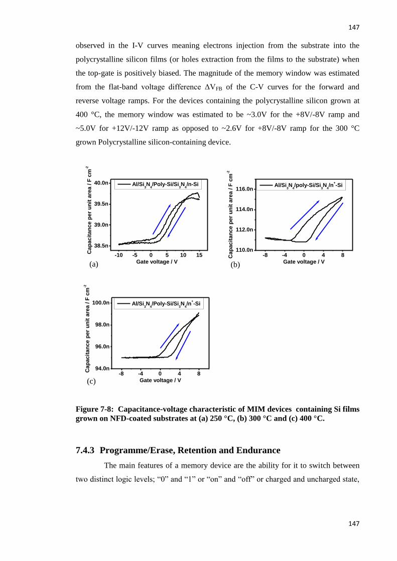
147
147
observed in the I-V curves meaning electrons injection from the substrate into the
polycrystalline silicon films (or holes extraction from the films to the substrate) when
the top-gate is positively biased. The magnitude of the memory window was estimated
from the flat-band voltage difference ΔVFB of the C-V curves for the forward and
reverse voltage ramps. For the devices containing the polycrystalline silicon grown at
400 °C, the memory window was estimated to be ~3.0V for the +8V/-8V ramp and
~5.0V for +12V/-12V ramp as opposed to ~2.6V for +8V/-8V ramp for the 300 °C
grown Polycrystalline silicon-containing device.
-10 -5 0 5 10 15
38.5n
39.0n
39.5n
40.0n
Cap
acit
an
ce p
er
un
it a
rea / F
cm
-2
Gate voltage / V
Al/Si3N
4/Poly-Si/Si
3N
4/n-Si
-8 -4 0 4 8110.0n
112.0n
114.0n
116.0n
Cap
acit
an
ce p
er
un
it a
rea / F
cm
-2
Gate voltage / V
Al/Si3N
4/poly-Si/Si
3N
4/n
+-Si
-8 -4 0 4 894.0n
96.0n
98.0n
100.0n
Cap
acit
an
ce p
er
un
it a
rea / F
cm
-2
Gate voltage / V
Al/Si3N
4/Poly-Si/Si
3N
4/n
+-Si
Figure 7-8: Capacitance-voltage characteristic of MIM devices containing Si films
grown on NFD-coated substrates at (a) 250 °C, (b) 300 °C and (c) 400 °C.
7.4.3 Programme/Erase, Retention and Endurance
The main features of a memory device are the ability for it to switch between
two distinct logic levels; “0” and “1” or “on” and “off” or charged and uncharged state,
(a) (b)
(c)

148
148
and for it to be able to maintain the stored charge either when powered or even when
power is turned off. The memory is said to be non-volatile when it is capable of
maintaining the stored charge for a period of time without being powered.
In order to elucidate the memory programming behaviour of the MIM
capacitive memory device, use was made of different voltage pulses for write, erase and
read. Figure 7-9 shows how the device behaviour followed the applied pulses for the
MIM device containing silicon films grown on NFD-coated substrate. A write pulse of
+8V was applied to the device. This was followed by a read voltage pulse of +1V and
then a -8V erase pulse before another +1V read pulse. It was observed that the
Polycrystalline silicon device could be switched from the low capacitance state (“1”-
state) to high capacitance state (“0”-state) by the application of these voltages. Only 5
cycles of write/erase are shown for clarity. The capacitances at the read voltage of +1V
after each write and erase stayed constant for well over hundreds of complete cycles.
This same pattern of events was also observed for the device containing Polycrystalline
silicon grown at 400 °C. In this case the device was written and erased at ±8V
respectively and read at +2V as shown in figure 7-9b.
0 50 100 150 200 250 300
1.98n
2.00n
2.02n
2.04n
2.06n
0 50 100 150 200 250 300
-8
-4
0
4
8
"1"
"0"
Cap
acit
an
ce / F
Time / S
Pu
lse g
ate
vo
ltag
e / V
0 50 100 150 200 250 300
740.0p
750.0p
760.0p
770.0p
780.0p
-8
-4
0
4
8
R
W
"0"
"1"
Ca
pa
cit
an
ce
/ F
Time / s
EA
pp
lie
d p
uls
e /
V
Figure 7-9: Capacitance-time graphs showing device switching behaviours between
states "on" and "off" or "0" and "1" when different voltage pulses for write, erase
and read are applied, (a) 300 °C device and (b) 400 °C device.
For the device containing polycrystalline silicon grown at 250 °C, the two
levels for “1” and “0” were not clearly distinguishable and so no further studies were
carried out with this device. However, since it behaved identically to the a-Si devices, it
suggests that these films are more inclined to being amorphous than crystalline. This
observation ties with the photoconductivity and optical band gap measurement which
(a) (b)

149
149
showed that the optical band gap was ~1.65-1.8 eV which is in the range of that of a-Si,
and the photosensitivity was in the order of 102 and not 10
0 like for those grown at
higher temperatures.
To assess the long term retention capability of the memory devices, a write
pulse of +8V was applied followed by 100,000 read pulses. An erase pulse of +8V was
subsequently applied which then switched the device from the “on” to the “off” state.
This was closely followed by 100,000 read pulses of +1V for the 300 °C Polycrystalline
silicon grown device (+2V for the 400 °C device). The “on” and “off” states did not
meet at the end of final read process as observed on the graphs in figure 7-10 revealing
an incredible retention capability.
Figure 7-10: Capacitance-time variation at the written (“0”) and erased (“1”) -
state of devices at (a) 300 °C and (b) 400 °C.
The observed capacitance closure in the devices can be associated to the
memory window closure observed in various memory devices [366-369]. This memory
window closure depicts charge lost from the device. Nonetheless, these states stayed
well separated in excess of 2.1x10⁴ s suggesting that charge stored could be retained
well above this time. This demonstrates non-volatility for this device. By fitting suitable
curves to the data, it was realised that the capacitance-time for the “0” state fitted
approximately well to the equation
tACC ln0 (7-3)

150
150
where Co is the intercept on the capacitance axis and A is the gradient of the capacitance
against the ln(t) graph. From equation (7-3),
A
cct 0exp (7-4).
Co and A are obtained from the linear fit of capacitance – ln(t) graph. Assuming that the
capacitance of the “1” state stays fairly constant with time t as observed in the graphs in
figure 7-10, the time for the capacitance of the “0” to decay to the “1” state can be
estimated using equation (7-4). For the device studied in figure 10 above, t has been
estimated to be ~19 days and 21 days respectively for the 300 °C and 400 °C devices
respectively. This represents the retention time of the device. Even though the retention
time is much less than the 10 years required for functional device, it is nonetheless
extraordinary given the very youthful stage of the development of the technique. It thus
presents a remarkable potential for its use in glass compatible flash memory and
particularly 3-D flash memory. This is particularly so given the simplicity of the
technique, the low growth temperatures and the fact that its development is still in the
infancy stage. It is believed that if well harnessed, this technique could be beneficial not
only to the flash memory industries but also to other industries requiring poly-S films
such as the photovoltaic industry.
7.5 Summary
This chapter was aimed at investigating the applicability of silicon structures
grown on NFD-coated substrates in memory devices. Devices with silicon films grown
on NFD-coated substrates have exhibited charge storage In addition to that, these
devices incorporating silicon on NFD-coated substrates exhibit some switching action
between high-capacitance (“0”-state) and low capacitance (“1”-state). This is analogous
to the programmed and erased states of a memory device. Furthermore, the devices are
found to exhibit non-volatility as the capacitance at the erased and programmed states
stay separated well above 6 hours. An estimate of the retention time of 20 days has been
obtained based on some curve fitting the behaviour of the capacitance-time curves. No
heat-treatment was performed these devices after the deposition of the films.

151
151
Chapter 8. Conclusion and Recommendations
for Further Research
8.1 Introduction
The chapter has as objective to summarize the major results of this thesis. The
objectives of this thesis were to develop a novel low temperature technique for growing
polycrystalline silicon films at temperatures ≤ 400°C and to investigate the possibility
of using these films as the FG charge storage medium in flash NVM with the possibility
of extending their use in 3-D flash memory and to study the retention and endurance
behaviour of memory devices with FG material fabricated by the novel technique.
Despite the myriad of problems encountered during the execution of this project, a
number of results have been obtained, which in themselves may set as a spring board to
further studies of this novel low thermal budget technique of growing silicon structures.
Summarized below are the major contributions from this thesis and the
recommendations for further work based on the observed results.
8.2 Major Results
As observed in the early chapters of this thesis, Ni particles have been used for
various purposes and for the growth of Polycrystalline silicon films using the MILC and
MIC processes. This has often been done either by growing the a-Si films directly on
deposited Ni particles on substrates or by depositing Ni film on a-Si films accompanied
by annealing. This research has for the first time demonstrated the possibility of
growing polycrystalline silicon structures directly on substrates coated with the Ni
source material, nickel formate dihydrate that decomposes in-situ the PECVD process
to provide a seeding for the nucleation and growth of Polycrystalline silicon films.
Furthermore, the films grown on these NFD-coated substrates have been found to have
the capability of charge storage. In a 2-terminal memory device, these films have clearly
shown non-volatile memory behaviour. Thus in the course of developing this growth
technique, the following were major contributions:
1. More uniform and thicker films of NFD on glass and silicon substrates
resulted from dip-coating. Various factors were found to affect the

152
152
thickness of the films, particularly concentration of solution, the choice of
the solvent, the immersion time and the withdrawal speed. Water was
found to be the best solvent and the best optimized conditions for NFD
coatings were obtained.
2. Through FTIR, UV-VIS, AFM and conductivity measurements, it has been
shown that films grown under identical RF PECVD reactor conditions on
uncoated substrates and NFD-coated substrates show distinct
characteristics. While those on uncoated substrates exhibit amorphous
properties, those grown on NFD coated substrates without further annealing
exhibit polycrystalline properties. For instance, under the same condition,
an optical band gap of 1.22 eV was obtained for NFD-coated substrate
films and 1.78 eV for uncoated substrate films.
3. Through electrical measurements on MIS and MIM devices, silicon films
grown on NFD-coated substrates at ≤ 400 °C and ≥ 250 °C have been
found to exhibit electron storage in the order of 1012
cm-2
. Those grown at
300 and 400 °C have exhibited non-volatile memory characteristics even
though with an initial estimated retention time of only ~20 days.
In the entire work, all major process conditions were less ≤ 400 °C. Thus the
major contribution is the demonstration of a new low thermal budget growth method of
Polycrystalline silicon. This method has the potentials of growing quality silicon
structures capable of being applied in memory device fabrication. The method is glass
compatible since process temperatures are within the allowable limits of glass. The
exhibition of non-volatile memory behaviour of the films grown by this new technique
could open up a window for their application in systems-on-glass industry especially
where memory integration is required. Furthermore, concerning 3-D flash memory, the
techniques meets the process temperature requirements of ≤ 400 °C thus speeding the
way to higher storage capacity, higher speeds, and better endurance for future 3-D flash
memory than today’s conventional planar memories.
153
153
8.3 Recommendation for Further Studies
This research has demonstrated a new low temperature method of growing
polycrystalline silicon and has also demonstrated their possible use in memory devices.
Despite some of the encouraging results, there are still many unanswered questions
about this low temperature growth method that need to be addressed. This thus opens up
different ways through which this research can be expanded in order to address some of
the unanswered issues. This section thus deals with some recommended areas of further
research to address some cited issues.
8.3.1 Dip-coating of NFD
During the investigation of the dip-coating of NFD, it was found that the
concentration of NFD and other factors affect the final thickness of the films. It was
proposed that the diffusion-adsorption mechanism was mostly responsible for the
increase in thickness of the films with increase in immersion time. However, only single
dip-coating cycles (i.e., the process of lowering the substrate into the solution, keeping
it in the solution for an immersion time and withdrawing from the solution is one cycle)
of substrates were investigated. It was assumed (after a few trial multiple dipping
cycles) that a second dip of the coated substrate in NFD solution would lead to the film
on the substrate being absorbed into the solution since a concentration gradient will
exist between the films on the substrate and the NFD solution. This however needs to be
explicitly established. This could be done by studying how the films thickness develops
through multiple cycle coatings in different solution concentrations of NFD.
Furthermore, film morphology (uniformity) for different coating conditions should be
established throughout.
8.3.2 Contamination of Si Films
The presence or absence of metallic Ni contaminants in the grown
polycrystalline silicon films was not clearly established. It is important that this should
be established clearly through methods like Secondary ion mass spectrometry (SIMS)
and any other suitable method like total-reflection X-ray fluorescence, inductively
coupled plasma optical emission spectroscopy, RF glow discharge optical emission
spectroscopy, and laser ablation inductively coupled plasma mass spectrometry, so as to

154
154
understand how these metallic contaminants affect the physical and electrical properties
of the films as well as their effects, if any, on the memory device reliability.
Furthermore, the optical band gap was a major factor in the optimization of the films
and to conclude that films on coated substrates were polycrystalline. It is suggested that
other established methods like XRD and Raman spectroscopy should be used to
corroborate the results obtained from UV-Vis spectroscopy and Tauc plots.
8.3.3 Memory
Memory devices exhibited some switching behaviour and some retention of
electrons. However, it was observed that a high percentage of the charge was lost within
the first few minutes. Furthermore, the retention time was far too small compared to
current technology. The cause of these issues and the factors that influence the
reliability of the memory devices should be studied. This could be done by studying the
films for any contaminants as well as investigating different control and tunnel
dielectrics and the interface properties of the device layers.
155
155
References
[1] G. Groeseneken, H. E. Maes, J. V. Hout, and J. S. Witters, "Basics of
Nonvolatile Semiconductor Memory Devices," in Nonvolatile Semiconductor
Memory Technology: A Comprehensive Guide to Understanding and Using
NVSM Devices, W. D. Brown and J. Brewer, Eds.: IEEE Press Series on
Microelectronic Systems, October 15, 1997.
[2] M. Yang, "Flash memory market shares," in isuppli, 2010.
[3] L. Mearian, "High prices are forcing solid state storage vendors to look for
alternatives," in Is NAND flash memory a dying technology?: TECHWORLD,
2010.
[4] K. Kim, "Future memory technology: Challenges and opportunities," in
International Symposium on VLSI Technology, Systems, and Applications,
Proceedings, Hsinchu, 2008, pp. 5-9.
[5] G. E. Moore, "Cramming more components onto integrated circuits," Electronics, vol.
38, pp. 114-117, 1965.
[6] J. Kim, A. J. Hong, S. M. Kim, E. B. Song, J. H. Park, J. Han, S. Choi, D. Jang,
J. T. Moon, and K. L. Wang, "Novel Vertical-Stacked-Array-Transistor (VSAT)
for ultra-high-density and cost-effective NAND Flash memory devices and SSD
(Solid State Drive)," Symposium on VLSI Technology, Digest of Technical
Papers, pp. 186-187, 2009.
[7] R. Bez, E. Camerlenghi, A. Modelli, and A. Visconti, "Introduction to flash
memory," Proceedings of the IEEE, vol. 91, pp. 489-502, 2003.
[8] ITRS, "ITRS 2009 Edition," 2010.
[9] C. Y. Lu, K. Y. Hsieh, and R. Liu, "Future challenges of flash memory
technologies," Microelectronic Engineering, vol. 86, pp. 283-286, 2009.
[10] J. Kim, A. J. Hong, M. K. Sung, E. B. Song, H. P. Jeung, J. Han, S. Choi, D.
Jang, J. T. Moon, and K. L. Wang, "Novel vertical-stacked-array-transistor
(VSAT) for ultra-high-density and cost-effective NAND flash memory devices
and SSD (solid state drive)," in Digest of Technical Papers - Symposium on
VLSI Technology, 2009, pp. 186-187.
[11] G. Molas, D. Deleruyelle, B. De Salvo, G. Ghibaudo, M. Gely, S. Jacob, D.
Lafond, and S. Deleonibus, "Impact of few electron phenomena on floating-gate
memory reliability," in Technical Digest - International Electron Devices
Meeting, IEDM, 2004, pp. 877-880.
[12] G. Atwood, "Future directions and challenges for ETox Flash memory scaling,"
IEEE Transactions on Device and Materials Reliability, vol. 4, pp. 301-305,
2004.
[13] G. Atwood, "The evolution of phase-change memory," in EE Times
http://www.eetimes.com/design/memory-design/4204936/The-evolution-of-
phase-change-memory, 26 July 2010.
[14] S. Tiwari, F. Rana, H. Hanafi, A. Hartstein, E. F. Crabbé, and K. Chan, "A
silicon nanocrystals based memory," Applied Physics Letters, p. 1377, 1995.
[15] S. Kolliopoulou, D. Tsoukalas, P. Dimitrakis, P. Normand, S. Paul, C. Pearson,
A. Molloy, and M. C. Petty, "Field effect devices with metal nanoparticles
integrated by Langmuir-Blodgett technique for non-volatile memory
applications," Journal of Physics: Conference Series, vol. 10, pp. 57-60, 2005.
156
156
[16] J. De Blauwe, "Nanocrystal nonvolatile memory devices," IEEE Transactions
on Nanotechnology, vol. 1, pp. 72-77, 2002.
[17] K. Kim and S. Y. Lee, "Memory technology in the future," Microelectronic
Engineering, vol. 84, pp. 1976-1981, 2007.
[18] D. Ha and K. Kim, "Recent advances in high density phase change memory
(PRAM)," in International Symposium on VLSI Technology, Systems, and
Applications, Proceedings, Hsinchu, 2007.
[19] K. Kim and G. Jeong, "Memory technologies in the nano-era: Challenges and
opportunities," in Digest of Technical Papers - IEEE International Solid-State
Circuits Conference, San Francisco, CA, 2005.
[20] R. Bailey, G. Fox, J. Eliason, M. Depner, D. Kim, E. Jabillo, J. Groat, J.
Walbert, T. Moise, S. Summerfelt, K. R. Udayakumar, J. Rodriquez, K.
Remack, K. Boku, and J. Gertas, "FRAM memory technology - Advantages for
low power, fast write, high endurance applications," in Proceedings - IEEE
International Conference on Computer Design: VLSI in Computers and
Processors, San Jose, CA, 2005, p. 485.
[21] K. Kim, J. H. Choi, J. Choi, and H. S. Jeong, "The future prospect of nonvolatile
memory," in 2005 IEEE VLSI-TSA - International Symposium on VLSI
Technology - VLSI-TSA-TECH, Proceedings of Technical Papers, Hsinchu,
2005, pp. 88-94.
[22] K. Kinam, J. Gitae, J. Hongsik, and L. Sungyung, "Emerging memory
technologies," in Proceedings of the Custom Integrated Circuits Conference,
San Jose, CA, 2005, pp. 416-419.
[23] H. Li and Y. Chen, "Emerging non-volatile memory technologies: From
materials, to device, circuit, and architecture," in Midwest Symposium on
Circuits and Systems, Seattle, WA, pp. 1-4.
[24] S. Natarajan and A. Alvandpour, "Emerging memory technologies - Mainstream
or hearsay?," in 2005 IEEE VLSI-TSA International Symposium on VLSI Design,
Automation and Test,(VLSI-TSA-DAT), Hsinchu, 2005, pp. 222-228.
[25] J. A. Hutchby, G. I. Bourianoff, V. V. Zhirnov, and J. E. Brewer, "Emerging
research memory and logic technologies," IEEE Circuits and Devices Magazine,
vol. 21, pp. 47-51, 2005.
[26] D. Ielmini, D. Mantegazza, A. L. Lacaita, A. Pirovano, and F. Pellizzer,
"Switching and programming dynamics in phase-change memory cells," Solid-
State Electronics, vol. 49, pp. 1826-1832, 2005.
[27] N. Derhacobian, S. C. Hollmer, N. Gilbert, and M. N. Kozicki, "Power and
Energy Perspectives of Nonvolatile Memory Technologies," Proceedings of the
IEEE, vol. 98, pp. 283-298.
[28] W. Xiaoxia, L. Jian, Z. Lixin, E. Speight, and X. Yuan, "Power and performance
of read-write aware Hybrid Caches with non-volatile memories," in Design,
Automation & Test in Europe Conference & Exhibition, 2009. DATE '09., 2009,
pp. 737-742.
[29] D. Prime and S. Paul, "Overview of organic memory devices," Philosophical
Transactions of the Royal Society A: Mathematical, Physical and Engineering
Sciences, vol. 367, pp. 4141-4157, 2009.
[30] J. Ouyang, C. W. Chu, R. J. H. Tseng, A. Prakash, and Y. Yang, "Organic
Memory Device Fabricated Through Solution Processing," in Proceedings of the
IEEE, 2005, pp. 1287-1296.

157
157
[31] T. Furukawa, "Structure and functional properties of ferroelectric polymer,"
Adv. Colloid Interface Sci., vol. 71-72, pp. 183--208, 1997.
[32] E. C.-S. Yang, C.-J. Liu, T.-S. Chao, M.-C. Liaw, and C. C.-H. Hsu, "Novel di-
directional tunneling NOR (BiNOR) type 3-D flash memory cell," in Digest of
Technical Papers - Symposium on VLSI Technology, 1999, pp. 85-86.
[33] A. H. F. Chou, E. C. S. Yang, C. J. Liu, H. H. Pong, M. C. Liaw, T. S. Chao, Y.
C. King, H. L. Hwang, and C. C. H. Hsu, "Comprehensive study on a novel
bidirectional tunneling program/erase NOR-type (BiNOR) 3-D flash memory
cell," IEEE Transactions on Electron Devices, vol. 48, pp. 1386-1393, 2001.
[34] A. J. Walker, "Sub-50-nm dual-gate thin-film transistors for monolithic 3-D
flash," IEEE Transactions on Electron Devices, vol. 56, pp. 2703-2710, 2009.
[35] S. Koliopoulou, P. Dimitrakis, D. Goustouridis, P. Normand, C. Pearson, M. C.
Petty, H. Radamson, and D. Tsoukalas, "Metal nano-floating gate memory
devices fabricated at low temperature," Microelectronic Engineering, vol. 83,
pp. 1563-1566, 2006.
[36] S. R. Park, K. Y. Kim, C. Choi, K. J. Song, J. H. Park, K. Jeon, S. Lee, T. Y.
Kim, J. E. Lee, S. Lee, S. Park, J. Jang, D. M. Kim, and D. H. Kim,
"Comparative Study on Program/Erase Efficiency and Retention Properties of 3-
D SONOS Flash Memory Cell Array Transistors: Structural Approach from
Double-Gate FET and FinFET to Gate-All-Around FET," Journal of the Korean
Physical Society, vol. 54, pp. 1854-1861, May 2009.
[37] D. Park, K. Kim, and B. I. Ryu, "3-dimensional nano-CMOS transistors to
overcome scaling limits," in International Conference on Solid-State and
Integrated Circuits Technology Proceedings, ICSICT, 2004, pp. 35-40.
[38] R. Tsuchiya, M. Izawa, and S. Kimura, "Prospects for Si Semiconductor Devices
and Manufacturing Technologies in Nanometer Era," Hitachi Review, vol. 52,
pp. 46-55, June 2006 2006.
[39] H. Tanaka, M. Kido, K. Yahashi, M. Oomura, R. Katsumata, M. Kito, Y.
Fukuzumi, M. Sato, Y. Nagata, Y. Matsuoka, Y. Iwata, H. Aochi, and A.
Nitayama, "Bit cost scalable technology with punch and plug process for ultra
high density flash memory," Symposium on VLSI Technology, Digest of
Technical Papers, pp. 14-15, 2007.
[40] S. M. Jung, J. Jang, W. Cho, H. Cho, J. Jeong, Y. Chang, J. Kim, Y. Rah, Y.
Son, J. Park, M. S. Song, K. H. Kim, J. S. Lim, and K. Kim, "Three
dimensionally stacked NAND flash memory technology using stacking single
crystal Si layers on ILD and TANOS structure for beyond 30nm node," in
Technical Digest - International Electron Devices Meeting, IEDM, 2006.
[41] E. K. Lai, H. T. Lue, Y. H. Hsiao, J. Y. Hsieh, C. P. Lu, S. Y. Wang, L. W.
Yang, T. Yang, K. C. Chen, J. Gong, K. Y. Hsieh, R. Liu, and C. Y. Lu, "A
multi-layer stackable thin-film transistor (TFT) NAND-type Flash memory," in
Technical Digest - International Electron Devices Meeting, IEDM, 2006.
[42] S. Chen and B. J. Hull, "Method for forming a nanocrystal floating gate for a
flash memory device," in USPTO, H01L 21/02; H01L 21/336 ed. vol.
US2006/0046383 A1 US: Chen, Shenlin and Hull, B. Jeffrey, 2006.
[43] W.-E. Hong, S.-J. Oh, and J.-S. Ro, "Solid phase crystallization of amorphous
silicon at temperatures higher than 600C," Takamatsu, Japan, 2005, pp. 1187-
1190.

158
158
[44] D. L. Young, P. Stradins, E. Iwaniczko, B. To, B. Reedy, Y. Yan, H. M. Branz,
J. Lohr, M. Alvarez, J. Booske, A. Marconnet, and Q. Wang, "Solid phase
crystallization of hot-wire CVD amorphous silicon films," San Francisco, CA,
United states, 2005, pp. 233-238.
[45] L. Haji, P. Joubert, J. Stoemenos, and N. A. Economou, "Mode of growth and
microstructure of polycrystalline silicon obtained by solid-phase crystallization
of an amorphous silicon film," Journal of Applied Physics, vol. 75, pp. 3944-52,
1994.
[46] H. Azuma, A. Takeuchi, T. Ito, H. Fukushima, T. Motohiro, and M. Yamaguchi,
"Pulsed KrF excimer laser annealing of silicon solar cell," Solar Energy
Materials and Solar Cells, vol. 74, pp. 289-94, 2002.
[47] J. Huang, R. Hong, X. Chen, and Z. Wu, "Crystallization of amorphous
hydrogenated SiC films by KrF excimer laser annealing," Guangxue
Xuebao/Acta Optica Sinica, vol. 28, pp. 378-382, 2008.
[48] Y. Ru-Yuan, W. Min-Hang, L. Chihng-Tsung, S. Yan-Kuin, and S. Shyi-Long,
"Low temperature metal induced crystallization of amorphous silicon by nano-
gold-particles," Japanese Journal of Applied Physics, Part 2 (Letters), vol. 45,
pp. 1146-8, 2006.
[49] Y. Soo Young, K. Ki Hyung, K. Chae Ok, O. Jae Young, and J. Jin, "Low
temperature metal induced crystallization of amorphous silicon using a Ni
solution," Journal of Applied Physics, vol. 82, pp. 5865-7, 1997.
[50] S. Y. Yoon, S. J. Park, K. H. Kim, and J. Jang, "Metal-induced crystallization of
amorphous silicon," Thin Solid Films, vol. 383, pp. 34-38, 2001.
[51] J. H. Choi, D. Y. Kim, B. K. Choo, W. S. Sohn, and J. Jang, "Metal induced
lateral crystallization of amorphous silicon through a silicon nitride cap layer,"
Electrochemical and Solid-State Letters, vol. 6, pp. 16-18, 2003.
[52] K. H. Lee, Y. K. Fang, and S. H. Fan, "Au metal-induced lateral crystallization
(MILC) of hydrogenated amorphous silicon thin film with very low annealing
temperature and fast MILC rate," Electronics Letters, vol. 35, pp. 1108-1109,
1999.
[53] R. A. Street, Hydrogenated amorphous silicon. Cambridge ; New York:
Cambridge University Press, 1991.
[54] M. K. Hatalis and D. W. Greve, "Large grain polycrystalline silicon by low-
temperature annealing of low-pressure chemical vapor deposited amorphous
silicon films," Journal of Applied Physics, vol. 63, pp. 2260-2266, 1988.
[55] N. T. Tran, M. P. Keyes, S. Shiffman, G. Liu, and S. J. Fonash, "Comparison of
different processes in the fabrication of crystallized amorphous silicon thin film
transistors," in Conference on Solid State Devices and Materials, Yokohama,
Jpn, 1991, pp. 617-619.
[56] G. A. Bhat, H. S. Kwok, and M. Wong, "Behavior of the drain leakage current in
metal-induced laterally crystallized thin film transistors," Solid-State
Electronics, vol. 44, pp. 1321-1324, 2000.
[57] G. A. Bhat, Z. Jin, H. S. Kwok, and M. Wong, "The effects of MIC/MILC
interface on the performance of MILC-TFTs," in Device Research Conference
Digest, 1998. 56th Annual, 1998, pp. 110-111.
[58] N.-K. Song, Y.-S. Kim, M.-S. Kim, S.-H. Han, and S.-K. Joo, "A Fabrication
Method for Reduction of Silicide Contamination in Polycrystalline-Silicon Thin-

159
159
Film Transistors," Electrochemical and Solid-State Letters, vol. 10, pp. H142-
H144, 2007.
[59] T. H. Ihn, B. I. Lee, T. K. Kim, K. H. Kim, J. W. Shin, P. S. Ahn, W. C. Jeong,
and S. K. Joo, "Fabrication of metal-gate poly-Si TFT's by metal induced lateral
crystallization," in SID International Symposium Digest of Technical Papers,
1997, p. 188.
[60] D. Murley, N. Young, M. Trainor, and D. McCulloch, "An investigation of laser
annealed and metal-induced crystallized polycrystalline silicon thin-film
transistors," Electron Devices, IEEE Transactions on, vol. 48, pp. 1145-1151,
2001.
[61] IBM, "History of IBM Research 1945 - 1998,"
http://www.research.ibm.com/about/past_history.shtml.
[62] Surachit, "Diagram of a computer hard disk drive," in
http://en.wikipedia.org/wiki/File:Hard_drive-en.svg, 24 July 2007.
[63] "SSD Market History - Charting the 30 Year Rise of the Solid State Disk
Market." vol. 2010: http://www.storagesearch.com/chartingtheriseofssds.html.
[64] A. Higginbotham, "SSD vs HDD $/GB in Retail," in Flash Memory Summit
Santa Clara, CA. USA, 2010.
[65] STEC, "Solid State Drive - The Performance and Power Advantages,"
http://www.stec-
inc.com/downloads/whitepapers/Performance_Power_Advantages.pdf.
[66] http://en.wikipedia.org/wiki/File:SRAM_Cell_%286_Transistors%29.svg,
Accessed on 27 October 2010.
[67] "Flash Memory Guide - Portable Flash memory for computers, digital cameras,
cell phones and other devices," http://www.kingston.com/flash_memory_guide/.
[68] D. Kahng and S. M. Sze, "A floating-gate and its application to memory
devices," The Bell System Technical Journal, vol. 46, pp. 1288–1295, 1967.
[69] H. A. R. Wegener, A. J. Lincoln, H. C. Pao, M. R. O'Connell, and R. E.
Oleksiak, "The variable threshold transistor, a new electrically-alterable, non-
destructive read-only storage device," IEEE IEDM Technical Digest, 1967.
[70] D. Frohman-Bentchkowsky, "Memory behavior in a floating-gate avalanche-
injection MOS (FAMOS) structure," Applied Physics Letters, vol. 18, pp. 332-
334, 1971.
[71] D. Frohman-Bentchkowsky, "Famos-A new semiconductor charge storage
device," Solid State Electronics, vol. 17, 1974.
[72] D. Frohman-Bentchkowsky, "A fully decoded 2048-bit electrically
programmable FAMOS read-only memory " IEEE Journal of Solid-State
Circuits vol. 6, pp. 301 - 306, 1971.
[73] H. Iizuka, T. Sato, F. Masuoka, K. Ohuchi, H. Hara, H. Tango, M. Ishikawa, and
Y. Takeishi, "Stacked gate avalanche injection type MOS (SAMOS) memory,"
Proceedings of the 4th Conference on Solid-State Devices, Tokyo 1972,
Supplement to the Journal of Japan Society of Applied Physics, vol. 42, pp. 158-
166, 1973.
[74] H. Iizuka, F. Masuoka, S. Tai, and M. Ishikawa, "Electrically alterable
avalanche-injection-type MOS READ-ONLY memory with stacked-gate
structure," Electron Devices, IEEE Transactions on, vol. 23, pp. 379-387, 1976.
160
160
[75] F. Masuoka, M. Asano, H. Iwahashi, T. Komuro, and S. Tanaka, "NEW FLASH
E**2 PROM CELL USING TRIPLE POLYSILICON TECHNOLOGY," in
Technical Digest - International Electron Devices Meeting, 1984, pp. 464-467.
[76] G. Verma and N. Mielke, "Reliability performance of ETOX based flash
memories," in Reliability Physics Symposium 1988. 26th Annual Proceedings.,
International, 1988, pp. 158-166.
[77] S.-W. Lee, B. Moon, C. Park, J.-M. Kim, and S.-W. Kim, "A Case for Flash
Memory SSD in Enterprise Database Applications," in Proceedings of the ACM
SIGMOD, 2008, pp. 1075–1086.
[78] T. Hagiwara, Y. Yatsuda, R. Kondo, S. Minami, T. Aoto, and Y. Itoh, "A 16 kbit
electrically erasable PROM using n-channel Si-gate MNOS technology," Solid-
State Circuits, IEEE Journal of, vol. 15, pp. 346-353, 1980.
[79] Y. Yatsuda, T. Hagiwara, S.-i. Minami, R. Kondo, K. Uchida, and K. Uchiumi,
"Scaling Down MNOS Nonvolatile Memory Devices," Japan Journal of
Applied Physics, vol. 21, pp. 85-90, 1982.
[80] K. I. Lundstrom and C. M. Svensson, "Properties of MNOS structures," IEEE
Transaction of Electronic Devices, vol. ED-19, 1972.
[81] T. Hagiwara, Y. Yatsuda, S. Minami, S. Naketani, K. Uchida, and T. Yasui, "A
5V only 64k MNOS EEPROM," in 6th Non-Volatile Semiconductor Memory
Conference Vail, Colorado, 1983.
[82] P. C. Chen, "Threshold-alterable Si-gate MOS devices," IEEE Transactions of
Electron Devices, vol. 24, p. 584, 1977.
[83] M. C. Chen, H. Y. Yu, N. Singh, Y. Sun, N. S. Shen, X. H. Yuan, G. Q. Lo, and
D. L. Kwong, "Vertical-Si-Nanowire SONOS Memory for Ultrahigh-Density
Application," IEEE Electron Device Letters, vol. 30, pp. 879-881, Aug 2009.
[84] I. H. Cho, B. G. Park, J. D. Lee, T. S. Park, S. Y. Choi, and J. H. Lee, "Body-
Tied Double-Gate SONOS Flash (Omega Flash) Memory Device Built on a
Bulk Si Wafer," Journal of the Korean Physical Society, vol. 44, pp. 83-86,
2004.
[85] B. De Salvo, C. Gerardi, R. Van Schaijk, S. A. Lombardo, D. Corso, C.
Plantamura, S. Serafino, G. Ammendola, M. Van Duuren, P. Goarin, W. Y. Mei,
K. D. Van Jeugd, T. Baron, M. Gély, P. Mur, and S. Deleonibus, "Performance
and reliability Features of advanced nonvolatile memories based on discrete
traps (silicon nanocrystals, SONOS)," IEEE Transactions on Device and
Materials Reliability, vol. 4, pp. 377-387, 2004.
[86] Y. Kim, I. H. Park, S. Cho, J. G. Yun, J. H. Lee, D. H. Kim, G. S. Lee, S. H.
Park, D. H. Lee, W. B. Sim, W. Kim, H. Shin, J. D. Lee, and B. G. Park, "A
Vertical 4-Bit SONOS Flash Memory and a Unique 3-D Vertical NOR Array
Structure," IEEE Transactions on Nanotechnology, vol. 9, pp. 70-77, Jan 2010.
[87] Y. K. Lee, J. S. Sim, S. K. Sung, C. J. Lee, T. H. Kim, J. D. Lee, B. G. Park, D.
H. Lee, and Y. W. Kim, "Multilevel vertical-channel SONOS nonvolatile
memory on SOI," IEEE Electron Device Letters, vol. 23, pp. 664-666, 2002.
[88] S. K. Sung, T. Y. Kim, E. S. Cho, H. J. Cho, B. Y. Choi, C. W. Oh, B. K. Cho,
C. H. Lee, and D. Park, "Fully integrated SONOS flash memory cell array with
BT (body tied)-finFET structure," IEEE Transactions on Nanotechnology, vol.
5, pp. 174-178, 2006.
[89] S. T. Wang, "On the I-V Characteristics of Floating Gate MOS Transistors,"
IEEE Transactions on Electron Devices, vol. 26, pp. 1292-1294, 1979.

161
161
[90] P. Pavan, R. Bez, P. Olivo, and E. Zanoni, "Flash memory cells-an overview,"
Proceedings of the IEEE, vol. 85, pp. 1248-1271, 1997.
[91] P. Heremans, R. Bellens, G. Groeseneken, and H. E. Maes, "Consistent model
for the hot-carrier degradation in N-channel and P-channel MOSFET's," IEEE
Transactions on Electron Devices, vol. 35, pp. 2194-2208, 1988.
[92] C. Hu, S. C. Tam, F.-C. Hsu, P.-K. Ko, T.-Y. Chan, and K. W. Terrill, "HOT-
ELECTRON-INDUCED MOSFET DEGRADATION - MODEL, MONITOR,
AND IMPROVEMENT," IEEE Journal of Solid-State Circuits, vol. SC-20, pp.
295-305, 1985.
[93] S. Tam, P.-K. Ko, and C. Hu, "LUCKY-ELECTRON MODEL OF CHANNEL
HOT-ELECTRON INJECTION IN MOSFET's," IEEE Transactions on
Electron Devices, vol. ED-31, pp. 1116-1125, 1984.
[94] K. Sonoda, M. Tanizawa, S. Shimizu, Y. Araki, S. Kawai, T. Ogura, S.
Kobayashi, K. Ishikawa, T. Eimori, Y. Inoue, Y. Ohji, and N. Kotani, "Compact
modeling of a Flash memory cell including substrate-bias-dependent hot-
electron gate current," IEEE Transactions on Electron Devices, vol. 51, pp.
1726-1730, 2004.
[95] P. E. Cottrell, R. R. Troutman, and T. H. Ning, "HOT-ELECTRON EMISSION
IN N-CHANNEL IGFET's," IEEE Trans Electron Devices, vol. ED-26, pp. 520-
533, 1979.
[96] T. H. Ning, C. M. Osburn, and H. N. Yu, "Emission probability of hot electrons
from silicon into silicon dioxide," Journal of Applied Physics, vol. 48, pp. 286-
293, 1977.
[97] M. Lenzlinger and E. H. Snow, "Fowler-nordheim tunneling into thermally
grown SiO2," Journal of Applied Physics, vol. 40, pp. 278-283, 1969.
[98] B. V. Zeghbroeck, Principles of Semiconductors Devices, 2007.
[99] N. M. Ravindra and J. Zhao, "Fowler-Nordheim tunneling in thin SiO2 films "
Modelling and Simulation in Materials Science and Engineering, vol. 1, pp.
197-201, 1992.
[100] G. Verma and N. Mielke, "RELIABILITY PERFORMANCE OF ETOX
BASED FLASH MEMORIES," in Annual Proceedings - Reliability Physics
(Symposium), 1988, pp. 158-166.
[101] R. Verma, "Flash memory quality and reliability issues," in Memory
Technology, Design and Testing, 1996. Records of the 1996 IEEE International
Workshop on, 1996, pp. 32-36.
[102] P. Muroke, "Flash Memory Field Failure Mechanisms," in IEEE 44th Annual
International Reliability Physics Sypmposium San Jose, 2006, pp. 313-316.
[103] A. Modelli and B. Ricco, "Electric field and current dependence of SiO2
intrinsic breakdown," IEEE IEDM Technical Digest, pp. 148-151, 1984.
[104] D. J. DiMaria and D. R. Kerr, "Interface effects and high conductivity in oxides
grown from polycrystalline silicon," Applied Physics Letters, vol. 27, pp. 505-
507, 1975.
[105] L. Faraone, R. D. Vibronek, and J. T. McGinn, "Characterization of thermally
oxidized n<sup>+</sup>polycrystalline silicon," Electron Devices, IEEE
Transactions on, vol. 32, pp. 577-583, 1985.
[106] L. Faraone, "Thermal SiO2 films on n+ polycrystalline silicon: Electrical
conduction and breakdown," Electron Devices, IEEE Transactions on, vol. 33,
pp. 1785-1794, 1986.

162
162
[107] M. Aminzadeh, S. Nozaki, and R. V. Giridhar, "Conduction and charge trapping
in polysilicon-silicon nitride-oxide-silicon structures under positive gate bias,"
Electron Devices, IEEE Transactions on, vol. 35, pp. 459-467, 1988.
[108] J. D. Lee, J. H. Choi, D. Park, and K. Kim, "Degradation of tunnel oxide by FN
current stress and its effects on data retention characteristics of 90-nm NAND
flash memory cells," in Annual Proceedings - Reliability Physics (Symposium),
2003, pp. 497-501.
[109] M. Park, A. Eungjin, C. Eunsuk, K. Keonsoo, and L. Won-Seong, "The Effect of
Negative VTH of NAND Flash Memory Cells on Data Retention
Characteristics," Electron Device Letters, IEEE, vol. 30, pp. 155-157, 2009.
[110] Y. Hong, K. Hyunjae, P. Sung-il, K. Jongseob, L. Sung-Hoon, C. Jung-Ki, H.
Duhyun, K. Chulsung, P. Mincheol, L. Keun-Ho, P. Young-Kwan, S. Jai
Kwang, and K. Jeong-Taek, "Reliability Issues and Models of sub-90nm NAND
Flash Memory Cells," in Solid-State and Integrated Circuit Technology, 2006.
ICSICT '06. 8th International Conference on, 2006, pp. 760-762.
[111] "Portable Flash memory for computers, digital cameras, cell phones and other
devices," in Flash Memory Guide: Kingston Technology Corporation. 17600
Newhope Street, Fountain Valley, CA 92708 USA,
http://www.kingston.com/products/pdf_files/FlashMemGuide.pdf.
[112] H. P. Belgal, N. Righos, I. Kalastirsky, J. J. Peterson, R. Shiner, and N. Mielke,
"A new reliability model for post-cycling charge retention of flash memories," in
Reliability Physics Symposium Proceedings, 2002. 40th Annual, 2002, pp. 7-20.
[113] D. Ielmini, A. S. Spinelli, A. L. Lacaita, L. Confalonieri, and A. Visconti, "New
technique for fast characterization of SILC distribution in flash arrays," in
Annual Proceedings - Reliability Physics (Symposium), 2001, pp. 73-80.
[114] D. Ielmini, A. S. Spinelli, A. L. Lacaita, R. Leone, and A. Visconti,
"Localization of SILC in Flash memories after program/erase cycling," in
Annual Proceedings - Reliability Physics (Symposium), 2002, pp. 1-6.
[115] D. Ielmini, A. S. Spinelli, A. L. Lacaita, and A. Modelli, "Statistical modeling of
reliability and scaling projections for flash memories," in Technical Digest -
International Electron Devices Meeting, 2001, pp. 703-706.
[116] G. Iannaccone, "Evaluation of program, erase and retention times of flash
memories with very thin gate dielectric," in Nanotechnology, 2002. IEEE-NANO
2002. Proceedings of the 2002 2nd IEEE Conference on, 2002, pp. 247-250.
[117] J. J. Makwana and D. K. Schroder, "A Nonvolatile Memory Overview ":
http://aplawrence.com/Makwana/nonvolmem.html, 2004.
[118] D. Aadsen, L. Fenstermaker, F. Higgins, K. Ilyoung, J. Lewandowski, and J. J.
Nagy, "Test algorithm for memory cell disturb failures," in Memory Technology,
Design and Testing, 1998. Proceedings. International Workshop on, 1998, pp.
53-56.
[119] S. K. Lai, "Flash memories: Successes and challenges," Ibm Journal of Research
and Development, vol. 52, pp. 529-535, 2008.
[120] D. Wilson, "Flash memory prices dropping, but SSDs may be too far behind," in
Solid state drives held back by high NAND prices: TechEYE
http://www.techeye.net/chips/solid-state-drives-held-back-by-high-nand-prices,
2010.
[121] S. Lai, "Flash memories: Where we were and where we are going," in Technical
Digest - International Electron Devices Meeting, 1998, pp. 971-973.
163
163
[122] D. Kwak, J. Park, K. Kim, Y. Yim, S. Ahn, Y. Park, J. Kim, W. Jeong, M. Park,
B. Yoo, S. Song, H. Kim, J. Sim, S. Kwon, B. Hwang, H. K. Park, S. Kim, Y.
Lee, H. Shin, N. Yim, K. Lee, M. Kim, S. Park, and J. Jung, "Integration
technology of 30nm generation multi-level NAND flash for 64Gb NAND flash
memory," in Digest of Technical Papers - Symposium on VLSI Technology,
2007, pp. 12-13.
[123] M. Wei, R. Banerjee, L. Zhang, A. Masad, S. Reidy, J. Ahn, H. Chao, C. Lim, T.
Castro, O. Karpenko, M. Ru, R. Fastow, A. Brand, X. Guo, J. Gorman, W. J.
McMahon, B. J. Woo, and A. Fazio, "A scalable self-aligned contact NOR flash
technology," in Digest of Technical Papers - Symposium on VLSI Technology,
Kyoto, 2007, pp. 226-227.
[124] K. Prall, "Scaling non-volatile memory below 30nm," in 2007 22nd IEEE Non-
Volatile Semiconductor Memory Workshop, Proceedings, NVSMW, Monterey,
CA, 2007, pp. 5-10.
[125] J. D. Lee, S. H. Hur, and J. D. Choi, "Effects of floating-gate interference on
NAND flash memory cell operation," IEEE Electron Device Letters, vol. 23, pp.
264-266, 2002.
[126] Y. Shin, J. Choi, C. Kang, C. Lee, K. T. Park, J. S. Lee, J. Sel, V. Kim, B. Choi,
J. Sim, D. Kim, H. J. Cho, and K. Kim, "A novel NAND-type MONOS memory
using 63nm process technology for multi-gigabit flash EEPROMs," in Technical
Digest - International Electron Devices Meeting, IEDM, 2005, pp. 327-330.
[127] T. T. L. Chang, H. S. Jones, C. S. Jeng, W. S. Johnson, J. Lee, S. K. Lai, and V.
Dham, "Oxidized-Nitridized Oxide (ONO) for High Performance EEPROMS,"
in Technical Digest - International Electron Devices Meeting, San Francisco,
CA, USA, 1982, p. 810.
[128] K. K. Likharev, "Layered tunnel barriers for nonvolatile memory devices,"
Applied Physics Letters, vol. 73, pp. 2137-2139, 1998.
[129] B. Govoreanu, P. Blomme, M. Rosmeulen, J. Van Houdt, and K. De Meyer,
"Variot: A novel multilayer tunnel barrier concept for low-voltage nonvolatile
memory devices," IEEE Electron Device Letters, vol. 24, pp. 99-101, 2003.
[130] E. Deal, "Trends in NAND Flash Memory Error Correction," Cyclic Design,
http://cyclicdesign.com/whitepapers/Cyclic_Design_NAND_ECC.pdf, 2009.
[131] H. Li and Y. Chen, "An overview of non-volatile memory technology and the
implication for tools and architectures," in Proceedings of the Conference on
Design, Automation and Test in Europe Nice, France, 2009.
[132] S. Lai, "Current status of the phase change memory and its future," in Electron
Devices Meeting, 2003. IEDM '03 Technical Digest. IEEE International, 2003,
pp. 10.1.1-10.1.4.
[133] H. Horii, J. H. Yi, J. H. Park, Y. H. Ha, I. G. Baek, S. O. Park, Y. N. Hwang, S.
H. Lee, Y. T. Kim, K. H. Lee, U. I. Chung, and J. T. Moon, "A novel cell
technology using N-doped GeSbTe films for phase change RAM," in VLSI
Technology, 2003. Digest of Technical Papers. 2003 Symposium on, 2003, pp.
177-178.
[134] L. Yun, L. Yinyin, L. Lianzhang, I. Baowei, L. Yunfeng, F. Jie, T. Ting ao, C.
Bingchu, and C. Bomy, "A novel edge contact type cell for phase change RAM
using N-doped GeSbTe films," in Solid-State and Integrated Circuits
Technology, 2004. Proceedings. 7th International Conference on, 2004, pp. 707-
710 vol.1.

164
164
[135] Y. N. Hwang, J. S. Hong, S. H. Lee, S. J. Ahn, G. T. Jeong, G. H. Koh, H. J.
Kim, W. C. Jeong, S. Y. Lee, J. H. Park, K. C. Ryoo, H. Horii, Y. H. Ha, J. H.
Yi, W. Y. Cho, Y. T. Kim, K. H. Lee, S. H. Joo, S. O. Park, U. I. Jeong, H. S.
Jeong, and K. Kinam, "Phase-change chalcogenide nonvolatile RAM completely
based on CMOS technology," in VLSI Technology, Systems, and Applications,
2003 International Symposium on, 2003, pp. 29-31.
[136] L. Chung, "Cell Design Considerations for Phase Change Memory as a
Universal Memory," in VLSI Technology, Systems and Applications, 2008.
VLSI-TSA 2008. International Symposium on, 2008, pp. 132-133.
[137] K. Kinam, J. Gitae, J. Hongsik, and L. Sungyung, "Emerging memory
technologies," in Custom Integrated Circuits Conference, 2005. Proceedings of
the IEEE 2005, 2005, pp. 423-426.
[138] C. Woo Yeong, C. Beak-hyung, C. Byung-gil, O. Hyung-rok, K. Sang-beom, K.
Ki-sung, K. Kyung-hee, K. Du-eung, K. Choong-keun, B. Hyun-geun, H.
Young-nam, A. Su-jin, J. Gi-tae, J. Hong-sik, and K. Kinam, "A 0.18 μm
3.0 V 64 Mb non-volatile phase-transition random-access memory (PRAM)," in
Solid-State Circuits Conference, 2004. Digest of Technical Papers. ISSCC. 2004
IEEE International, 2004, pp. 40-512 Vol.1.
[139] R. Neale, "PCM scalability--Myth or realistic device projection," in EE Times
http://www.eetimes.com/design/memory-design/4206311/PCM-scalability-Myth-
or-realistic-device-projection, 18th August 2010.
[140] S. Tehrani, "Status and Outlook of MRAM Memory Technology (Invited)," in
Electron Devices Meeting, 2006. IEDM '06. International, 2006, pp. 1-4.
[141] S. Ikeda, J. Hayakawa, L. Young Min, F. Matsukura, Y. Ohno, T. Hanyu, and H.
Ohno, "Magnetic Tunnel Junctions for Spintronic Memories and Beyond,"
Electron Devices, IEEE Transactions on, vol. 54, pp. 991-1002, 2007.
[142] M. Hosomi, H. Yamagishi, T. Yamamoto, K. Bessho, Y. Higo, K. Yamane, H.
Yamada, M. Shoji, H. Hachino, C. Fukumoto, H. Nagao, and H. Kano, "A novel
nonvolatile memory with spin torque transfer magnetization switching: spin-
ram," in Electron Devices Meeting, 2005. IEDM Technical Digest. IEEE
International, 2005, pp. 459-462.
[143] B. N. Engel, J. Akerman, B. Butcher, R. W. Dave, M. DeHerrera, M. Durlam, G.
Grynkewich, J. Janesky, S. V. Pietambaram, N. D. Rizzo, J. M. Slaughter, K.
Smith, J. J. Sun, and S. Tehrani, "A 4-Mb toggle MRAM based on a novel bit
and switching method," Magnetics, IEEE Transactions on, vol. 41, pp. 132-136,
2005.
[144] S. Chin-Lung, T. Chih-Wea, W. Cheng-Wen, H. Chien-Chung, C. Young-
Shying, and K. Ming-Jer, "Testing MRAM for Write Disturbance Fault," in Test
Conference, 2006. ITC '06. IEEE International, 2006, pp. 1-9.
[145] J. Sautner, J. Fields, P. Vavassori, J. Unguris, and V. Metlushko, "The challenge
of integrating magnetic nanostructures into functional 3-D devices," in
Electromagnetics in Advanced Applications, 2009. ICEAA '09. International
Conference on, 2009, pp. 958-960.
[146] K. Kim and S. Lee, "Integration of lead zirconium titanate thin films for high
density ferroelectric random access memory," Journal of Applied Physics, vol.
100, pp. 051604-051604-11, 2006.
[147] S. Onishi, K. Hamada, K. Ishihara, Y. Ito, S. Yokoyama, J. Kudo, and K.
Sakiyama, "A half-micron ferroelectric memory cell technology with stacked
165
165
capacitor structure," in Electron Devices Meeting, 1994. IEDM '94. Technical
Digest., International, 1994, pp. 843-846.
[148] P. Yang, D. L. Carroll, J. Ballato, and R. W. Schwartz, "Electrical properties of
SrBi2Ta2O9 ferroelectric thin films at low temperature," Applied Physics Letters,
vol. 81, pp. 4583-4585, 2002.
[149] C. Paz de Araujo, L. McMillan, V. Joshi, N. Solayappan, M. Lim, K. Arita, N.
Moriwaki, H. Hirano, T. Baba, Y. Shimada, T. Sumi, E. Fujii, and T. Otsuki,
"The future of ferroelectric memories," in Solid-State Circuits Conference, 2000.
Digest of Technical Papers. ISSCC. 2000 IEEE International, 2000, pp. 268-
269, 464.
[150] "F-RAM Memory Technology," RAMTRON http://www.ramtron.com/about-
us/what-is-f-ram.aspx.
[151] J. T. Evans and R. Womack, "An experimental 512-bit nonvolatile memory with
ferroelectric storage cell," Solid-State Circuits, IEEE Journal of, vol. 23, pp.
1171-1175, 1988.
[152] S. S. Eaton, D. B. Butler, M. Parris, D. Wilson, and H. McNeillie, "Ferroelectric
nonvolatile memory," in Digest of Technical Papers - IEEE International Solid-
State Circuits Conference, San Francisco, CA, USA, 1988, pp. 130-131, 329.
[153] T. Nakamura, Y. Nakao, A. Kamisawa, and H. Takasu, "A single-transistor
ferroelectric memory cell," in Solid-State Circuits Conference, 1995. Digest of
Technical Papers. 42nd ISSCC, 1995 IEEE International, 1995, pp. 68-69, 340.
[154] M. E. Lines and A. M. Glass, Principles and Applications of Ferroelectric and
RelatedMaterials. Oxford Clanrendon Press, 1997.
[155] E. V. Canesi, D. Fazzi, C. Bertarelli, C. Castiglioni, D. Natali, and G. Zerbi,
"Thiophene-based material for non volatile organic memory devices: A
combined experimental and theoretical study," in Nanotechnology, 2009. IEEE-
NANO 2009. 9th IEEE Conference on, 2009, pp. 90-93.
[156] L. Hyoyoung, B. Gyeong Sook, C. Nak-Jin, L. Junghyun, and P. Kang-Ho,
"Development of molecular logic array and memory device," in Nanotechnology
Materials and Devices Conference, 2006. NMDC 2006. IEEE, 2006, pp. 150-
151.
[157] H. Uemura, S. Horie, K. Noda, S. Kuwajima, K. Ishida, T. Horiuchi, and K.
Matsushige, "Switching characteristics in the ferroelectric organic molecular
memories," in Nanotechnology Materials and Devices Conference, 2006.
NMDC 2006. IEEE, 2006, pp. 148-149.
[158] S. Kolliopoulou, P. Dimitrakis, P. Normand, H.-L. Zhang, N. Cant, S. D. Evans,
S. Paul, C. Pearson, A. Molloy, M. C. Petty, and D. Tsoukalas, "Hybrid
silicon–organic nanoparticle memory device," Journal of Applied
Physics, vol. 94, pp. 5234-5239, 2003.
[159] A. Prakash, J. Ouyang, J.-L. Lin, and Y. Yang, "Polymer memory device based
on conjugated polymer and gold nanoparticles," Journal of Applied Physics, vol.
100, pp. 054309-054309-5, 2006.
[160] D. Prime and S. Paul, "First contact-charging of gold nanoparticles by
electrostatic force microscopy," Applied Physics Letters, vol. 96, pp. 043120-
043120-3, 2010.
[161] T. Furukawa, "Structure and functional properties of ferroelectric polymers,"
Advances in Colloid and Interface Science, vol. 71-72, pp. 183-208, 1997.
166
166
[162] J. Kim, A. J. Hong, M. Ogawa, M. Siguang, E. B. Song, Y. S. Lin, J. Han, U. I.
Chung, and K. L. Wang, "Novel 3-D structure for ultra high density flash
memory with VRAT (Vertical-Recess-Array-Transistor) and PIPE (Planarized
Integration on the same PlanE)," in Digest of Technical Papers - Symposium on
VLSI Technology, 2008, pp. 122-123.
[163] K. W. Lee, T. Nakamura, T. Ono, Y. Yamada, T. Mizukusa, H. Hashimoto, K.
T. Park, H. Kurino, and M. Koyanagi, "Three-dimensional shared memory
fabricated using wafer stacking technology," in Electron Devices Meeting, 2000.
IEDM Technical Digest. International, 2000, pp. 165-168.
[164] L. Sang-Yun and D. K. Schroder, "3D IC architecture for high density
memories," in 2010 IEEE International Memory Workshop (IMW), 2010, pp. 1-
6.
[165] L. Goux, G. Russo, N. Menou, J. G. Lisoni, M. Schwitters, V. Paraschiv, D.
Maes, C. Artoni, G. Corallo, L. Haspeslagh, D. J. Wouters, R. Zambrano, and C.
Muller, "A highly reliable 3-D integrated SBT ferroelectric capacitor enabling
FeRAM scaling," IEEE Transactions on Electron Devices, vol. 52, pp. 447-453,
2005.
[166] T. Kunio, K. Oyama, Y. Hayashi, and M. Morimoto, "Three dimensional ICs,
having four stacked active device layers," in Electron Devices Meeting, 1989.
IEDM '89. Technical Digest., International, 1989, pp. 837-840.
[167] K. Yamazaki, Y. Itoh, A. Wada, K. Morimoto, and Y. Tomita, "4-layer 3-D IC
technologies for parallel signal processing," in Electron Devices Meeting, 1990.
IEDM '90. Technical Digest., International, 1990, pp. 599-602.
[168] J. Razafindramora, L. Perniola, C. Jahan, P. Scheiblin, M. Gely, C. Vizioz, C.
Carabasse, F. Boulanger, B. De Salvo, S. Deleonibus, S. Lombardo, C.
Bongiorno, and G. Iannaccone, "Low voltage hot-carrier programming of ultra-
scaled SOI Finflash memories," in ESSDERC 2007 - Proceedings of the 37th
European Solid-State Device Research Conference, Munich, 2008, pp. 414-417.
[169] S. Kim, W. Kim, J. Hyun, S. Byun, J. Koo, J. Lee, K. Cho, S. Lim, J. Park, I. K.
Yoo, C. H. Lee, D. Park, and Y. Park, "Paired FinFET charge trap flash memory
for vertical high density storage," in Digest of Technical Papers - Symposium on
VLSI Technology, 2006, pp. 84-85.
[170] J. D. Choe, S. H. Lee, J. J. Lee, E. S. Cho, Y. Ahn, B. Y. Choi, S. K. Sung, J.
No, I. Chung, K. Park, and D. Park, "Fin-type field-effect transistor NAND flash
with nitride/silicon nanocrystal/nitride hybrid trap layer," Japanese Journal of
Applied Physics, Part 1: Regular Papers and Short Notes and Review Papers,
vol. 46, pp. 2197-2199, 2007.
[171] J. W. Lee, M. K. Jeong, H. I. Kwon, B. G. Park, H. Shin, and J. H. Lee, "3-D
stacked active layers and vertical gate NAND flash string with single-crystal Si
channel by adopting Si/sige selective etch process," in 2010 Silicon
Nanoelectronics Workshop, SNW 2010, Honolulu, HI, 2010.
[172] P. Ki-Tae, K. Myounggon, H. Soonwook, K. Doogon, C. Hoosung, J.
Youngwook, S. Yong-Il, J. Jaehoon, K. Han-Soo, L. Yeong-Taek, J. Soon-
Moon, and K. Changhyun, "A Fully Performance Compatible 45 nm 4-Gigabit
Three Dimensional Double-Stacked Multi-Level NAND Flash Memory With
Shared Bit-Line Structure," Solid-State Circuits, IEEE Journal of, vol. 44, pp.
208-216, 2009.

167
167
[173] H. Sakuraba, K. Kinoshita, T. Tanigami, T. Yokoyama, S. Horii, M. Saitoh, K.
Sakiyama, T. Endoh, and F. Masuoka, "New three-dimensional high-density
stacked-surrounding gate transistor (S-SGT) flash memory architecture using
self-aligned interconnection fabrication technology without photolithography
process for tera-bits and beyond," Japanese Journal of Applied Physics, Part 1:
Regular Papers and Short Notes and Review Papers, vol. 43, pp. 2217-2219,
2004.
[174] S. P. Sim, K. S. Kim, H. K. Lee, J. I. Han, W. H. Kwon, J. H. Han, B. Y. Lee, C.
Jung, J. H. Park, D. J. Kim, D. H. Jang, W. H. Lee, C. Park, and K. Kim, "Fully
3-dimensional NOR flash cell with recessed channel and cylindrical floating
gate - A scaling direction for 65nm and beyond," in Digest of Technical Papers -
Symposium on VLSI Technology, 2006, pp. 17-18.
[175] J. G. Yun, J. D. Lee, and B. G. Park, "3D NAND flash memory with laterally-
recessed channel (LRC) and connection gate architecture," Solid-State
Electronics, vol. 55, pp. 37-43, 2011.
[176] R. Katsumata, M. Kito, Y. Fukuzumi, M. Kido, H. Tanaka, Y. Komori, M.
Ishiduki, J. Matsunami, T. Fujiwara, Y. Nagata, L. Zhang, Y. Iwata, R.
Kirisawa, H. Aochi, and A. Nitayama, "Pipe-shaped BiCS flash memory with 16
stacked layers and multi-level-cell operation for ultra high density storage
devices," in Digest of Technical Papers - Symposium on VLSI Technology,
Kyoto, 2009, pp. 136-137.
[177] K. Jiyoung, A. J. Hong, K. Sung Min, E. B. Song, P. Jeung Hun, H. Jeonghee,
C. Siyoung, J. Deahyun, M. Joo -Tae, and K. L. Wang, "Novel Vertical-Stacked-
Array-Transistor (VSAT) for ultra-high-density and cost-effective NAND Flash
memory devices and SSD (Solid State Drive)," in VLSI Technology, 2009
Symposium on, 2009, pp. 186-187.
[178] Y. H. Hsiao, H. T. Lue, T. H. Hsu, K. Y. Hsieh, and C. Y. Lu, "A critical
examination of 3D stackable NAND flash memory architectures by simulation
study of the scaling capability," in 2010 IEEE International Memory Workshop
IMW, Seoul, 2010.
[179] S. R. Park, K. Y. Kim, C. Choi, K. J. Song, J. H. Park, K. Jeon, S. Lee, T. Y.
Kim, J. E. Lee, S. Park, J. Jang, D. M. KlM, and D. H. Kim, "Comparative study
on program/erase efficiency and retention properties of 3-D SONOS flash
memory cell array transistors: Structural approach from double-gate FET and
FinFET to gate-all-around FET," Journal of the Korean Physical Society, vol.
54, pp. 1854-1861, 2009.
[180] D. Goustouridis, K. Minoglou, S. Kolliopoulou, S. Chatzandroulis, P. Morfouli,
P. Normand, and D. Tsoukalas, "Low temperature wafer bonding for thin silicon
film transfer," Sensors and Actuators A: Physical, vol. 110, pp. 401-406, 2004.
[181] D. Tsoukalas, P. Normand, C. Aidinis, E. Kapetanakis, and P. Argitis,
"Fabrication of Si nanodevices by optical lithography and anisotropic etching,"
Microelectronic Engineering vol. 41-42, pp. 523-526, 1998.
[182] S. Gu, S. V. Dunton, A. J. Walker, S. Nallamothu, E. H. Chen, M. Mahajani, S.
B. Herner, V. L. Eckert, S. Hu, M. Konevecki, C. Petti, S. Radigan, U.
Raghuram, and M. A. Vyvoda, "Three-dimensional thin-film-transistor silicon-
oxide-nitride-oxide-silicon memory cell formed on large grain sized polysilicon
films using nuclei induced solid phase crystallization," Journal of Vacuum

168
168
Science & Technology B: Microelectronics and Nanometer Structures, vol. 23,
pp. 2184-2188, 2005.
[183] K. C. Saraswat, S. J. Souri, V. Subramanian, A. R. Joshi, and A. W. Wang,
"Novel 3-D Structures," in 1999 IEEE International SOI Conference, 1999, pp.
54-55.
[184] X. Yuan, "Processor Architecture Design Using 3D Integration Technology," in
VLSI Design, 2010. VLSID '10. 23rd International Conference on, 2010, pp.
446-451.
[185] W. M. Bullis, "Silicon Material Properties," in Handbook of Semiconductor
Silicon Technology, W. C. O'Mara, R. B. Herring, and L. P. Hunt, Eds. Norwich,
US: William Andrew Publishing, 1990, pp. 347-450.
[186] R. E. Krebs, The History and Use of our Earth's Chemical Elements: A
Reference Guide, 2 ed. Westport: Greenwood Publishing Group, 2006.
[187] N. Tomozeiu, S. Antohe, and M. Modreanu, "Electrical Properties of LPCVD
Polysilicon Deposited in The Vicinity Of Amorphous - Polycrystalline Phase,"
Journal of Optoelectronics and Advanced Materials, vol. 2, pp. 657-663, 2000.
[188] J. Kanicki, "Introduction," in Amorphous and Microcrystalline Semiconductor
Devices. vol. II, J. Kanicki, Ed. Norwood: Artech House Inc., 1992, pp. xix-
xxvii.
[189] T. Luoh, L.-W. Yang, T. Yang, K.-C. Chen, and C.-Y. Lu, "Improving the
Endurance of Nonvolatile Flash Memory Using Micro-Grain Poly-Silicon
Floating Gate," IEEE Transactions on Semiconductor Manufacturing, vol. 23,
pp. 391-399, 2010.
[190] S. Muramatsu, T. Kubota, N. Nishio, H. Shirai, M. Matsuo, N. Kodama, M.
Horikawa, S. Saito, K. Arai, and T. Okazawa, "The solution of over-erase
problem controlling poly-Si grain size-modified scaling principles for flash
memory," in Electron Devices Meeting, 1994. IEDM '94. Technical Digest.,
International, 1994, pp. 847-850.
[191] F. D. Nkansah and M. Hatalis, "Effects of flash EEPROM floating gate
morphology on electrical behavior of fast programming bits," Electron Devices,
IEEE Transactions on, vol. 46, pp. 1355-1362, 1999.
[192] G. Hong, "Structure for flash memory cell," in United States Patent H01L
29/788, H01L 29/68 ed. vol. US005481128A Hong Kong: United
Microelectronics Corporation, Hsinchu Taiwan, 1996.
[193] H. Yin, W. Xianyu, T. A., and Y. S. Park, "Scalable 3-D Fin-Like Poly-Si TFT
and Its Nonvolatile Memory Application," Electron Devices, IEEE Transactions
on, vol. 55, pp. 578-584, 2008.
[194] P.-Y. Kuo, T.-S. Chao, J.-T. Lai, and T.-F. Lei, "Vertical n-Channel Poly-Si
Thin-Film Transistors With Symmetric S/D Fabricated by Ni-Silicide-Induced
Lateral-Crystallization Technology," Electron Device Letters, IEEE, vol. 30, pp.
237-239, 2009.
[195] F. Cleri, P. Kebkenski, L. Colombo, S. R. Phillpot, and D. Wolf, "Structural
disorder and localized gap-states in silicon grain boundaries from a tight-binding
model," in Proceedings of Materials Research Society Symposium, 1998, pp.
513-522.
[196] Y.-H. Lin, C.-H. Chien, T.-H. Chou, T.-S. Chao, and T.-F. Lei, "Impact of
Channel Dangling Bonds on Reliability Characteristics of Flash Memory on
Poly-Si Thin Films," Electron Device Letters, IEEE, vol. 28, pp. 267-269, 2007.

169
169
[197] N. M. Johnson, D. K. Biegelsen, and M. D. Moyer, "Deuterium passivation of
grain-boundary dangling bonds in silicon thin films," Applied Physics Letters,
vol. 40, pp. 882-884, 1982.
[198] N. H. Nickel, N. M. Johnson, and W. B. Jackson, "Hydrogen passivation of
grain boundary defects in polycrystalline silicon thin films," Applied Physics
Letters, vol. 62, p. 3285, 1993.
[199] T. I. Kamins and P. J. Marcoux, "Hydrogenation of transistors fabricated in
polycrystalline-silicon films," Electron Device Letters, IEEE, vol. 1, pp. 159-
161, 1980.
[200] I. W. Wu, W. B. Jackson, T. Y. Huang, A. G. Lewis, and A. Chiang,
"Mechanism of device degradation in n- and p-channel polysilicon TFTs by
electrical stressing," Electron Device Letters, IEEE, vol. 11, pp. 167-170, 1990.
[201] N. Singh, "LPCVD of Polysilicon ",
http://www.oxfordplasma.de/pla_news/polysili.pdf, Ed.: Oxford Instruments
Plasma Technology.
[202] "Polysilicon Deposition," Siliconfareast.com
http://www.siliconfareast.com/polysilicon-deposition.htm Accessed December
2010.
[203] R. J. Goldston and P. H. Rutherford, Introduction to plasma physics. Bristol, UK
; Philadelphia: Institute of Physics Pub., 1995.
[204] M. Lieberman and R. A. Gottscho, "Design of High-Density Plasma for
Materials Processing," in Physics of Thin Films. vol. 18 London: Academic
Press Limited, 1994.
[205] F. F. Chen, Introduction to Plasma Physics and Controlled Fusion, Second ed.
vol. 1: Springer, 2006.
[206] Z. Wu, Q. Lei, J. Xi, Y. Zhao, and X. Geng, "Hydrogenated microcrystalline
silicon films prepared by VHF-PECVD and single junction solar cell," Journal
of Materials Science, vol. 41, pp. 1721-1724, 2006.
[207] S. Takashima, M. Hori, T. Goto, and K. Yoneda, "Behavior of hydrogen atoms
in ultrahigh-frequency silane plasma," Journal of Applied Physics, vol. 89, pp.
4727-4731, 2001.
[208] I. Y. Y. Bu, A. J. Flewitt, J. Robertson, and W. I. Milne, "Microcrystalline
Silicon Thin Film Growth by Electron Cyclotron Resonance Chemical Vapour
Deposition at 80°C for Plastic Application Ian," MRS Online Proceedings
Library, vol. 762, pp. null-null, 2003.
[209] A. J. Flewitt and W. I. Milne, "Low-Temperature Deposition of Hydrogenated
Amorphous Silicon in an Electron Cyclotron Resonance Reactor for Flexible
Displays," Proceedings of the IEEE, vol. 93, pp. 1364-1373, 2005.
[210] T. Takagi, R. Hayashi, G. Ganguly, M. Kondo, and A. Matsuda, "Gas-phase
diagnosis and high-rate growth of stable a-Si:H," Thin Solid Films, vol. 345, pp.
75-79, 27 July 1998 through 29 July 1998 1999.
[211] A. Matsuda, "Microcrystalline silicon. Growth and device application," Journal
of Non-Crystalline Solids, vol. 338-340, pp. 1-12, 2004.
[212] A. Matsuda, "Recent understanding of the growth process of amorphous silicon
from a silane glow-discharge plasma," Plasma Physics and Controlled Fusion,
vol. 39, 1997.
[213] Y. Maemura, H. Fujiyama, T. Takagi, R. Hayashi, W. Futako, M. Kondo, and A.
Matsuda, "Particle formation and a-Si:H film deposition in narrow-gap RF

170
170
plasma CVD," Thin Solid Films, vol. 345, pp. 80-84, 27 July 1998 through 29
July 1998 1999.
[214] G. Ganguly and A. Matsuda, "Importance of surface processes in defect
formation in a-Si:H," Journal of Non-Crystalline Solids, vol. 164-166, pp. 31-
36, 1993.
[215] G. Ganguly and A. Matsuda, "Defect formation during growth of hydrogenated
amorphous silicon," Physical Review B, vol. 47, pp. 3661-3670, 1993.
[216] A. J. Flewitt and J. Robertson, "Growth mechanism of hydrogenated amorphous
silicon studied by in situ scanning tunneling microscopy," Journal of Applied
Physics, vol. 85, p. 8032, 1999.
[217] A. A. Howling, L. Sansonnens, J. L. Dorier, and C. Hollenstein, "Negative
hydrogenated silicon ion clusters as particle precursors in RF silane plasma
deposition experiments," Journal of Physics D: Applied Physics, vol. 26, pp.
1003-1006, 1993.
[218] J. C. Knights and R. A. Lujan, "Microstructure of plasma-deposited a-Si : H
films," Applied Physics Letters, vol. 35, pp. 244-246, 1979.
[219] T. Q. Trung, S. Jiri, H. Stuchlikova, L. K. Binh, N. N. Dinh, H. K. Khuong, P. T. N.
Quynh, and N. T. H. Nga, "The effects of hydrogen dilution on structure of Si:H
thin films deposited by PECVD," in Journal of Physics: Conference Series, 187,
2009, p. 012035.
[220] T. W. Little, K.-i. Takahara, H. Koike, T. Nakazawa, I. Yudasaka, and H.
Ohshima, "Low Temperature Poly-Si TFTs Using Solid Phase Crystallization of
Very Thin Films and an Electron Cyclotron Resonance Chemical Vapor
Deposition Gate Insulator," Japanese Journal of Applied Physics, vol. 30, pp.
3724 - 3728, 1991.
[221] A. Pecora, L. Mariucci, R. Carluccio, G. Fortunato, P. Legagneux, F. Plais, C.
Reita, D. Pribat, and J. Stoemenos, "Combined Solid Phase Crystallization and
Excimer Laser Annealing Process for Polysilicon Thin-Film Transistors." vol.
166: WILEY-VCH Verlag, 1998, pp. 707-714.
[222] J. R. A. Carlsson, J. E. Sundgren, X. H. Li, L. D. Madsen, and H. T. G. Hentzell,
"Predicting the crystallization temperature variation with composition for
amorphous silicon-based binary alloy thin films," Journal of Applied Physics,
vol. 81, pp. 1150-1156, 1997.
[223] Y. Yeo-Geon, K. Min-Sun, K. Gi-Bum, and J. Seung-Ki, "Metal-induced lateral
crystallization of a-Si thin films by Ni-Co alloys and the electrical properties of
poly-Si TFTs," Electron Device Letters, IEEE, vol. 24, pp. 649-651, 2003.
[224] W.-K. Lee, S.-M. Han, J. Choi, and M.-K. Han, "The characteristics of solid
phase crystallized (SPC) polycrystalline silicon thin film transistors employing
amorphous silicon process," Journal of Non-Crystalline Solids, vol. 354, pp.
2509-2512, 2008.
[225] G. Liu and S. J. Fonash, "Selective area crystallization of amorphous silicon
films by low-temperature rapid thermal annealing," Applied Physics Letters, vol.
55, pp. 660-662, 1989.
[226] R. Kakkad, J. Smith, W. S. Lau, S. J. Fonash, and R. Kerns, "Crystallized Si
films by low-temperature rapid thermal annealing of amorphous silicon,"
Journal of Applied Physics, vol. 65, pp. 2069-2072, 1989.
[227] A. H. Mahan, B. Roy, R. C. Reedy, D. W. Readey, and D. S. Ginley, "Rapid
thermal annealing of hot wire chemical-vapor-deposited a-Si:H films: The effect

171
171
of the film hydrogen content on the crystallization kinetics, surface morphology,
and grain growth," Journal of Applied Physics, vol. 99, pp. 023507-023507-9,
2006.
[228] C. W. Lee, C. Lee, and Y. T. Kim, "Fast solid-phase crystallization of
amorphous silicon films on glass using low-temperature multi-step rapid thermal
annealing," Applied Physics A: Solids and Surfaces, vol. 56, pp. 123-126, 1993.
[229] E. P. Donovan, F. Spaepen, D. Turnbull, J. M. Poate, and D. C. Jacobson,
"Calorimetric studies of crystallization and relaxation of amorphous Si and Ge
prepared by ion implantation," Journal of Applied Physics, vol. 57, pp. 1795-
1804, 1985.
[230] R. Sinclair, J. Morgiel, A. S. Kirtikar, I. W. Wu, and A. Chiang,
Ultramicroscopy, vol. 51, p. 41, 1993.
[231] G. L. Olson and J. A. Roth, "Kinetics of solid phase crystallization in amorphous
silicon," Materials Science Reports, vol. 3, pp. 1-77, 1988.
[232] K. Zellama, P. Germain, S. Squelard, J. C. Bourgoin, and P. A. Thomas,
"Crystallization in amorphous silicon," Journal of Applied Physics, vol. 50, pp.
6995-7000, 1979.
[233] R. B. Iverson and R. Reif, "Recrystallization of amorphized polycrystalline
silicon films on SiO2: Temperature dependence of the crystallization
parameters," Journal of Applied Physics, vol. 62, pp. 1675-1681, 1987.
[234] L. Csepregi, E. F. Kennedy, J. W. Mayer, and T. W. Sigmon, "Substrate-
orientation dependence of the epitaxial regrowth rate from Si-implanted
amorphous Si," Journal of Applied Physics, vol. 49, pp. 3906-3911, 1978.
[235] B. G. Streetman and S. Banerjee, Solid state electronic devices, 6th ed. Upper
Saddle River, N.J.: Pearson/Prentice Hall, 2006.
[236] D. M. Moffatt, "Properties of Glass Substrates for Poly-Si AMLCD
Technology," in Materials Research Society, 1995.
[237] R. Kingi, Y. Wang, S.J. Fonash, O. Awadelkarim, J. Mehlhaff, and H.
Hovagimian, "Comparison Between Rapid Thermal and Furnace Annealing for
a-Si Solid Phase Crystallization," in Materials Research Society Proceedings,
1997, pp. 237-241.
[238] T. C. Cheng, W. C. Chang, K. F. Yarn, C. F. Lo, and J. K. Kuo, "Optimization
of excimer laser annealing on low temperature polysilicon for thin film transistor
applications," in Solid-State and Integrated Circuit Technology, 2006. ICSICT
'06. 8th International Conference on, 2006, pp. 266-268.
[239] V. C. Lo, S. M. Ho, Y. W. Wong, P. W. Chan, H. C. Cho, and K. Y. Tong,
"Pulsed laser induced annealing and spin-on-doping in silicon wafers," in
Semiconductor Electronics, 1996. ICSE '96. Proceedings., 1996 IEEE
International Conference on, 1996, pp. 85-88.
[240] Y.-C. Chen, Y. Sermon Wu, I. C. Tung, C.-W. Chao, M.-S. Feng, and H.-C.
Chen, "Characterization of excimer-laser-annealed polycrystalline silicon films
grown by ultrahigh-vacuum chemical vapor deposition," Applied Physics
Letters, vol. 77, pp. 2521-2523, 2000.
[241] M. Miyasaka and J. Stoemenos, "Excimer laser annealing of amorphous and
solid-phase-crystallized silicon films," Journal of Applied Physics, vol. 86, pp.
5556-5565, 1999.
[242] K. Sera, F. Okumura, H. Uchida, S. Itoh, S. Kaneko, and K. Hotta, "High-
performance TFTs fabricated by XeCl excimer laser annealing of hydrogenated

172
172
amorphous-silicon film," Electron Devices, IEEE Transactions on, vol. 36, pp.
2868-2872, 1989.
[243] H. Zhang, N. Kusumoto, T. Inushima, and S. Yamazaki, "KrF excimer laser
annealed TFT with very high field-effect mobility of 329 cm2/V-s," Electron
Device Letters, IEEE, vol. 13, pp. 297-299, 1992.
[244] H.-C. Kim, H.-K. Lim, Y.-H. Cho, J.-M. Jeong, J.-H. Kim, S.-H. Han, G.-C.
Kwon, E.-H. Choi, and G. Cho, "Large area panel in array of xenon-lamps for
the annealing of poly-Si thin films and the solar simulator," in Plasma Science,
2010 Abstracts IEEE International Conference on, 2010, pp. 1-1.
[245] Y. Po-Chuan, C. Hsu-Yu, Y. Chieh-Hung, H. Chun-Yuan, L. Hui-Wen, C. Chi-
Yang, and L. Si-Chen, "Low Temperature Polycrystalline Silicon TFTs on
Polyimide and Glass Substrates," in Electron Devices and Solid-State Circuits,
2007. EDSSC 2007. IEEE Conference on, 2007, pp. 519-522.
[246] S. Saxena, K. Dong Cheol, P. Jeang Hun, and J. Jin, "Polycrystalline Silicon
Thin-Film Transistor Using Xe Flash-Lamp Annealing," Electron Device
Letters, IEEE, vol. 31, pp. 1242-1244, 2010.
[247] L. Sheng-Da and L. Si-Chen, "Large grain poly-Si(∼rm 10μm) TFTs
prepared by excimer laser annealing through a thick SiON absorption layer,"
Electron Devices, IEEE Transactions on, vol. 51, pp. 166-171, 2004.
[248] Y. Sugawara, Y. Uraoka, H. Yano, T. Hatayama, T. Fuyuki, T. Nakamura, S.
Toda, H. Koaizawa, A. Mimura, and K. Suzuki, "Polycrystalline silicon thin-
film transistors on quartz fiber," Applied Physics Letters, vol. 91, pp. 203518-
203518-3, 2007.
[249] R. Willardson, R. Wood, C. White, and R. Young, Pulsed laser processing of
semiconductors: Academic Press, 1984.
[250] Y. Yogoro, A. Masuda, and H. Matsumura, "Crystallization by excimer laser
annealing for a-Si:H films with low hydrogen content prepared by Cat-CVD,"
Thin Solid Films, vol. 430, pp. 296-299, 2003.
[251] M. G. Grimaldi, P. Baeri, M. A. Malvezzi, and C. Sirtori, "Thermodynamic
properties of amorphous silicon investigated by pulsed laser heating,"
International Journal of Thermophysics, vol. 13, pp. 141-151, 1992.
[252] T. Sameshima, M. Hara, and S. Usui, "Measuring the Temperature of a Quartz
Substrate during and after the Pulsed Laser-Induced Crystallization of a-Si:H,"
Japanese Journal of Applied Physics, vol. 28, pp. L2131- L2133, 1989.
[253] M. O. Thompson, G. J. Galvin, J. W. Mayer, P. S. Peercy, J. M. Poate, D. C.
Jacobson, A. G. Cullis, and N. G. Chew, "Melting Temperature and Explosive
Crystallization of Amorphous Silicon during Pulsed Laser Irradiation," Physical
Review Letters, vol. 52, p. 2360, 1984.
[254] R. F. Wood and G. A. Geist, "Theoretical Analysis of Explosively Propagating
Molten Layers in Pulsed-Laser-Irradiated a-Si," Physical Review Letters, vol.
57, p. 873, 1986.
[255] D. Pribat, P. Legagneux, F. Plais, C. Reita, F. Petinot, and O. Huet, "Low
temperature polysilicon materials and devices," in Flat panel display materials II;
Proceedings of the MRS Symposium, San Francisco, USA, 1997, pp. 127-140.
[256] J. S. Im, H. J. Kim, and M. O. Thompson, "Phase transformation mechanisms
involved in excimer laser crystallization of amorphous silicon films," Applied
Physics Letters, vol. 63, pp. 1969-1971, 1993.
173
173
[257] R. S. Sposili and J. S. Im, "Sequential lateral solidification of thin silicon films
on SiO2," Applied Physics Letters, vol. 69, pp. 2864-2866, 1996.
[258] J. S. Im, R. S. Sposili, and M. A. Crowder, "Single-crystal Si films for thin-film
transistor devices," Applied Physics Letters, vol. 70, pp. 3434-3436, 1997.
[259] I. Brunets, A. Boogaard, A. A. I. Aarnink, A. I. Kovalgin, R. A. M. Wolters, J.
Holleman, and J. Schmitz, "Low-temperature process steps for realization of
non-volatile memory devices," in 10th Annual Workshop on Semiconductor
Advances for Future Electronics and Sensors (SAFE) Veldhoven, The
Netherlands, 2007, pp. 504-508.
[260] H. J. Kim and J. S. Im, "New excimer-laser-crystallization method for producing
large-grained and grain boundary-location-controlled Si films for thin film
transistors," Applied Physics Letters, vol. 68, pp. 1513-1515, 1996.
[261] H. J. Song and J. S. Im, "Single-crystal Si islands on SiO2 obtained via excimer-
laser irradiation of a patterned Si film," Applied Physics Letters, vol. 68, pp.
3165-3167, 1996.
[262] A. Kohno, T. Sameshima, N. Sano, M. Sekiya, and M. Hara, "High performance
poly-Si TFTs fabricated using pulsed laser annealing and remote plasma CVD
with low temperature processing," Electron Devices, IEEE Transactions on, vol.
42, pp. 251-257, 1995.
[263] C.-W. Lin, L.-J. Cheng, Y.-L. Lu, Y.-S. Lee, and H.-C. Cheng, "High-
performance low-temperature poly-Si TFTs crystallized by excimer laser
irradiation with recessed-channel structure," Electron Device Letters, IEEE, vol.
22, pp. 269-271, 2001.
[264] S. D. Brotherton, D. J. McCulloch, J. P. Gowers, J. R. Ayres, and M. J. Trainor,
"Influence of melt depth in laser crystallized poly-Si thin film transistors,"
Journal of Applied Physics, vol. 82, pp. 4086-4094, 1997.
[265] D. H. Lowndes, S. J. Pennycook, R. F. Wood, G. E. Jellison, and S. P. Withrow, in
Proceeding of Materials Research S ociety S ymposium 1986, p. 648.
[266] K. Gi-Bum, Y. Yeo-Geon, K. Min-Sun, J. Hunjoon, L. Seok-Woon, and J.
Seung-Ki, "Electrical characteristics of MILC poly-Si TFTs with long Ni-offset
structure," Electron Devices, IEEE Transactions on, vol. 50, pp. 2344-2347,
2003.
[267] H. Kim, J. G. Couillard, and D. G. Ast, "Kinetics of silicide-induced
crystallization of polycrystalline thin-film transistors fabricated from amorphous
chemical-vapor deposition silicon," Applied Physics Letters, vol. 72, pp. 803-
805, 1998.
[268] Y. Z. Wang and O. O. Awadelkarim, "Polycrystalline silicon thin films formed
by metal-induced solid phase crystallization of amorphous silicon," Journal of
Vacuum Science & Technology A: Vacuum, Surfaces, and Films, vol. 16, pp.
3352-3358, 1998.
[269] G. Radnoczi, A. Robertsson, H. T. G. Hentzell, S. F. Gong, M. Hasan, x, and A,
"Al induced crystallization of a-Si," Journal of Applied Physics, vol. 69, pp.
6394-6399, 1991.
[270] A. R. Joshi and K. C. Saraswat, "Nickel induced crystallization of a-Si gate
electrode at 500 oC and gate oxide reliability," in Device Research Conference,
2002. 60th DRC. Conference Digest, 2002, pp. 61-62.

174
174
[271] Z. Jin, G. A. Bhat, M. Yeung, H. S. Kwok, and M. Wong, "Nickel induced
crystallization of amorphous silicon thin films," Journal of Applied Physics, vol.
84, pp. 194-200, 1998.
[272] P. Hashemi, J. Derakhshandeh, S. Mohajerzadeh, M. Robertson, and A. Tonita,
"Stress-assisted nickel-induced crystallization of silicon on glass," Journal of
Vacuum Science & Technology A: Vacuum, Surfaces, and Films, vol. 22, pp.
966-970, 2004.
[273] C. F. Cheng, T. C. Leung, and M. C. Poon, "The effect of nickel seed position
on nickel-induced-lateral-crystallization of amorphous silicon," in Electron
Devices Meeting, 2001. Proceedings. 2001 IEEE Hong Kong, 2001, pp. 97-100.
[274] P. I. Widenborg and A. G. Aberle, "Thick poly-Si films fabricated by the
aluminium-induced crystallization bi-layer process on glass substrates," in
Photovoltaic Specialists Conference, 2002. Conference Record of the Twenty-
Ninth IEEE, 2002, pp. 1206-1209.
[275] J. Schneider, J. Klein, M. Muske, A. Schopke, S. Gall, and W. Fuhs,
"Aluminium-induced crystallisation of amorphous silicon: influence of oxidation
conditions," in Photovoltaic Energy Conversion, 2003. Proceedings of 3rd
World Conference on, 2003, pp. 106-109 Vol.1.
[276] J. Klein, J. Schneider, M. Muske, R. Heimburger, S. Gall, and W. Fuhs,
"Aluminium-induced crystallisation of amorphous silicon: parameter variation
for optimisation of the process," in Photovoltaic Specialists Conference, 2005.
Conference Record of the Thirty-first IEEE, 2005, pp. 1197-1200.
[277] K. H. Lee, Y. K. Fang, and S. H. Fan, "Au metal-induced lateral crystallisation
(MILC) of hydrogenated amorphous silicon thin film with very low annealing
temperature and fast MILC rate," Electronics Letters, vol. 35, pp. 1108-1109,
1999.
[278] S. F. Chen, Y. K. Fang, W. D. Wang, C. Y. Lin, and C. S. Lin, "Low
temperature grown poly-SiGe thin film by Au metal-induced lateral
crystallisation (MILC) with fast MILC growth rate," Electronics Letters, vol. 39,
pp. 1612-1614, 2003.
[279] O. Nast, "Grain size and structure engineering during Al-induced crystallization
for Si thin-film solar cells," in Photovoltaic Specialists Conference, 2000.
Conference Record of the Twenty-Eighth IEEE, 2000, pp. 284-287.
[280] S. Lee, x, Woon, Y. Jeon, Chan, S. Joo, and Ki, "Pd induced lateral
crystallization of amorphous Si thin films," Applied Physics Letters, vol. 66, pp.
1671-1673, 1995.
[281] M.-S. Kang, Y.-B. Kim, J.-Y. Ahn, and D.-K. Choi, "Crystallization of
amorphous silicon films by Cu-field aided rapid thermal annealing," Journal of
Vacuum Science & Technology B: Microelectronics and Nanometer Structures,
vol. 21, pp. 2076-2079, 2003.
[282] K. Jiyoung, K. Daewon, and L. Soohong, "Study of aluminum-induced
crystallization process using sputtered Al layer," in Photovoltaic Energy
Conversion, 2003. Proceedings of 3rd World Conference on, 2003, pp. 1248-
1250 Vol.2.
[283] C. Hsiao-Yeh, W. Ming-Hang, Y. Ru-Yuan, H. Chien-Wei, and L. Chia-Hsing,
"Effect of Al thickness on the Al induced low temperature poly-si film
crystallization process," in Nano/Micro Engineered and Molecular Systems,
2009. NEMS 2009. 4th IEEE International Conference on, 2009, pp. 641-644.

175
175
[284] Z. Tan, S. M. Heald, M. Rapposch, C. E. Bouldin, and J. C. Woicik, "Gold-
induced germanium crystallization," Physical Review B, vol. 46, p. 9505, 1992.
[285] C. Hayzelden, J. L. Batstone, and R. C. Cammarata, "In situ transmission
electron microscopy studies of silicide-mediated crystallization of amorphous
silicon," Applied Physics Letters, vol. 60, pp. 225-227, 1992.
[286] S.-W. Lee and S.-K. Joo, "Low temperature poly-Si thin-film transistor
fabrication by metal-induced lateral crystallization," Electron Device Letters,
IEEE, vol. 17, pp. 160-162, 1996.
[287] C.-H. Kim, I.-H. Song, W.-J. Nam, and M.-K. Han, "A poly-Si TFT fabricated
by excimer laser recrystallization on floating active structure," Electron Device
Letters, IEEE, vol. 23, pp. 315-317, 2002.
[288] R. Ishihara, Y. Hiroshima, D. Abe, B. D. van Dijk, P. C. van der Wilt, S.
Higashi, S. Inoue, T. Shimoda, J. W. Metselaar, and C. I. M. Beenakker,
"Single-grain Si TFTs with ECR-PECVD gate SiO2," Electron Devices, IEEE
Transactions on, vol. 51, pp. 500-502, 2004.
[289] L. Mariucci, A. Pecora, R. Carluccio, and G. Fortunato, "Advanced excimer
laser crystallization techniques," Thin Solid Films, vol. 383, pp. 39-44, 2001.
[290] L. Pereira, H. Águas, M. Beckers, R. M. S. Martins, E. Fortunato, and R.
Martins, "Spectroscopic ellipsometry study of nickel induced crystallization of
a-Si," Journal of Non-Crystalline Solids, vol. 352, pp. 1204-1208, 2006.
[291] D. K. Schroder, Semiconductor material and device characterization, 3rd ed.
[Piscataway, NJ] Hoboken, N.J.: IEEE Press ; Wiley, 2006.
[292] T. E. Jenkins, "Multiple-angle-of-incidence ellipsometry," Journal of Physics D-
Applied Physics, vol. 32, pp. R45-R56, May 7 1999.
[293] R. B. M. Cross, "Low Temperature (<150 deg. C) Hydrogenated Amorphous
Silicon Grown by PECVD With Surface Gas Heating," in De Montfort
University. vol. PhD Leicester: United Kingdom, 2003.
[294] E. N. Kaufmann, Characterization of materials. Hoboken, NJ: John Wiley and
Sons, 2003.
[295] A. A. Langford, M. L. Fleet, B. P. Nelson, W. A. Lanford, and N. Maley,
"Infrared absorption strength and hydrogen content of hydrogenated amorphous
silicon," Physical Review B, vol. 45, p. 13367, 1992.
[296] J. Tauc, "Optical properties and electronic structure of amorphous Ge and Si,"
Materials Research Bulletin, vol. 3, pp. 37-46, 1968.
[297] "Evolution 300 UV-Vis Spectrophotometer," Thermo Scientific,
http://www.thermo.com.cn/Resources/200802/productPDF_1838.pdf.
[298] C. R. Blanchard, "Atomic Force Microscopy," The Chemical Educator, vol. 1,
1996.
[299] "Atomic Force Microscopy," in NanoScience Education: NanoScience
Instruments, http://www.nanoscience.com/education/afm.html.
[300] Q. Zhong, D. Inniss, K. Kjoller, and V. B. Elings, "Fractured polymer/silica
fiber surface studied by tapping mode atomic force microscopy," Surface
Science, vol. 290, 1993.
[301] S. N. Magonov, J. Cleveland, V. Elings, D. Denley, and M. H. Whangbo,
"Tapping-mode atomic force microscopy study of the near-surface composition
of a styrene-butadiene-styrene triblock copolymer film," Surface Science, vol.
389, pp. 201-211, 1997.

176
176
[302] S. N. Magonov, V. Elings, and M. H. Whangbo, "Phase imaging and stiffness in
tapping-mode atomic force microscopy," Surface Science, vol. 375, 1997.
[303] N. V. Joshi, Photoconductivity : art, science, and technology. New York: M.
Dekker, 1990.
[304] W. Chen, L. Li, J. Qi, Y. Wang, and Z. Gui, "Influence of electroless nickel
plating on multilayer ceramic capacitors and the implications for reliability in
multilayer ceramic capacitors," Journal of the American Ceramic Society, vol.
81, pp. 2751-2752, 1998.
[305] J. Gao, F. Guan, Y. Zhao, W. Yang, Y. Ma, X. Lu, J. Hou, and J. Kang,
"Preparation of ultrafine nickel powder and its catalytic dehydrogenation
activity," Materials Chemistry and Physics, vol. 71, pp. 215-219, 2001.
[306] Y.-L. Li, I. A. Kinloch, M. S. P. Shaffer, J. Geng, B. Johnson, and A. H. Windle,
"Synthesis of single-walled carbon nanotubes by a fluidized-bed method,"
Chemical Physics Letters, vol. 384, pp. 98-102, 2004.
[307] J. Geng, H. Li, V. B. Golovko, D. S. Shephard, D. A. Jefferson, B. F. G.
Johnson, S. Hofmann, B. Kleinsorge, J. Robertson, and C. Ducati, "Nickel
Formate Route to the Growth of Carbon Nanotubes." vol. 36: WILEY-VCH
Verlag, 2005, pp. no-no.
[308] J. Geng, C. Singh, D. S. Shephard, M. S. P. Shaffer, B. F. G. Johnson, and A. H.
Windle, "Synthesis of high purity single-walled carbon nanotubes in high yield,"
Chemical Communications, pp. 2666-2667, 2002.
[309] H. Kanno, A. Kenjo, T. Sadoh, and M. Miyao, "Modified metal-induced lateral
crystallization using amorphous Ge/Si layered structure," Applied Physics
Letters, vol. 85, pp. 899-901, 2004.
[310] B. Yan, Y. Shi, L. Pu, K. Zhang, P. Han, R. Zhang, and Y. Zheng, "Ni induced
lateral crystallization of high density Ge-dots/Si heterostructures," Materials
Letters, vol. 61, pp. 3711-3714, 2007.
[311] H. Kanno, A. Kenjo, T. Sadoh, and M. Miyao, "Ge-enhanced MILC velocity in
a-Ge/a-Si/SiO2 layered structure," Materials Science in Semiconductor
Processing, vol. 8, pp. 83-88, 2005.
[312] K. N. Kim and S.-G. Kim, "Nickel particles prepared from nickel nitrate with
and without urea by spray pyrolysis," Powder Technology, vol. 145, pp. 155-
162, 2004.
[313] K. Nagashima, M. Wada, and A. Kato, "Preparation of fine Ni particles by the
spray-pyrolysis technique and their film forming properties in the thick film
method," Journal of Materials Research, vol. 5, pp. 2828-2834, 1990.
[314] B. Xia, I. W. Lenggoro, and K. Okuyama, "Preparation of Ni particles by
ultrasonic spray pyrolysis of NiCl2·6H2O precursor containing ammonia,"
Journal of Materials Science, vol. 36, pp. 1701-1705, 2001.
[315] A. N. Kharat, P. Pendleton, A. Badalyan, M. Abedini, and M. M. Amini,
"Decomposition of Nickel Formate on Sol-Gel Alumina and Characterization of
Product by X-Ray Photoelectron and TOF-SIMS Spectroscopies," Journal of
Catalysis, vol. 205, pp. 7-15, 2002.
[316] Z. Ying, J. Shengming, Q. Guanzhou, and Y. Min, "Preparation of ultrafine
nickel powder by polyol method and its oxidation product," Materials Science
and Engineering: B, vol. 122, pp. 222-225, 2005.
177
177
[317] M. Houalla and B. Delmon, "Physicochemical characterization and reducibility
of nickel oxide supported on a wide range of silica-aluminas," The Journal of
Physical Chemistry, vol. 84, pp. 2194-2199, 1980.
[318] B. Xia, I. W. Lenggoro, and K. Okuyama, "Preparation of Nickel Powders by
Spray Pyrolysis of Nickel Formate," Journal of the American Ceramic Society,
vol. 84, pp. 1425-1432, 2001.
[319] G. L. Messing, S. C. Zhang, and G. V. Jayanthi, "Ceramic Powder Synthesis by
Spray Pyrolysis," Journal of American Ceramic Society, vol. 76, pp. 2707-2726,
1993.
[320] P. S. Patil, "Versatility of chemical spray pyrolysis technique," Materials
Chemistry and Physics, vol. 59, pp. 185-198, 1999.
[321] P. G. Fox, J. Ehretsmann, and C. E. Brown, "The development of internal
structure during thermal decomposition: Nickel formate dihydrate," Journal of
Catalysis, vol. 20, pp. 67-73, 1971.
[322] V. Rosenband and A. Gany, "Preparation of nickel and copper submicrometer
particles by pyrolysis of their formates," Journal of Materials Processing
Technology, vol. 153-154, pp. 1058-1061, 2004.
[323] J. Geng, H. Li, V. B. Golokov, D. S. Shephard, D. A. Jefferson, B. F. G.
Johnson, S. Hofmann, B. Kleinsorge, J. Robertson, and C. Ducati, "Nickel
formate route to growth of carbon nanotubes," Journal of Physical Chemistry B,
vol. 108, pp. 18446-18450, 2004.
[324] P. S. Patil, "Versatility of chemical spray pyrolysis technique," Materials
Chemistry and Physics, vol. 59, pp. 185-198, 1999.
[325] B. Godbole, N. Badera, S. B. Shrivastav, and V. Ganesan, "A simple chemical
spray pyrolysis apparatus for thin film preparation," Journal of Instrumentation
Society of India, vol. 39, pp. 42-45, 2009.
[326] N. Hardy, "Precision Dip Coater," http://www.engineerlive.com/Chemical-
Engineer/Materials/Precision_dip_coating_for_the_fabrication_of_thin_films/21
225/.
[327] W. Fuhs, "Electronic Properties of Amorphous Hydrogenated Silicon (a-Si:H),"
in Amorphous and Crystalline Semiconductor Devices. vol. 2, J. Kanicki, Ed.
Boston. London: Artech House Inc., 1992, pp. 1-53.
[328] Z. Nickolov, G. Georgiev, D. Stoilova, and I. Ivanov, "Raman and IR study of
cobalt acetate dihydrate," Journal of Molecular Structure, vol. 354, pp. 119-125,
1995.
[329] B. E. Hayden, A. King, and M. A. Newton, "Fourier Transform
Reflection−Absorption IR Spectroscopy Study of Formate Adsorption on
TiO2(110)," The Journal of Physical Chemistry B, vol. 103, pp. 203-208, 1998.
[330] D. Stoilova and V. Koleva, "Infrared spectroscopic study of mixed copper-cobalt
and copper-nickel formate dihydrates (cation distribution in mixed crystals),"
Spectrochimica Acta Part A: Molecular and Biomolecular Spectroscopy, vol.
57, pp. 2629-2636, 2001.
[331] D. Stoilova, "Hydrogen bonding systems in metal(II) formate dihydrates,
M(HCOO)2·2H2O (M = Mg, Mn, Co, Ni, Cu, and Zn). Double matrix infrared
spectroscopy," Journal of Molecular Structure, vol. 798, pp. 141-148, 2006.
[332] H. G. M. Edwards and A. Knowles, "Vibrational spectroscopic study of nickel
(II) formate, Ni(HCO2)2, and its aqueous solution," Journal of Molecular
Structure, vol. 268, pp. 13-22, 1992.

178
178
[333] G. D. Tewari, V. P. Tayal, D. P. Khandelwal, and H. D. Bist, "Librational modes
of water in nickel formate dihydrate," Journal of Molecular Structure, vol. 96,
pp. 45-54, 1982.
[334] T. N. Sorrell, Interpreting spectra of organic molecules. Mill Valley, Calif.:
University Science Books, 1988.
[335] Q. Cheng, S. Xu, and K. Ostrikov, "Temperature-Dependent Properties of nc-Si
Thin Films Synthesized in Low-Pressure, Thermally Nonequilibrium, High-
Density Inductively Coupled Plasmas," The Journal of Physical Chemistry C,
vol. 113, pp. 14759-14764, 2009.
[336] C. E. Richardson, Y.-B. Park, and H. A. Atwater, "Surface evolution during
crystalline silicon film growth by low-temperature hot-wire chemical vapor
deposition on silicon substrates," Physical Review B, vol. 73, p. 245328, 2006.
[337] T. Mates, A. Fejfar, M. Ledinsky, K. Luterova, P. Fojtik, H. Stuchlikova, I.
Pelant, J. Kocka, A. Mackova, M. Ito, K. Ro, and H. Uyama, "Effect of substrate
temperature and hydrogen dilution on thin silicon films deposited at low
substrate temperatures," in Proceedings of the 3rd World Conference on
Photovoltaic Energy Conversion, Osaka, 2003, pp. 1643-1646.
[338] K. Nakazawa and K. Tanaka, "Effect of substrate temperature on
recrystallization of plasma chemical vapor deposition amorphous silicon films,"
Journal of Applied Physics, vol. 68, p. 1029, 1990.
[339] H. Fritzsche, "Characterized of glow-discharge deposited a-Si:H," Solar Energy
Materials, vol. 3, pp. 447-501, 1980.
[340] C. Rotaru, S. Nastase, and N. Tomozeiu, "Amorphous Phase Influence on the
Optical Bandgap of Polysilicon," Physica Status Solidi (a), vol. 171, pp. 365-
370, 1999.
[341] A. H. Manhan, E. C. Molenbroek, and B. P. Nelson, "Deposition of device
quality, low hydrogen content, amorphous silicon films by hot filament
technique using "safe" silicon source gas," in United States Patent, H01L 21/203
ed. vol. US005776819A, U. S. Patent, Ed. United States of America: Midwest
research Institutes, Kansas City, 1998, p. 15.
[342] B. Von Roedern, L. Ley, and M. Cardona, "Photoelectron spectra of
hydrogenated amorphous silicon," Physical Review Letters, vol. 39, pp. 1576-
1580, 1977.
[343] A. Gordijn, "Microcrystalline silicon thin-film solar cells." vol. PhD Utrecht
Utrecht University, 2005, pp. 83-96.
[344] F. Hamelmann, U. Heinzmann, A. Szekeres, N. Kirov, and T. Nikolova,
"Deposition of Silicon Oxide Thin Films in TEOS With Addition of Oxygen to
the Plasma Ambient: IR Spectra Analysis," Journal of Optoelectronics and
Advanced Materials, vol. 7, pp. 389 - 392, 2005.
[345] M. Klevenz, S. Wetzel, M. Moller, and A. Pucci, "Evaporation and condensation
of SiO and Si studied by infrared spectroscopy," Applied Spectroscopy, vol. 64,
pp. 298-302, 2010.
[346] G. Lucovsky, M. J. Manitini, J. K. Srivastava, and E. A. Irene, "Low-
temperature growth of silicon dioxide films: A study of chemical bonding by
ellipsometry and infrared spectroscopy," Journal of Vacuum Sciience and
Technology B vol. 5, pp. 530-537, 1987.
[347] J. Bertomeu, J. Puigdollers, D. Peiró, J. Cifre, J. C. Delgado, and J. Andreu,
"Study of post-deposition contamination in low-temperature deposited

179
179
polysilicon films," Materials Science and Engineering B, vol. 36, pp. 96-99,
1996.
[348] S. Lombardo and S. U. Campisano, "Electrical and optical properties of semi-
insulating polycrystalline silicon thin films: the role of microstructure and
doping," Materials Science and Engineering: R: Reports, vol. 17, pp. 281-336,
1996.
[349] J. Müllerová, S. Jurecka, and P. Sutta, "Optical characterization of polysilicon
thin films for solar applications," Solar Energy, vol. 80, pp. 667-674, 2006.
[350] J. K. Rath, "Low temperature polycrystalline silicon: a review on deposition,
physical properties and solar cell applications," Solar Energy Materials and
Solar Cells, vol. 76, pp. 431-487, 2003.
[351] A. Hiraki, "Impurity effects in Amorphous semiconductor Technologies and
Devices," in Japan Annual Reviews in Electronics, Computers and
Telecommunication, North Holland, 1984, pp. 134-148.
[352] P. Torres, J. Meier, R. Flu¨ckiger, U. Kroll, J. A. A. Selvan, H. Keppner, A.
Shah, S. D. Littelwood, I. E. Kelly, and P. Giannoule`s, "Device grade
microcrystalline silicon owing to reduced oxygen contamination," in Applied
Physics Letters. vol. 69: American Institute of Physics, 1996, p. 1373.
[353] F. J. Clough, A. O. Brown, S. N. E. Madathil, and W. I. Milne, "Low-
temperature (<=600 °C) semi-insulating oxygen-doped silicon films by the
PECVD technique for large-area power applications," Thin Solid Films, vol.
270, pp. 517-521, 1995.
[354] R. B. M. Cross, "Deposition of Silicon Nitride dielectric (unpublished),"
Leicester: Emerging Technologies Research centre.
[355] G. N. Parsons, J. H. Souk, and J. Batey, "Low hydrogen content stoichiometric
silicon nitride films deposited by plasma-enhanced chemical vapor deposition,"
Journal of Applied Physics, vol. 70, p. 1553, 1991.
[356] T. A. Mih, S. Paul, A. P. Milanov, R. Bhakta, and A. Devi, "Capacitance-
Voltage Analysis of ZrO2 Thin Films Deposited by Thermal MOCVD
Technique," ECS Transactions, vol. 25, pp. 901-907, 2009.
[357] T. A. Mih, R. B. Cross, and S. Paul, "A Novel Method for the growth of Low
Temperature Silicon Structures for 3-D Flash Memory Devices," Materials and
Technologies for 3-D Integration, vol. 1112, pp. 265-269, 2009.
[358] T. P. Ma, "Making silicon nitride film a viable gate dielectric," Electron
Devices, IEEE Transactions on, vol. 45, pp. 680-690, 1998.
[359] D. Prime, S. Paul, and P. Josephs-Franks, "Electrical properties of nanometre
thin film polystyrene for organic electronic applications," Dielectrics and
Electrical Insulation, IEEE Transactions on, vol. 15, pp. 905-909, 2008.
[360] S. Paul and I. Salaoru, "Electronic polymer memory devices--Easy to fabricate,
difficult to understand," Thin Solid Films, vol. 519, pp. 587-590.
[361] S. Kolliopoulou, P. Dimitrakis, P. Normand, H. L. Zhang, N. Cant, S. D. Evans,
S. Paul, C. Pearson, A. Molloy, M. C. Petty, and D. Tsoukalas, "Hybrid silicon-
organic nanoparticle memory device," Journal of Applied Physics, vol. 94, pp.
5234-5239, 2003.
[362] M. F. Mabrook, A. S. Jombert, S. E. Machin, C. Pearson, D. Kolb, K. S.
Coleman, D. A. Zeze, and M. C. Petty, "Memory effects in MIS structures based
on silicon and polymethylmethacrylate with nanoparticle charge-storage
180
180
elements," Materials Science and Engineering: B, vol. 159-160, pp. 14-17,
2009.
[363] S. Paul, C. Pearson, A. Molloy, M. A. Cousins, M. Green, S. Kolliopoulou, P.
Dimitrakis, P. Normand, D. Tsoukalas, and M. C. Petty, "Langmuir-Blodgett
film deposition of metallic nanoparticles and their application to electronic
memory structures," Nano Letters, vol. 3, pp. 533-536, 2003.
[364] S. Kolliopoulou, P. Dimitrakis, P. Normand, H. L. Zhang, N. Cant, S. D. Evans,
S. Paul, C. Pearson, A. Molloy, M. C. Petty, and D. Tsoukalas, "Integration of
organic insulator and self-assembled gold nanoparticles on Si MOSFET for
novel non-volatile memory cells," Microelectronic Engineering, vol. 73-74, pp.
725-729, 22 September 2003 through 25 September 2003 2004.
[365] D. Prime, S. Paul, and P. W. Josephs-Franks, "Electrical properties of nanometre
thin film polystyrene for organic electronic applications," Ieee Transactions on
Dielectrics and Electrical Insulation, vol. 15, pp. 905-909, 2008.
[366] C. Sandhya, U. Ganguly, N. Chattar, C. Olsen, S. M. Seutter, L. Date, R. Hung,
J. M. Vasi, and S. Mahapatra, "Effect of SiN on performance and reliability of
charge trap flash (CTF) under Fowler-Nordheim tunneling program/erase
operation," IEEE Electron Device Letters, vol. 30, pp. 171-173, 2009.
[367] J. De Blauwe, D. Wellekens, J. Van Houdt, R. Degraeve, L. Haspeslagh, G.
Groeseneken, and H. E. Maes, "Impact of tunnel-oxide nitridation on endurance
and read-disturb characteristics of flash E2PROM devices," Microelectronic
Engineering, vol. 36, pp. 301-304, 1997.
[368] K. C. Huang, Y. K. Fang, D. N. Yaung, C. W. Chen, H. C. Sung, D. S. Kuo, C.
S. Wang, and M. S. Liang, "Impacts of control gate voltage on the cycling
endurance of split gate flash memory," IEEE Electron Device Letters, vol. 21,
pp. 359-361, 2000.
[369] S. Mahapatra, S. Shukuri, and J. Bude, "CHISEL flash EEPROM - Part II:
Reliability," IEEE Transactions on Electron Devices, vol. 49, pp. 1302-1307,
2002.

181
181
Appendices
Appendix 1: Substrate Cleaning
8.3.4 Corning Glass Substrates
1. Ultrasonication in a 5 % Decon 90 in 18 MΩ De-ionized (D.I.) water for mixture for
30 minutes;
2. 2 minutes ultrasonic rinse in 18 MΩ D.I. water. Repeat 5 times;
3. 15 minutes ultrasonic rinse in Fisher electronic grade acetone;
4. 15 minutes ultrasonic rinse in Fisher electronic grade isopropanol;
5. 2 minutes ultrasonic rinse in 18 MΩ D.I. water. Repeat 5 times;
6. Blow-dry with nitrogen gun;
7. Dry-bake in air over a hot plate at 200 °C for 1 hour.
8.3.5 Crystalline Silicon
1. Bomb-clean for 10 minutes in a mixture of 50 % sulphuric acid and 50 % hydrogen
peroxide
2. 2 minutes ultrasonic rinse in 18 MΩ D.I. water. Repeat 5 times;
3. 30 seconds dip into buffered electronic grade 50 % HF (H2O:HF = 10:1)
4. 2 minutes ultrasonic rinse in 18 MΩ D.I. water. Repeat 5 times;
5. Spin-dry under nitrogen flow at 3000 rpm for 30 seconds
6. Dry-bake in air over a hot plate at 100 °C for 15 minutes
8.3.6 Plasma Cleaning of Substrates
1. Load dry substrates (previously cleaned following steps in Appendix 1) in a rack
and gently place in the plasma etcher chamber (model PT17100) axially presenting
the maximum surface area, then close the chamber door;
2. Switch off the VENT valve and evacuate the chamber by switching on the Rotary
Pump switch;
3. Pump down until the vacuum is at least 0.05 mbar;
4. Turn the argon gas on and open the tap leading to the etcher;
5. Switch on the Stand-by and depress Gas 2 needle valve so as to regulate the
chamber pressure to ~ 0.1 mbar (N.B. Gas 1 needle valve is for oxygen);
182
182
6. Turn the power control knob to minimum setting and then depress the RF button to
operate the RF power switch;
7. Keep the reflected power to a minimum by adjusting the TUNING control to
reinforce the glow discharge in the chamber. Further adjust the Tuning control to
maximize the forward RF power and minimise the reflected power reading.
Gradually increase the power to the required value ~50-60W by turning the power
control knob, also keep adjusting the tuning to maintain minimum reflected power;
8. Start the count-down (manually or automatically set);
9. Keep an eye on the pressure and adjust the gas flow by adjusting the needle valve
so that the pressure is maintained at ~0.1 mbar;
10. Leave the process to run for the set time (usually 10 min) while constantly check
the operation is stable;
11. Reduce the power to minimum and unlatch the RF switch to terminate the process
after the set time has elapsed;
12. Adjust the needle so as to completely stop gas flow into the chamber and unlatch
gas 2 switch and turn off the gas at the cylinder head and tap;
13. Allow the chamber to cool down for ~ 30 min, release the PUMP switch to vent the
chamber;
14. When vented, open the glass door of the reaction chamber and remove the
substrates rack. Pack samples in sample boxes; they are clean and ready for use.
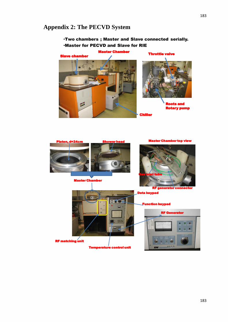
183
183
Appendix 2: The PECVD System
•Two chambers ; Master and Slave connected serially.
•Master for PECVD and Slave for RIE
Master Chamber
Slave chamber
Chiller
Roots and
Rotary pump
Throttle valve
Shower headPlaten, d=24cm
Master Chamber
Data keypad
Function keypad
RF Generator
RF matching unit
Temperature control unit
Gas inlet tube
RF generator connector
Master Chamber top view

184
184
Appendix 3: Supplementary AFM DATA
90 nm
180 nm
Figure 0-1: AFM micrograph of silicon film grown at 300 °C on NFD-coated
substrate. The surface grain are observed to be elliptical with dimensions of
~180 X 90 nm
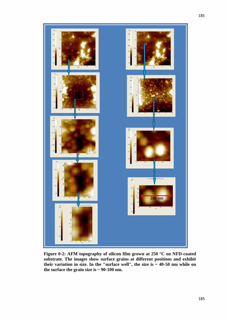
185
185
280 nm
Figure 0-2: AFM topography of silicon film grown at 250 °C on NFD-coated
substrate. The images show surface grains at different positions and exhibit
their variation in size. In the "surface well", the size is ~ 40-50 nm while on
the surface the grain size is ~ 90-100 nm.