a multiport page-memory architecture and a multiport disk-cache system
TRANSCRIPT
New Generation Computing, 2 (1984) 241-260 OHMSHA,LTD. and Springer-Verlag
�9 OHMSHA, LTD. 1984
A Multiport Page-Memory Architecture and A Multiport Disk-Cache System
Yuzuru T A N A K A
Department of Electrical Engineering, Hokkaido University, Sapporo 060, Japan
Received 28 May 1984
A b s t r a c t Everlasting demands for solutions to ever growing computation problems and demands for efficient means to manage and utilize sophisticated information have caused an increase in the amount of data necessary,to handle a job, while drastic reduction in CPU prices is encouraging massive parallel architectures foE gigantic data processing. These trends are increasing the importance of a large shared buffer memory with 103--10 4 simultaneously accessible ports. This paper proposes a multiport page buffer architecture that allows 10 3_ l0 4 concurrent accesses and causes no access conflict nor suspension. It consists of a set of memory banks and multistaged switching networks with controllers that control each row of the networks. Consecutive words in each page are stored orthogonal- ly across banks. Memory interleaving may be applied to improve access rate in consecutive retrievals. When used as a disk cache memory, it decreases the number of disk accesses and increases both the page transfer rate and the maximum number of concurrent page accesses.
Keywords:Memory Architecture, Shared Memory, Disk Cache, Multiprocessor, Database Machine
w 1 In troduct ion Everlasting demands for so lu t ions to ever growing c ompu t a t i on problems
and demands for an efficient means to manage and utilize sophist icated informa-
t ion have caused an increase in the a m o u n t of data necessary to handle a job.
Demands for more accurate so lu t ions to three d imens iona l mesh problems are
not satisfied by current pr imary memory super computers. To meet these
demands, disk storage in coopera t ion with a primary memory is necessary to
242 Y. Tanaka
provide a sufficiently large memory, however, frequent disk access results in loss of computer efficiency.
The situation is similar to that found in database machine research and development. Database machine research efforts are now confronted with "Disk Paradox' as pointed out by H. Boral and D. J. Dewitt in 1983. ~) Obviously, the number of disk units necessary to store a database is inversely proport ional to the capacity of a single disk unit. Hence, the maximum outflow obtainable from a set of disk units is proport ional to the transfer rate of a single unit, and inversely proport ional to its capacity. On the other hand, the current develop- ment effort is directed toward increasing disk capacity with little improvement or even deterioration in transfer rate. This lowers the maximum outflow from the secondary memory, which bounds machine performance and nullifies massive parallel processing. Historically, this kind of problem has been re- petitively encountered, and resolved through the combinat ion of two techni- ques : A buffer memory placed between the primary memory and the secondary memory not only resolves the gap in access speed but also decreases secondary memory access frequency while data clustering into segments increases access locality and enhances buffer effects.
Drastic reduction in CPU prices is further encouraging massive parallel architectures for gigantic data processing both in numerical computat ions and in nonnumerical computat ions. The buffer used in interfacing a bunch of processors to a set of disk units must have enough ports to allow simultaneous data transfer to and from the processors and the disk units. Technological trends will soon make it realistic to have ]0 2 - l0 4 processors work in parallel. Shared buffer design should take into account the capabil i ty to increase the number of ports to 10 3_ 10 4 to cope with future innovative computer systems. Technology will soon allow parallel used 10 3_ I0 5 processors.
Obviously, this design goal is very hard to achieve. Even a 10-port memory designed to work without any access conflict or suspension is difficult to realize. The answer to these difficulties lies in the observation that the shared buffer we are going to design does not necessarily provide random accessibility of every word. Actually, what we want is a page-buffer memory that allows random single page access. Besides, a page is not necessarily accessible unless its transfer is completed. This property gives us a clue to the solution of these architectural difficulties, Multiport page buffer architectures proposed in this paper physically allows simultaneous access from all ports without causing any conflict among them nor any suspension. Read accesses cause no logical problem even if they are simultaneously executed. The involvement of more than one write access, however, might cause logical inconsistency. Some kind of coordination, either through software or hardware, is necessary to control concurrent access.
The buffer should be no slower than a low-speed semiconductor RAM. It should be able to connect different ports to various devices of different speed.

A Multiport Page-Memory Architecture and A Multiport Disk-Cache System 243
When used as a disk cache memory, the access port speed should be equal to processor memories, or at least half as fast, while other ports connected to disk units should be accessible in synchronization with their rotation.
Shared page-buffer architecture proposed in this paper satisfies all of the above mentioned requirements. Besides, its implementation is feasible with current technologies. It consists of networks and a set of memory banks. Banks
need no special memory architecture but currently available MOS RAM chips, while the networks seem feasible within the scope of current technologies.
The introduction of a shared page-buffer located between a bunch of processors and a set of disk units requires automatic translation of page addresses, which must be consistent among different ports. The maintenance of
address consistency by software is not only difficult from a logical point of view but also causes serious overhead. Therefore, use of a shared page-buffer, when used as a disk cache memory, is desired to be accompanied by a hardware address
translator. This topic will be discussed in Section 3. Such extension enables the processors to view a shared page-buffer that is backed up by a set of disk units
as a one-level storage system for page random access.
w 2 Multiport Page-Buffer Memory
2. 1 Basic Architecture Common sense tells us that a shared memory with 103~104 ports
operating in a conflict-free manner is unrealistic, and will not be feasible even
in the future. Application to a page-buffer, however, would make it possible even with current technologies to provide a buffer with a sufficiently large
number of concurrently accessible ports. A shared memory typically has an architecture as shown in Fig. I. 3) It
consists of a set of memory banks and a bilateral communication network. Simultaneous accesses of the same word from different ports causes conflict in a network, which works as an arbitrator to resolve such conflicts. When conflict
occurs, only one of the ports involved is given acknowledgement. Others are forced either to retry their accesses or to wait in a queue installed in the network.
A set of banks has two alternative word arrangements. Consecutive words might be arranged either vertically in a single bank or horizontally across banks.
The latter orthogonal arrangement known as memory interleave has been used to speed up a single port memory system.
A page memory divides its memory space into fixed number consecutive
word segments. Suppose that a multiport page-buffer has basically the same configuration as shown in Fig. 1. If each page is stored vertically in a single memory bank, concurrent accesses to the same page inevitably causes a conflict in the network. Orthogonal arrangement of each page resolves this problem.
The page size S is assumed to be a multiple of the number of ports n. Word address in a page buffer is denoted by a pair (p, d) ; p is a page number
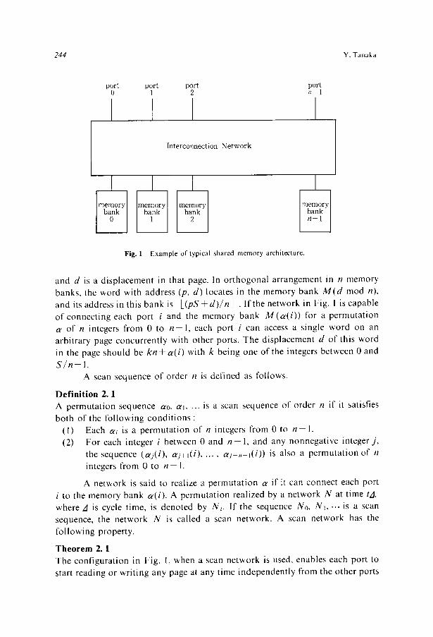
244 Y. Tanaka
port port port port 0 1 2 z* 1
Interconnection Network
Fig. 1 Example of typical shared memory architecture.
and d is a displacement in that page. In o r thogona l arrangement in n memory
banks, the word with address (p, d) locates in the memory bank M ( d mod n), and its address in this bank is L ( p S + d ) / n J . If the network in Fig. 1 is capable
o f connect ing each port i and the memory bank M ( a ( i ) ) for a permutat ion a o f n integers from 0 to n - l , each port i can access a single word on an arbitrary page concurrent ly with other ports. The displacement d o f this word in the page should be k n + a ( i ) with k being one o f the integers between 0 and
S / n - 1 . A scan sequence o f order n is defined as follows.
Definition 2. 1 A permutat ion sequence a0, at . . . . is a scan sequence o f order n if it satisfies
both of the fo l lowing condi t ions : (1) Each ai is a permuta t ion o f n integers from 0 to n - 1 . (2) For each integer i between 0 and n - - 1, and any nonnegat ive integer j ,
the sequence (a j ( i ) , a j+ l ( i ) . . . . . aj+, i(i)) is also a permuta t ion of n
integers from 0 to n - -1 .
A network is said to realize a permutat ion a if it can connect each port
i to the memory bank a(i) . A permutat ion realized by a network N at time tA, where zl is cycle time, is denoted by Nt. If the sequence No, N~, ... is a scan sequence, the network N is called a scan network. A scan network has the
fol lowing property.
T h e o r e m 2. 1 The configurat ion in Fig. I, when a scan network is used, enables each port to start reading or writing any page at any time independent ly from the other ports
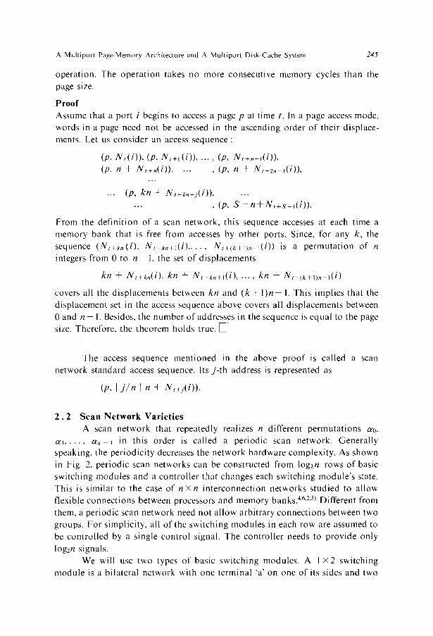
A Multiport Page-Memory Architecture and A Multiport Disk-Cache System 245
opera t ion . The o p e r a t i o n takes no more consecut ive memory cycles than the
page size.
Proof Assume that a por t i begins to access a page p at t ime t. In a page access mode,
words in a page need not be accessed in the ascending order o f their d i sp lace-
ments. Let us cons ide r an access s equence ;
(p, N , ( i ) ) , (p, N t + t ( i ) ) . . . . . (p, N , + n ,(i)) ,
(p, n + N , + , ( i ) ) . . . . , (p, n + Nt+2,, i(i)), . . .
... (p, k n + Nt+kn+j( i ) ) . . . .
�9 .. , (p, S - - n + N ~ + s i(i)).
From the de f in i t ion o f a scan ne twork , this sequence accesses at each t ime a
memory bank that is free from accesses by o ther ports . Since, for any k, the
sequence ( N t + ~ n ( i ) , N , + k , + j ( i ) . . . . . N t+(k~ l ) , 1(0) is a p e r m u t a t i o n of n
integers from 0 to n 1, the set o f d i sp l acemen t s
k n + N t + k , ( i ) , kn + Nt+k~+j( i ) . . . . . kn + N t + ( k + o , , - l ( i )
covers all the d i sp lacemen t s between k n and ( k + l ) n 1. This impl ies that the
d i sp lacement set in the access sequence above covers all d i sp lacement s between
0 and n - I. Besides, the number o f addresses in the sequence is equal to the page
size. Therefore, the theorem holds true. ~ ]
The access sequence men t ioned in the above p r o o f is ca l led a scan
ne twork s t andard access sequence. Its j - t h address is represented as
(p, L j / n j n + Nt+9(i)) .
2 . 2 Scan N e t w o r k Variet ies A scan ne twork that repea ted ly real izes n different pe rmu ta t i ons a0,
a~ . . . . . a,, t in this o rde r is ca l led a pe r iod ic scan ne twork . Gene ra l ly
speaking, the pe r iod ic i t y decreases the ne twork ha rdware complex i ty . As shown
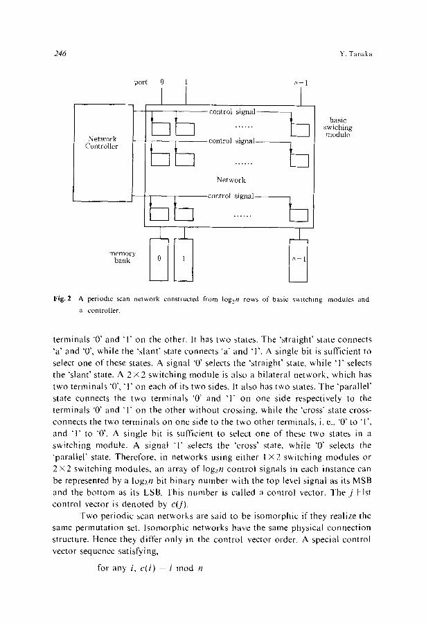
in Fig. 2, pe r iod ic scan ne tworks can be cons t ruc ted from log2n rows o f basic
swi tching modu les and a con t ro l l e r that changes each swi tch ing modu le ' s state.
This is s imi la r to the case o f n • in te rconnec t ion ne tworks s tud ied to a l low
flexible connec t ions between processors and memory banks. 4,6,2,5) Different from
them, a per iod ic scan ne twork need not a l low a rb i t ra ry connec t i ons between two
groups. Fo r s impl ic i ty , all o f the swi tch ing modu le s in each row are assumed to
be con t ro l l ed by a s ingle con t ro l signal. The con t ro l l e r needs to p rov ide only
log2n signals.
We will use two types o f basic swi tch ing modules . A I X 2 swi tching
modu le is a b i la te ra l ne twork with one te rmina l "a' on one of its sides and two
246 Y. Tanaka
Fig. 2
port
Network Controller
memory bank
0 1 /~- 1
I I [
Network
~ - ' ] ~ " l cOntrOl I I~I1
basic swiching module
A periodic scan network constructed from Iog2n rows of basic switching modules and a controller.
terminals '0 ' and 'l" on the other. It has two states. The "straight' state connects
'a ' and "0', while the "slant' state connects 'a" and '1'. A single bit is sufficient to select one o f these states. A signal '0 ' selects the "straight' state, while '1 ' selects the "slant' state. A 2 x 2 switching module is also a bilateral network, which has two terminals '0', '1' on each of its two sides. It also has two states. The 'parallel ' state connects the two terminals "0' and ~[" on one side respectively to the
terminals '0 ' and "1" on the other without crossing, while the 'cross" state cross- connects the two terminals on one side to the two other terminals, i. e., "0' to '1", and "l' to '0'. A single bit is sufficient to select one of these two states in a
switching module. A signal "1' selects the 'cross ' state, while '0' selects the "parallel' state. Therefore, in networks using either I x 2 switching modules or 2 X 2 switching modules, an array o f Iog2n control signals in each instance can be represented by a log2n bit binary number with the top level signal as its MSB
and the bot tom as its LSB. This number is called a control vector. The j + l s t control vector is denoted by c(j).
Two periodic scan networks are said to be isomorphic if they realize the same permutat ion set. I somorphic networks have the same physical connect ion structure. Hence they differ only in the control vector order. A special control vector sequence satisfying,
for any i, c(i) i rood n

A Multiport Page-Memory Architecture and A Multiport Disk-Cache System 247
is ca l led the regula r sequence o f con t ro l vectors. In the sequel , every cont ro l
vector sequence is regarded as regular . A m o n g pe r iod ic scan ne tworks , the
fo l lowing two types are worth ment ion ing . The number o f por ts is assumed to
be a power o f two.
( I ) A rotary ne twork
Nj ( i ) = i + j mod n
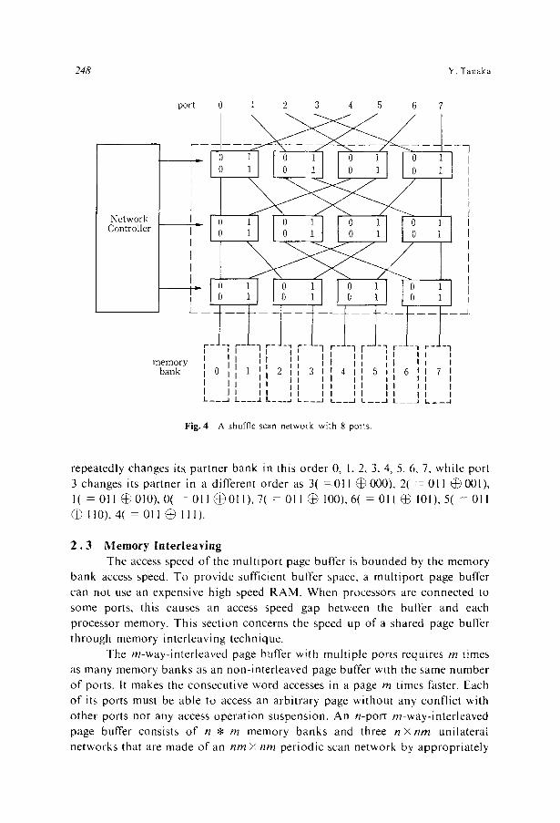
(2) A shuffle scan ne twork
N j ( i ) = i @ ( j mod n),
where i @ j is a bi twise exclusive OR of i and j .
A rotary ne twork uses I X 2 switch modules , and has a c onne c t i on pat tern
as shown in Fig. 3. The con t ro l l e r repea ted ly sends a sequence o f con t ro l vectors
port 0 1 2 3 4 5 6 7
Network Controller
Fig. 3 A rotary network with 8 ports.
0, 1, 2 . . . . . n - - 1 in this order . A por t i r epea ted ly changes its pa r tne r bank
incrementa l ly from i to n - - 1, and then from 0 to i - 1. A shuffle scan ne twork
uses 2 • switch modules , and has a different connec t ion pat tern as shown in
Fig. 4. This pat tern i tself is well k n o w n as a shuff le-exchange ne twork , or more
precisely, omega ne twork . 41 Its con t ro l l e r also sends a con t ro l vector sequence 0,
1, 2 . . . . . n 1 in this order . The j - t h pa r tne r o f por t i is de t e rmined by the
bi twise exclusive OR o f i and (j' I rood n). Fo r n - 8, por t 0, for example ,
248 Y. Tanaka
port 0 i 2 3 4 5 6 7
I I I J
Network [ Controller I
I
I I I - - - - m J L_.
memory bank
, JJ j l ] i i i j r i l l i i ] ] I I I I I I I I [ I I ] I I k__..-I k - - - J L .... ..a L--_-.I L__..--I L__.-I L__o, L___.-I
F i g . 4 A shu f f l e s c a n n e t w o r k w i t h 8 p o r t s .
repeatedly changes its partner bank in this order 0, 1, 2, 3, 4, 5, 6, 7, while port 3 changes its partner in a different order as 3 ( = 0 1 1 @ 0 0 0 ) , 2( = 011 @001) ,
I( = 0 1 1 @ 0 1 0 ) , 0 ( = 0 1 1 @ 0 1 1 ) , 7 ( = 0 1 1 @ 1 0 0 ) , 6 ( = 0 1 1 @ 1 0 1 ) , 5 ( = 0 1 1 @ ] 1 0 ) , 4( - 0 1 1 @ 1 1 1 ) .
2 . 3 M e m o r y In t e r l e a v i ng
The access speed o f the mult iport page buffer is bounded by the memory bank access speed. To provide sufficient buffer space, a mult iport page buffer can not use an expensive high speed RAM. When processors are connected to
some ports, this causes an access speed gap between the buffer and each processor memory. This section concerns the speed up of a shared page buffer through memory interleaving technique.
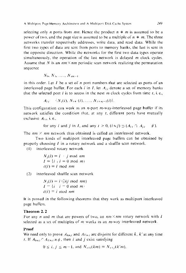
The m-way-inter leaved page buffer with multiple ports requires m times as many memory banks as an non-interleaved page buffer with the same number o f ports. It makes the consecutive word accesses in a page m times faster. Each
of its ports must be able to access an arbitrary page without any conflict with other ports nor any access operat ion suspension. An n-port m-way-inter leaved
page buffer consists o f n * m memory banks and three n • unilateral networks that are made o f an n m • nrn periodic scan network by appropr ia te ly
A Muhiporl Page-Memory Architecture and A Multiport Disk-Cache Syslem 249
selecting only n por t s from nrn. Hence the p roduc t n * rn is assumed to be a
power o f two, and the page size is assumed to be a mul t ip le of n * m. The three
ne tworks transfer respect ively addresses, wr i te data, and read data . W h i l e the
first two types o f d a t a are sent from por ts to memory banks , the last is sent in
the oppos i t e d i rec t ion . Whi le the ne tworks for the first two da t a types opera te
s imul taneous ly , the ope ra t i on of the last ne twork is de layed rn c lock cycles.
Assume that N is an nrn • n m per iod ic scan ne twork rea l iz ing the pe rmuta t ion
sequence
No, N i . . . . . N n,,- i
in this order. Let 1 be a set o f n por t numbers that are selected as por ts o f an
inter leaved page buffer. Fo r each i in 1, let Ai, t denote a set o f memory banks
that the selected por t i is to access in the next rn c lock cycles f rom t ime t, i. e.,
At,, - {N, ( i ) , Nt+l ( i ) . . . . . N t + m I(i)}.
This conf igura t ion can work as an n -por t m-way- in te r l eaved page buffer if its
ne twork satisfies the c o n d i t i o n that , at any t, different por ts have mutua l ly
exclusive At,t , i. e.,
for any i and j in 1, and any t > O, ( i ~ j ) D (Ai,t 0 Aj , t - - ~ ).
The nrn • nrn ne twork thus ob t a ined is ca l led an in ter leaved ne twork .
Two kinds o f mu l t i po r t in ter leaved page buffers can be o b t a i n e d by
proper ly choos ing 1 in a ro tary ne twork and a shuffle scan ne twork .
( I ) in ter leaved ro tary ne twork
N j ( i ) - i + j mod n m
1 = { i l i - O m o d m}
c ( i ) - i rood n m
(2) in ter leaved shuffle scan ne twork
N j ( i ) - i @ ( j rood n m )
I - {i I i - - O rood m} c ( i ) - i rood n m
It is proved in the fo l l owing theorems that they work as m u l t i p o r t in ter leaved
page buffers.
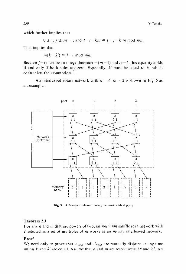
Theorem 2. 2 F o r any n and rn that are powers o f two, an n r n X n r n ro tary ne twork with 1
selected as a set o f mul t ip les o f rn works as an m-way in te r leaved ne twork .
Proof We need on ly to p rove Akm,t and ml~m,t a re d i s jo in t for different k , k ' a t any t ime
t. [ f Akm,t N Ak'm,t:~?~, then i and j exist sat isfying
0 _< i, j < m - l , and N ~ + i ( k m ) = N t + j ( k ' m ) ,
250 Y. Tanaka
which further implies that
0 < i , j < m - - l , and t + i + k m = t + j + k ' m rood n m .
This implies that
m ( k - k ') = j - i rood n m .
Because j - i must be an integer between - ( m - 1) and m - 1, this equa l i ty holds
if and only if both sides are zero. Especially, k ' must be equal to k, wilich
contradicts the assumpt ion . [ ]
An interleaved rotary network with n -- 4, m = 2 is shown in Fig. 5 as
an example.
Network Controller
port 0 i 2 3
~- a-
I
a
[
-] I I
I , f a l l , , , , momory , 0 ' , 1 ' , ' , 2 , , , 4 ' 5 , G , '7 ' , bank I I e l I I I I u
I I I I I I I I I II L - - - - - a L - - - ~ J L - - - - I L - - J L - - - - I - - - a L _ - - J L - - - - J
Fig. 5 A 2-way- in te r leaved r o t a r y ne twork with 4 ports .
T h e o r e m 2.3 For any n and m that are powers of two, an n m • n m shuffle scan network with
1 selected as a set of mul t ip les of m works as an m-way interleaved network.
P r o o f We need only to prove that Akm.t and Ak',,,.t are mutua l ly d is jo in t at any time
unless k and k ' a r e equal . Assume that n and m are respectively 2 a and 2b. An
A Multiport Page-Memory Architecture and A Multiport Disk-Cache System 25]
element o f Ak,,,,, has the general form
k l k 2 . . . k a O 0 . . . O @ t l t z . . . t a t ~ + l , , . t~+b,
b
where k ~ k 2 . . , k~ is a bir~zry represen ta t ion o f k, and t i t 2 .-- t~+~ is a b ina ry
number belween 0 and n m 1. If Ak,~s and Akin,, are no1 d i s jo in t , i and j exisl such t h a l
t _< i, j < t + m, and N i ( k m ) = N j ( U m ) ,
which further impl ies that
t <_ i , j < _ t + m, and
( k l k2 . . . k a 0 0 . . . O ) @ ( i l i 2 . . . i a+b)
b
= ( k ' l k ' 2 . . . k ' a O 0 " " 0 ) @ ( j l j 2 . . . j a + b ) .
b Therefore, the last b bits o f i must be equal to the same po r t i on o f j , i.e., i -
j rood m. Let i ' and j ' respectively deno te ( i - - t ) and ( j - - t ) . It must ho ld that
O < _ i ' , j ' < m .
Since it holds that
t + i ' - i - j = t + j ' m o d m,
i ' must be congruen t to j ' m o d u l o m. This impl ies that i" = 1 ' Hence i( = t +
i ') is equal to j ( - t + j ' ) . Since it ho lds that
k i n @ i - k ' m @ j and i = j ,
it car~ be conc luded that k = k ' . Th i s c~ntradic~s the a s s u m p : i o m T~erefore
A,,,., arid A~.,,, must be d i s jo in t for differenl k , k ' .
An in ter leaved shuffle scan ne twork with n = 4 and m = 2 is shown in
Fig. 6.
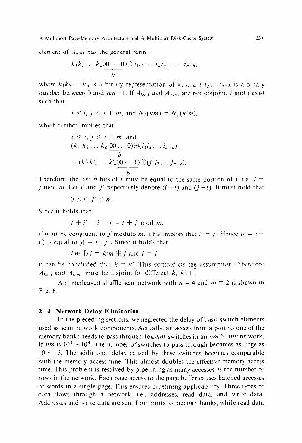
2 . 4 Network Delay Elimination In the p reced ing sections, we neglected the delay o f basic switch e lements
used as scan ne twork componen t s . Ac tua l ly , an access from a por t to one o f the
memory banks needs to pass th rough l o g 2 n m switches in an n m • n m network.
If n m is 103 -- 104 , the number o f switches to pass th rough becomes as large as
1 0 - 13. The a d d i t i o n a l de lay caused by these switches becomes c o m p a r a b l e
with the memory access time. This a lmost doub le s the effective memory access
time. This p rob l em is resolved by p i p e l i n i n g as many accesses as the number o f
rows in the ne twork . Each page access to the page buffer causes ha tched accesses
o f words in a s ingle page. This ensures p i p e l i n i n g app l i cab i l i t y . Three types o f
da t a flows th rough a network, i.e., addresses, read data , and write data.
Addresses and wri te da ta are sent from por ts to memory banks , whi le read da ta

252 Y. Tanaka
Network Controller
memory bank
port 1 2
1 0
1 0
\ 0 l i fo rp0 0 1 0 1 0
4 ~ I
I i I I I I I I I IJ ,~ ,~ L _ _ _ L _ _ - L _ _ J L _ _ - . I L _ _ J L _
3
/
r \ 1 lifo o 1 i
I I ""1 f t I i I i I
G I 7 , I i I I I I I I I I I I I I I
L _ _ a L . _ _ J . _ _ _ 1
F i g . 6 A 2-way-interleaved shuffle scan network with 4 ports.
is sent in the opposite direction. This access pipelining uses a dedicated unilateral network for each of the three data types. In each network, every value
proceeds from one row to the next in every clock cycle. Each basic switch element may be unilateral. It is provided with a register to store a value.
In the networks for addresses and write data, the first row from ports
should be controlled first, and control of the second row should come next. The sequence of such control can be implemented by sending the network a sequence of control vectors in a skewed arrangement, i.e., the i-th most significant bit of
the j-th control vector is set equal to the i-th bit of the log2nm bit representa- tion of the integer j - - i . This is illustrated in Fig. 7. Similarly, in the network for read data, the first row from memory banks should be controlled first. Hence, i-th least significant bit of the j-th control vector is set equal to the i-th least
significant bit of integer j - i . This is also illustrated in Fig. 7. Since the sending of a read out value through a network should be
preceded by both the sending of its address from a processor to a memory bank and the memory read operation, read data network control should be delayed for log2nm § rn clock cycles behind the control of the two other networks. This is illustrated in Fig. 7. Memory bank access time should be no more than m
clock cycles.
A Multiport Page-Memory Architecture and A Multiport Disk-Cache System 253
il
j - - i
\
J
Control ler
1 m j log2nra
N e t w o r k j Control ler
port 0 1 2 3
r' 1
1
~ 1 ( , 1 11
r - "
mem~ I 0 I I ] ' l 2 II 3 II 4 l ' 5 I[ 6 I 1 7 1 bank , , I ] ! ~, ' I ' I , ~ , ' '
L - - - - J L - - - - J k - - - - J L _ _ - I L - - - J L - - - - J L - - _ J L - - - - J
(a) Address N e t w o r k / W r i t e Data N e t w o r k
port 0 1 2 3
_ - - 4
I I I m e m o r y , , , I I I I I ' I , I I ' t t , 0 , ~ 1 , 2 3 , 1 4 , 1 5 1 v 6 t l 7 I bank , I ' , 'l , ] l , ' , ,
L__J k__J L_-J L__J --__J L - - - - ~ L - - - - J L - - - - J
(b) Read Data N e t w o r k
Fig. 7 Pipelined unilateral networks with different directions.
w 3 Multiport Disk Cache Memory
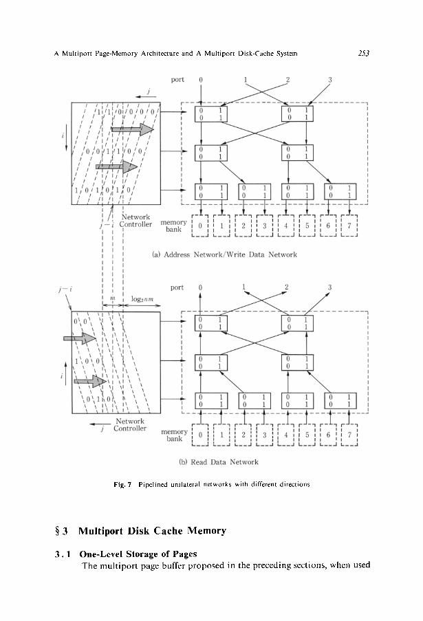
3.1 One-Level Storage of Pages The multiport page buffer proposed in the preceding sections, when used

254 Y. Yanaka
with a set o f disk units, can construct a one-level shared storage o f pages. It provides us with a huge virtual memory space divided into pages. Each page is
given a unique page address so that it may be directly accessible. The mult iport page buffer and some addit ional circuits works as a mult iport disk cache memory as shown in Fig. 8. Mult iport page buffer ports are divided into two
groups. Each port in the first g roup is assigned to a processor, while each in the second group is assigned to a disk control ler with one or more disk drive units. The functions o f a mul t ipor t disk cache memory are similar to those of cache memories that are used to improve the main memory access time. It a lways stores
a fixed number o f the most recently accessed pages in a semiconduc tor memory in order to decrease repetitive disk accesses to the same page requested not only by the same processor but also by different processors. Commerc ia l ly available disk cache systems today have no such funct ions as fixed number automat ic
staging of the most recently accessed pages in a buffer, nor au tomat ic address translation from a logical address to a physical address in the staging buffer.
address
Priority Update List for Replacement
control Control
Directory
O - - Processor Pool ~ Multiport
Page- Memory
0 - -
:1 ] Switch ]
I I
k_ . . . . .
Disk Array
Fig. 8 Configuration of a multiport disk cache.
A Muhiport Page-Memory Architecture and A Muhiport Disk-Cache System 255
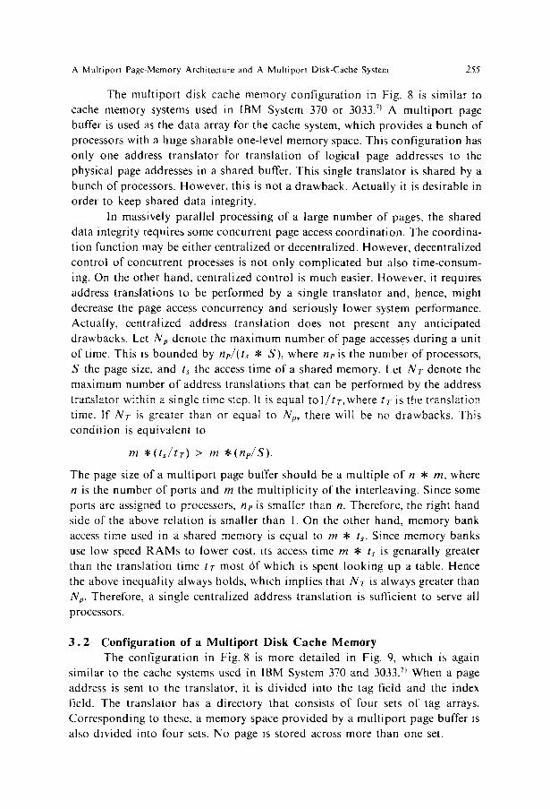
The multiport disk cache memory configuration in Fig. 8 is similar to cache memory systems used in IBM System 370 or 3033. 71 A multiport page buffer is used as the data array for the cache system, which provides a bunch of processors with a huge sharable one-level memory space. This configuration has only one address translator for translation of logical page addresses to the physical page addresses in a shared buffer. This single translator is shared by a bunch of processors. However, this is not a drawback. Actually it is desirable in order to keep shared data integrity.
In massively parallel processing of a large number of pages, the shared data integrity requires some concurrent page access coordination. The coordina- tion function may be either centralized or decentralized. However, decentralized control of concurrent processes is not only complicated but also time-consum- ing. On the other hand, centralized control is much easier. However, it requires address translations to be performed by a single translator and, hence, might decrease the page access concurrency and seriously lower system performance. Actua[ly, centralized address translation does not present any anticipated drawbacks. Let Np denote the maximum number of page accesses during a unit of time. This is bounded by n e / ( t , * S ) , where ne is the number of processors, S the page size, and t, the access time of a shared memory. Let N r denote the maximum number of address translations that can be performed by the address translator within a single time step. It is equal t o l / t r , where t r is the translation time. tf N r is greater than or equal to Np, there wilt be no drawbacks. This condition is equivalent to
m * ( t , / t r ) >_ m * ( n e / S ) .
The page size o f a multiport page buffer should be a multiple of n * m, where n is the number of ports and m the multiplicity of the interleaving. Since some ports are assigned to processors, ne is smaller than n. Therefore, the right hand side of the above relation is smaller than 1. On the other hand, memory bank access time used in a shared memory is equal to m * ts. Since memory banks use low speed RAMs to lower cost, its access time m * ts is genarally greater than the translation time t r most of which is spent looking up a table. Hence the above inequality always holds, which implies that N r is always greater than Np. Therefore, a single centralized address translation is sufficient to serve all processors.
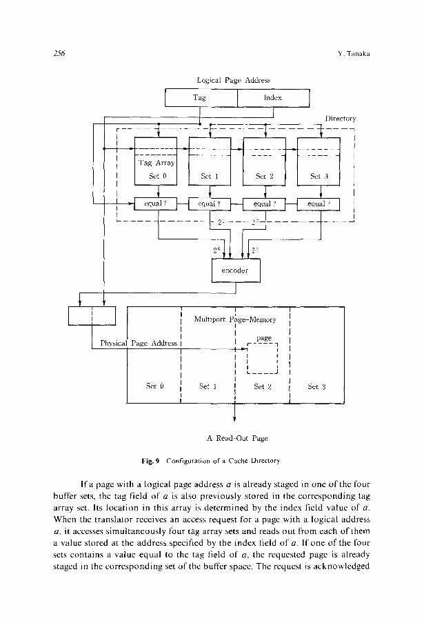
3 . 2 Configuration of a Multiport Disk Cache Memory The configuration in Fig. 8 is more detailed in Fig. 9, which is again
similar to the cache systems used in IBM System 370 and 3033. 7) When a page address is sent to the translator, it is divided into the tag field and the index field. The translator has a directory that consists o f four sets of tag arrays, Corresponding to these, a memory space provided by a multiport page buffer is also divided into four sets. No page is stored across more than one set.
256 Y. Tanaka
I _ _
r
Logical Page Address
f Tag I Index ]
~ Tag Array~-~ ~ - - - ~ ~ - - - - ~ ~---~ iy
equal ? [---[ equal ? ]---[ equal ? ] ~ . eq
I
Physical Page Address
1 b
Multiport Page-Memory I
I page I r - . . . . -I
I I J I J
I J j L . . . . J I
Set 0 Set i I I
Set 2 Set 3
A Read-Out Page
Fig. 9 Configuration of a Cache Directory.
Ira page with a logical page address a is already staged in one of the four buffer sets, the tag field of a is also previously stored in the corresponding tag array set. Its location in this array is determined by the index field value of a. When the translator receives an access request for a page with a logical address a, it accesses simultaneously four tag array sets and reads out from each of them a value stored at the address specified by the index field of a. If one of the four sets contains a value equal to the tag field of a, the requested page is already staged in the corresponding set of the buffer space. The request is acknowledged
A Muhiporl Page-Memory Architecture and A Multiport Disk-Cache System 257
immediately and the set number is sent back to the requesting processor, which will be able to directly access the desired page staged at the physical page address specified by the concatenat ion o f the selected set number and the index field of a. Otherwise, the requested page must be read out from one of the disk
units to be staged in ~he buffer. This disk unit is calculated from the logical address a. The read out page is stored in one o f the four sets o f buffer space. Its physical location in this set is determined by the logical address index field.
If, in every set, this location is already occupied by another page, we have
to choose one page out o f four to replace it with the read out page. The least recently used page is selected from a m o n g the four old pages. For this selection, the directory is provided with a priority queue for each of its addresses. For space efficiency, the states o f these queues are encoded and a decoding circuit is
provided for the directory. Implementa t ion o f this part may use the same technique as is used in cache systems o f main frame computers . When an old page is replaced by a new page, the old page is restored in its home disk unit,
and, in the selected set, the tag field o f the logical page address o f the new page is written in the tag array, at the locat ion specified by the index field. After these
operations, the access request will be acknowledged.
3 . 3 Interfacing Disk Units to the Shared Page Buffer Each mul t ipor t page buffer port has a constant access rate that is the
inverse o f the clock cycle. Let N be a per iodic scan network and p an integer
that is prime to nrn. Then it is obvious that No, Np, N2p . . . . . N(,~,~_ 0~,, N,,~p . . . . is also a periodic scan sequence. Therefore, any page can be accessed from any port at an l / p access rate if and only if p is either one or an integer prime to nm. However, the access rate o f a disk unit and that o f the shared page buffer is not aIways mutual ly prime. Some devices can not transfer data without
f luctuations occur ing in transfer rates. However , the consecutive accesses to the shared page buffer does not al low access rate fluctuations, Besides, some devices
such as disk units can not start page read/wri te operat ion arbitrarily. Some other devices can not access words on a page in an arbitrary order. Since the port i of the shared buffer can access at t ime t a word at a displacement kn + Nt(i) for some integer k, these devices can not be directly connected to the shared
buffer. These problems are solved by in t roducing two n * m word buffers
between such devices and the shared page buffer port. Two buffers are used alternately. While one o f them is receiving fol lowing n * m words from either
the device or the shared buffer, the other buffer is sending the last received n m words to the other system. Since the shared page buffer transfer rate is much faster than the device transfer rate, the transfer o f a page to and from the shared page buffer has to wait for one o f the buffers to be filled up or be emptied after every n * m word transfer, if the buffers are considered as a part o f such a device, the delay introduced by this interface is no more than n * m clock
258 Y. Tanaka
cycles, which is independent from the page size and much smaller than the transfer time for a single page.
w 4 Conclusion The mult iport page buffer architecture proposed in this paper provides a
new type o f a shared storage space for massive parallel processing, it can afford 10 3 ~ l0 4 ports each o f which can read or write an arbitrary page in the shared space without any confl ict nor any wait. It consists o f three unilateral networks,
two network control lers that sequentially provide the networks with control vectors, and a set o f memory banks.
An m-way-inter leaved shared page buffer with n ports uses n * m
memory banks and n • nm interleaved networks each of which is made of an n m • nm network by appropr ia te ly choos ing n ports from nm. If each memory
bank uses RAM chips with access time tb, each port can access m / t b words in a single time unit. A l though communica t ion through a network causes some addit ional delay p ropor t iona l to the number o f switching module rows in the
network, consecutive access pipelining can eliminate this delay which effects access rate. The page size o f a shared page buffer is selected as a mult iple o f n �9 m. Let it be k * n * m, where k is a natural number. The max imum number
o f page accesses a l lowed for each port in a single unit o f time is determined by m / ( t b * S) , which is equal to l / ( k * tb * n). The maximum number o f pages accessible by a bunch o f ports is n times as large as this, i.e., l / k * tb. For tb = 10 -6 sec, it becomes ( l / k ) 1 0 6 pages/sec. For n = 1 000, m = 1, and S = 10K
words, this results in 10 5 pages/sec, which is sufficiently large.
When used as a disk cache memory, the shared page memory architecture provides a bunch o f processors with a huge one-level shared storage space that is actually backed by a set o f disk units. The ports o f the shared page buffer are
divided into two groups. One is assigned to processors, while the other is assigned to disk units. Each page in the virtual space is given a un ique logical
page address. The shared page buffer stores a fixed number o f page copies to speed up repetitive use o f them by processors. When a page requested by a processor is not already staged in the buffer, it is read out from one o f the disk units and stored at a proper location in the buffer. Each locat ion in the buffer
has a physical address. Therefore, the staging o f a new page in the buffer needs translation from its logical address to a physical address. This is performed by a single address translator. All requests by processors are sent to this t ranslator and processed there. This centralization, however, does not cause any bottle-
neck. Let np be the number o f processors and nD that o f the disk units. Obvi- ously, n p + n D is n. Let t r be the address translat ion time. Then the maxi- mum number of page requests by processors in a single unit o f time is no more
than n p / ( k * tb * n) ( = np * m / ( t b * S)), while the number o f t ranslat ions that can be performed in a single unit o f t i m e i s l / tT . The latter is R * ( n / n p )
�9 ( t b / t r ) t i m e s faster than the former. This number is, in a practical si tuation,

A Multiport Page-Memory Architecture and A Multiport Disk-Cache System 259
always greater than one. Therefore, the centralization of the address translation does not result in any drawbacks.
Let to be the average access time of a disk unit and to' be the time necessary for the transfer of one word to and from a disk unit. Then the maximum number of pages directly accessible from a set of disk units is no /
( t o + k * n * m * t o ' ) . Assume that the disk cache capacity is sufficient, and that pages are frequently repetitively used while they are stored in the buffer. Then the page hit ratio in the buffer is close to one. In such a case, introduction of a multiport disk cache memory improves the maximum number of possible page accesses in a single unit of time by
(ne * ( t o + k * n * m * t D ' ) ) / ( n o * k * tb * n)
times. As a typical case, consider the following example,
disk access time ( to) : 30 msec,
transfer time for a word to and from a disk unit (to') : 1 microsec, memory bank access time (tb) : 200 nsec, number of ports (n) : I 0 3 interleaving multiplicity (m) : 10, page s ize / (n , rn) (k) : 2, number of processors (np) : 900, number of disk controllers (riD) : 100.
Then the improvement rate above becomes approximately l03. This is large enough to encourage massive parallel processing architectures that deal with large amounts of data.
Among the various fields in which such memory architecture can be applied, database machines are the most worth mentioning. Multiport disk cache architecture will raise alleged possible parallelism boundaries caused by 'Disk Paradox'. This is based on the prediction that one page of a directory or a relation in a database is frequently repetitively used. This prediction is accepted by two reasons. Complicated transactions often require one page to be seen repetitively. An example is the nested loop algorithm used to join two relations each of which is segmented into pages. Besides, it seems probable that the focus of user attention in a shared database, when observed during a day, a week, or a month, is likely to overlap with other users' attention. However, it can be hardly specified which portion of a database is receiving most of their attention. A multiport disk cache system can automatically stage hot pages in itself. Our research is now directed toward massive parallel database machine architecture using this multiport disk cache architecture. This will be reported elsewhere.
260 Y. Tanaka
Refepence$ 1) Boral, H. and Dewitt, D. J. : "Database machines : An idea whose time has passed ?
A critique of the future of database machines," Database Machines, H. O. Leilich and M. Missikoff(eds.) (Springer-Verlag, Berlin) (1983) 166-187.
2) Goke, L. R. and Lipovski, G. J. : "Banyan networks for partitioning multiprocessor system," Ist Annual Symp. on Computer Architecture (Florida) (Jan., 1973) 21,-28.
3) Hockney, R.W. and Josshope, C. R. : Parallel Computers (Adam Hilger Ltd., Bristol) (1981).
4) Lawrie, D. H. : "Access alignment of data in an array processor," IEEE Trans. Comput., C-24 (1975) 1145-1155.
5) Parker, D. S. Jr. :"Notes on shuffle/exchange-type switching networks," I EEE Trans. Comput., C-29 (1980) 213-222.
6) Pease, M.C. :"The indirect binary n-cube microprocessor array," IEEE Trans. Comput., C-26 (1977) 458-473.
7) Pohm, A. V. and Agrawal, O. P. : High Speed Memory Systems (Reston Publ. Co., Reston) (1983).