a millimeter-wave radar microfabrication technique and its
TRANSCRIPT

A Millimeter-Wave Radar Microfabrication Technique and Its Application in Detection of
Concealed Objects
by
Mehrnoosh Vahidpour
A dissertation submitted in partial fulfillment
of the requirements for the degree of
Doctor of Philosophy
(Electrical Engineering)
in The University of Michigan
2012
Doctoral Committee:
Professor Kamal Sarabandi, Chair
Professor Mark A. Burns
Professor Mahta Moghaddam
Associate Professor Anthony Grbic
Research Scientist Jack R. East

© Mehrnoosh Vahidpour 2012 All Rights Reserved

ii
To my parents, for their unconditional belief in me

iii
ACKNOWLEDGEMENTS
This work could not have been completed without the contribution of the souls and
hands many of whom I cannot mention individually. Most importantly, I would like to
acknowledge my research advisor Prof. Kamal Sarabandi for giving me the opportunity
to work with him. He has been a great source of motivation for me. I learnt a great deal of
knowledge from him, have been always impressed by his passion towards science and
deeply respect and admire him as a role model. I also thank Prof. Mahta Moghaddam,
Prof. Anthony Grbic and Prof. Mark Burns for their precious time serving as my
dissertation committee members. Many sincere thanks are given to Dr. Jack East for his
continuous assistance, support and encouragement throughout the radar project.
I would like to specifically thank Meysam Moallem, for his valuable friendship
especially in the many moments of frustration during the work and for his helps and
fruitful discussions especially during the measurements.
Experimental research could not be completed without the assistance of many
colleagues. I would like to acknowledge all the staff and users in the Lurie
nanofabrication facility (LNF), most importantly Edward Tang who was my mentor in
the early stages of microfabrication, Leslie George, Greg Allion, Brian VanDerElzen,
Matt Oonk, David Yates, Russ Clifford, Robert Hower, Sanrine Matrin, Pilar Herrera-
fierro, Nadine Wang, Katharine Beach, Ali Besharatian and Behzad Sadat for all their

iv
valuable ideas, solutions, comments and recommendations for the microfabrication of the
radar. I would also like to thank Eric Maslowsky in the U of M 3D Animation Lab.
I am indebted to many people in RadLab and EECS. Prof. Kamal Sarabandi, Prof.
Mahta Moghaddam, Prof. Anthony Grbic, Prof. Eric Michelsson, Prof. Chris Ruff, Prof.
Ted Norris and Prof. Khalil Najafi for the excellent and instructive courses I took with
them, Dr. Leland Pierce and Dr. Adib Nashashibi for their occasional helps throughout
the experimental work and Karla Johnson, Michelle Chapman, Beth Stalnaker and Karen
Liska for their assistance during my graduate studies in Michigan. I would like to extend
my appreciation to my fellow Radlabers, Dr. Jackie Vitaz, Dr. Karl Brakora, Dr. Lin Van
Niewstadt, Dr. Xueyang (Jessie) Duan, Dr. Morteza Nick, Dr. Juseop Lee, Waleed
Alomar, Dr. Yuriy Goykhman, Dr. Amy Burkle, Dr. Arezou Edalati, Mariko Burgin,
Michael Benson, Jungsuek Oh, Young Jun Song, Fikadu Dagefu, Sangjo Choi, Hatim
Bukhari, Dr. Adel Elsherbini, Dr. Wonbin Hong and Marc Sallin.
I am truly blessed to be surrounded by so many wonderful people. Much love and
gratitude goes to Shahrzad Naraghi for her priceless and unique friendship and
encouragement and all the good memories she left behind for me. Sincere appreciations
go to my best friends Reyhaneh Bakhtiari and Yasaman Kashi for their continuous
genuine long-distant support during the ups and downs in my long graduate life.
I could not have been this person if it was not for my family, my parents, my sister and
my brother. They have always believed in me and fully supported me. Their gifts to me,
self-confidence, self-respect and zest for life have always guided me through darkness
and despair. Words cannot express my gratitude to them enough.

v
Table of Contents
Dedication .......................................................................................................................... ii Acknowledgements ............................................................................................................ iii List of Figures ................................................................................................................... vii List of Tables ................................................................................................................... xvi List of Abbreviations ...................................................................................................... xvii Abstract .......................................................................................................................... xviii 1. Chapter I Introduction ................................................................................................ 1
1.1.Radar Phenomenology in the MMW Band ....................................................... 3 1.2.Radar Technology in the MMW band .............................................................. 7 1.3.Contributions of the Dissertation ...................................................................... 9 1.3.1.Overview of the Dissertation ..................................................................... 11
2. Chapter II Electromagnetics Scattering Analysis of Human Body .......................... 15 2.1.Characteristics of the Human Body Models ................................................... 17
2.1.1.Dielectric constant of skin ....................................................................... 17 2.1.2.Surface Human Body Models .................................................................. 19
2.2.Physical Optics / Iterative Physical Optics Approach .................................... 27 2.2.1.Physical Optics ......................................................................................... 27 2.2.2.Geometrical Optics (Shadowing Effect) .................................................. 30 2.2.3.Iterative Physical Optics .......................................................................... 33 2.2.4.Human Body Analysis ............................................................................. 36
2.2.4.aSimplifications for the IPO Analysis ................................................... 37 2.2.5.Identification of Human Bodies with Different Sizes / Genders .............. 44 2.3.Conclusion ...................................................................................................... 50
3. Chapter III Doppler Spectrum / Concealed Object Detection .................................. 51 3.1.Radar Backscatter Analysis of a Walking Human Body ................................ 54
3.1.1.The Effect of Body Size and Gender on the Doppler Spectrum .............. 58 3.1.2.Radar Backscatter Analysis of a Walking Dog........................................ 60
3.2.Radar Backscatter Decomposition .................................................................. 62 3.2.1.Temporal Variation of Body RCS ........................................................... 65 3.2.2.Time-Frequency Analysis ........................................................................ 67 3.2.3.Polarimetric Time-Frequency Analysis for Detection of Concealed Objects .............................................................................................................. 71
3.3.W-band RCS Measurement ............................................................................ 74 3.4.Radar backscatter Analysis of Human Body at Y-band (220- 325 GHz) ...... 76 3.5.Conclusion ...................................................................................................... 78
4. Chapter IV Y-band Radar Design ............................................................................. 79 4.1.Components .................................................................................................... 81 4.2.Antenna ........................................................................................................... 84 4.3.Fabrication/Assembly ..................................................................................... 89 4.3.1.Microfabrication of Rectangular Waveguide ............................................ 93

vi
4.4.Conclusion ...................................................................................................... 95 5. Chapter V MMW Frequency Scanning Antenna Design ......................................... 96
5.1.Design Overview ............................................................................................ 96 5.2.Reflection Minimization ............................................................................... 101 5.3.Conductor Loss ............................................................................................. 105 5.4.Slot Positioning and Shape ........................................................................... 105 5.5.Hybrid-Coupled Patch Array ........................................................................ 108 5.6.The Final Design ........................................................................................... 116 5.6.1.Sensitivity Analysis ................................................................................. 117 5.7.Modified Design for Reduced Loss .............................................................. 119 5.8.Conclusion .................................................................................................... 122
6. Chapter VI Radar Integration .................................................................................. 123 6.1.CBCPW to Rectangular Waveguide Transition ........................................... 124
6.1.1.Ka-band Transition ................................................................................ 129 6.1.2.Y-band Transition .................................................................................. 135 6.1.2.a.Sensitivity Analysis .......................................................................... 136
6.2.Integration of the External Active Chips ..................................................... 138 6.3.E-plane Rectangular Waveguide Filter ......................................................... 142 6.4.Conclusion .................................................................................................... 144
7. Chapter VII Microfabrication Processes ................................................................. 145 7.1.First Wafer - Meander-line Structure ............................................................ 146 7.1.1.Requirements for Measurement .............................................................. 148 7.1.1.a.CPW to CBCPW Transition ............................................................. 148 7.1.1.b.Calibration Set .................................................................................. 151 7.2.Second Wafer –Slots / Patch Array Substrate ............................................... 152 7.3.Third Wafer –Patch Array ............................................................................ 156 7.4.Chip Packaging ............................................................................................. 160 7.5.Estimation of the Cost ................................................................................... 162 7.6.Conclusion .................................................................................................... 164
8. Chapter VIII On-Wafer Y-band Measurements ..................................................... 165 8.1.S-parameter Measurement ............................................................................ 166 8.2.Antenna Radiation Pattern Measurement ..................................................... 169 8.3.E-plane Horn Antenna .................................................................................. 172 8.4.Waveguide Slot Array................................................................................... 174 8.5.Conclusion .................................................................................................... 183
9. Chapter IX Conclusion and Future Work ............................................................... 185 9.1.Summary and Conclusion ............................................................................. 185 9.2.Future Work .................................................................................................. 187
9.2.1.MMW Phenomenology .......................................................................... 187 9.2.2.MMW Technology ................................................................................. 189
9.2.2.a.Microfabrication Improvement ..................................................... 189 9.2.2.b.Polarimetric Radar ........................................................................ 190
BIBLIOGRAPHY ........................................................................................................... 192

vii
LIST OF FIGURES
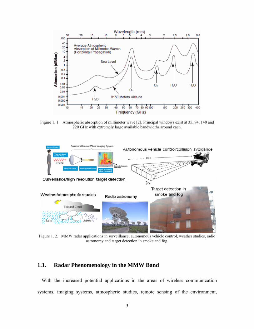
Figure 1. 1. Atmospheric absorption of millimeter wave [2]. Principal windows exist at 35, 94, 140 and 220 GHz with extremely large available bandwidths around each. .......... 3 Figure 1. 2. MMW radar applications in surveillance, autonomous vehicle control, weather studies, radio astronomy and target detection in smoke and fog. ......................... 3 Figure 1. 3. 94 GHz radiometric image of a person concealing two handguns beneath a heavy sweater [10]. ............................................................................................................ 5 Figure 1. 4. MMIC chip sizes versus cost, yield and packing density for a high-yield MESFET process using ion-implantation .. It shows as the chip size increases less chips are obtained from the wafer and hence lower yield and high cost are resulted. ................. 8 Figure 1. 5. 94-GHz FMCW radar using a horn antenna and microstrip ........................... 9 hexaferrite circulator [15]. .................................................................................................. 9 Figure 1. 6. Procedures used for target discrimination and detection. The time domain polarimetric response of the walking body undergoes processes such as Fourier transform and time-frequency analysis to derive a means for identifying human body and detecting concealed objects. ............................................................................................................. 10 Figure 1. 7. The University of Michigan W-band polarimetric radar is used for human body RCS measurement. ................................................................................................... 12 Figure 1. 8. Waveguide-based helical slot antenna. ......................................................... 13 Figure 2.1. The setup for in-vivo measurement of the skin dielectric constant. ............... 18 Figure 2.2. (a) A person wears the lycra suit equipped with reflectors. The captured positions of these reflectors from one of the cameras are shown in the right inset. (b) The captured positions of the reflectors estimate a skeleton. ................................................... 22 Figure 2.3. Facet distribution in the ear, thigh, finger and face. The non-uniform descretization involves the smaller parts have finer facets (fingers and ears) while larger parts have larger facets (thighs). ....................................................................................... 24 Figure 2.4. Area of 612,224 facets comprising a human body surface. The non-uniform
division has led to the facet sizes distribution from 5.42 in leg to
2410 in head .......... 24
Figure 2.5. Linear interpolation is performed between each two adjacent facets from each frame in order to estimate the “in-between” frames. ........................................................ 26 Figure 2.6. Dog model and facet distribution ................................................................... 27 Figure 2.7. Handgun model and facet distribution ........................................................... 27 Figure 2.8. Normalized back scattering RCS of a lossy sphere with 105 jr versus normalized frequency ak0 compared with exact solution (Figure 3.20 in [29]) . It is obvious that by increasing the normalized frequency, the PO approach tends to the exact solution. ............................................................................................................................. 31

viii
Figure 2.9. Normalized RCS of a lossy sphere with 105 jr and 2a for perpendicularly polarized incident wave compared with exact solution (Figure 3.21 in [29]). ............................................................................................................................. 32 Figure 2.10. Normalized RCS of a lossy sphere with 105 jr and 2a .................. 32 for parallel polarized incident wave compared with exact solution (Figure 3.22 in [29]).32 Figure 2.11. The interaction between two flat facets. ...................................................... 34 Figure 2.12. RCS of 900 PEC dihedral corner reflector with dimensions
6988.56988.5 at 9.4 GHz in [31] compared to IPO results. ........................................... 36 Figure 2.13. Human body is illuminated in different orientation. For each orientation the scattered field and radar cross section are calculated. ...................................................... 40 Figure 2.14. (a) First and (b) second order electric current distribution on human body when it is illuminated from the front side. The second order distribution is represented in log-scale. ........................................................................................................................... 40 Figure 2.15. (a) first and (b) second order current distribution on human head. First order currents are distributed almost everywhere which in not shadowed and have larger amplitudes in the areas which are more perpendicular to the direction of propagation. Second order currents are concentrated on concave and irregular parts. .......................... 41 Figure 2.16. Second order electric current distribution in log-scale. It is observable that current is zero in convex areas like head, and is concentrated in irregular areas like around nose, eyes, ears, and upper chin. Convex areas in face like cheeks, chin, forehead and eyebrows have also zero induced currents. ................................................................ 41 Figure 2.17. Illuminated and shadowed parts of the body for 00 incident angle. ..... 42 Figure 2.18. Human body RCS, first order results. ......................................................... 43 Figure 2.19. Co- and cross-polarized responses from the first and second iterations. .... 44 Figure 2.20. (a) thin man (b) oversize woman (c) oversize man models, front and side views. ................................................................................................................................ 45 Figure 2.21. The qualitative current distribution on the surface of the oversize woman model................................................................................................................................. 45 Figure 2.22. The IPO responses for (a) oversize man (b) oversize woman (c) thin man and (d) thin woman targets at 00 incident angle. Different amplitude level can be observed for different sizes and genders ........................................................................... 46 Figure 2.23. backscattering response of the target in the present of the ground plane includes: (a) the backscattering response of the target (b) the response of the target when the incident field is the reflected wave from the ground plane (c) the scattered field of the target is reflected by the ground plane and makes a backscattering response. ................. 47 Figure 2.24. The IPO responses for (a) oversize man (b) oversize woman (c) thin man and (d) thin woman targets at 010 incident angle. Different amplitude level can be observed for different sizes and genders. .......................................................................... 48 Figure 2.25. The IPO responses for (a) oversize man (b) oversize woman (c) thin man and (d) thin woman targets at 020 incident angle. Different amplitude level can be observed for different sizes and genders ........................................................................... 49 Figure 3.1. Moving human body is illuminated by a monostatic radar in the same direction as walking. ......................................................................................................... 54 Figure 3.3. (a) Fourier transform of scattering amplitude of human walking. (b) Fourier transform of scattering amplitude of human walking versus )2/( 00 k to give the velocities.

ix
It can be seen that it has peaks around its average velocity (v=1.8 m/s) from 1.4 to 2.1m/s. (c) the extended plot to find maximum velocity which is approximately 5.3m/s. 55 Figure 3.4 (a) Fourier transform of the scattering amplitude of each component of the walking human body versus )2/( 00 k . ............................................................................... 57 Figure 3.5. Doppler spectra of walking bodies with different sizes and genders. (a) oversize male body (b) oversize female body and (c) thin male body. ............................ 59 Figure 3.6. Doppler spectrum of a thin woman obliquely walking with respect to the radar with 450 angle. It is observable that the velocity content is lower, the maximum velocity is 3.8 (which is 5.4/ 2 )as expected). However, it is definitely not a oversize body since the energy is not highly concentrated around the average velocity. ................................. 59 Figure 3.7. Current distribution on some parts of dog’s face. .......................................... 61 Figure 3.8. (a) Doppler spectrum of scattering amplitude of a walking dog versus velocity )2/( 00 k . It can be seen that it has peaks around its average velocity (v=0.8 m/s) and the maximum and minimum velocities are2.5 m/s and 0.2 m/s (b) Doppler Spectrum of human body presented in the previous report. .............................................................. 61 Figure 3.9. (a) Polarization response of sphere and (b) torso. .......................................... 64 Figure 3.10. Backscattering response of the legs and arms during walking for different walking positions. It is lower when they are spread out (t = 0.15 s, t = 0.65 s) and higher when they are aligned with the body (t = 0.4 s, t = 0.9 s). ................................................ 67 Figure 3.11. The position of human body during walking at different time frames (approaching the radar). It is observable that around t = 0.15 s and t = 0.65 s where the legs and arms are spread out, the RCS of legs and arms are lower as shown by Figure 3.10. Similarly, around t = 0.4 s and t = 0.9 s when the legs and arms are aligned with the body, the response is higher. ............................................................................... 67 Figure 3.12. The signal is multiplied by a number of shifted Gaussian functions. .......... 69 Figure 3.13. The co-polarized response of the human body is Fourier transformed using time-frequency analysis. (a) full body (b) the limbs and (c) the torso. The signal is chopped into a number of sub-signals using a number of shifted Gaussian signals and the Fourier transformed is performed on the resulting sub-signals. The plots show different bandwidths for different frames. For the full body, while there are moments (around t = 0.4 s and t = 0.9 s) in which the velocity of the legs and arms are maximum and bandwidth is wide, there are some other times (around t = 0.15 s and t = 0.65 s) that their velocity is minimum and the bandwidth is narrow. The bandwidth of the limbs’ spectrum is narrow around t = 0.15 s and t = 0.65 s and confined around the same velocity as torso is located. At other moments, when legs and arms have higher velocities, their spectrum is wideband and spread out, while the spectrum of torso is narrow around the middle-velocity at all times. .......................................................................................................... 70 Figure 3.14. Temporal backscattering response of torso and the full body at two instances: (a) the limbs are spread out and the spectrum is narrow. (b) the limbs are aligned with the body and the spectrum is wide. The filtered response of the full body resembles that of the torso at both instances. .................................................................... 71 Figure 3.15. the gun is placed on the human waist where a handgun is actually carried. 72 Figure 3.16. Paper-mache model of upper thigh, torso and head. .................................... 74 Figure 3.17. W-band RCS measurement setup for human body. It is mounted on top of a turntable. ........................................................................................................................... 75

x
Figure 3.18. Polarimetric response of torso is measured using a 95 GHz radar (a) without and (b) with a handgun.It is observable that the presence of the firearm increases the cross-polarized response ................................................................................................... 75 Figure 3.19. (a) The qualitative current distribution on human body and (b) the Doppler spectrum of walking at 240 GHz. ..................................................................................... 76 Figure 3.20. The required antenna beamwidth to provide footprints commensurate to human body width............................................................................................................. 77 Figure 4.1. Block diagram of the Y-band FMCW radar. .................................................. 80 Figure 4.2. (a) stepped ramp and (b) stepped FMCW signals for moving targets. ........... 82 Figure 4.3. Radar range versus RCS is represented for some sample targets. Target that fall under the curve are detectable .................................................................................... 87 Figure 4.4. (a) Bulk micromachining: the microstructure is fabricated by DRIE etching of silicon substrate [61]. (b) Surface micromachining: the microstructure is fabricated using lithography of a thick ........................................................................................................ 90 SU-8 photoresist layer [62]. .............................................................................................. 90 Figure 4.5. Sidewall scalloping of DRIE process ............................................................. 90 Figure 4.6. Schemetic of 3-D silicon stacked carrier SiP [63]. Chips 1 to 4 are connected with the flip-chip method and chip 5 with wire bonding. ................................................. 92 Figure 4.7. (a) Thickness versus spin speed of SU-8 series 2100. (b) meander-line structure fabricated by spinning SU-8 2100 in two steps. The structure is gold-sputtered after developing and hard-bake. ........................................................................................ 95 Figure 5.1. The two-dimensional structure of the antenna ............................................... 97 Figure 5.2. (a) Different configuration of slots cut on the walls of a rectangular waveguide. (b) Planer meander-line waveguide slot antenna (d) unit cell of the proposed structure............................................................................................................................. 98 Figure 5.3. The current distribution on the broad wall of the rectangular waveguide. (a) For l = n
0g it is noticeable that the direction of the electric field on the slot is reversed.
(b) The reverse is compensated by adding adding a 2/0g waveguide segment. ........... 100
Figure 5.4. (a) Electric field distribution inside the waveguide for curved and diagonal cut bends. (b) Reflection coefficient from the bends. The diagonal cut bend is 450 and lb = 0.85 mm. ......................................................................................................................... 102 Figure 5.5. (a) The unit cell of the meander-line structure optimized for minimum reflection at the center frequency with 50 µm separating walls. (b) Reflection coefficient for the unit cell. It is minimized for the center frequency. (c) Reflection coefficient for nine unit cells. The constructive interference at some other frequencies causes a high reflection. (d) The unit cell of the meander-line structure with 250 µm separating walls optimized for minimum reflection at the beginning and end of the band. (e) Reflection coefficient for the unit cell. (f) Reflection coefficient for nine unit cells ....................... 103 Figure 5.6. (a) Unit cell with reflection cancelling slot and the analytical far-field pattern of the array at the beginning, center and end of the band. (b).The final proposed structure with additional slot across the broad wall of the waveguide and the analytical far-field pattern of the array at the beginning, center and end of the band. It is observable that the grating lobe is around -8 dB lower. ................................................................................ 104 Figure 5.7. (a) Normalized slot impedance versus frequency. A resonance happened at 282 GHz. (b) The total power associated with a non-resonant slot for two different widths.......................................................................................................................................... 106

xi
Figure 5.8. The slot width for each four turns so that nine different widths are used for the 36 turn waveguide. The length of the slots is 380 m. ................................................... 107 Figure 5.9. Hybrid-coupled patch array fed by the main slot ......................................... 108 Figure 5.10. (a) series-fed patch array, (b) equivalent circuit model of the series-fed patch array. ............................................................................................................................... 110 Figure 5.11. (a) equivalent circuit model of the hybrid-coupled patch array, (b) directivity of the hybrid-coupled patch array and the S-parameters of the waveguide for the center patch length of 380 um. The lengths of the center patch and connecting line to the series-fed array are optimized in such a way that the directivity is maximized and the S-parameters show resonance and (c) far-field radiation pattern of the antenna. ........... 112 Figure 5.12. Electric field distribution for air substrate at 230 GHz (a) 80 um substrate (b) 250 um substrate (c) 250 um substrate with silicon walls ......................................... 113 Figure 5.13. (a) Electric field at the boundary of two dielectric materials. The electric field distribution under a patch element excited from a very thin slot far from the patch element assisted by (b) high dielectric vertical walls (c) dielectric block. ..................... 113 Figure 5.14. (a) The proposed hybrid-coupled patch array with silicon block to enhance slot-patch coupling. (b) The electric field distribution (c) the radiation pattern at the center frequency 237.5 GHz and (d) the directivity over the frequency band. ............... 114 Figure 5.15. A developed version of hybrid-coupled patch array compatible with microfabrication. ............................................................................................................. 114 Figure 5.16. (a) The directivity and (b) return loss versus frequency of the patch array of Figure 5.15. lr = 950 µm ................................................................................................. 115 Figure 5.17. (a) The final structure (b) the radiation pattern in azimuth direction to verify the frequency scanning. .................................................................................................. 116 Figure 5.18. (a) Non-uniformity in the etched surfaces caused by DRIE. (b) Waveguide loss versus height. It is shown that by decreasing the height, loss increases. ................. 118 Figure 5.19. Two cells of the antenna structure are simulated with randomly-distributed defects with 20 µm height and 50 µm × 100 µm area (corresponding to the largest bump experimentally measured) ............................................................................................... 119 Figure 5.20. Waveguide loss (a) versus waveguide height for width = 1100 μm (b) versus waveguide width for height = 700 μm .......................................................................... 120 Figure 5.21. The dispersion diagram: propagation constant (β) versus frequency. The slope is decreased for the reduced-loss waveguide ......................................................... 120 Figure 5.22. The slot width for each four/two turns so that eight different widths are used for the 28 turn waveguide. The length of the slots is 400 m. ....................................... 121 Figure 6.2. (a) Suspended E-plane probe excitation. (b) Microfabrication of short-circuited probe for in-plane CPW is performed on two wafers: one for waveguide trench and the probe, the other for CPW line. The two wafers are bonded to form the transition.......................................................................................................................................... 126 Figure 6.3. (a) A short-circuited pin in a reduced height rectangular waveguide and its equivalent circuit. In the circuit model, Lp is the equivalent inductance and Cb is the series capacitance of the short-circuited probe [80] and Z0 is the characteristic impedance of the waveguide. (b) E-plane step discontinuity generates a shunt capacitance (Xstep ) required to achieve a resonance needed for the mode conversion and the equivalent circuit model for the proposed transition. ....................................................................... 126
xii
Figure 6.4. CBCPW to rectangular waveguide transition, top view, side view and the perspective of a back-to-back configuration which includes a transition from CBCPW to CPW, CPW to reduced-height waveguide and reduced-height waveguide to the standardWR-3 rectangular waveguide. ........................................................................... 128 Figure 6.5. (a) Equivalent circuit model for the transition. (b) Reflection coefficient of the circuit model of the back-to-back structure for the initial values of ZCBCPW=50 , ZCPW=85 , Xt = - j 140 , X = - j 110 , n = 1, Xb = - j 8 , Xp = + j 58 , Xstep = - j 1000 , lbackshort = 5 mm = g /3, l2 = 10 mm = 2g /3 , l3 = 17 mm compared to the coefficient of the full wave analysis for optimized values of S1 = 1.46 mm, W1 = 0.37 mm, S2 = 0.972 mm, W2 = 0.247 mm, WWG = 7.112 mm, hWG = 3.556 mm, h1 = 0.379 mm, h2 = 1.65 mm, t = 0.49 mm, l1 = 5.024 mm, l2 = 9.97 mm, and l3 = 16.8 mm . The waveguide dimensions are set as the standard dimensions of WR-28 Ka-band waveguides. ..................................................................................................................... 130 Figure 6.6. (a) Electric field distribution at 30GHz for a back-to-back transition with the optimized values (b) Reflection and transmission coefficients for the back-to-back transition at Ka-band. (c) transmission coefficient at the passband. ............................... 131 Figure 6.7. The bandwidth of the transition is increased to about 15% as a result of having a three-pole structure by adding one resonance, a shorting pin and a step discontinuity with h3 = 2.26 mm, l1 = 5 mm, l2 = 10 mm, l4 = 3.3 mm, l5 = 6 mm,. Additional resonances can be introduced for further enhancement. ............................... 131 Figure 6.8. A transition from a 50 ohm CPW line patterned on top of the substrate to the CBCPW line patterned on the bottom layer. The lines are connected through electroplated via holes. (b) side view. ............................................................................. 132 Figure 6.9. (a) The CBCPW trench, reduced-height waveguide and the standard waveguide are machined on a brass plate. (b) the top cover includes the lines is a substrate whose both sides are etched with CPW patterns. ............................................ 132 Figure 6.10. Simulation compared to measurement results for reflection and transmission coefficients which show a good agreement with the simulation. The observed deviations from the simulation are attributed to misalignment, especially near the pin positions and possible air gaps between the substrate and the brass unit ............................................. 134 Figure 6.11. Simulation results of a structure with misalignments (300 m translational displacement) between the top substrate and the brass unit compared to the measured results. The transmission is decreased for frequencies lower than 29 GHz and the impedance match near 31 GHz is not as good as that of the optimized ......................... 135 Figure 6.12. Transmission and reflection coefficient of the back-to-back structure (a) S1 = 210 µm, g1 = 45 µm, S2 = 140 µm, g2 = 30 µm, h1 = 46 µm, l1=330µm, l2 =450µm, t =100µm, h2 =159 µm, WWG =864 µm, hWG =432 µm l3 = 2.44 µm, showing insertion loss less than 1 dB. (b) same values except for h2 =143 µm, l3 = 5.24 µm, showing higher bandwidth and insertion loss of lower than 1.5 dB for the back-to-back structure. ....... 135 Figure 6. 13. Transmission coefficient of the transition when (a) hWG is varied ± 20 µm (~5%) showing the response of the transition is insensitive to variations in waveguide height, b) the response is shown to be more sensitive to the reduced waveguide height h2
for h > 5 µm . (c) The transmission and (d) the reflection coefficients when a gap is assigned between the top of the pin on the bottom wafer and the top wafer. The response degrades for gaps above 3 µm. ....................................................................................... 137 Figure 6. 14. The proposed configuration for integration of the multiplier and VCO .... 138
xiii
Figure 6. 15. (a) Schematic of the thru-wafer transition for chip packaging. (b) a hole is etched on the bottom wafer for the chip and for the DC line transfer. (b) The structure of the packaging after bonding and embedding the external chip. ...................................... 140 Figure 6. 16. The transition between the chip and CBCPW. It includes an intermediate step of narrow transmission line with /2 length ............................................................ 140 Figure 6. 17. The transmission coefficient of the back-to-back transition in Figure 5 (a) for different gap values. ........................................................................................................ 141 Figure 6. 18. The transmission line chip designed to test the packaging. ........................ 141 Figure 6. 19. (a) The structure of E-plane two-pole filter. (b) The equivalent circuit model.......................................................................................................................................... 143 Figure 6. 20. (a) The reflection coefficient of the filter presented in Figure 1 with t1=75 µm, l1=2.344 mm, t2=365 µm, l2= l1, t3= t1, l3= 638.6 µm. (b) The response of the same filter with various values for l= l2= l1 maintaining λ /4 difference. ................................ 143 Figure 6. 21. (a) The structure of the three-pole filter. (b) The response of the filter for with t1=117 µm, l1= 636 µm, t2=466 µm, l2=1.562 mm, t3= t1, t4= t2, l3= l1, l4= l2 ......... 144 Figure 7.1. The radar structure fabrication steps. (a) First wafer includes waveguide trench and multi-step structure of the waveguide transition (b) Second wafer includes slots and CPW line patterns with the patch substrate on the other side (c) Third wafer includes the patch arrays. The wafers are connected using wafer bonding processes. ... 146 Figure 7.2. Multi-step etching process for the First wafer. (a) Three different mask layers are deposited and patterned. (b) The wafer is etched with the last mask layer down to the desired thickness. (c) The mask layer is removed. (d) The wafer is etched with the next mask layer. (e) The mask layer is removed. (f) The wafer is etched with the final mask layer. (g) The mask layer is removed. The process can be carried on for more number of steps as long as the appropriate mask layer is chosen. ................................................... 147 Figure 7.3. (a) The schematic of the transition from grooved CPW to the CBCPW (b) Bottom substrate with top layer removed. The backwall shown in (b) should not be covered with gold (c) Top view of very short section of grooved CPW (d) the proposed structure for fabrication to avoid gold deposition on the sidewalls. ............................... 150 Figure 7.4. The grooved CPW (a) before (b) after removing the shadow walls. (c) SEM photo of the backwall (tilted 200) which verifies that the shadow walls prevented gold deposition effectively. ..................................................................................................... 150 Figure 7.5. (a) Three-step patterning the waveguide. (b) Meander-line waveguide. (c) back-to-back CBCPW to waveguide transition. (d) waveguide filter with the transition......................................................................................................................................... 151 Figure 7.6. Second wafer fabrication process. A stacked layer of LPCVD SiO2/Si3N4/SiO2 (ONO) as a membrane followed by gold is deposited. Then gold is patterned with the mask of (a) CPW and CBCPW lines. (b) the slots. (c) The wafer is flipped over and the backside is etched from the top of the areas around CBCPW and slots. ................................................................................................................................ 153 Figure 7.7. Fabricated second wafer. (a) top side- CPW/CBCPW lines (b) top side - slots......................................................................................................................................... 153 Figure 7.8. First and second wafers. (a) before gold-gold thermocompression bonding (b) after bonding ................................................................................................................... 153 Figure 7.9. (a) First wafer before bonding. (b) the meander-line slot antenna after bonding, (c) the low-loss design (d) the CBCPW/waveguide transition, (e) the

xiv
CPW/CBCPW transition, (f) calibration standards, from left to right: thru, line, open, short, offset short. ........................................................................................................... 154 Figure 7.10. (a) multi-step etching for the patch array substrate. Thin shadow walls are also formed to protect the sidewalls of the silicon block from gold-deposition. (b) gold-coating the substrate. (c) the realistic version of the structure. ....................................... 155 Figure 7.11. First and second wafers. (a) before gold-gold thermocompression bonding (b) after bonding ............................................................................................................. 155 Figure 7.12. Fabricated patch array substrate ................................................................. 156 Figure 7.13. Third wafer fabrication process. (a) photoresist, Parylene and patterned gold are deposited on a silicon wafer. (b) photoresist is dissolved by soaking the wafer in acetone and IPA. ............................................................................................................. 158 Figure 7.14. Fabricated third wafer after dissolving the photoresist release layer. ........ 159 Figure 7.15. Last step of the fabrication process. (a) The gold-bonded pair is Parylene-coated. (b) The wafers are aligned and (c) bonded. (d) The third wafer is de-bonded with a razor blade through the edges. ..................................................................................... 159 Figure 7.16. Final fabricated structure. ........................................................................... 160 Figure 7.17 Fabrication process of the transition between the chip and the CBCPW. (a) two-step pattering (b) two step etching (c) gold sputtering for the first wafer. (d) top wafer (membrane, line patterns and etching the open areas). (e) top-bottom wafers gold bonding. (f) inserting the chip inside. ............................................................................. 161 Figure 7.18. Fabrication process of a test chip (a) pattering gold on a silicon wafer (b) etching the backside of the wafer to thin down to the desired chip thickness. ............... 161 Figure 7.20. The bottom and the top wafer of the fabricated transition. It is observed that the holes on the bottom wafers are partially covered by the top wafer. ......................... 162 Figure 7.21. Yield of the radar structure with 4 inch and 6 inch wafers. It can be observed that while only two radars (including one transmitter and one receiver antennas) can be fabricated on a 4 inch wafer, eight radars (one pair of antennas) can be fabricated on a 6 inch wafer. ....................................................................................................................... 163 Figure 8.1. WR-3 (220-325 GHz) measurement setup. .................................................. 167 Figure 8.2. GGB CS-15 calibration substrate with line, thru, matched load, short and open. ................................................................................................................................ 168 Figure 8.3. The measured transmission and reflection coefficients of the back-to-back transition structure of Figure 6.4. The results are in good agreement with the simulation. The transmission coefficient is below -1.5 dB for the two series transitions and the waveguide section in between. ....................................................................................... 168 Figure 8.4. The measured (a) reflection and (b) transmission coefficient of the filter shown in Figure 6. 19 compared to the full-wave simulation. The nulls of the filter are precisely detected and the results are in good agreement with the simulation. .............. 168 Figure 8.5. The proposed setup to measure the antenna near-field. ............................... 171 Figure 8.6. (a) Straight and (b) twisted waveguide probes to measure co- and cross-polarized field components. ............................................................................................ 171 Figure 8.7. The XY stage used to move the near-field waveguide probe. ...................... 171 Figure 8.8. Measurement setup for the near-field measurement of the E-plane horn. ... 172 (c) .................................................................................................................................... 173
xv
Figure 8.9. (a) S21 magnitude versus the scanned area at f = 237.5 GHz. (b) The time-domain and the gated response with Kaiser filter for the received signal at x = 0. (c) The normalized far-field radiation pattern verifies 100 HPBW. ............................................ 173 Figure 8.10. The setup proposed for the antenna measurement. The antenna is excited through the GSG probes and the radiated power is measured with a waveguide probe. The waveguide probe is connected to the frequency extender through a waveguide bend and its position is controlled by the XY stage. ............................................................... 175 Figure 8.11. The waveguide probe moving on top of the slot openings. ........................ 175 Figure 8.12. Radiation pattern of the GSG probe. .......................................................... 176 Figure 8.13. The structure simulated to calculate the power radiated from the slots ..... 176 Figure 8.14. The reflection loss of the waveguide slot array. ......................................... 176 Figure 8.15. (a) The S21 intensity measured over the slot openings. .............................. 177 Figure 8.16. (a) S21 intensity measured over the slot openings of the reduced-loss design. (b) S21 intensity over the cells shown in part (a). ........................................................... 178 Figure 8.17. The time domain response at two different spots on top of the slots. ........ 179 Figure 8.18. (a) Far-field radiation pattern at different frequencies, beamwidth = 8.50. 180 Figure 8.19. Etched area of the bottom wafer (a) before and (b) after bonding. The SEM photo in the inset shows around 5~10 µm roughness. .................................................... 180 Figure 8.20. Gold quality on the bottom wafer after bonding (a) without and (b) with a diffusion barrier layer. .................................................................................................... 181 Figure 8.21. (a) S21 intensity measured over the slot openings of the reduced-loss design with the diffusion barrier layer. (b) S21 intensity over the cells shown in part (a). ........ 182 Figure 8.22. Far-field radiation pattern of the reduced-loss design with the diffusion barrier layer at different frequencies, beamwidth = 3.50. ............................................... 182 Figure 9.1. The effect of heavy clothings with wrinkles on the radar backscatter. ........ 188 Figure 9.2. Etch non-uniformity of long structure caused by DRIE ............................... 190 Figure 9.3. (a) v-polarized and (b) proposed feeding technique for h-polarized antennas for the same slot. ............................................................................................................. 191

xvi
LIST OF TABLES
Table I . The dielectric constant of human skin predicted by analytical models and measurement. The results show that the value of the reflection coefficient undergoes only maximum of 6% deviation. By taking the ratio of cross- to co-polarized response, the effect of the dielectric constant is even less important. .................................................... 18 Table II. The average values of the co- and cross-polarized responses of different human bodies. The higher amplitude for the larger size targets is noticeable. ............................. 46 Table III. The average values of the co- and cross-polarized responses of different human bodies for 010 and 020 ........................................................................................... 50 Table IV. The RCS of the torso and legs and arms and also their ratio at four sample positions where the legs and arms either aligned with torso or are spread out. ................ 66 Table V. cross- to co-polarized response of the walking human body at two instances, where the limbs are aligned with the body and where they are spread out. The response is increased when the handgun is present. ............................................................................ 73 Table VI. Radar specifications. ......................................................................................... 80 Table VII. Microfabrication processes used for 2.5D stacked structures ......................... 92 Table VIII. The scanning angle of the antenna for different wall thicknesses and lengths between elements. ........................................................................................................... 100 Table IX. The scan angle and directivity versus frequency. ........................................... 117 Table X. The estimated cost and time of microfabrication for different processes on a 6 inch wafer. The estimated total cost is 428 $/ 6 inch wafer which results in 428 $ / 8= 53$ for each radar including a pair of transmitter and receiver antenna. .............................. 163 Table XI. The scan angle versus frequency for the waveguide slot array. ..................... 180 Table XII. The scan angle versus frequency for the waveguide slot array (reduced-loss design with the diffusion barrier layer) ........................................................................... 183

xvii
LIST OF ABBREVIATIONS
MMW Millimeter-wave SMMW Submillimeter-wave PO/IPO Physical Optics/Iterative Physical Optics RCS Radar Cross Section DRIE Deep Reactive Ion Etching GO Geometrical Optics FMCW Frequency Modulate Continuous Wave CBCPW Cavity-Backed CoPlanar Waveguide ONO Oxide Nitride Oxide

xviii
ABSTRACT
A Millimeter-Wave Radar Microfabrication Technique and Its
Application in Detection of Concealed Objects
by
Mehrnoosh Vahidpour
Chair: Kamal Sarabandi
Millimeter-wave (MMW) radars are envisioned for a number of safety and security
applications such as collision-avoidance, navigation and standoff target detection in all
weather conditions. This work focuses on two MMW radar applications: (1)
phenomenology of radar backscatter from the human body for the purpose of
identification and detection of concealed objects on the body (2) microfabrication of
advanced MMW radar to achieve compact and low-cost systems for autonomous
navigation.
In MMW band, the wavelength (1 mm ~ 1 cm) is long enough to allow signal
penetration through cluttered atmosphere and clothing with little attenuation and short
enough to allow for fabrication of small-size radar systems. Hence, this frequency band is

xix
well suited for the design of small sensors capable of obstacle detection and navigation in
heavily cluttered environment and detecting hidden objects carried by individuals. For
this purpose, a novel non-imaging approach is developed for distinction of walking
human body and concealed carried object using polarimetric backscatter Doppler
spectrum. This approach does not need radiometric calibration of the radar and
preparation of the subject for radar interrogation. It is shown that a coherent polarimetric
radar at W-band (95 GHz) or higher frequencies can be used for standoff detection of
concealed carried objects.
Motivated by these results, the thesis also includes an investigation on developing a
technology for compact MMW radar systems. A micromachined, high-resolution,
compact and low-power imaging MMW radar operating at 240 GHz intended for obstacle
detection in complex environment is introduced. A frequency scanning antenna array
micromachined from three layers of stacked silicon wafers is designed to provide 20
beamwidth in azimuth and 80 in elevation with azimuthal beam scanning range of 250.
The frequency beam scanning is enabled by a meander rectangular waveguide with a slot
array on its broad wall to feed linear microstrip patch antennas microfabricated on a
suspended Parylene membrane. This technique offers high fabrication precision; provide
easy fabrication and integration with active devices. The performances of the passive
components of the radar system are verified using a WR-3 S-parameter and a near-field
measurement systems.
1
Chapter I
1. Introduction
The millimeter wave (MMW) spectrum is a range of electromagnetic band between 30
GHz and 300 GHz corresponding to wavelengths form 10mm to 1mm, between
microwave and THz/optical region. The current interest in MMW band arises from the
understanding of the limitations with the adjacent frequency bands [1]. In the microwave
region, atmospheric loss is significantly low and excellent penetration through many
obstacles such as walls, clothing, vegetation, fog and dust can be realized. In addition, the
technology for radars operating at microwave band has matured significantly. This
includes high-power transmitters, low power electronics, data collection and storage as
well as signal processing techniques for noise reduction and enhanced target detection.
However, for applications where very high resolution is required, utilization of radars
operating at low frequencies is impractical due to the required large aperture and very
wide fractional bandwidth. Moreover, the microwave band is small, overcrowded and
protected for wireless telecommunication networks, long-range military, weather and
traffic control radars. Alternatively, optical range of spectrum requires small apertures
and provides high resolution and the phenomenology of wave interaction is well
understood and interpreted. Nevertheless, the physical dimension of the objects under
detection are large compared to the wavelength which brings up the necessity of either
using computers with significant amount of memory and fast processors for analysis or
applying asymptotic methods of analysis. Also, lack of technology in developing

2
coherent sources, sensors and detectors in optical range makes many potential
applications unfeasible. Furthermore, due to the high atmospheric attenuation, most
obstacles such as dust and smoke are no longer transparent at this range.
The main advantages of the MMW range are:
Short wavelength: the component sizes are reduced compared to those in the microwave
band. This makes them suitable for mobile platforms such as aircrafts, helicopters, cars or
even small robotic platforms. It is also possible to achieve lower beamwidth (l
) which
results in better resolution.
Wide bandwidth: Investigating atmospheric absorption for horizontal propagation over
400 GHz of bandwidth including the MMW band (Figure 1. 1) represents that the
principal windows exist at 35, 94, 140 and 220 GHz with extremely large available
bandwidths around each. This has a number of advantages:
High data rate for communication systems,
High resistance to jamming since wide bandwidth is available,
Very high range resolution for tracking and target detection,
Increased recognition capability of slowly moving target due to the high Doppler
frequency
Low sensitivity to environmental characteristics Atmospheric absorption and
attenuation due to inclement weather condition such as fog, dust or smoke are much
lower compared to optical and IR frequencies [3].
3
Figure 1. 1. Atmospheric absorption of millimeter wave [2]. Principal windows exist at 35, 94, 140 and 220 GHz with extremely large available bandwidths around each.
Figure 1. 2. MMW radar applications in surveillance, autonomous vehicle control, weather studies, radio
astronomy and target detection in smoke and fog.
1.1. Radar Phenomenology in the MMW Band
With the increased potential applications in the areas of wireless communication
systems, imaging systems, atmospheric studies, remote sensing of the environment,

4
surveillance, navigation, autonomous vehicle control, radio astronomy, high resolution
target detection, perimeter security, etc (Figure 1. 2), the MMW part of electromagnetics
spectrum has received extensive attention over the past two decades. One of the main
applications of MMW radars is in the area of surveillance, perimeter security and
detection of pedestrians and hidden objects carried by individuals in heavy-cluttered
environment. Detection and identification of human beings in highly scattering radar
scenes such as urban and indoor environments is rather challenging. Traditional detection
systems include metal detectors and X-ray systems. The latter has hazardous health
effects for human, while the former detects metal by measuring magnetic field generated
by eddy current and can only be used in situ and is incapable of distinguishing harmless
small personal objects [4]. More elaborate systems employ imaging techniques to identify
the targets [5] - [9]. MMW imagers offer high resolution for a compact system while
providing see-through-clothing and day-and-night operation capabilities. Furthermore,
unlike X-rays, MMW radiation is non-ionizing, leading to minimal health risks. These
make the MMW band ideally suited for surveillance of individuals for many applications
ranging from identification of the human body itself to detection of concealed weapons.
Both active (reflecting) and passive (radiometric) MMW imaging systems have been
investigated for these purposes. Passive systems are based on electromagnetic emission
and apparent temperature variations of human body and concealed objects. Such imagers
operate on the principle that a metallic weapon will reflect the temperature of the ambient
surroundings at a different degree compared to the human body. This contrast is then
detected by the radiometer and weapons can be recognized if the radiometer has
sufficient spatial resolution [10]. Figure 1. 3 shows an image obtained from such a system

5
that clearly shows two handguns hidden beneath a person’s sweater. On the other hand,
active MMW radars illuminate the targets and build the images based on the reflected
signal. Some of these systems use combined MMW-IR or MMW-Optical sensors in order
to take advantage of both MMW penetration through clothing and very high resolution of
the IR/optical range [11]. Focal plane arrays, pupil plane array and phased arrays have
been extensively used in the detection of explosives concealed beneath the clothing [11],
[12]. These arrays are large for moving platforms and costly since they use complex
circuitry.
(a) (b) Figure 1. 3. 94 GHz radiometric image of a person concealing two handguns beneath a heavy sweater
[10].
Identification of moving targets –such as walking or jogging human or animals - can be
accomplished from the analysis of their backscatter Doppler spectrum. Due to the
wideband spectrum compared to microwave frequencies, more details of human motion
can be detected. This feature, in addition to the high-resolution capability of MMW
radars, makes such radars more attractive for identification of walking bodies. The
proposed methods for detection of human body and carried objects [13] rely on the

6
absolute value of the response which requires radiometric calibration of the radar and the
knowledge of RCS of the human body at all incident angles. This of course is not
practical due to the fact that the RCS of different human subjects are very different. There
is a very large RCS variability as a function of aspect angle, and if the subject is partially
illuminated or if it is not in the far-field region of radar system, its RCS becomes a
function of radar range and radar beam. To circumvent these difficulties to some extent
the application of polarimetric radars is proposed for which narrow beams with footprints
commensurate to human body can be generated. Also using radar polarimetry,
radiometric calibration will not be required. However, at lower microwave frequencies,
the human body can depolarize the backscatter signal considerably and therefore cross-
polarized signature cannot effectively be used. In addition, for narrow beamwidths, very
large antennas are required. At high MMW frequencies, the amount of co-polarized
backscatter response is dominant for smooth targets and cross-polarized response
represents the level of roughness and asymmetry of the target. Uneven and asymmetric
targets generate greater cross-polarized response. The geometries of common concealed
objects carried by individuals are highly irregular and, once placed near human body, can
indeed increase the level of cross-polarized backscatter observed by MMW radars.
Therefore, at higher MMW frequencies, a significant increase in the cross-polarized
response can be an indication of an external irregular object and can be used for
detection. For detection of external irregular objects, the overall radar backscatter
response of human body is decomposed into components associated with the body parts
using time-frequency analysis. Isolating the torso response and noting that the presence
of irregular objects on or around the torso increase cross- to co-polarized backscatter

7
ratio, it is shown that a coherent polarimetric radar at W-band or higher frequencies can
be used for standoff detection of concealed objects.
A part of this thesis is focused on utilizing the backscatter Doppler spectrum at MMW
frequencies to identify walking human bodies from other stationary and moving objects
and using radar polarimetry in conjunction with time-frequency analysis for detecting
concealed objects on a walking human subject.
1.2. Radar Technology in the MMW band
The first generations of MMW radars were large in size mainly due to the utilization of
tube oscillators and amplifiers and bulky antennas. Moreover, beam scanning was
performed mechanically which required high mechanical accelerations in order to
achieve high speed scanning or tracking. Recent advances in RFIC and MMIC
technologies have made the fabrication of light-weight and less costly VCO and amplifier
chips more feasible. Figure 1. 4 represents the MMIC chip sizes versus cost, yield and
packing density for a high-yield MESFET process using ion-implantation. It shows that
for smaller chips, cost decreases while the yield and density increases. This provides a
major incentive to employ MMIC for MMW radar fabrication. Also, understanding the
advantages of frequency modulated continuous wave (FMCW) radars which are fully
compatible with these technologies, and the need for smaller, lighter, cheaper and low
power systems, have focused the attentions on the realization of the on-chip fully
integrated FMCW systems. At 24, 77, and 94 GHz, on-chip systems have been fabricated
for automotive applications such as autonomous vehicle control and sensors for industrial
robots and for range detection and target identification [13] - [19]. These designs are

8
using waveguides or MMIC consisting of mechanically or electrically tunable voltage-
controlled oscillators (VCO), couplers, low noise amplifier, high electron-mobility
(HEMT) transistors, mixers, circulators (for single transmit-receive antenna) etc. The
solid state designs use a wide variety of different substrates from GaAs [15] to LTCC
[18], [20] and silicon [21]. Recently, silicon germanium has been widely used at
frequencies above 100 GHz to increase operating speed, reduce electronic noise, lower
power consumption, support higher levels of integration, and, thus, enables the design of
more functional components on a chip. However, in most of these systems, the antenna is
a separate module which is connected to the MMIC via a transition. This makes the
structure bulky and large while the transition adds additional loss to the system, whereas
antenna integration enhances system loss, weight and compactness. However, most of the
integrated systems employ simple antennas with limited performance such as patches
with fixed and wide beams.
Figure 1. 4. MMIC chip sizes versus cost, yield and packing density for a high-yield MESFET process using ion-implantation. It shows as the chip size increases less chips are obtained from the wafer and hence
lower yield and high cost are resulted.
0 20 40 60 80 100 chip size (mm2)
9
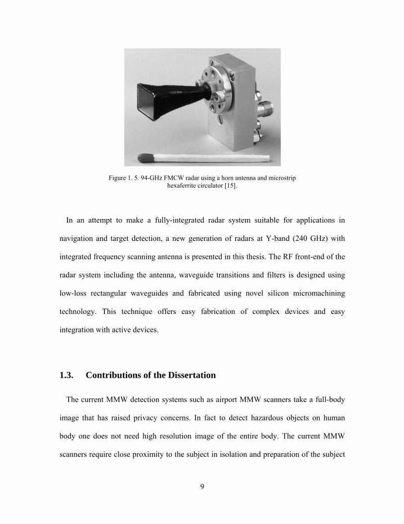
Figure 1. 5. 94-GHz FMCW radar using a horn antenna and microstrip hexaferrite circulator [15].
In an attempt to make a fully-integrated radar system suitable for applications in
navigation and target detection, a new generation of radars at Y-band (240 GHz) with
integrated frequency scanning antenna is presented in this thesis. The RF front-end of the
radar system including the antenna, waveguide transitions and filters is designed using
low-loss rectangular waveguides and fabricated using novel silicon micromachining
technology. This technique offers easy fabrication of complex devices and easy
integration with active devices.
1.3. Contributions of the Dissertation
The current MMW detection systems such as airport MMW scanners take a full-body
image that has raised privacy concerns. In fact to detect hazardous objects on human
body one does not need high resolution image of the entire body. The current MMW
scanners require close proximity to the subject in isolation and preparation of the subject
10
by requiring removal of all coats and jackets. The method proposed in this dissertation
does not image the body and does not require the individual to be isolated from its
surrounding, so the radar does not need to be radiometrically calibrated. It relies only on
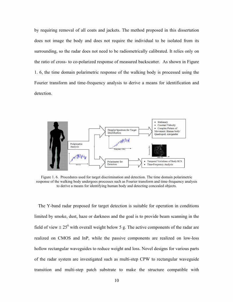
the ratio of cross- to co-polarized response of measured backscatter. As shown in Figure
1. 6, the time domain polarimetric response of the walking body is processed using the
Fourier transform and time-frequency analysis to derive a means for identification and
detection.
Figure 1. 6. Procedures used for target discrimination and detection. The time domain polarimetric response of the walking body undergoes processes such as Fourier transform and time-frequency analysis
to derive a means for identifying human body and detecting concealed objects.
The Y-band radar proposed for target detection is suitable for operation in conditions
limited by smoke, dust, haze or darkness and the goal is to provide beam scanning in the
field of view 250 with overall weight below 5 g. The active components of the radar are
realized on CMOS and InP, while the passive components are realized on low-loss
hollow rectangular waveguides to reduce weight and loss. Novel designs for various parts
of the radar system are investigated such as multi-step CPW to rectangular waveguide
transition and multi-step patch substrate to make the structure compatible with

11
microfabrication techniques. The designed structures have features aligned with Cartesian
coordinates, do not incorporate dielectric materials and can be easily integrated. Novel
microfabrication processes are used for the fabrication of passive components which
include multi-step DRIE process, gold thermocompression bonding, controlled
metallization on the sidewalls and realization of very large membranes using Parylene
transfer method. The performance of the system is verified using assembled WR-3
measurement setups for S-parameter and near-field measurements.
1.3.1. Overview of the Dissertation
This dissertation discusses the application of MMW radars in identification of walking
human body and detection of concealed carried objects on human body in complex
highly cluttered scene, and microfabrication of advanced MMW radars to achieve
compact and low-cost systems for autonomous navigation.
Chapter II describes an efficient method for the radar backscatter analysis of human
bodies in the high MMW band - Physical Optics (PO) and Iterative Physical Optics
(IPO). Realistic body models including human bodies with different sizes and genders,
dog and handgun are generated using laser scan and reference photographs of real targets.
The body motion models are generated using a motion capture system. The simulated
Radar Cross-Sections (RCS) of these targets at W-band are then calculated and the
feasibility of target identification is discussed.
Chapter III discusses the radar backscatter analysis of walking bodies at W-band
(Figure 1. 7). The Doppler spectra of human body and a dog models are derived from the

12
calculated backscatter signal in the time domain. The polarimetric responses of the
walking bodies are then studied and the feasibility of detecting body-attached irregular
objects by decomposing the overall backscatter response from different body parts is
investigated. Based on the results, a novel method on the detection of external carried
objects is developed and discussed. Experimental results of human body RCS
measurement with/without carrying a handgun with the University of Michigan W-band
radar system are presented to verify the carried object detection algorithm.
Figure 1. 7. The University of Michigan W-band polarimetric radar is used for human body RCS
measurement.
Human Doppler analysis at Y-band is performed using the same method. Y-band
compared to W-band is underutilized and the available bandwidth is much higher and Y-
band radars require technological advances to be well-suited for navigation and obstacle
detection. These motivate the development of a Y-band radar which can be later
enhanced for polarimetric applications and concealed target detection.
Chapter IV introduces a new generation of MMW radars at Y- band. The radar is low-
profile and low-cost with high range resolution for navigation and obstacle detection. It is
ultra-light weight and compact compared to the state of the art systems with components
13
fabricated on MMIC and assembled eventually on the antenna substrate. The radar
antenna is a frequency scanning array with 250 steering capability with narrow (20)
beamwidth. The radar components and specifications as well as and the antenna
characteristics are presented and discussed. The motivations behind suggesting the
antenna structure and the radar assembly with low-cost micromachining techniques are
presented.
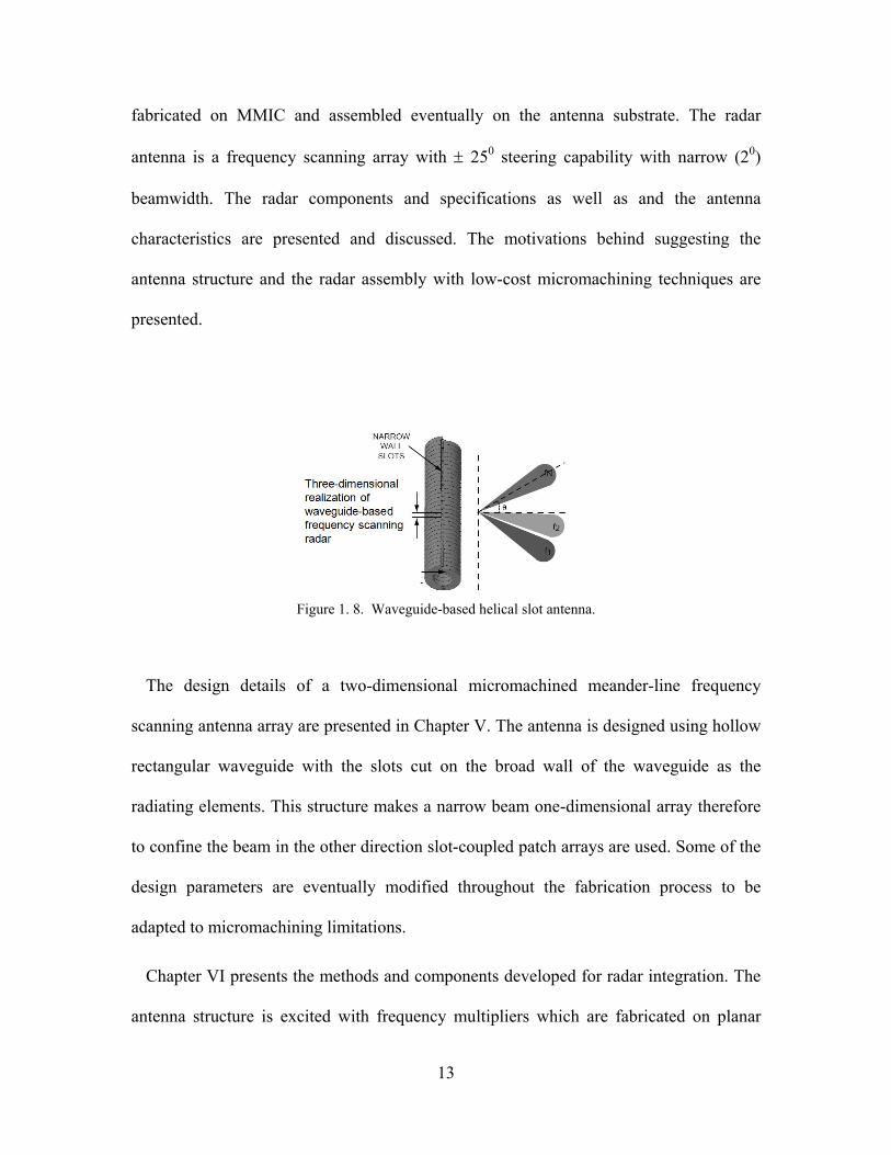
Figure 1. 8. Waveguide-based helical slot antenna.
The design details of a two-dimensional micromachined meander-line frequency
scanning antenna array are presented in Chapter V. The antenna is designed using hollow
rectangular waveguide with the slots cut on the broad wall of the waveguide as the
radiating elements. This structure makes a narrow beam one-dimensional array therefore
to confine the beam in the other direction slot-coupled patch arrays are used. Some of the
design parameters are eventually modified throughout the fabrication process to be
adapted to micromachining limitations.
Chapter VI presents the methods and components developed for radar integration. The
antenna structure is excited with frequency multipliers which are fabricated on planar

14
transmission lines. Therefore, waveguide transitions to such transmission lines are
required. In addition, a new method is developed to integrate the external chips of
frequency multipliers and VCO with the antenna substrate. Waveguide bandpass filters
are also designed to be incorporated with the system mainly in order to remove the
unwanted components of the signal received by the antenna. The components and
integration techniques are developed in a manner to be compatible with micromachining
processes used to fabricate the antenna substrate.
Chapter VII discusses the details of microfabrication processes of the structure. The
antenna is fabricated with a Deep Reactive Ion Etching (DRIE) method using silicon as
the structural material. The process is performed on three silicon wafers each of which
include a part of the antenna and other passive devices which are bonded together at the
final step. Various microfabrication procedures such as silicon DRIE, gold sputtering,
gold evaporation, multi-step mask deposition, silicon-oxide deposition, low-stress
silicon-oxide/silicon nitride deposition, XeF2 silicon etching, gold thermocompression
bonding, topside and backside wafer alignment, polymer deposition and polymer bonding
are employed and optimized for the fabrication of the radar components.
Chapter VIII presents the measurement setup for the Y-band system and discusses the
on-wafer measurement process, calibration and antenna pattern measurement approach.
The measurement results are presented and discussed.
This thesis concludes with a summary of its contributions and future work on this
research topic in Chapter IX.

15
Chapter II
2. Electromagnetics Scattering Analysis of Human Body
The MMW region of electromagnetic spectrum offers certain unique features that can
be utilized in detection and identification of individuals from their surroundings. In this
region, the wavelength is short enough to allow fabrication of compact radars and achieve
higher resolution. Yet, at the same time, the wavelength is long enough to allow signal
penetration through non-conductive objects, clothing, smoke and fog with little or no
attenuation. These make the MMW band ideally suited for surveillance of individuals for
many applications ranging from the identification of the human body itself to the
detection of concealed weapons ([8], [9]). Specifically, higher MMW bands can be used
for radar backscatter analysis of human body since:
Human motion has a unique pattern which is captured more easily at higher
MMW band due to the higher recognition capability of Doppler at higher frequencies.
The response of human-like targets is mostly co-polarized at high MMW
frequencies. This is due to the fact that the radii of the curvatures of the body are much
larger than the wavelength. This feature can be utilized to detect external carried objects
by human body when a high cross-polarized response is received.
Smaller size antennas can provide narrow beams with footprints commensurate to
human body.
The penetration depth is much smaller than the wavelength. Therefore, the target
can be considered as a surface and there is no need to model the internal organs.

16
At W-band and higher MMW frequencies, dimensions of a typical human body are
very large compared to the wavelength and therefore methods based on full-wave
analysis are not practical for present computers. However, the radii of curvature on
human body are much larger than the wavelength which makes it a suitable candidate for
high frequency methods. In addition, as will be shown later, the human skin at MMW
frequencies is very lossy. Thus a homogenous dielectric can be assumed and the
equivalent induced electric and magnetic currents on the surface of the body can be
approximated using the physical optics (PO) model. The PO model for human body
should perform well as the penetration depth is small and as a result the multipath within
the dielectric body can be ignored. However, the PO approach does not account for the
interactions between different body parts and, therefore, does not guarantee the accuracy
of the cross-polarized response. To account for the interactions and to enhance the
accuracy, the iterative physical optics (IPO) method is employed and utilized for radar
backscatter analysis of human body to calculate the total scattered field and the scattering
matrix of the human target.
In this chapter, first the characteristics of human body models such as the surface body
models and skin dielectric constant are discussed. The PO/IPO methods along with
Geometrical Optics (GO) method are introduced and their formulations are presented.
Since the IPO method is very time/memory intensive, some simplifying methods are
presented to reduce analysis time. Then the results of radar backscatter analysis with
these methods for human bodies with different sizes/genders are presented and the
feasibility of human body identification based on the radar backscatter response is
discussed.

17
2.1. Characteristics of the Human Body Models
2.1.1. Dielectric constant of skin
In order to simulate the radar response of the human body at W-band and higher
frequencies, it can be modeled as homogeneous dielectric material since the skin depth of
the targets is less than 1 mm. The electric permittivity of the skin at MMW frequencies
obtained from the Debye equation is:
jjj s
rrr 1)()()(
(1)
Where m.S 4.1 and , mF1085.8 s,109.6 ,0.42 ,0.4 120
12 s
These parameters were obtained experimentally and have been shown to provide an
adequate representation of the complex dielectric constant of human skin at microwave
frequencies [22]. In [23] the complex permittivity of ex-vivo sample of human skin fixed
in formaldehyde was measured over the band of 60 to 100 GHz using a quasi-optical
method which shows deviation from the predicted Debye model. Table I lists a number of
models which present electric permittivity of the human skin. Considering the fact that
human skin is very lossy at MMW frequencies, a set of in-vivo measurements have been
conducted using open-ended rectangular waveguide aperture radiating into skin which is
considered as a homogeneous dielectric sample with relative complex dielectric constant.
In this set of measurements, a calibrated open-ended WR-10 waveguide being tightly in
contact with a finger’s skin was used as shown in Figure 2.1 and the S11 is measured. By
analyzing this structure with Ansoft HFSS and tuning the value of the dielectric constant
to fit the measured S11, we can find the relative permittivity and loss tangent of the skin.

18
It is noticed that even for a specific person, depending on the location, the skin dielectric
constant can change considerably. This variability depends on the moisture, cleanness,
skin thickness, etc. The table shows some sample measurements showing this variability
and a comparison with the proposed models. The Fresnel reflection coefficient at normal
incidence for each value of dielectric constant is also presented. This comparison is made
to indicate that the surface reflectivity is not much affected by the small variations by
different models and measured values. Besides, by taking the ratio of cross- to co-
polarized response - which is needed in the detection algorithm as will be shown later -
this effect is even less important.
Figure 2.1. The setup for in-vivo measurement of the skin dielectric constant.
Relative permittivity
(95 GHz)
Loss tangent (95 GHz)
Reflection coefficient at normal incidence
(magnitude) Debye model [22] 6.11 1.42 0.4333
Four term Cole-Cole expression (Walters [24])
5.8 1.3 0.4218
Four term Cole-Cole expression (Gabriel [25])
7.51 1.156 0.4691
Measurement with open-ended
waveguide
Sample 1 5.7 1.12 0.4163
Sample 2 6 1.05 0.4254
Table I . The dielectric constant of human skin predicted by analytical models and measurement. The results show that the value of the reflection coefficient undergoes only maximum of 6% deviation. By
taking the ratio of cross- to co-polarized response, the effect of the dielectric constant is even less important.

19
The University of Michigan polarimetric W-band radar system works at 95 GHz and at
this frequency, skin dielectric constant (Debye model) is 7127.81154.6 j . For such a
medium the penetration depth is:
0763.0)Im(2
11
0
r
(2)
Since the penetration depth is much smaller and radii of human body’s curvature is
much larger than the wavelength, and also since the skin is lossy, we can make use of PO
method and model the body as a homogeneous dielectric material by equivalent surface
currents. Thus a homogenous dielectric can be assumed and the equivalent induced
electric and magnetic currents on the surface of the body can be approximated using the
PO model.
It is worth mentioning here that most clothings appear mainly transparent at MMW
frequencies. This fact is used nowadays in most prevalent MMW imaging systems
installed at airports. Even for thicker clothing where attenuation can be slightly higher
than the usual, the clothing alone does not increase the ratio of cross- to co-polarized ratio
which is the metric we use for detection of relatively large concealed objects.
2.1.2. Surface Human Body Models
In order to be able to analyze the radar backscatter of human body with the PO method,
surface human models are required. The creation of a humanoid character suitable for use
with these experiments went through several stages which consisted of: modeling,
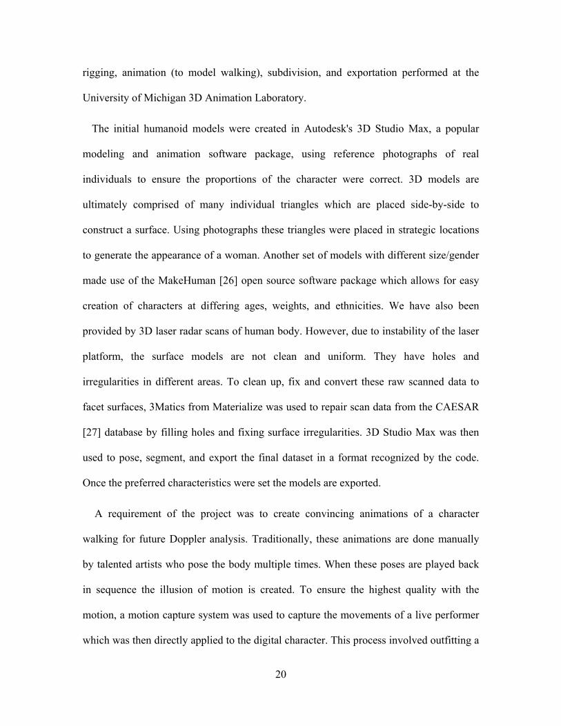
20
rigging, animation (to model walking), subdivision, and exportation performed at the
University of Michigan 3D Animation Laboratory.
The initial humanoid models were created in Autodesk's 3D Studio Max, a popular
modeling and animation software package, using reference photographs of real
individuals to ensure the proportions of the character were correct. 3D models are
ultimately comprised of many individual triangles which are placed side-by-side to
construct a surface. Using photographs these triangles were placed in strategic locations
to generate the appearance of a woman. Another set of models with different size/gender
made use of the MakeHuman [26] open source software package which allows for easy
creation of characters at differing ages, weights, and ethnicities. We have also been
provided by 3D laser radar scans of human body. However, due to instability of the laser
platform, the surface models are not clean and uniform. They have holes and
irregularities in different areas. To clean up, fix and convert these raw scanned data to
facet surfaces, 3Matics from Materialize was used to repair scan data from the CAESAR
[27] database by filling holes and fixing surface irregularities. 3D Studio Max was then
used to pose, segment, and export the final dataset in a format recognized by the code.
Once the preferred characteristics were set the models are exported.
A requirement of the project was to create convincing animations of a character
walking for future Doppler analysis. Traditionally, these animations are done manually
by talented artists who pose the body multiple times. When these poses are played back
in sequence the illusion of motion is created. To ensure the highest quality with the
motion, a motion capture system was used to capture the movements of a live performer
which was then directly applied to the digital character. This process involved outfitting a

21
performer with special reflective markers, which is a lycra suit equipped with small, ball-
shaped reflectors. Each reflector consists of special retroflective tape from 3M wrapped
in a ball and strategically placed on the subject as shown in Figure 2.2 (a). A set of eight
cameras then track these reflectors as the subject moves about with each camera having
its own "view" of the captured volume. A computer communicates with each camera and
cross references what the cameras "see" to calculate the position of each marker in space.
Connections are made between these markers to build up a skeleton which determines the
proportions of the character. Then a digital model is created based on those proportions to
generate human body shape. The surfaces were created by hand using the photographs for
measurements. Figure 2.2 (b) represents the reflector points captured by one camera
which build a skeleton. Through this process one can animate the skeleton (a few simple
objects) and have the complex humanoid mesh deform according to the position and
orientation of the individual bones. This greatly simplifies the animation process as one
does not need to animate each individual vertex or point in the mesh and allows for easier
use of motion capture data.
The process of binding a mesh to the skeletal structure (also known as skinning) can be
a lengthy task as one needs to assign each vertex/point of the mesh to the appropriate
bone. In areas such as the shoulder or hips one specific points need to receive influence
from multiple bones to create a smooth deformed surface, which can add to the
processing time. Once the mesh has been bound to the underlying skeleton it is free to
animate. For this project, the motion capture data was applied to the character and
trimmed to a looping walk cycle that was 30 frames (~1 second) in length.
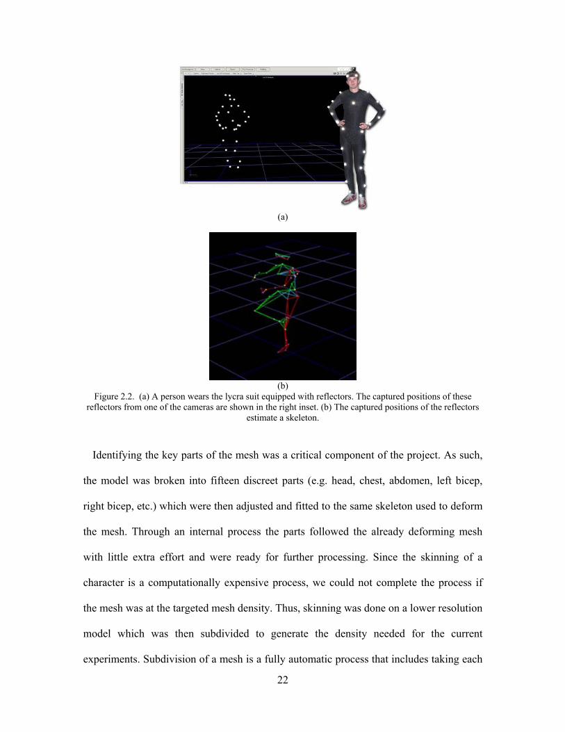
22
(a)
(b)
Figure 2.2. (a) A person wears the lycra suit equipped with reflectors. The captured positions of these reflectors from one of the cameras are shown in the right inset. (b) The captured positions of the reflectors
estimate a skeleton.
Identifying the key parts of the mesh was a critical component of the project. As such,
the model was broken into fifteen discreet parts (e.g. head, chest, abdomen, left bicep,
right bicep, etc.) which were then adjusted and fitted to the same skeleton used to deform
the mesh. Through an internal process the parts followed the already deforming mesh
with little extra effort and were ready for further processing. Since the skinning of a
character is a computationally expensive process, we could not complete the process if
the mesh was at the targeted mesh density. Thus, skinning was done on a lower resolution
model which was then subdivided to generate the density needed for the current
experiments. Subdivision of a mesh is a fully automatic process that includes taking each

23
existing polygon (often limited to a quadrilateral) and dividing it into four parts. Once the
individual meshes representing the various sections of the body were animated and set to
the proper resolution, they were exported to the STL (stereolithography) format using a
custom script written for 3D Studio Max. The developed script analyzes the existing
scene and exports the mesh at each time step. Due to the complexity of the dataset, each
time step often took several minutes to be written to file. This file contains the
coordinates of flat facets with non-uniform sizes on the surface of human body, along
with their normal vectors [28]. The total number of triangular facets varies depending on
the model size and posture. The facets sizes are non-uniform, large in areas like arms and
legs, middle-sized in torso, and very small in hands, toes and some parts in face as shown
in Figure 2.3. Figure 2.4 represents the area of the facets in different body parts. It is
noticeable that meshing is adaptive and large facets belong to legs, arms and torso areas.
However, the number of the exported frames is not enough for monitoring the motion
at 95 GHz. Since the model walks around 1.8 m in one second on average, the distance
between frames is approximately around 6 cm, which is much larger than the wavelength
at 95 GHz. To calculate the number of frames required for the analysis, we must have
information about the velocity of the fastest component of the body. Suppose we do not
have any moving particle faster than vmax, the Doppler shift we end up with for this
particle is: tvk max02 . To have the minimum required samples of this function (Nyquist
rate), tvk max02 must be sampled each times. Hence we have
)4/(/4222 max0max0max02max01max0 vttvtvktvktvk
and the number of samples is:
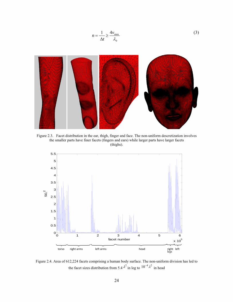
24
0
max41
v
tn
(3)
Figure 2.3. Facet distribution in the ear, thigh, finger and face. The non-uniform descretization involves the smaller parts have finer facets (fingers and ears) while larger parts have larger facets
(thighs).
Figure 2.4. Area of 612,224 facets comprising a human body surface. The non-uniform division has led to
the facet sizes distribution from 5.42 in leg to
2410 in head
0 1 2 3 4 5 6
x 105
0
0.5
1
1.5
2
2.5
3
3.5
4
4.5
5
5.5
facet number
S/
2
torso right arms left arms head right left legs

25
Assuming vmax=5.5m, 7000n . It will be proven later that the maximum velocity of
any body part cannot exceed this number for our present human models. However, the
process of exporting data for this large number of frames is extremely time- and memory-
intensive. To resolve this issue the idea of “tweening” is used. It is the creation of
intermediate frames between two key points. Here the estimation of the information of
the required frames in between each two frames is performed by linear interpolation. For
the human body example, if we can extract 250 frames between every two frames, a total
number of 7500 frames is achieved which satisfies the Nyquist rate. The linear
interpolation procedure is illustrated in Figure 2.5 for two identical facets from two
adjacent sequences. The coordinates of the vertices and the normal vectors for 249 facets
in between is derived as
25001
0
AAiAAi
(4)
where iiii zyxA . Having determined the coordinates of all the facets of the 7500
frames, the backscattering response for each facet can be calculated using PO method and
the total electric field of a frame by superposing all the responses:
N
n
nss EE
1
where N
is the number of facets. The scattering parameters for frames can then make a sequence
as follows
750021 ... xxxxxxxx SSSS (5)

26
Figure 2.5. Linear interpolation is performed between each two adjacent facets from each frame in order to
estimate the “in-between” frames.
where ixxS is the backscattering response of the xx component, of the ith frame. This
sequence of the backscattering response generates a time domain signal which is Fourier
transformed to derive the Doppler spectrum for each polarization.
In addition to analyzing different bodies with different size/genders, a walking
quadruped model is also analyzed. In this analysis, a real dog (a short-haired Labrador)
along with its anatomy information is used as a reference to model and animate the
walking dog. The same procedure is performed and thirty frames per second in one step
of walking are modeled. Then the surface of the body in each frame is discretized to
triangular facets. Figure 2.6 shows the dog model and facet discretization. The same idea
of tweening used here as well to compute all the required frames. The only difference is
that since dog has smaller range of movements, a smaller number of frames is required to
model the walking at W-band (95 GHz).
To analyze the polarimetric radar backscatter response of the individual who carries a
handgun, a generic model of a handgun is also needed. For this purpose, 3D laser radar
scans of a real handgun are taken. The data undergoes a similar process as above to
render the surface model for a handgun as well. The model is shown in Figure 2.7.

27
Figure 2.6. Dog model and facet distribution
Figure 2.7. Handgun model and facet distribution
2.2. Physical Optics / Iterative Physical Optics Approach
2.2.1. Physical Optics
For the models consisting of flat facets, the current distribution and scattered field for
each facet are modeled first. When an incident field impinges upon a flat surface, we can
determine the induced currents on the surface from tangential components of fields:
)(ˆ)(ˆ)(
)(ˆ)(ˆ)(
rEnrEnrM
rHnrHnrJ
sis
sis
(6)
Where, sJ
and sM
are induced surface currents, ii EH
, are magnetic and electric
incident fields, while rkjki
rkjki
ii eErEeHrH
.ˆ
0.ˆ
000 )(,)( and ss EH
, are magnetic and
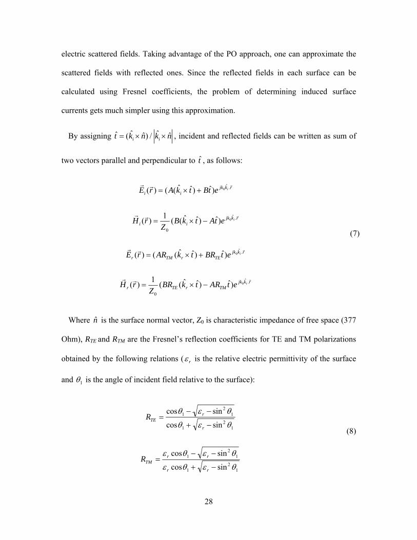
28
electric scattered fields. Taking advantage of the PO approach, one can approximate the
scattered fields with reflected ones. Since the reflected fields in each surface can be
calculated using Fresnel coefficients, the problem of determining induced surface
currents gets much simpler using this approximation.
By assigning ˆ ˆˆ ˆ ˆ( ) /i it k n k n , incident and reflected fields can be written as sum of
two vectors parallel and perpendicular to t , as follows:
rkjkii
ietBtkArE
.ˆ0)ˆ)ˆˆ(()(
rkjkii
ietAtkBZ
rH
.ˆ
0
0)ˆ)ˆˆ((1
)(
rkjkTErTMr
ietBRtkARrE
.ˆ0)ˆ)ˆˆ(()(
rkjkTMrTEr
ietARtkBRZ
rH
.ˆ
0
0)ˆ)ˆˆ((1
)(
(7)
Where n is the surface normal vector, Z0 is characteristic impedance of free space (377
Ohm), RTE and RTM are the Fresnel’s reflection coefficients for TE and TM polarizations
obtained by the following relations ( r is the relative electric permittivity of the surface
and 1 is the angle of incident field relative to the surface):
12
1
12
1
sincos
sincos
r
rTER
12
1
12
1
sincos
sincos
rr
rrTMR
(8)

29
Substituting the fields (7) into (6) and using vector algebra to simplify, we get to the
following relation for surface currents [29]:
)ˆˆ)(1)(ˆ(ˆ)1)(ˆ)(ˆ()(
)ˆˆ)(1)(ˆ(ˆ)1)(ˆ)(ˆ(1
)(
000).ˆ(
000
).ˆ(
0
0
tnRtEtRkntHZerM
tnRtHtRkntEZ
erJ
TETMirkjk
s
TMTEirkjk
s
i
i
(9)
Utilizing these equivalent currents, we calculate the electric field in the far field using
the free-space dyadic Green’s function as follows:
S
rkjksssss
rjk
s dserMkrJZkkIr
ejkrE s ')'(ˆ)'()ˆˆ(
4)( '.ˆ
00 0
0
(10)
where, sk is the direction of observation.
This method is applicable also in simulating lossy complex targets whose radii of
curvature are much larger than a wavelength. In this case one can approximate the
surface of complex targets with a number of flat surfaces. The incident field can induce
currents on flat surfaces calculated from (9). Therefore, superposing all scattered fields
due to the induced currents on flat surfaces yields the scattered field of the complex target
N
nntotal HH
1
N
nntotal EE
1
(11)
When the total scattered field of a complex target is calculated, the scattering amplitude
matrix (S) can be determined as:

30
i
rkjk
s ESr
erE
i
0
ˆ
0
0
)( , where
vv
hv
vh
hh
vi
hi
ivs
hs
s S
S
S
SS
E
EE
E
EE ,,
vi
rkjkvs
vvhi
rkjkvs
vhvi
rkjkhs
hvhi
rkjkhs
hh E
erES
E
erES
E
erES
E
erES
iiii ˆ
0
ˆ
0
ˆ
0
ˆ
00000
,,,
(12)
Where, 0r is the distance form target to observation point. The RCS ( ) of the target is
also calculated as:
2
0
2
02
0
)(
)(
rE
rEr
i
s
(13)
2.2.2. Geometrical Optics (Shadowing Effect)
When the uniform plane wave is incident on a complex target, the areas with normal
vectors in the same direction as the wavevector are shadowed. No surface currents are
induced on the shadowed facets. To eliminate shadowed facets, Geometrical Optics (GO)
approximation is used by applying the criterion 0ˆˆ ikn . This holds for the lit areas,
where n and ik are normal vector of the facet and wave vector of incident field. We
model the lit facets with equivalent surface currents using (9), and then calculate the far
electric field from (10) and scattering amplitude (12) or RCS (13).

31
Model Verification
Based on the aforementioned method, a PO code is generated to calculate the scattering
amplitude of a lossy dielectric sphere since its analytical calculation is available to
compare with our model. We are provided with a model of sphere with radius of a = 1 m
which consists of 11840 equal-sized triangular facets. For the given value of dielectric
constant ( 105 jr [29]), penetration depth is 07.0)Im(2
11
0
r
, thus the
sphere is sufficiently lossy and it is reasonable to model the target with the equivalent
surface currents. After locating the lit facets using 0ˆˆ ikn , we model them with
equivalent surface currents using (9), and then calculate the far electric field from (10)
and scattering amplitude (12) or RCS (13).
Figure 2.8. Normalized back scattering RCS of a lossy sphere with 105 jr versus normalized
frequency ak0 compared with exact solution (Figure 3.20 in [29]) . It is obvious that by increasing the
normalized frequency, the PO approach tends to the exact solution.
0 2 4 6 8 10 12-30
-25
-20
-15
-10
-5
0
k0a
/
a2
Backscattering
our model exact solution

32
Figure 2.9. Normalized RCS of a lossy sphere with 105 jr and 2a for perpendicularly polarized
incident wave compared with exact solution (Figure 3.21 in [29]).
Figure 2.10. Normalized RCS of a lossy sphere with 105 jr and 2a
for parallel polarized incident wave compared with exact solution (Figure 3.22 in [29]).
0 20 40 60 80 100 120 140 160 180-20
-15
-10
-5
0
5
10
15
20
25
Scattering Angle
/
a2
Parallel Polarization
our results exact solution
0 20 40 60 80 100 120 140 160 180-10
-5
0
5
10
15
20
25
Scattering Angle
/
a2
Perpendicular Polarization
our model exact solution

33
Figure 2.8 to Figure 2.10 show the RCS for different angles of observation and
different frequencies. The results are compared with the exact solution presented in [29]
and show a very good agreement.
2.2.3. Iterative Physical Optics
The PO approach does not account for the interactions between different body parts
and, therefore, does not guarantee the accuracy of the cross-polarized response. To
account for the interactions and enhance the accuracy, the iterative physical optics (IPO)
method is employed and utilized for human body analysis to calculate the total scattered
field and the scattering matrix of the human target.
Since our objects are modeled by a number of flat surfaces, it is rational to explain the
IPO method considering two flat surfaces as shown in Figure 2.11. To account for the
interaction between two flat surfaces, first we calculate the first order currents using Eq.
(6). These currents reradiate and hence induce second order currents on each other.
Hence, each surface has two sources of induced currents: from incident field and from
other facets reradiating. Consider calculating the interaction of surface 1 with surface 2.
The fields induced on surface 2 due to first order currents on surface 1 is calculated as
[30]:
S
first
S
firstfirstfirstond dgrMZjk
dsgrJrMrJrH 0100
0111sec
1,2 )'(1
)'())'(),'(,(
S
first
S
firstfirstfirstond dsgrJYjk
dsgrMrMrJrE 0100
0111sec
1,2 )'(1
)'())'(),'(,(
(14)

34
Where g0 is the free space Green’s function: r
eg
rjk
4
0
0 , Z0 and Y0 are the free space
impedance and admittance and rr , are positions of surface 2 and 1, respectively as
shown in Figure 2.11.
Therefore, the induced second order currents on surface 2 are calculated from the
tangential component of second order fields:
),,(ˆ)(
),,(ˆ)(
11
sec
1,2
11
secsec
2
2
1,2
firstfirstondfirst
firstfirstondond
MJrEnrM
MJrHnrJ
(15)
And the total induced current in the second order scheme is written as:
N
n
ondsn
firsts
totals
N
n
ondsn
firsts
totals
rMrMrM
rJrJrJ
1
sec
1
sec
)()()(
)()()(
(16)
Figure 2.11. The interaction between two flat facets.
r
)(),( 11 rMrJ firstfirst
r
)(),( 22 rMrJ firstfirst
1
2

35
The induced fields in one facet are calculated by superposing all the interactions as:
N
mn
ond
nm
ond
totalm HH,1
sec
,
sec
,
N
mn
ond
nm
ond
totalm EE,1
sec
,
sec
,
(17)
Where ond
n
ond
n EH secsec ,
are the fields on facet m due to currents on facet n which are
presented for prototype facets 1 and 2 in Eq (14) and N is the number of facets.
The iterative procedure is continued until the total currents converge. It is shown that
due to free space losses during interaction, higher order field components are trivial and
currents converge very soon, especially for our object of interest, human body, in which
the component sizes are much larger than a wavelength.
Model Verification
In order to verify the above IPO scheme a 900 dihedral corner reflector is analyzed and
the results are compared with those of [31]. The structure consists of two square PEC
surfaces perpendicular to each other. The simulation is done at 9.4 GHz and the results of
the second order PO are used to calculate the RCS for the dihedral corner reflector which
is shown in Figure 2.12. The results show good agreement with that of UTD presented in
[31].

36
Figure 2.12. RCS of 900 PEC dihedral corner reflector with dimensions 6988.56988.5 at 9.4 GHz in
[31] compared to IPO results.
2.2.4. Human Body Analysis
The number of facets on the surface of human bodies range from 700,000 to 1,300,00
for different human body models in order to well accommodate the curvatures of the
bodies. According to Eq (17), if N is the number of operation for each facet, calculating
all the interactions is in the order of N2 while for the first order PO we had one operation
for each facet and calculation was in the order of N. This number of operations for higher
order PO increases the amount of processing time drastically. Basically, if the time
needed for each facet’s interaction to be completed is 5 seconds on average – which is the
limit for the current machine (quad-core AMD CPU 1.25 GHz, 8 GB RAM) – each
simulation for any given orientation of incident field will take 75 days for 1,300,00
facets. This huge work load makes us revise the approach and take advantage of some
features in human body to make the IPO analysis achievable.
Surface 1 450
Surface 2
[2]

37
2.2.4.a. Simplifications for the IPO Analysis
Impedance Boundary Condition (IBC)
The lossy nature of human skin introduces a relationship between induced electric and
magnetic fields on the surface:
HnZE s
ˆ (18)
Which is called impedance boundary condition (IBC). In this formula, Zs is the surface
impedance of the skin and is given by:
j
jZs
in which the parameters are those
of the body skin.
As mentioned, calculating Eqs (14) along with (17) is very time consuming. Eq. (18)
which relates electric and magnetic fields on the surface helps us eliminate one of the Eqs
(14). We can calculate E field from (14) and find H field simply using (18) or vice versa.
This halves the amount of computations we initially needed to perform.
The Distance of Interaction
As the field components attenuate by a factor of rk0/1 in free space and the wavelength
is much smaller than our object sizes, in many cases the fields radiating from a facet
vanish even before they reach another facet to begin interacting when they are far from
each other. Therefore, those interactions which undergo more than -40dB loss during
propagating in free space can be ignored. This criterion yields the maximum distance in
with interaction can happen as follows:

38
000 /10001.0)/1(40)/1log(20 krrkrk (19)
Which gives cmr 5 at 95GHz. This means in 5cm, the field is attenuated around -
40dB and is almost trivial; hence if there is a facet in the vicinity above this distance, the
interaction is almost zero. This results in eliminating the interaction among facets which
are farther than 5cm from each other
Far- Field Calculation
Eqs. (14) are exact formulations to calculate electric and magnetic fields from currents.
Depending on the distance of surfaces compared to wavelength they radiate either in their
far- or near- field zones. In case they are far enough, we can use the approximate far-field
formula instead of using the exact formula:
S
rkjkfirsts
first
ss
rjkfirstfirstfirst
dserMkrJZ
kkIr
ejkrMrJrE
s ')'(ˆ)'(
)ˆˆ(4
))'(),'(,(
'.ˆ
110
0112
0
0
(20)
The criterion for the far-field region of a flat surface is given by /2 2D , where D is
the maximum length of the surface. The facets’ sizes in our model are mostly smaller
than 2/ and very few facets are longer than 2/ . These facets are located in areas like
thigh and torso. As we know these areas are convex and do not generate second order
response in the surrounding areas and are too far from other areas to have any affect. So
if we consider 2/ as the largest facet size, the far-field criterion will be 2/ . The
upper limit of 2 is hence considered which is around 6mm and considering the size of
human body and distances between components, we conclude that most parts are within

39
the far-field region of each other which again simplifies the calculation by letting us use
far-field approximation instead of Eqs. (14).
Domination of Response in Specular Direction
As it is proved [32], in the specular direction, the coherent component of the scattered
field is dominant. This gives rise to criterion for dominant facets as: 1)ˆˆ(ˆ si kkn ,
where, n is facet’s normal vector and, ik , and sk are the direction of incident (from
another facet) and observation. Therefore, only facets which fall in this criterion
depending on the direction of incident field are considered for analysis.
Using all the above simplifications, the radar backscatter response of a human body (a
thin female model) was calculated. The RCS around the body was calculated by
illuminating the object by a uniform plane wave at different orientations and finding the
scattered field for each angle as shown in Figure 2.13. Figure 2.14 represents the
qualitative first and second order current distribution on human body for illumination
from the front side ( 900 in Figure 2.13). As expected there are no induced currents in
the back part of the body and near the shadow region the surface currents diminish
gently. In the second order current distribution in Figure 2.14 (b), all the dark blue parts
have zero second order currents, i.e. convex areas like thighs and torso. By investigating
the current distribution on the head presented in Figure 2.15, it is observable that second
order currents have peaks in some specific areas like lips and around eyes, and almost
zero current everywhere else

40
Figure 2.13. Human body is illuminated in different orientation. For each orientation the scattered field and
radar cross section are calculated.
side view front view
(a) (b) Figure 2.14. (a) First and (b) second order electric current distribution on human body when it is
illuminated from the front side. The second order distribution is represented in log-scale.
To have a better understanding of the second order current distribution, we presented it
in logarithmic scale in Figure 2.16. These figures show that in convex areas like the top
of the head no current is induced which is expected, but in all irregular areas like around
nose, eyes, lips and ears they are nontrivial.
y
x
y
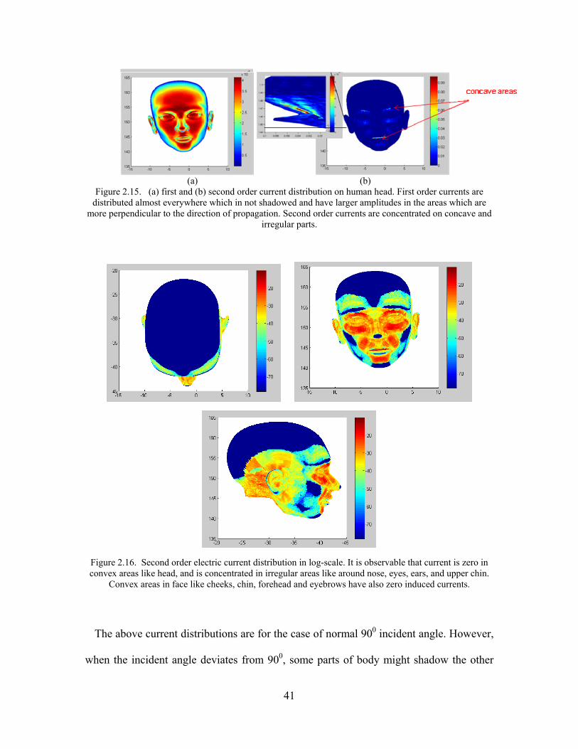
41
(a) (b)
Figure 2.15. (a) first and (b) second order current distribution on human head. First order currents are distributed almost everywhere which in not shadowed and have larger amplitudes in the areas which are
more perpendicular to the direction of propagation. Second order currents are concentrated on concave and irregular parts.
Figure 2.16. Second order electric current distribution in log-scale. It is observable that current is zero in convex areas like head, and is concentrated in irregular areas like around nose, eyes, ears, and upper chin.
Convex areas in face like cheeks, chin, forehead and eyebrows have also zero induced currents.
The above current distributions are for the case of normal 900 incident angle. However,
when the incident angle deviates from 900, some parts of body might shadow the other

42
parts. For example when 00, the right arm shadows the torso and part of the thigh, the
torso shadows the left arm, and the right leg shadows the left leg. These shadowed parts
are not simply covered by GO method, since that method deals with shadowed part which
does not see incident field originally not because they are hidden by other body parts. To
find these shadowed parts, first we need to find out the order of the body components
with respect to the direction of illumination. All the body components are partially
shadowed, hence we need to find the projection of each part on the other considering a
specific orientation of the incident wave. Figure 2.17 represents the lit areas of the body
for 00 incident angle. As it is shown, the right arm and the head are completely lit
(except for their back parts in which the shadowed areas are found using GO method. The
right-hand shape hole is observed in torso and in a part of the right leg shows these parts
are shadowed by the right hand. The left leg and arm are mostly covered so that only
some parts of fingers are shown. Exactly opposite of this happens when illumination
angle is 1800.
Figure 2.17. Illuminated and shadowed parts of the body for 00 incident angle.
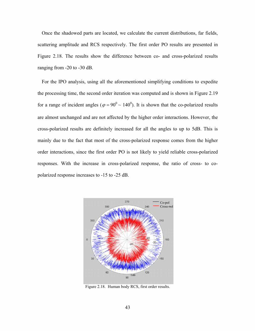
43
Once the shadowed parts are located, we calculate the current distributions, far fields,
scattering amplitude and RCS respectively. The first order PO results are presented in
Figure 2.18. The results show the difference between co- and cross-polarized results
ranging from -20 to -30 dB.
For the IPO analysis, using all the aforementioned simplifying conditions to expedite
the processing time, the second order iteration was computed and is shown in Figure 2.19
for a range of incident angles ( 900 ~ 1400). It is shown that the co-polarized results
are almost unchanged and are not affected by the higher order interactions. However, the
cross-polarized results are definitely increased for all the angles to up to 5dB. This is
mainly due to the fact that most of the cross-polarized response comes from the higher
order interactions, since the first order PO is not likely to yield reliable cross-polarized
responses. With the increase in cross-polarized response, the ratio of cross- to co-
polarized response increases to -15 to -25 dB.
Figure 2.18. Human body RCS, first order results.
Co-pol Cross-pol

44
90 95 100 105 110 115 120 125 130 135 140-70
-60
-50
-40
-30
-20
-10
0
(deg)
co-pol response
1st+2nd order1st order
90 95 100 105 110 115 120 125 130 135 140
-90
-80
-70
-60
-50
-40
-30
(deg)
cross-pol response
1st+2nd order1st order
(a) (b)
Figure 2.19. Co- and cross-polarized responses from the first and second iterations.
2.2.5. Identification of Human Bodies with Different Sizes / Genders
In addition to the thin female model, three other human models with different
sizes/genders as shown in Figure 2.20 are analyzed. The sizes of models are around the
normal human body’s for the average oversize and thin women and men.
Figure 2.21 shows the current distribution on the surface of the oversize female body
when the plane wave illumination is in the normal incident angle from the front side. The
distribution is qualitatively similar to that of the thin body. The IPO simulation results for
all four models are presented in Figure 2.22. It is noticeable that for larger targets
(oversize man and woman), the level of the response is higher. Table II represents the
average value of the responses over the circumference. Male targets have around 1~2 dB
higher co-polarized responses compared to the female targets of the same size. For each
gender, the responses of the oversize and thin samples have around 3~4 dB amplitude
difference.
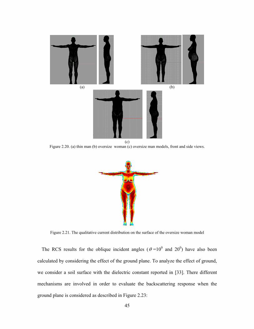
45
(a) (b)
(c)
Figure 2.20. (a) thin man (b) oversize woman (c) oversize man models, front and side views.
Figure 2.21. The qualitative current distribution on the surface of the oversize woman model
The RCS results for the oblique incident angles ( =100 and 200) have also been
calculated by considering the effect of the ground plane. To analyze the effect of ground,
we consider a soil surface with the dielectric constant reported in [33]. There different
mechanisms are involved in order to evaluate the backscattering response when the
ground plane is considered as described in Figure 2.23:

46
-60 dB
-20 dB
0 dB
20 dB
30
210
60
240
90
270
120
300
150
330
180 0
Fat Man
co-pol
cross-pol
-60dB
0 dB
20 dB
30
210
60
240
90
270
120
300
150
330
180 0
Fat Woman
co-pol
cross-pol
(a) (b)
-60 dB
0 dB
20 dB
30
210
60
240
90
270
120
300
150
330
180 0
Thin Man
co-pol
cross-pol
-60 dB
0 dB
20 dB
30
210
60
240
90
270
120
300
150
330
180 0
Thin Woman
co-pol
cross-pol
(c) (d)
Figure 2.22. The IPO responses for (a) oversize man (b) oversize woman (c) thin man and (d) thin woman
targets at 00 incident angle. Different amplitude level can be observed for different sizes and genders
Oversize man Oversize woman Thin man Thin woman
Co-polarized response (dB)
-1.6708 -3.6867 -5.0897 -6.3874
Cross-polarized response (dB)
-21.4106 -22.5764 -22.8746 -25.2444
Table II. The average values of the co- and cross-polarized responses of different human bodies. The higher
amplitude for the larger size targets is noticeable.

47
(a) (b) (c) Figure 2.23. backscattering response of the target in the present of the ground plane includes: (a) the
backscattering response of the target (b) the response of the target when the incident field is the reflected wave from the ground plane (c) the scattered field of the target is reflected by the ground plane and makes a
backscattering response.
the backscattering response of the target itself as calculated in the previous cases
the response of the target when the incident field is the reflected wave from the
ground plane
when the scattered field of the target is reflected by the ground plane.
The simulation results for oblique incident angles considering the effect of the ground
plane are presented in Figure 2.24 and Figure 2.25. In these cases, the level of the cross-
polarized response increases, while the same difference in the level of the amplitude of
the co- and cross-polarized responses for different genders and sizes are noticeable as
represented by the averages in Table III.
scatterer
ground
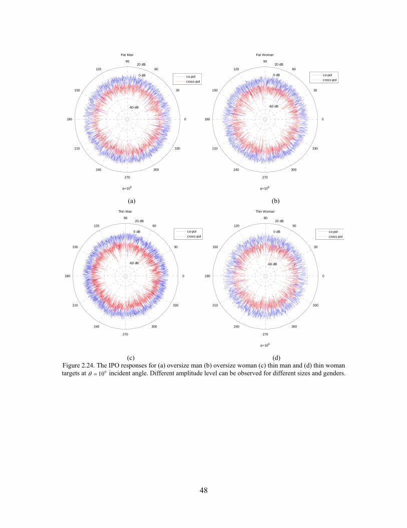
48
-60 dB
0 dB
20 dB
30
210
60
240
90
270
120
300
150
330
180 0
Fat Man
=100
co-pol
cross-pol
-60 dB
0 dB
20 dB
30
210
60
240
90
270
120
300
150
330
180 0
Fat Woman
=100
co-pol
cross-pol
(a) (b)
-60 dB
0 dB
20 dB
30
210
60
240
90
270
120
300
150
330
180 0
Thin Man
co-pol
cross-pol
-60 dB
0 dB
20 dB
30
210
60
240
90
270
120
300
150
330
180 0
Thin Woman
=100
co-pol
cross-pol
(c) (d)
Figure 2.24. The IPO responses for (a) oversize man (b) oversize woman (c) thin man and (d) thin woman targets at 010 incident angle. Different amplitude level can be observed for different sizes and genders.

49
-60 dB
0 dB
20 dB
30
210
60
240
90
270
120
300
150
330
180 0
Fat Man
=200
co-pol
cross-pol
-60
0 dB
20 dB
30
210
60
240
90
270
120
300
150
330
180 0
Fat Woman
=200
co-pol
cross-pol
(a) (b)
-60 dB
0 dB
20 dB
30
210
60
240
90
270
120
300
150
330
180 0
Thin Man
=200
-60 dB
0 dB
20 dB
30
210
60
240
90
270
120
300
150
330
180 0
Thin Woman
=200
co-pol
cross-pol
(c) (d)
Figure 2.25. The IPO responses for (a) oversize man (b) oversize woman (c) thin man and (d) thin woman targets at 020 incident angle. Different amplitude level can be observed for different sizes and genders

50
Oversize man Oversize woman Thin man Thin woman
Co-polarized
response (dB) 010
-1.3710 -3.3538 -4.5742 -5.9942
Cross-polarized
response (dB) 010
-15.5885 -17.9967 -16.4556 -16.9262
Co-polarized
response (dB) 020
-2.4570 -4.4897 -5.7288 -5.9926
Co-polarized
response (dB) 020
-15.0269 -16.9910 -15.8153 -16.9188
Table III. The average values of the co- and cross-polarized responses of different human bodies for 010 and 020
2.3. Conclusion
In this chapter, the radar backscatter analysis of human bodies at W-band was
presented. First the characteristics of human body models and the feasibility of using
PO/IPO method for human body analysis were investigated. The formulation of PO/IPO
and GO approach and a simplified formulation of IPO approach for human body analysis
were presented and discussed. The radar backscatter responses for different human bodies
with different sizes/genders were calculated and the feasibility of identifying size/gender
was discussed. It was shown that the larger targets (oversize man and woman) have
higher level of RCS response and the male targets have around 1~2 dB higher co-
polarized responses compared to the female targets of the same size.
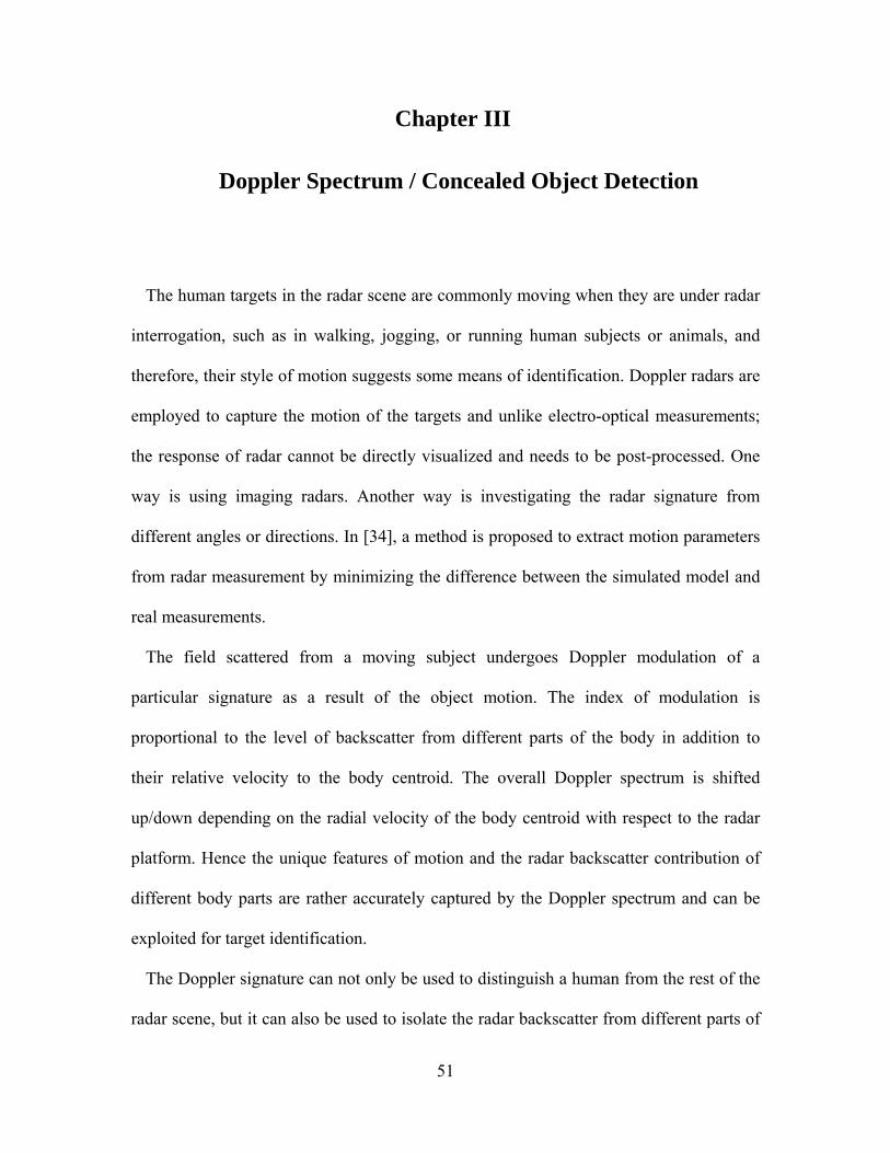
51
Chapter III
3. Doppler Spectrum / Concealed Object Detection
The human targets in the radar scene are commonly moving when they are under radar
interrogation, such as in walking, jogging, or running human subjects or animals, and
therefore, their style of motion suggests some means of identification. Doppler radars are
employed to capture the motion of the targets and unlike electro-optical measurements;
the response of radar cannot be directly visualized and needs to be post-processed. One
way is using imaging radars. Another way is investigating the radar signature from
different angles or directions. In [34], a method is proposed to extract motion parameters
from radar measurement by minimizing the difference between the simulated model and
real measurements.
The field scattered from a moving subject undergoes Doppler modulation of a
particular signature as a result of the object motion. The index of modulation is
proportional to the level of backscatter from different parts of the body in addition to
their relative velocity to the body centroid. The overall Doppler spectrum is shifted
up/down depending on the radial velocity of the body centroid with respect to the radar
platform. Hence the unique features of motion and the radar backscatter contribution of
different body parts are rather accurately captured by the Doppler spectrum and can be
exploited for target identification.
The Doppler signature can not only be used to distinguish a human from the rest of the
radar scene, but it can also be used to isolate the radar backscatter from different parts of

52
the body. Feature extraction of body movements and human gait recognition based on
Doppler radar has been investigated at lower microwave bands [13], [35]- [38]
qualitatively where the human body is modeled by a simple uniform dielectric volume or
unsophisticated models of homogeneous cylindrical and spherical objects. In [38], the
features were extracted using the time-frequency transform of the response measured by a
24 GHz Doppler radar. The possibility of discriminating between human gait and those of
other objects based on step rate and mean velocity was investigated as well.
The feasibility of detection of concealed carried objects by human body has also been
investigated with different techniques. Traditional detection systems include metal
detectors and X-ray systems. The latter has hazardous health effects when used on
humans, while the former can only be used in situ for detecting metallic objects. More
elaborate systems employ imaging techniques to identify the target and detect
contraband. These systems have been very effective, but have a number of shortcomings,
such as requiring close proximity to the subject, slow processing, violating the privacy of
individuals, and giving low-quality blurred images in a heavily cluttered environment. In
[13], detection was investigated at low microwave frequencies and slight decrease in the
amplitude of the radar return is used to detect the presence of a rifle against a human
body. However, for such techniques to be successful the response of the human must be
isolated from its surrounding, the radar needs to be radiometrically calibrated, and the
RCS of the human subject at the proper aspect angle and posture without the rifle must be
known. Considering the fact that the number of conditions one may encounter (different
body and object sizes and shapes) is enormous, algorithms that rely on quantitative RCS
values cannot be very reliable. To circumvent these difficulties to some extent the

53
application of polarimetric radars is proposed for which narrow beams with footprints
commensurate to the human body can be generated. Also using radar polarimetry,
radiometric calibration will not be required. However, at lower microwave frequencies,
the human body can depolarize the backscatter signal considerably and therefore the
cross-polarized signature cannot effectively be used. In addition, for narrow beamwidths,
very large antennas are required. At high MMW frequencies, the amount of co-polarized
backscatter response is dominant for smooth targets and cross-polarized response
represents the level of smoothness and symmetry of the target. Uneven and asymmetric
targets generate greater cross-polarized response. The geometries of common concealed
objects carried by individuals are highly irregular and, once placed near human body, can
indeed increase the level of cross-polarized backscatter observed by MMW radars.
Therefore, at higher MMW frequencies, a significant increase in the cross-polarized
response can be an indication of an external irregular object and can be used for
detection.
In this chapter, the radar backscatter responses of walking human bodies as a function
of time at W-band are calculated. The Doppler spectra of the bodies are obtained by
performing a Fourier transform of the backscatter response and the feasibility of
identifying different body sizes/genders and walking dog based on the characteristics of
the Doppler spectra are investigated. Then a radar backscatter decomposition algorithm is
presented to isolate the response of torso in order to be able to measure the cross-
polarized response of the torso. It is verified that the higher cross- to co-polarized
response of torso is an indication of the presence of irregular external object. This is also
experimentally verified by measuring the RCS of the human torso at the W-band. The

54
chapter concludes by presenting the radar backscatter analysis of the walking body at Y-
band.
3.1. Radar Backscatter Analysis of a Walking Human Body
In order to simulate the radar response of the targets in motion, detailed realistic
models are developed by the University of Michigan 3D Animation Laboratory as
described before and shown in Figure 3.1. To calculate the scattering amplitude of this
model we first select lit facets using GO. Then, the lit facets are modeled by equivalent
surface currents using (9) knowing facets’ coordinates, normal vectors, and also sizes.
Once the surface current distribution for all 7500 frames are calculated, far electric field
can be computed from (10) and scattering amplitude from (12).
Figure 3.1. Moving human body is illuminated by a monostatic radar in the same direction as walking.
incident field
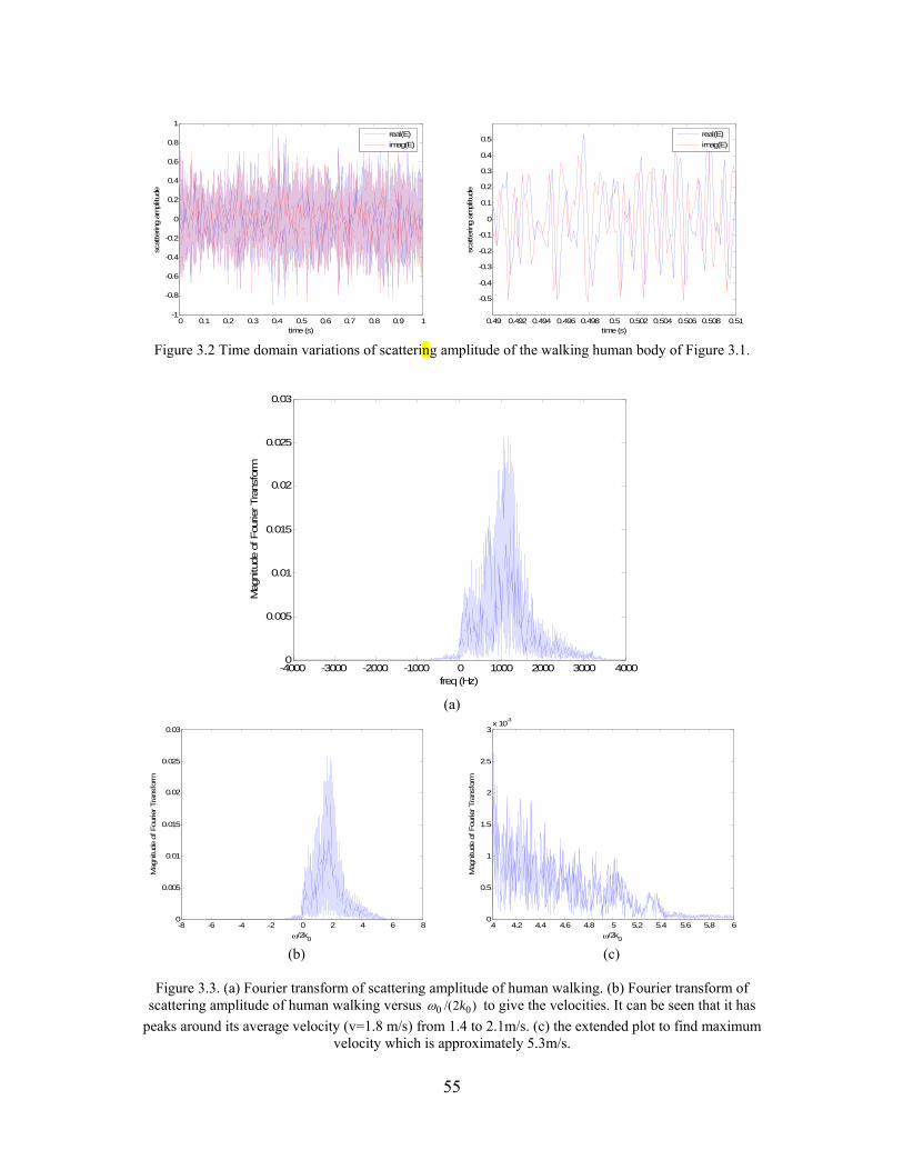
55
0 0.1 0.2 0.3 0.4 0.5 0.6 0.7 0.8 0.9 1-1
-0.8
-0.6
-0.4
-0.2
0
0.2
0.4
0.6
0.8
1
time (s)
scat
terin
g am
plitu
de
real(E)
imag(E)
0.49 0.492 0.494 0.496 0.498 0.5 0.502 0.504 0.506 0.508 0.51
-0.5
-0.4
-0.3
-0.2
-0.1
0
0.1
0.2
0.3
0.4
0.5
time (s)
scat
terin
g am
plitu
de
real(E)
imag(E)
Figure 3.2 Time domain variations of scattering amplitude of the walking human body of Figure 3.1.
-4000 -3000 -2000 -1000 0 1000 2000 3000 40000
0.005
0.01
0.015
0.02
0.025
0.03
freq (Hz)
Mag
nitu
de o
f Fou
rier Tra
nsfo
rm
(a)
-8 -6 -4 -2 0 2 4 6 80
0.005
0.01
0.015
0.02
0.025
0.03
/2k0
Mag
nitu
de o
f Fou
rier Tra
nsfo
rm
4 4.2 4.4 4.6 4.8 5 5.2 5.4 5.6 5.8 60
0.5
1
1.5
2
2.5
3x 10
-3
/2k0
Mag
nitu
de o
f Fou
rier Tra
nsfo
rm
(b) (c)
Figure 3.3. (a) Fourier transform of scattering amplitude of human walking. (b) Fourier transform of
scattering amplitude of human walking versus )2/( 00 k to give the velocities. It can be seen that it has
peaks around its average velocity (v=1.8 m/s) from 1.4 to 2.1m/s. (c) the extended plot to find maximum velocity which is approximately 5.3m/s.

56
The calculated scattering amplitude versus time (scattering amplitude for a sequence of
frames) is represented in Figure 3.2. Performing a Fourier transform on this function
yields the Doppler spectrum of a human walking. The Doppler spectrum of a human
walking is shown in Figure 3.3 (a) and versus )2/( 00 k in Figure 3.3 (b) to represent the
velocity content of the human motion. As can be observed, the bandwidth of the spectrum
extends from around -630 Hz to +3400 Hz corresponding to a wide range of velocity
values from -1 m/s to +5.4 m/s. The negative velocities come from the backward motion
of legs and arms which is partly compensated with the average positive velocity. The
amplitude is maximized around the average velocity of +1.8 m/s. The power density
around the average velocity (mean Doppler shift) is dominated by the torso return. The
maximum velocity is about +5.4 m/s. Therefore, the accuracy of the assumed maximum
velocity and the resulting sampling rate is confirmed. We have also simulated different
parts of the body separately in order to isolate and study the individual responses. The
body is separated into six parts based on the difference in the style of motion, including
the torso, the head, the left and right legs and arms. The simulation results are presented
in Figure 3.4. Investigating the spectra, we realize that the spectra of the head and torso
are very similar since the way these components movements are alike except for the fact
that the torso response has higher level given its larger cross section. The spectra extend
from +1.5 to +2.1 m/s, around the average velocity. To simulate these parts separately,
vmax is chosen to be +2.1 m/s. This implies that fewer frames are required and processing
time is shorter. On the other hand, the limbs contain higher frequency content and hence
higher velocity values, as expected from their movement. The hands’ and arms’ spectra
extend from -1 to +4 m/s with lower levels while the spectra of the legs extend from 0 to

57
5.4 m/s with higher backscatter levels. It can be inferred from the results that the fastest
motion occurs at the feet.
Figure 3.4 (a) Fourier transform of the scattering amplitude of each component of the walking human body
versus )2/( 00 k .
-8 -6 -4 -2 0 2 4 6 80
1
2
3
4
5
6
7x 10
-3 left handleft arm
-8 -6 -4 -2 0 2 4 6 80
0.005
0.01
0.015
0.02
0.025torsotorso
-8 -6 -4 -2 0 2 4 6 80
1
2
3
4
5
6x 10
-3 right handright arm
-8 -6 -4 -2 0 2 4 6 80
0.002
0.004
0.006
0.008
0.01
0.012
0.014
0.016
0.018left footleft leg
-8 -6 -4 -2 0 2 4 6 80
0.002
0.004
0.006
0.008
0.01
0.012
0.014
0.016
0.018right footright leg
-8 -6 -4 -2 0 2 4 6 80
1
2
3
4
5
6x 10
-3 headhead

58
3.1.1. The Effect of Body Size and Gender on the Doppler Spectrum
It is also interesting to investigate how variations in body size and gender affects the
Doppler spectrum and whether the measured backscatter Doppler spectrum can be used
to distinguish such variations. To study such effects, the other three human bodies were
simulated. To make the models extreme cases of their kind, the large size human models
are designed to be walking more slowly with limited motions in the limbs and the thin
male body follows a similar walking pattern to the female body and is more active and
dynamic. The scattering model is run for these human models as before for a two-step
motion to capture their Doppler spectra and the results are presented in Figure 3.5. The
distinguishing features that separate the female and male bodies can also be recognized
by the level of RCS which is higher for the male subjects due to the larger size. The
maximum, minimum and average velocities of the thin male body are similar to those of
the thin female body, while the RCS level is higher. The Doppler spectra with narrow
bandwidth and the energy concentrated mostly around the average velocity belong to
oversize and slow bodies whereas a wideband spectrum in which energy is more
uniformly distributed in the band belongs to a thin and dynamic person.
Also a scenario in which the direction of motion and radar to target line of sight are not
parallel is considered. The Doppler spectrum of the thin woman who is moving in a
direction 450 with respect to the radar line of sight is presented in Figure 3.6. As observed
the spectrum is compressed as the radial velocities of different body components are
reduced. Despite the fact that the Doppler bandwidth is smaller at oblique incidence, it is
still possible to distinguish the thin bodies from the bigger and slower bodies at normal
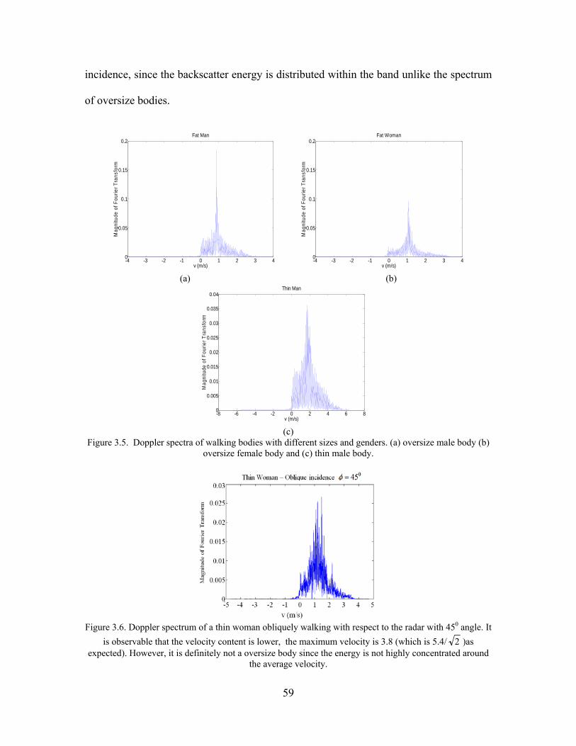
59
incidence, since the backscatter energy is distributed within the band unlike the spectrum
of oversize bodies.
-4 -3 -2 -1 0 1 2 3 40
0.05
0.1
0.15
0.2
v (m/s)
Mag
nitu
de o
f Fou
rier
Tra
nsfo
rm
Fat Man
-4 -3 -2 -1 0 1 2 3 40
0.05
0.1
0.15
0.2
v (m/s)
Mag
nitu
de o
f Fou
rier
Tra
nsfo
rm
Fat Woman
(a) (b)
-8 -6 -4 -2 0 2 4 6 80
0.005
0.01
0.015
0.02
0.025
0.03
0.035
0.04
v (m/s)
Mag
nitu
de o
f Fou
rier
Tra
nsfo
rm
Thin Man
(c)
Figure 3.5. Doppler spectra of walking bodies with different sizes and genders. (a) oversize male body (b) oversize female body and (c) thin male body.
Figure 3.6. Doppler spectrum of a thin woman obliquely walking with respect to the radar with 450 angle. It
is observable that the velocity content is lower, the maximum velocity is 3.8 (which is 5.4/ 2 )as expected). However, it is definitely not a oversize body since the energy is not highly concentrated around
the average velocity.

60
3.1.2. Radar Backscatter Analysis of a Walking Dog
The same procedure is performed for a walking dog to evaluate the Doppler spectrum.
The electric permittivity of the skin is approximated to be similar to that of humans,
while the effect of a 1 cm layer of thick hair covering the skin can be modeled as a
homogeneous anisotropic medium with the effective permittivity eff . This effective
permittivity can be obtained from a dielectric mixing formula for a medium composed of
thin vertical cylinders, representing hair stands, in air background. Using the Polder-van
Santen Formula [39] the values of eff for TE and TM waves are calculated from
airhairairhairaireff
airhairaireff
fTE
fTM
2)(:
)(:
(21)
Where, f is the volume fraction of hair which is approximated by 10%.
By the same token, for this target the radii of body’s curvatures is much larger than the
wavelength, hence PO method is valid. As the number of frames is not enough like the
human case, we interpolate between adjacent frames and generate 6000 frames for the
walking dog. The smaller number of frames is mainly because the dog is walking more
slowly than the human.
The electric current distribution on the dog’s face is shown in Figure 3.7 for the
illumination from the front side. Similar to the human body, the current distribution here
is maximum on facets which are more perpendicular to the wave vector. Figure 3.8 (a)
shows the Doppler spectrum of the walking dog versus velocity ( )2/( 00 k ). It is
observed that velocities spread from -0.2 m/s to 2.5 m/s while the average is around 0.8

61
m/s. Therefore, the range of periodic motion in dog is smaller than human body as
expected. The Doppler spectrum of the walking human body is presented in Figure 3.8
(b) for comparison. Comparing the Doppler spectra of walking human and dog
demonstrates major distinctions in maximum, minimum and average velocities as well as
the amplitudes. The difference between human and dog’s pattern of motion and sizes are
adequately accommodated in their Doppler spectra, giving rise to a measure for making
distinction between these targets.
Figure 3.7. Current distribution on some parts of dog’s face.
(a) (b)
Figure 3.8. (a) Doppler spectrum of scattering amplitude of a walking dog versus velocity )2/( 00 k . It can
be seen that it has peaks around its average velocity (v=0.8 m/s) and the maximum and minimum velocities are2.5 m/s and 0.2 m/s (b) Doppler Spectrum of human body presented in the previous report.
-8 -6 -4 -2 0 2 4 6 80
0.005
0.01
0.015
0.02
0.025
0.03
V (m/s)
Am
plitu
de
minimum -0.2 m/s
average 0.8 m/s
maximum 2.5 m/s
-8 -6 -4 -2 0 2 4 6 80
0.005
0.01
0.015
0.02
0.025
0.03
/2k0
Mag
nitu
de o
f Fou
rier Tra
nsfo
rm
minimum -1 m/s
average 1.8 m/s
maximum 5.4 m/s

62
As a result, the identity of a walking body can be estimated to a good extent from its
Doppler spectrum. While high RCS determines the size and gender of the body, the
bandwidth and the average velocities give a hint about the body weight and the pattern of
walking. Hence, a Doppler spectrum is capable of characterizing a target in motion very
efficiently.
3.2. Radar Backscatter Decomposition
The Doppler spectrum was shown to be a good figure of merit to recognize the type of
the moving targets. A more challenging question is whether the backscatter data can be
used for detecting conceal objects carried by individuals. The concealed carried objects
such as handguns and firearms are most commonly carried on the torso and thus it is
essential to investigate the response of the torso to investigate the detection of concealed
objects. Since the total spectrum of walking human body is a combination of the
individual parts’ spectra, the goal is to extract the response of torso from the rest of the
body.
Here we explore the feasibility of detecting body-attached irregular objects by
decomposing the overall backscatter response in terms of its origin from different body
parts. As mentioned before, since the shapes of most concealed objects unlike human
body are not symmetric and smooth at W-band, they can enhance cross-polarized
response. However, when the body is moving, cross-polarized backscatter is increased
since concave surfaces are formed and the interactions between different body
components are increased. On the other hand, as the concealed objects are commonly

63
carried near the torso, and noting that torso is convex and does not generate significant
cross-polarized backscatter response, the polarimetric signature of torso alone may
provide the necessary information for detecting concealed objects.
The backscattering response of the torso is dominated by the single-bounce backscatter
mechanism and its polarimetric response resembles that of a sphere. To analyze the
polarization response of the torso, first the polarimetric backscattering response is
calculated and the responses of Shh, Svh, and Shv are normalized by Svv. Then the Muller
matrix is calculated as follows [29]
11][ WRRM T (22)
where,
jj
R
00
1100
0011
0011
****
****
****
****
hhvvhvvhhhvhhvvv
vhhvvvhhvhhhvvhv
hhhvhvhhhhhhvhhv
vhvvvvvhvhvhvvvv
SSSSSSSS
SSSSSSSS
SSSSSSSS
SSSSSSSS
W
(23)
The elements of Muller matrix are averaged all angles of illumination. To simulate the
response of torso for any arbitrary combination of polarizations, the synthesized
polarization response ),( P is calculated from
TSMSP ),( (24)
where,
)2sin()2cos()2sin()2cos()2cos(1 S (25)

64
and and are the orientation angle which ranges from 90 to 90 and the ellipticity
angle which ranges from 45 for left-hand to 45 for right-hand circular polarization.
The polarization response of the torso in represented in Figure 3.9 in comparison with
that of sphere. It is observable that the co-polarized response is maximum for linear and
minimum for the circular polarizations, which is similar to that of a sphere. The only
difference is that the response of torso is slightly higher for vertical polarization.
In the presence of an external irregular object the polarimetric backscatter will undergo
a change that can be used for detection. The change in the polarimetric backscatter from
the torso and the external object results from the direct backscatter of the object and its
interaction with the torso (shadowing and multiple scattering). Hence by isolating the
polarimetric response of torso, it is possible to detect the existence of concealed irregular
objects.
(a)
(b)
Figure 3.9. (a) Polarization response of sphere and (b) torso.

65
Since all spectra of body components are overlapping, we cannot isolate the spectrum
of the torso by simple filtering. One can attempt to use simple models to create a matched
filter for the moving parts, but due to the complex shape and motion of the body parts and
their motions, such matched filters are incapable of separating the desired radar
responses. We have explored an approach to extract the response of the torso based on
the temporal deviations in the RCS response for the body during walking and the time-
frequency analysis. In this approach, complex time varying responses from the limbs are
removed from the overall backscatter to isolate the response of the torso.
3.2.1. Temporal Variation of Body RCS
To isolate the response of the torso from the full body, we can take advantage of the
variations in the response of legs and arms during walking. While the torso response is
nearly constant at different instances of walking, the responses of the limbs undergo a
major change due to considerable differences in their orientation and position with
respect to the radar. At instances when the limbs are spread out a lower backscattering
response from the limbs is expected since their projected cross-section in the beam is
smaller and, more importantly, the specular reflection from most facets are away from the
backscatter direction. On the other hand, when the limbs are aligned with the body, their
physical cross-section is higher and there are many facets with their specular reflection in
the backscatter direction. Figure 3.10 shows the backscattering response of limbs at
different instances of walking positions. As predicted, it is observed that the limbs
backscatter is lower at the moments when the limbs are spread out (when the axial
orientation is such that the specular component of the scattered field is away from the

66
backscattering direction) and is higher when they are aligned with the body. Figure 3.11
represents the walking body at different positions. It is shown that at t = 0.15 s and t =
0.65 s the limbs are spread out and their RCS is lower as shown by Figure 3.10.
Similarly, around t = 0.4 s and t = 0.9 s, the limbs are aligned with the body and their
backscatter response is higher.
It is also interesting to compare the backscatter responses of the torso and limbs at
different walking positions. Table IV presents the RCS of the torso, RCS of limbs and
their ratio at the same walking positions shown in Figure 3.11. It shows that the responses
of the limbs are lower at t = 0.15 s and t = 0.65 s, therefore the ratio of the torso response
to the limbs’ response is high. Similarly, at t = 0.4 s and t = 0.9 s, the response of legs
and arms are significantly higher, so that the ratio of the response of the torso to the limbs
is much lower. The amount of difference in RCS represents a sufficient contrast in
motion detection.
The response of the torso does not undergo a significant change during walking due to
its minimal motion during walking. This feature can be utilized to isolate the response of
limbs from the rest of the body. The response of the body at the moments when the cross-
section of legs and arms are small can be mainly attributed to the torso. For example, the
response of the body between 0.1s ~ 0.2s and 0.6 s ~ 0.7 s (almost 20 % of the walking
time) can be considered the contribution of the torso to a large extent.
The Torso RCS (dBsm) The Limbs RCS (dBsm) Ratio t = 0.15 s -6.0208 -18.4051 +12.3843 t = 0.4 s -7.075 +3.964 -11.0387
t = 0.65 s -4.5727 -11.6678 +7.0951 t= 0.9 s -7.2096 +4.1284 -11.3379
Table IV. The RCS of the torso and legs and arms and also their ratio at four sample positions where the
legs and arms either aligned with torso or are spread out.

67
0 0.1 0.2 0.3 0.4 0.5 0.6 0.7 0.8 0.9 1-60
-50
-40
-30
-20
-10
0
10
time (s))
Legs
and
arm
s R
CS
(dB
sm)
Figure 3.10. Backscattering response of the legs and arms during walking for different walking positions. It is lower when they are spread out (t = 0.15 s, t = 0.65 s) and higher when they are aligned with the body (t
= 0.4 s, t = 0.9 s).
Figure 3.11. The position of human body during walking at different time frames (approaching the radar). It is observable that around t = 0.15 s and t = 0.65 s where the legs and arms are spread out, the RCS of legs and arms are lower as shown by Figure 3.10. Similarly, around t = 0.4 s and t = 0.9 s when the legs and
arms are aligned with the body, the response is higher.
3.2.2. Time-Frequency Analysis
During walking, there are moments at which limbs’ velocities have the most difference
with the velocity of the torso. This of course can also be observed in the radar backscatter
Doppler spectra if time-frequency analysis is used. To capture the temporal spectra, the

68
time domain backscatter signal is divided into a number of sub-signals over an
appropriate time interval. Each of these signals represents a time frame (with 0.01 s
length) during walking. The Fourier transformation is then performed on these sub-
signals, yielding a set of spectra in discrete time steps. To avoid spurious response in the
frequency domain, the backscatter signal in time domain is multiplied by a series of
shifted overlapping Gaussian signals as shown in Figure 3.12. These signals are Fourier
transformed and the result is shown in the two-dimensional plots of Figure 3.13 (a) for
the thin female model. The observed time domain spectra of backscatter signal reveals
detailed features of walking positions. If the selected frames happen to be at the moment
where the limbs have their maximum velocities (limbs aligned with the torso), the
spectrum is wide and centered around the average velocity for the torso ( 8.1 m/s). At
another instance, when the legs and arms velocities are minimum, the spectrum is
narrower. In this situation, as presented in the previous section, the response of the limbs
is about 20 dB lower. In Figure 3.13 (b) and (c) the time-frequency responses of the limbs
and torso individually are presented. It is shown that around t = 0.15 s and t = 0.65 s, the
bandwidth of the limbs spectrum is narrow, has lower level, and is centered around the
torso’s average velocity. On the other hand, when limbs have their maximum velocities,
their spectrum is wideband. In this case the total backscatter power is higher, but spread
out in the spectrum. Hence there seems to be two approaches to isolate the response of
the torso, one is to identify the frame where bandwidth is minimum, and the other one is
to identify the frame where the bandwidth is maximum and filter out the high and low
frequency components. Figure 3.14 shows two temporal backscatter responses: 1) the
response of the body when the spectrum is narrow (around t = 0.15s), and 2) the response

69
of the body when the spectrum is wideband (around t = 0.4s). A Gaussian bandpass filter
centered at 1140 Hz (corresponding to 1.8m/s) and 3-dB band width of 210 Hz is used to
isolate the response of the torso. The filtered responses of the frames closely resemble
that of the torso alone at both instances. This method can be used to isolate the response
of the torso from the rest of the body for detecting concealed objects around the torso as
presented in the next section. It should also be noted that the small differences in the
response of the torso in Figure 3.14 (a) and (b) are due to the fact that the posture of the
torso itself varies a small amount during walking.
0 0.005 0.01 0.015 0.02 0.025 0.03 0.035 0.04 0.045 0.05-0.8
-0.6
-0.4
-0.2
0
0.2
0.4
0.6
0.8
1
time (s)
scat
terin
g am
plitu
de
Figure 3.12. The signal is multiplied by a number of shifted Gaussian functions.

70
(a)
(b) (c)
Figure 3.13. The co-polarized response of the human body is Fourier transformed using time-frequency analysis. (a) full body (b) the limbs and (c) the torso. The signal is chopped into a number of sub-signals
using a number of shifted Gaussian signals and the Fourier transformed is performed on the resulting sub-signals. The plots show different bandwidths for different frames. For the full body, while there are
moments (around t = 0.4 s and t = 0.9 s) in which the velocity of the legs and arms are maximum and bandwidth is wide, there are some other times (around t = 0.15 s and t = 0.65 s) that their velocity is
minimum and the bandwidth is narrow. The bandwidth of the limbs’ spectrum is narrow around t = 0.15 s and t = 0.65 s and confined around the same velocity as torso is located. At other moments, when legs and
arms have higher velocities, their spectrum is wideband and spread out, while the spectrum of torso is narrow around the middle-velocity at all times.

71
-1 -0.5 0 0.5 1 1.5 2 2.5 3-80
-70
-60
-50
-40
-30
-20
v (m/s)
Sca
tterin
g A
mpl
itude
(dB
)
full body torsofiltered full body
-1 -0.5 0 0.5 1 1.5 2 2.5 3-70
-60
-50
-40
-30
-20
-10
v (m/s)
Sca
tterin
g A
mpl
itude
(dB
)
full bodytorsofiltered full body
(a) (b)
Figure 3.14. Temporal backscattering response of torso and the full body at two instances: (a) the limbs are spread out and the spectrum is narrow. (b) the limbs are aligned with the body and the spectrum is wide.
The filtered response of the full body resembles that of the torso at both instances.
3.2.3. Polarimetric Time-Frequency Analysis for Detection of
Concealed Objects
As mentioned before, the backscatter response of the torso does not generate any
substantial amount of cross-polarized backscatter. On the other hand, the irregular shape
of most concealed objects, such as handguns and firearms, can produce a noticeable
amount of cross-polarized backscatter response. Also, when a weapon is carried on the
torso, the interaction between the torso and the object can generate cross-polarized
response as well. This feature can be exploited to detect concealed objects. The procedure
for isolating the torso response from the limbs was described in the previous section. We
can apply this technique to the fully polarimetric backscatter response and isolate the
polarimetric response of the torso alone. The polarimetric radar backscatter analysis is
based on examining the ratio of cross-polarized/co-polarized response to explore the
presence of objects. To examine the performance of this approach, simulation of a human
body with a generic handgun attached is carried out.

72
To begin with, the gun model is incorporated over the human model mesh as shown in
Figure 3.15. The gun is moved with the moving body by having it anchored to one of the
facets of the waist. Since the handgun is made of metal, a perfect electric conductor
boundary condition is used.
The iterative PO model is used to analyze the polarimetric radar backscatter response
of the handgun and human body including all interactions up to the third order in the
vicinity of the gun. The time-frequency analysis is applied to both co- and cross-polarized
responses to isolate the response of the torso. For this purpose, from the time-frequency
signal, the instances with maximum and minimum bandwidths are found. Then the signal
is filtered around the average velocity of the body in order to isolate the response of the
torso. The ratios of cross- to co-polarized responses for the isolated the torso for two
cases (with and without the handgun) is investigated. Table V shows the results for the
two instances, one where
Figure 3.15. the gun is placed on the human waist where a handgun is actually carried.

73
cross- to co-polarized response
Without hand gun (dB)
With handgun
(dB)
Ratio (dB)
spread-out position (narrow bandwidth, t = 0.15)
-15.4 -8.23 +7.17
aligned position (wide bandwidth t = 0.4 s
-21.1 -17.58 +3.52
the entire body without using time-frequency analysis
-18.6 -18.11 +0.5
Table V. cross- to co-polarized response of the walking human body at two instances, where the limbs are aligned with the body and where they are spread out. The response is increased when the handgun is
present.
the spectrum is narrow and the other where the spectrum is wide. It is shown that the ratio
is increased up to around 7 dB for the case where the limbs are spread out and around 3.5
dB for the case where the limbs are aligned with the body indicating improved detection
for the former case. To demonstrate the overall improvement achieved, the ratio of the
cross- to co-polarized backscatter ratios in the presence and absence of the handgun
without applying time-frequency analysis, is calculated and included in Table V. As
shown in the table, the cross- to co-polarized response of the entire body is only around
0.5 dB higher when the handgun is present which is not high enough to be used as a
means of detection. This highlights the fact that the combination of radar polarimetry in
conjunction with the time-frequency analysis can lead to the detection concealed metallic
objects at a standoff location without the need for high resolution imaging which is the
common practice. It should also be noted that since a Doppler filter is applied to the
backscatter data, all stationary objects that can produce cross-polarized response are also
filtered out. This adds to the robustness of the algorithm and can drastically reduce false
alarm rate.

74
3.3. W-band RCS Measurement
To verify the increase in the cross- to co-polarized response due to the presence of a
handgun, a paper-mache model of upper thigh, torso and head was made with focus on
textural smoothness. The surface is covered with a material with skin dielectric constant
as shown in Figure 3.16 . The measured polarimetric response of torso with and without a
handgun is performed with this dummy. For this purpose, it is mounted atop of a
turntable which turns from 00 to 3600 and the radar measures the polarimetric response at
each position. The University of Michigan 95 GHz fully polarimetric radar is used to
measure polarimetric response of the dummy in the anechoic chamber. The measurement
setup is shown in Figure 3.17.
Figure 3.16. Paper-mache model of upper thigh, torso and head.
.
75
Figure 3.18 shows the polarimetric responses of torso with and without a handgun. It is
shown that presence of the gun enhances the amount of cross-polarized response from the
torso up to 10 dB. This verifies the fact that the presence of irregular external objects
enhances the cross-polarized response of human body.
Figure 3.17. W-band RCS measurement setup for human body. It is mounted on top of a turntable.
-60
-40 dB
-20
80
30
210
0 dB
240
90
270
120
300
150
330
180 0
vvhhvhhv
(a) (b)
Figure 3.18. Polarimetric response of torso is measured using a 95 GHz radar (a) without and (b) with a handgun.It is observable that the presence of the firearm increases the cross-polarized response
turntable

76
3.4. Radar backscatter Analysis of Human Body at Y-band (220- 325 GHz)
One of the main advantages of radar backscatter analysis of moving objects at MMW
frequencies is the higher recognition capability for slowly moving objects. The
bandwidth of the Doppler spectra of complex moving targets such as human body
becomes wider as the frequency is increased. However, in terms of velocity content it
does not changed. In order to fully understand the effect of radar frequency in the
Doppler spectrum, the thin female body is analyzed at higher Y-band range (220-325
GHz). The qualitative current distribution on the body is shown in Figure 3.19 (a) and
presents variations very similar to those in W-band. The Doppler spectrum shows similar
variations with a wider bandwidth from -1600 Hz to 8600 Hz. However, the velocity
content remains the same as shown in Figure 3.19 (b). The only obvious difference is the
amplitude of the RCS which is around 40% lower compared to the results in W-band.
This is due to the fact that skin dielectric constant is lower at Y-band compared to W-
band.
(a) (b) Figure 3.19. (a) The qualitative current distribution on human body and (b) the Doppler spectrum of
walking at 240 GHz.
-8 -6 -4 -2 0 2 4 6 80
0.002
0.004
0.006
0.008
0.01
0.012
0.014
0.016
v (m/s)

77
Figure 3.20. The required antenna beamwidth to provide footprints commensurate to human body width.
Y-band frequency range can also be used for the proposed detection algorithm. The
chance to have higher co-polarized response for the human body and therefore enhanced
cross- to co-polarized response at the presence of irregular objects might be higher, which
makes the algorithm more robust. In addition, for standoff detection, antennas with very
narrow beamwidth are required to provide footprints commensurate to human body at
very large distances. For example, at 200 m range, for an average-size human body width
(50 cm width), ϕ = 1tan (0.5 / 200) 0.0025 rad. At W-band the required antenna
aperture to realize such a beamwidth is / 0.0025 / 0.0025D D = 3 mm / 0.0025
= 1.2 m which is large, while at Y-band it becomes three times smaller: / 0.0025D =1
mm / 0.0025 = 40 cm. It should be noted that the length of the aperture for the human
height is around 3.5 times smaller in each case.
If the antenna aperture length is one third smaller, the aperture area will be 1/9 times
smaller and the weight will be 1/27 lighter which results in more compact and light-
weight systems. On the other hand, since the wavelength is around 1mm, the dimensions
of the waveguide structures are in the order of hundreds of micron. This makes the band
suited for micromachining applications. Moreover, Y-band compared to W-band is
underutilized and the available bandwidth is much higher. Mature technologies are
available at W-band and many technological problems have already been solved, whereas
ϕ
1.8 m
0.5 m
200 m

78
at Y-band, many concerns regarding sources and amplifiers for MMIC technology should
still be addressed and solved. Y-band radars require technological advances to be well-
suited for navigation and obstacle detection. These motivate the development of a Y-band
radar which can be later enhanced for polarimetric applications and concealed target
detection.
3.5. Conclusion
In this chapter, the radar backscatter responses of walking human bodies at W-band
were calculated. This sequence of the backscatter response generates a time domain
signal which is Fourier transformed to derive the Doppler spectrum of the target. The
feasibility of identifying different body sizes/genders and walking dog based on the
characteristics of the Doppler spectra were investigated. Then a radar backscatter
decomposition algorithm was presented to isolate the response of torso in order to be able
to measure the cross-polarized the response of torso. It was verified that the higher cross-
to co-polarized response of torso is an indication of the presence of irregular external
object. The RCS measurement of the human torso at the W-band is then presented and
verifies the enhancement of the cross- to co-polarized response at the presence of an
irregular object. The radar backscatter analysis of the walking human body at Y-band was
then presented which motivates the phenomenological studies at Y-band. This
necessitates the realization of high resolution radars at Y-band.
3.
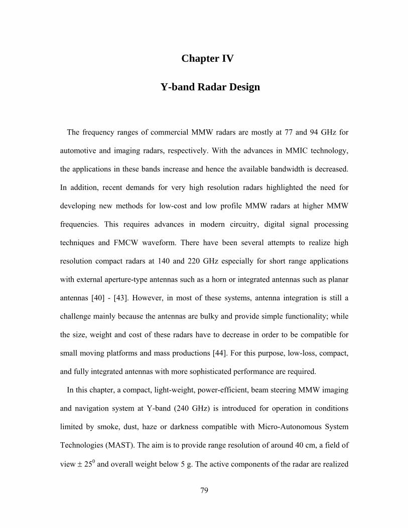
79
Chapter IV
4. Y-band Radar Design
The frequency ranges of commercial MMW radars are mostly at 77 and 94 GHz for
automotive and imaging radars, respectively. With the advances in MMIC technology,
the applications in these bands increase and hence the available bandwidth is decreased.
In addition, recent demands for very high resolution radars highlighted the need for
developing new methods for low-cost and low profile MMW radars at higher MMW
frequencies. This requires advances in modern circuitry, digital signal processing
techniques and FMCW waveform. There have been several attempts to realize high
resolution compact radars at 140 and 220 GHz especially for short range applications
with external aperture-type antennas such as a horn or integrated antennas such as planar
antennas [40] - [43]. However, in most of these systems, antenna integration is still a
challenge mainly because the antennas are bulky and provide simple functionality; while
the size, weight and cost of these radars have to decrease in order to be compatible for
small moving platforms and mass productions [44]. For this purpose, low-loss, compact,
and fully integrated antennas with more sophisticated performance are required.
In this chapter, a compact, light-weight, power-efficient, beam steering MMW imaging
and navigation system at Y-band (240 GHz) is introduced for operation in conditions
limited by smoke, dust, haze or darkness compatible with Micro-Autonomous System
Technologies (MAST). The aim is to provide range resolution of around 40 cm, a field of
view 250 and overall weight below 5 g. The active components of the radar are realized

80
on CMOS and InP, while the passive components are realized on hollow waveguides to
reduce weight and loss. The radar antenna is a frequency scanning array using rectangular
waveguide structure integrable with the active chips. This motivates the utilization of
micromachining to fabricate and integrated the radar component. The technique provides
easy fabrication of structures with micron-range dimension control and further reduction
of the cost. A basic block diagram of the Y-band radar is presented in Figure 4.1 and the
specifications are listed in Table VI.
Figure 4.1. Block diagram of the Y-band FMCW radar.
Wavelength 1.2 mm
Peak Tx power 10 dBm Rx Sensitivity with 5 dB
SNR -135 dBm
Beamwidth Az: 20
El: 80
max directivity 27 dB
Polarization Vertical Volume 2 cm
3
Weight 5 g
Field of View 25deg
Range Resolution 37.5 cm
Table VI. Radar specifications.

81
4.1. Components
Signal Generator
Depending on the application, the radar transmit signal can be pulse or CW. CW
transmissions employ low continuous power compared to the high peak power of the
pulsed radars. However, CW radars using unmodulated waveforms cannot measure the
target’s range [45]. The issue is addressed by frequency or phase modulation of the
signal. The frequency modulated CW signal (FMCW) has many advantages over pulse
radars. They spread the transmitted energy over a large modulation bandwidth providing
good range resolution and their circuitry is well-matched to solid-state transmitters
leading to low cost and high reliability systems. The purpose of the radar, and the
expected characteristics of the targets, in addition to the demands of moving target
indication (MTI) and electromagnetic compatibility (EMC) are some of the factors that
determine waveform design. For the Y-band radar, a CMOS digital VCO with 12 bit 50
MS/s ADC is implemented in 65nm CMOS to generate the FMCW signal at 20 GHz. The
waveform generated by VCO is a stepped FMCW signal. To design the waveform, first
the number of the required frequency steps and bandwidth is calculated. For ± 250 = 500
beam steering and 20 of beamwidth, 25 frequency steps are required to cover the field of
view. The frequency range of 230 ~ 245 GHz is chosen for beam steering. Hence,
MHz/step600steps25
GHz15 .
The radar is mounted on a moving platform and depending on the application; the
platform could be a flyer, rover or crawler. The frame should be updated faster for fast
platforms; therefore the VCO should be able to adaptively change the frame update rate
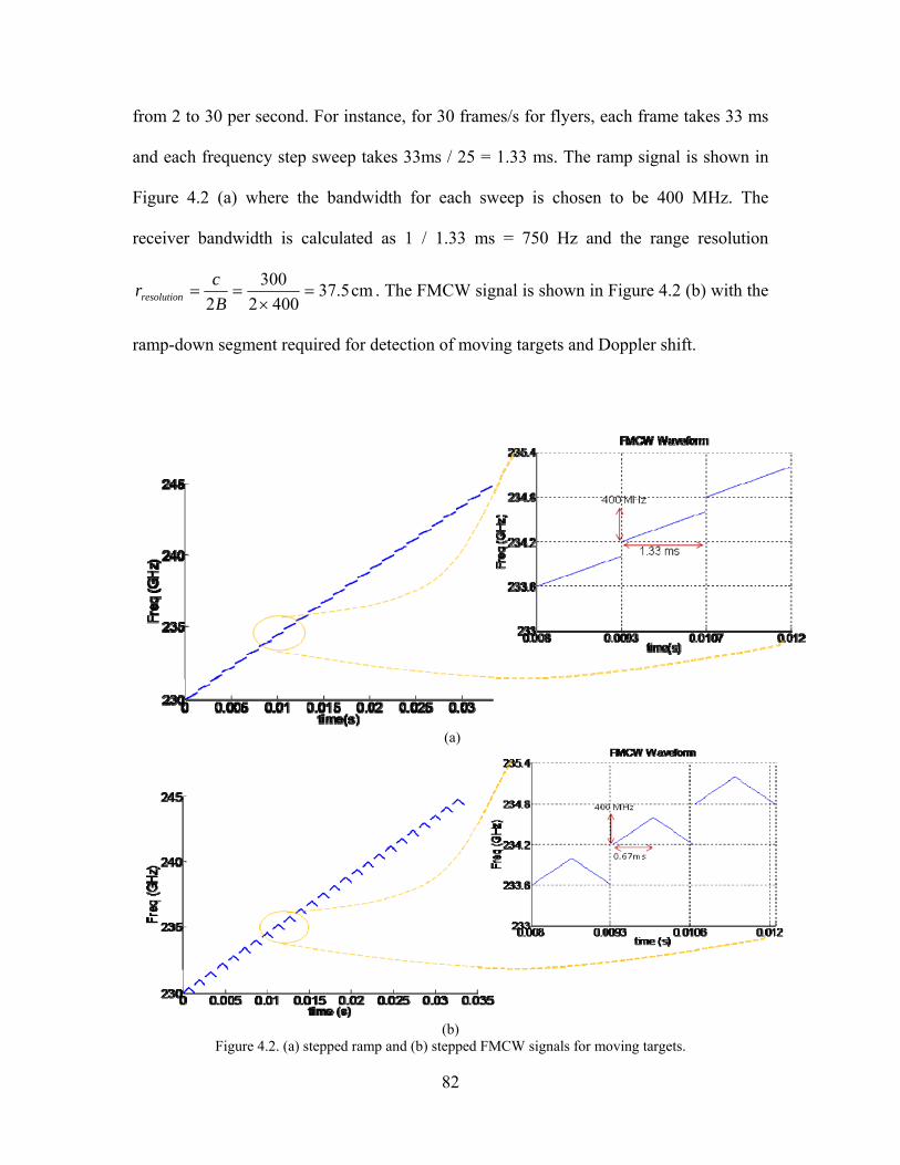
82
from 2 to 30 per second. For instance, for 30 frames/s for flyers, each frame takes 33 ms
and each frequency step sweep takes 33ms / 25 = 1.33 ms. The ramp signal is shown in
Figure 4.2 (a) where the bandwidth for each sweep is chosen to be 400 MHz. The
receiver bandwidth is calculated as 1 / 1.33 ms = 750 Hz and the range resolution
cm5.374002
300
2
B
crresolution . The FMCW signal is shown in Figure 4.2 (b) with the
ramp-down segment required for detection of moving targets and Doppler shift.
(a)
(b)
Figure 4.2. (a) stepped ramp and (b) stepped FMCW signals for moving targets.

83
Transmitter
The main components in transmitters are the up-converting mixer or frequency
multiplier, filters and the power amplifier. The IF signal is converted into the RF
frequency signal by mixers or frequency multipliers. The undesired harmonics and
images are attenuated using bandpass filters. Finally the power amplifier provides
amplification for the transmit signal before it excites the antenna. Couplers are commonly
used to provide a sample of the transmit signal or the LO for the receiver down-
convertor. To provide a 240 GHz signal for the antenna, the VCO signal frequency is
first doubled twice using frequency doublers fabricated with non-linear passive or active
devices. Schottky diodes on FET can be used as the nonlinear device to generate the
second harmonic because of their high cutoff frequency and square-law characteristics.
Band-pass filters for harmonic elimination and amplifiers are used after each step of
frequency doubling. At the next step a frequency tripler is used to convert the 80 GHz
signal to 240 GHz and then amplified with a power amplifier fabricated with high-
frequency HEMT transistors.
Receiver
The receiver subsystem takes the signal from the antenna and passes it to the low-noise
amplifier (LNA). The system generally consists of LNA, down-converting mixer, filter
and IF amplifier. If the transmit and receive antennas are identical, duplexers are used to
provide isolation between transmit and receive signal. In addition to the image rejection,
filtering in the receiver is used to attenuate interference from other radars or high-
powered electrical devices during reception. Receiver noise figure and minimum
detectable signal are critical parameters of the receiver subsystem. The minimum
84
detectable power depends on the signal to noise ratio and thermal noise power and affects
the maximum detectable radar range.
The LNA is fabricated with HEMT transistors similar to the PA. A sample of the
transmit signal is mixed with the output signal of the LNA and generates the baseband
signal. Filter and amplifier are used to remove the higher order harmonics and
interferences and to amplify the baseband signal.
Baseband
Almost all modern radars use digital signal processors to perform processing operations
such as correlation, Doppler filtering, image rejection, detection processing and tracking.
To provide signal for digital processing, A/D converters are placed at the end of the
receiver signal path. Data processors are used to convert data produced by the signal
processor into a form that is readily interpretable by radar operators.
A low-power processor is used to extract the frequency content of the signal. ADC and
FFT modules are important parts of the processor with a developed circuit design
techniques to enable high circuit activity and peak energy efficiency during FFT
computation.
4.2. Antenna
Most systems employ separate antennas for transmit and receive in order to provide
better isolation. According to the radar equation [46], if the maximum radar range rmax is
defined for the receiver minimum detectable signal Smin, according to radar equation

85
43
min
2
max )4(
S
GGPr rtt
(26)
where, Pt is the transmit signal power, Gt and Gr transmit antenna gain, and the target
RCS. A detectable signal must be larger than the noise (5 to 10 dB higher). Smin can be
expressed in terms of signal to noise ratio (S/N) required for a reliable detection times to
the receiver noise:
nn BFTkNSPN
SS 00min (27)
where k0 is Boltzman’s constant, T is the temperature B is the receiver bandwidth and Fn
is the receiver noise figure. If S/N = 5 dB, Fn = 5 dB and B = 750 Hz:
Smin (dBm) = 5 174 +10 log (B) + Fn (dB) = 135 dBm
To prevent aliasing during RCS measurements the range should be alias-free. The
alias-free range is a distance from the radar that a target response appears with the
accurate range. Since in FMCW waveform the target range is proportional to the
periodicity of baseband signal (T) and to the inverse of pulse repetition frequency, the
range function is also periodic and a target outside alias-free range may appear much
closer to the radar. If the baseband signal is sampled N times over one period and a chirp
bandwidth of F is used, the maximum frequency content is limited to N / T. Noting that
for FMCW radar range and frequency shift are linearly dependent, the maximum alias
free range is given by

86
F
NcR
2max (28)
The range resolution of the radar can be related to the alias range:
resolutionNrF
NcR
2
(29)
For a known value of alias-free range and range resolution, the number of sampling
point can be evaluated.
Antenna maximum directivity can be approximated by A4
, where ΩA is the beam
solid angle and is defined as the solid angle in which if the antenna radiation intensity is
constant (and maximum value), all power would flow through it. In the case of antennas
with one narrow major lobe and very negligible minor lobes, the beam solid angle can be
approximated as the product of the half-power beamwidths in two perpendicular planes, i.
e., azimuth and elevation angles elevationazimuth
4
. The antenna maximum gain is defined
as maximum directivity times the antenna efficiency. The radar antenna should provide
narrow beams in azimuth and elevation directions (20 and 80); therefore, the maximum
directivity is estimated as Dmax = 34 dB. If the antenna efficiency is 7 dB, the maximum
gain of the antenna is 27 dB.
With Smin = 135 dBm, Pt= 10 dBm, Gt= 27 dB, and 26.1 mm, according to Eq. (26),
the radar range is represented in Figure 4.3 versus target RCS. The RCS of some know
targets such as metal spheres, dry wall, concrete wall, and a human body at that
frequency range are presented for comparison.
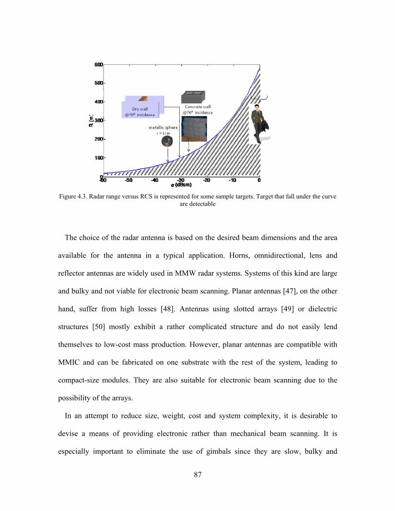
87
Figure 4.3. Radar range versus RCS is represented for some sample targets. Target that fall under the curve
are detectable
The choice of the radar antenna is based on the desired beam dimensions and the area
available for the antenna in a typical application. Horns, omnidirectional, lens and
reflector antennas are widely used in MMW radar systems. Systems of this kind are large
and bulky and not viable for electronic beam scanning. Planar antennas [47], on the other
hand, suffer from high losses [48]. Antennas using slotted arrays [49] or dielectric
structures [50] mostly exhibit a rather complicated structure and do not easily lend
themselves to low-cost mass production. However, planar antennas are compatible with
MMIC and can be fabricated on one substrate with the rest of the system, leading to
compact-size modules. They are also suitable for electronic beam scanning due to the
possibility of the arrays.
In an attempt to reduce size, weight, cost and system complexity, it is desirable to
devise a means of providing electronic rather than mechanical beam scanning. It is
especially important to eliminate the use of gimbals since they are slow, bulky and

88
susceptible to mechanical failure as they experience strong mechanical forces that sharply
limit the scanning speed [51] - [54]. One the other hand, electronic beam steering radars
are fast but rather expensive and power inefficient, requiring several Watts of power. In
addition, the incorporated phase shifters are lossy, bulky and in most cases not available
at higher MMW frequencies [55], [56].
Considering these limitations, a traveling-wave frequency scanning approach is the
simplest method of beam steering if enough bandwidth is available for the radar
operation [57]. In a traveling-wave frequency scanning antenna array, scanning is
achieved as a result of the frequency dependence of the complex propagation constant of
the wave propagating inside the waveguide. Principally, elements are fed in series with a
transmission line having an appropriate delay line segments between two adjacent
elements. As the frequency is swept the delay lines provide different values for the phase
difference and cause beam steering. Taking advantage of transmission lines to generate
the desired phase shift discharges us from using electronic phase shifters which require
additional power to operate, and reduces the cost of the overall system. Moreover, the
problem of connecting the miniature MMIC phase shifter chip to the external antenna via
a transition is solved since the phase shifters and radiating elements are now in one unit
and can be fabricated on a single substrate.
Travelling-wave antennas are designed based on either dielectric materials [58] which
result in slow wave radiation or hollow structures [59], [60] which results in fast wave
radiation. In upper MMW band, excessive conductor loss in the complex feeding
networks is a major problem. In addition, printed transmission lines such as microstrip
require very thin substrates to avoid exciting surface waves. Construction of scanning

89
arrays based on hollow waveguide structures proves to be convenient since they provide
enough bandwidth, do not incorporate dielectric materials, yet present high power
handling capabilities and lower loss especially at higher frequencies compared to planar
transmission lines. In these travelling-wave structures, the length of the waveguide
provides the desired phase shift, while the radiation is through slots cut on the walls of
the waveguide making it a leaky wave structure. Another advantage of the hollow
waveguides is their light weight which makes them attractive when a large structure like
an array is required. In addition, manufacturing such a structure at Y-band frequencies
with high resolution is feasible using bulk or surface micromachining techniques.
4.3. Fabrication/Assembly
At high MMW and SMMW bands, as the dimensions of the structures shrink, standard
machining methods are not suitable because of low fabrication tolerances and high cost in
assembly. However, micromachining offers easy fabrication of complex structures with
low cost and low mass. Although micromachining can provide the required tolerances for
fabrication of small and high precision devices, there are many limitations on what can be
fabricated. For example structures that are 2.5D in nature and structures formed by
stacking wafers with 2.5D geometries are straightforward to fabricate. Therefore, the
structures have to be simple with all its features aligned with the Cartesian coordinate
planes in order to be compatible with micromachining processes.

90
(a) (b)
Figure 4.4. (a) Bulk micromachining: the microstructure is fabricated by DRIE etching of silicon substrate [61]. (b) Surface micromachining: the microstructure is fabricated using lithography of a thick
SU-8 photoresist layer [62].
Figure 4.5. Sidewall scalloping of DRIE process
As shown in Figure 4.4, both surface micromachining which creates structures on
top of a substrate and bulk micromachining which produces structures inside a substrate
are used to create hollow structures. In surface micromachining, the microstructures are
fabricated by deposition and etching different structural layers on top of the substrate. For
very deep structures such as waveguide trenches, usually thick photoresists are used as
structural materials. The material is deposited (spun) on top of the substrate, exposed and
developed to form the structure. In bulk micromachining, the substrate itself is the
structural material. It is patterned and wet / dry etched to form the microstructure. Bulk
micromachining is more expensive and causes sloped sidewalls for wet etching and
sidewall scalloping for deep reactive ion etching (DRIE) as shown in Figure 4.5. On the
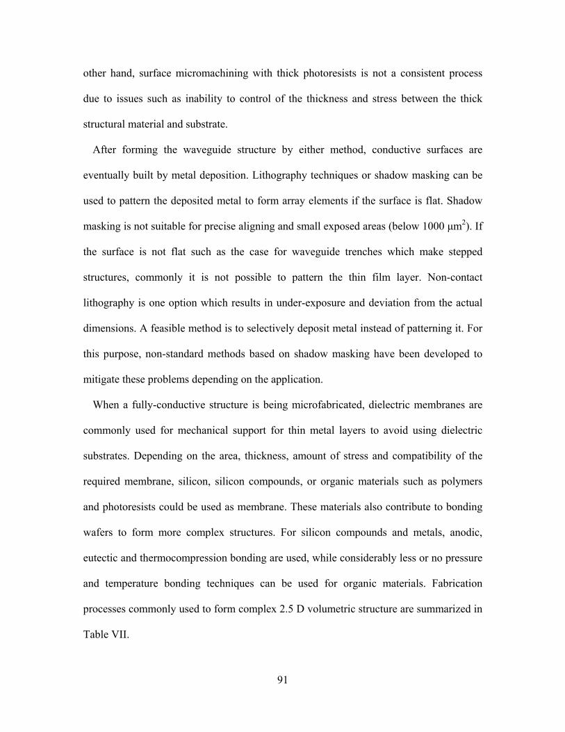
91
other hand, surface micromachining with thick photoresists is not a consistent process
due to issues such as inability to control of the thickness and stress between the thick
structural material and substrate.
After forming the waveguide structure by either method, conductive surfaces are
eventually built by metal deposition. Lithography techniques or shadow masking can be
used to pattern the deposited metal to form array elements if the surface is flat. Shadow
masking is not suitable for precise aligning and small exposed areas (below 1000 μm2). If
the surface is not flat such as the case for waveguide trenches which make stepped
structures, commonly it is not possible to pattern the thin film layer. Non-contact
lithography is one option which results in under-exposure and deviation from the actual
dimensions. A feasible method is to selectively deposit metal instead of patterning it. For
this purpose, non-standard methods based on shadow masking have been developed to
mitigate these problems depending on the application.
When a fully-conductive structure is being microfabricated, dielectric membranes are
commonly used for mechanical support for thin metal layers to avoid using dielectric
substrates. Depending on the area, thickness, amount of stress and compatibility of the
required membrane, silicon, silicon compounds, or organic materials such as polymers
and photoresists could be used as membrane. These materials also contribute to bonding
wafers to form more complex structures. For silicon compounds and metals, anodic,
eutectic and thermocompression bonding are used, while considerably less or no pressure
and temperature bonding techniques can be used for organic materials. Fabrication
processes commonly used to form complex 2.5 D volumetric structure are summarized in
Table VII.
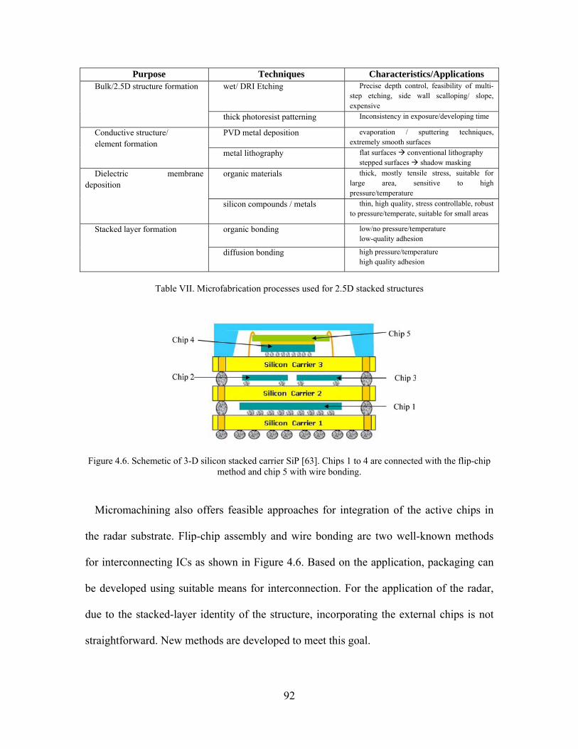
92
Purpose Techniques Characteristics/Applications Bulk/2.5D structure formation wet/ DRI Etching Precise depth control, feasibility of multi-
step etching, side wall scalloping/ slope, expensive
thick photoresist patterning Inconsistency in exposure/developing time
Conductive structure/ element formation
PVD metal deposition evaporation / sputtering techniques, extremely smooth surfaces
metal lithography flat surfaces conventional lithography stepped surfaces shadow masking
Dielectric membrane deposition
organic materials thick, mostly tensile stress, suitable for large area, sensitive to high pressure/temperature
silicon compounds / metals
thin, high quality, stress controllable, robust to pressure/temperate, suitable for small areas
Stacked layer formation organic bonding low/no pressure/temperature low-quality adhesion
diffusion bonding high pressure/temperature high quality adhesion
Table VII. Microfabrication processes used for 2.5D stacked structures
Figure 4.6. Schemetic of 3-D silicon stacked carrier SiP [63]. Chips 1 to 4 are connected with the flip-chip method and chip 5 with wire bonding.
Micromachining also offers feasible approaches for integration of the active chips in
the radar substrate. Flip-chip assembly and wire bonding are two well-known methods
for interconnecting ICs as shown in Figure 4.6. Based on the application, packaging can
be developed using suitable means for interconnection. For the application of the radar,
due to the stacked-layer identity of the structure, incorporating the external chips is not
straightforward. New methods are developed to meet this goal.

93
4.3.1. Microfabrication of Rectangular Waveguide
Microfabrication of a simple WR-3 waveguide trench as a basic component of the radar
is investigated to explore and find the most efficient techniques suitable for radar
fabrication. Most of the early work in waveguide micromachining involved creating the
waveguide height by stacking layers of etched silicon wafers. However, this technique
needs high-quality wafer-to-wafer metallic bonds in order to prevent interruption of the
current flow. There have been several attempts to fabricate W-band waveguides with
low-cost microfabrication techniques such as lithography [64], [65]. However, in these
techniques, the height of the waveguide is limited by the maximum thickness of the spun
photoresist, limiting the fabrication to the reduced-height waveguides which suffer from
high attenuation. Taking advantage of the "snap-together" technique, a rectangular
waveguide was fabricated in two halves and then the halves were put together to form a
complete waveguide ([66] - [68]). Therefore, low-cost lithography methods are first used
to fabricate a simple deep channel with vertical sidewalls.
The photoresist SU-8 from Microchem© [69] is a widely used photoresist which can be
spun up to 1 ~ 2 mm. The thickness versus spin speed of SU-8 series 2100 is shown in
Figure 4.7 (a). To achieve a WR-3 waveguide depth (approximately 432 μm), multi-step
spinning is required. A soft-bake step after each spin is necessary to help remove all the
cross-links of the polymer which might cause cracking or non-uniformity. To avoid
underexposure problems, the thickness of photoresist should be first measured precisely
using the Nano-spec (a non-contact spectroscopic-reflectometry tool used for transparent
film thickness measurements). After lithography and post-exposure bake, it is developed
in Microchem SU-8 Developer. Figure 4.7 (b) shows a meander-line waveguide trench

94
after gold sputtering. It is observed that some sidewalls are not stiff enough and broke
during development or blow dry. This can be attributed to the under-exposure or over-
development of the material or high stress between the silicon wafer and thick SU-8
layer. The thickness of the SU-8 layer is comparable to the thickness of the standard 500
μm wafers and hence the amount of stress cannot be neglected. In addition to all these
problems, with SU-8 it is not feasible to fabricate a multi-step structure needed for
waveguide transition for active component assembly. Moreover, unlike deposition
methods the thickness of the spun photoresist cannot be precisely controlled and there is
always an error in the thickness (up to 10% for multi-step spinning) involved with
spinning. The investigations showed a variety of different thicknesses (380 μm ~ 460 μm)
for different spinning conditions.
Due to all these issues, an alternative silicon DRIE approach is used to fabricate the
radar substrate. The advantages of this method compared to lithography are:
Uniformity and flatness of the surface of the substrate
Controlling the etch depth precisely by time-etching
Feasibility of consistent etch in different instances
Feasibility of fabricating multi-step structures using multiple mask layers
Robustness of the material to high pressure/temperature of bonding
CMOS-clean processing
Compatibility with non-standard packaging techniques
Diverse and selective options for etchants (wet/dry, isotropic/anisotropic)
Backside process capability needed for packaging

95
(a) (b)
Figure 4.7. (a) Thickness versus spin speed of SU-8 series 2100. (b) meander-line structure fabricated by
spinning SU-8 2100 in two steps. The structure is gold-sputtered after developing and hard-bake.
4.4. Conclusion
In this chapter, a Y-band beam steering MMW imaging and navigation radar system
was introduced for operation in conditions limited by smoke, dust, haze or darkness.
Different components of the radar and their development technology were described. The
radar antenna is a frequency scanning array using rectangular waveguide structure.
Manufacturing such a structure at Y-band frequencies with high resolution is feasible
using micromachining techniques. The compatible techniques were then introduced and
the microfabrication process of a rectangular waveguide was discussed in order to find
the most efficient method to fabricate the structure.
broken walls

96
Chapter V
5. MMW Frequency Scanning Antenna Design
The design details of the MMW frequency scanning antenna are presented and
discussed in this chapter. This includes introducing the waveguide slot array and hybrid-
coupled patch array antennas, loss and reflection minimization required for a very long
array, narrowing the beamwidth and all the limitations that should be considered to make
the structure compatible with micromachining techniques.
5.1. Design Overview
The frequency scanning array is designed using hollow rectangular waveguides where
the length of the waveguide provides the desired phase shift, while the radiation is
through slots cut on the walls of the waveguide. This one-dimensional array in the
azimuth direction makes a wide beam in the elevation direction which is not desirable.
Therefore, in order to confine the beam in the elevation direction, widening the antenna
aperture is performed using slot-coupled patch arrays as suggested in Figure 5.1. This
two-dimensional structure provides a two-dimensional confined beam.
To design a frequency scanning array based on hollow rectangular waveguides,
different configurations of slots - transverse, diagonal and longitudinal -on the narrow
and broad walls of the waveguide can be considered as represented in Figure 5.2 (a). The
frequency scanning antenna is designed for comparatively large scanning angles ( 250)
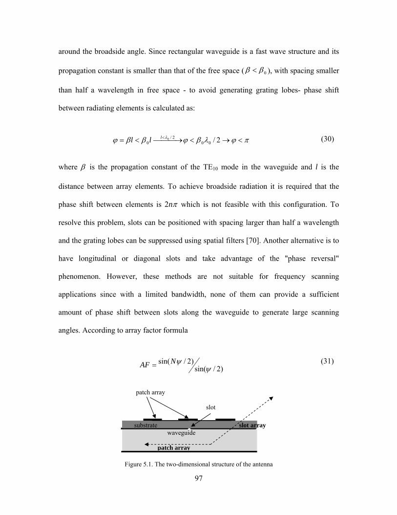
97
around the broadside angle. Since rectangular waveguide is a fast wave structure and its
propagation constant is smaller than that of the free space ( 0 ), with spacing smaller
than half a wavelength in free space - to avoid generating grating lobes- phase shift
between radiating elements is calculated as:
2/00
2/0
0lll (30)
where is the propagation constant of the TE10 mode in the waveguide and l is the
distance between array elements. To achieve broadside radiation it is required that the
phase shift between elements is n2 which is not feasible with this configuration. To
resolve this problem, slots can be positioned with spacing larger than half a wavelength
and the grating lobes can be suppressed using spatial filters [70]. Another alternative is to
have longitudinal or diagonal slots and take advantage of the "phase reversal"
phenomenon. However, these methods are not suitable for frequency scanning
applications since with a limited bandwidth, none of them can provide a sufficient
amount of phase shift between slots along the waveguide to generate large scanning
angles. According to array factor formula
)2/sin()2/sin(
NAF
(31)
Figure 5.1. The two-dimensional structure of the antenna
substrate slot array waveguide patch array
patch array
slot
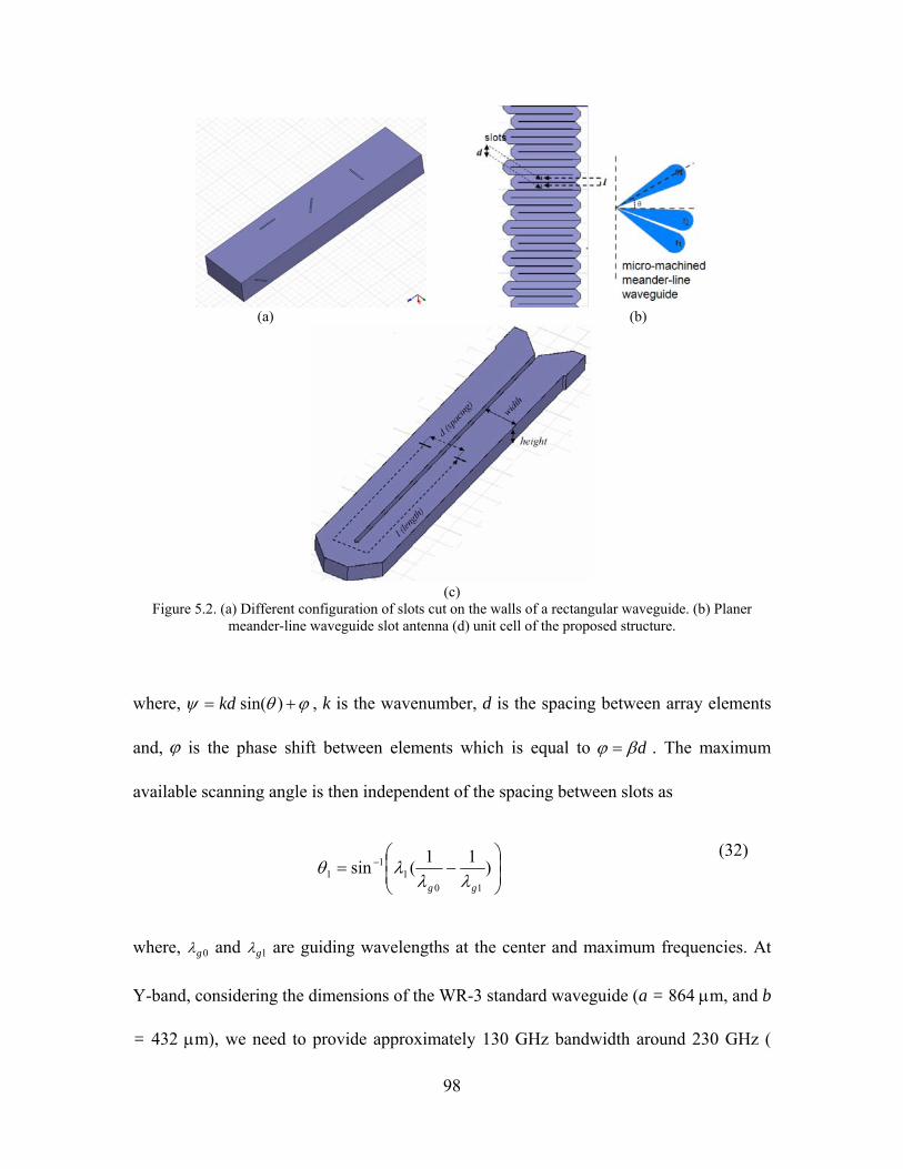
98
(a) (b)
(c)
Figure 5.2. (a) Different configuration of slots cut on the walls of a rectangular waveguide. (b) Planer meander-line waveguide slot antenna (d) unit cell of the proposed structure.
where, )sin(kd , k is the wavenumber, d is the spacing between array elements
and, is the phase shift between elements which is equal to d . The maximum
available scanning angle is then independent of the spacing between slots as
)
11(sin
101
11
gg
(32)
where, 0g and 1g are guiding wavelengths at the center and maximum frequencies. At
Y-band, considering the dimensions of the WR-3 standard waveguide (a = 864 m, and b
= 432 m), we need to provide approximately 130 GHz bandwidth around 230 GHz (

99
185 ~ 315 GHz) to achieve 250 scanning angle around an off-broadside angle (430)
which is not practical. In order to achieve broadside radiation and a satisfactory amount
of phase shift between elements without the need for a large bandwidth, we are required
to meander the waveguide which results in the increase in phase shift, while maintaining
the spacing between them a smaller quantity in order to avoid generating grating lobes as
shown in Figure 5.2 (b) and (c). In this design, the waveguide is bent around the H-plane
to have the transverse slots cut on the broad wall as the radiating elements so that
microfabrication techniques are able to manage etching the height of the waveguide
which is more achievable than etching the thick width of the waveguide. In this structure,
lkd )sin( where d is the spacing between elements which is the sum of the
waveguide width and the separating wall, while l is the length between them in each turn
as shown in the unit cell of the structure in Figure 5.2 (c). Hence, it is feasible to realize
broadside radiation at any desired frequency with nl 2 since l is flexible amd the
maximum scanning angle can also be calculated as
)
11(sin
10
111
ggd
l
(33)
To have the broadside radiation at the center frequency, l is chosen to be a modulus of
0g in order to generate n2 phase shift between the elements at the center frequency.
Table VIII shows the range of scanning angle assuming 15 GHz available bandwidth
(230 ~ 245 GHz) around the broadside radiation at 237.5 GHz for different values of wall
thicknesses and length between elements. The structure of the meander-line waveguide
requires the current distribution on the broad wall of waveguide to reverse after a turn as

100
shown in Figure 5.3. Therefore, the length between slots must be corrected by adding a
2/0g segment so that the magnetic current on the slots are in phase at the center
frequency. The additional segment increases the scanning angle as shown in Table VIII.
For the current design, t = 250m l = 5.5 0g = 1.02 cm is chosen.
To achieve a very narrow beamwidth (i.e. = 20), the length of the antenna should be
extended by using a number of the unit cells. Considering L
where, L is the aperture
length, at 230 GHz, L = 37.4 mm to achieve 20 beamwidth, which gives around 36 turns.
Since the overall waveguide length is quite large (~ 36×l = 36 cm), and a large number of
slots are involved, sources of loss and reflection from the finite conductivity of metals,
waveguide turns, and slots must be managed very carefully.
(a) (b)
Figure 5.3. The current distribution on the broad wall of the rectangular waveguide. (a) For l = n0g it is
noticeable that the direction of the electric field on the slot is reversed. (b) The reverse is compensated by adding adding a 2/0g waveguide segment.
Thickness of the separating wall
d = a + t
Length between the elements
Range of the scanning angle
t = 50 m l = 4 0g 23.30 ~ -21
t = 150m l = 5 0g 26.4 ~ -23.70
t = 250m l = 5 0g 240 ~ -21.80
t = 50 m l = 4.5 0g 26.40 ~ -23. 70
t = 250m l = 5.5 0g 26.50 ~ 23.80
Table VIII. The scanning angle of the antenna for different wall thicknesses and lengths between elements.

101
5.2. Reflection Minimization
There are two sources of reflection in the meander-line structure: the bends and the
slots. To minimize the reflection from the bends, their profile should be designed for a
minimum reflection. This can be performed by optimizing the shape of the bends using
Ansoft HFSS. Simulations results show that a diagonal cut around the edges provides a
better transmission compared to a curved turn as shown in Figure 5.4 (a) and (b).
However, even though the reflection from bends is minimized, a number of successive
small reflections from all bends add up to a considerable amount. One way to minimize
total reflection from bends is to make the distance between bends an odd modulus of
4/g at the center frequency to make a destructive interference– the two-way distance
should be a modulus of 2/g - so that the total reflection is cancelled. A unit cell of such
a structure is presented in Figure 5.5 (a) consisting of four waveguide sections. In this
structure, in order to have the slots in phase while having 4/g spacing between the
elements, the length of one of cells should be g smaller. Figure 5.5 (b) shows the
reflection coefficient of this structure. It is observed that although the reflection is
minimized at the center frequency, it is a considerable amount at other frequencies and
might cause a constructive interference and large reflection in the final structure. Figure
5.5 (c) represents the reflection coefficient for the total of nine unit cells which shows a
very high return loss around 233 and 243 GHz. Another way to minimize the total
reflection is to have constructive interference for the center frequency, since the
reflection of the bend is already minimized by optimizing the diagonal cut shown in
Figure 5.4.

102
230 235 240 245-100
-80
-60
-40
-20
Freq (GHz)
S1
1 (
dB)
Reflection Coefficient for H-Plane Waveguide Bend
diagonal cutbend
(a) (b)
Figure 5.4. (a) Electric field distribution inside the waveguide for curved and diagonal cut bends. (b) Reflection coefficient from the bends. The diagonal cut bend is 450 and lb = 0.85 mm.
In this case, the reflection in the beginning and the end of the band is minimized by
changing the thickness of separating walls (t) to make the destructive interference. The
reflection coefficient of the structure is shown in Figure 5.5 (e) and (f) for one and nine
unit cells. The maximum reflection is below -18 dB as opposed to -2 dB reflection for the
former structure, while the reflection at the center frequency is maintained around -60 dB.
This structure has thicker separating walls which makes it stiffer and suitable for
microfabrication.
To minimize the reflection of the slots, having cut one slot in each turn, the two-way
distance between two successive slots is an integer multiple of g (2×5.5 = 11 g in this
design). Therefore, their successive reflections add up coherently and causes scan
blindness at the center frequency. To mitigate this problem we need a reflection canceling
pair for each slot positioned at 4/g . A unit cell of the proposed geometry is shown in
Figure 5.6 (a). In this case, the array factor can be written as:
lb
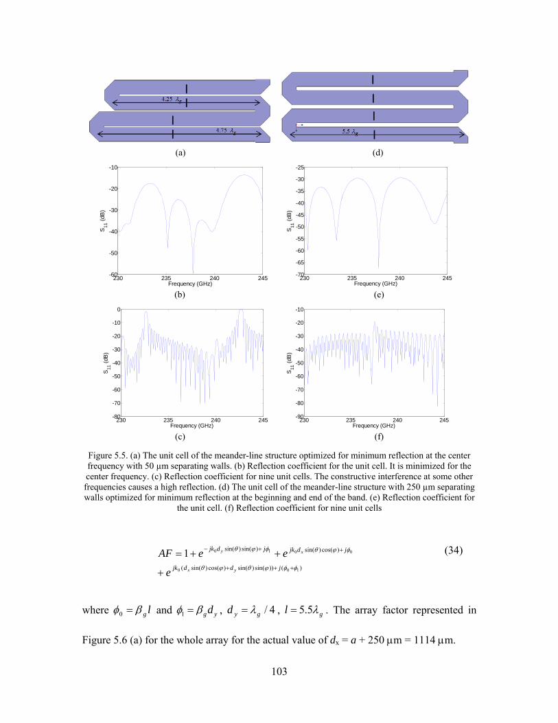
103
(a) (d)
230 235 240 245-60
-50
-40
-30
-20
-10
Frequency (GHz)
S1
1 (
dB)
230 235 240 245-70
-65
-60
-55
-50
-45
-40
-35
-30
-25
Frequency (GHz)S
11 (
dB)
(b) (e)
230 235 240 245-80
-70
-60
-50
-40
-30
-20
-10
0
Frequency (GHz)
S1
1 (
dB)
230 235 240 245-90
-80
-70
-60
-50
-40
-30
-20
-10
Frequency (GHz)
S1
1 (
dB)
(c) (f)
Figure 5.5. (a) The unit cell of the meander-line structure optimized for minimum reflection at the center frequency with 50 µm separating walls. (b) Reflection coefficient for the unit cell. It is minimized for the center frequency. (c) Reflection coefficient for nine unit cells. The constructive interference at some other frequencies causes a high reflection. (d) The unit cell of the meander-line structure with 250 µm separating walls optimized for minimum reflection at the beginning and end of the band. (e) Reflection coefficient for
the unit cell. (f) Reflection coefficient for nine unit cells
)())sin()sin()cos()sin((
)cos()sin()sin()sin(
100
00101
jddjk
jdjkjdjk
yx
xy
e
eeAF (34)
where lg 0 and ygd 1 , 4/gyd , gl 5.5 . The array factor represented in
Figure 5.6 (a) for the whole array for the actual value of dx = a + 250 m = 1114 m.

104
237.5 GHz
(a)
230 GHz 245 GHz
237.5 GHz
(b)
230 GHz 245 GHz
Figure 5.6. (a) Unit cell with reflection cancelling slot and the analytical far-field pattern of the array at the beginning, center and end of the band. (b).The final proposed structure with additional slot across the broad wall of the waveguide and the analytical far-field pattern of the array at the beginning, center and end of the band. It
is observable that the grating lobe is around -8 dB lower.
It is observable that the grating lobes are generated due to the fact that the spacing is
larger than half a free space wavelength ( 2.10 mm) which is mostly imposed by the
width of WR-3 waveguide. To overcome this problem, we assign two slots along the
width of the waveguide to make the spacing half as shown in Figure 5.6 (b). The array
factor of this structure can now be written as:
)())sin()sin()cos()sin(3()())sin()sin()cos()sin(2(
))sin()sin()cos()sin(()sin()sin()cos()sin(
100100
101001
jddjkjddjk
jddjkjdjkdjk
yxyx
yxyx
ee
eeeAF (35)
grating lobe
dy

105
As it is shown, the grating lobes have much lower amplitude (-8 dB lower) in the
azimuth direction and have been removed. This is mainly due to the fact that the antenna
physical size is increased which results in a narrower beam.
5.3. Conductor Loss
In a rectangular waveguide, the conductor loss is calculated from [71]
00
20
2
10
)2(
Zkab
akbkR
TE
cm
(36)
where
2
0mR , is the electrical conductivity, kc the cut-off frequency of the
waveguide, k0 wavenumber, Z0 free space characteristic impedance, a and b are width and
height of the waveguide. In 230~245 GHz band for the standard WR-3 waveguide size,
18 dB/m for gold and 16 dB/m for copper and the total loss for the meander-line
structure is around 6.6 dB for gold and 5.9 dB for copper which mean around 20% of the
power reaches the end of the waveguide. The amount of radiated power from slots should
be managed accordingly in order to have a uniform power distribution for each element.
5.4. Slot Positioning and Shape
Although transverse slots are not commonly used in array applications for broadside
radiation mainly because the spacing is twice as much the longitudinal slots which results
in grating lobes, they are successfully used in traveling-wave arrays for off-broadside

106
radiation [72] and are suitable for the application of this work since the length required to
generate the desired phase shift is provided by the length of the meander-line structure. In
addition, since these slots are used to excite patch arrays later and the patch arrays should
be oriented along the elevation direction, they should be positioned along the waveguide.
For the array positioned along the waveguide, transverse slots are the only options for
excitation.
230 240 250 260 270 280 290 300 310-0.6
-0.4
-0.2
0
0.2
0.4
0.6
0.8
1
1.2
Freq (GHz)
Zsl
ot/Z
0
RealImaginary
230 235 240 2450.8
1
1.2
1.4
1.6
1.8
2
2.2
2.4
2.6
2.8x 10⁻³
Freq (GHz)
radi
ated
pow
er %
w = 20 umw = 40 um
(a) (b)
Figure 5.7. (a) Normalized slot impedance versus frequency. A resonance happened at 282 GHz. (b) The total power associated with a non-resonant slot for two different widths.
At the resonant frequency, the amount of radiated power and thus the radiation
resistance of a slot are maximized as shown in Figure 5.7 (a). However, since in a large
array it is mostly desirable to distribute the power evenly among the elements, a small
amount of power is apportioned to each slot and thus the slots should be non-resonant. In
addition, the width of the waveguide does not allow two resonant ( 2/0 ) slots.
Therefore, the dimensions of the slots are chosen to be much smaller than 2/0 . By
changing the dimensions of the slots, we can control the amount of radiated power off
each slot. Figure 5.7 (b) shows the total power associated with a non-resonant slot
(radiated plus stored) for slots with around 4/0 length at two different widths. Since

107
the amount of propagating energy is decreased along the waveguide as it is partly
radiated and stored around each slot, and lost due to the finite conductivity of metal, the
dimensions of the slots should be increased gradually so that the radiated power remains
constant throughout the length of the waveguide even though the input power is
decreased. To design the slot dimensions, first we assume that the radiated power from
the four adjacent slots in each turn is constant. Therefore, considering the conductive
loss, in each turn
1112 4 PPPP cs (37)
where, P1 and P2 are the input and output powers in the waveguide, c is the percentage
of the conductive loss and s the percentage of the radiated power off of each slot. For
the next turn, the amount of the input power is decreased to P2 hence s for each slot
should be increased so that the total power sP remains constant. This recursive formula
is used to assign power for radiating slots in each turn considering the fact that only 20%
of the power is radiated. Ansoft HFSS is used to estimate the radiated power from slots
with different widths and the simulation results show that increasing the width of the slots
gradually from 5 m to 60 m guarantees uniform radiated power. The widths of each set
of the slots are shown in Figure 5.8
5 m 10 m 15 m 21 m 28 m 35 m 43 m 52 m 60 m
Figure 5.8. The slot width for each four turns so that nine different widths are used for the 36 turn waveguide. The length of the slots is 380 m.

108
5.5. Hybrid-Coupled Patch Array
As mentioned, the one-dimensional array of slots generates a very wide beam in the
elevation direction. For many applications ranging from collision avoidance to indoor
mapping, wide beamwidth is not desirable due to the possibility of the interference
caused by other targets. In order to confine the beam, we need to provide a long aperture
in that direction as well. One method to achieve this is to design patch arrays which are
fed by these slots. Figure 5.9 shows a hybrid-coupled patch array proposed to provide a
narrow beam in the elevation direction. In these arrays, the patches are positioned on top
of the slots separated by a dielectric substrate. The center patch is fed by the slot on the
bottom layer of the substrate, while the rest are series-fed through the center one [73].
The feeding is a combination of both planar and non-planar methods. The main
advantage of this coupling method is the ability to control the illumination function
separately in both array directions in order to produce a specified radiation pattern so that
while the pattern is scanning in the azimuth direction, it is fixed in the elevation direction.
Figure 5.9. Hybrid-coupled patch array fed by the main slot

109
However, the main issue associated with designing patch antennas at high frequencies
is that in order to suppress the propagation of the surface waves, very thin substrates are
required. For example, at 240 GHz, 50 m glass or 20 m silicon substrates are only
around one tenth of the guiding wavelength and they are almost impossible to handle. Yet
at the same time, they are thicker than what can be spun or deposited specifically for
most commonly used low-loss materials (such as spin-on glass [74] which can be spun up
to 5 m). In addition, dielectric materials add to the size and loss of the structure. Hence,
using a dielectric substrate for the patch array is not desired. Instead, an air substrate can
be used where the patch array is suspended on a thin layer of a thin dielectric membrane.
With an air substrate, no surface waves are excited, bandwidth is improved and the
efficiency is greatly enhanced.
In general, the design procedure can be organized in two parts: the series-fed patch
array and the aperture-coupled patch. The series-fed array consists of patches and high
impedance transmission lines. Quarter-wave transmission-line sections can be used to
minimize the return loss. To design a broadside standing wave patch array, all the patches
must be in phase so that both the patches and the connecting lines are approximated to be
half a guiding wavelength long. To obtain nearly uniform illumination for all the patches,
the widths are chosen to be identical. For maximum radiation, the patch width is
approximated as [75]
1
2
20
r
W
(38)
At 240 GHz for an air substrate W = 652 m. The width of the waveguide plus the

110
thickness of the separating walls ( 250 at m = 1114 m) should be able to
accommodate the width of two patch arrays (given that there are two slots along the
width). Since W > 1114 m / 2, we are required to decrease the width. This will also
increase the gap and help decrease the mutual coupling between the adjacent arrays. On
the other hand, wider patch provides narrower beamwidth in the azimuth direction which
helps lower the side lobe level. Therefore, an optimized width is required to provide a
narrow enough beamwidth in the azimuth direction with a minimized mutual coupling
A three-element series-fed patch array is designed with the help of the equivalent
circuit model of the patch antenna and shown in Figure 5.10 (a) and (b). The equivalent
conductance and susceptance of the patch antenna for 1.0/ 0 h are calculated as
2
00
)(24
11
120hk
WGr
)ln(636.01120 0
0
hkW
Br
(39)
(a)
(b)
Figure 5.10. (a) series-fed patch array, (b) equivalent circuit model of the series-fed patch array.

111
where h is the thickness of the substrate. This model is used to approximate the lengths of
patches and transmission lines which are slightly shorter than half a wavelength due the
presence of the slot admittance Gr+jBr. The end patch is slightly shorter than the other
patches in order to match the open-circuit end to the rest of the array. The final
optimization of the dimension is carried out by Ansoft HFSS to achieve the minimized
return loss at the center frequency.
As for the aperture-coupled (center) patch, the length of the patch and the connecting
transmission lines to the series-fed patch array are estimated using the circuit model
shown in Figure 5.11 (a) and then optimized by using Ansoft HFSS so that that the S-
parameters are resonant and the directivity of the antenna is maximized at the center
frequency as shown in Figure 5.11 (b). The radiation pattern of the hybrid-coupled patch
array for a total of seven elements (two three-element series fed each side of the center
patch) is presented in Figure 5.11 (c) and provides 80 of beamwidth.
To provide efficient slot-patch coupling, the thickness of the air substrate should be
kept below 100 m. For thicker substrates, the coupling is weakened as shown in Figure
5.12. As mentioned before, hollow structures including a patch substrate are fabricated
using silicon bulk micromachining. The proposed substrate will include patches and slots
on either side of the substrate which is a custom-made, non-standard ultra-thin wafer with
the precise thickness of the substrate. These substrates are costly and hard to handle. To
make the structure more robust for fabrication, the feasibility of using thick standard
substrate was investigated. As shown in Figure 5.13 incorporating dielectric walls
confine the field under the patch. The idea stems from the fact that the vertical field
component of the slot adjacent to the dielectric wall with a higher dielectric constant is
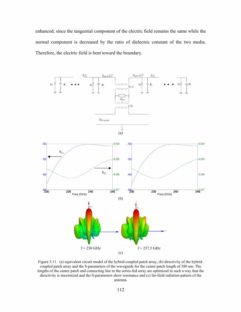
112
enhanced; since the tangential component of the electric field remains the same while the
normal component is decreased by the ratio of dielectric constant of the two media.
Therefore, the electric field is bent toward the boundary.
(a)
230 235 240 245-65
-60
-55
-50
Freq (GHz)230 235 240 245
-0.07
-0.06
-0.05
-0.04
(b)
f = 230 GHz f = 237.5 GHz
(c)
Figure 5.11. (a) equivalent circuit model of the hybrid-coupled patch array, (b) directivity of the hybrid-coupled patch array and the S-parameters of the waveguide for the center patch length of 380 um. The
lengths of the center patch and connecting line to the series-fed array are optimized in such a way that the directivity is maximized and the S-parameters show resonance and (c) far-field radiation pattern of the
antenna.
230 235 240 245-65
-60
-55
-50
Freq (GHz)230 235 240 245
-0.07
-0.06
-0.05
-0.04
S11
S21

113
(a) (b)
Figure 5.12. Electric field distribution for air substrate at 230 GHz (a) 80 um substrate (b) 250 um substrate (c) 250 um substrate with silicon walls
(a) (b) (c)
Figure 5.13. (a) Electric field at the boundary of two dielectric materials. The electric field distribution under a patch element excited from a very thin slot far from the patch element assisted by (b) high
dielectric vertical walls (c) dielectric block.
Although a single patch may now be excited on thick substrate, the rest of the array can
take advantage of a thin substrate as suggested by the structure shown in Figure 5.14 (a),
in which the center patch is fed through the slot with the thick air substrate and dielectric
block, while the rest of the patches are series-fed with the original thin substrate making a
multi-step structure. This structure can be fabricated on a thick standard wafer which is
more robust. The dimensions of the center patch and silicon block are optimized using
Ansoft HFSS. The simulation results show low side-lobe level and acceptable directivity
over the band shown in Figure 5.14. (b) and (c).
patch slot

114
(a)
(b) (c)
230 235 240 24516.9
17
17.1
17.2
17.3
17.4
17.5
17.6
17.7
17.8
Frequency (GHz)
Direct
ivity
(dB
)
(d)
Figure 5.14. (a) The proposed hybrid-coupled patch array with silicon block to enhance slot-patch coupling. (b) The electric field distribution (c) the radiation pattern at the center frequency 237.5 GHz and (d) the
directivity over the frequency band.
Figure 5.15. A developed version of hybrid-coupled patch array compatible with microfabrication.
lr
air gap
main slot reflection-cancelling slot
h1
h2
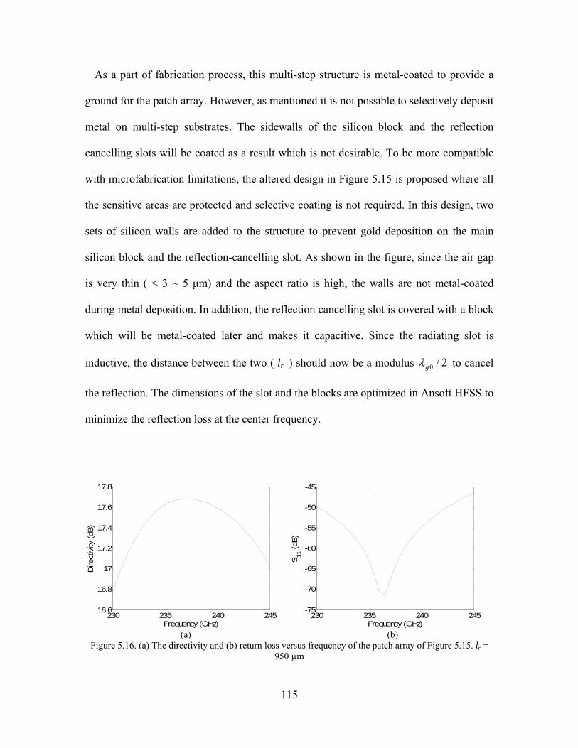
115
As a part of fabrication process, this multi-step structure is metal-coated to provide a
ground for the patch array. However, as mentioned it is not possible to selectively deposit
metal on multi-step substrates. The sidewalls of the silicon block and the reflection
cancelling slots will be coated as a result which is not desirable. To be more compatible
with microfabrication limitations, the altered design in Figure 5.15 is proposed where all
the sensitive areas are protected and selective coating is not required. In this design, two
sets of silicon walls are added to the structure to prevent gold deposition on the main
silicon block and the reflection-cancelling slot. As shown in the figure, since the air gap
is very thin ( < 3 ~ 5 μm) and the aspect ratio is high, the walls are not metal-coated
during metal deposition. In addition, the reflection cancelling slot is covered with a block
which will be metal-coated later and makes it capacitive. Since the radiating slot is
inductive, the distance between the two ( lr ) should now be a modulus 2/0g to cancel
the reflection. The dimensions of the slot and the blocks are optimized in Ansoft HFSS to
minimize the reflection loss at the center frequency.
230 235 240 24516.6
16.8
17
17.2
17.4
17.6
17.8
Frequency (GHz)
Dire
ctiv
ity (dB
)
230 235 240 245-75
-70
-65
-60
-55
-50
-45
Frequency (GHz)
S11 (dB
)
(a) (b)
Figure 5.16. (a) The directivity and (b) return loss versus frequency of the patch array of Figure 5.15. lr = 950 µm

116
5.6. The Final Design
The final antenna structure and its radiation pattern in the azimuth direction are shown
in Figure 5.17 (a) and (b). The presented results are from the analysis of half of the
structure with the current computer resources. It is noticeable that the main beam is
steering from -240 to +260 by changing the frequency from 230 GHz to 245 GHz. The
scan angle for different frequencies is listed in Table IX.
(a)
(b)
Figure 5.17. (a) The final structure (b) the radiation pattern in azimuth direction to verify the frequency scanning.
-50 0 50-30
-20
-10
0
10
20
30
X: -24Y: 26.73
Azimuth angle
Dire
ctiv
ity (dB
)
X: -8Y: 29.83
X: 8Y: 29.55 X: 26
Y: 26.12

117
Frequency (GHz) Scan Angle Directivity 230 -24 deg 26.73 dB 235 -8 deg 29.83
237.5 0 deg 29.87240 8 deg 29.55245 26 deg 26.12
Table IX. The scan angle and directivity versus frequency.
5.6.1. Sensitivity Analysis
Despite high level of accuracy, micromachining with multiple fabrication processes is
prone to errors caused by small misalignments, as well as geometrical distortions resulted
from lithography and etching. Etching silicon very deep (~432 µm) with uniformity and
high precision over large areas is rather difficult. The etch rate might vary depending on
the temperature, the position of the feature on the wafer, RIE lag effects, loading effects,
etc. One of the very common errors in DRIE etching is the non-uniformity in large open
areas. Basically, the edges of the wafer are etched faster than the center resulting in
bowed surface structure as shown in Figure (a). This effect could be further increased in
structure such as meander-line waveguide due to the loading effect cause by the adjacent
channels. The non-uniformity in not trivial and can be up to 15%. However, since it only
affects the height of the waveguide, it does not change the propagation constant and
dispersion characteristics of TE10 mode of the waveguide which is only the function of
waveguide width. However, for a reduced-height waveguide, loss increases as shown in
Figure (b). It is noticeable that 70 µm error in height causes around 10% increase in
waveguide loss.
In addition, since the etched area for the meander-line structure is very long (~ 36 cm)
and multi-step patterning and etching are required for this large area, a spotless pattering
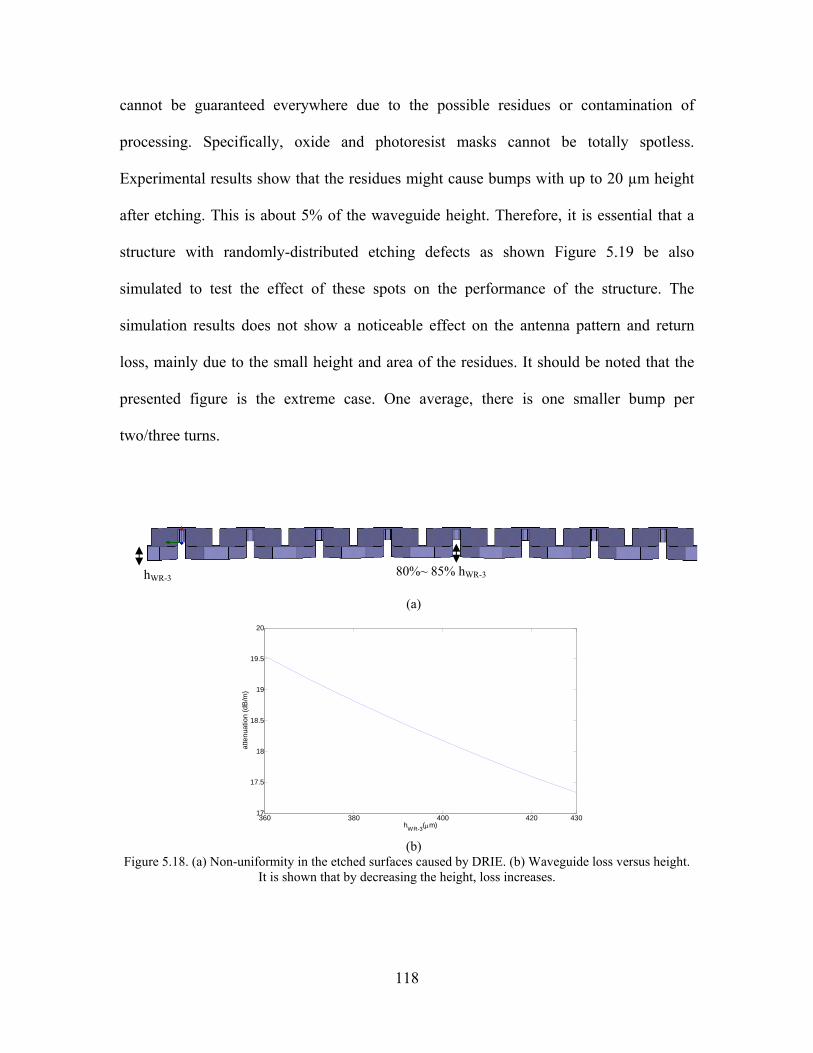
118
cannot be guaranteed everywhere due to the possible residues or contamination of
processing. Specifically, oxide and photoresist masks cannot be totally spotless.
Experimental results show that the residues might cause bumps with up to 20 µm height
after etching. This is about 5% of the waveguide height. Therefore, it is essential that a
structure with randomly-distributed etching defects as shown Figure 5.19 be also
simulated to test the effect of these spots on the performance of the structure. The
simulation results does not show a noticeable effect on the antenna pattern and return
loss, mainly due to the small height and area of the residues. It should be noted that the
presented figure is the extreme case. One average, there is one smaller bump per
two/three turns.
(a)
360 380 400 420 43017
17.5
18
18.5
19
19.5
20
hWR-3
(m)
atte
nua
tion
(d
B/m
)
(b)
Figure 5.18. (a) Non-uniformity in the etched surfaces caused by DRIE. (b) Waveguide loss versus height. It is shown that by decreasing the height, loss increases.
hWR-3 80%~ 85% hWR-3

119
Figure 5.19. Two cells of the antenna structure are simulated with randomly-distributed defects with 20 µm height and 50 µm × 100 µm area (corresponding to the largest bump experimentally measured)
5.7. Modified Design for Reduced Loss
As shown in section 5.3, the conductor loss for WR-3 standard waveguide is around 18
dB/m and therefore causes around 7 dB loss in the antenna structure which above 80 % of
the power. This fact requires us to design very narrow slots (as narrow as 5 μm) in order
to distribute the power evenly among all the elements. This has two drawbacks: first,
80% power loss makes the antenna very inefficient and second, an extremely highly
sensitive system is required to measure the radiated power off of the tiny slots.
In general, standard waveguides are designed for 2:1 operation bandwidth and that
justifies the 2:1 ratio of the width to the height. The dimensions are determined based on
limited dispersion and evanescent-wave coupling of the higher order modes throughout
the whole band (which is 220 – 325 GHz for the WR-3 waveguide). However, loss is not
necessarily optimized. As we use a very small fraction of the band, the loss of the
waveguide can be optimized considering all the above facts and microfabrication
limitations.
Figure 5.20 shows the waveguide conductor loss for different widths and heights at the
end of the band. As expected, it is observable that loss is decreased as the dimensions are

120
increased. Based on limitations on microfabrication, antenna design and the possibility of
the excitation of higher order modes, very wide and deep waveguides cannot be chosen.
With some intermediated dimensions such as a = 1100 μm and b = 700 μm the
waveguide loss is reduced to half while many of the other design parameters can be
maintained.
300 350 400 450 500 550 600 650 700 750 800-22
-20
-18
-16
-14
-12
-10
-8X: 700Y: -10.65
Waveguide Height (m)
Att
enua
tion
(dB
/m)
0.8 1 1.2 1.4 1.6 1.8 2-20
-18
-16
-14
-12
-10
-8
-6
Waveguide Width (mm)
Att
enua
tion
(dB
/m)
X: 1.1Y: -10.65
(a) (b)
Figure 5.20. Waveguide loss (a) versus waveguide height for width = 1100 μm (b) versus waveguide width for height = 700 μm
230 235 240 2453000
3200
3400
3600
3800
4000
4200
4400
Frequency (GHz)
reduced-loss waveguideWR-3 standard waveguide
y/x=25.6
y/x=30.75
Figure 5.21. The dispersion diagram: propagation constant (β) versus frequency. The slope is decreased for the reduced-loss waveguide

121
However, the dispersion characteristics of such a waveguide are slightly different from
the WR-3 standard waveguide. As shown in the dispersion diagram of Figure 5.21, the
slope of propagation constant is lower and thus the longer waveguide length are required
to provide the desired phase shift. For ±250 scan range, l is chosen to be 8.5 0g = 1.3 cm.
In order to further reduce the loss, waveguide length is decreased to around 3 cm so that
the number of radiating element is decreased and the amount of power assigned to the
slots can be increased. It is noticeable that 0.5 cm reduction in waveguide length
increased the beamwidth by only 0.50 and the design beamwidth is now 2.50.
Now that the overall waveguide loss has decreased, more power can be assigned to
each slot. As will be shown later, the low input power and dynamic range of the system
limit the capability to measure the radiated power off the narrow slots. Therefore, in this
design the dimensions of the slots have increased as well as shown in Figure 5.22 . Also,
the reflection cancelling slots are eliminated since as the slots are non-resonant, the
reflection from each is a very trivial amount. Therefore, most of the power is now
assigned to the radiating slots.
60 m 70 m 80 m 100 m 120 140 160 200 200 200 200
Figure 5.22. The slot width for each four/two turns so that eight different widths are used for the 28 turn waveguide. The length of the slots is 400 m.

122
5.8. Conclusion
In this chapter, the design details of MMW frequency scanning antenna were discussed.
The design of meander-line waveguide for minimized reflection, slots dimensions and
orientation and hybrid-coupled patch array were studied. The chapter finishes with a
modified design with lower overall conductor loss and higher efficiency.
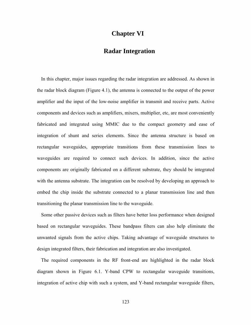
123
Chapter VI
6. Radar Integration
In this chapter, major issues regarding the radar integration are addressed. As shown in
the radar block diagram (Figure 4.1), the antenna is connected to the output of the power
amplifier and the input of the low-noise amplifier in transmit and receive parts. Active
components and devices such as amplifiers, mixers, multiplier, etc, are most conveniently
fabricated and integrated using MMIC due to the compact geometry and ease of
integration of shunt and series elements. Since the antenna structure is based on
rectangular waveguides, appropriate transitions from these transmission lines to
waveguides are required to connect such devices. In addition, since the active
components are originally fabricated on a different substrate, they should be integrated
with the antenna substrate. The integration can be resolved by developing an approach to
embed the chip inside the substrate connected to a planar transmission line and then
transitioning the planar transmission line to the waveguide.
Some other passive devices such as filters have better loss performance when designed
based on rectangular waveguides. These bandpass filters can also help eliminate the
unwanted signals from the active chips. Taking advantage of waveguide structures to
design integrated filters, their fabrication and integration are also investigated.
The required components in the RF front-end are highlighted in the radar block
diagram shown in Figure 6.1. Y-band CPW to rectangular waveguide transitions,
integration of active chip with such a system, and Y-band rectangular waveguide filters,

124
all compatible with micromachining methods are studied and novel approaches are
proposed and verified.
Figure 6.1. The passive components for radar integration are highlighted in the radar block diagram. These
components include CPW/waveguide transition, bandpass waveguide filters and active chip packaging.
6.1. CBCPW to Rectangular Waveguide Transition
Traditional CPW to rectangular waveguide transitions based on E-plane probe
excitation involve attaching a suspended resonant probe to the center conductor of a
CPW lines from broad wall of the waveguide ([76], [77]) as shown in Figure 6.2 (a). This
transition covers the waveguide band and is easy to fabricate at microwave and low
MMW frequencies using the standard fabrication and assembly methods. At high MMW
and SMMW frequencies fabrication of very small suspended probe within a waveguide
with micromachining techniques becomes challenging. In [78] - [80], using non-contact
lithography, the CPW line is patterned after etching the suspended probe. However, since
photoresist cannot be spun uniformly in the presence of the probe and the wafer and the

125
mask cannot be in contact during lithography, the quality of patterning deteriorates.
Alternatively, if the CPW is patterned first, the surface cannot be etched to form the
probe. Attaching a suspended probe to wafer eventually is not practical, either.
The microfabrication of a transition can be performed conveniently using two stacked
wafers, if a short-circuited probe extending the entire height of the waveguide can be
used. The waveguide trench and the probe are patterned and etched on one substrate
while the CPW line is patterned on another substrate which is bonded to the trench later
to form a waveguide as shown in Figure 6.2 (b). Nonetheless, a short-circuited probe acts
purely reactive and cannot be matched to the CPW line. To properly excite a waveguide
with this probe, a resonant condition must be achieved to eliminate the probe reactance. It
is well-known that a pin terminated by the broad wall of a rectangular waveguide acts as
an inductive element whose inductance is inversely proportional to its diameter and the
waveguide dimensions [81]. The geometry and the equivalent circuit model of a shorting
pin are shown in Figure 6.3 (a). For this case the transformer turn ratio can be calculated
from [82]
2tan2
ka
ka
b
an
(40)
where, a and b are the width and height of the rectangular waveguide and k is the free
space wavenumber. To compensate for the inductance of the shorting pin Xp, a capacitive
element is needed. Since a step discontinuity in the E-plane of the waveguide acts as a
capacitive element, it can compensate for the inductive behavior of the pin.
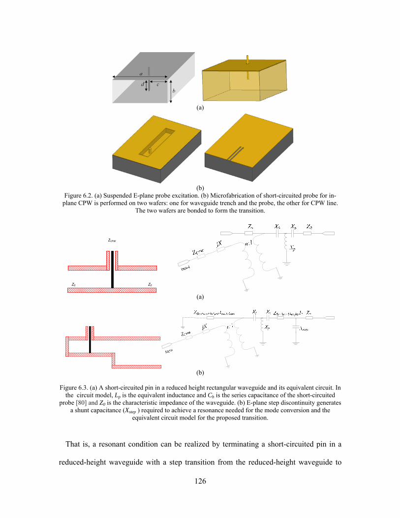
126
(a)
(b)
Figure 6.2. (a) Suspended E-plane probe excitation. (b) Microfabrication of short-circuited probe for in-plane CPW is performed on two wafers: one for waveguide trench and the probe, the other for CPW line.
The two wafers are bonded to form the transition.
ZCPW
Z0 Z0
(a)
(b)
Figure 6.3. (a) A short-circuited pin in a reduced height rectangular waveguide and its equivalent circuit. In
the circuit model, Lp is the equivalent inductance and Cb is the series capacitance of the short-circuited probe [80] and Z0 is the characteristic impedance of the waveguide. (b) E-plane step discontinuity generates
a shunt capacitance (Xstep ) required to achieve a resonance needed for the mode conversion and the equivalent circuit model for the proposed transition.
That is, a resonant condition can be realized by terminating a short-circuited pin in a
reduced-height waveguide with a step transition from the reduced-height waveguide to
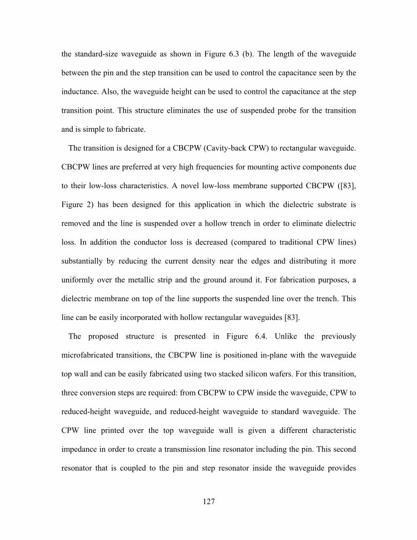
127
the standard-size waveguide as shown in Figure 6.3 (b). The length of the waveguide
between the pin and the step transition can be used to control the capacitance seen by the
inductance. Also, the waveguide height can be used to control the capacitance at the step
transition point. This structure eliminates the use of suspended probe for the transition
and is simple to fabricate.
The transition is designed for a CBCPW (Cavity-back CPW) to rectangular waveguide.
CBCPW lines are preferred at very high frequencies for mounting active components due
to their low-loss characteristics. A novel low-loss membrane supported CBCPW ([83],
Figure 2) has been designed for this application in which the dielectric substrate is
removed and the line is suspended over a hollow trench in order to eliminate dielectric
loss. In addition the conductor loss is decreased (compared to traditional CPW lines)
substantially by reducing the current density near the edges and distributing it more
uniformly over the metallic strip and the ground around it. For fabrication purposes, a
dielectric membrane on top of the line supports the suspended line over the trench. This
line can be easily incorporated with hollow rectangular waveguides [83].
The proposed structure is presented in Figure 6.4. Unlike the previously
microfabricated transitions, the CBCPW line is positioned in-plane with the waveguide
top wall and can be easily fabricated using two stacked silicon wafers. For this transition,
three conversion steps are required: from CBCPW to CPW inside the waveguide, CPW to
reduced-height waveguide, and reduced-height waveguide to standard waveguide. The
CPW line printed over the top waveguide wall is given a different characteristic
impedance in order to create a transmission line resonator including the pin. This second
resonator that is coupled to the pin and step resonator inside the waveguide provides

128
another impedance match. The center conductor of the CPW line is open-circuited at the
location of the pin and the pin is connected to the lower wall of a reduced-height
waveguide. On the other side of the pin, the reduced-height waveguide is short-circuited
at a distance to appear as another reactance parallel to the pin inductance. The
discontinuity from CBCPW line to CPW line inside the waveguide is also modeled by a
shunt capacitance. To design the transition, first the dimensions of waveguide and
CBCPW line are chosen based on the desired frequency range. The initial values of
elements of the circuit model are selected using the analytical formulas and measurement
results reported in [81] and [82]. These values along with the length of waveguide and
CPW line sections are optimized using transmission line analysis of the circuit model to
obtain the resonant behavior. A structure based on these values is designed and then
optimized using the full-wave simulator Ansoft HFSS.
Figure 6.4. CBCPW to rectangular waveguide transition, top view, side view and the perspective of a back-to-back configuration which includes a transition from CBCPW to CPW, CPW to reduced-height
waveguide and reduced-height waveguide to the standardWR-3 rectangular waveguide.

129
To verify the performance, two sets of transitions for different frequency ranges were
designed and fabricated: one at the lower MMW band (Ka-band) with standard
machining techniques and another at our desired frequency band (240 GHz).
6.1.1. Ka-band Transition
A prototype at Ka-band for WR-28 waveguides was designed and the reflection
coefficient of the optimized structure is compared to that of the circuit model for the
back-to-back transition in Figure 6.5 to verify the performance of the transition. As
shown, a good agreement is obtained while the physical structure provides a better
performance than the one predicted by the circuit model. The electric field distribution of
the optimized structure is shown in Figure 6.6 (a) and well represents the conversion of
the CPW mode to the waveguide mode using the terminated pin. Figure 6.6 (b) shows the
reflection and transmission coefficients of this transition. It is observed that a
transmission above -1 dB and reflection below -10 dB for more than 9% of the bandwidth
can be achieved. An enlarged plot of the transmission coefficient over the passband is
also shown in Figure 6.6 (c).
The bandwidth of the transition is sufficient for most application at these very high
frequencies. However, in situations where more bandwidth is needed, the number of
shorting pins and step discontinuities can be increased accordingly. To add one more
resonance, another shorting pin and step discontinuity can be introduced. The geometry
of a three-pole structure is shown in Figure 6.7 (a). The simulated transition and
reflection coefficients of the structure are presented in Figure 6.7 (b). It is shown that the
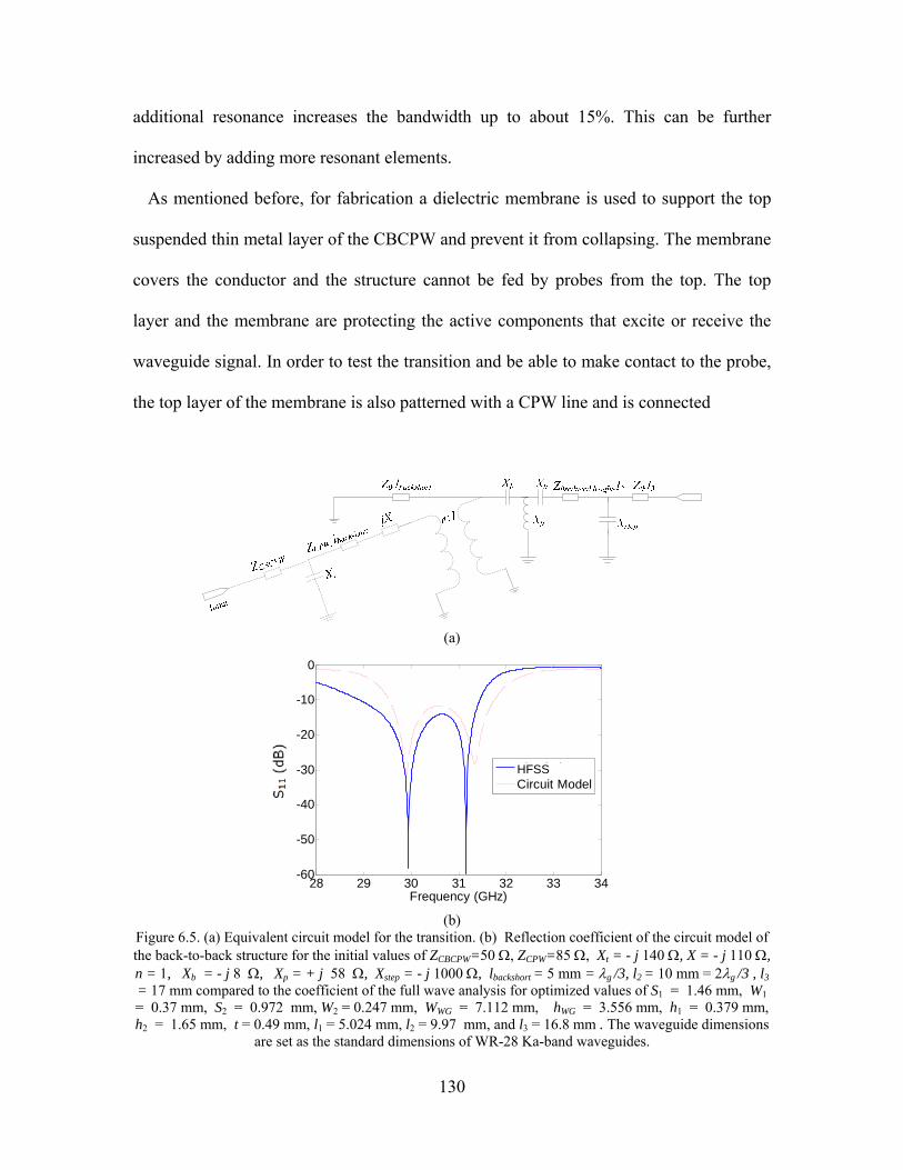
130
additional resonance increases the bandwidth up to about 15%. This can be further
increased by adding more resonant elements.
As mentioned before, for fabrication a dielectric membrane is used to support the top
suspended thin metal layer of the CBCPW and prevent it from collapsing. The membrane
covers the conductor and the structure cannot be fed by probes from the top. The top
layer and the membrane are protecting the active components that excite or receive the
waveguide signal. In order to test the transition and be able to make contact to the probe,
the top layer of the membrane is also patterned with a CPW line and is connected
(a)
28 29 30 31 32 33 34-60
-50
-40
-30
-20
-10
0
Frequency (GHz)
dB (
S11
)
SimulationCircuit ModelHFSS
(b)
Figure 6.5. (a) Equivalent circuit model for the transition. (b) Reflection coefficient of the circuit model of the back-to-back structure for the initial values of ZCBCPW=50 , ZCPW=85 , Xt = - j 140 , X = - j 110 , n = 1, Xb = - j 8 , Xp = + j 58 , Xstep = - j 1000 , lbackshort = 5 mm = g /3, l2 = 10 mm = 2g /3 , l3
= 17 mm compared to the coefficient of the full wave analysis for optimized values of S1 = 1.46 mm, W1 = 0.37 mm, S2 = 0.972 mm, W2 = 0.247 mm, WWG = 7.112 mm, hWG = 3.556 mm, h1 = 0.379 mm, h2 = 1.65 mm, t = 0.49 mm, l1 = 5.024 mm, l2 = 9.97 mm, and l3 = 16.8 mm . The waveguide dimensions
are set as the standard dimensions of WR-28 Ka-band waveguides.
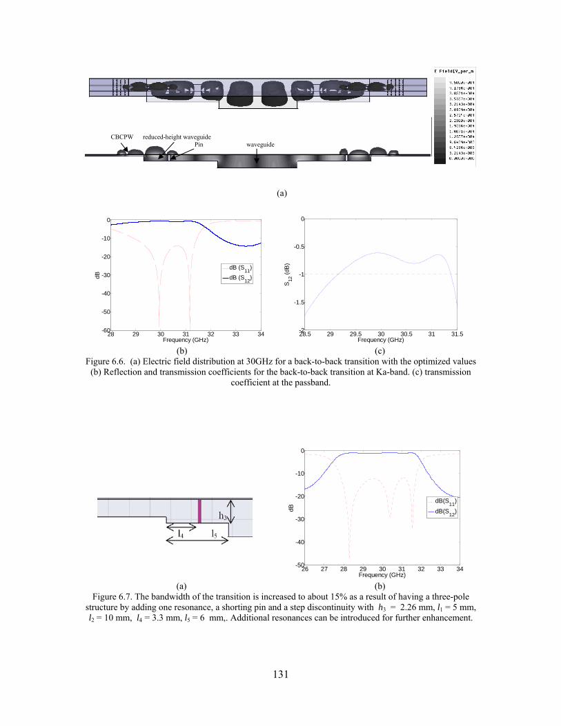
131
(a)
28 29 30 31 32 33 34-60
-50
-40
-30
-20
-10
0
Frequency (GHz)
dB
dB (S11
)
dB (S12
)
28.5 29 29.5 30 30.5 31 31.5-2
-1.5
-1
-0.5
0
Frequency (GHz)
S12
(dB
)
(b) (c)
Figure 6.6. (a) Electric field distribution at 30GHz for a back-to-back transition with the optimized values (b) Reflection and transmission coefficients for the back-to-back transition at Ka-band. (c) transmission
coefficient at the passband.
26 27 28 29 30 31 32 33 34-50
-40
-30
-20
-10
0
Frequency (GHz)
dB
dB(S11
)
dB(S12
)
(a) (b) Figure 6.7. The bandwidth of the transition is increased to about 15% as a result of having a three-pole
structure by adding one resonance, a shorting pin and a step discontinuity with h3 = 2.26 mm, l1 = 5 mm, l2 = 10 mm, l4 = 3.3 mm, l5 = 6 mm,. Additional resonances can be introduced for further enhancement.
CBCPW reduced-height waveguide Pin waveguide
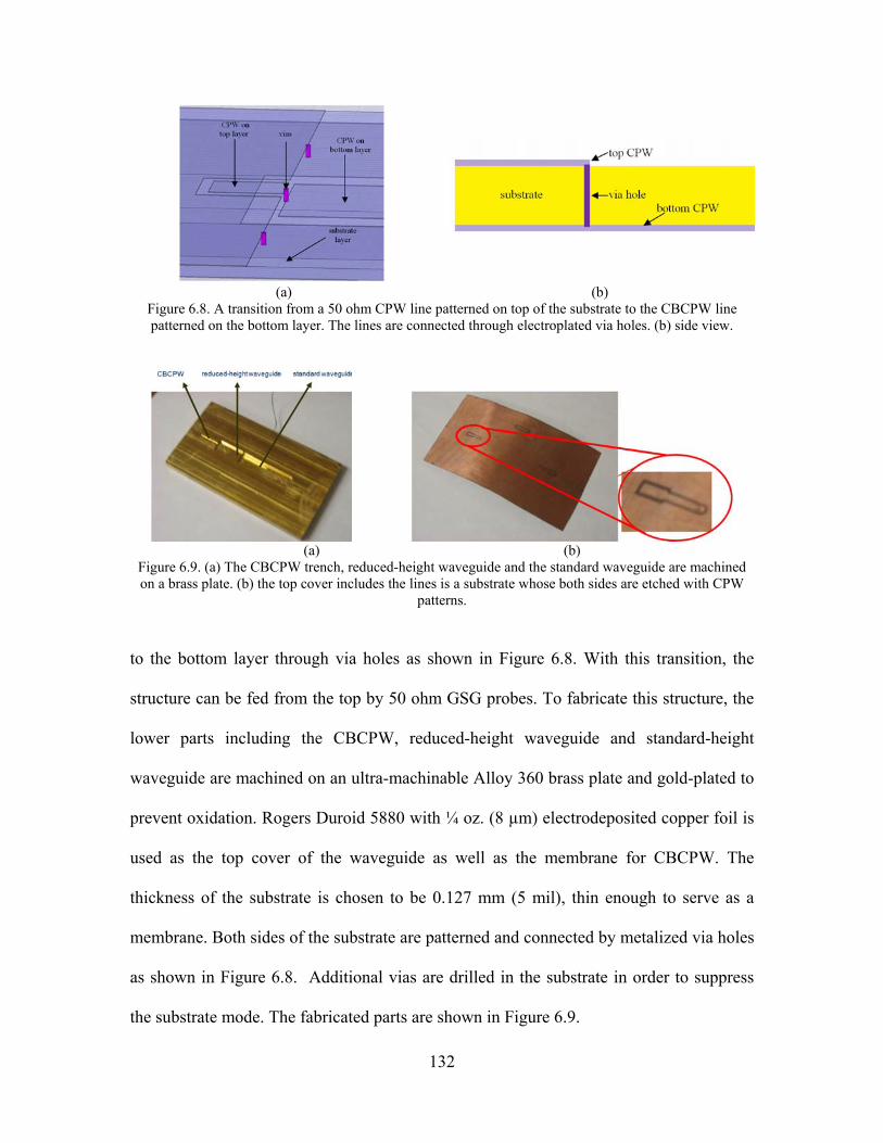
132
(a) (b) Figure 6.8. A transition from a 50 ohm CPW line patterned on top of the substrate to the CBCPW line patterned on the bottom layer. The lines are connected through electroplated via holes. (b) side view.
(a) (b)
Figure 6.9. (a) The CBCPW trench, reduced-height waveguide and the standard waveguide are machined on a brass plate. (b) the top cover includes the lines is a substrate whose both sides are etched with CPW
patterns.
to the bottom layer through via holes as shown in Figure 6.8. With this transition, the
structure can be fed from the top by 50 ohm GSG probes. To fabricate this structure, the
lower parts including the CBCPW, reduced-height waveguide and standard-height
waveguide are machined on an ultra-machinable Alloy 360 brass plate and gold-plated to
prevent oxidation. Rogers Duroid 5880 with ¼ oz. (8 µm) electrodeposited copper foil is
used as the top cover of the waveguide as well as the membrane for CBCPW. The
thickness of the substrate is chosen to be 0.127 mm (5 mil), thin enough to serve as a
membrane. Both sides of the substrate are patterned and connected by metalized via holes
as shown in Figure 6.8. Additional vias are drilled in the substrate in order to suppress
the substrate mode. The fabricated parts are shown in Figure 6.9.
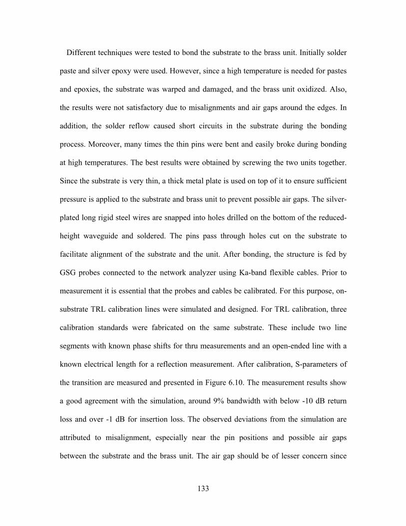
133
Different techniques were tested to bond the substrate to the brass unit. Initially solder
paste and silver epoxy were used. However, since a high temperature is needed for pastes
and epoxies, the substrate was warped and damaged, and the brass unit oxidized. Also,
the results were not satisfactory due to misalignments and air gaps around the edges. In
addition, the solder reflow caused short circuits in the substrate during the bonding
process. Moreover, many times the thin pins were bent and easily broke during bonding
at high temperatures. The best results were obtained by screwing the two units together.
Since the substrate is very thin, a thick metal plate is used on top of it to ensure sufficient
pressure is applied to the substrate and brass unit to prevent possible air gaps. The silver-
plated long rigid steel wires are snapped into holes drilled on the bottom of the reduced-
height waveguide and soldered. The pins pass through holes cut on the substrate to
facilitate alignment of the substrate and the unit. After bonding, the structure is fed by
GSG probes connected to the network analyzer using Ka-band flexible cables. Prior to
measurement it is essential that the probes and cables be calibrated. For this purpose, on-
substrate TRL calibration lines were simulated and designed. For TRL calibration, three
calibration standards were fabricated on the same substrate. These include two line
segments with known phase shifts for thru measurements and an open-ended line with a
known electrical length for a reflection measurement. After calibration, S-parameters of
the transition are measured and presented in Figure 6.10. The measurement results show
a good agreement with the simulation, around 9% bandwidth with below -10 dB return
loss and over -1 dB for insertion loss. The observed deviations from the simulation are
attributed to misalignment, especially near the pin positions and possible air gaps
between the substrate and the brass unit. The air gap should be of lesser concern since
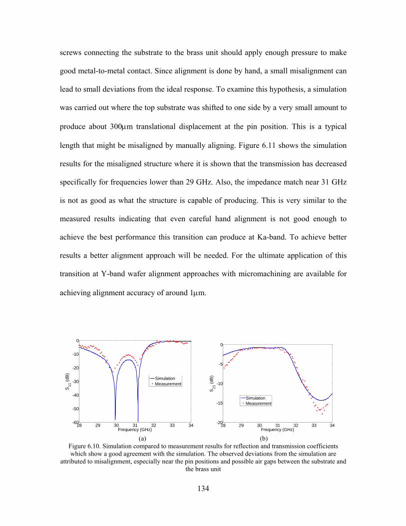
134
screws connecting the substrate to the brass unit should apply enough pressure to make
good metal-to-metal contact. Since alignment is done by hand, a small misalignment can
lead to small deviations from the ideal response. To examine this hypothesis, a simulation
was carried out where the top substrate was shifted to one side by a very small amount to
produce about 300m translational displacement at the pin position. This is a typical
length that might be misaligned by manually aligning. Figure 6.11 shows the simulation
results for the misaligned structure where it is shown that the transmission has decreased
specifically for frequencies lower than 29 GHz. Also, the impedance match near 31 GHz
is not as good as what the structure is capable of producing. This is very similar to the
measured results indicating that even careful hand alignment is not good enough to
achieve the best performance this transition can produce at Ka-band. To achieve better
results a better alignment approach will be needed. For the ultimate application of this
transition at Y-band wafer alignment approaches with micromachining are available for
achieving alignment accuracy of around 1m.
28 29 30 31 32 33 34-60
-50
-40
-30
-20
-10
0
Frequency (GHz)
S1
1 (
dB)
SimulationMeasurement
28 29 30 31 32 33 34-20
-15
-10
-5
0
Frequency (GHz)
S2
1 (
dB)
SimulationMeasurement
(a) (b)
Figure 6.10. Simulation compared to measurement results for reflection and transmission coefficients which show a good agreement with the simulation. The observed deviations from the simulation are
attributed to misalignment, especially near the pin positions and possible air gaps between the substrate and the brass unit
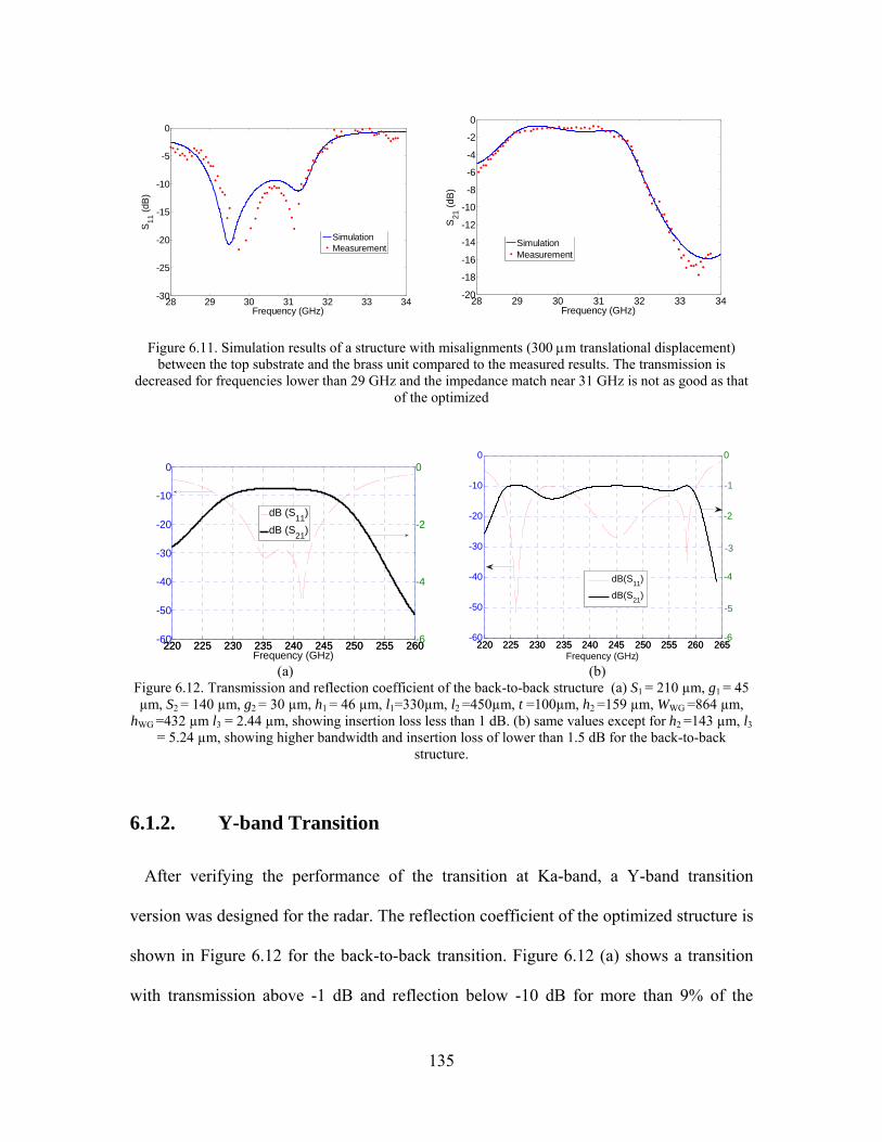
135
28 29 30 31 32 33 34-30
-25
-20
-15
-10
-5
0
Frequency (GHz)
S1
1 (dB
)
SimulationMeasurement
28 29 30 31 32 33 34-20
-18
-16
-14
-12
-10
-8
-6
-4
-2
0
Frequency (GHz)
S21
(dB
)
SimulationMeasurement
Figure 6.11. Simulation results of a structure with misalignments (300 m translational displacement) between the top substrate and the brass unit compared to the measured results. The transmission is
decreased for frequencies lower than 29 GHz and the impedance match near 31 GHz is not as good as that of the optimized
220 225 230 235 240 245 250 255 260-60
-50
-40
-30
-20
-10
0
Frequency (GHz)
220 225 230 235 240 245 250 255 260-6
-4
-2
0
dB (S11
)
dB (S21
)
220 225 230 235 240 245 250 255 260 265-60
-50
-40
-30
-20
-10
0
Frequency (GHz)
220 225 230 235 240 245 250 255 260 265-6
-4
-2
0
dB(S11
)
dB(S21
)
-1
-3
-5
(a) (b)
Figure 6.12. Transmission and reflection coefficient of the back-to-back structure (a) S1 = 210 µm, g1 = 45 µm, S2 = 140 µm, g2 = 30 µm, h1 = 46 µm, l1=330µm, l2 =450µm, t =100µm, h2 =159 µm, WWG =864 µm,
hWG =432 µm l3 = 2.44 µm, showing insertion loss less than 1 dB. (b) same values except for h2 =143 µm, l3 = 5.24 µm, showing higher bandwidth and insertion loss of lower than 1.5 dB for the back-to-back
structure.
6.1.2. Y-band Transition
After verifying the performance of the transition at Ka-band, a Y-band transition
version was designed for the radar. The reflection coefficient of the optimized structure is
shown in Figure 6.12 for the back-to-back transition. Figure 6.12 (a) shows a transition
with transmission above -1 dB and reflection below -10 dB for more than 9% of the
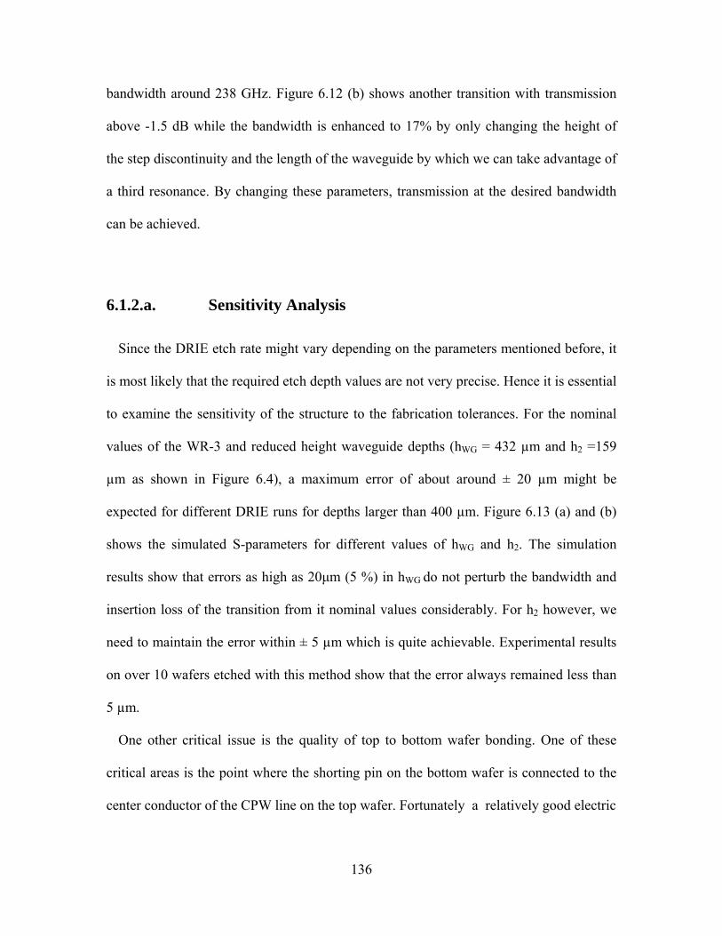
136
bandwidth around 238 GHz. Figure 6.12 (b) shows another transition with transmission
above -1.5 dB while the bandwidth is enhanced to 17% by only changing the height of
the step discontinuity and the length of the waveguide by which we can take advantage of
a third resonance. By changing these parameters, transmission at the desired bandwidth
can be achieved.
6.1.2.a. Sensitivity Analysis
Since the DRIE etch rate might vary depending on the parameters mentioned before, it
is most likely that the required etch depth values are not very precise. Hence it is essential
to examine the sensitivity of the structure to the fabrication tolerances. For the nominal
values of the WR-3 and reduced height waveguide depths (hWG = 432 µm and h2 =159
µm as shown in Figure 6.4), a maximum error of about around ± 20 µm might be
expected for different DRIE runs for depths larger than 400 µm. Figure 6. 13 (a) and (b)
shows the simulated S-parameters for different values of hWG and h2. The simulation
results show that errors as high as 20μm (5 %) in hWG do not perturb the bandwidth and
insertion loss of the transition from it nominal values considerably. For h2 however, we
need to maintain the error within ± 5 µm which is quite achievable. Experimental results
on over 10 wafers etched with this method show that the error always remained less than
5 µm.
One other critical issue is the quality of top to bottom wafer bonding. One of these
critical areas is the point where the shorting pin on the bottom wafer is connected to the
center conductor of the CPW line on the top wafer. Fortunately a relatively good electric

137
contact can be established between the pin and the CPW center conductors. This is
verified by measuring the ohmic resistance between signal and ground. To investigate
performance degradation in case of weak gold bonding over the pin, simulations are
carried out allowing a small gap between the pin and the center conductor. Figure 6. 13
(c) and (d) represents how much the transmission and reflection coefficients are affected
in case the pin is not electrically connected to the top wafer. The results show that a gap
size values below 3 µm, does not affect the S-parameters significantly. For the actual
structure, since the membrane does not have a large stress and does not buckle, a gap
larger than a micron is not expected.
220 235 250 265-7
-5
-3
-1
0
Frequency (GHz)
S21
(dB
)
h= - 20m
h= +20m
h= 0
220 235 250 265-5
-3
-1-0.5
Frequency (GHz)
S21
(dB
)
h=5 m
h=10 m
h=15 m
h=20 m
(a) (b)
225 245 265-60
-40
-20
0
Frequency (GHz)
S21
(dB
)
gap size
10 m
0 m
225 245 265
-5.5
-3.5
-1.5
Frequency (GHz)
S11
(dB
)
0 m
10 m
6 mgap size
(c) (d)
Figure 6. 13. Transmission coefficient of the transition when (a) hWG is varied ± 20 µm (~5%) showing the response of the transition is insensitive to variations in waveguide height, b) the response is shown to be
more sensitive to the reduced waveguide height h2 for h > 5 µm . (c) The transmission and (d) the reflection coefficients when a gap is assigned between the top of the pin on the bottom wafer and the top
wafer. The response degrades for gaps above 3 µm.
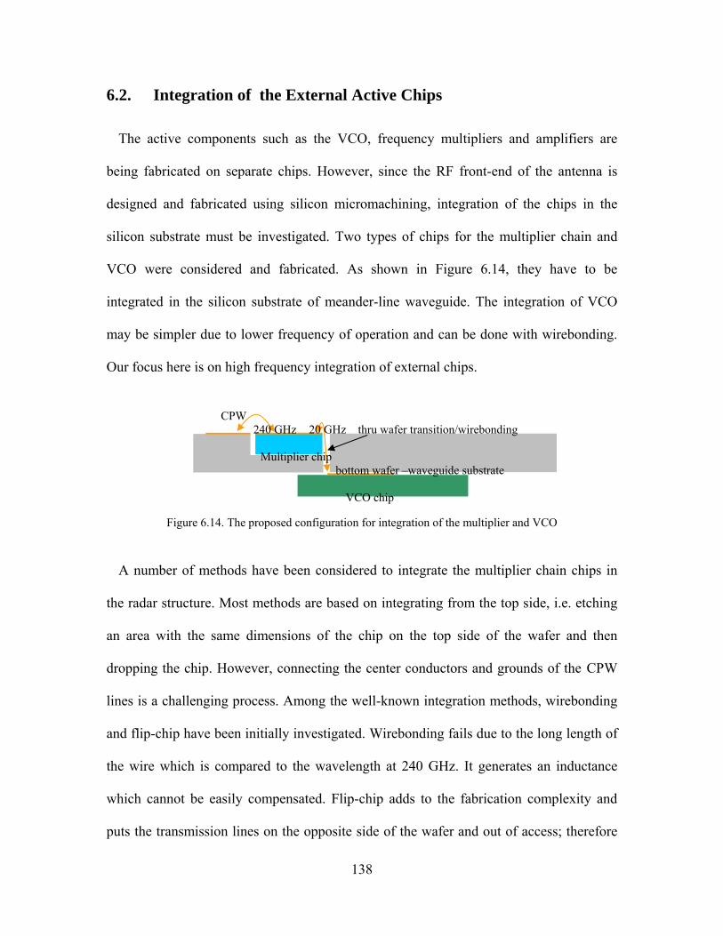
138
6.2. Integration of the External Active Chips
The active components such as the VCO, frequency multipliers and amplifiers are
being fabricated on separate chips. However, since the RF front-end of the antenna is
designed and fabricated using silicon micromachining, integration of the chips in the
silicon substrate must be investigated. Two types of chips for the multiplier chain and
VCO were considered and fabricated. As shown in Figure 6. 14, they have to be
integrated in the silicon substrate of meander-line waveguide. The integration of VCO
may be simpler due to lower frequency of operation and can be done with wirebonding.
Our focus here is on high frequency integration of external chips.
Figure 6. 14. The proposed configuration for integration of the multiplier and VCO
A number of methods have been considered to integrate the multiplier chain chips in
the radar structure. Most methods are based on integrating from the top side, i.e. etching
an area with the same dimensions of the chip on the top side of the wafer and then
dropping the chip. However, connecting the center conductors and grounds of the CPW
lines is a challenging process. Among the well-known integration methods, wirebonding
and flip-chip have been initially investigated. Wirebonding fails due to the long length of
the wire which is compared to the wavelength at 240 GHz. It generates an inductance
which cannot be easily compensated. Flip-chip adds to the fabrication complexity and
puts the transmission lines on the opposite side of the wafer and out of access; therefore
CPW 240 GHz 20 GHz thru wafer transition/wirebonding
Multiplier chip bottom wafer –waveguide substrate
VCO chip

139
direct DC connection for bias with wireboding is not possible. In addition, in both
methods the high temperature and pressure of bonding will damage the electronic
components.
A method based on capacitive coupling that provides access to the DC lines and
requires the external chip to be embedded after the bonding, was developed and is shown
in Figure 6. 15. In this design, the area required for the chip is etched all the way through
the substrate to make a hole. This allows the chip to be inserted from the backside of the
substrate in the final stage of the fabrication. Figure 6. 16 shows the structure of the thru-
wafer transition for packaging. The chip has to be connected to the CBCPW line on the
wafer (which is connected to the rectangular waveguide using the aforementioned
transition). Since the width of the CBCPW is quite different from those of grounded
CPW on the chip, the CPCPW is connected to a /2 line with a narrower center
conductor with similar dimensions of the chip center conductor and gap to smoothen the
transition. The characteristic impedance of this line is not 50 ohm, but it is not critical
since the length is /2. The line is extended on top of the chip to cover the CPW part and
if the chip is well-inserted, creates a connection between the line and the chip. However,
the chip might have gaps from the sides and the top in case the pressure is not enough or
the surfaces are not uniform and flat. The transition is optimized for practical sizes of
gaps. The insertion and return loss of such a transition (back-to-back) is shown in Figure
6. 17 for different values of gaps between the chip and the wafer. The length of the /2
line was optimized to get the minimum insertion loss for cases when we have gaps of 5
µm to 10 µm between the chip and the transmission line on the top wafer. These cases are
more realistic as we cannot guarantee the connection under any pressure.

140
(a)
(b) (c)
Figure 6. 15. (a) Schematic of the thru-wafer transition for chip packaging. (b) a hole is etched on the bottom wafer for the chip and for the DC line transfer. (b) The structure of the packaging after bonding and
embedding the external chip.
top view side view
Figure 6. 16. The transition between the chip and CBCPW. It includes an intermediate step of narrow
transmission line with /2 length
DC wires
support from the top wafer to push down the chip and protect the membrane
gap1 gap2 chip CBCPW
DC wire
top substrate chip bottom substrate
/2 CBCPW extended CPW
chip
embedded chip
CBCPW on substrate
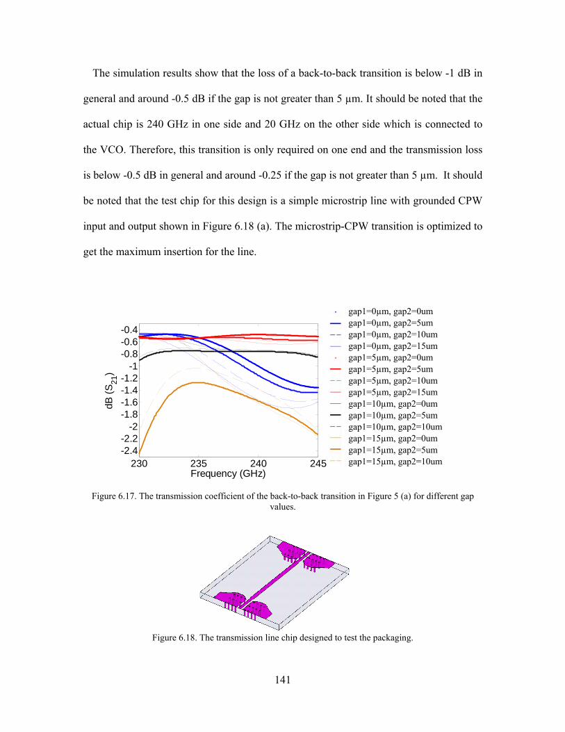
141
The simulation results show that the loss of a back-to-back transition is below -1 dB in
general and around -0.5 dB if the gap is not greater than 5 µm. It should be noted that the
actual chip is 240 GHz in one side and 20 GHz on the other side which is connected to
the VCO. Therefore, this transition is only required on one end and the transmission loss
is below -0.5 dB in general and around -0.25 if the gap is not greater than 5 µm. It should
be noted that the test chip for this design is a simple microstrip line with grounded CPW
input and output shown in Figure 6. 18 (a). The microstrip-CPW transition is optimized to
get the maximum insertion for the line.
230 235 240 245-2.4-2.2
-2-1.8-1.6-1.4-1.2
-1-0.8-0.6-0.4
Frequency (GHz)
dB (
S21
)
Figure 6. 17. The transmission coefficient of the back-to-back transition in Figure 5 (a) for different gap values.
Figure 6. 18. The transmission line chip designed to test the packaging.
gap1=0µm, gap2=0um gap1=0µm, gap2=5um gap1=0µm, gap2=10um gap1=0µm, gap2=15um gap1=5µm, gap2=0um gap1=5µm, gap2=5um gap1=5µm, gap2=10um gap1=5µm, gap2=15um gap1=10µm, gap2=0um gap1=10µm, gap2=5um gap1=10µm, gap2=10um gap1=15µm, gap2=0um gap1=15µm, gap2=5um gap1=15µm, gap2=10um

142
6.3. E-plane Rectangular Waveguide Filter
Waveguide filters, like ordinary filters are designed using reactive elements. These
reactive components are usually realized by inserting discontinuities or obstacles such as
rods or diaphragms along the length of the host waveguide. At microwave and low
MMW frequencies, these filters are fabricated by cutting slits in the cross-section of the
waveguide, inserting the element inside and finally soldering the edges. The structure of
the E-plane rod filter is very much compatible with silicon micromachining. In this
structure, the required susceptance for filter is obtained by metal rods in the E-plane
which extend all the way across the cross section of the waveguide, separated by the
lengths of the waveguide as the impedance transformers as shown in Figure 6. 19 (a).
Depending on the number of poles, it consists of a number of rods serving as inductances
separated by lengths of the waveguide. This structure is simpler than iris, since the inserts
are rod shape and do not deform along the cross-section of waveguide. Therefore, they
can be easily fabricated using single-step etching of silicon. The standard WR-3
waveguide along with rods with h = 432 µm and cross-sections larger than 50 µm × 50
µm – to provide mechanical rigidity - were used to design filters with various passbands.
This filter can be modeled by an equivalent circuit model shown Figure 6. 19 (b). It is
well-known that a rod terminated by the broad wall of a rectangular waveguide acts as an
inductive element whose inductance is inversely proportional to its cross-section size and
the waveguide dimensions. By changing the dimensions of the cross-sections of the rods
the desired inductance values can be designed. The spacing between the rods is an
impedance transformer whose length is a quarter of a guiding wavelength of the
fundamental TE10 mode of the waveguide. Figure 6. 20 (a) shows the response of the full-
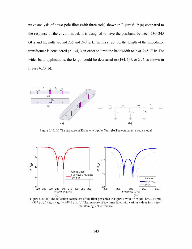
143
wave analysis of a two-pole filter (with three rods) shown in Figure 6. 19 (a) compared to
the response of the circuit model. It is designed to have the passband between 230~245
GHz and the nulls around 235 and 240 GHz. In this structure, the length of the impedance
transformer is considered (2+1/4) λ in order to limit the bandwidth to 230~245 GHz. For
wider band applications, the length could be decreased to (1+1/4) λ or λ /4 as shown in
Figure 6. 20 (b).
(a) (b)
Figure 6. 19. (a) The structure of E-plane two-pole filter. (b) The equivalent circuit model.
220 225 230 235 240 245 250 255 260-80
-60
-40
-20
0
Frequency (GHz)
dB(S
11)
Circuit ModelFull-wave Simulation (HFSS)
220 230 240 250 260
-60
-40
-20
0
Frequency (GHz)
dB(S
11)
l=/4+l=/4+/2l=/4
(a) (b)
Figure 6. 20. (a) The reflection coefficient of the filter presented in Figure 1 with t1=75 µm, l1=2.344 mm, t2=365 µm, l2= l1, t3= t1, l3= 638.6 µm. (b) The response of the same filter with various values for l= l2= l1
maintaining λ /4 difference.

144
220 230 240 250 260
-70
-60
-50
-40
-30
-20
-10
0
Frequency (GHz)
dB
dB(S11
)
dB(S21
)
(a) (b)
Figure 6. 21. (a) The structure of the three-pole filter. (b) The response of the filter for with t1=117 µm, l1= 636 µm, t2=466 µm, l2=1.562 mm, t3= t1, t4= t2, l3= l1, l4= l2
Another filter with three-pole (four rods and three connecting lines) was also designed
for the same frequency band. The total length of this filter is shorter since the spacing is
kept at λ /4 and the roll-off is higher since one more pole is added. The response of the
filter is shown in Figure 6. 21. Higher order filters can also be realized with this method
depending on the application.
6.4. Conclusion
In this chapter, components and techniques required for radar integration were
presented and discussed. These include a transition from CPW to rectangular waveguide,
a transition for embedding external chips and waveguide filters. The components are
designed compatible with micromachining techniques using novel approaches developed
for antenna fabrication.
145
Chapter VII
7. Microfabrication Processes
In this chapter, microfabrication processes for the radar antenna and other components
are presented. As discussed in chapter 4.3, silicon DRIE is a viable approach for
fabrication of high-performance micromachined waveguide structures. In [84] and [85],
both diamond and rectangular waveguide were fabricated by bonding two halves of the
waveguide. A high-precision silicon micromachined waveguide transition with a
capability to integrate filters has been proposed in [86] and shows wideband
characteristics at the same frequency range. However, for higher frequency applications,
these structures show a high degree of fabrication complexity due to error in alignment,
air gaps between conductive parts, poor metal contact, inaccuracy in patterning because
of non-contact lithography, complex assemblies of various parts, and high number of
steps needed for construction which cannot be easily adopted for microfabrication.
Therefore, a novel micromachining process was developed to fabricate the radar
structure.
The proposed structures include the WR-3 waveguide trench and a top cover for lines
and slots for the waveguide slot array antenna and for non-radiating components such as
waveguide transitions and filters. For the final antenna, the patch array which is
suspended on a membrane on top of the waveguide configuration adds one more step to
the fabrication. Therefore, the complete structure is fabricated in three parts as shown in
Figure 7.1; the meander-line waveguide is etched on a wafer, the slots are etched on
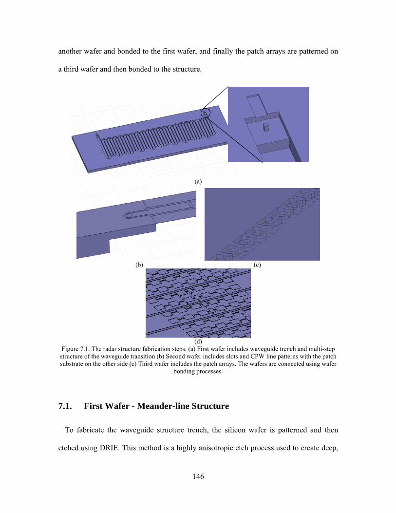
146
another wafer and bonded to the first wafer, and finally the patch arrays are patterned on
a third wafer and then bonded to the structure.
(a)
(b) (c)
(d)
Figure 7.1. The radar structure fabrication steps. (a) First wafer includes waveguide trench and multi-step structure of the waveguide transition (b) Second wafer includes slots and CPW line patterns with the patch substrate on the other side (c) Third wafer includes the patch arrays. The wafers are connected using wafer
bonding processes.
7.1. First Wafer - Meander-line Structure
To fabricate the waveguide structure trench, the silicon wafer is patterned and then
etched using DRIE. This method is a highly anisotropic etch process used to create deep,
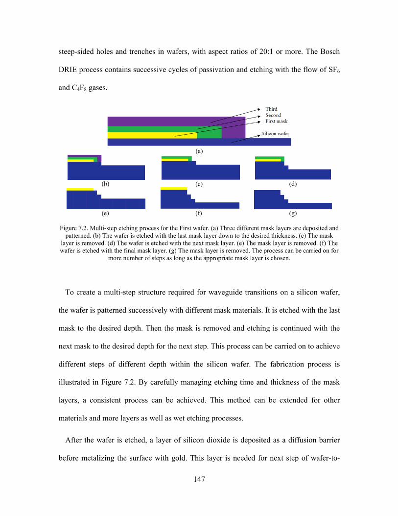
147
steep-sided holes and trenches in wafers, with aspect ratios of 20:1 or more. The Bosch
DRIE process contains successive cycles of passivation and etching with the flow of SF6
and C4F8 gases.
(a)
(b) (c) (d)
(e) (f) (g)
Figure 7.2. Multi-step etching process for the First wafer. (a) Three different mask layers are deposited and
patterned. (b) The wafer is etched with the last mask layer down to the desired thickness. (c) The mask layer is removed. (d) The wafer is etched with the next mask layer. (e) The mask layer is removed. (f) The wafer is etched with the final mask layer. (g) The mask layer is removed. The process can be carried on for
more number of steps as long as the appropriate mask layer is chosen.
To create a multi-step structure required for waveguide transitions on a silicon wafer,
the wafer is patterned successively with different mask materials. It is etched with the last
mask to the desired depth. Then the mask is removed and etching is continued with the
next mask to the desired depth for the next step. This process can be carried on to achieve
different steps of different depth within the silicon wafer. The fabrication process is
illustrated in Figure 7.2. By carefully managing etching time and thickness of the mask
layers, a consistent process can be achieved. This method can be extended for other
materials and more layers as well as wet etching processes.
After the wafer is etched, a layer of silicon dioxide is deposited as a diffusion barrier
before metalizing the surface with gold. This layer is needed for next step of wafer-to-

148
wafer gold bonding to stop diffusion of silicon through the gold layer at high temperature
and pressure and to prevent eutectic bonding. Since our last mask layer is silicon oxide,
we keep it to be used as the diffusion barrier to simplify the process and to avoid adding
one more step. For gold deposition, a sputtering tool with sidewall coverage capability is
used which guarantees coverage of around 50% of the value on the exposed surfaces. In
order to deposit gold, it is necessary to deposit an adhesion layer first. Experiments
showed that a chrome layer alone does not prevent silicon diffusion through gold at high
temperature and pressure. Either titanium or a combination of chrome and titanium with
thicknesses of 300 ~ 500 Ao provides a superior diffusion barrier layer between gold and
silicon. The minimum gold thickness of 1.2 m is needed in order to ensure at least 0.5
m of gold is deposited on the sidewalls.
7.1.1. Requirements for Measurement
7.1.1.a. CPW to CBCPW Transition
The designed low-loss CBCPW line is suspended on a membrane and hence,
measurement probes cannot be placed on it since even a small amount of pressure applied
by the probes might break the membrane. On the other hand, conventional CPW has
substrate and is stiff enough for the probe pressure. Therefore, it is more convenient to
have conventional CPW for measurement purposes so a transition from a conventional
CPW to CBCPW is required to characterize the performance of the transition as shown in
Figure 7.3 (a). For the ease of fabrication and lower loss, a grooved CPW is designed.
The substrate is made of silicon and loss tangent is calculated based on the resistivity of

149
the silicon wafer. It should be noted that the response of the CPW to CBCPW transition
is eventually de-embedded from the final measured results.
There is a difficulty in the fabrication of the grooved CPW and the CBCPW on the
same wafer. The lower wafer on which the cavity of CBCPW and the grooved CPW are
to be fabricated must be metalized, however, the grooves and the backwall of the CPW
cannot be metalized or the CPW will be short-circuited shown in Figure 7.3 (b). In order
to protect these areas from gold deposition, patterning was found to be practically
impossible as was initially envisioned. Spinning photoresist evenly for patterning is not
possible over the grooves. To overcome this problem, we develop a technique based on
the limitation of gold deposition in high aspect ratio features. We have experimentally
shown that when the width of a trench is less than 5 m and the aspect ratio is higher than
10, gold is not deposited on the bottom and lower portion of the side walls of the trench.
Figure 7.3 (c) shows the desired short segment of grooved CPW, which is fabricated with
the so called “shadow walls” as shown in Figure 7.3 (d). In this structure the thin
protecting walls shadow gold deposition because of the high aspect ratio of the channels.
After gold deposition, since the bottom the sides of the shadow walls are not covered
with gold, they can be removed using isotropic silicon etchants like xenon difluoride
(XeF2) or sulfur hexafluoride (SF6). The etch time depends on the gap width between the
walls and is longer for thinner and deeper gaps as it is hard for the gas to penetrate inside
these areas. However, in order to reduce damage to other areas, the wafer is exposed to
the etchant over a relatively short period of time to make the walls frail. Ultrasonic
vibration is then used to remove the fragile walls completely. Figure 7.4 (a) and (b) show
the structure before and after etching the shadow walls. The walls are completely
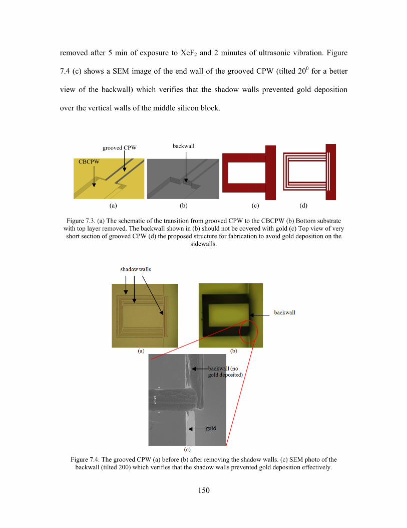
150
removed after 5 min of exposure to XeF2 and 2 minutes of ultrasonic vibration. Figure
7.4 (c) shows a SEM image of the end wall of the grooved CPW (tilted 200 for a better
view of the backwall) which verifies that the shadow walls prevented gold deposition
over the vertical walls of the middle silicon block.
(a) (b) (c) (d)
Figure 7.3. (a) The schematic of the transition from grooved CPW to the CBCPW (b) Bottom substrate with top layer removed. The backwall shown in (b) should not be covered with gold (c) Top view of very short section of grooved CPW (d) the proposed structure for fabrication to avoid gold deposition on the
sidewalls.
Figure 7.4. The grooved CPW (a) before (b) after removing the shadow walls. (c) SEM photo of the
backwall (tilted 200) which verifies that the shadow walls prevented gold deposition effectively.
grooved CPW CBCPW
backwall
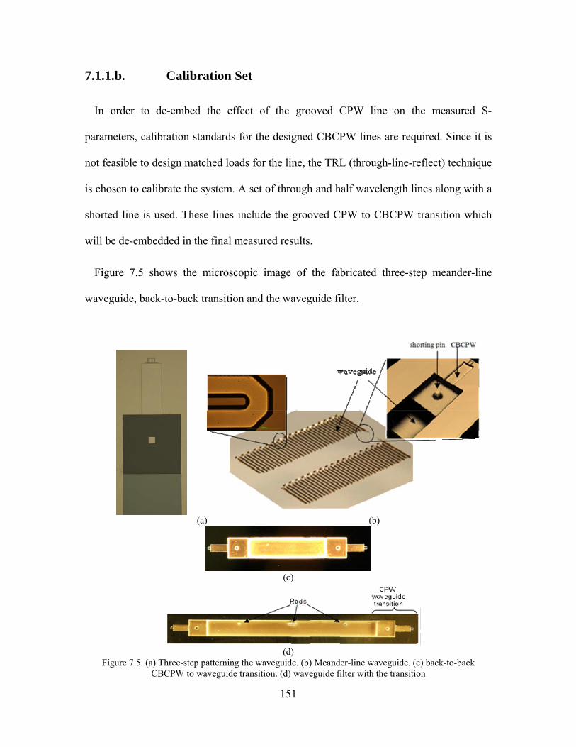
151
7.1.1.b. Calibration Set
In order to de-embed the effect of the grooved CPW line on the measured S-
parameters, calibration standards for the designed CBCPW lines are required. Since it is
not feasible to design matched loads for the line, the TRL (through-line-reflect) technique
is chosen to calibrate the system. A set of through and half wavelength lines along with a
shorted line is used. These lines include the grooved CPW to CBCPW transition which
will be de-embedded in the final measured results.
Figure 7.5 shows the microscopic image of the fabricated three-step meander-line
waveguide, back-to-back transition and the waveguide filter.
(a) (b)
(c)
(d)
Figure 7.5. (a) Three-step patterning the waveguide. (b) Meander-line waveguide. (c) back-to-back CBCPW to waveguide transition. (d) waveguide filter with the transition

152
7.2. Second Wafer –Slots / Patch Array Substrate
A second wafer is used to cover the top part of the meander-line structure, which
includes the CPW lines and slots. This wafer also serves as the substrate of the patch
arrays. Two variations of the structure were fabricated at this stage. A simpler process
was developed to fabricate the transition, filters and slot-waveguide antenna. A second
process is proposed to fabricate the hybrid-coupled patch array which needs a third wafer.
Since the CBCPWs are suspended on a thin membrane layer, a stacked layer of
LPCVD SiO2/Si3N4/SiO2 (ONO) is first deposited on top of the second wafer. This layer
provides a small amount of tensile stress so that the membrane does not buckle after the
wafer release. The wafer is then gold-coated with an adhesion layer, and then patterned
and etched to form the CPW lines as well as the slots. Then it is flipped over and the
backside is etched to form openings on top of the CBCPW and the slots. The structure is
suspended on a membrane around the open areas of the wafer and should be carefully
handled. Figure 7.6 illustrates the fabrication process of this wafer and Figure 7.7 shows
the fabricated CPW lines and slots on the gold side of the wafer.
At this stage, the first and second wafers should be bonded. Since the wafers are gold
covered, we have to perform gold-to-gold thermocompression bonding. This bonding
technique provides a hermetic of the surfaces and guarantees the continuity of the current
flow. One concern however, is diffusion of silicon through gold, introducing impurities
and failure in bonding. To overcome this problem, as mentioned before, a SiO2 diffusion
barrier layer before gold deposition is necessary [87]. The stacked membrane layer
already serves as the diffusion barrier on the second wafer
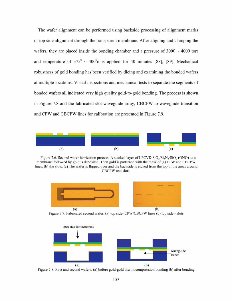
153
The wafer alignment can be performed using backside processing of alignment marks
or top side alignment through the transparent membrane. After aligning and clamping the
wafers, they are placed inside the bonding chamber and a pressure of 3000 ~ 4000 torr
and temperature of 3750 ~ 4000c is applied for 40 minutes [88], [89]. Mechanical
robustness of gold bonding has been verified by dicing and examining the bonded wafers
at multiple locations. Visual inspections and mechanical tests to separate the segments of
bonded wafers all indicated very high quality gold-to-gold bonding. The process is shown
in Figure 7.8 and the fabricated slot-waveguide array, CBCPW to waveguide transition
and CPW and CBCPW lines for calibration are presented in Figure 7.9.
(a) (b) (c)
Figure 7.6. Second wafer fabrication process. A stacked layer of LPCVD SiO2/Si3N4/SiO2 (ONO) as a membrane followed by gold is deposited. Then gold is patterned with the mask of (a) CPW and CBCPW
lines. (b) the slots. (c) The wafer is flipped over and the backside is etched from the top of the areas around CBCPW and slots.
(a) (b)
Figure 7.7. Fabricated second wafer. (a) top side- CPW/CBCPW lines (b) top side - slots
(a) (b) Figure 7.8. First and second wafers. (a) before gold-gold thermocompression bonding (b) after bonding
waveguide trench

154
(a) (b) (c)
(d) (e)
(f)
Figure 7.9. (a) First wafer before bonding. (b) the meander-line slot antenna after bonding, (c) the low-loss design (d) the CBCPW/waveguide transition, (e) the CPW/CBCPW transition, (f) calibration standards,
from left to right: thru, line, open, short, offset short.
To fabricate the patch array version of the antenna structure, after CPW/slot patterning
on the second wafer, the backside is etched with a different pattern. While silicon is still
completely removed from the areas around the CBCPW membrane, the pattern of the
patch substrate is etched around the slots with the pattern shown in Figure 7.10 (a). We
perform a multi-step etching for the substrate with a similar process mentioned for the
first wafer with the membrane as the etch stop of the process. Then the substrate is gold-

155
coated as shown in Figure 7.10 (b). Due to the RIE lag effect, the etch depth is dependent
on the etched area, i. e., it is deeper for larger areas. Figure 7.10 (c) shows a more
realistic figure of what is realized after etching. This issue is addressed by simulating
such a structure. The results show a similar performance for etches deeper than 60%
which indicates the steps do not cause a noteworthy change in the antenna pattern and the
reflection loss.
The wafer is then bonded to the first wafer as shown in Figure 7.11 with the same gold-
gold bonding process. Figure 7.12 shows the fabricated patch array substrate.
(a) (b)
(c)
Figure 7.10. (a) multi-step etching for the patch array substrate. Thin shadow walls are also formed to protect the sidewalls of the silicon block from gold-deposition. (b) gold-coating the substrate. (c) the
realistic version of the structure.
(a) (b)
Figure 7.11. First and second wafers. (a) before gold-gold thermocompression bonding (b) after bonding
deeper shallower

156
Figure 7.12. Fabricated patch array substrate
7.3. Third Wafer –Patch Array
The patch array structure consists of 36 × 2 = 72 (two in each turn) seven-element
patch sub-arrays (total of 504 patches). The array has to be suspended over a membrane
on top of the air substrate. Initially, stacked layers of ONO, SU-8 and PDMS (a
polymeric organosilicon compound) were tested to serve as membranes. In these
processes, the membrane layer is first deposited on a silicon wafer. Then gold is
deposited and etched to form patch arrays. This wafer had to be bonded to the bonded
pair of first and second wafer. After bonding, the silicon of the third wafer should be
removed to have the patches suspended on the membrane. For this purpose, both wafer
release and wafer etching techniques can be used. For the wafer release, a release layer
such as photoresist should be used before the membrane layer. However, releasing a
wafer involves a wet etching process after bonding which cannot be used due to
penetration of the solvent to the bottom layers. Dry etching of the whole wafer did not
work either since etching is not uniform. It attacks the edges and areas around the
circumference of the wafer strongly. The only other way is removing the top wafer
locally only around patch areas using DRIE.

157
The choice of bonding method is flexible since here no high quality adhesion is needed.
If the membrane is ONO, diffusion or anodic bonding can be used. However, the main
issue with the ONO layer is that it cannot be suspended over a large area. SU-8 cracks at
temperatures above 1500C, so a low temperature bonding method should be used. One
way is to use a photo-patternable glue applied on the wafers. Unfortunately, such a
material was not available. Photoresist is the only known choice but it outgases and
losses its adhesive properties when it is placed inside the DRIE chamber. Crystalbond LT
which is used for temporarily mounting in microfabrication was another option. The
material can be diluted with acetone and spun, but cannot be not patterned, it has to be
applied manually and therefore the thickness cannot be controlled which causes gap
between patches and substrate. However, since the adhesive properties are very good, it
was used to test the SU-8 membrane. Nevertheless, during the wafer removal process, the
membrane collapses around the edges, while silicon is still left around the center. SU-8
layer can be more efficient if the wafer removal process is improved.
Using polymer bonding techniques with a polymer membrane is another option. In
order to avoid all the above problems a membrane transfer technique with Parylene [90]
was used. The fabrication process is illustrated in Figure 7.13. First, to make a membrane
layer with a low adhesion with the wafer, a layer of a photoresist (as a release layer) is
spun on the unpolished side of a silicon wafer and baked. Using the unpolished side of
the wafer helps decrease the adhesion of the Parylene layer to silicon after removing the
release layer. Then, a layer of Parylene with 5 ~ 15 um thickness and then gold is
deposited and patterned to form the patch arrays. At the last step, we make some cuts on
the Parylene around the circumference of the wafer to provide access to the bottom

158
photoresist layer. The wafer is soaked in acetone and then IPA (isopropyl alcohol)
solutions for several days to dissolve the photoresist completely as shown in Figure 7.13
(b). The fabricated third wafer is shown in Figure 7.14.
Since Parylene, like other polymers, very efficiently bonds to itself, the gold-bonded
pair should also be covered with Parylene first as shown in Figure 7.15 (a). This layer
could be very thin (< 5 µm) in order not to affect the patch array loss. Parylene bonding is
performed under vacuum in order to avoid Parylene interaction with oxygen and nitrogen
at 150+ 0C and 800 N force over a 4 inch wafer for 30~40 minutes. For this very
structure, bonding pressure should be much higher (5000 ~ 7000 N) than usual since the
gold-bonded pair is bowed by a small amount and we have to compensate for it to make
sure the Parylene layers are in contact everywhere on the wafer.
The patch array membrane is transferred after bonding. A razor blade can used to cut
the Parylene from the circumference of the third wafer so that the wafer is debonded and
released as shown in Figure 7.15 (d). Since the Parylene from the patch wafer is
connected to the bottom Parylene wafer, this method is called the Parylene transfer
method [90]. Figure 7.14 shows the fabricated Parylene membrane.
(a) (b)
Figure 7.13. Third wafer fabrication process. (a) photoresist, Parylene and patterned gold are deposited on a silicon wafer. (b) photoresist is dissolved by soaking the wafer in acetone and IPA.

159
Figure 7.14. Fabricated third wafer after dissolving the photoresist release layer.
(a) (b)
(c) (d)
Figure 7.15. Last step of the fabrication process. (a) The gold-bonded pair is Parylene-coated. (b) The wafers are aligned and (c) bonded. (d) The third wafer is de-bonded with a razor blade through the edges.
cuts for dissolving photoresist
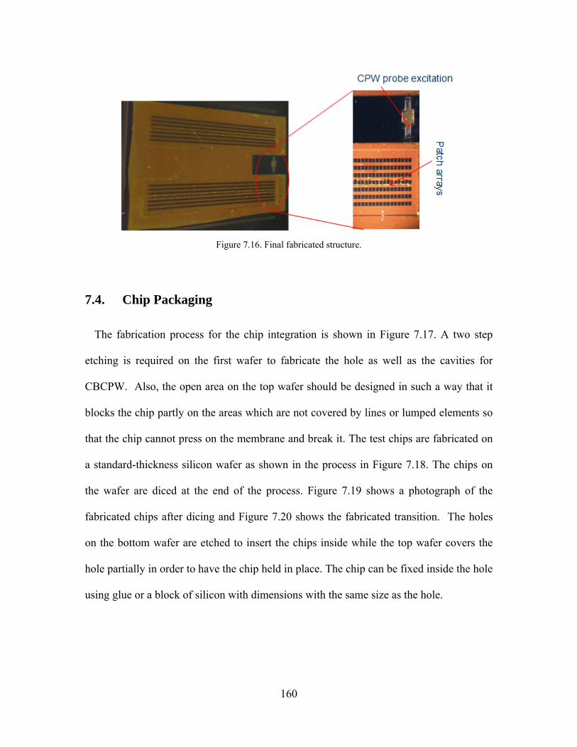
160
Figure 7.16. Final fabricated structure.
7.4. Chip Packaging
The fabrication process for the chip integration is shown in Figure 7.17. A two step
etching is required on the first wafer to fabricate the hole as well as the cavities for
CBCPW. Also, the open area on the top wafer should be designed in such a way that it
blocks the chip partly on the areas which are not covered by lines or lumped elements so
that the chip cannot press on the membrane and break it. The test chips are fabricated on
a standard-thickness silicon wafer as shown in the process in Figure 7.18. The chips on
the wafer are diced at the end of the process. Figure 7.19 shows a photograph of the
fabricated chips after dicing and Figure 7.20 shows the fabricated transition. The holes
on the bottom wafer are etched to insert the chips inside while the top wafer covers the
hole partially in order to have the chip held in place. The chip can be fixed inside the hole
using glue or a block of silicon with dimensions with the same size as the hole.

161
(a) (b) (c)
(d) (e) (f)
Figure 7.17 Fabrication process of the transition between the chip and the CBCPW. (a) two-step pattering
(b) two step etching (c) gold sputtering for the first wafer. (d) top wafer (membrane, line patterns and etching the open areas). (e) top-bottom wafers gold bonding. (f) inserting the chip inside.
(a) (b)
Figure 7.18. Fabrication process of a test chip (a) pattering gold on a silicon wafer (b) etching the backside of the wafer to thin down to the desired chip thickness.
(a)
Figure 7.19. (a) the chip is fabricated on a silicon wafer with a simple CPW to microstrip transtion optimized for maximum insertion.

162
(b)
Figure 7.20. The bottom and the top wafer of the fabricated transition. It is observed that the holes on the bottom wafers are partially covered by the top wafer.
7.5. Estimation of the Cost
Microfabrication is low-cost because many of the processes can be performed in
parallel with multiple components on a single wafer. This includes most of the
depositions and wet etchings. In addition, the cost of fabrication on a 6 inch or larger
wafers is commonly equal to that on a 4 inch wafer, but since the yield is higher with
larger wafers, cost can be considerably decreased. Figure 7.21 shows the yield of the
radar structure with 4 inch and 6 inch wafers. The cost of process remains the same, yet
the yield with 6 inch wafers is 4 times higher. Table X lists the estimated cost and time of
microfabrication for different processes on a 6 inch wafer. Processes such as PVD and
LPCVD depositions, although long and costly, have the same wafer process cost and time
so the components cost much lower due to wafer parallel processing.
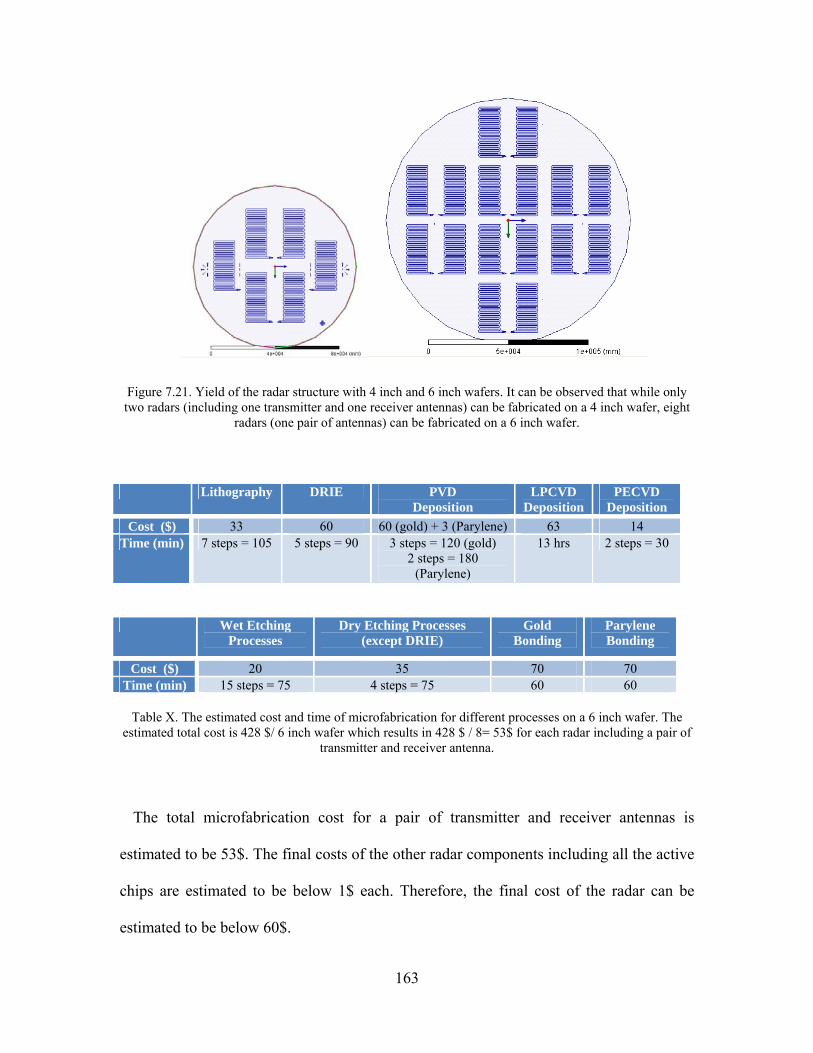
163
Figure 7.21. Yield of the radar structure with 4 inch and 6 inch wafers. It can be observed that while only two radars (including one transmitter and one receiver antennas) can be fabricated on a 4 inch wafer, eight
radars (one pair of antennas) can be fabricated on a 6 inch wafer.
Lithography DRIE PVD Deposition
LPCVD Deposition
PECVD Deposition
Cost ($) 33 60 60 (gold) + 3 (Parylene) 63 14 Time (min) 7 steps = 105 5 steps = 90 3 steps = 120 (gold)
2 steps = 180 (Parylene)
13 hrs 2 steps = 30
Wet Etching Processes
Dry Etching Processes (except DRIE)
Gold Bonding
Parylene Bonding
Cost ($) 20 35 70 70 Time (min) 15 steps = 75 4 steps = 75 60 60
Table X. The estimated cost and time of microfabrication for different processes on a 6 inch wafer. The
estimated total cost is 428 $/ 6 inch wafer which results in 428 $ / 8= 53$ for each radar including a pair of transmitter and receiver antenna.
The total microfabrication cost for a pair of transmitter and receiver antennas is
estimated to be 53$. The final costs of the other radar components including all the active
chips are estimated to be below 1$ each. Therefore, the final cost of the radar can be
estimated to be below 60$.

164
7.6. Conclusion
In this chapter, the details of microfabrication processes of the proposed structures
were discussed. The process is performed on three separate silicon wafers each of which
include a part of the antenna and other passive devices which are bonded together at the
final step. Various microfabrication procedures such as silicon DRIE, gold deposition,
multi-step mask deposition, silicon-dioxide deposition, low-stress silicon-dioxide/silicon
nitride deposition, XeF2 silicon etching, gold-gold thermocompression bonding, topside
and backside wafer alignment, polymer deposition, polymer bonding, etc. are employed
and optimized for the fabrication of the radar components.

165
Chapter VIII
8. On-Wafer Y-band Measurements
Making accurate and reliable measurements at high MMW frequencies is a challenging
task and demands high quality instrumentation. MMW frequency extenders are used
along with vector network analyzers to provide the signal at the desired frequency band.
The measurement at the high MMW frequencies especially Y-band have been more
focused on WR-3 rectangular waveguide devices [91] - [94]. Although there are some
difficulties associated with waveguide measurement such as poor interconnectability
between the DUT and the waveguide flange at the test port, it has been shown to be more
convenient and reliable than on-wafer measurements. The first full two-port on-wafer
measurement capability up to 220 GHz was reported in 1999 [95]. Since then further
developments have enabled full two-port on-wafer VNA measurements up to higher
frequencies [96]. The Y-band measurements have been recently facilitated using OML
[97] and VDI [98] frequency extenders connected to the PNA-X. The on-wafer
measurements are conducted using ground-signal-ground (GSG) picoprobes used to
excite the CPW lines on the DUT.
In this chapter, the measurement setup for full two-port S-parameter measurements of
waveguide transitions and filters is first introduced and the results of the measurement are
presented. The antenna radiation pattern measurement setup is then described and the
radiation pattern of a standard E-plane horn antenna and the waveguide slot array are
measured with this system and discussed.

166
8.1. S-parameter Measurement
On-wafer S-parameter measurements of the fabricated waveguide transitions and filters
are performed using the dual source PNA-X with OML frequency extenders shown in
Figure 8.1. The setup includes:
1. Agilent PNA-X N5245A
2. OML frequency extending modules
3. GGB 220-325 GHz GSG probes with 80 µm pitch size
4. WR-3 bent waveguides
5. Cascade MMW probe station and micropositioners
6. Leica S8APO stereomicroscope
The configuration is assembled in such a way as to provide a system with high
reliability and capability to easily move and control the GSG probe location. The devices
under test are fed through the probes connected to the frequency extending modules using
WR-3 bent waveguides controlled by Cascade Microtech MMW micropositioners. The
On-substrate TRL calibration set as shown in Figure 8.2 is measured first to de-embed
the effect of the CPW line. In addition, the response of a back-to-back transition is also
de-embedded from the final response of the structures by measuring the fabricated
calibration lines shown in Figure 7.9. (e). After calibration, the S-parameters of the
devices were measured and are presented in Figure 8.3 and Figure 8.4 for the CBCPW to
waveguide transition and waveguide filters. The measurement results show good
agreements with the simulation. The deviation can be mainly attributed to the error in the
probe placement and establishing good contacts on the pads. In addition, the quality of
gold bonding and high quality ohmic contact as well as the deviation of the dimensions

167
(especially depth) of the fabricated structures from the designed ones cause differences
between the measured and simulated results.
Figure 8.1. WR-3 (220-325 GHz) measurement setup.

168
Figure 8.2. GGB CS-15 calibration substrate with line, thru, matched load, short and open.
220 225 230 235 240 245 250 255 260 265-5.5
-5
-4.5
-4
-3.5
-3
-2.5
-2
-1.5
-1
-0.5
0
Frequency (GHz)
S2
1(d
B)
SimulationMeasurement
220 225 230 235 240 245 250 255 260 265-60
-50
-40
-30
-20
-10
0
Frequency (GHz)
S1
1(d
B)
SimulationMeasurement
(a) (b)
Figure 8.3. The measured transmission and reflection coefficients of the back-to-back transition structure of Figure 6.4. The results are in good agreement with the simulation. The transmission coefficient is below -
1.5 dB for the two series transitions and the waveguide section in between.
220 230 240 250 260-45
-35
-25
-15
-5
0
Frequency (GHz)
dB(S
11)
MeasurementSimulation
220 230 240 250 260-20
-15
-10
-5
0
Frequency (GHz)
dB(S
21)
MeasurementSimulation
(a) (b)
Figure 8.4. The measured (a) reflection and (b) transmission coefficient of the filter shown in Figure 6. 19 compared to the full-wave simulation. The nulls of the filter are precisely detected and the results are in
good agreement with the simulation.

169
8.2. Antenna Radiation Pattern Measurement
At Y-band frequencies - due to the large free space path loss (80 dB + 20 log(d)) – the
received far-field signals commonly fall below the dynamic range of the measurement
system. In particular, this is the case when the apertures of the antennas are large
compared to the wavelength so that their far-field distance is more than a meter away. For
this antenna with 4.5 cm aperture length, 2D2/ > 3 m. Since the dynamic range of the
system is around 75 dB, measuring the far field of the antenna is not practical.
In the recent years, the near-field antenna pattern measurement technique has become a
popular alternative to the standard far-field measurement method. Characterization of
radiation properties of antennas using a near-field technique is based on the measurement
of both magnitude and phase of the electric field in the vicinity of the antenna. Based on
the uniqueness theorem, using the tangential electric field over a closed surface, the field
everywhere outside the source region can be uniquely evaluated. Therefore, first the near-
field of the antenna should be measured over an area. A probe is moved on a near-field
rectangular area above the antenna and by scanning the field at each point generates a
grid. Spatial resolution and the extent of the scanned area, the probe distance from the
antenna and the precision in positioning the probe are critical parameters for accurate
measurement. The extent of the scanned area is determined by the truncation spatial
frequency fx = 1
2 x, where 0 / 2( 1)x is the spatial resolution. The attenuation
of the non-propagating wave can be obtained from: 2
2 20 0
11z xk k k
,
therefore the loss factor is calculated as ( )zdL dB e , where d = 0 is the distance from
170
the antenna to the probe. Upon substituting d and z ,2
154.58 1L dB
which
establishes a relationship between spatial resolution and the probe distance to the antenna
for a chosen loss factor.
The setup shown in Figure 8.5 was used to measure the antenna near-field. The antenna
is fed through the CPW to waveguide transition using GSG probes connected to a
frequency extender. To measure both x- and y-directed radiated electric fields, two WR3
open-ended waveguides with thinned walls to minimize reflection from the waveguide
probe, one straight and one twisted, for both Ex and Ey measurements as shown in Figure
8.6 are used. They are placed at the near-field region on top of the antenna while their
other end is connected to the other frequency multiplier which is mounted on top of an
XY stage as shown in Figure 8.7. The high-resolution XY linear stage is utilized to move
the waveguide probe in a grid and collect the data. The stage consists of two orthogonal
ballscrew linear stages with brushless servomotor and line encoders mounted atop of each
other and are separately controlled by two PWM digital controllers. A Matlab code was
developed to simultaneously control the stage and collect S21 data from the PNA-X. In
order to have maximum dynamic range and stable measured data, the PNA-X is set to
have 300 Hz IF bandwidth and averaging factor of 8.

171
Figure 8.5. The proposed setup to measure the antenna near-field.
(a)
(b)
Figure 8.6. (a) Straight and (b) twisted waveguide probes to measure co- and cross-polarized field components.
Figure 8.7. The XY stage used to move the near-field waveguide probe.
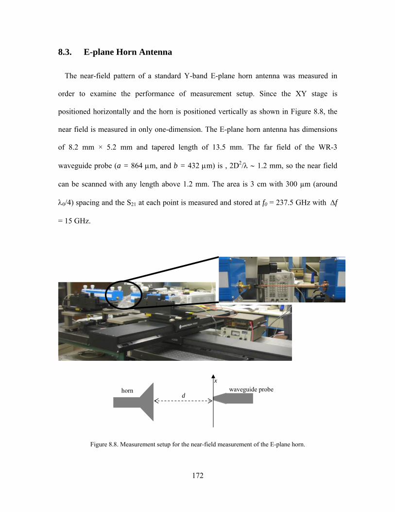
172
8.3. E-plane Horn Antenna
The near-field pattern of a standard Y-band E-plane horn antenna was measured in
order to examine the performance of measurement setup. Since the XY stage is
positioned horizontally and the horn is positioned vertically as shown in Figure 8.8, the
near field is measured in only one-dimension. The E-plane horn antenna has dimensions
of 8.2 mm × 5.2 mm and tapered length of 13.5 mm. The far field of the WR-3
waveguide probe (a = 864 m, and b = 432 m) is , 2D2/ 1.2 mm, so the near field
can be scanned with any length above 1.2 mm. The area is 3 cm with 300 µm (around
0/4) spacing and the S21 at each point is measured and stored at f0 = 237.5 GHz with f
= 15 GHz.
Figure 8.8. Measurement setup for the near-field measurement of the E-plane horn.
x d
horn waveguide probe
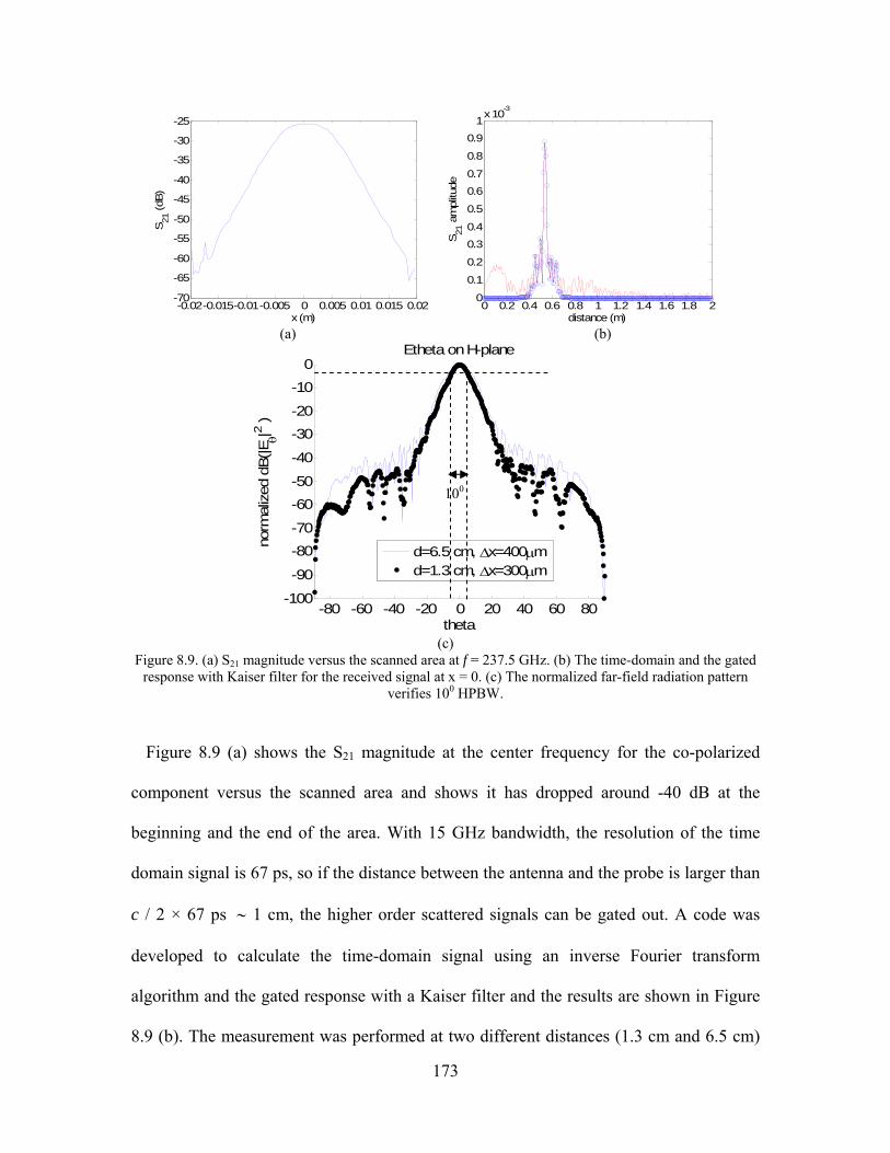
173
-0.02-0.015-0.01-0.005 0 0.005 0.01 0.015 0.02-70
-65
-60
-55
-50
-45
-40
-35
-30
-25
x (m)
S21 (
dB)
0 0.2 0.4 0.6 0.8 1 1.2 1.4 1.6 1.8 20
0.1
0.2
0.3
0.4
0.5
0.6
0.7
0.8
0.9
1x 10
-3
distance (m)
S21 a
mpl
itude
(a) (b)
(c)
Figure 8.9. (a) S21 magnitude versus the scanned area at f = 237.5 GHz. (b) The time-domain and the gated response with Kaiser filter for the received signal at x = 0. (c) The normalized far-field radiation pattern
verifies 100 HPBW.
Figure 8.9 (a) shows the S21 magnitude at the center frequency for the co-polarized
component versus the scanned area and shows it has dropped around -40 dB at the
beginning and the end of the area. With 15 GHz bandwidth, the resolution of the time
domain signal is 67 ps, so if the distance between the antenna and the probe is larger than
c / 2 × 67 ps 1 cm, the higher order scattered signals can be gated out. A code was
developed to calculate the time-domain signal using an inverse Fourier transform
algorithm and the gated response with a Kaiser filter and the results are shown in Figure
8.9 (b). The measurement was performed at two different distances (1.3 cm and 6.5 cm)
-80 -60 -40 -20 0 20 40 60 80-100
-90
-80
-70
-60
-50
-40
-30
-20
-10
0Etheta on H-plane
theta
norm
aliz
ed d
B(|E
|2 )
d=6.5 cm, x=400m d=1.3 cm, x=300m
100
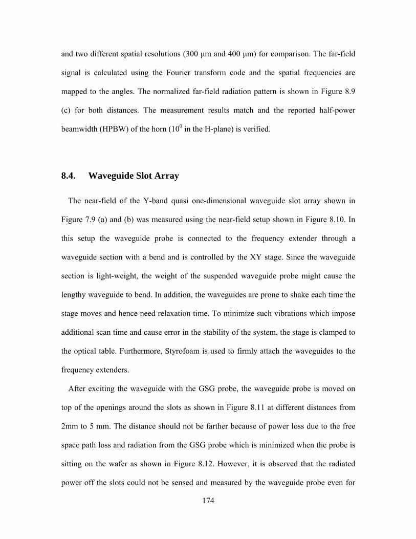
174
and two different spatial resolutions (300 μm and 400 μm) for comparison. The far-field
signal is calculated using the Fourier transform code and the spatial frequencies are
mapped to the angles. The normalized far-field radiation pattern is shown in Figure 8.9
(c) for both distances. The measurement results match and the reported half-power
beamwidth (HPBW) of the horn (100 in the H-plane) is verified.
8.4. Waveguide Slot Array
The near-field of the Y-band quasi one-dimensional waveguide slot array shown in
Figure 7.9 (a) and (b) was measured using the near-field setup shown in Figure 8.10. In
this setup the waveguide probe is connected to the frequency extender through a
waveguide section with a bend and is controlled by the XY stage. Since the waveguide
section is light-weight, the weight of the suspended waveguide probe might cause the
lengthy waveguide to bend. In addition, the waveguides are prone to shake each time the
stage moves and hence need relaxation time. To minimize such vibrations which impose
additional scan time and cause error in the stability of the system, the stage is clamped to
the optical table. Furthermore, Styrofoam is used to firmly attach the waveguides to the
frequency extenders.
After exciting the waveguide with the GSG probe, the waveguide probe is moved on
top of the openings around the slots as shown in Figure 8.11 at different distances from
2mm to 5 mm. The distance should not be farther because of power loss due to the free
space path loss and radiation from the GSG probe which is minimized when the probe is
sitting on the wafer as shown in Figure 8.12. However, it is observed that the radiated
power off the slots could not be sensed and measured by the waveguide probe even for

175
the co-polarized field element. This can be attributed to the very narrow initial slots (5
µm as represented in the inset) and low dynamic range and high loss in the system
imposed by long waveguide sections and GSG probes.
Figure 8.10. The setup proposed for the antenna measurement. The antenna is excited through the GSG probes and the radiated power is measured with a waveguide probe. The waveguide probe is connected to
the frequency extender through a waveguide bend and its position is controlled by the XY stage.
Figure 8.11. The waveguide probe moving on top of the slot openings.
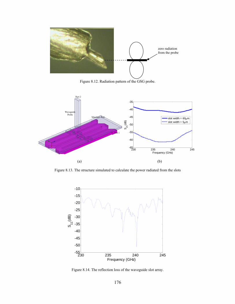
176
Figure 8.12. Radiation pattern of the GSG probe.
230 235 240 245-65
-60
-55
-50
-45
-40
-35
Frequency (GHz)
S2
1(d
B)
slot width = 60mslot width = 5m
(a) (b)
Figure 8.13. The structure simulated to calculate the power radiated from the slots
230 235 240 245-55
-50
-45
-40
-35
-30
-25
-20
-15
-10
Frequency (GHz)
S11
(dB
)
Figure 8.14. The reflection loss of the waveguide slot array.
Port 1
Port 2
Matched Port
Waveguide Probe
zero radiation from the probe
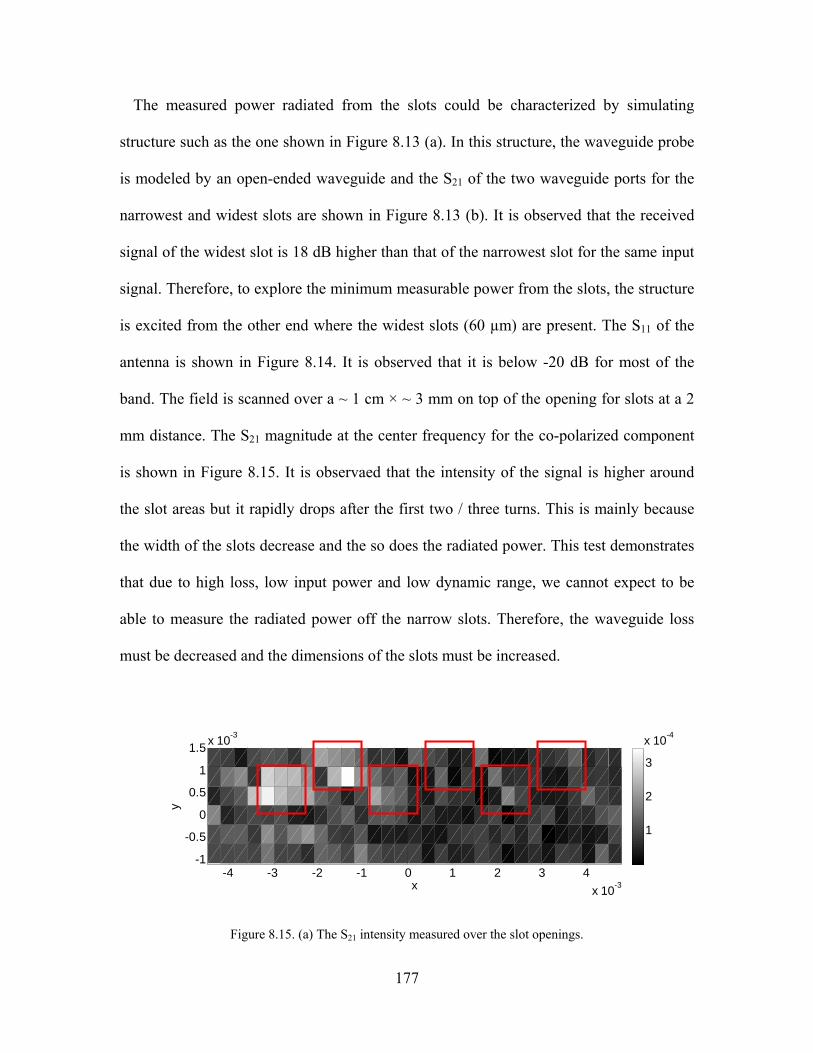
177
The measured power radiated from the slots could be characterized by simulating
structure such as the one shown in Figure 8.13 (a). In this structure, the waveguide probe
is modeled by an open-ended waveguide and the S21 of the two waveguide ports for the
narrowest and widest slots are shown in Figure 8.13 (b). It is observed that the received
signal of the widest slot is 18 dB higher than that of the narrowest slot for the same input
signal. Therefore, to explore the minimum measurable power from the slots, the structure
is excited from the other end where the widest slots (60 µm) are present. The S11 of the
antenna is shown in Figure 8.14. It is observed that it is below -20 dB for most of the
band. The field is scanned over a ~ 1 cm × ~ 3 mm on top of the opening for slots at a 2
mm distance. The S21 magnitude at the center frequency for the co-polarized component
is shown in Figure 8.15. It is observaed that the intensity of the signal is higher around
the slot areas but it rapidly drops after the first two / three turns. This is mainly because
the width of the slots decrease and the so does the radiated power. This test demonstrates
that due to high loss, low input power and low dynamic range, we cannot expect to be
able to measure the radiated power off the narrow slots. Therefore, the waveguide loss
must be decreased and the dimensions of the slots must be increased.
Figure 8.15. (a) The S21 intensity measured over the slot openings.
-4 -3 -2 -1 0 1 2 3 4
x 10-3
-1
-0.5
0
0.5
1
1.5x 10
-3
x
y
1
2
3
x 10-4

178
The reduced-loss waveguide with larger slots proposed in section 5.7 (Figure 7.9) was
then measured with the same setup. The field is scanned over ~ 1.2 cm × ~ 3 mm on top
of the opening for slots at 1.5 mm distance. The S21 magnitude at the center frequency for
the co-polarized component is shown in Figure 8.16 (a). It is observed that the intensity
of the radiated signal is decayed along the length of the antenna. Figure 8.16 (b) plots the
intensity on top of the first 10 slots area along the line shown in Figure 8.16 (a) and
shows around a 20 dB loss which is much higher than expected. The time-domain signal
using inverse Fourier Transform algorithm at two different spots is shown in Figure 8.17.
Since the amplitude of the main signal is higher than any other interference, we do not
use time gating to evaluate the far-field. An advantage of not using time-gating is the
ability to keep the information from the whole band and verify the frequency scanning
behavior of the antenna.
(a)
-6 -4 -2 0 2 4 6
x 10-3
-100
-95
-90
-85
-80
-75
-70
-65
-60
-55
x
S21 (dB
)
(b)
Figure 8.16. (a) S21 intensity measured over the slot openings of the reduced-loss design. (b) S21 intensity over the cells shown in part (a).
-5 -4 -3 -2 -1 0 1 2 3 4 5 6
x 10-3
-5
0
5
10
x 10-4
x
y
24681012
x 10-4
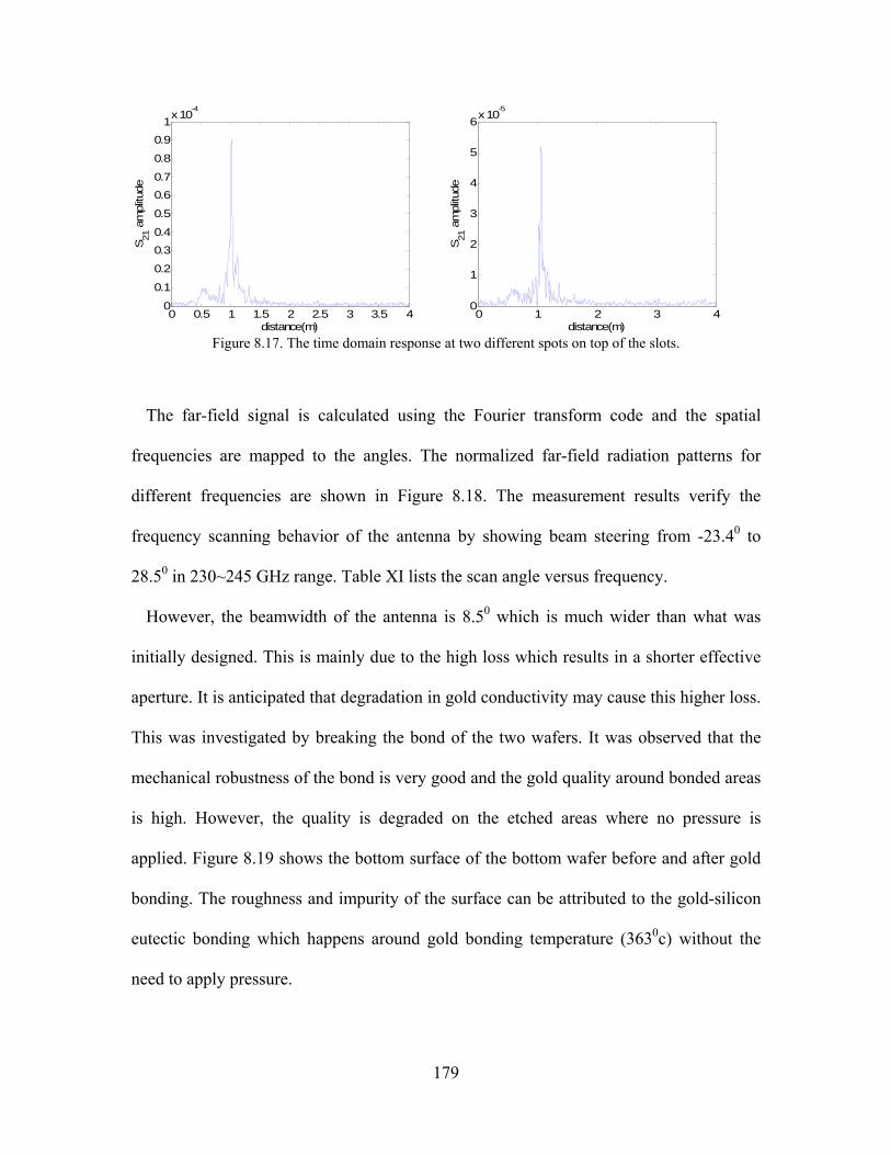
179
0 0.5 1 1.5 2 2.5 3 3.5 40
0.1
0.2
0.3
0.4
0.5
0.6
0.7
0.8
0.9
1x 10
-4
distance(m)
S21 a
mpl
itude
0 1 2 3 40
1
2
3
4
5
6x 10
-5
distance(m)
S21 a
mpl
itude
Figure 8.17. The time domain response at two different spots on top of the slots.
The far-field signal is calculated using the Fourier transform code and the spatial
frequencies are mapped to the angles. The normalized far-field radiation patterns for
different frequencies are shown in Figure 8.18. The measurement results verify the
frequency scanning behavior of the antenna by showing beam steering from -23.40 to
28.50 in 230~245 GHz range. Table XI lists the scan angle versus frequency.
However, the beamwidth of the antenna is 8.50 which is much wider than what was
initially designed. This is mainly due to the high loss which results in a shorter effective
aperture. It is anticipated that degradation in gold conductivity may cause this higher loss.
This was investigated by breaking the bond of the two wafers. It was observed that the
mechanical robustness of the bond is very good and the gold quality around bonded areas
is high. However, the quality is degraded on the etched areas where no pressure is
applied. Figure 8.19 shows the bottom surface of the bottom wafer before and after gold
bonding. The roughness and impurity of the surface can be attributed to the gold-silicon
eutectic bonding which happens around gold bonding temperature (3630c) without the
need to apply pressure.

180
(a) (b) (c) (d) (e)
Figure 8.18. (a) Far-field radiation pattern at different frequencies, beamwidth = 8.50.
Frequency (GHz) Scan Angle (deg) 230 -23.4053
231.5 -17.5268 233 -11.6482
234.5 -5.7124 236 -1.1459
237.5 2.8762 239 8.7032
240.5 14.7422 242 19.3431 245. 28.5448
Table XI. The scan angle versus frequency for the waveguide slot array.
(a) (b) Figure 8.19. Etched area of the bottom wafer (a) before and (b) after bonding. The SEM photo in the inset
shows around 5~10 µm roughness.

181
In order to resolve this issue, an extra layer of a diffusion barrier material (SiO2) is
deposited on the bottom wafer right before gold deposition. Figure 8.20 shows the
transition area after the bonding for both cases. The microscope is focused on the bottom
wafer through the transparent membrane. The gold on the bottom wafer remains spotless
even after the bonding when a diffusion barrier layer is used.
The near-field of the antenna with the improved gold bonding process is then scanned
over ~ 3 cm × ~ 4 mm on top of the opening for slots at 1.5 mm distance. The S21
magnitude at the center frequency for the co-polarized component is shown in Figure
8.21 (a). The intensity of the radiated signal decays along the length of the antenna.
Figure 8.21 (b) plots the intensity on top of the slots along the line shown in Figure 8.21
(a). It shows that the signal level has decayed with a much lower rate compared to the
previous antenna. The far-field signal is calculated using the Fourier transform code and
the spatial frequencies are mapped to the angles. The normalized far-field radiation
patterns for different frequencies are shown in Figure 8.22. The measurement results
verify the frequency scanning behavior of the antenna by showing beam steering from -
21.20 to 29.80 in 230~245 GHz range. Table XII lists the scan angle versus frequency.
(a) (b) Figure 8.20. Gold quality on the bottom wafer after bonding (a) without and (b) with a diffusion barrier
layer.
bottom wafer

182
-0.015 -0.01 -0.005 0 0.005 0.01 0.015-95
-90
-85
-80
-75
-70
-65
-60
-55
x
S21 (dB
)
Figure 8.21. (a) S21 intensity measured over the slot openings of the reduced-loss design with the diffusion barrier layer. (b) S21 intensity over the cells shown in part (a).
Figure 8.22. Far-field radiation pattern of the reduced-loss design with the diffusion barrier layer at
different frequencies, beamwidth = 3.50.
-0.015 -0.01 -0.005 0 0.005 0.01 0.015
-1
0
1
2x 10
-3
x
y
2468
x 10-4

183
Frequency (GHz) Scan Angle (deg)
230 -21.2 231.5 -16.1 233 -11
234.5 -5.9 236 -0.8
237.5 4.3 239 9.4
240.5 14.5 242 19.65
243.5 24.7 245. 29.8
Table XII. The scan angle versus frequency for the waveguide slot array (reduced-loss design with the
diffusion barrier layer)
The scanning range is a bit off-centered which could be due to over-etching the depth
of the waveguide and the non-uniform etching which causes deviations in the dispersion
characteristics. The beam width is now 3.50, still wider than the design (2.50) and shows
the fabricated structure is still more lossy compared to the design. This can be further
improved by using a thicker and more conformal (to cover the sidewalls) diffusion barrier
layer, performing bonding at lower temperature, smoother etching and using SoI (silicon
on insulator) wafers to have a more uniform etching.
8.5. Conclusion
In this chapter, the Y-band on-wafer measurement setup for the full two-port S-
parameter measurements of waveguide antenna, transitions and filters is introduced and
the results of the measurements are presented. The initial results on the first fabricated
antenna showed problems with the slot size which reduced the radiated power from small
slots. A second antenna design was fabricated with an improved slot design. This antenna

184
shows improved performance. However, there were still problems due to loss in the feed
waveguide. This loss was found to be due to conductor loss associated with poor gold
quality. This problem was addressed with a modified fabrication process. A third antenna
was fabricated and tested. This antenna showed the desired beam scanning. The beam
width was improved compared with the earlier results but is still high due to los in the
structure. Suggestions to reduce this loss will be discussed in Chapter 9.

185
Chapter IX
9. Conclusion and Future Work
9.1. Summary and Conclusion
This thesis presented novel techniques to enhance human target identification at
heavily cluttered environment and detection of concealed carried irregular objects at high
MMW band as well as developing compact and light-weight frequency scanning radar at
Y-band for navigation and obstacle detection. It began with radar backscatter analysis
human body at W-band in Chapter 2. The PO/IPO and GO approaches were introduced
and developed based on the characteristics of human body such as size, surface
smoothness, skin dielectric constant and loss. The results of the RCS analysis showed
that the larger targets (oversize man and woman) have higher level of RCS response. The
radar backscatter analysis of walking human bodies and a dog was discussed in Chapter
3. The Doppler spectra of human body and dog were derived by performing a Fourier
transform from the received signal in time domain (which was stored as a sequence) and
were compared to find a means of identification of the target. It was shown that the
spectra of different body size/gender and dog are different in many aspects such as shape,
magnitude and bandwidth. This feature can be used to identify these targets. The
polarimetric responses of the walking bodies were then studied and the feasibility of
detecting body-attached irregular objects by decomposing the overall backscatter
response from different body parts was investigated. It was shown that the level of cross-
to co-polarized response of torso increases when an external irregular object is present.
This makes the approach viable for the detection of external objects carried on the torso.
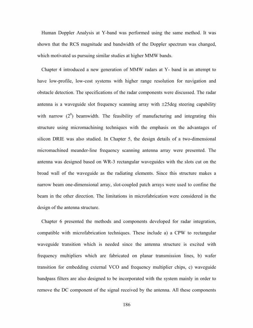
186
Human Doppler Analysis at Y-band was performed using the same method. It was
shown that the RCS magnitude and bandwidth of the Doppler spectrum was changed,
which motivated us pursuing similar studies at higher MMW bands.
Chapter 4 introduced a new generation of MMW radars at Y- band in an attempt to
have low-profile, low-cost systems with higher range resolution for navigation and
obstacle detection. The specifications of the radar components were discussed. The radar
antenna is a waveguide slot frequency scanning array with 25deg steering capability
with narrow (20) beamwidth. The feasibility of manufacturing and integrating this
structure using micromachining techniques with the emphasis on the advantages of
silicon DRIE was also studied. In Chapter 5, the design details of a two-dimensional
micromachined meander-line frequency scanning antenna array were presented. The
antenna was designed based on WR-3 rectangular waveguides with the slots cut on the
broad wall of the waveguide as the radiating elements. Since this structure makes a
narrow beam one-dimensional array, slot-coupled patch arrays were used to confine the
beam in the other direction. The limitations in microfabrication were considered in the
design of the antenna structure.
Chapter 6 presented the methods and components developed for radar integration,
compatible with microfabrication techniques. These include a) a CPW to rectangular
waveguide transition which is needed since the antenna structure is excited with
frequency multipliers which are fabricated on planar transmission lines, b) wafer
transition for embedding external VCO and frequency multiplier chips, c) waveguide
bandpass filters are also designed to be incorporated with the system mainly in order to
remove the DC component of the signal received by the antenna. All these components
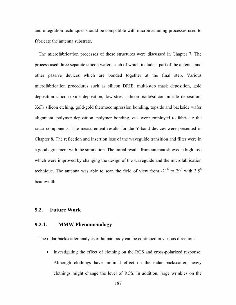
187
and integration techniques should be compatible with micromachining processes used to
fabricate the antenna substrate.
The microfabrication processes of these structures were discussed in Chapter 7. The
process used three separate silicon wafers each of which include a part of the antenna and
other passive devices which are bonded together at the final step. Various
microfabrication procedures such as silicon DRIE, multi-step mask deposition, gold
deposition silicon-oxide deposition, low-stress silicon-oxide/silicon nitride deposition,
XeF2 silicon etching, gold-gold thermocompression bonding, topside and backside wafer
alignment, polymer deposition, polymer bonding, etc. were employed to fabricate the
radar components. The measurement results for the Y-band devices were presented in
Chapter 8. The reflection and insertion loss of the waveguide transition and filter were in
a good agreement with the simulation. The initial results from antenna showed a high loss
which were improved by changing the design of the waveguide and the microfabrication
technique. The antenna was able to scan the field of view from -210 to 290 with 3.50
beamwidth.
9.2. Future Work
9.2.1. MMW Phenomenology
The radar backscatter analysis of human body can be continued in various directions:
Investigating the effect of clothing on the RCS and cross-polarized response:
Although clothings have minimal effect on the radar backscatter, heavy
clothings might change the level of RCS. In addition, large wrinkles on the
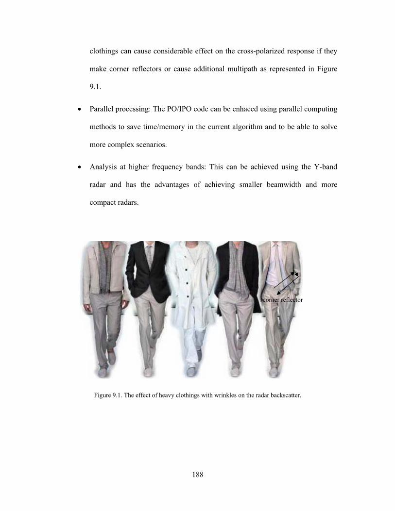
188
clothings can cause considerable effect on the cross-polarized response if they
make corner reflectors or cause additional multipath as represented in Figure
9.1.
Parallel processing: The PO/IPO code can be enhaced using parallel computing
methods to save time/memory in the current algorithm and to be able to solve
more complex scenarios.
Analysis at higher frequency bands: This can be achieved using the Y-band
radar and has the advantages of achieving smaller beamwidth and more
compact radars.
Figure 9.1. The effect of heavy clothings with wrinkles on the radar backscatter.
corner reflector

189
9.2.2. MMW Technology
The future work of this project mainly involves the integration of the Y-band radar.
This includes verification of the performance of the thru-wafer transition for packaging
and the hybrid-coupled patch arrays as well as the performance of the active components
of the radar. Moreover, the technologies empowered by the contribution of this work are
numerous. These include improvement in microfabrication processes and enhancing the
antenna performance.
9.2.2.a. Microfabrication Improvement
The performance of the radar antenna was enhanced using lower-loss waveguide
structure (with larger dimensions) and larger slot dimension. This could be further
optimized considering limitations in microfabrication such as the maximum achievable
etch depth and optimization of the parameters of gold thermocompression bonding such
as bonding pressure and temperature to maintain the quality. It was experimentally shown
that by using mask layers with high selectivity, the etch depth for the current process can
be as deep as 1 mm. Also, gold bonding can be performed in lower temperatures and
pressures by forfeiting the mechanical bonding quality. In addition, the non-uniform
etching of silicon caused by loading effect in DRIE can be completely compensated using
etch-stop layers. These layers are commonly thin high quality silicon oxide layers which
are very selective to DRIE and are very efficiently used as etch-stop.
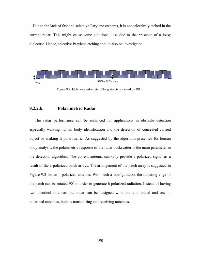
190
Due to the lack of fast and selective Parylene etchants, it is not selectively etched in the
current radar. This might cause some additional loss due to the presence of a lossy
dielectric. Hence, selective Parylene etching should also be investigated.
Figure 9.2. Etch non-uniformity of long structure caused by DRIE
9.2.2.b. Polarimetric Radar
The radar performance can be enhanced for applications in obstacle detection
especially walking human body identification and the detection of concealed carried
object by making it polarimetric. As suggested by the algorithm presented for human
body analysis, the polarimetric response of the radar backscatter is the main parameter in
the detection algorithm. The current antenna can only provide v-polarized signal as a
result of the v-polarized patch arrays. The arrangement of the patch array is suggested in
Figure 9.3 for an h-polarized antenna. With such a configuration, the radiating edge of
the patch can be rotated 900 in order to generate h-polarized radiation. Instead of having
two identical antennas, the radar can be designed with one v-polarized and one h-
polarized antennas, both as transmitting and receiving antennas.
hWG 80%~ 85% hWG

191
(a) (b) Figure 9.3. (a) v-polarized and (b) proposed feeding technique for h-polarized antennas for the same slot.
radiating edge

192
BIBLIOGRAPHY
[1] P. Bhartia and I. J. Bahl, Millimeter Wave Engineering and Applications, New York:
John Wiley, 1984.
[2] URL:http://www.rfcafe.com/references/electrical/ew-radar-handbook/rf-atmospheric-
absorption-ducting.htm
[3] H. J. Liebe, T. Manabe, G. A. Hufford. “Millimeter-wave attenuation and delay rates
due to fog/cloud conditions”, IEEE Trans. Antennas Propagat., vol. 37, pp. 1617–1623,
Dec. 1989.
[4] D. M. Sheen, D. L. McMakin, and T. E. Hall, “Three-dimensional millimeter-wave
imaging for concealed weapon detection,” IEEE Trans. Microwave Theory Tech., vol. 49,
pp.1581–1592, Sep. 2001.
[5] K. B. Cooper, R. J. Dengler, G. Chattopadhyay, E. Schlecht, J. Gill, A. Skalare, I.
Mehdi, and P. H. Siegel, “A high-resolution imaging radar at 580 GHz,” IEEE Microw.
Wireless Compon. Lett., vol. 18, no. 1, pp. 64–66, Jan. 2008.
[6] A. B. del Campo, A. A. Lopez, B. P. D. Naranjo, J. G. Menoyo, D. R. Moran, and C.
C. Duarte, “CWLFM millimeter-wave radar for ISAR imaging with range coverage,” in
Proc. IEEE Int. Radar Conf., May 9–12, 2005, pp. 933–938.
[7] H. D. Collins, D. L. McMakin, T. E. Hall, and R. P. Gribble, “Real-time holographic
surveillance system,” U.S. Patent 5 455 590, Oct. 3, 1995.

193
[8] R. W. McMillan, N. C. Currie, D. D. Ferris, and Jr. M. C. Wicks, “Concealed weapon
detection using microwave and millimeter wave sensors,” Microwave and Millimeter
Wave Technology Proceedings, pp. 1-4, 1998.
[9] V. B. Shteinshleinger, et. al., “A new type of device to locate objects hidden under
the clothes of people,” 2001 CIE International Conference on, Proceedings, pp. 227-230.
[10] R. W. McMillan, "Terahertz Imaging, Millimeter-Wave Radar," Advances in
Sensing with Security Applications Digest, NATO Advanced Study Institute, Il Ciocco,
Italy, pp. 1-26, July 17-30, 2005.
[11] Automatic two-stage IR and MMW image registration algorithm for concealed
weapons detection. Chen, H.-M. Varshney, P.K. Vision, IEE Proceedings Image and
Signal Processing, Aug 2001, vol. 148, number 4, pp 209-216.
[12] P. F. Goldsmith, C.-T. Hsieh, G. R. Huguenin, J. Kapitzky, and E. L. Moore.
“Focal Plane Imaging Systems for Millimeter Wavelengths”, IEEE Trans. Microwave
Theory and Techniques, Vol. 41, pp. 1664–1675, October 1993.
[13] T. Dogaru, C. Le, and G. Kirose, “Time-Frequency Analysis of a Moving Human
Doppler Signature,” Army research lab technical report, ARL-TR-4728, Feb 2009.
[14] W. H. Haydl, M. Neumann, L. Venveyen, A. Bangert, S. Kudszus, M.
Schlechtweg, A. Hulsmann, A. Tessmann, W. Reinert, and T. Krems, “Single-chip
coplanar 94-GHz FMCW radar sensors,” IEEE Microw. Guided Wave Lett., vol. 9, no. 2,
pp. 73–75, Feb. 1999.
[15] A. Tessmann, S. Kudszus, T. Feltgen, M. Riessle, C. Sklarczyk, and W. H. Haydl,
“Compact single-chip W-band FMCW radar modules for commercial high-resolution

194
sensor applications,” IEEE Trans. Microw. Theory Tech., vol. 50, no. 12, pp. 2995–3001,
Dec. 2002.
[16] I. D. Robertson and S. Lucyszyn , RFIC and MMIC Design and Technology, 1st
ed. The Institution of Electrical Engineers, London, 2001.
[17] G. D. Morgan, P. D. Beasley, C. L. Murray, and C. Koh, “Design considerations
for a millimetric front-end for FMCW radar,” in Inst. Eng. Technol. Millimeter-Wave
Products Technol. Seminar, Nov. 16, 2006, pp. 7–12.
[18] P. Uhlig, C. Günner, S. Holzwarth, J. Kassner, R. Kulke, A. Lauer, and M.
Rittweger, “LTCC short range radar sensor for automotive application at 24 GHz,” in
Proc. 37th Int. Microelectron. Symp., Nov. 14–18, 2004.
[19] C. Wang, R. Qian, and X.-W. Sun, “Low cost _-band FMCW radar modules for
automobile application,” in Proc. IEEE Int. RF Integration Technol.: Integrated Circuits
for Wideband Commun. Wireless Sensor Networks Workshop, Nov. 30–Dec. 2 2005, pp.
153–156.
[20] R. Kulke, C. Günner, S. Holzwarth, J. Kassner, A. Lauer,M. Rittweger, P. Uhlig,
and P. Weigand, “24 GHz radar sensor integrates patch antenna and frontend module in
single multilayer LTCC substrate,” in Eur. Microelectron. Packag. conf., Jun. 12–15,
2005, pp. 239–242.
[21] S. Raman and G. M. Rebeiz, “A 94 GHz unipolar subharmonic mixer,” in IEEE
MTT-S Int. Microwave Symp. Dig., vol. 1, Jun. 1996, pp. 385–388.
[22] H. F. Cook, “Dielectric Behavior of Some Types of Human Tissues at Microwave
Frequencies”, J. Appl. Phys., Vol. 2, pp. 295-300, 1951.

195
[23] C.M. Alabaster, ‘Permittivity of human skin in millimetre wave band,”
Electronics Lett. ,16th October 2003 Vol. 39 No. 21
[24] Walters, T., et. al, “Heating and pain sensation produced in human skin by
millimeter waves: comparison to a simple thermal model’, Health Physics, Mar. 2000,
78, 3, pp 259 – 267
[25] Gabriel, C. and Gabriel, S.: ‘Compilation of the dielectric properties of body
tissue at RF and microwave frequencies’, Final report for AFOSR/NL Bolling AFB DC
20332-0001, June 1996.
[26] URL: http://www.makehuman.org/
[27] K. M. Robinette, H. Daanen, and E. Paquet, “The CAESAR project: a 3-D surface
anthropometry survey,” in Proc. 3-D Digital Imaging and Modelling, pp. 380-386, Oct.,
1999, Ottawa, Canada
[28] URL: http://um3d.dc.umich.edu
[29] F. T. Ulaby, C. Elachi, Radar Polarimetry for Geoscience Applications. Artech
House, Norwood, MA, 1990.
[30] F. Obelleiro, M. G. Araujo, J. L. Rodriguez, “Iterative physical-optics formulation
for analyzing large waveguide with lossy walls,” Microwave Opt. Tech. Lett., vol. 28, pp.
21-26, Jan. 2001.
[31] T. Griesser and C. A. Balanis, “Dihedral corner reflector backscatter using higher
order reflections and diffractions,” IEEE Trans. Antennas Propagat., vol. 35, pp.1235-
1247 Nov. 1987.

196
[32] R. D. De Roo and F. T. Ulaby, “Bistatic specular scattering from rough dielectric
surfaces,” IEEE Trans. Antennas and Propagat., vol. 42, pp. 220-231, Feb. 1994
[33] Nashashibi A., Ulaby F., and Sarabandi K., “Measurement and modeling of the
millimeter wave backscatter response of soil surfaces,” IEEE Trans. Geosci. Remote
Sensing, vol. 34, no. 2, pp. 561-572, Jan. 1996
[34] P. van Dorp and F. C. A. Groen, “Human walking estimation with radar,” IEE
Proc. –Radar Sonar Navig., vol. 150, No. 5, Oct. 2003
[35] G. E. Smith, K. Woodbridge, and C. J. Baker, “Multistatic micro-doppler
signature of personnel,” IEEE Radar Conference, pp. 1–6, 2008.
[36] Y. Kim and H. Ling, “Human activity classification based on microdoppler
signatures using a support vector machine,” IEEE Trans. Geosci. Remote Sensing, vol.
47, no. 5, pp. 1328–1337, 2009.
[37] B. G. Mobasseri and M. Amin, “A time-frequency classifier for human gait
recognition,” in SPIE Defense, Security and Sensing, vol. 7306, 2009.
[38] C. Hornsteiner, and J. Detlefsen,“ Characterisation of human gait using a
continuous-wave radar at 24 GHz,” Advances in Radio Science 2008, Vol. 6, p. 67-70
[39] D. Polder and J. H. van Santen, “The effective permeability of mixtures of
solids,” Physica, vol. 12, no. 5, pp. 257-271, 1946.
[40] Helmut Essen, et. al. “A High Performance 220-GHz Broadband Experimental
Radar”, IRMMW-THz 2008, Pasadena, USA, September 2008.

197
[41] G.P. Gauthier, J.P. Raskin, and G.M. Rebeiz, A 140–170-GHz low-noise
uniplanar subharmonic Schottky receiver, IEEE Trans Microwave Theory Tech, vol. 48,
2000, 1416–1419.
[42] Abbasi, M., Gunnarsson, S.E., Wadefalk, N., Kozhuharov, R., Svedin,
J., Cherednichenko, S., Angelov, I., Kallfass, I., Leuther, A., Zirath, H., "Single-Chip
220-GHz Active Heterodyne Receiver and Transmitter MMICs With On-Chip Integrated
Antenna", IEEE Trans. Microwave Theory Tech, pp: 466 - 478, Volume: 59 Issue: 2,
Feb. 2011
[43] S. Gunnarsson , N. Wadefalk , J. Svedin , S. Cherednichenko , I. Angelov , H.
Zirath , I. Kallfass and A. Leuther "A 220 GHz single-chip receiver MMIC with
integrated antenna", IEEE Microw. Wireless Compon. Lett., vol. 18, no. 4, pp.284 -
286 , 2008.
[44] B. Pan, Y. Li, G.E. Ponchak, J. Papapolymerou, and M.M. Tentzeris, A 60-GHz
CPW-fed high-gain and broadband integrated horn antenna, IEEE Trans Antennas
Propagat 57 ( 2009), pp. 1050–1056.
[45] M. Jankiraman, Design of Multi-Frequency CW Radars, Scitech Publishing, Inc.,
2007.
[46] Skolnik, M. I. (ed.), Radar Handbook, McGraw-Hill (1970)
[47] W. Menzel, D. Pilz, and R. Leberer, “A 77-GHz FM/CW radar front-end with a
low-profile low-loss printed antenna,” IEEE Trans. Microw. Theory Tech., vol. 47, no.
12, pp. 2237–2241, Dec. 1999.

198
[48] M. E. Russell et al., “Millimeter-wave radar sensor for automotive intelligent
cruise control (ICC),” IEEE Trans. Microwave Theory Tech., vol. 45, pp. 2444–2453,
Dec. 1997.
[49] Y. Kimura, H. Shinoda, J. Hirokawa, and M. Ando, “Sidelobe suppression of two-
beam single-layer slotted waveguide array,” in Asia–Pacific Microwave Conf.,
Yokohama, Japan, 1998, pp. WE2D-1.
[50] T. Tanizaki et al., “Multi-beam automotive radar front end using noncontact
cylindrical NRD switch,” in IEEE Int. Microwave Symp. Dig., Baltimore, MD, 1998, pp.
521–524.
[51] K. L. Klohn, R. E. Horn, H. Jacobs, and E. Freibergs, “Silicon waveguide
frequency scanning linear array antenna,” IEEE Trans. Microwave Theory Tech., vol.
MTT-26, pp. 764–773, Oct. 1978.
[52] Manasson, et. al., "MMW scanning antenna," IEEE Aerospace and Electronic
Systems Magazine, vol. 11, no. 10, pp. 29-33, Oct. 1996
[53] V. Fusco, “Mechanical beam scanning reflect array,” IEEE Trans. Antennas
Propag., vol. 53, no. 11, pp. 3842–3844, Nov. 2005.
[54] Metamaterial based steerable antenna for millimeter wave radar applications
[55] K. V. Caekenberghe, T. Vaha-Heikkila, G. Rebeiz, and K. Sarabandi, “Ka-band
MEMS TTD passive electronically scanned array (ESA),” in Proc. IEEE APS/URSI
Symp., Albuquerque, NM, Jul. 2006, pp. 513–516.

199
[56] B. Schoenlinner, X. Wu, J. Ebling, G. Eleftheriades, and G. Rebeiz, “Wide-scan
spherical-lens antennas for automotive radars,” IEEE Trans. Microw. Theory Tech., vol.
50, no. 9, pp. 2166–2175, Sep. 2002.
[57] A. Ishimaru and H. S. Tuan, “Theory of frequency scanning antennas,” IRE
Trans. Antennas Propagat., vol. 10, Mar. 1962
[58] J. Bahl and K. C. Gupta, “Frequency scanning by leaky-wave antennas using
artificial dielectrics,“, IEEE lEEE TRANSACnONS ON A i i W A S k?4D
PROPAGATIoEi, JULY 1975 584-589
[59] H. Y. Yee, “The design of large waveguide arrays of shunt slots,” IEEE Trans.
Antennas Propag., vol. 40, pp. 775–781, 1992
[60] A. Patrovsky, and K. Wu, “Substrate integrated image guide array antenna for the
upper millimeter-wave spectrum,” IEEE Trans Antennas Propagat., vol. 55, pp. 2994-
3001, Nov. 2007.
[61] URL: http://www.qudostechnology.co.uk/etching.php
[62] URL: http://memscyclopedia.org/su8.html
[63] S. W. Yoon, V. P. Ganesh, et. al., “Packaging and assembly of 3-D silicon
stacked module for image sensor application,” IEEE Trans. Advanced Packaging, vol.
31, pp. 519-526, Aug. 2008.
[64] J. W. Digby, et. al. “Fabrication and characterization of micromachined
rectangular waveguide components for use at millimeter-wave and terahertz frequencies,”
IEEE Trans. Microwave Theory Tech., vol. 48, pp. 1293–1302, Aug. 2000.

200
[65] C. E. Collins, et. al. “A new micro-machined millimeter-wave and terahertz
snaptogether rectangular waveguide technology,” IEEE Microw. Guided Wave Lett., vol.
9, pp. 63–65, Feb. 1999.
[66] J. L. Hesler, K. Jui, R. K. Dahlstrom, R. M.Weikle, T. W. Crowe, C. M. Mann,
and H. B. Wallace, “Analysis of an octagonal micromachined horn antenna for
submillimeter-wave applications,” IEEE Trans. Antennas Propagat., vol. 49, pp. 997–
1001, June 2001.
[67] W. R. McGrath, C. Walker, M. Yap, and Y.-C. Tai, “Silion micromachined
waveguides for millimeter-wave and submillimeter-wave frequencies,” IEEE Microw.
Guided Wave Lett., vol. 3, pp. 61–63, Mar. 1993.
[68] R. N. Simons and S. R. Taub, “New coplanar waveguide to rectangular
waveguide end launcher,” Electron. Lett., pp. 1138–1139, June 1992.
[69] URL: http://www.microchem.com/products/su_eight.htm
[70] L. Josefesson, “A waveguide transverse slot for array applications”, IEEE Trans.
Antennas Propagat., vol. 41, pp. 845-850, July 1993
[71] R. E. Collin, Foundations for Microwave Engineering. New York: McGraw-Hill,
1966.
[72] R. S. Elliott, Antenna Theory and Design, Englewood Cliffs, Prentice-Hall, 1981,
page 90
[73] F. P. Van Der Wilt and J. H. M. Strijbos, “A 40 GHz planar array antenna using
hybrid coupling,” Perspectives Radio Astron. Technol. Large Antenna Arrays, pp. 129–
134, 1999

201
[74] URL:https://www51.honeywell.com/sm/em/products-applications/
dielectrics/spin-on-glass.html?c=21
[75] F. J. Goebels and T. S. Fong, “Four independent beams from a single linear
array,” IEEE Trans. Antennas Propagat., vol. AP-13, pp. 683–691, Sept. 1965.
[76] M. Vahidpour, and K. Sarabandi, “Cavity-backed coplanar waveguide to
rectangular waveguide transition for micromachining applications,” IEEE Trans.
Microwave Theory Tech.,
[77] T. Q. HO and Y. Shih, “Spectral-domain analysis of E-plane waveguide to
microstrip transitions,” IEEE Trans. Microwave Theory Tech., vol. 37, pp. 388-392, Feb.
1989.
[78] Y. Lee, J. P. Becker, J. East, L. P. B. Katehi, “Fully micromachined finite-ground
coplanar line-to-waveguide transitions for w-band applications,” IEEE Trans. Microwave
Theory Tech., vol. 52, pp. 1001-1007, Mar. 2004
[79] Y. Li, B. Pan, M. M. Tentzeris and J. Papapolymerou, "A fully micromachined
W-band coplanar waveguide to rectangular waveguide transition", in Proc. of 2007
IEEE-IMS Symposium, Honolulu, Hi, June 2007
[80] Y. Li, B. Pan, C. Lugo, M. M. Tentzeris, and J. Papapolymerou, "Design and
characterization of a W-band micromachined cavity filter including a novel integrated
transition from CPW feeding lines," IEEE Trans. Microwave Theory Tech., vol. 55, pp.
2902-2910, Dec. 2007
[81] N. Marcuvitz, Waveguide Handbook, McGraw-Hill, New York, 1951, pp. 271-
273

202
[82] R. F. Harrington, Time-Harmonic Electromagnetic Fields, McGraw-Hill, New
York, 1961, pp. 177-179 and 425-428
[83] M. Moallem, J. East, and K. Sarabandi, “Optimally designed membrane-
supported grounded CPW structure for submillimeter-wave applications,” Int. Symp.
Antennas Propagat. Charleston, NC. 2009.
[84] J. P. Becker, Y. Lee, J. R. East, and L. P. B. Katehi, “A finite ground coplanar
line-to-silicon micromachined waveguide transition,” IEEE Trans. Microwave Theory
Tech., vol. 49, p. 2001, Oct. 2001.
[85] Y. Lee, J. P. Becker, J. East, L. P. B. Katehi, “Fully micromachined finite-ground
coplanar line-to-waveguide transitions for w-band applications,” IEEE Trans. Microwave
Theory Tech., vol. 52, pp. 1001-1007, Mar. 2004
[86] Y. Li, B. Pan, M. M. Tentzeris and J. Papapolymerou, "A fully micromachined
W-band coplanar waveguide to rectangular waveguide transition", in Proc. of 2007
IEEE-IMS Symposium, Honolulu, Hi, June 2007.
[87] URL: www.mnf.umich.edu/ToolDocs/doc00088.pdf
[88] Tsau, C.H. Spearing, S.M. Schmidt, M.A., “Characterization of wafer-level
thermocompression bonds”, Microelectromechanical Systems, Journal of , vol. 13, pp.
963 - 971, Dec. 2004.
[89] J. Wu, et al., "Study on the Gold-Gold Thermocompression Bonding for Wafer-
level Packaging," Advanced Materials Research Vols. 60-61, pp 325-329, 2009.
[90] Hensup Kim, Dissertation, An Integrated Electrostatic Peristaltic Micropump
with Active Microvalves, University of Michigan, 2006

203
[91] Measurements of Micromachined Waveguide Devices at WR-3 Band using a
T/R-T Module Based Network Analyzer
[92] W. H. Chow, A. Champion, and D. P. Steenson, “Measurements to 320 GHz of
millimetre-wave waveguide components made by high precision and economic
micro-machining techniques,” in Proc. 8th High Freq. Postgrad. Stud. Colloq., 2003,
pp. 90–93.
[93] C. H. Smith, A Sklavonuos, and N. S. Barker, “SU-8 Micromachining of
Millimeter and Submillimeter Waveguide Circuits,” IEEE MTT-S International
Microwave Symposium, Vol. 1-3, pp. 961-964, 2009.
[94] T. Skaik, Y. Wang, M. Ke, S. Qian, and M. Lancaster, “A Micromachined WR-3
Waveguide with Embedded Bends for Direct Flange Connections,” Proc. 40th
European Microwave Conference, Paris, Sep. 2010, pp. 1225-1228.
[95] T. Gaier, L. Samoska, C. Oleson, G. Boll, “On-Wafer Testing of Circuits Through
220 GHz,” Ultrafast Optics and Electronics Conference, Snowmass, CO, April, 1999.
OSA Trends in Optics and Photonics Series Vol. 28, pp. 20-26.
[96] On-Wafer Vector Network Analyzer Measurements in the 220-325 GHz
Frequency Band
[97] OML, Inc. URL: http://www.omlinc.com/
[98] Virginia Diodes, Inc. URL: http://vadiodes.com/