a media enhanced vector architecture for embedded memory systemscsl.stanford.edu › ~christos ›...
TRANSCRIPT

A Media-Enhanced Vector Architecturefor Embedded Memory Systems
Christoforos Kozyrakis
Report No. UCB/CSD-99-1059
July 1999
Computer Science Division (EECS)University of CaliforniaBerkeley, California 94720

A Media-Enhanced Vector Architecturefor Embedded Memory Systems
by Christoforos Kozyrakis
Research Project
Submitted to the Department of Electrical Engineering and Computer Sciences, Uni-versity of California at Berkeley, in partial satisfaction of the requirements for thedegree of Master of Science, Plan II.
Approval for the Report and Comprehensive Examination:
Committee:
Professor David A. PattersonResearch Advisor
(Date)
* * * * * * *
Professor Katherine YelickSecond Reader
(Date)
A Media-Enhanced Vector Architecturefor Embedded Memory Systems
Christoforos Kozyrakis
M.S. Report
Abstract
Next generation portable devices will require processors with both low energy consump-
tion and high performance for media functions. At the same time, modern CMOS technology
creates the need for highly scalable VLSI architectures. Conventional processor architec-
tures fail to meet these requirements. This paper presents the architecture of Vector IRAM
(VIRAM), a processor that combines vector processing with embedded DRAM technology.
Vector processing achieves high multimedia performance with simple hardware, while em-
bedded DRAM provides high memory bandwidth at low energy consumption. VIRAM pro-
vides flexible support for media data types, short vectors, and DSP features. The vector
pipeline is enhanced to hide DRAM latency without using caches. The peak performance is
3.2 GFLOPS (single precision) and maximum memory bandwidth is 25.6 GBytes/s. With a
target power consumption of 2 Watts for the vector pipeline and the memory system, VIRAM
supports 1.6 GFLOPS/Watt. For a set of representative media kernels, VIRAM sustains on
average 88% of its peak performance, outperforming conventional SIMD media extensions
and DSP processors by factors of 4.5 to 17. Using a clustered implementation approach,
the modular design can be scaled without complicating control logic. We demonstrate that
scaling the architecture leads to near linear application speedup. We also evaluate the ef-
fect of scaling the capacity and parallelism of the on-chip memory system to die area and
sustained performance.

Contents
1 Introduction 1
2 The Architecture 32.1 Vector Register File . . . . . . . . . . . . . . . . . . . . . . . . . . . . . . 32.2 Vector Functional Units . . . . . . . . . . . . . . . . . . . . . . . . . . . . 52.3 Vector Pipeline for Embedded DRAM . . . . . . . . . . . . . . . . . . . . 6
2.4 Instruction Chaining . . . . . . . . . . . . . . . . . . . . . . . . . . . . . 92.5 Support for Short Vectors . . . . . . . . . . . . . . . . . . . . . . . . . . . 102.6 Vector Unit Implementation . . . . . . . . . . . . . . . . . . . . . . . . . 102.7 Memory System . . . . . . . . . . . . . . . . . . . . . . . . . . . . . . . . 11
2.8 Memory Management and Exception Processing . . . . . . . . . . . . . . 132.9 Support for Speculative Vector Execution . . . . . . . . . . . . . . . . . . 142.10 Network Interface and I/O . . . . . . . . . . . . . . . . . . . . . . . . . . 15
3 Discussion 153.1 Support for Media Processing . . . . . . . . . . . . . . . . . . . . . . . . 153.2 Energy Efficiency . . . . . . . . . . . . . . . . . . . . . . . . . . . . . . . 17
3.3 Design Scalability . . . . . . . . . . . . . . . . . . . . . . . . . . . . . . . 18
4 Performance 194.1 Base System Performance . . . . . . . . . . . . . . . . . . . . . . . . . . 204.2 Scaled System Performance . . . . . . . . . . . . . . . . . . . . . . . . . 224.3 Memory System Scaling . . . . . . . . . . . . . . . . . . . . . . . . . . . 24
5 Related Work 27
6 Conclusions 29
References
Acknowledgments


1 Introduction
Over the past few years, technology drivers for microprocessors have changed significantly.High-end systems for technical and scientific applications used to direct the evolution ofprocessor architecture. Now, consumer-level systems drive technology, due to their largevolume and attendant profits. Within this environment, important application and technol-
ogy trends have evolved. Media processing – such as video processing, speech recognitionand 3D graphics – is increasing in importance and will soon dominate the processing cyclesconsumed in computer-based systems [11]. Unlike traditional applications, media kernelsare characterized by large amounts of data parallelism, tolerance to latency, demand for high
memory bandwidth, and, often, limited temporal locality [12].
At the same time, the popularity of portable electronics and mobile applications is shift-ing the system focus from the desktop computer to personal mobile computing devices [23].
These devices require processors with low energy consumption and a high degree of integra-tion (“system-on-a-chip”) to increase battery life and reduce size and cost. Providing morenatural human interfaces for these portable devices through speech and image recognitionwill require greater performance for media functions.
Current high-performance microprocessors based on superscalar and out-of-order exe-cution are poor matches for this new environment, as they have been optimized for appli-cations with complex control flow and small working sets. To extract irregular instruction-level parallelism (ILP) from sequential application code dynamically, they expend consid-
erable chip area on sophisticated control logic and speculation buffers, which adds to cost,design complexity, and power consumption. To reduce average memory latencies, they uselarge multilevel caches, often including an array of expensive and power-hungry off-chipSRAM memories. Although caches are effective for applications that exhibit locality, theyincrease memory latency and reduce effective memory bandwidth for codes that do not.
We expect these superscalar designs to scale poorly into future CMOS technologies. Thestructures used to support dynamic ILP scale super-linearly with issue width. Worse, manyof these structures require global interactions which could impact cycle time given that in-
terconnect delays will limit communication speeds across future chip designs. Although itmay be possible to pipeline and cluster logic to remove long wires, this will further increasedesign and compiler complexity for these designs.
This paper presents the architecture of the Vector IRAM (VIRAM) microprocessor.VIRAM provides high multimedia performance with low energy consumption by integrat-ing vector processing with embedded DRAM technology. Vector processing allows simple,energy-efficient hardware to provide rapid execution of multimedia kernels. By eliminating
off-chip memory accesses, embedded DRAM technology provides both high sequential and
1

random memory bandwidth to large working sets with low energy consumption. The com-
ponent count for the whole system is decreased by integrating the processor and the memoryon the same die.
The major innovations in VIRAM compared to previous vector architectures includeflexible and scalable support for multimedia data types, optimizations for short vectors, the
design of a high-bandwidth memory system based on embedded DRAM, and support forvirtual memory and software speculative vector execution. The vector pipeline is designedto hide the latency of DRAM accesses without a cache structure or the need for long vectors.VIRAM supports 3.2 GFLOPS (single-precision) peak performance and 25.6 GByte/s peakmemory bandwidth. For a set of representative media kernels, 88% of the peak performance
is sustained on the average. The target power consumption for the vector unit and the mem-ory system is 2 Watts, achieved by using the modest clock frequency of 200 MHz that allowsa 1.2 V power supply. The 1.6 GFLOPS/Watt provided by VIRAM enable computationalintensive applications like speech recognition to run on portable, battery-operated devices.
An alternative implementation could use a higher power supply and a 400 MHz clock fre-quency, a feasible target in 0.18�m CMOS technology, to double the peak and sustainedperformance.
The vector unit implementation is based on multiple identical (parallel) clusters, lead-
ing to a modular and highly scalable design. Scaling the number of clusters leads to nearlinear application speedup without the need for recompilation. To observe performance im-provements for applications with indexed or strided memory accesses, increasing the com-putational power of the vector unit must be accompanied by a proportional increase of theon-chip memory system performance. Memory system performance can be improved by
providing a large number of independent memory banks or with a smaller number of banks,each of them organized as a collection of sub-banks. Independent banks allow memory ac-cesses to be issued and executed in parallel, while sub-banks allow memory accesses tooverlap their execution. The use of sub-banks is of great importance for systems with re-
duced on-chip memory capacity, which usually employ a small number of banks for areaefficiency.
The remainder of this paper is organized as follows. Section 2 presents the microarchi-tecture of VIRAM, including the pipeline structure and the memory system. In Section 3,we discuss media processing and DSP support, energy consumption characteristics, and the
scaling properties of the design. Section 4 presents the performance of the base VIRAMdesign and three scaled designs for a set of important media kernels. We also discuss theeffect of scaling the memory system capacity and parallelism on die area and sustained per-formance. In Section 5, we discuss alternative or similar architectural approaches for media
processing or embedded systems.
2

2 The Architecture
VIRAM is a vector microprocessor for media processing with on-chip main memory. Fig-ure 1 presents the block diagram of VIRAM. It contains a scalar unit, a vector coprocessor,
and a network interface all connected via a memory controller to the on-chip memory sys-tem. It is being designed in a 0.18�m embedded DRAM technology with a target clock rateof 200 MHz. The relatively low clock rate for this technology allows the low 1.2 V powersupply, used to reduce energy and power consumption.
The scalar unit 1 is a two-way superscalar core that implements the MIPS-IV instruc-tion set [21]. It includes two integer datapaths, a decoupled floating-point unit, and a non-blocking load/store unit. The scalar unit includes two-way set-associative primary instruc-tion and data caches, each holding 16 KBytes. A general coprocessor interface is provided
to facilitate the exchange of instructions and data with a coprocessor.
The vector unit is attached to the scalar unit as a loosely-coupled coprocessor. It exe-cutes a set of instructions defined as an extension to the basic MIPS ISA [27] that implementa vector register architecture. Vector arithmetic instructions perform a set of identical opera-
tions on the elements of vector operands located in the vector register file. VIRAM providesinteger (fixed-point) and floating-point operations for 16-bit, 32-bit, and 64-bit data widths.The vector instruction set also defines operations on 8-bit integers, which are not imple-mented in order to reduce design complexity. Vector load and store instructions move data
between the register file and the multi-bank DRAM system. The instruction set also pro-vides vector editing instructions such as compress and expand, extract operations for high-speed reductions, and special instructions for memory management and exception handling.The number of elements processed by a vector instruction is specified by the vector lengthcontrol register and can be set to any value between zero and the maximum number of vector
elements in a register.
To enhance performance, the scalar and the vector unit do not operate in lock-step. Thevector unit includes instruction buffers that allow the scalar core to run ahead. The two unitsare synchronized on vector unit exceptions, when vector unit state is read by the scalar core,
and on explicit synchronization instructions.
2.1 Vector Register File
The vector register file has a capacity of 8 KBytes and contains 32 general-purpose vec-tor registers, each holding up to 32 64-bit elements. Vector registers can be subdivided tohold 64 32-bit elements or 128 16-bit elements. If an application has vectors that exceed
1The scalar unit is designed by Sandcraft Inc., Santa Clara, CA.
3

VAFU VAFU
Flag Registers
VFFU
VMFU VMFU
VFFU
I/ONI
SEND
InstructionCache
DataCache
ScalarCore
...
01
BANK
DRAM
7
...
BANK
DRAM
89
15
MEMORY SYSTEM
RCVNI
TRX
Vector Registers
VECTOR UNITSCALAR UNIT
Memory Interface
NETWORK INTERFACE
Figure 1: The Block diagram of VIRAM.
4
the length of a vector register, strip-mining must be used. The vector register file provides
operands for arithmetic operations, indices for indexed memory accesses and storage fortemporary vector results.
There are also 32 vector flag registers, each containing a single bit per vector element.Flag registers are used to support conditional (predicated) vector execution, vector excep-tion processing, and software vector speculation [2]. Almost all vector instructions are con-ditional on a flag register that specifies which elements are active in an operation. The flagregister file has a capacity of 512 Bytes.
Two scalar register files are included in the vector unit. The first one stores control in-formation used for exception handling, memory management, and I/O configuration. It also
holds the base addresses and stride values for vector memory accesses. The second oneholds scalar operands used with vector operations (vector-scalar form). Although the reg-isters in the scalar unit could be used to provide scalar operands to vector instructions andbase addresses for vector memory references, separate register files are necessary in orderto comply with the MIPS coprocessor interface specification [21]. The interface does not
allow vector coprocessor instructions to read registers in the scalar core, but provides spe-cial move instructions that exchange data between two scalar register files in the vector andscalar units. Hence, every vector-scalar operation requires two instructions: one coproces-sor move and one vector instruction. The scalar register file in the vector unit provides stor-
age for scalar operands so that the number of coprocessor move operations is minimized toone per scalar operand needed, instead of one per vector-scalar instruction issued.
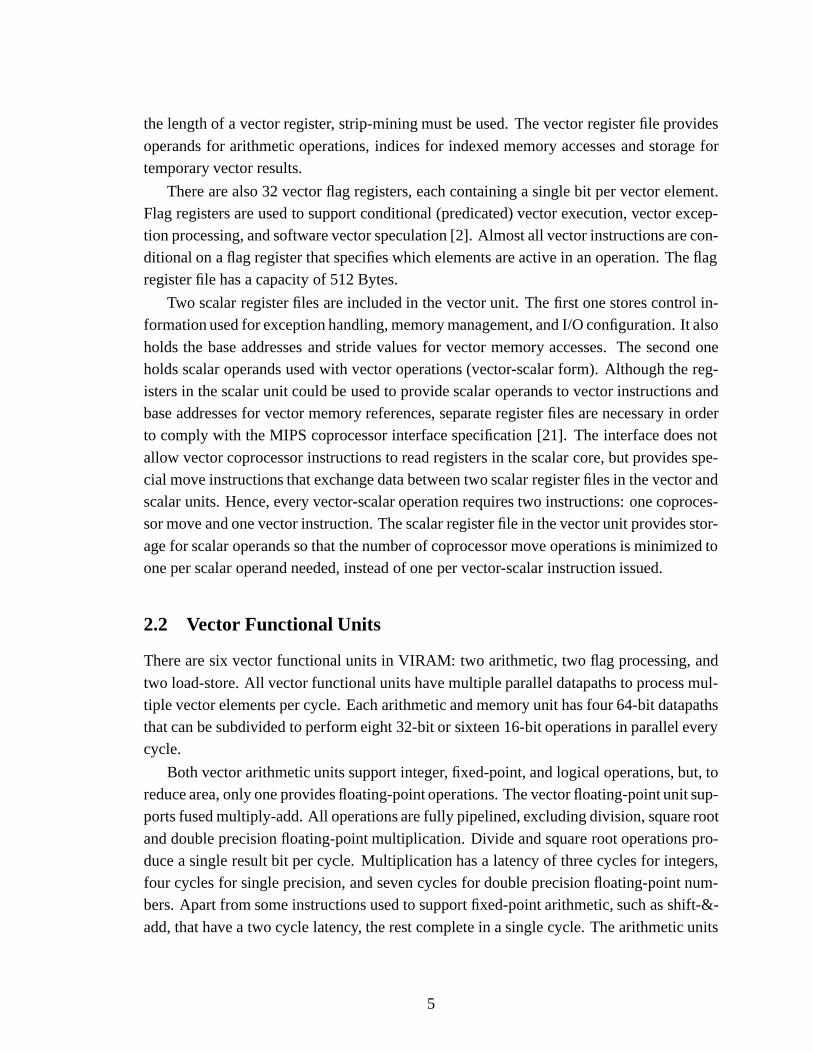
2.2 Vector Functional Units
There are six vector functional units in VIRAM: two arithmetic, two flag processing, and
two load-store. All vector functional units have multiple parallel datapaths to process mul-tiple vector elements per cycle. Each arithmetic and memory unit has four 64-bit datapathsthat can be subdivided to perform eight 32-bit or sixteen 16-bit operations in parallel everycycle.
Both vector arithmetic units support integer, fixed-point, and logical operations, but, toreduce area, only one provides floating-point operations. The vector floating-point unit sup-ports fused multiply-add. All operations are fully pipelined, excluding division, square root
and double precision floating-point multiplication. Divide and square root operations pro-duce a single result bit per cycle. Multiplication has a latency of three cycles for integers,four cycles for single precision, and seven cycles for double precision floating-point num-bers. Apart from some instructions used to support fixed-point arithmetic, such as shift-&-
add, that have a two cycle latency, the rest complete in a single cycle. The arithmetic units
5

also process vector extract operations used for fast reductions.
Flag processing units provide boolean operations on flag registers and also support pop-ulation count and priority encoding operations on flag vectors. Boolean operations on flagshave single cycle latency, while population count and priority encoding take two cycles. Allflag operations are fully pipelined.
The two load-store or memory units move data between the vector register file and the
memory system using one of three types of vector memory access: unit stride which ac-cesses contiguous memory locations, strided which accesses locations separated by a fixeddistance, and indexed which uses a vector register to provide pointers to memory (scatter-gather). Both memory units can perform unit stride operations, but only one can process
strided and indexed. A maximum of four independent addresses per cycle can be generatedfor a strided or indexed access references. Vector memory operations transfer 8, 16, 32 or64 bits per element. The only alignment restriction is that each element must be naturallyaligned. Each load-store unit exchanges up to 256 bits of data per cycle with the memorysystem.
Vector memory accesses are not cached, but hardware maintains coherence between thescalar cache and vector accesses. Coherence is achieved by generating invalidation requestsfor cached data written by the vector unit. The data cache also uses a write-through updatepolicy. To reduce the invalidation bandwidth requirements for the data cache, invalidation
requests are first filtered in the vector unit using replica of the data cache tags. Filteringeliminates invalidation requests for data not located in the data cache. Memory consistencybetween the scalar and vector units is maintained in software by using explicit synchroniza-tion instructions (memory barriers) and ordered vector stores [27]. Enforcing memory con-sistency in hardware would result in execution serialization and limit performance even for
applications that have no memory consistency problems.
2.3 Vector Pipeline for Embedded DRAM
The main memory of VIRAM is based on embedded DRAM, which has significantly dif-ferent performance characteristics than SRAM cache or SRAM main memory. An on-chipmulti-bank DRAM system can combine high capacity with main memory bandwidths onthe order of several tens of GBytes/s, but random access latency is at least 20 ns to 30 ns(4–6 processor cycles), even for the most aggressive embedded DRAM technology [10] 2.
The latency of the processor-DRAM interconnect further increases access latency. In addi-tion, DRAM has longer bank busy times than SRAM due to the potential need for restore,
2The random access latency for external DRAM is still considerably higher, typically between 100 ns and200 ns [31].
6
precharge and row access operations.
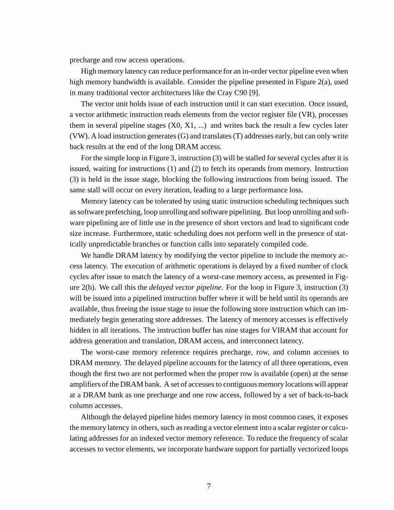
High memory latency can reduce performance for an in-order vector pipeline even whenhigh memory bandwidth is available. Consider the pipeline presented in Figure 2(a), used
in many traditional vector architectures like the Cray C90 [9].
The vector unit holds issue of each instruction until it can start execution. Once issued,a vector arithmetic instruction reads elements from the vector register file (VR), processes
them in several pipeline stages (X0, X1, ...) and writes back the result a few cycles later(VW). A load instruction generates (G) and translates (T) addresses early, but can only writeback results at the end of the long DRAM access.
For the simple loop in Figure 3, instruction (3) will be stalled for several cycles after it isissued, waiting for instructions (1) and (2) to fetch its operands from memory. Instruction(3) is held in the issue stage, blocking the following instructions from being issued. Thesame stall will occur on every iteration, leading to a large performance loss.
Memory latency can be tolerated by using static instruction scheduling techniques suchas software prefetching, loop unrolling and software pipelining. But loop unrolling and soft-
ware pipelining are of little use in the presence of short vectors and lead to significant codesize increase. Furthermore, static scheduling does not perform well in the presence of stat-ically unpredictable branches or function calls into separately compiled code.
We handle DRAM latency by modifying the vector pipeline to include the memory ac-cess latency. The execution of arithmetic operations is delayed by a fixed number of clockcycles after issue to match the latency of a worst-case memory access, as presented in Fig-ure 2(b). We call this the delayed vector pipeline. For the loop in Figure 3, instruction (3)
will be issued into a pipelined instruction buffer where it will be held until its operands areavailable, thus freeing the issue stage to issue the following store instruction which can im-mediately begin generating store addresses. The latency of memory accesses is effectivelyhidden in all iterations. The instruction buffer has nine stages for VIRAM that account foraddress generation and translation, DRAM access, and interconnect latency.
The worst-case memory reference requires precharge, row, and column accesses toDRAM memory. The delayed pipeline accounts for the latency of all three operations, even
though the first two are not performed when the proper row is available (open) at the senseamplifiers of the DRAM bank. A set of accesses to contiguous memory locations will appearat a DRAM bank as one precharge and one row access, followed by a set of back-to-backcolumn accesses.
Although the delayed pipeline hides memory latency in most common cases, it exposesthe memory latency in others, such as reading a vector element into a scalar register or calcu-lating addresses for an indexed vector memory reference. To reduce the frequency of scalar
accesses to vector elements, we incorporate hardware support for partially vectorized loops
7

F
DRAM Latency
VLOAD
VSTORE
VR X0 XN... VWVADD
D X W
Load -> Add RAW Hazard
Scalar Unit PipelineM
T VRG
T VWG
(a)
DRAM Latency
VLOAD
VSTORE
VR X0 ... VWXN
T VR
Delay Pipeline
XD M WF
VADD
Scalar Unit Pipeline
T VW
G
G
(b)
Figure 2: Vector pipeline models.
8

for (i=0; i<N; i+=VectorLength) f
(1) vector load reg1, addrA
(2) vector load reg2, addrB
(3) vector add reg3, reg1, reg2
(4) vector store reg3, addrC
g
Figure 3: Simple example of application kernel.
including compress, expand, and vector extract operations, and support for software vector
speculation. For the other cases, we rely on software instruction scheduling to minimize theimpact of the memory latency.
An interesting trade-off in the design of the delayed pipeline is the alignment of the read
stage (VR) in the pipeline for arithmetic and store operations and the write stage (VW) inthe pipeline for load operations. If these stages are aligned, as shown in Figure 2(b), anarithmetic operation issued a cycle after a load operation can use the loaded data withoutexperiencing any stalls. On the other hand, executing the vector register file earlier in the
pipeline for arithmetic and load instructions leads to smaller bank busy time for store op-erations and reduces the cost of moving the result of a vector arithmetic instruction to thescalar unit. Since for most multimedia applications it is easy to schedule load operationsseveral cycles before the arithmetic instructions that use their results, arithmetic and storeoperations in VIRAM read the vector register file three pipeline stages prior to the point that
load operations write the register file.The memory latency could also be hidden with a decoupled vector pipeline [14], which
also tolerates large variability in access latency. The delayed pipeline was preferred becauseit has simpler control, it does not require large hardware data buffers, and because there islittle latency variation in VIRAM. The decoupled pipeline should also have increased en-ergy consumption, because it has to write and read a data buffer on every memory reference.For the specific architecture and memory system of VIRAM, the data buffer needed for the
decoupled pipeline would be a four-ported 8 KByte SRAM block. This is comparable to thesize and design complexity of the vector register file. Section 4 presents performance resultsthat demonstrate the effectiveness of the delayed pipeline for multimedia applications.
2.4 Instruction Chaining
The vector unit is fully interlocked, meaning the hardware generates stalls to preserve de-pendencies on vector registers. Chaining, the extension of forwarding to vector architec-
tures [22], allows overlapping the execution of dependent instructions. The second instruc-
9
tion is allowed to access earlier element positions concurrently with the first instruction’s
access to later element positions in the same vector register. VIRAM supports chaining onall three types of hazards: RAW, WAR and WAW. Although the case of chaining RAW haz-ards is the most common and critical for performance, WAR chaining reduces pressure onvector register usage and WAW chaining accelerates applications with multiple concurrentconditional updates on the same register (vectorized if-then-else statements).
Chaining is implemented within the vector register file. The new value of any elementcan be read on the same cycle it is written. Additional bypass paths in the functional unitscould reduce the chaining latency by one cycle but would increase control complexity, diearea, and energy consumption.
2.5 Support for Short Vectors
We have optimized VIRAM’s performance for the case of short vectors to increase the rangeof applications that achieve speedups through vectorization. Unlike with many vector su-percomputers, the startup of all vector instructions is fully pipelined. There is no dead time
between instructions, and the vector pipelines can be saturated even with very short vectors.The delayed pipeline can tolerate long memory latency even with short vector lengths.
Post-incrementing addressing is supported for unit-stride and strided memory accessesto reduce the address manipulation overhead for short vectors. Due to limitations in the co-processor interface, incrementing a vector base address would otherwise require one scalar
addition and move instructions that would transfer the value in a base address register of thevector unit. The instruction bandwidth consumed for such operations would limit the per-formance in the case of short vectors, where each vector instruction has shorter completiontime and higher instruction bandwidth is required to keep the functional units busy.
Finally, VIRAM monitors the maximum vector length used by an application to reducethe overhead of saving and restoring state during a context switch. Only the vector register
elements actually used by the application need to be saved or restored on a context switch.
2.6 Vector Unit Implementation
The vector instruction set has been designed to support a clustered implementation of the
vector unit. Each hardware cluster, called a lane, includes one 64-bit datapath from eacharithmetic unit, part of the vector and flag register files, and two 64-bit ports to the memorysystem. The register files are partitioned so that each lane stores the register elements thatare processed by the local datapaths. The elements of a vector register are partitioned among
lanes in a round-robin fashion. All lanes are identical and are given the same control signals
10

on every cycle. VIRAM has four 64-bit lanes as shown in Figure 4. Each functional unit has
a total datapath width of 256 bits and spans across all lanes. Each lane includes eight 64-bitelements from every vector register and the corresponding masks from the flag register file.
There are several advantages to this implementation approach compared to a centralizedone. Communication between functional unit datapaths and the vector registers can be ac-commodated using local interconnect within each lane. The register file design is simplified,
as the bandwidth requirements are equally divided among four independent element parti-tions. Design complexity is reduced because a single lane design can be replicated. Vectorlanes are also important in scaling and improving the energy efficiency for this architecture.These issues are discussed in Section 3.
The register file partition in each lane still needs to sustain eight read and four write
operations for 64-bit elements per cycle. We split the SRAM block into two interleavedbanks [3] to halve the port requirements per bank. By performing all writes in the first halfof the clock cycle and all reads in the second, we require only four bit lines and four wordlines per storage cell. Register bank access conflicts have little performance impact for mostapplications [3].
2.7 Memory System
The basis of the memory system is the DRAM bank. Each bank can store 2 MBytes and has
a 256-bit synchronous interface3 with separate input and output signals. The interface is asimplified version of the SDRAM interface that supports a restricted set of operations suchas precharge, row access (activate), column access (256-bit read/write access). No burstaccess modes or auto-refresh is supported.
Bank accesses are pipelined and addresses can be received at the maximum rate of one
per clock cycle (5 ns). The DRAM cycle time for random read/write accesses is 20 ns. Peaksequential bandwidth per bank is 6.4 GBytes/s, while the worst case random bandwidth is1.6 Gbytes/sec. The memory system consists of eight to sixteen banks, leading to total ca-pacity of 16–32 MBytes, depending on our final die size. To simplify interconnect and toaddress manufacturing issues, banks are divided into two wings which are placed above and
below the scalar and vector units, as shown in Figure 5.
To connect the vector lanes and the memory banks, there are two pairs of crossbars, onepair per wing. Each pair includes separate load and store crossbars, both 256 bits wide.The data transferred may either be from contiguous memory locations or belong to four in-dependent 64-bit words from different DRAM banks. Each crossbar can deliver one to four
3The 2 MByte DRAM bank is designed by IBM. The bank is asynchronous and the synchronous interfaceis implemented in a “wrapper” logic block used to interface each macro to the rest of the system.
11

ElementsVector Register& DatapathsFlag Registers
Datapath 0Integer
Datapath 1Integer
Floating-pointDatapath
Memory Port 0
Memory Port 1
ElementsVector Register& DatapathsFlag Registers
Datapath 0Integer
Datapath 1Integer
Floating-pointDatapath
Memory Port 0
Memory Port 1
ElementsVector Register& DatapathsFlag Registers
Datapath 0Integer
Datapath 1Integer
Floating-pointDatapath
Memory Port 0
Memory Port 1
ElementsVector Register& DatapathsFlag Registers
Datapath 0Integer
Datapath 1Integer
Floating-pointDatapath
Memory Port 0
Memory Port 1
Lane 1 Lane 3Lane 2Lane 0
256 bits
64 bits
Figure 4: Clustering of functional unit datapaths and register file partitions into lanes.
I/O Scalar
Unit
Bank0
DRAM
Bank
DRAM
Bank
DRAM
Bank
DRAM
Bank
DRAM
Bank
DRAM
Bank
DRAM
Bank
DRAM
Bank
DRAM
Bank
DRAM
Bank
DRAM
Bank
DRAM
Bank
DRAM
Bank
DRAM
Bank
DRAM
Bank
DRAM
1 2 3 4 5 6 7
8 9 10 11
LaneLaneLaneLane
0 1 2 3
Crossbar Pair
Crossbar Pair
12 13 14 15
Figure 5: DRAM banks and vector lanes placement in VIRAM’s floorplan (drawing not toscale).
12

independent addresses per cycle to the banks of each wing. The combined peak bandwidth
of the crossbar structure is 25.6 GBytes/sec. Both memory units have equal access to eithermemory wing.
The scalar unit and the I/O interfaces communicate with memory by “stealing” cycleson the crossbar from the vector unit. As their bandwidth demands are relatively low, shar-ing does not create performance problems. The scalar core needs to access the memorysystem only on cache refills and write accesses. In addition, bandwidth intensive compu-tations on data with limited locality are typically handled in the vector unit. To reduce the
latency of cache refills, we allow accesses from the scalar core to “skip” the precharge androw access stages in the memory pipeline, if their data reside in open rows in the DRAMsystem. DRAM refresh accesses are periodically generated in the vector unit using a set ofrefresh counters. Refresh accesses also steal cycles from regular vector memory references
and have the higher priority from any other access type.
The support for multiple addresses in the memory system and including memory latencyin the vector unit pipeline structure allows VIRAM to sustain a large number of pending
accesses to memory with simple, pipelined hardware. Memory accesses for 72 64-bit ele-ments with up to 45 independent addresses may be in progress on any cycle. Such numbersare prohibitively expensive to support for other architectures.
2.8 Memory Management and Exception Processing
VIRAM provides full support for demand-paged virtual memory: a fully associative TLBwith 48 two-page entries caches virtual to physical address translations. The page sizessupported are 4, 16, 64, and 256 KBytes, and 1, 4, and 16 MBytes. There are two multi-ported micro-TLB structures to supply the necessary address translation bandwidth for vec-
tor memory accesses. The first one is two-ported – one port per load-store unit – and cachestranslations for unit stride accesses. The second one caches translations for strided and in-dexed accesses and has four ports, one per address generated for such accesses each clockcycle. The two micro-TLB structures have four single-page entries each and use least-
recently-used replacement (LRU) policy. Micro-TLB misses are handled in hardware withaccesses to the main TLB, while misses in the main TLB are handled by a software pagetable walk.
TLB miss exceptions and virtual memory exceptions are not precise, but they arerestartable. The vector unit postpones execution on such an exception in order to allowa software handler to observe its state and perform the proper exception processing tasks.When the exception has been served, the vector unit is allowed to continue execution at the
point it was interrupted. In the case of a context switch, vector unit state can be saved and
13

restored. The vector unit can be processing instructions for a different process than the one
running in the scalar unit. Therefore, periodical operating system handlers or processes thatdo not use the vector unit do not require saving or restoring vector unit state.
Vector arithmetic exceptions, both integer and floating-point, are not raised immediatelywhen the exceptional condition occurs. They are noted instead in dedicated flag registers[2], and an application can raise them by using trap barrier instructions. The flag registersprovide the information necessary for user-level handlers, such as exception type and the
vector elements that caused it.
2.9 Support for Speculative Vector Execution
Software speculative execution is supported to improve the scheduling of conditionally ex-ecuted vector statements by moving instructions above mask dependencies and branches in
the same way speculative execution is used to increase ILP for a superscalar processor bymoving instructions above control dependencies [2]. It is also used to allow vectorizationof loops with data dependent exit conditions. While hardware speculation relies solely onhardware to speculate dependencies and correct any mispredictions, in software speculativeexecution the hardware provides the necessary support for explicit speculation of dependen-
cies by the programmer or the compiler.
The VIRAM architecture supports software speculative execution by providing specu-lative versions of load operations and arithmetic instructions that may cause exceptions. Aspeculative vector load operation executes normally, but if there is an address error, zerois written in the proper vector element, and the corresponding mask is set in a dedicated
flag register for speculative load address errors. No address error exceptions are raised dur-ing the execution of a speculative load. A speculative vector arithmetic instruction exe-cutes normally as well, but writes exception flags into dedicated flag registers for specu-lative arithmetic exceptions. These flag registers are different from those used to note thearithmetic exceptions from regular, non-speculative, instructions.
To vectorize loops with data dependent exit conditions, one can use speculative instruc-
tions to execute loop iterations before the correct number of iterations is known 4. Whenthe exit condition is met, speculatively generated exceptions must be raised on discardedas appropriate. The hardware provides an instruction that raises speculative load addresserrors and merges the speculative arithmetic exception flags with those for non-speculativeinstructions for the vector elements that correspond to iterations that were correctly exe-
4Because no speculative store instruction is supported, speculative results should be kept in registers.Memory should be updated only when the speculation has been resolved, and the correct number of iterationsis known.
14

cuted. The flags for the remaining elements are discarded.
2.10 Network Interface and I/O
While VIRAM’s main application area is portable multimedia systems, support for parallelsystems is also provided. The network interface allows message-passing over four bidirec-tional links, each capable of a 100 MByte/s transfer rate in each direction. VIRAM chips
can be connected with these links to create parallel systems of arbitrary topology. They alsoallow a VIRAM chip to be used along with a hard disk drive as the building block for scal-able data servers like ISTORE [7].
The structure of the network interface is similar to those in the Alewife [24] and Fugu[26] systems. It is memory-mapped as a virtual resource and allows applications to sendshort or long messages without invoking the operating system. Short messages can be cre-ated by storing data directly into a message buffer in the network interface. For long mes-
sages, one or more DMA descriptors must be placed in the same buffer. A DMA engine willreplace each descriptor with the appropriate memory blocks before the message is trans-mitted over a communication link. The DMA engines for sending and receiving messagesin memory use virtual addresses. Both polling and user-level interrupt based message re-ception is supported. Protection is provided by bounding the duration of interrupt disable
periods and user-level exception handlers.
VIRAM also includes a system and a debugging interface. The system bus follows the
basic SysAD protocol for MIPS processors [20], extended to support split transactions. Itspeak bandwidth is 800 MBytes/s and it can be used to connect to various peripheral devicesand external DRAM. A separate DMA engine is available for data exchange over the systeminterface.
3 Discussion
3.1 Support for Media Processing
The vector processing model is a good match for multimedia applications, since most mediakernels process arrays or streams of pixels or samples in a SIMD fashion [12][13]. VIRAMoffers additional support for media processing by providing operations on the narrow datatypes frequently used in such applications and by implementing several features of digital
signal processors (DSP).
The data width of the vector unit can be changed to either 16-bit, 32-bit, or 64-bit by
writing to a control register. The narrower data widths allow more elements to be stored
15
* RightShift Round
+ SaturateX
Y
Zn/2
n/2
n
n
shiftamount
W
Vector Multiply Vector Shift - & - Add
n
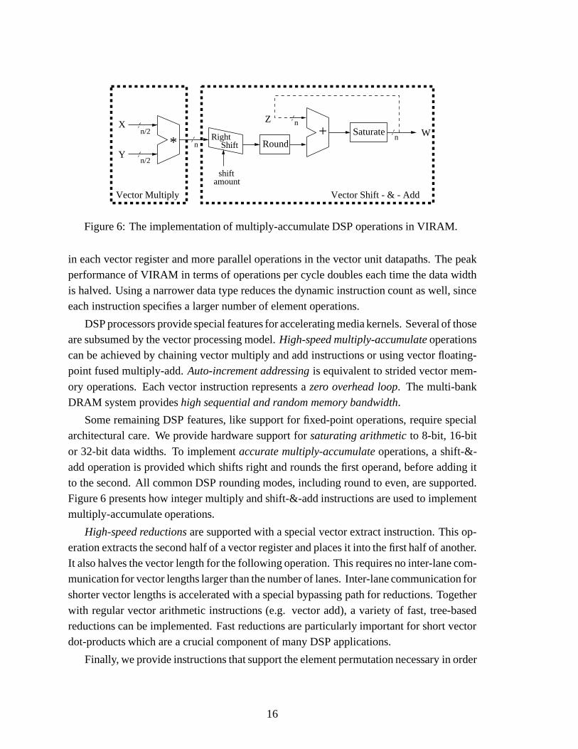
Figure 6: The implementation of multiply-accumulate DSP operations in VIRAM.
in each vector register and more parallel operations in the vector unit datapaths. The peakperformance of VIRAM in terms of operations per cycle doubles each time the data widthis halved. Using a narrower data type reduces the dynamic instruction count as well, sinceeach instruction specifies a larger number of element operations.
DSP processors provide special features for accelerating media kernels. Several of thoseare subsumed by the vector processing model. High-speed multiply-accumulate operationscan be achieved by chaining vector multiply and add instructions or using vector floating-point fused multiply-add. Auto-increment addressing is equivalent to strided vector mem-
ory operations. Each vector instruction represents a zero overhead loop. The multi-bankDRAM system provides high sequential and random memory bandwidth.
Some remaining DSP features, like support for fixed-point operations, require specialarchitectural care. We provide hardware support for saturating arithmetic to 8-bit, 16-bit
or 32-bit data widths. To implement accurate multiply-accumulate operations, a shift-&-add operation is provided which shifts right and rounds the first operand, before adding itto the second. All common DSP rounding modes, including round to even, are supported.Figure 6 presents how integer multiply and shift-&-add instructions are used to implementmultiply-accumulate operations.
High-speed reductions are supported with a special vector extract instruction. This op-eration extracts the second half of a vector register and places it into the first half of another.It also halves the vector length for the following operation. This requires no inter-lane com-munication for vector lengths larger than the number of lanes. Inter-lane communication for
shorter vector lengths is accelerated with a special bypassing path for reductions. Togetherwith regular vector arithmetic instructions (e.g. vector add), a variety of fast, tree-basedreductions can be implemented. Fast reductions are particularly important for short vectordot-products which are a crucial component of many DSP applications.
Finally, we provide instructions that support the element permutation necessary in order
16
to perform one step of a butterfly exchange on a vector register. These instructions utilize
the same hardware resources used for implementing fast reductions and provide significantspeedup for applications like FFT. They can also be used to synthesize multiple short vectorsinto a longer one.
3.2 Energy Efficiency
Low energy consumption is important for embedded microprocessors, particularly in
portable, battery-operated devices. Vector architectures have several inherent features thatlead to lower energy requirements compared to other high-performance architectures suchas superscalar and VLIW.
Instruction fetch, decode, and dispatch is performed once for a vector of operations,significantly reducing control logic energy requirements. Vector instructions provide the
hardware with explicit dependence information about element operations, hence no com-plex speculation, prediction, or re-order structure is needed to discover parallelism. Vectorinstructions also naturally partition operations among vector lanes, with mostly local com-munication within the lanes, thereby reducing interconnect energy.
By accessing main memory directly, no energy is wasted in caching data that has only
spatial locality, as is common in data-streaming media applications. Vector instructions alsoaccess memory and vector register banks in a regular pattern which avoids energy consump-tion in bank arbitration circuitry and enables power optimizations such as selective bankactivation.
Because vectors support highly parallel execution with low overhead, we can employvoltage scaling to reduce energy per operation [6]. By doubling the number of vector lanes,clock frequency can be halved without affecting the peak performance in terms of opera-tions per cycle. Lowering the clock frequency allows a proportional decrease in the powersupply voltage. Energy consumption is proportional to C �V 2
dd, where C is the total capaci-
tance being charged/discharged and Vdd is the power supply voltage. Even though datapathand control capacitance (C) can be doubled (worst-case) by increasing the number of lanes,the square factor of Vdd leads to reduced energy consumption for the same performance. Wedesign VIRAM to run at 200 MHz with a 1.2 V power supply and a target power consump-
tion of 2 W for the vector unit and the memory system.
Conditional execution provides another opportunity for reducing energy consumptionby controlling circuit activation and clock gating at a fine granularity. By reading the maskregister early in the pipeline, we can disable datapaths corresponding to masked-off elementoperations.
A final source of energy efficiency in VIRAM is the on-chip main memory. By elimi-
17
nating the need to drive off-chip, high capacitance buses for memory references, the energy
consumed in the memory system can be reduced by as much as a factor of four [16]. Theenergy consumption of the memory system is also reduced by using low-swing interconnecttechnology [41] in the design of the memory crossbar.
Despite the modest clock rate, the highly parallel design of VIRAM can support3.2 GOPS (32-bit operations) or 1.6 GOPS/Watt. StrongArm SA-110 [28], the leading mi-croprocessor in power/performance efficiency, achieves 0.11 GOPS/Watt, when clocked at200 MHz with a 2.2 V power supply. SA-110 was designed in a 0.35 �m CMOS process,
its peak performance for 32-bit integer multiply-add operations is 0.1 GOPS, and its typi-cal power consumption is 0.895 Watts. The next generation StrongArm processor [40], de-signed in a 0.18 �m process at 600 MHz with a 1.3 V power supply, is expected to support0.6 GOPS/Watt. VIRAM, an academic research project, outperforms both generations of
StrongArm in terms of power/performance efficiency by factors of 2.6 to 14.5.
3.3 Design Scalability
Scalability is an important consideration for processor architectures as transistor budgets,the speed of integrated circuits and requirements for performance improvements increase
according to Moore’s law. There are two equally important sides to scaling an architecture:scaling performance and scaling design complexity. Vector architectures have several ad-vantages when we consider future scaling of the design, both in terms of performance anddesign complexity.
Conventional architectures scale performance by increasing the operation frequency andthe number of arithmetic units in the design. The simplicity of vector unit hardware (simpleissue logic, increased locality within a lane) makes it easy to scale clock frequency. Still,
this may not be the most appropriate method for a energy-conscious design. Allocating ad-ditional arithmetic units allows the execution of more vector instructions in parallel. Onewould probably add memory units as well to keep the design balanced. However, each extrafunctional unit requires additional vector register file ports which increases design complex-
ity.
Vector performance can be readily scaled up by adding parallel lanes, or scaled down byremoving lanes. This performance scaling can be made transparent to compiled code. The
balance between arithmetic and functional units is maintained when scaling the number oflanes, as each lane contains both arithmetic datapaths and memory ports. Vector lengthslarger than the number of lanes are required to observe significant application speedup. Formany image processing kernels, the maximum application vector length is equal to the width
of an image or frame, typically in the order of hundreds of elements. Therefore, the number
18

of lanes in VIRAM can be doubled a few times and still lead to proportional improvements
in application performance.Vector architectures are also capable of scaling into future fabrication technologies
which will be much more sensitive to interconnect delays. The majority of communica-tion in the vector unit is held local to each lane, hence cycle time should not be affectedwhen scaling up the number of lanes. Vector performance is largely insensitive to vector
instruction broadcast latency which can be pipelined across the lanes. The memory cross-bar and the inter-lane networks to support extraction operations represent the main placeswhere wire-delay scaling will be visible in future technologies. Since vector architecturescan tolerate latency if sufficient fine-grain parallelism is available [2], the interconnect can
be pipelined to reduce the effects of wire delay scaling. Instruction chaining can be used tolimit the effect of the extra latency to one occurrence per application kernel or loop.
The memory system can be scaled by allocating additional DRAM banks, increasing thisway both memory capacity and bandwidth. The performance of the memory system can beimproved without increasing the overall capacity by modifying the DRAM bank interface.
To reduce access latency, each bank is organized as set of sub-banks connected through a busto a shared interface. Exposing the existence of sub-banks through the bank interface allowsaccesses to different sub-banks in the same bank to overlap. Effective memory bandwidthis therefore increased. Such accesses would otherwise lead to a bank conflict and would be
serialized.The rapidly increasing complexity of superscalar processor design [19][35] is a disad-
vantage when considering utilizing future high density fabrication processes. In contrast,VIRAM has a modular design both in the vector unit and memory system that can be read-ily scaled to larger designs. Control logic complexity grows only slowly with system size
whereas the design complexity of a superscalar, out-of-order design is a super-linear func-tion of issue width.
4 Performance
Table 1 presents the peak performance for arithmetic operations for the various integer andfloating-point data types supported in the vector unit. These numbers do not include theprocessing power of the scalar core. In general, peak performance doubles when data width
is halved. Peak floating-point performance depends on whether fused multiply-add can beutilized by the application. Double precision floating-point performance for multiply andmultiply-add operations is lower than that for additions, because multiplication is not fullypipelined for this data type.
We used a detailed performance model for our architecture to measure the sustained per-
19

Data Type Data Width Peak Performance
Integer 16b 6.4 GOPS32b 3.2 GOPS64b 1.6 GOPS
Floating-point 32b 3.2 GFLOPS(multiply-add) 64b 0.8 GFLOPS
Floating-point 32b 1.6 GFLOPS(multiply) 64b 0.4 GFLOPS
Floating-point 32b 1.6 GFLOPS
(add) 64b 0.8 GFLOPS
Table 1: The peak performance of VIRAM.
formance of VIRAM for a set of media kernels. The model simulates the vector unit andthe memory system in a cycle accurate fashion, excluding minor details such as DRAMrefresh cycles. We used the following set of representative media kernels: image composi-tion, iDCT, color conversion, convolution, and matrix-vector multiplication. Composition
or alpha blending merges two 8-bit single channel images using a weight factor. iDCT per-forms the 2D inverse discrete cosine transform on 8x8 blocks of 8-bit single channel im-ages using the AAN algorithm [1]. Color space conversion translates 24-bit RGB imagesto a YUV representation. Convolution applies a 3x3 box filter on an image. Finally, we im-plemented matrix-vector (V xM ) and vector-matrix (V TxM ) multiplication both for integer
and floating-point numbers. The matrix size used was 1000x1000. The kernels were codeddirectly in assembly and scheduled manually. Software pipelining was used for image com-position, color conversion, and convolution. For iDCT and matrix-vector multiplication,loop unrolling was also used.
4.1 Base System Performance
Table 2 presents the sustained performance of VIRAM for each kernel in terms of GOPS orGFLOPS and percentage of peak performance. The type and width of arithmetic operations
for each kernel are also listed. A memory system with sixteen DRAM banks (32 MBytes)was used. Sustained performance ranges from 48.5% to 100% of the peak with an averageof 88.8%. VIRAM efficiently exploits the data parallelism available in these applications,and DRAM latency is hidden by the delayed pipeline. For iDCT, performance is limited by
the large number of bank conflicts and the restriction of four addresses per cycle for strided
20

Kernel Data Type GOPS or GFLOPS % of Peak
Composition Int (16b) 6.40 100.0%
iDCT Int (16b) 3.10 48.5%
Color Conversion Int (32b) 3.07 96.0%
Convolution Int (32b) 3.16 98.7%
MxV Multiply Int (32b) 2.77 86.5%
VTxM Multiply Int (32b) 3.00 93.7%
MxV Multiply FP (32b) 2.80 87.5%
VTxM Multiply FP (32b) 3.19 99.6%
Average 88.8%
Table 2: The sustained performance of VIRAM for the media kernels.
VIRAM MMX [8] VIS [33] TMS320C82 [18]
Composition 0.13 - 2.22 (17.0x) -
iDCT 0.75 3.75 (5.0x) - 5.70 (7.6x)
Color Conversion 0.77 8.00 (10.4x) - -
Convolution 1.21 5.49 (4.5x) 6.19 (5.1x) 6.5 (5.3x)
Table 3: Performance comparison between VIRAM, MMX, VIS, and TMS320C82. Allnumbers are in cycles per pixel. The values in parentheses are the ratios of VIRAM’s per-
formance to that of the corresponding architecture. Ratios greater than 1.0 indicate higherperformance for VIRAM.
accesses 5. For matrix-vector multiplication, the MxV form is limited by the use of extract
operations for implementing reductions. These operations execute in one of the arithmeticunits but are not included in the arithmetic operation count for the kernel. The rest of thekernels achieve operations throughput within a few percentage points from the peak.
To compare with other architectures, we present performance in terms of cycles perpixel. Table 3 compares VIRAM to two general purpose architectures with SIMD exten-
sions and one DSP processor. MMX [29] and VIS [38] are 64-bit SIMD media extensionsused with the Pentium and UltraSparc processors respectively. The performance results forMMX and VIS assume that all data is located in the primary cache 6. This is an optimistic
5For the 16-bit data type, an arithmetic instruction can process 16 vector elements per clock cycle, whilea strided or indexed access can only proceed at the rate of four elements per cycle.
6SRAM caches usually have access latency and bank busy time of one or two processor cycles.
21

Kernel 1 Lane System 2 Lane System 4 Lane System 8 Lane System
Composition 1.60 (100%) 3.20 (100%) 6.40 (100%) 10.24 (80%)
iDCT 0.96 (60%) 1.85 (58%) 3.10 (48%) 3.63 (27%)
Color Conversion 0.79 (99%) 1.56 (98%) 3.07 (96%) 5.90 (92%)
Convolution 0.8 (100%) 1.59 (99%) 3.16 (99%) 6.05 (95%)
MxV Multiply 0.73 (91%) 1.45 (91%) 2.77 (87%) 4.78 (75%)
VTxM Multiply 0.79 (99%) 1.55 (97%) 3.00 (94%) 5.8 (91%)
MxV Multiply 0.75 (94%) 1.48 (93%) 2.80 (88%) 4.91 (77%)
VTxM Multiply 0.79 (99%) 1.59 (99%) 3.19 (99%) 6.38 (99%)
Average Efficiency 92.1% 90.8% 88.8% 78.2%
Table 4: The Sustained performance for VIRAM configurations with one, two, four, andeight lanes. The values in parentheses are the achieved percentages of the peak performance
for the corresponding configuration.
assumption, especially in the case of streaming media applications where temporal data lo-cality is limited. TMS320C82 [18] combines a RISC core with two 32-bit DSP cores archi-tected for media processing. All three systems can perform multiple narrow operations on
wider datapaths in parallel. Despite accessing directly the DRAM main memory instead of aSRAM primary cache, VIRAM outperforms the SIMD extensions by factors of 4.5 to 17. Afactor of four results from the use of four 64-bit lanes, leading to datapaths four times widerthan those in MMX and VIS. The remaining improvement is due to the benefits from im-plementing a complete vector instruction set, such as support for vector memory references.
VIRAM outperforms TMS320C82 by factors of 5.3 and 7.5 for convolution and iDCT re-spectively, demonstrating that the architecture efficiently supports DSP processors features.
4.2 Scaled System Performance
To demonstrate the scaling properties of our architecture, we simulated three additionalVIRAM systems with one, two and eight lanes respectively. Scaling the number of lanesadds both datapaths and memory ports to the system. We also scale the number of addresses
per cycle generated for strided and indexed accesses, and the number of addresses that canbe transfered by each crossbar to match the number of lanes. The rest of the system is thesame as the four-lane VIRAM we have presented. The same executables were used with allfour configurations. Table 4 presents the sustained performance for each configuration and
Figure 7 shows the speedup over the single lane system. Excluding iDCT, the speedup is
22

Spe
edup
0
1
2
3
4
5
6
7
8
Composition ConvolutioniDCT VM INT (32b)MV INT (32b) MV FP (32b)Color Conversion
VM FP (32b)
1 Lane 2 Lanes 4 Lanes 8 Lanes
Figure 7: The speedup of four VIRAM configurations over the single lane system.
Spe
edup
0
1
2
3
4
5
6
7
8
1 Lane 2 Lanes 4 Lanes 8 Lanes
1 sub-bank 2 sub-banks 4 sub-banks 8 sub-bank
60% 60% 60% 60%
58% 58% 58%58%
39%
48%58%58%58%27%
50% 51%
Figure 8: The speedup for iDCT with four different DRAM bank designs, each with a dif-ferent number of sub-banks. The percentage of peak performance achieved for each con-figuration is presented above the speedup column.
near linear, which shows that increasing the number of lanes leads to proportional increasesin application performance without rescheduling and recompilation.
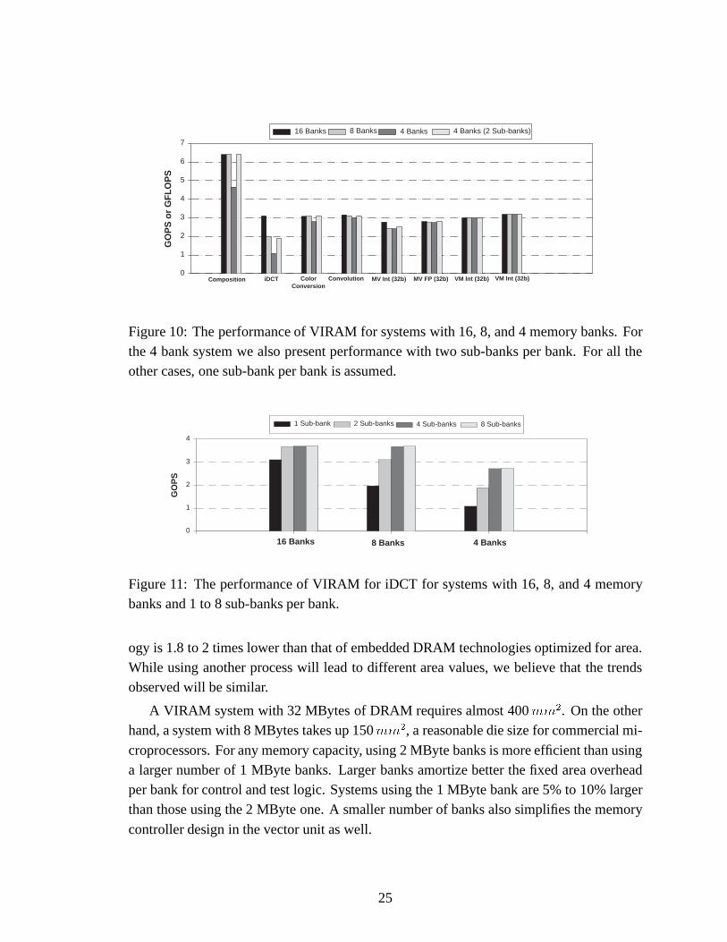
For iDCT, speedup is severely limited by bank conflicts in the memory system. As ex-plained in Section 2, conflicts can be reduced by modifying the DRAM bank interface toexpose the existence of sub-banks. Figure 8 shows the speedup for iDCT for systems withone, two, four and eight sub-banks per bank. Excluding the sub-banks, each configuration
is the same with the one described in the previous paragraph, and the same executable wasused. The system with four lanes and one sub-bank per bank is the one described in Section2. Four sub-banks provide sufficient parallelism in the memory system to achieve near lin-ear speedup and sustained performance between 50% and 60% of the peak. At this point,
the main performance bottleneck is the number of addresses generated per cycle for strided
23
8 MBytes 32 MBytes16 MBytes
Memory Capacity
Are
a (m
m2 )
0
50
100
150
200
250
300
350
400
450
Memory Area (1 MByte Banks)
Die Area (1 MByte Banks)
Memory Area (2 MByte Banks)
Die Area (2 MByte Banks)
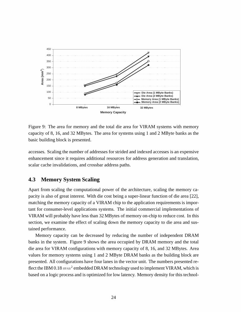
Figure 9: The area for memory and the total die area for VIRAM systems with memorycapacity of 8, 16, and 32 MBytes. The area for systems using 1 and 2 MByte banks as the
basic building block is presented.
accesses. Scaling the number of addresses for strided and indexed accesses is an expensive
enhancement since it requires additional resources for address generation and translation,scalar cache invalidations, and crossbar address paths.
4.3 Memory System Scaling
Apart from scaling the computational power of the architecture, scaling the memory ca-pacity is also of great interest. With die cost being a super-linear function of die area [22],matching the memory capacity of a VIRAM chip to the application requirements is impor-tant for consumer-level applications systems. The initial commercial implementations of
VIRAM will probably have less than 32 MBytes of memory on-chip to reduce cost. In thissection, we examine the effect of scaling down the memory capacity to die area and sus-tained performance.
Memory capacity can be decreased by reducing the number of independent DRAMbanks in the system. Figure 9 shows the area occupied by DRAM memory and the total
die area for VIRAM configurations with memory capacity of 8, 16, and 32 MBytes. Areavalues for memory systems using 1 and 2 MByte DRAM banks as the building block arepresented. All configurations have four lanes in the vector unit. The numbers presented re-flect the IBM 0.18mm2 embedded DRAM technology used to implement VIRAM, which is
based on a logic process and is optimized for low latency. Memory density for this technol-
24
GO
PS
or
GF
LOP
S
0
1
2
3
4
5
6
7
16 Banks 8 Banks 4 Banks 4 Banks (2 Sub-banks)
Composition iDCT ColorConversion
MV Int (32b)Convolution MV FP (32b) VM Int (32b)VM Int (32b)
Figure 10: The performance of VIRAM for systems with 16, 8, and 4 memory banks. Forthe 4 bank system we also present performance with two sub-banks per bank. For all theother cases, one sub-bank per bank is assumed.
GO
PS
0
1
2
3
4
1 Sub-bank 2 Sub-banks 4 Sub-banks 8 Sub-banks
16 Banks 4 Banks8 Banks
Figure 11: The performance of VIRAM for iDCT for systems with 16, 8, and 4 memorybanks and 1 to 8 sub-banks per bank.
ogy is 1.8 to 2 times lower than that of embedded DRAM technologies optimized for area.While using another process will lead to different area values, we believe that the trendsobserved will be similar.
A VIRAM system with 32 MBytes of DRAM requires almost 400mm2. On the otherhand, a system with 8 MBytes takes up 150mm2, a reasonable die size for commercial mi-
croprocessors. For any memory capacity, using 2 MByte banks is more efficient than usinga larger number of 1 MByte banks. Larger banks amortize better the fixed area overheadper bank for control and test logic. Systems using the 1 MByte bank are 5% to 10% largerthan those using the 2 MByte one. A smaller number of banks also simplifies the memory
controller design in the vector unit as well.
25

Number of Banks Bank Capacity Memory Capacity Memory Area Die Area(MBytes) (MBytes) (mm2) (mm2)
8 1.00 8 88.4 158.48 1.25 10 106.2 176.2
8 1.50 12 124.0 194.08 1.75 14 143.1 213.18 2.00 16 160.9 230.9
16 1.00 16 176.9 246.9
16 1.25 20 212.4 282.416 1.50 24 248.1 318.116 1.75 28 286.4 356.416 2.00 32 321.9 391.9
Table 5: The memory and die area for a four lane VIRAM system using DRAM banks with
capacity between 1 and 2 MBytes. Bank capacity is incremented by 0.25 MBytes. The areaof systems with 8 and 16 DRAM banks. is presented.
Figure 10 presents how scaling the number of banks affects the performance of a fourlane VIRAM system. By eliminating DRAM banks, the parallelism in the memory systemis reduced. Less addresses can be issued and processed in parallel, and it becomes more
difficult to hide DRAM bank busy time. Still, the performance for most kernels is not af-fected, even with the four bank system. For image composition, a kernel with three indepen-dent address streams, performance is significantly reduced with four banks due to the largenumber of memory conflicts 7. Exposing the existence of two sub-banks per bank is enough
to restore the original performance in this case. The use of sub-banks in systems with fewbanks is more critical for applications with strided or indexed accesses like iDCT. Figure 11presents the performance for iDCT as a function of the number of banks and sub-banks perbank. For the four bank system, eight sub-banks do not provide sufficient parallelism andperformance is 12% lower than that for the 16 bank system with one sub-banks per bank.
Multiple sub-banks allow accesses to the same bank to overlap, but they do not allow ac-cesses to be issued in parallel.
An alternative way to decrease memory capacity is scale the capacity of the DRAM
banks. Most embedded DRAM manufacturers provide a variety of DRAM banks sizes oreven compilers that can generate custom bank configurations. These banks usually differ in
7Most of these conflicts could be eliminated with intelligent memory allocation by an optimizing compilerthat is aware of the memory system structure.
26

Memory Capacity (MBytes)
8 10 12 14 16 18 20 22 24 26 28 30 32
Are
a (m
m2 )
0
50
100
150
200
250
300
350
400
450
Memory Area (16 Banks) Die Area (16 Banks)
Memory Area (8 Banks) Die Area (8 Banks)
Figure 12: The memory and die area for a four lane VIRAM system using DRAM bankswith capacity between 1 and 2 MBytes. Bank capacity is incremented by 0.25 MBytes. The
area of systems with 8 and 16 DRAM banks is presented.
the number DRAM rows they contain. Using banks with reduced capacity is less area effi-cient than reducing the number of (larger) banks, due to the area overhead for control and
test logic per bank. On the other hand, keeping the number of banks constant does not ef-fect the memory system parallelism and performance. The use of smaller banks also allowsscaling the memory capacity in late stages of the design process with minimal implicationsto the rest of the system. Table 5 and Figure 12 present the DRAM memory and die areafor VIRAM systems with 8 or 16 banks, where the bank capacity varies between 1 and 2
MBytes at increments of 0.25 MBytes. The total memory capacity of the system is between8 and 32 MBytes and die area varies between 160 and 390 mm2. Die area scales linearlywith memory capacity. Performance, on the other hand, is only affected by the number ofbanks in the memory system, not by bank capacity.
5 Related Work
Several other research efforts have focused on architectural enhancements for media-centricapplications. The majority of these systems are based on one of the following approaches:
VLIW, SIMD, reconfigurable logic, and stream processing.
27

VLIW systems, such as Trimedia [37] and VelociTI [39], exploit both regular and irreg-
ular parallelism at compile time. For vectorizable code running from a high latency mem-ory system, they require much greater instruction bandwidth and more sophisticated com-piler technology when scheduling loops in the presence of high memory latency. VLIW ma-chines must also adopt a clustered approach if they are to scale, which further complicatesthe compilation task. The compiler will be aware of both intra- and inter-cluster communi-
cation latencies. Increased code size is another disadvantage of VLIW systems.
SIMD extensions to existing processor architectures [29, 30] are essentially narrow vec-tor designs without support for vector memory operations. They have limited scalabilitybecause each instruction specifies a fixed number of operations. To utilize additional hard-
ware resources in the future, one has to either increase the superscalar issue width or modifythe instruction set to increase the width of SIMD operations. Most extensions do not sup-port SIMD memory operations, therefore exposing data alignment to user software [32].Certain instructions, such as random permutations, will not scale well due to interconnect
delay scalability problems. Recent simulation studies have demonstrated that, for mediaapplications, a two-way in-order superscalar processor with a vector unit can outperform afour-way out-of-order design with SIMD extensions by a factor of three [25].
Reconfigurable processors like PipeRench [17], based on FPGA technology, can pro-vide large speedups on some media applications. Reconfigurable systems excel at very nar-
row bit width operations but incur large die area and power consumption overheads whenimplementing wide arithmetic structures such as multipliers.
Imagine [34] is a stream processor which also relies on vector parallelism to reduce in-struction bandwidth and to cluster functional units. It has small register files local to each
functional unit backed up by a 64 KByte global stream register file. VIRAM has a vectorregister file distributed across lanes backed up by the on-chip memory. Whereas VIRAMprovides lanes with arbitrary random access to the larger on-chip memory, Imagine restrictsarithmetic clusters to access the stream register file using only sequential streams. Imagine
is an attached processor that has been designed to process long streams residing in a sepa-rate memory space from the host processor. In contrast, the VIRAM vector unit is tightlycoupled to the scalar unit sharing the same instruction stream and memory space, and it hasbeen designed to accelerate even short vector operations.
VIRAM is most similar to the T0 vector microprocessor [4] which was also targeted
towards multimedia. T0 had a much simpler SRAM memory system and lacked supportfor virtual memory, floating-point arithmetic, and partitionable datapaths. Other vector ma-chines include vector super-computers like the SGI/Cray SV1 [15] which have been op-timized for super-computer applications rather than low-energy embedded media applica-
tions.
28

Embedded DRAM processors, such as the M32R/D [36], are also available. These
merely integrate a simple RISC pipeline in an existing DRAM chip with limited enhance-ments for utilizing the increased memory bandwidth. In previous work, we have demon-strated the limited performance benefits of this approach [5]. The memory capacity of suchprocessors is usually limited to 4 MBytes, and the memory system organization is similarto that of traditional DRAM chips.
The architecture we present in this paper is targeted towards multimedia applicationsfor embedded, mobile systems. Its pipeline and memory system are designed for embeddedDRAM. Unlike other approaches, energy efficiency and scalability of both performance andphysical design are major points of focus.
6 Conclusions
Microprocessor architectures for next generation portable devices must provide both high-performance for media functions and reduced energy consumption. In addition, the scalingcharacteristics of CMOS technology require modular designs, that have mostly local inter-connect or can tolerate communication latency. Conventional microprocessors fail to meetthese requirements.
In this paper we presented VIRAM, a vector microprocessor with embedded mem-ory, optimized for multimedia applications. VIRAM addresses the requirements of futureportable devices by integrating vector processing and embedded DRAM. Vector processingprovides high performance for media functions with simple, scalable hardware, while em-bedded DRAM provides high memory capacity and bandwidth at low energy consumption.
Media processing is enhanced in VIRAM by providing flexible support for both narrowand wide data types and a set of DSP features like saturated arithmetic and fast reductions.The vector pipeline is optimized for short vectors and can tolerate high memory latency.Conditional execution, software vector speculation, and virtual memory are also supported.
The memory system consists of multiple synchronous DRAM banks interconnected witha high bandwidth crossbar structure. The vector unit design is modular. It is implementedusing multiple identical lanes, each one containing one datapath from every functional unit,two memory ports and a register file partition. Performance can be scaled by increasing thenumber of lanes without complicating control or issue logic. The highly parallel design can
provide high performance at low operational frequency and power supply, thus enablinghigh energy efficiency.
VIRAM is designed for 0.18�m technology with a 200 MHz clock frequency and 1.2V power supply. The target power consumption for the vector unit and the memory sys-
tem is 2 Watts. Peak performance is 6.4 GOPS (16-bit operations) or 3.2 GFLOPS (single-
29
precision). For a set of important media kernels, VIRAM achieves on average 88% perfor-
mance efficiency and outperforms DSP processors or architectures with SIMD media ex-tensions by factors of 4.5 to 17.
While the base design includes four lanes, we demonstrated that performance scales al-most linearly with the number of lanes in the system. For applications with indexed andstrided accesses, scaling the memory system performance in parallel with increasing the
computational power is necessary to observe performance benefits. Memory system per-formance can be improved by allocating more memory banks or exposing the existence ofsub-banks within each banks. Sub-banks are also important for improving the performanceof VIRAM systems with reduced memory capacity, which use a small number of banks for
area efficiency.Future work includes completing the physical design of VIRAM, and evaluating its
performance and energy characteristics using an actual demonstration system that includesVIRAM with several peripheral devices. The microprocessor presented in this paper is onepossible implementation of the VIRAM instruction set architecture. We intend to investi-
gate through simulations alternative organizations, both for the vector unit and the memorysystem. All architectural and implementation alternatives will be evaluated both for per-formance and energy efficiency. Some of the interesting issues are the number, mix, andcapabilities of functional units, the timing parameters of the memory system, and support
for density-time implementations of vector conditional execution.
30

References
[1] Y. Arai, T. Agui, and M. Nakajima. A Fast DCT-SQ Scheme for Images. Transactions of the
IEICE, E 71(11):1095, November 1988.
[2] K. Asanovic. Vector Microprocessors. PhD thesis, Computer Science Division, University of
California at Berkeley, 1998.
[3] K. Asanovic. VLSI Vector Register File Design. Submitted for Publication, December 1998.
[4] K. Asanovic, B. Kingsbury, B. Irissou, J. Beck, and J. Wawrzynek. T0: A Single-Chip Vec-
tor Microprocessor with Reconfigurable Pipelines. In The Proceedings of the 22nd European
Solid-State Circuits Conference, September 1996.
[5] W. Bowman, C. Cardwell, C. Kozyrakis, C. Romer, and H. Wang. Evaluation of Existing Ar-
chitectures in IRAM Systems. In The Workshop on Mixing Logic and DRAM, ISCA 24, June
1997.
[6] R.W. Brodersen, A. Chandrakasan, and S. Sheng. Design techniques for portable systems. In
The International Solid-State Circuits Conference, Digest of Technical Papers, pages 168–9,
February 1993.
[7] A. Brown, D. Oppenheimer, K. Keeton, R. Thomas, J. Kubiatowicz, and D. Patterson. IS-
TORE: Introspective Storage for Data-Intensive Network Services. In The Proceedings of the
7th Workshop on Hot Topics in Operating Systems (HotOS-VII), March 1999.
[8] Intel Corporation. MMX Technology Application Notes.
http://developer.intel.com/drg/mmx/appnotes/, 1996.
[9] Cray Research, Incorporated, Chippewa Falls, WI 54729. Cray Y-MP C90 System Programmer
Reference Manual, 001 edition, June 1993. CSM-0500-001.
[10] S. Crowder, R. Hannon, H. Ho, D. Sinitsky, S. Wu, K. Winstel, B. Khan, S. Stiffler, and S. Iye.
Integration of trench DRAM into a high-performance 0.18 �m logic technology with copper
BEOL. In The Proceedings of IEEE International Electron Devices Meeting, pages 1017–20,
December 1998.
[11] W. Dally. Tomorrow’s Computing Engines. Keynote Speech, Fourth International Symposium
on High-Performance Computer Architecture, February 1998.
[12] K. Diefendorff and P. Dubey. How Multimedia Workloads Will Change Processor Design.
IEEE Computer, 30(9):43–45, September 1997.
[13] P. Dubey. Architectural and Design Implications of Mediaprocessing. Tutorial, The Hot Chips
XI Symposium, August 1997.

[14] R. Espasa and M. Valero. Decoupled Vector Architecture. In The Proceedings of the Second
International Symposium on High-Performance Computer Architecture, February 1996.
[15] G. Faanes. A CMOS Vector Processor with a Custom Streaming Cache. In The Proceedings
of Hot Chips X Symposium, August 1998.
[16] R. Fromm, S. Perissakis, N. Cardwell, C. Kozyrakis, B. McGaughy, P. Patterson, T. Anderson,
and K. Yelick. The Energy Efficiency of IRAM Architectures. In The Proceedings of the 24th
Annual International Symposiumon Computer Architecture, June 1997.
[17] S. Goldstein, H Schmit, M. Moe, M. Budiu, S. Cadambi, R. Taylor, and R. Laufer. PipeRench:
a Coprocessor for Streaming Multimedia Acceleration. In The 26th International Symposium
on Computer Architecture, March 1999.
[18] J. Golston. Single-Chip H.324 Videoconferencing. IEEE Micro, 16(4):21–33, August 1993.
[19] G. Grohoski. Challenges and Trends in Processor Design: Reining in Complexity. IEEE Com-
puter, 31(1):41–42, January 1998.
[20] J. Heinrich. MIPS R4000 Microprocessor User Manual. MIPS Technologies Inc., 2nd edition,
1994.
[21] J. Heinrich. MIPS RISC Architecture, 2nd Edition. Silicon Graphics, Inc., 1998.
[22] J. Hennessy and D. Patterson. Computer Architecture: A Quantitative Approach, second edi-
tion. Morgan Kaufmann, 1996.
[23] C.E. Kozyrakis and D.A. Patterson. A New Direction in Computer Architecture Research.
IEEE Computer, 31(11):24–32, November 1998.
[24] J. Kubiatowicz and A. Agarwal. Anatomy of a Message in the Alewife Multiprocessor. In
Proceedings of the 7th ACM International Conference on Supercomputing, July 1993.
[25] C. Lee and M. Stoodley. Simple Vector Microptocessors for Multimedia Applications. In The
Proceeding of the 31st International Symposium on Microarchitecture, December 1998.
[26] K. Mackenzie, J. Kubiatowicz, M. Frank, W. Lee, V. Lee, A. Agarwal, and M Kaashock. Ex-
ploiting two-case delivery for fast protected messaging. In Proceedings of the Fourth Inter-
national Symposium on High-Performance Computer Architecture, pages 231–42, February
1998.
[27] D. Martin. Vector Extensions to the MIPS-IV Instruction Set Architecture. Computer Science
Division, University of California at Berkeley, January 1999.

[28] James Montanaro, Richard T. Witek, Krishna Anne, Andrew J. Black, Elizabeth M. Cooper,
Daniel W. Dobberpuhl, Paul M. Donahue, Jim Eno, Alejandro Fatell, Gregory W Hoeppner,
Davidk Kruckmeyer, Thomas H. Lee, Peter Lin, Liam Madden, Daniel Murray, Mark Pearce,
Sribalan Santhanam, Kathryn J. Snyder, Ray Stephany, and Stephen C. Thierauf. A 160MHz
32b 0.5W CMOS RISC Microprocessor. In IEEE International Solid-State Circuits Confer-
ence, Slide Supplement, February 1996.
[29] A. Peleg and U. Weiser. MMX Technology Extension to the Intel Architecture. IEEE Micro,
16(4):42–50, August 1996.
[30] M. Phillip. A Second Generation SIMD Microprocessor Architecture. In The Proceedings of
Hot Chips X Symposium, August 1998.
[31] B. Prince. High performance memories : new architecture DRAMs and SRAMs, evolution and
funtion. Chichester, 1996.
[32] P. Ranganathan, S. Adve, and N. Jouppi. Performance of Image and Video Processing with
General-Purpose Processors and Media ISA Extensions. In The Proceeding of the 26th Inter-
national Symposium on Computer Architecture, May 1999.
[33] D.S. Rice. High-Performance Image Processing Using Special-Purpose CPU Instructions: The
UltraSPARC Visual Instruction Set. Technical Report CSD-96-901, University of California
at Berkeley, 1996.
[34] S. Rixner, W. Dally, U. Kapasi, B. Khailany, A. Lopez-Lagunas, P. Mattson, and J. Owens. A
Bandwidth-Efficient Architecture for Media Processing. In The 31st Annual ACM/IEEE Inter-
national Symposium on Microarchitecture, November 1998.
[35] P. Rubinfeld. Challenges and Trends in Processor Design: Managing Problems in High Speed.
IEEE Computer, 31(1):47–48, January 1998.
[36] T. Shimizu. M32R/D - A Single Chip Microcontroller with A High Capacity 4MB Internal
DRAM. In The Proceedings of Hot Chips X Symposium, August 1998.
[37] G. Slavenburg, S. Rathnam, and H. Dijkstra. The Trimedia TM-1 PCI VLIW Media Processor.
In The Proceedings of Hot Chips 8 Symposium, August 1996.
[38] M. Tremblay, J. O’Connor, V. Narayanam, and H. Liang. VIS Speeds New Media Processing.
IEEE Micro, 16(4):10–20, Aug 1996.
[39] L. Truong. The VelociTI Architecture of the TMS320C6x. In The Proceedings of Hot Chips
XI Symposium, August 1997.
[40] J. Turley. StrongArm Speed to Triple. Microprocessor Report, 32(6), May 1999.

[41] H. Zhang and J. Rabaey. Low-swing Interconnect Interface Circuits. In The 1998 International
Symposium on Low Power Electronics and Design, August 1998.

Acknowledgments
There are several people to acknowledge. First of all my advisor, professor David Patterson,for his guidance and friendship throughout this work, and for showing me how to performcomputer systems research. I also want to thank professor Krste Asanovic (MIT) for teach-ing me me all I know about vector architectures. His Ph.D. thesis has been the source of
many ideas used in VIRAM.I would like to thank all the members of the IRAM group in U.C. Berkeley, from whom
I have learned so much. So far, they have managed to put up with my Greek accent andstubborn character. In particular, I wish to thank Rich Fromm and David Martin for workingtogether on the VIRAM architecture and for developing the all the simulation infrastructure.
None of this work would be possible without them. Professor Kathy Yelick and professorJohn Kubiatowicz are also major contributors to this architecture, and have provided greatassistance with understanding broad system issues.
I also want to acknowledge the following people for their support, technical advice and
feedback: J. Beck (ICSI), M. Beunder (Silicon Access), J. Bier (BDTI), Y. Choi (Mosaid), J.Choquette (Sandcraft), D. Dobberpuhl (SiByte), M. Katevenis (U. of Crete), C. Lee (ATI),S. Perissakis (U.C. Berkeley), S. Scott (SGI/Cray), J. Veenstra (Sandcraft), and N. Yeung(Sandcraft).
I wish to thank my parents, Manolis and Litsa, and two sisters, Maria and Natasa, for
all their love, support and encouragement during my graduate studies and my “adventure”in America. I also want to thank my best friends Maria, Rena, Angelos, and Dimitris formaking my life more beautiful, and for always being there for me when I needed them. Fi-nally, I wish to acknowledge all my friends in Berkeley for being my “second family” sinceAugust 1996, and in particular Amanda, Iason, Kostas, and Stelios for helping me with a
rather tough adjustment to living away from Greece.This thesis is dedicated to the memory of two wonderful people, my late grandparents
Christoforos and Anastasia.
“What we have to learn, we learn by doing it”
Aristotle, Nicomachean Ethics, 350 B.C.