a logic-in-memory design with 3-terminal magnetic tunnel
TRANSCRIPT

A Logic-in-Memory Design with 3-TerminalMagnetic Tunnel Junction Function Evaluators for
Convolutional Neural Networks
Sumit Dutta,1Saima A. Siddiqui,1Felix B̈uttner,2Luqiao Liu,1Caroline A. Ross,2and Marc A. Baldo11Department of Electrical Engineering and Computer Science,2Department of Materials Science and Engineering
Massachusetts Institute of TechnologyCambridge, MA 02139
Email: [email protected]
Abstract—Analog implementations of neuromorphic circuitswithin digital systems are increasingly becoming attractive dueto the high throughput and low energy per operation they offer.Magnetic logic devices based on spin-orbit torque offer a pathwayto low-power resistive analog circuits. We present the magnetictunnel junction (MTJ) function evaluator, a design for a logicdevice that evaluates nonlinear and linear functions for neuralnetworks. We model the device and extend it into a functionaldesign implementation in a logic-in-memory architecture in ahybrid process with magnetic device layers and 45 nm CMOS.
Index Terms—MTJ, logic-in-memory, neural networks, cross-point array, micromagnetic models, domain walls.
I. INTRODUCTION
Deep neural networks have become effective in automatingtasks such as image and speech recognition, but are increas-ingly bottlenecked by processing limitations [1]–[3]. Whiledeep neural networks are being optimized for conventionalhardware, further reductions in latency and power could arisefrom dedicated circuits based on emerging nonvolatile devicessuch as resistive memory or magnetic devices. We proposeusing magnetic domain wall (DW) devices for logic andmemory applications. This technology provides a variableresistor that is read and written electrically [1], and we showhere this technology can be designed to evaluate an arbitraryfunction. The variable resistor is a magnetic tunnel junction(MTJ), which has a fixed magnetic layer and a free magneticlayer to provide nominally two resistance states,RPandRAP.When there is a moving DW in the soft free layer under theMTJ, the MTJ resistance value RMTJ can have one of manyvalues betweenRP andRAP depending on the position ofthe DW. The wall is moved by an electrical current due tospin-orbit torque (SOT) [4], [5], which requires less currentto move a wall compared to spin-transfer torque (STT) [6].This technology is compatible with conventional complemen-tary metal-oxide-semiconductor (CMOS) circuits in electricaldesign and in process technology. We propose a logic-in-memory system to implement an efficient convolutional neuralnetwork (CNN) and high-density memory based on magneticlogic components.
(a)
(b)
● x
y
z mz
-1 10
Conductivesubstrate/spin Hallheavy metal
Patterned MTJ
Domain wall
MTJ tunnel barrierMTJ free layer
GND
IIN
w(x)
x
MTJ fixed layer
Fig. 1. Design of the MTJ function evaluator. (a) Device drawing. (b)Micromagnetic model of device with a domain wall whose motion, due tospin-orbit torque, changes locally by a variable current density along the wire.
A. Device and Circuit Design Approach
A 3-terminal MTJ, shown in Fig. 1, is a device whoseresistance value is set by an electrical current from the inputterminal to the ground terminal, and is read by an electricalcurrent through the tunnel junction terminal on top.
The line edge roughness (LER) of a magnetic nanowireleads to a discrete number of DW positions along thenanowire. Pinning may also be intrinsic from wire anisotropyvariations [7], [8]. The fundamental limit to the number of DWpositions in a nanowire ultimately sets how many resistancevalues can be used forRMTJ. Nevertheless, the discrete
83978-1-5090-6037-5/17/$31.00c2017 IEEE

domain wall positions are spaced closely enough to providethe resolution needed in this work.Our logic-in-memory system design borrows several archi-tectural elements from [9], a logic-in-memory system basedon resistive random access memory (RRAM). MTJs have atunable resistance, like memristors in RRAM [10]. Further-more, neural networks can be designed using MTJs [11]. Herewe show that MTJs, often used for data storage, can also beused for the evaluation of nonlinear functions, a significantadvantage for systems that seek to integrate logic in memoryfor the purposes of accelerating hardware implementations ofneuromorphic algorithms.The main contributions of this work are highlighted inthe following sections. Section II describes the design ofan MTJ function evaluator, a device that can evaluate anycustom linear or nonlinear function used in convolutionalneural networks. Section III describes a system architecture fora logic-in-memory using the MTJ function evaluator, includingthe relevant circuits. The paper then reports results fromsimulation in Section IV and concludes with Section V.
II. THEMTJ FUNCTIONEVALUATOR
Letx0(IIN) be a function to generate the output domainwall positionx0with an input currentIIN. The output of theMTJ function evaluator is an analog resistance value, whichwe can use a small signal or a sense amplifier to read. Theoutput resistance of our device is given by:
RMTJ =RPx0L+RAP 1−
x0L
(1)
wherex0is the final domain wall position in an MTJ of lengthL. We derive the widthw(x)as a function of distancexalongthe wire from the initial DW position, necessary to satisfyx0(IIN), following from equations with the final DW position.We start with the DW velocity function v(x):
v(x)=0, J<J0(i.e., x=0)
η(J(x)−J0), J≥J0(i.e., x >0)(2)
where the critical current density for DW motion isJ0, andηis the proportionality constant between the current density anddomain wall velocity. Next, we note that the input current,I,is related to the current density by:
dx
dt=η(J(x)−J0)=η
I(x0)−I0w(x)d
(3)
wheredis the thickness of the nanowire andI0is the criticalcurrent. If we assume the current is applied in a pulse of widtht0and if we assumex>0, it is possible to show that:
w(x0)=ηt0d
dI
dx0(4)
Here, I(x0) is the inverse function ofx0(IIN). Note thatbecauseI(x0) is a function with an offset, we do not need toknow the offset in order to calculate its derivative in order togetw(x). The shape with widthw(x) is then fabricated.Further, there is a constraint on the desired transfer functionthatx0must increase monotonically withIIN. However, there
0.0 0.2 0.4 0.6 0.8 1.00.0
0.2
0.4
0.6
0.8
1.01.1 2.8 4.6 6.3 8.1 9.8
IINµ
IINIBIASIMAX
(x0 xINITIAL)/x END
Analytical fit Micromagnetic model
109
213
318
422
527
631
x0 (nm)
0 150 300 450 600 750 900-500
-250
0
250
500
0 150 300 450 600 750 9000
1
2
3
4(c)
(b)
y (nm)
x (nm)
Top edge Bottom edge
w(x)
J(x) (1011 A/m2)
x (nm)
Fig. 2. (a) Transfer characteristic from input current to output domain wallposition and resistance, determined in micromagnetic simulation. Normalizeddata are on the left and bottom axes and actual data are on the top and rightaxes. (b) Width function required for the shown shifted sigmoid thresholdingfunction. (c) Current density profile due to the width profile.
are no further constraints on higher order derivatives of thefunction.
A. Function Implementation with a Thresholding MTJ
In a CNN, the thresholding function, or activation function,performed on the dot product output is an arbitrary nonlinearfunction. We choose a shifted sigmoid function in this work,and derive the width function required for an implementationwith a single MTJ function evaluator device.
We have the following general input to output analyticalrelation for a shifted sigmoid thresholding function, seen inFig. 2(a):
x0(I)=xAtanhI−I1I2
+xB (5)
84 2017 IEEE/ACM International Symposium on Nanoscale Architectures (NANOARCH).

TABLE IANALYTICAL MODEL FIT PARAMETERS FORFIG.2(A)USING THE SHIFTED
SIGMOID EQUATION(5)
ParameterData Fit
(Normalized)Data Fit(Actual)
Ideal
xA 0.4542 373 nm 12
xB 0.4138 348 nm 12
I1 0.3900 4.47 μA 12
I2 0.2630 3.37 μA 14
The MTJ width function required for the shifted sigmoidthresholding function is determined using (4), which requiresthe derivative of the inverse function of (5), applying theknown resultd
duarctanhu=(1−u2)−1whereu∈[−1,1]:
w(x)=ηt0d
xAI2x2A−(x−xB)
2(6)
Table I shows values for the parameters in (5) to best matchthe micromagnetic modeling results. Note that (5) has an idealshifted sigmoidal shape if the ideal parameter values in Table Iare used. In Fig. 2, the inputIand outputx0are also shownas normalized, yielding a plot ofx0(IIN).The material parameters listed in in Table II are chosen
such that the wire exhibits perpendicular magnetic anisotropy(PMA). The device geometry and process information are inTable III. The saturation magnetization is low enough suchthat the terminal domain wall velocity is not reached [12].We use Mumax3 to simulate the micromagnetic dynamics in
the device, accounting for spin-orbit torque [13]. The param-eters for the micromagnetic models are listed in Table II, in-cluding relevant SOT parameters for the spin Hall effect (SHE)and the Dzyaloshinskii-Moriya interaction (DMI) which areresponsible for spin currents to move the domain wall fromcharge currents in the underlying layer. While the domainwall velocity depends on the input current in spin-transfertorque (STT) devices [6], SHE and DMI greatly enhancethe efficiency, providing greater domain wall velocity for agiven input current. The completed micromagnetic simulationsfrom Mumax3 are then visualized in the Object-OrientedMicromagnetic Framework (OOMMF) [14].Current advances in devices based on SHE allow the critical
current density to be further reduced to make circuits such asthat presented here possible [4], [12].
III. LOGIC-IN-MEMORYSYSTEMDESIGN
We design a system that can perform an analog multiply-accumulate for convolutional neural networks, and store andload data as memory. Our architecture is based on the MTJfunction evaluator, which we use in a crosspoint array as asynapse and as a thresholding function.
A. Crosspoint Array
A CNN has a synaptic function and an activation function.Figure 3(a) shows the synaptic function where a genericanalog multiply-accumulate is performed using programmed
TABLE IIMICROMAGNETIC MODEL PARAMETERS FOR3-TERMINALMTJS USING
CoFeBWITH PERPENDICULAR MAGNETIC ANISOTROPY
Damping parameter (α) 0.01
Saturation magnetization (Msat) 7.96×10⁶A/m
Out-of-plane anisotropy (Kz) 7.82×10⁵J/m3
Spin Hall angle (θSH) 0.15
Exchange constant (A) 10−11J/m
Simulation mesh cell size 1.5 nm× 1.5 nm× 2nm
Interfacial Dzyaloshinskii-Moriyastrength (DD MI)
-0.5 mJ/m2
TABLE IIIDEVICE MODEL PARAMETERS FOR THE45NMCADENCEGPDK CMOSPROCESS TECHNOLOGY HYBRID WITH ANMTJPROCESS TECHNOLOGY
NMOS and PMOS from 45nm CMOS PDK
Gate length,LMG (nm) 45
Minimum width, wM 0(nm) 120
3-Terminal MTJ Compatible with 45 nm CMOS
Tunnel magnetoresistance(TMR = (RAP −RP)/RP)
100%
Resistance limits:RAP,RP (kΩ) 25.8, 12.9
Critical current to setRAP:IC,AP (μA) -7.6
Critical current to setRP:IC,P (μA) 7.6
Length, width of the magnetic layer (nm) 900, 36
Length of the MTJ above the domain wall layer (nm) 600
Thickness of the heavy metal, magnetic layers (nm) 1, 2
conductancesGi,jin each rowiand columnj. Figure 3(b)shows the activation function.In our crosspoint array in Fig. 4, we implement the current
summation in (7) with analog voltagesVion the inputs, andwe implement the thresholding function in (8) by providingan analog voltageVOUT,j on the output that depends onIj:
Ij=i
ViGi,j (7)
VOUT,j =f(Ij) (8)
Each 3-terminal MTJ in the crosspoint array has onlyone access transistor. While current paths could be furtherdecoupled with additional access transistors for each MTJ[15], this work trades that for less area and adds other lineimpedances to inactive cells to reduce leakage. The WL accesstransistors ensure accurate writing. The resistive circuit modelfor 3-terminal MTJs in Fig. 4(a) is based on the model in [16].
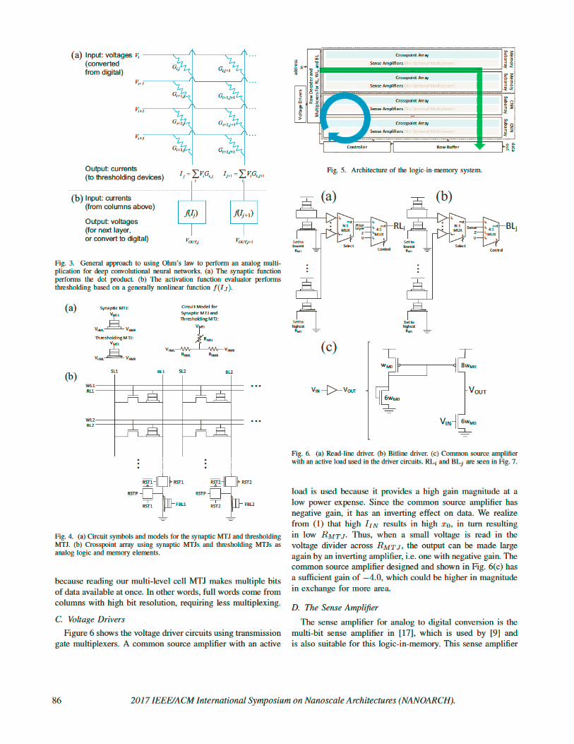
B. System Architecture
The architecture for the logic-in-memory system, includingthe crosspoint array and its associated circuits, is shown inFig. 5. The cell arrays are physically identical but separatedinto memory and CNN subarrays as in [9], but here the CNNdata flow is able to cycle fully in the analog domain.We do not implement column multiplexing in our design,
but suggest it as an option for wider memory subarrays. This is
2017 IEEE/ACM International Symposium on Nanoscale Architectures (NANOARCH). 85
1 , 1j i iji
I VG,j i iji
I VG
Input: voltages(convertedfrom digital)
Output: currents(to thresholding devices)
Gi,j
Gi+1,j
Gi+2,j
Gi+3,j
Gi,j+1
Gi+1,j+1
Gi+2,j+1
Gi+3,j+1
Vi
Vi+1
Vi+2
Vi+3
f(Ij) f(Ij+1)Output: voltages(for next layer,or convert to digital)
Input: currents(from columns above)
…
…
…
…
(a)
(b)
VOUT,j VOUT,j+1
Fig. 3. General approach to using Ohm’s law to perform an analog multi-plication for deep convolutional neural networks. (a) The synaptic functionperforms the dot product. (b) The activation function evaluator performsthresholding based on a generally nonlinear functionf(IJ).
WL1
WL2
...
......
...
SL2 BL2SL1 BL1
RL1
RST1RST1
RST1
RSTP
RST2RST2
RST2
RSTP
FBL1 FBL2
RL2
Synaptic MTJ:
Thresholding MTJ:VMT J
VHML VHM R
VMT J
VHM L VHMRVMT J
VHML VHMR
Circuit Model for Synaptic MTJ and Thresholding MTJ:
(a)
(b)
RMT J
RHMRRHML
Fig. 4. (a) Circuit symbols and models for the synaptic MTJ and thresholdingMTJ. (b) Crosspoint array using synaptic MTJs and thresholding MTJs asanalog logic and memory elements.
because reading our multi-level cell MTJ makes multiple bitsof data available at once. In other words, full words come fromcolumns with high bit resolution, requiring less multiplexing.
C. Voltage Drivers
Figure 6 shows the voltage driver circuits using transmissiongate multiplexers. A common source amplifier with an active
Voltage Drivers
Controller
address
in
Memory
Subarray
Crosspoint Array
Sense Amplifiers (No Optional Multiplexer)
Memory
Subarray
Crosspoint Array
Sense Amplifiers (No Optional Multiplexer)CNN
Subarray
Crosspoint Array
Sense Amplifiers (No Optional Multiplexer)
CNN
Subarray
Crosspoint Array
Sense Amplifiers (No Optional Multiplexer)
...
...
Row Decoder and
Multiplexers for RL, WL, and BL
data
outRow BufferCo
Sen
Multipl
...
Fig. 5. Architecture of the logic-in-memory system.
2:1 MUX
i0
iN-1 s
out
Select
4:1 MUX
i0
i2 s
out4:1 MUX
i0
i3 s
outi1i2
0
RLiZ
0
BLjSense
Con trolCon trol
i1i2Z
PriorLayer
... N:12:1 MUX
i0
iN-1 s
out
Select...
...
N:1
Set to highest RMT J
Set to lowest RMT J
(a) (b)
wM0 8wM0
6wM0
6wM0VIN
VOUT
(c)
VIN VOUT
...
Set to highest RMT J
Set to lowest RMT J
Fig. 6. (a) Read-line driver. (b) Bitline driver. (c) Common source amplifierwith an active load used in the driver circuits. RLiand BLjare seen in Fig. 7.
load is used because it provides a high gain magnitude at alow power expense. Since the common source amplifier hasnegative gain, it has an inverting effect on data. We realizefrom (1) that highIINresults in highx0, in turn resultingin lowRMTJ. Thus, when a small voltage is read in thevoltage divider acrossRMTJ, the output can be made largeagain by an inverting amplifier, i.e. one with negative gain. Thecommon source amplifier designed and shown in Fig. 6(c) hasa sufficient gain of−4.0, which could be higher in magnitudein exchange for more area.
D. The Sense Amplifier
The sense amplifier for analog to digital conversion is themulti-bit sense amplifier in [17], which is used by [9] andis also suitable for this logic-in-memory. This sense amplifier
86 2017 IEEE/ACM International Symposium on Nanoscale Architectures (NANOARCH).

WL1
WL2
... ...
...
...
SL2 BL2SL1 BL1
RL1
RST1RST1
RST1
RSTP
RST2RST2
RST2
RSTP
FBL1 FBL2
RL2
(a)
(b)WL1
WL2
...
...
...
...
SL2SL1
RL1
RST1RST1
RST1
RSTP
RST2RST2
RST2
RSTP
FBL1 FBL2
RL2
BL1 BL2
VIN1
VIN2
IOUT1 IOUT2
IWRITE1 IWRITE2
ISENSE1
VNSENSE1 VNSENSE2
ISENSE2
VWRITE1 VWRITE2
Fig. 7. (a) Feed-forward network operation and (b) memory operations:reading (dashed lines only) and writing (solid lines only) weights.
compares a variable resistor to multiple reference resistors withcontrol logic to encode the resistance level in a multi-bit word.
E. Direct Layer to Layer Connections
Figure 8 shows that a single layer of a deep neural net-work implemented in a CNN subarray can have its outputfeed directly into another layer, meaning that no additionaloverhead is needed for the analog to digital conversion, storagein RAM, and digital to analog conversion as typical in otherCNN implementations. The connection for the analog signalbetween the thresholding function output and the input toanother layer is a long interconnect with an amplifier. Theamplifier in Fig. 8 is the common source amplifier in Fig. 6(c).In the overall system architecture, one CNN subarray outputcould be connected with a long interconnect and amplifier toone or more inputs of another CNN subarray. Connectionsbetween CNN subarrays are programmed with multiplexers.Direct connections between layers speed up deep CNNs.
F. System Operation
Figure 7 illustrates how the logic-in-memory system is op-erated in perceptron mode or in memory mode. In perceptron
... ...
RST1RST1
RST1
RSTP
RST2RST2
RST2
RSTP ...
...
...
SL2 BL2
WL1
WL2
FRL2FRL1
Fig. 8. Any number of layers can be processed in the analog domain, withouthaving to convert each layer result from analog to digital back to analog.
mode, a feed-forward network layer involves these steps:
1) Reset the thresholding MTJs by setting all RSTj=1and inject a DW with RSTP.
2) RSTj=0. WLi= 0. Apply input voltages on RLi. Thecurrents add up on BLj. For each column, the currentinto the thresholding MTJ sets its resistance.
3) BLj= 0. Pass output to the next layer (Fig. 8). If on thefinal cycle, sense the thresholding MTJ resistances.
Only one cycle is required to operate each CNN layer.In memory mode, the steps to read a row of bits are: select
one row with RLi= 0, other RLi= Z, set WLi= 0, and sensethe resistance of each MTJ on BLj.In both modes, the steps to write the synaptic MTJs are:
write one row in the matrix, driving WLi=1; RLi= Z;SLj= 0; repeat for every row, injecting a DW with each BLj.Since all weights in a row are written together, CNNs couldbe trained efficiently in this design.
IV. DISCUSSION
The logic-in-memory system was modeled in a hybridprocess with 45 nm CMOS from the Cadence GPDK and ascaled magnetic tunnel junction process based on [1]. Simu-lations were performed in Cadence Spectre using the processparameters in Table III and results are in Table IV.Power is reported directly from simulations. However,
latency also accounts for the MTJ switching time. In themicromagnetic models, our pulse length t0is 4 ns in Fig. 2,which sets the MTJ switching time. The critical current densityrequirement is met because the MTJ write currents set thebackground current density to over1011A/m2, well abovevalues reported in the literature [18].In our devices, CoFeB is used for the magnetic layers, Ta
forms the heavy metal layer underneath, MgO is used for theinsulating layer, and Ru is used for the contacts. These mate-rials are chosen such that the device exhibits PMA behavior.The MTJ resistance-area product varies exponentially with theMgO thickness. The resistivities we assume are based on ourprevious work in [1] and parameters reported in [4]:
ρCoFeB=2.1×10⁻⁶Ω-m (9)
ρTa=1.9×10⁻⁶Ω-m (10)
ρRu=5.0×10⁻⁷Ω-m (11)
2017 IEEE/ACM International Symposium on Nanoscale Architectures (NANOARCH). 87
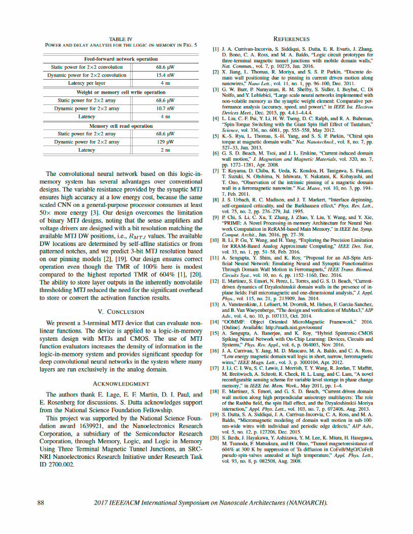
TABLE IVPOWER AND DELAY ANALYSIS FOR THE LOGIC-IN-MEMORY INFIG.5
Feed-forward network operation
Static power for 2×2 convolution 68.6 μW
Dynamic power for 2×2 convolution 15.4 nW
Latency per layer 4ns
Weight or memory cell write operation
Static power for 2×2 array 68.6 μW
Dynamic power for 2×2 array 10.7 nW
Latency 4ns
Memory cell read operation
Static power for 2×2 array 68.6 μW
Dynamic power for 2×2 array 129 μW
Latency 2ns
The convolutional neural network based on this logic-in-memory system has several advantages over conventionaldesigns. The variable resistance provided by the synaptic MTJensures high accuracy at a low energy cost, because the samescaled CNN on a general-purpose processor consumes at least50× more energy [3]. Our design overcomes the limitationof binary MTJ designs, noting that the sense amplifiers andvoltage drivers are designed with a bit resolution matching theavailable MTJ DW positions, i.e.,RMTJ values. The availableDW locations are determined by self-affine statistics or frompatterned notches, and we predict 3-bit MTJ resolution basedon our pinning models [2], [19]. Our design ensures correctoperation even though the TMR of 100% here is modestcompared to the highest reported TMR of 604% [1], [20].The ability to store layer outputs in the inherently nonvolatilethresholding MTJ reduced the need for the significant overheadto store or convert the activation function results.
V. CONCLUSION
We present a 3-terminal MTJ device that can evaluate non-linear functions. The device is applied to a logic-in-memorysystem design with MTJs and CMOS. The use of MTJfunction evaluators increases the density of information in thelogic-in-memory system and provides significant speedup fordeep convolutional neural networks in the system where manylayers are run exclusively in the analog domain.
ACKNOWLEDGMENT
The authors thank E. Lage, E. F. Martin, D. I. Paul, andE. Rosenberg for discussions. S. Dutta acknowledges supportfrom the National Science Foundation Fellowship.This project was supported by the National Science Foun-
dation award 1639921, and the Nanoelectronics ResearchCorporation, a subsidiary of the Semiconductor ResearchCorporation, through Memory, Logic, and Logic in MemoryUsing Three Terminal Magnetic Tunnel Junctions, an SRC-NRI Nanoelectronics Research Initiative under Research TaskID 2700.002.
REFERENCES
[1] J. A. Currivan-Incorvia, S. Siddiqui, S. Dutta, E. R. Evarts, J. Zhang,D. Bono, C. A. Ross, and M. A. Baldo, “Logic circuit prototypes forthree-terminal magnetic tunnel junctions with mobile domain walls,”Nat. Commun., vol. 7, p. 10275, Jan. 2016.
[2] X. Jiang, L. Thomas, R. Moriya, and S. S. P. Parkin, “Discrete do-main wall positioning due to pinning in current driven motion alongnanowires,”Nano Lett., vol. 11, no. 1, pp. 96–100, Dec. 2011.
[3] G. W. Burr, P. Narayanan, R. M. Shelby, S. Sidler, I. Boybat, C. DiNolfo, and Y. Leblebici, “Large-scale neural networks implemented withnon-volatile memory as the synaptic weight element: Comparative per-formance analysis (accuracy, speed, and power),” inIEEE Int. ElectronDevices Meet., Dec. 2015, pp. 4.4.1–4.4.4.
[4] L. Liu, C.-F. Pai, Y. Li, H. W. Tseng, D. C. Ralph, and R. A. Buhrman,“Spin-Torque Switching with the Giant Spin Hall Effect of Tantalum,”Science, vol. 336, no. 6081, pp. 555–558, May 2012.
[5] K.-S. Ryu, L. Thomas, S.-H. Yang, and S. S. P. Parkin, “Chiral spintorque at magnetic domain walls.”Nat. Nanotechnol., vol. 8, no. 7, pp.527–33, Jun. 2013.
[6] G. S. D. Beach, M. Tsoi, and J. L. Erskine, “Current-induced domainwall motion,” J. Magnetism and Magnetic Materials, vol. 320, no. 7,pp. 1272–1281, Apr. 2008.
[7] T. Koyama, D. Chiba, K. Ueda, K. Kondou, H. Tanigawa, S. Fukami,T. Suzuki, N. Ohshima, N. Ishiwata, Y. Nakatani, K. Kobayashi, andT. Ono, “Observation of the intrinsic pinning of a magnetic domainwall in a ferromagnetic nanowire.”Nat. Mater., vol. 10, no. 3, pp. 194–7, Feb. 2011.
[8] J. S. Urbach, R. C. Madison, and J. T. Markert, “Interface depinning,self-organized criticality, and the Barkhausen effect,”Phys. Rev. Lett.,vol. 75, no. 2, pp. 276–279, Jul. 1995.
[9] P. Chi, S. Li, C. Xu, T. Zhang, J. Zhao, Y. Liu, Y. Wang, and Y. Xie,“PRIME: A Novel Processing-in-memory Architecture for Neural Net-work Computation in ReRAM-based Main Memory,” inIEEE Int. Symp.Comput. Archit., Jun. 2016, pp. 27–39.
[10] B. Li, P. Gu, Y. Wang, and H. Yang, “Exploring the Precision Limitationfor RRAM-Based Analog Approximate Computing,”IEEE Des. Test,vol. 33, no. 1, pp. 51–58, Feb. 2016.
[11] A. Sengupta, Y. Shim, and K. Roy, “Proposal for an All-Spin Arti-ficial Neural Network: Emulating Neural and Synaptic FunctionalitiesThrough Domain Wall Motion in Ferromagnets,”IEEE Trans. Biomed.Circuits Syst., vol. 10, no. 6, pp. 1152–1160, Dec. 2016.
[12] E. Martinez, S. Emori, N. Perez, L. Torres, and G. S. D. Beach, “Current-driven dynamics of Dzyaloshinskii domain walls in the presence of in-plane fields: Full micromagnetic and one-dimensional analysis,”J. Appl.Phys., vol. 115, no. 21, p. 213909, Jun. 2014.
[13] A. Vansteenkiste, J. Leliaert, M. Dvornik, M. Helsen, F. Garcia-Sanchez,and B. Van Waeyenberge, “The design and verification of MuMax3,”AIPAdv., vol. 4, no. 10, p. 107133, Oct. 2014.
[14] “OOMMF: Object Oriented MicroMagnetic Framework,” 2016.[Online]. Available: http://math.nist.gov/oommf
[15] A. Sengupta, A. Banerjee, and K. Roy, “Hybrid Spintronic-CMOSSpiking Neural Network with On-Chip Learning: Devices, Circuits andSystems,”Phys. Rev. Appl., vol. 6, p. 064003, Nov. 2016.
[16] J. A. Currivan, Y. Jang, M. D. Mascaro, M. A. Baldo, and C. A. Ross,“Low energy magnetic domain wall logic in short, narrow, ferromagneticwires,”IEEE Magn. Lett., vol. 3, p. 3000104, Apr. 2012.
[17] J. Li, C. I. Wu, S. C. Lewis, J. Morrish, T. Y. Wang, R. Jordan, T. Maffitt,M. Breitwisch, A. Schrott, R. Cheek, H. L. Lung, and C. Lam, “A novelreconfigurable sensing scheme for variable level storage in phase changememory,” in IEEE Int. Mem. Work., May 2011, pp. 1–4.
[18] E. Martinez, S. Emori, and G. S. D. Beach, “Current-driven domainwall motion along high perpendicular anisotropy multilayers: The roleof the Rashba field, the spin Hall effect, and the Dzyaloshinskii-Moriyainteraction,”Appl. Phys. Lett., vol. 103, no. 7, p. 072406, Aug. 2013.
[19] S. Dutta, S. A. Siddiqui, J. A. Currivan-Incorvia, C. A. Ross, and M. A.Baldo, “Micromagnetic modeling of domain wall motion in sub-100-nm-wide wires with individual and periodic edge defects,”AIP Adv.,vol. 5, no. 12, p. 127206, Dec. 2015.
[20] S. Ikeda, J. Hayakawa, Y. Ashizawa, Y. M. Lee, K. Miura, H. Hasegawa,M. Tsunoda, F. Matsukura, and H. Ohno, “Tunnel magnetoresistance of604% at 300 K by suppression of Ta diffusion in CoFeB/MgO/CoFeBpseudo-spin-valves annealed at high temperature,”Appl. Phys. Lett.,vol.93, no. 8, p. 082508, Aug. 2008.
88 2017 IEEE/ACM International Symposium on Nanoscale Architectures (NANOARCH).