a comprehensive hdl model of a line associative …
TRANSCRIPT

University of Kentucky University of Kentucky
UKnowledge UKnowledge
Theses and Dissertations--Electrical and Computer Engineering Electrical and Computer Engineering
2013
A COMPREHENSIVE HDL MODEL OF A LINE ASSOCIATIVE A COMPREHENSIVE HDL MODEL OF A LINE ASSOCIATIVE
REGISTER BASED ARCHITECTURE REGISTER BASED ARCHITECTURE
Matthew A. Sparks University of Kentucky, [email protected]
Right click to open a feedback form in a new tab to let us know how this document benefits you. Right click to open a feedback form in a new tab to let us know how this document benefits you.
Recommended Citation Recommended Citation Sparks, Matthew A., "A COMPREHENSIVE HDL MODEL OF A LINE ASSOCIATIVE REGISTER BASED ARCHITECTURE" (2013). Theses and Dissertations--Electrical and Computer Engineering. 26. https://uknowledge.uky.edu/ece_etds/26
This Master's Thesis is brought to you for free and open access by the Electrical and Computer Engineering at UKnowledge. It has been accepted for inclusion in Theses and Dissertations--Electrical and Computer Engineering by an authorized administrator of UKnowledge. For more information, please contact [email protected].

STUDENT AGREEMENT: STUDENT AGREEMENT:
I represent that my thesis or dissertation and abstract are my original work. Proper attribution
has been given to all outside sources. I understand that I am solely responsible for obtaining
any needed copyright permissions. I have obtained and attached hereto needed written
permission statements(s) from the owner(s) of each third-party copyrighted matter to be
included in my work, allowing electronic distribution (if such use is not permitted by the fair use
doctrine).
I hereby grant to The University of Kentucky and its agents the non-exclusive license to archive
and make accessible my work in whole or in part in all forms of media, now or hereafter known.
I agree that the document mentioned above may be made available immediately for worldwide
access unless a preapproved embargo applies.
I retain all other ownership rights to the copyright of my work. I also retain the right to use in
future works (such as articles or books) all or part of my work. I understand that I am free to
register the copyright to my work.
REVIEW, APPROVAL AND ACCEPTANCE REVIEW, APPROVAL AND ACCEPTANCE
The document mentioned above has been reviewed and accepted by the student’s advisor, on
behalf of the advisory committee, and by the Director of Graduate Studies (DGS), on behalf of
the program; we verify that this is the final, approved version of the student’s dissertation
including all changes required by the advisory committee. The undersigned agree to abide by
the statements above.
Matthew A. Sparks, Student
Dr. Henry Dietz, Major Professor
Dr. Zhi Chen, Director of Graduate Studies

A COMPREHENSIVE HDL MODEL OF A LINE ASSOCIATIVE REGISTERBASED ARCHITECTURE
THESIS
A thesis submitted in partialfulfillment of the requirements forthe degree of Master of Science inElectrical Engineeering in theCollege of Engineering at the
University of Kentucky
ByMatthew Sparks
Lexington, Kentucky
Director: Dr. Henry Dietz, James F. Hardymon Chair in NetworkingProfessor of Electrical & Computer Engineering
Lexington, Kentucky 2013
Copyright c© Matthew Sparks 2013

ABSTRACT OF THESIS
A COMPREHENSIVE HDL MODEL OF A LINE ASSOCIATIVE REGISTERBASED ARCHITECTURE
Modern processor architectures suffer from an ever increasing gap between processorand memory performance. The current memory-register model attempts to hide thisgap by a system of cache memory. Line Associative Registers(LARs) are proposed as anew system to avoid the memory gap by pre-fetching and associative updating of bothinstructions and data. This thesis presents a fully LAR-based architecture, targetinga previously developed instruction set architecture. This architecture features anexecution pipeline supporting SWAR operations, and a memory system supportingthe associative behavior of LARs and lazy writeback to memory.
KEYWORDS: Line Associative Registers, Hardware Description Language, MemoryCaching, Ambiguous Alias, Computer Arithmetic
Author’s signature: Matthew Sparks
Date: April 25, 2013

A COMPREHENSIVE HDL MODEL OF A LINE ASSOCIATIVE REGISTERBASED ARCHITECTURE
ByMatthew Sparks
Director of Thesis: Henry Dietz
Director of Graduate Studies: Zhi Chen
Date: April 25, 2013

Dedicated to my parents, Joseph and Janet Sparks
ACKNOWLEDGMENTS
“If I have seen further it is by standing on the shoulders of giants.”- Issac Newton
I’d like to thank Dr. Randy Fisher, Krishna Melarkode, Nien Lim, and KalyanPonnala for all their work. Without it, this thesis would not have been possible.
I’d also like to thank my advisor, Dr. Hank Dietz, who was an amazing guidethroughout my work on LARs, and who laid much of the foundation on which LARsis based.
Additionally, I’d like to thank my labmate and colleague, Paul Eberhart. He pro-vided the LARK specification that I designed LOON to match, sanity checked manyparts of my design, and provided information on a wealth of other topics.
I want to thank Dr. Raphael Finkel for taking the time to read over my thesis indetail. He provided a great deal of feedback on how to improve the presentation ofmy work.
I would like to thank Dr. Stephen Gedney for encouraging me to pursue my master’sdegree. Without his encouragement, I would not be where I am today.
I also owe a thank you to Dr. Jerzy Jaromczyk, for reminding me that being aman of faith and a man of science are not exclusive.
I would also like to thank my parents, Joseph and Janet Sparks. There is noquestion that I would not have made it through without their care and support.
And on a lighter note, I’d like to thank Anna Tanner, for drawing LOON’s mascotLary the Loon for me.
iii
TABLE OF CONTENTS
Acknowledgments . . . . . . . . . . . . . . . . . . . . . . . . . . . . . . . . . . iii
Table of Contents . . . . . . . . . . . . . . . . . . . . . . . . . . . . . . . . . . iv
List of Tables . . . . . . . . . . . . . . . . . . . . . . . . . . . . . . . . . . . . vi
List of Figures . . . . . . . . . . . . . . . . . . . . . . . . . . . . . . . . . . . vii
Chapter 1 Background . . . . . . . . . . . . . . . . . . . . . . . . . . . . . . . 11.1 Von Neumann . . . . . . . . . . . . . . . . . . . . . . . . . . . . . . . 11.2 Current Problems . . . . . . . . . . . . . . . . . . . . . . . . . . . . . 11.3 Parallel Systems . . . . . . . . . . . . . . . . . . . . . . . . . . . . . . 3
Chapter 2 Line Associative Registers . . . . . . . . . . . . . . . . . . . . . . . 52.1 Solutions to Existing Problems . . . . . . . . . . . . . . . . . . . . . 62.2 Parallelism . . . . . . . . . . . . . . . . . . . . . . . . . . . . . . . . . 7
Chapter 3 History of LARs . . . . . . . . . . . . . . . . . . . . . . . . . . . . 93.1 Precursors to LARs - CRegs and SWAR . . . . . . . . . . . . . . . . 93.2 Line Associative Registers . . . . . . . . . . . . . . . . . . . . . . . . 10
Chapter 4 Implementation of LARs . . . . . . . . . . . . . . . . . . . . . . . . 134.1 Associative Behavior . . . . . . . . . . . . . . . . . . . . . . . . . . . 134.2 One-to-One Data Method . . . . . . . . . . . . . . . . . . . . . . . . 134.3 Single Copy of Data Method . . . . . . . . . . . . . . . . . . . . . . . 144.4 Lazy Copy of Data Method . . . . . . . . . . . . . . . . . . . . . . . 15
Chapter 5 The LOON Architecture . . . . . . . . . . . . . . . . . . . . . . . . 175.1 Instruction Path . . . . . . . . . . . . . . . . . . . . . . . . . . . . . 195.2 Memory System . . . . . . . . . . . . . . . . . . . . . . . . . . . . . . 205.3 Polymorphic Conversion . . . . . . . . . . . . . . . . . . . . . . . . . 255.4 Execution Hardware . . . . . . . . . . . . . . . . . . . . . . . . . . . 285.5 Writeback of Results . . . . . . . . . . . . . . . . . . . . . . . . . . . 41
Chapter 6 Problems with LARs . . . . . . . . . . . . . . . . . . . . . . . . . . 436.1 Input and Output . . . . . . . . . . . . . . . . . . . . . . . . . . . . . 436.2 Self-Modifying Code . . . . . . . . . . . . . . . . . . . . . . . . . . . 44
Chapter 7 Conclusions . . . . . . . . . . . . . . . . . . . . . . . . . . . . . . . 467.1 Results . . . . . . . . . . . . . . . . . . . . . . . . . . . . . . . . . . . 467.2 Future Work . . . . . . . . . . . . . . . . . . . . . . . . . . . . . . . . 46
iv

Appendix A LEPH Table Generation . . . . . . . . . . . . . . . . . . . . . . . 48
Appendix B LEPH Code Generation from Table . . . . . . . . . . . . . . . . . 56
Bibliography . . . . . . . . . . . . . . . . . . . . . . . . . . . . . . . . . . . . 58
Vita . . . . . . . . . . . . . . . . . . . . . . . . . . . . . . . . . . . . . . . . . 61
v

LIST OF TABLES
2.1 Internal Structure of a Line Associative Register (LAR) . . . . . . . . . . 5
5.1 LEPH Conversion, 64-bit slice . . . . . . . . . . . . . . . . . . . . . . . . 275.2 Arithmetic Shift Unit Opcode Table . . . . . . . . . . . . . . . . . . . . 335.3 Arithmetic Shift Unit Opcode Table (continued) . . . . . . . . . . . . . . 345.4 Decomposition of Partial Products, 2 radix multiply highlighted . . . . . 355.5 DPP pyramid form. 2 radix multiply highlighted . . . . . . . . . . . . . 365.6 DPP pyramid form for 8 radix. 4 radix multiply highlighted . . . . . . . 375.7 Division, Shift and Subtract Algorithm . . . . . . . . . . . . . . . . . . . 39
vi

LIST OF FIGURES
3.1 Larry the Loon, mascot of the LOON architecture[24] . . . . . . . . . . . 11
4.1 One-to-One Copy Method Example . . . . . . . . . . . . . . . . . . . . . 144.2 Single Copy Method Example . . . . . . . . . . . . . . . . . . . . . . . . 15
5.1 LOON Pipeline Overview . . . . . . . . . . . . . . . . . . . . . . . . . . 185.2 LOON Memory System . . . . . . . . . . . . . . . . . . . . . . . . . . . 215.3 Memory Bus Guard (MBG) State Machine . . . . . . . . . . . . . . . . . 225.4 Data Load Queue (DLQ) State Machine . . . . . . . . . . . . . . . . . . 235.5 Fetch Queue (FQ) State Machine . . . . . . . . . . . . . . . . . . . . . . 235.6 Instruction Load Queue (ILQ) State Machine . . . . . . . . . . . . . . . 245.7 Memory Writeback Unit (MWU) State Machine . . . . . . . . . . . . . . 255.8 LOON Carry-break Arithmetic Logic Unit . . . . . . . . . . . . . . . . . 305.9 LOON ASU 16-bit Multiplexer . . . . . . . . . . . . . . . . . . . . . . . 325.10 LOON Divider Unit . . . . . . . . . . . . . . . . . . . . . . . . . . . . . 40
vii
Chapter 1 Background
This thesis presents a simple computer architecture using Line Associative Reg-
isters (LARs), targeting an existing demonstration Instruction Set Architecture.[7]
This architecture is implemented in Verilog HDL. It utilizes SIMD Within a Register
(SWAR) to increase parallelism and contains a memory system designed to support
the associative updating and lazy writeback to memory required by LARs.
1.1 Von Neumann
For decades, computing has relied upon the architecture model described by John
von Neumann in his First Draft Report on the EDVAC in 1945, which utilized a pro-
cessing unit with registers and communicated with stored data and instructions in a
separate memory.[17] This model endurs since with few changes, even with challenges
from more recent models such as the Harvard architecture which contains separate
memories for instructions and data. Up until about 1980, memory and processor
performance were comparable, allowing the Von Neumann model to utilize both with
minimal bottle-necking.[11] Ultimately, the varying effects of Moore’s Law on sepa-
rate pieces of computer hardware created problems in the Von Neumann architecture.
Processor performance increased far more rapidly than either memory performance
or bus performance. This discrepancy requires modern processors to include com-
plex cache systems sprawling over 30 to 40 percent of the die which attempt to
hide the massive time penalty incurred when the processor retrieves anything from
memory.[25] This particular delay is known as the “memory gap”.[26]
1.2 Current Problems
Ordinarily, the processor fetches data or instructions from memory and stores them
locally in registers. As processors became relatively faster, waiting on memory to
1

fetch the desired item cost more and more time. To improve performance, processor
designers interposed a memory cache into the bus between the processor and memory.
Caching
Cache consists of a small, fast piece of memory to serve as a buffer between the
processor and the large, slow main memory. The cache hardware makes predictions
about which data is likely to be requested by the processor based on the location and
time the processor requested previous data. For example, the processor is likely to
request several sequential memory locations if walking through an array. Therefore,
the cache will hold memory locations nearby to a processor request to take advantage
of this spatial locality. The other metric commonly implemented by a cache takes
advantage of repeated requests to a memory location by the processor. Since the
processor is likely to revisit the same memory locations, those locations will be held in
cache to take advantage of temporal locality. Common processor architectures today
incorporate three or more levels of cache to minimize any potential delay between
processor and memory as much as possible.
Branch Prediction
When applied to instructions, this cache system leads to a problem in predicting
branches in a program. In the original model proposed by von Neumann, standard
orders were fetched singly from memory. Once fetched and decoded, they were exe-
cuted and the processor fetched the next standard order. Obviously, this arrangement
would result in a request to memory upon every instruction, which is undesirable due
to the effects of the memory gap. Caches can utilize spatial locality and hold the
sequence of instructions likely to be next requested, but upon a branch occurring,
spatial locality no longer applies. Branch prediction combats this consequence by at-
tempting to predict whether a branch is taken or not, and holding the corresponding
instructions. In modern pipelined architectures, where several instructions can be
in varying stages of execution, missing a branch prediction has the additional effect
of requiring all instructions already being executed to be flushed from the pipeline.
2

Therefore most modern processors employ hefty branch prediction hardware, which
may contain “taken”/“not taken” histories for several branches simultaneously.
Ambiguous Aliasing
One additional concern arises from the use of memory-cache systems, known as
the “ambiguous alias” problem.[1, 3] This problem arises when pointers to arrays are
not known at compile time and may point to the same value. If two pointers are
referenced to load array data into registers, the array data for both could be loaded
into registers from the same location in memory. If so, operations on one of the
pointers must be mirrored to the other copy of the array data. As the values of the
pointers are uncertain, after every change this array data must be flushed back into
memory and reloaded into the registers again. Considering the increasing penalty of
the memory gap, eliminating this problem is highly desirable. One approach proposed
by researchers is to incorporate memory-cache behavior into the registers themselves
by associatively updating objects inside the registers. [5]
1.3 Parallel Systems
Aside from cache systems, designers adapted the von Neumann model to be highly
parallel. Methods for increasing processor performance may be broken into two cate-
gories: the speed at which the processor executes operations may be increased or the
number of operations executed simultaneously may be increased.
Very Long Instruction Words
Very Long Instruction Word (VLIW) is an architectural method that takes advan-
tage of the latter approach.[4] Instead of executing a single operation per instruction,
VLIW packs several instructions, usually seven to thirty, into a single packet to be
fetched and executed simultaneously. In order to execute in this fashion, the in-
structions must have no interdependencies; simultaneous execution precludes using
the result of one instruction as an operand of another simultaneous instruction. In
3
a VLIW architecture, ensuring no interdependencies is accomplished prior to execu-
tion by the complier, a program responsible for converting source code to executable
machine code. This trait distinguishes VLIW from the superscalar architecture com-
monly found in modern processors, which incorporate scheduling hardware to deter-
mine which instructions can be executed at the same time. Maintaining the flow
of these very large instructions into the execution pipeline aggravates the memory
gap problem. One approach suggested by researchers to alleviate this problem is to
compress the instructions before loading them from memory and decompress them
inside the processor. This compression keeps the amount of memory bandwidth used
to a minimum.[15]
SIMD Within A Register
Another method of performing multiple operations simultaneously is via a Single
Instruction Multiple Data (SIMD) type architecture. While SIMD was originally
implemented as entire dedicated machines such as the MasPar MP-1, it is more
commonly found in today’s processors as SIMD Within A Register, commercialized
as AVX and SSE.[2] While VLIW relies on parallelism at the instruction level, SWAR
instead takes advantage of a single instruction executed on several pieces of data in
parallel. While most modern processors take advantage of executing single operations
on several fixed width pieces of data, SWAR as a general model may be applied to data
fields of varying width.[9] SWAR suffers from the memory gap similarly to VLIW,
although the requirements of the instruction fetch are eased, as only one instruction
is valid for many pieces of data.
Copyright c© Matthew Sparks, 2013.
4

Chapter 2 Line Associative Registers
The solution proposed by researchers Krishna Melarkode and Henry Dietz to these
standing problems in computer architecture is Line Associative Registers. LARs is
a new memory model derived by Krishna Melarkode and Henry Dietz at the Uni-
versity of Kentucky from CRegs.[14] LARs contain an entire line of data between
256 and 4096 bits instead of the single unit of data held by conventional registers,
and supplement this line of data with meta data tags. These meta data tags hold
information regarding the size and type of data contained in the LAR, along with the
memory address at which the data is located. LARs thus blend the characteristics
of registers and conventional memory caches. Additionally, LARs are associatively
aliased: if two LARs reference the same memory address, both will update if one or
the other is changed. The structure of a LAR is shown in Table 2. In this work, we
implement LARs holding 2048 bits of data. This keeps bus widths inside the design
to a reasonable width while taking advantage of the parallelism inherent in LARs.
Table 2.1: Internal Structure of a Line Associative Register (LAR)
Physical Memory Address Type Size Data64 bits 2 bits 2 bits 2048 bits
[63:8] Physical Memory Base Address [7:0] Offset within LAR 00 - Reserved 00 - 8-bit objects01 - Unsigned Int 01 - 16-bit objects10 - Signed Int 10 - 32-bit objects11 - Float 11 - 64-bit objects
The compiler loads a LAR staticly, instead of requiring hardware to dynamically
load cache. For example, a LAR for holding instructions, known as an ILAR, must
be loaded directly from memory using a FETCH instruction instead of conventional
hardware predicting which branch is likely to next run. Similarly, a LAR for data,
known as a DLAR, must be loaded from memory via a LOAD instruction. Once a line
of data or instructions is loaded into a LAR, individual pieces of data or instructions
may be addressed by offset with the LAR.
5
2.1 Solutions to Existing Problems
This combination of long data lines, associative behavior, and static prediction
presents a unique solution to the memory-gap problem. Ordinarily, cache hardware
predicts which data are likely to be next accessed, and will sometimes miss, leading
to increasingly expensive accesses to memory at unpredictable points in program
execution. A LAR-based architecture instead relies on the compiler scheduling these
accesses at points in the program where the least delay will be incurred. For example,
in a conventional modern architecture, if a program jumps to accessing a second set
of data at a different point in memory, the initial access to that address will likely not
be predicted, and the program will have to wait while the requested data loads from
memory. While modern compilers attempt to shuffle instructions to minimize such
delays, such optimizations rely on assumptions about how the architecture makes
cache predictions. In a LAR-based architecture, loading the second set is an explicit
instruction in the hardware, and can be scheduled by the compiler well before that
data is required by the processor.
Branch Prediction
Similar benefits apply to branch prediction. If branch prediction hardware misses,
a modern pipelined architecture not only must wait for the new branch of instruc-
tions to LOAD, but must flush the pipeline of incorrect instructions. In a LAR-based
architecture, branch instructions do not reference memory directly, but instead point
to locations in ILARs. The compiler fetches both branches of instructions, and pro-
gram execution is simply directed into one ILAR or another based on the result of
the branch instruction.
Ambiguous Aliasing
The associative behavior of LARs address the “ambiguous alias” problem. This
problem arises by loading addresses from memory which are not known at compile
time. In a conventional architecture, this uncertainty might result in resolving the
6

same memory address into multiple registers, potentially causing loss of changes to
one register or the other. However, LARs contain an address tag. If two mem-
ory references resolve to the same memory address, the corresponding LARs will be
associated and updated simultaneously.
2.2 Parallelism
There are two primary methods of increasing performance in computing. The first
method is simply to increase the speed at which tasks are executed. The second
is parallelism, which in computing refers to running several tasks simultaneously as
a method of increasing performance. Within the past decade, transistors within a
processor chip became dense enough that increasing clock speed created more heat
than could be dissipated, resulting in chip failure. Parallelism is increasingly common
in modern architectures to avoid the so-called “thermal wall”.
SIMD Within A Register
Since a data LAR holds an entire line of data consisting of many individual words,
a LAR-based architecture can support vector operations on entire LARs. This char-
acteristic allows a LAR-based architecture to perform vector operations similar to
those specified by SSE and AVX in modern architectures. Since LARs contain type
and size tags, a LAR-based architecture can also perform these vector operations
on multiple word sizes although this resizing requires significant support within the
execution pipeline.
Multiple Instruction Fetch
An additional facet of parallelism in a LAR-based architecture is found in the in-
struction pipeline. Since an entire line of instructions can be held in a single ILAR,
a LAR-based architecture displays many of the characteristics of a Very Long In-
struction Word (or VLIW) system. Both architectures fetch an entire sequence of
instructions from memory with each access. To avoid starving the pipeline, a LAR-
7
based architecture should also perform some kind of instruction compression as is im-
plemented in many VLIW architectures.[15] This method would need to decompress
relatively quickly and decompress to the fixed size of an ILAR. Finding a suitable
method remains an open topic of research and is not addressed in this work.[13]
Copyright c© Matthew Sparks, 2013.
8

Chapter 3 History of LARs
Line Associative Registers are a combination of several separate pieces of work, heav-
ily associated with Dr. Henry Dietz during his tenure at Purdue University and the
University of Kentucky. The associative and cache replacement characteristics of
LARs originated from the idea of Cache Registers, while SIMD Within A Register
provided the vector arithmetic integral to LARs.
3.1 Precursors to LARs - CRegs and SWAR
LARs evolved out of Cache Registers (CRegs) originally proposed by Henry Dietz
and Chi-Hung Chi in 1988.[6] CRegs were proposed as a solution to ambiguously
aliased values, and consisted of a conventional single-datum register tagged with a
memory address. CRegs update associatively based on the memory address, just
as LARs do. However, they still only hold a single word, thus lacking the vector
arithmetic and instruction prefetch provided by LARs.[5]
SIMD Within A Register
In computing, a SIMD architecture allows for a single instruction to operate on
many words at once. Such architectures were originated in the 1970s and became
common in the 1980s, allowing a single instruction to be distributed to many cores
operating on different data. However, computers based on this architecture could
be difficult to program efficiently due to the difficulty of keeping as many processors
as possible doing useful work when limited to one instruction at a time. Randall
Fisher explored the concept of allowing this behavior in a single register in 2003 in
his dissertation as a way to allow some of the benefits of SIMD in a more traditional
architecture.[9] Instruction extensions such as SSE and AVX later commercialized
SIMD Within a Register, which is now commonplace in modern processors.
9

3.2 Line Associative Registers
Following the concepts of SWAR and CRegs, Krishna Melarkode first proposed
Line Associative Registers in 2004, with the explicit purpose of combining the ideas of
“Vector Registers”, “tagged memory architectures”, and “aliasing, register allocation,
and solutions in hardware”.[14] This work explored both instruction LARs and data
LARs and provided a simple simulator written in C. Melarkode focused on the effects
of LARs on accessing memory and proposed an instruction set architecture with load,
store, and fetch instructions for moving the contents of DLARs and ILARs into and
out of memory.
Instruction LARs
In 2009, Nien Lim implemented the first HDL version of ILARs in his master’s
thesis at the University of Kentucky. His work provided some insight into the work-
ings of the FETCH instruction which is required in any LAR-based architecture to
fetch instruction blocks from memory into ILARs. He also examined the SELECT
instruction, the LAR-based equivalent to a branch instruction. Lim also investigated
various compression algorithms for fetching instructions and concluded that com-
pression methods suitable for ILARs need to be lossless, and need to decompress in
constant or near constant time.[13]
Data LARs
Lim’s work tied in closely with an HDL implementation of DLARs by Kalyan Pon-
nala in 2010, also as a master’s thesis.[20] His work explored the SWAR characteristics
of DLARs, including executing both scalar and vector operations upon a LAR, and
the associated type conversions necessary due to the type tagging present in DLARs.
Ponnala also explored some of the data and structural hazards caused by using a
DLAR bank versus a traditional register file.
10

Figure 3.1: Larry the Loon, mascot of the LOON architecture[24]
LARK Compiler
Ultimately, LARs require significant support from the assembler and compiler to
function, since conventional tools do not handle manual instruction fetches and data
loads. At the University of Kentucky, Paul Eberhart proposes designing a toolchain
based on the LLVM compiler architecture specifically for LARs.[7] This compiler
targets a viable instruction set architecture known as LARs at Kentucky (LARK)
which supports all necessary memory and branching operations for LARs, as well as
both scalar and vectorized arithmetic operations.
Comprehensive Model
To date, no comprehensive model incorportating LARs throughout the design ex-
ists. Lim’s work utilized conventional registers in the datapath, while Ponnala im-
plemented a relatively standard instruction fetch procedure. This work presents a
comprehensive, fully LAR-based, six-stage pipelined logical design implementing the
LARK ISA supporting LARs in both the instruction and data paths. My implemen-
tation of this processor architecture, known as LOON, is written in the Verilog-2001
hardware design language. It provides examples of fetching and accessing instructions
in an ILAR-based bank along with branching within that bank. It utilizes a two-part
DLAR bank, storing tag information and stored data respectively, and demonstrates
11

loading from memory, “lazy” writebacks to memory, and storage of both vector and
scalar results. Finally, the execution pipeline shows the polymorphic conversion hard-
ware necessary to execute on LARs of different data types and sizes and the vectorized
execution units necessary to operate on LARs, including multiplication and division.
Copyright c© Matthew Sparks, 2013.
12

Chapter 4 Implementation of LARs
The concept of LARs can be implemented in a variety of ways, particularly their
associative behavior. They can be implemented as individual registers, which means
each LAR has a one-to-one relationship with the data stored in that LAR. They
can be implemented as a separate namespace, where aliased LARs point to only one
physical copy of the data. These two techniques can also be hybridized, where each
LAR keeps an individual copy, but some copies exist only for redundancy if the main
copy changes address.
4.1 Associative Behavior
The LARK ISA elaborates on several aspects of the associative behavior of LARs.
Association of LARs is based on the high-order bits of the memory address. The
address field may contain an offset within a LAR, which is referenced for pointer
behavior handled by the compiler. This address field also provides the offset of LAR
data used in address calculations. However, this offset is represented in the low-order
bits, which are ignored by the associative update mechanism. The high-order bits
indicate the memory block contained within a LAR. The LOON memory system
forces alignment to avoid separate LARs containing overlapping blocks.
The memory address is the only LAR information that affects associativity. As-
sociated LARs may differ in size or type tags, which affects how the LOON pipeline
executes operations on the contained data.
4.2 One-to-One Data Method
First, there can be as many copies of the data as there are aliases. Under this
method, upon assignment of a new alias, a copy of the data is made from an existing
alias. Any operation writing to any aliased register must immediately update other
13
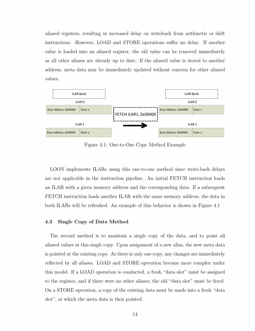
aliased registers, resulting in increased delay on writeback from arithmetic or shift
instructions. However, LOAD and STORE operations suffer no delay. If another
value is loaded into an aliased register, the old value can be removed immediately
as all other aliases are already up to date. If the aliased value is stored to another
address, meta data may be immediately updated without concern for other aliased
values.
���������������
������
��������������
������
������
������
�������
���������������
������
���������������
������
������
������
�������
����������� � �
Figure 4.1: One-to-One Copy Method Example
LOON implements ILARs using this one-to-one method since write-back delays
are not applicable in the instruction pipeline. An initial FETCH instruction loads
an ILAR with a given memory address and the corresponding data. If a subsequent
FETCH instruction loads another ILAR with the same memory address, the data in
both ILARs will be refreshed. An example of this behavior is shown in Figure 4.1
4.3 Single Copy of Data Method
The second method is to maintain a single copy of the data, and to point all
aliased values at this single copy. Upon assignment of a new alias, the new meta data
is pointed at the existing copy. As there is only one copy, any changes are immediately
reflected by all aliases. LOAD and STORE operation become more complex under
this model. If a LOAD operation is conducted, a fresh “data slot” must be assigned
to the register, and if there were no other aliases, the old “data slot” must be freed.
On a STORE operation, a copy of the existing data must be made into a fresh “data
slot”, at which the meta data is then pointed.
14

Figure 4.2: Single Copy Method Example
The LOON architecture implements DLARs in this manner. Reference counts are
kept for each line of data, and lines are considered free when their reference count
is zero. LOAD and STORE are the only instructions that affect these reference
counters. Both a LOAD and a STORE instruction will increment the reference count
of the newly assigned line of data, while decrementing the reference count of the
previously used line of data. An example showing aliased LARs is shown in Figure
4.2.
4.4 Lazy Copy of Data Method
A hybridization of the two previously described methods may also be implemented.
This method conducts “lazy copies”. There are as many copies of the data as there
are aliases; however, the strict requirement to have all copies up to date at all times is
lifted. Instead, a “current” bit is added to track the current state of the copy relative
to the original, and a lazy copy mechanism updates aliased copies in its own time.
When a new alias is created, a slot for its copy of the data is made and flagged as not
“current”. If an operation writes to aliased data, only the master copy is updated
immediately and all other copies are merely flagged as not “current”. LOAD and
15
STORE operations remain complex under this schema. A LOAD operation on any
aliased copy other than the original may execute immediately. However, if the register
containing the original data is loaded, the hardware must ensure that at least one
aliased copy is “current” and flag that copy as the new original. Similar guards must
be implemented for a STORE operation; if the original is stored to a new address, a
new original must be selected. Additionally, if an aliased copy is stored, it must be
“current” before the meta data is changed to a new address.
Copyright c© Matthew Sparks, 2013.
16

Chapter 5 The LOON Architecture
The LOON architecture pipeline takes a similar structure to that of other proof-of-
concept architectures such as the original MIPS design.[10] This pipeline contains a
total of six stages: Instruction Fetch/Decode (ID/IF), Meta Data Fetch (MDF), Line
Data Fetch (LDF), Shift and Convert Data (SH/CD), Execute (EX), and Writeback
(WB). The memory system is decoupled from the pipeline, and runs independently.
The pipeline is not interlocked but can be stalled by some conditions, such as refer-
encing an ILAR or DLAR that is not fully loaded yet. Control signals are stacked
into the pipeline in the Instruction Fetch/Decode stage, and are passed through the
pipeline similarly to data. An overview of the LOON pipeline may be found in Figure
5.1.
17

ID/IF
PIpelIne
RegIster
MDF
PIpelIne
RegIster
LDF
PIpelIne
RegIster
CD/SH
PIpelIne
RegIster
EX
PIpelIne
RegIster
� � � �
� � � � �
� � � � � � � �
� � � � � � � � �
� � � � � �
� � � �
� � � � �
� � � � � � � �
� � � � � � � � �
� � � � � �
� � � � � � � � � �
� � � � � � � � � �
�� !"
#$%&
' � � � � � � �
' � � � ( � � )
' � � � * � � �
' � � � ( � � )
+ , - . / 0
1 2 3 4
5 6 7 8 9
:�;"# <$==#�>>$==�#
?# @A B:CD
E � � � ( � � )
F G H . 7 8 I J K L M N O
P � � � � Q � � )
� � � � � R * � S )
� � � �
� � � �
' � � � � � � T
� � � � � � ' � �
UVWXUVWY
M Z L J 0
J Z + [ \ 8 7 / 3
+ Z K 7 6 3 ] ^ /
_�>C`!a�`� !
�� !"
#:C`!bc
`b�#
�� !"#
dbeb =�
#
�� !"
#aBbf!&Ab!
gh
gh
gh
gh
i � * � � � �
� � S � �
i � * � � � �
� � S � �
i � * � � � �
� � S � �
Figure 5.1: LOON Pipeline Overview
18

5.1 Instruction Path
The instruction path in LOON is relatively conventional. Instructions are fetched
from memory and stored into ILARs. Once in the ILAR bank, the Program Counter
(PC) selects an instruction to be decoded and sent down the pipeline.
ILAR Bank
The ILAR bank itself is where LOON most differs from other architectures. The
ILAR bank consists of 256 LARs, which only contain a memory address field and a
data field. Since instructions are implicitly 64 bits long under the LARK ISA, the
type and size fields usually found within a LAR are omitted. Instructions are fetched
from memory in a block of 32 instructions, which fills one ILAR. A single FETCH
instruction can specify for up to sixteen of these blocks to be loaded from memory,
which is executed in by the memory subsystems and takes place decoupled from the
pipeline. As instructions are loaded into the ILAR bank, any memory addresses
loading are checked against addresses already in ILARs. Any aliased addresses will
also latch the fetched instructions, thus ensuring that aliased ILARs remain identical.
Since this operation is the only action which can change an ILAR, the two-part
structure used by the DLAR bank is unnecessary.
Instruction Selection And Decoding
Instruction decoding begins with selecting an instruction from the ILAR bank
using the Program Counter, or PC. Notably, the Program Counter in the LOON
architecture has no relation to memory addresses, as in other architectures such as
MIPS.[10] Instead, the first portion of the PC references an ILAR, while the second
portion references an offset within that ILAR. In LOON, the first five low-order bits
[4:0] of the PC reference ILAR offset, while the next eight bits [12:5] reference an
ILAR within the ILAR bank.
19
Once the instruction is selected, the LARK Decoding Unit (LDU) decodes it. The
LDU generates all necessary control signals for the LOON architecture and passes
them into the pipeline registers to be directed to the appropriate modules.
5.2 Memory System
The LARK memory system centers around the key concept of “lazy” writeback
to memory. The LARs themselves hold data the majority of the time, and writing
data back to memory is automatically handled by the hardware. An overview of the
memory system may be found in Figure 5.2.
Memory Bus Guard (MBG)
The memory bus guard (MBG) acts as arbitrator between data reads, data writes,
and instruction reads accessing a single random-access memory or RAM that contains
both instructions and data. In a LAR-based architecture, since writeback to memory
is “lazy”, data writes are lowest priority while data reads are considered highest
priority. Instruction reads are prioritized higher than data writes but lower than
data reads. Memory is accessed via a single address bus for both reads and writes
and two 2048-bit wide buses for reading and writing cache-length lines respectively.
The MBG communicates with the data load queue, the instruction load queue, and
the memory writeback unit, and does not perform queuing of reads or writes on its
own. A logic diagram of the state machine within the MBG may be found in Figure
5.3.
Data Load Queue(DLQ)
The data load queue (DLQ) communicates between the DLAR Line Data Bank, the
memory bus guard, and the LOON Controller. LOAD instructions send a request
to the DLQ, which then puts in a request to the MBG. Once the MBG services
the request of the DLQ, it takes the provided data and attempts to write it to the
appropriate DLAR in the Line Data Bank. The Data Load Queue contends for the
20

jkl
mnmopqqr
lstuvw xyz
{y|v}
~lx{�
lstuvw
�v��s�|�� ����
~l���
�|�| �u|}
�ysys
~����
��z�vy���u�
�u|}
�ysys
~����
�s��� �ysys
~���
mnmoqp�por
mnmoqp�po�
�r��nrnpq
rrq��rq�
�r��nopqqr
�r��noqp�p
�r��norq�
�r��noq��n
�����������
�����������
����������
�����������
�����������
�����������
����������
�����������
���s �|�| x|��
~��x�
���no��r
���noqp�p
�n�q��
�r��n
����
¡��¢���
����
ls�| �|�| x|��
~l�x�
�n�q��
�o��r
���no��r
���noqp�p
���nopqqr
�r��n
mn�popqqr
���no��ro��
���nopqqr
���no��ro�£�
���noqp�p
��kj x|��
¤�¥�¦¦��
¤�����¢���
¤���������
¤�����§��
¤�������¡�
¤�¥�¦¦��
¥�¦¡���§©¢�
¥�¦¡�¢���
�n�q�� o��r
ª«�����
��§��¡��
ª«��§§���
¬r�m® �p n
Figure 5.2: LOON Memory System
21

��������
������ �
��������
�������������������
����
��������
�������������������
����
��������
��������������������
����
��������
����� ��������������
������������
��������
����� ��������������
������������
��������
����� ���������
������������������
°±²³´ µ¶·¸¶¹º
»¼½ ¾µ¿Àµ¿ºÁ
µ¿º¶ µ¶·¸¶¹º
ÃÄÅ ¾µ¿Àµ¿ºÁ
ÆÇÈÉ µ¶·¸¶¹º
ÊËÌʾµ¿Àµ¿ºÁ
ÍÈÎÏÀº µ¶ÐÑÁ
ÍÈÎÏÀº µ¶ÐÑÁ
ÍÈÎÏÀº µ¶ÐÑÁ
ÒÓÔÕÖ×Ö
ÖØÖÙÚÖÛÚÜ
ÍÈÎÑкÐ
ÐÝпÞÐßÞ¶
ÍÈÎàÀÏ῵â¹
㵿º¶ àÀâ¾Þ¶º¶
ÉÆäåйÏÀº àÀÏ῵â¶Ñ
æÆäåйÏÀº àÀÏ῵â¶Ñ
ÎÂçåйÏÀº àÀÏ῵â¶Ñ
• èéêë êëëì íé îïð ñòó
• ôõö÷êø ùéì îïð ìúêë
• èéêë êëëì íé îïð ñòó
• ôõö÷êø ùéì îïð ìúêë
• èéêë êëëì íé îïð
ñòó
• ôõö÷êø ùéì îïð ûìõíú
• üòí îïð ìúêë ëêíê é÷
ýèþ ëêíê ñòó
• ôõö÷êø ýèþ íÿêí ìúêë õó
ìúêë�
• üòí îïð ìúêë ëêíê é÷
�èþ ëêíê ñòó
• ôõö÷êø �èþ íÿêí ìúêë õó
ìúêë�
• ôõö÷êø ð�� íÿêí ûìõíú
õó ëé÷ú
• �øúêì êøø ñòóúó ê÷ë
ìúêë� óõö÷êøó
Figure 5.3: Memory Bus Guard (MBG) State Machine
write port on the DLAR Line Data Bank with the Writeback (WB) stage of the
processor. Since the WB stage is time sensitive, it is possible for the Data Load
Queue to be pre-empted. If this pre-emption occurs, the Data Load Queue attempts
to write again on following clock cycles until the write completes. For demonstration
purposes, the Data Load Queue only handles one LOAD instruction at a time. In a
more advanced architecture, the DLQ could be expanded to handle multiple LOAD
requests to the Memory Bus Guard. A logic diagram of the state machine within the
DLQ may be found in Figure 5.4.
22

��������
����� �����
������� �
��������
������ ������
��������
������ ��������� ��
���
�� ����� ���
�� �������
����� ����
��� ���� ��� ���� ����
�� ���� ����
• ��� ���� ! "#$ %�&• '(� �(�� �(��) * � "#$• ��� +�� ! ,-./ %�!0 %�&• � 1!� +(!�1!2 �� +�� !,-./ %�!0 %�&
• '(� +(!�1!2• '(� %�&)
�� ��3�4 ��56�
�� �3�4 ��56� ��
• 7 � %�&)
• 89(�� �(�� �(��) * � "#$• ��� "#$ ���� ! ,-./ %�!0%�&
• 8 ::1� ;�1�( � ,-./ %�!0
• 89(�� ;�1�( � ,-./ %�!0
• 89(�� %�&)
Figure 5.4: Data Load Queue (DLQ) State Machine
��������
������� ���
�������������
��������
������������
��������
�������� ��!��"�#
<= >?@AB CC A@DEB?BFG
• HIJ KLMN• HIJ OLPQJRJST JR JRJSTOLPKIU RV WXYZM JR VIJ[\
• HIJ WX] ^JU JR ^UR_`aIa bcHd• HIJ WX] SaaU JR ^UR_`aIa SaaU• HIJ ^IOa`Oe JU JR bcHd• HIJ PSUf ^IOa`Oe• HIJ [RLOJ JR gIUR
<= A?hijkl mno@npB
<= hijkl mno@npBnq
• rst uvwx
• yz{|} ~|}� �{�����• �wwv{ ���� ts ���
�������$
��������%��� ���
�����������%�
<= A@DEB?BFG � �
• yz{|} ���� ts ���• ���}{~{�t ���� �s��t{}• ���}{~{�t ~{~s}x|��}{ww ux ���
• yz{|} uvwx
<= >?@AB � A@DEB?BFG
• ���}{~{�t �sv�t• ���}{~{�t �{����� �t}
<= <�� A?B q?An
<= <�� q?An
• �{�}{~{�t �v~�tst|z• �wwv{ ���� ts ���
<= A@DEB?BFG CC �
Figure 5.5: Fetch Queue (FQ) State Machine
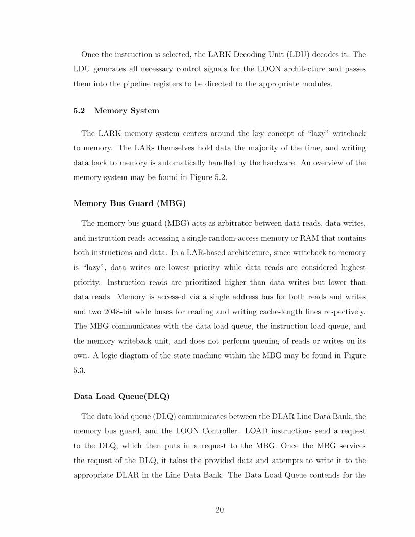
Fetch Queue (FQ) and Instruction Load Queue (ILQ)
The process for fetching ILARs is slightly more complex. While a LOAD instruction
specifies a single DLAR, a FETCH instruction may specify up to sixteen ILARs to be
fetched from memory. There are two modules responsible for FETCH instructions.
23
The first, the Fetch Queue (FQ), receives FETCH instructions, and communicates
with the ILAR bank and the Instruction Load Queue. It marks all affected ILARs
as pending to prevent decoding of instructions from an out of date ILAR. The Fetch
Queue then generates the specified addresses from the FETCH instruction, and sends
the requests sequentially to the Instruction Load Queue. The Instruction Load Queue
(ILQ) is the ILAR counterpart to the Data Load Queue. The ILQ behaves in a similar
manner, and communicates between the ILAR bank and the Memory Bus Guard
as the DLQ does, but communicates with the Fetch Queue instead of the FETCH
instruction directly. Logic diagrams of the state machines within the FQ and ILQ
may be found in Figure 5.5 and Figure 5.6 respectively.
��������
����� ���
��������
������ �����
��������
������ � ����� �
���
�� ������� ����
�� ���������� � ¡¢£��¤¡ ¤�¥
• ¦§¨ ©ªª« ¬ ®¯° ±§²• ³´¨ «´©ª «´©ªµ ¶¬« ®¯°• ¦§¨ ·¨« ¬ ¸¹º» ±©¼ ±§²• ¦¬½¨ ·´ª½¾ ©¨ ·¨« ¬¸¹º» ±©¼ ±§²
• ³´¨ ·´ª½¾• ³´¨ ±§²µ
�� ��¿ÀÁ ��ÃÄ�¡�
�� ¿ÀÁ ��ÃÄ�¡���
• Ŭ¨ ±§²µ
• ÆÇ´©« «´©ª «´©ªµ ¶¬« ®¯°• ¦§¨ ®¯° ª©¨© ¬ ¸¹º» ±©¼±§²
• ƬÈȽ¨ É«½¨´ ¨¬ ¸¹º» ±©¼
��������
����������� �!"�"�
�� � ��� Ê��¡¢£��¤��
• ÆÇ´©« É«½¨´• ³´¨ ª¬´ ²½¾©Ç ¨¬ ËÌ
• ÆÇ´©« ª¬´
Figure 5.6: Instruction Load Queue (ILQ) State Machine
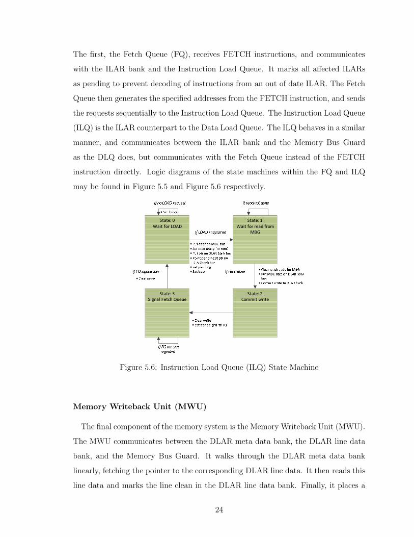
Memory Writeback Unit (MWU)
The final component of the memory system is the Memory Writeback Unit (MWU).
The MWU communicates between the DLAR meta data bank, the DLAR line data
bank, and the Memory Bus Guard. It walks through the DLAR meta data bank
linearly, fetching the pointer to the corresponding DLAR line data. It then reads this
line data and marks the line clean in the DLAR line data bank. Finally, it places a
24

write request to the Memory Bus Guard using the retrieved meta data and line data
and waits until the MBG confirms that the data is written to memory. The Memory
Writeback Unit then moves on to the next DLAR and repeats the process. A logic
diagram of the state machine within the MWU may be found in Figure 5.7.
��������
����� �����
��������
��������������
��������
��������������
��������
������������������
ÍÎ ÏÐÑÒÓÐÒÓÔÕ
ÖÒÓÔ×Ø ÙÐ ÔÐ Ú
ÍÎ ÑÒÓÐÒÓÔÕ
ÖÒÓÔ×Ø ÙÐÔÐ Û
• ÜÝÞßà áâã äå ßæçèåÞé
• êèßéÞëÞèå ßæçèåÞé
• ìÞå íîèÞ ïäåä äå
ðéîæéîåñ ðæîèåÞé• òçå áâã ëÞëæéñ
äïïéÞóó æè ôéîåÞ õçó
• ìÞå íîèÞ ïäåä äå áâã
ðæîèåÞé
• òçå ïäåä æè ôéîåÞ õçó
• öíä÷ äó éÞäïñ åæ øùì
ÍÎ úûÔû Óü
ýþ×ûÏ
ÍÎ úûÔû Óü
ÏÐÔ ýþ×ûÏ
ÍÎÿ�� ÏÐÔ
úÐÏ×
ÍÎÿ��
úÐÏ×
• ãÞëæ Þ
éÞäïñ !íä÷
Figure 5.7: Memory Writeback Unit (MWU) State Machine
5.3 Polymorphic Conversion
A key part of implementing LARs in a pipeline is the capability to operate on
several word sizes “on the fly” in sequential instructions, and possibly within a single
operation. Issuing an instruction to add an 8-bit value to a 16-bit word and store the
result as a 32-bit representation is entirely valid within the LARK instruction set.
The pipeline must therefore contain polymorphic hardware to transform data from
its stored type to the type desired for the operation.
25

Shift Conversion Unit
The first step in SH/CD stage is to shift the target DLAR data into position. If the
instruction executing is a vector operation, this step is unnecessary as operation will
affect the entire DLAR. If the operation is scalar, the Shift Conversion Units align
data at the specified offsets to the zero offset position. The data is then ready to be
converted into the appropriate data type.
As this particular implementation is limited to signed and unsigned integer types
and does not implement floating-point arithmetic, the requirements of this polymor-
phic hardware are simplified. To further ease implementation, saturation logic will
be outside the scope of this project. When converting a number from a higher-bit to
a lower-bit type, the number may be outside the range of its new type. For example,
-32768 cannot be represented as an 8-bit value. If saturation logic were implemented,
the result of converting such a number would be the closest result in the new rep-
resentation: -32768 would be changed to -127. However, this conversion requires a
significant amount of logic to implement. Therefore, LOON implements such out-of-
range conversions as simple truncations. The LOON Example Polymorphic Hardware
(LEPH) performs conversions between all signed and unsigned datatypes by selecting
or sign-extending selected 8-bit words from the input since LARK does not implement
data types smaller than 8 bits.
Selection Process
These selections are implemented by specifying a multiplexer system in Verilog.
The number of inputs is determined by the number of possible conversions, which
is limited by the largest possible word. In LARK, there are a total of eighteen
integer type conversions: six up-conversions for signed integers, six up-conversions
for unsigned integers, and six down-conversions, which are unaffected by sign. An
example table for the first 64-bit slice of a DLAR is shown in Table 5.1.
26
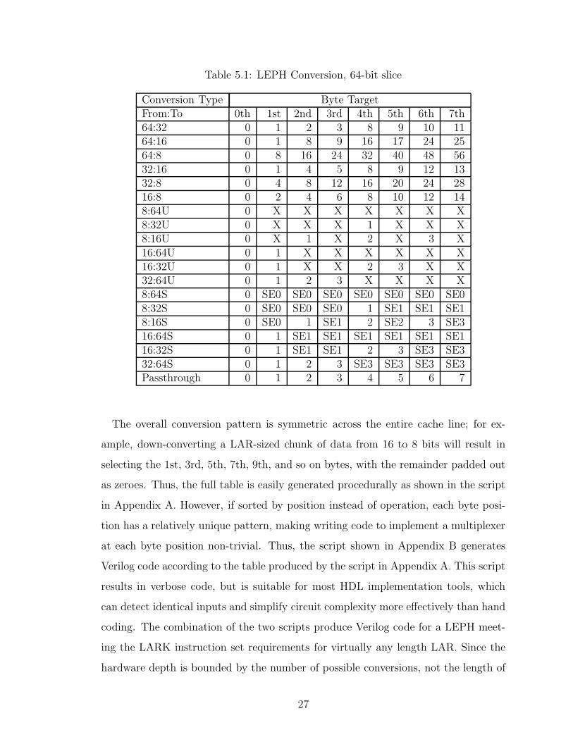
Table 5.1: LEPH Conversion, 64-bit slice
Conversion Type Byte TargetFrom:To 0th 1st 2nd 3rd 4th 5th 6th 7th64:32 0 1 2 3 8 9 10 1164:16 0 1 8 9 16 17 24 2564:8 0 8 16 24 32 40 48 5632:16 0 1 4 5 8 9 12 1332:8 0 4 8 12 16 20 24 2816:8 0 2 4 6 8 10 12 148:64U 0 X X X X X X X8:32U 0 X X X 1 X X X8:16U 0 X 1 X 2 X 3 X16:64U 0 1 X X X X X X16:32U 0 1 X X 2 3 X X32:64U 0 1 2 3 X X X X8:64S 0 SE0 SE0 SE0 SE0 SE0 SE0 SE08:32S 0 SE0 SE0 SE0 1 SE1 SE1 SE18:16S 0 SE0 1 SE1 2 SE2 3 SE316:64S 0 1 SE1 SE1 SE1 SE1 SE1 SE116:32S 0 1 SE1 SE1 2 3 SE3 SE332:64S 0 1 2 3 SE3 SE3 SE3 SE3Passthrough 0 1 2 3 4 5 6 7
The overall conversion pattern is symmetric across the entire cache line; for ex-
ample, down-converting a LAR-sized chunk of data from 16 to 8 bits will result in
selecting the 1st, 3rd, 5th, 7th, 9th, and so on bytes, with the remainder padded out
as zeroes. Thus, the full table is easily generated procedurally as shown in the script
in Appendix A. However, if sorted by position instead of operation, each byte posi-
tion has a relatively unique pattern, making writing code to implement a multiplexer
at each byte position non-trivial. Thus, the script shown in Appendix B generates
Verilog code according to the table produced by the script in Appendix A. This script
results in verbose code, but is suitable for most HDL implementation tools, which
can detect identical inputs and simplify circuit complexity more effectively than hand
coding. The combination of the two scripts produce Verilog code for a LEPH meet-
ing the LARK instruction set requirements for virtually any length LAR. Since the
hardware depth is bounded by the number of possible conversions, not the length of
27
the LAR, the hardware footprint should scale almost linearly.
5.4 Execution Hardware
Due to the type tagging present in LARs, the execution pipeline must be able to
detect and support operations on data of varying size. Such operations are supported
in a variety of ways in existing architectures. Often separate pipelines operate on
different sizes and types of data which incurs a penalty in overall hardware size. In
other architectures, configuring the existing pipeline to operate on a different type
requires a context switch, an approach commonly implemented for AVX. However, as
LOON is a demonstration architecture, it is desirable to keep hardware complexity to
a minimum while avoiding delays caused by context switches, which is not practical
under the LARK ISA where types may not even originally match.
Arithmetic Logical Unit (ALU)
Therefore, this architecture contains a carry-break Arithmetic Logic Unit, or a
carry-break ALU. To meet the requirements of LARK, this unit should be reconfig-
urable to operate on both signed and unsigned integers ranging in size from 8 bits
to 64 bits. It should be able to perform basic arithmetic and logic operations on all
supported integer data types.
Carry-break ALU
The carry-break ALU is distinguished from other ALUs by consisting of many
smaller ALUs, connected by a logic network that can continue or break carry prop-
agation based on data type and size. The length of the small internal ALUs is
determined by the smallest supported data type, in this case 8 bits. They are con-
nected in groups supporting the largest possible word, which is 64 bits under the
LARK instruction set, causing each group to contain eight ALUs. These ALUs are
connected by a set of seven multiplexers, which change the carry-in bit to each ALU
based on the operation type and data size. An example showing this multiplexer net-
28

work is shown in Figure 5.8. For example, if the ALU is operating on 32-bit signed
integers, the multiplexer between the ALU3 and ALU4 will break the carry chain,
causing ALUs 0-3 to operate on one 32-bit word while ALUs 4-7 operate on another
32-bit word.
29

� � � � � � � �
� � � � � � �
� � �
� � � �� � � �� � � �� � � �� � � �� � � �� � � � � � � � � � � �
" � # $ % & ' ( ) & *+
� � � � � � � �
" � , $ % & ' ( ) & *+
� � � � � � � �
" � # $ % & ' ( ) & * +
� � � � � � � �
" � - $ % & ' ( ) & * +
� � � � � � � �
" � # $ % & ' ( ) & *+
� � � � � � � �
" � , $ % & ' ( ) & * +
� � � � � � � �
" � # $ % & ' ( ) & *+
� � � � � � � �
. /
0 /
. 1
0 1
. 2
0 2
. 3
0 3
. 4
0 4
. 5
0 5
. 6
0 6
. 7
0 7
8 9 8 �8 � 8 � 8 � 8 � 8 � 8 :
� � � � � � � � � � � � � � � � � � � � � � � �
� � � � � � � �
� � � � � � � � � � � � � � � � � � � � � � � � � � � � � � � �
Figure 5.8: LOON Carry-break Arithmetic Logic Unit
30

Arithmetic Shift Unit (ASU)
Constructing a shift unit for a LARs based architecture presents a similar problem
to that of constructing an ALU. The simplest shifters shift only a single bit position at
a time, only operate on a single word length, and are eminently unsuited to operating
on data held in a LAR. More complex shifters are capable of arbitrary length shifts,
and some are capable of operating on a selection of word lengths.
Existing Examples in Cryptography
An example of such a shifter intended for general-purpose cryptography is found
in “Design and Implementation of Reconfigurable Shift Unit using FPGAs” by Yu
et al.[27] They designed an arbitrary-length shifter capable of operating on several
standard sized words from 4 bits up to 128 bits, used in cryptography schemes such
as DES and Twofish. To satisfy this end, they implemented multiple levels of shifters
performing shifts in powers-of-two increments, and enable signals on each level to
perform shifts of a length specified by a 5-bit input. For shorter-length words, the
top level shifters are disabled. For example, the shifters performing a shift of 32 bits
are unneeded if operating on 8 bit words.
Application to LARs
This design is also useful in a LARs based pipeline, as it requires no reconfiguration
for changes in word size. In the LOON architecture, the Arithmetic Shift Unit (ASU)
consists of six levels of shifters. These shifters perform shifts in powers of 2 incre-
ments ranging from 20 to 25, or 1 to 32 bits. Since the largest possible word in this
architecture is 64 bits, the shifter hardware consists of 32 identical sets, each capable
of operating on a single 64- bit word or multiple smaller words. Each set contains two
32-bit shifters, four 16-bit shifters, eight 8-bit shifters, sixteen 4-bit shifters, thirty-
two 2-bit shifters, and sixty-four 1-bit shifters. The bottom three levels of shifters
from 1 to 4 bits are always potentially active depending on the length of the shift,
while the upper levels should never be activated if they match or exceed the word
31

size.
Figure 5.9: LOON ASU 16-bit Multiplexer
Since the behavior of each shifter depends on both the word size and the type
of shift, the ASU is implemented as multiplexers, with each multiplexer choosing
from one of twelve inputs, one input for each possible combination of word size and
shift type. However, each input only consists of five potential cases: all zeroes, the
bits from the previous positions, the bits from the next positions, the top bit from
this position repeating for arithmetic right shifts, or pass bits for the same position
through to the next level. An example for the 16-bit multiplexer in the next-to-least
significant position is shown in Figure 5.9. The overall table of input types for each
multiplexer also displays high levels of symmetry, as shown in Table 5.2. Therefore,
a script parses this table and generates Verilog code for the ASU. While verbose, this
method provides broad amounts of information to the implementation tools, allowing
the tool to simplify the actual generated hardware to a higher degree than is possible
simplifying by hand.
Multiplication Unit
Constructing a multiplier unit suitable for the LARK instruction set faces similar
issues to the ALU. The unit must be capable of both scalar and vector operations, on
word sizes ranging from 8 to 64 bits. However, due to the fundamental nature of the
32

Table 5.2: Arithmetic Shift Unit Opcode Table
op/size 8 SLL 16 SLL 32 SLL 64 SLL 8 SRA 16 SRA 32 SRA 64 SRA 8 SRL 16 SRL 32 SRL 64 SRLopcode 0100 0101 0110 0111 1000 1001 1010 1011 1100 1101 1110 111132-0 0 0 0 1 3 3 3 3 0 0 0 032-1 0 0 0 0 3 3 3 2 0 0 0 216-0 0 0 1 1 3 3 3 3 0 0 0 016-1 0 0 0 1 3 3 2 2 0 0 2 216-2 0 0 1 1 3 3 3 2 0 0 0 216-3 0 0 0 0 3 3 2 2 0 0 2 28-0 0 1 1 1 3 3 3 3 0 0 0 08-1 0 0 1 1 3 2 2 2 0 2 2 28-2 0 1 1 1 3 3 2 2 0 0 2 28-3 0 0 0 1 3 2 2 2 0 2 2 28-4 0 1 1 1 3 3 3 2 0 0 0 28-5 0 0 1 1 3 2 2 2 0 2 2 28-6 0 1 1 1 3 3 2 2 0 0 2 28-7 0 0 0 0 3 2 2 2 0 2 2 24-0 1 1 1 1 3 3 3 3 0 0 0 04-1 0 1 1 1 2 2 2 2 2 2 2 24-2 1 1 1 1 3 2 2 2 0 2 2 24-3 0 0 1 1 2 2 2 2 2 2 2 24-4 1 1 1 1 3 3 2 2 0 0 2 24-5 0 1 1 1 2 2 2 2 2 2 2 24-6 1 1 1 1 3 2 2 2 0 2 2 24-7 0 0 0 1 2 2 2 2 2 2 2 24-8 1 1 1 1 3 3 3 2 0 0 0 24-9 0 1 1 1 2 2 2 2 2 2 2 24-10 1 1 1 1 3 2 2 2 0 2 2 24-11 0 0 1 1 2 2 2 2 2 2 2 24-12 1 1 1 1 3 3 2 2 0 0 2 24-13 0 1 1 1 2 2 2 2 2 2 2 24-14 1 1 1 1 3 2 2 2 0 2 2 24-15 0 0 0 0 2 2 2 2 2 2 2 22-0 1 1 1 1 3 3 3 3 0 0 0 02-1 1 1 1 1 2 2 2 2 2 2 2 22-2 1 1 1 1 2 2 2 2 2 2 2 22-3 0 1 1 1 2 2 2 2 2 2 2 22-4 1 1 1 1 3 2 2 2 0 2 2 22-5 1 1 1 1 2 2 2 2 2 2 2 22-6 1 1 1 1 2 2 2 2 2 2 2 22-7 0 0 1 1 2 2 2 2 2 2 2 22-8 1 1 1 1 3 3 2 2 0 0 2 22-9 1 1 1 1 2 2 2 2 2 2 2 22-10 1 1 1 1 2 2 2 2 2 2 2 22-11 0 1 1 1 2 2 2 2 2 2 2 22-12 1 1 1 1 3 2 2 2 0 2 2 22-13 1 1 1 1 2 2 2 2 2 2 2 22-14 1 1 1 1 2 2 2 2 2 2 2 22-15 0 0 0 1 2 2 2 2 2 2 2 22-16 1 1 1 1 3 3 3 2 0 0 0 22-17 1 1 1 1 2 2 2 2 2 2 2 22-18 1 1 1 1 2 2 2 2 2 2 2 22-19 0 1 1 1 2 2 2 2 2 2 2 22-20 1 1 1 1 3 2 2 2 0 2 2 22-21 1 1 1 1 2 2 2 2 2 2 2 22-22 1 1 1 1 2 2 2 2 2 2 2 22-23 0 0 1 1 2 2 2 2 2 2 2 22-24 1 1 1 1 3 3 2 2 0 0 2 22-25 1 1 1 1 2 2 2 2 2 2 2 22-26 1 1 1 1 2 2 2 2 2 2 2 22-27 0 1 1 1 2 2 2 2 2 2 2 22-28 1 1 1 1 3 2 2 2 0 2 2 22-29 1 1 1 1 2 2 2 2 2 2 2 22-30 1 1 1 1 2 2 2 2 2 2 2 22-31 0 0 0 0 2 2 2 2 2 2 2 2
33
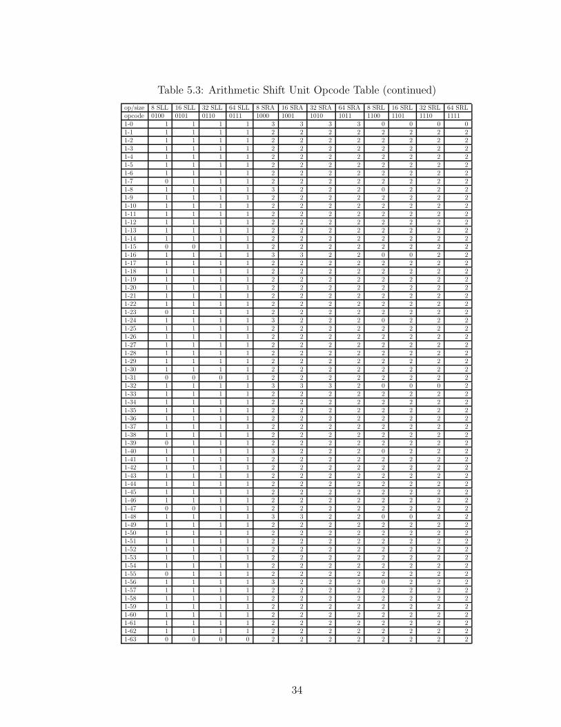
Table 5.3: Arithmetic Shift Unit Opcode Table (continued)
op/size 8 SLL 16 SLL 32 SLL 64 SLL 8 SRA 16 SRA 32 SRA 64 SRA 8 SRL 16 SRL 32 SRL 64 SRLopcode 0100 0101 0110 0111 1000 1001 1010 1011 1100 1101 1110 11111-0 1 1 1 1 3 3 3 3 0 0 0 01-1 1 1 1 1 2 2 2 2 2 2 2 21-2 1 1 1 1 2 2 2 2 2 2 2 21-3 1 1 1 1 2 2 2 2 2 2 2 21-4 1 1 1 1 2 2 2 2 2 2 2 21-5 1 1 1 1 2 2 2 2 2 2 2 21-6 1 1 1 1 2 2 2 2 2 2 2 21-7 0 1 1 1 2 2 2 2 2 2 2 21-8 1 1 1 1 3 2 2 2 0 2 2 21-9 1 1 1 1 2 2 2 2 2 2 2 21-10 1 1 1 1 2 2 2 2 2 2 2 21-11 1 1 1 1 2 2 2 2 2 2 2 21-12 1 1 1 1 2 2 2 2 2 2 2 21-13 1 1 1 1 2 2 2 2 2 2 2 21-14 1 1 1 1 2 2 2 2 2 2 2 21-15 0 0 1 1 2 2 2 2 2 2 2 21-16 1 1 1 1 3 3 2 2 0 0 2 21-17 1 1 1 1 2 2 2 2 2 2 2 21-18 1 1 1 1 2 2 2 2 2 2 2 21-19 1 1 1 1 2 2 2 2 2 2 2 21-20 1 1 1 1 2 2 2 2 2 2 2 21-21 1 1 1 1 2 2 2 2 2 2 2 21-22 1 1 1 1 2 2 2 2 2 2 2 21-23 0 1 1 1 2 2 2 2 2 2 2 21-24 1 1 1 1 3 2 2 2 0 2 2 21-25 1 1 1 1 2 2 2 2 2 2 2 21-26 1 1 1 1 2 2 2 2 2 2 2 21-27 1 1 1 1 2 2 2 2 2 2 2 21-28 1 1 1 1 2 2 2 2 2 2 2 21-29 1 1 1 1 2 2 2 2 2 2 2 21-30 1 1 1 1 2 2 2 2 2 2 2 21-31 0 0 0 1 2 2 2 2 2 2 2 21-32 1 1 1 1 3 3 3 2 0 0 0 21-33 1 1 1 1 2 2 2 2 2 2 2 21-34 1 1 1 1 2 2 2 2 2 2 2 21-35 1 1 1 1 2 2 2 2 2 2 2 21-36 1 1 1 1 2 2 2 2 2 2 2 21-37 1 1 1 1 2 2 2 2 2 2 2 21-38 1 1 1 1 2 2 2 2 2 2 2 21-39 0 1 1 1 2 2 2 2 2 2 2 21-40 1 1 1 1 3 2 2 2 0 2 2 21-41 1 1 1 1 2 2 2 2 2 2 2 21-42 1 1 1 1 2 2 2 2 2 2 2 21-43 1 1 1 1 2 2 2 2 2 2 2 21-44 1 1 1 1 2 2 2 2 2 2 2 21-45 1 1 1 1 2 2 2 2 2 2 2 21-46 1 1 1 1 2 2 2 2 2 2 2 21-47 0 0 1 1 2 2 2 2 2 2 2 21-48 1 1 1 1 3 3 2 2 0 0 2 21-49 1 1 1 1 2 2 2 2 2 2 2 21-50 1 1 1 1 2 2 2 2 2 2 2 21-51 1 1 1 1 2 2 2 2 2 2 2 21-52 1 1 1 1 2 2 2 2 2 2 2 21-53 1 1 1 1 2 2 2 2 2 2 2 21-54 1 1 1 1 2 2 2 2 2 2 2 21-55 0 1 1 1 2 2 2 2 2 2 2 21-56 1 1 1 1 3 2 2 2 0 2 2 21-57 1 1 1 1 2 2 2 2 2 2 2 21-58 1 1 1 1 2 2 2 2 2 2 2 21-59 1 1 1 1 2 2 2 2 2 2 2 21-60 1 1 1 1 2 2 2 2 2 2 2 21-61 1 1 1 1 2 2 2 2 2 2 2 21-62 1 1 1 1 2 2 2 2 2 2 2 21-63 0 0 0 0 2 2 2 2 2 2 2 2
34

multiply operation, scaling between different word sizes is significantly more difficult
than for addition. Although an add operation produces a n+1-bit result, given n-bit
operands, a multiply operation will produce a 2n-bit result. Thus, instead of simply
breaking the carry as for an add operation, a more sophisticated solution is required
in the multiply unit. Designers commonly implement a solution using increased radix
to increase multiply performance.[8][19][22]
Decomposition of Partial Products (DPP)
Examining the fundamental nature of the multiply operation, we find that for
a given radix, a multiply between operands of k-radix long may be expressed as
a sum of partial products. An example of multiplication for 4-radix long may be
found in Table 5.4. Further, if these operands are instead treated as two numbers
of 2-radix long, thus being two separate multiply operations, only a subset of the
partial products is required to calculate these two separate multiplies. Finally, if
the operands are instead treated as four separate numbers of a single radix long,
thus being four separate multiply operations, yet another subset of only one partial
product per multiply operation is required.
Table 5.4: Decomposition of Partial Products, 2 radix multiply highlighted
a b c d
X e f g h
d X h
c X h
b X h
a X h
d X g
c X g
b X g
a X g
d X f
c X f
b X f
a X f
d X e
c X e
b X e
a X e
1 radix: Not used 3rd result Not used 2nd result Not used 1st result Not used 0th result
2 radix: Not used 1st result Not used 0th result
4 radix: Not used 0th result
35

Implementation in Hardware
By taking advantage of this decomposition of partial products, a variable word size,
multiple clock cycle multiply unit can be constructed. Taking into consideration that
multiplies of shorter word sizes should take fewer cycles, the partial products should
be rearranged in such a way that as many partial products are added simultaneously
as possible, with priority given to the particular products required for shorter word
sizes. Building on our 4-radix long example, a version of such an arrangement is
provided in Table 5.5. The middle of the result requires more partial products due
to the nature of the multiply operation, so this arrangement takes the form of a
pyramid. These partial products are arranged in such a way that the number of
add cycles required to reach the result is 2k − 1, where k is the radix length of the
operands, i.e. 2 · 4− 1 = 7 cycles required for 4-radix long operands.
Table 5.5: DPP pyramid form. 2 radix multiply highlighted
a b c d
X e f g h
Clock Cycle
1 a X e b X f c X g d X h
2 a X f c X f c X h
3 b X e b X g d X g
4 a X g b X h
5 c X e d X f
6 d X e
7 a X h
1 radix: Not used 3rd result Not used 2nd result Not used 1st result Not used 0th result
2 radix: Not used 1st result Not used 0th result
4 radix: Not used 0th result
Expanding this design to the LARK specification, we require 64-bit, 32-bit, 16-bit,
and 8-bit operations. We can treat 8 bits as our radix by including 8×8 look up tables
in our base multiply unit. Thus, our potential lengths are 8 radix, 4 radix, 2 radix,
and 1 radix. A similar pyramid arrangement of the decomposed partial products for
8-radix-wide operands is found in Table 5.6. The maximum possible number of cycles
is 15 for the 64-bit operands, while finishing in a single cycle for 8-bit operands.
36

Table 5.6: DPP pyramid form for 8 radix. 4 radix multiply highlighted
a b c d e f g hX i j k l m n o p
Clock cycle1 i X a j X b k X c l X d m X e n X f o X g p X h2 j X a l X a l X c p X a n X e p X e p X g3 i X b k X b k X d o X b m X f o X f o X h4 k X a l X b o X a p X b p X d p X f5 I X c j X d n X b n X d o X e n X h6 j X c n X a n X c p X c n X g7 i X d m X b m X d o X d m X h8 m X a m X c o X c m X g9 i X e k X e l X f l X h10 j X e l X e l X g11 i X f k X f k X h12 j X f k X g13 i X g j X h14 j X g15 i X h
1 radix: Not used 7th result Not used 6th result Not used 5th result Not used 4th result Not used 3rd result Not used 2nd result Not used 1st result Not used 0th result2 radix: Not used 3rd result Not used 2nd result Not used 1st result Not used 0th result4 radix: Not used 1st result Not used 0th result8 radix: Not used 0th result
37

Converting this diagram to actual hardware, we find that eight 8 × 8 LUTs is
required for each 64-bit word slice. Since these LUTs are read-only, a significant
savings in hardware can be achieved by using a LUT with multiple read ports; using
a single 8 × 8 LUT with eight read ports is a feasible solution. Due to the single
byte offset of some levels of the two-byte partial products, a level of multiplexers is
required immediately after the LUTs to provide this offset. A 128-bit accumulator
is required to sum the partial products in each cycle. Finally, an array of eight byte
sized multiplexers is required to select the appropriate sections of the accumulator
result dependent on input word size.
Division Unit
Binary division tends to be a significantly more complicated problem than binary
multiplication, as shortcuts involving increased radix do not apply to division. Itera-
tive methods exist for division, but often destroy the remainder or cause undesirable
approximations.[21] However, unlike multiplication, integer division always produces
an n or less bit result given n-bit operands. Scaling between different word sizes is
therefore somewhat simpler than for multiplication.
Shift and Subtract Algorithm
LOON implements division by a “shift and subtract” algorithm, as shown in Table
5.7. Division is conducted by a series of steps: first, the dividend and divisor are
normalized to positive integers. Next, the divisor is shifted to the left such that its
highest bit is aligned with the highest bit of the dividend. Once alignment is complete,
the following two steps are repeated until the divisor returns to its original value:
the divisor and dividend are compared, and if the divisor is smaller, the dividend
is decremented by the divisor, and the quotient is set to 1 at the bit position of
the current divisor shift. Otherwise the quotient is set to zero. This step can be
streamlined by always performing the subtraction, and latching based on the sign of
the result. The divisor is then right shifted by one bit position, and the previous step
is repeated. Once these steps are complete, the positive quotient is fully described,
38
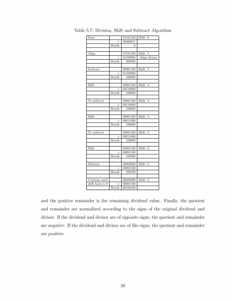
Table 5.7: Division, Shift and Subtract Algorithm
Start 01101100 Shift: 0÷ 00000011
Result 0
Align 01101100 Shift: 5÷ 01100000 Align divisor
Result 000000
Subtract 00001100 Shift: 5÷ 01100000
Result 100000
Shift 00001100 Shift: 4÷ 00110000
Result 100000
No subtract 00001100 Shift: 4÷ 00110000
Result 100000
Shift 00001100 Shift: 3÷ 00011000
Result 100000
No subtract 00001100 Shift: 3÷ 00011000
Result 100000
Shift 00001100 Shift: 2÷ 00001100
Result 100000
Subtract 00000000 Shift: 2÷ 00001100
Result 100100
Continue until 00000000 Shift: 2shift back to 0 ÷ 00001100
Result 00100100
and the positive remainder is the remaining dividend value. Finally, the quotient
and remainder are normalized according to the signs of the original dividend and
divisor. If the dividend and divisor are of opposite signs, the quotient and remainder
are negative. If the dividend and divisor are of like signs, the quotient and remainder
are positive.
39
; < = > ? @ A @ > B C >
D B E F < G H I J K L J M
M N F B L B = B E F ; O G > P O G B
; < = > ? @ A @ Q < G
D B E F < G H I J K L J M
M N F B L B = B E F ; O G > P O G B
R R
STUVWTXXYZY[\]
STUVWTXXYZY XTSX
^ G @ < G @ F N _ C E < > B G Q K ? B F B E F
; @ ` a B Q F M @ F Q
^ G @ < G @ F N _ C E < > B G Q K ? B F B E F
; @ ` a B Q F M @ F Qb c d e f g h i j k
k h l h m c db c d e f g h i j k
k h l h k j b k
n C A B G F B G Q
H > > B G
o p q r s t u v w
x p y t u z t u v w { p s
{ s s t u v q r p v x v z r |
r p t v t z | r u t { q }
~ r v v x � � t � r u s v x � t
H > > B G
�����
� � � Q B F ? @ � � B G B C E B Q K ? < P C
� < � C F J C @ F Q
I B � F H = @ ` C � B C F L a @ � F B G
� c d k � m h i j
; < = > H = @ ` C B > ? @ A @ Q < G
� @ ` a F L a @ � F B G
� � �
; < = > � � G G B C F ? @ A @ > B C >
� � �
D B E F < G H I J K L J M� � r z x t p z x v v t z { p s
� x y x s t p s x v � { z q } t s x |
p r z p t � { z x y t u t v � � z
� � < F @ B C F
D B E F < G H I J K L J M
M N F B L B = B E F ; O G > P O G B
R
� � c � h j b �� c � � d j e f h b k j d � c � �
k h l h k j b k � h b k h l h k m c d� h b
D B E F < G H I J K L J M
M N F B L B = B E F ; O G > P O G B
R
� � � � � � � � � � � � �� ¡ ¢ �
£ ¢ � ¢ ¤ � � � �
¥ ¦ � � §
¥ ¨ © � � � ¤ �
� � � � � � � � � � � � �
Figure 5.10: LOON Divider Unit
40
Implementation in Hardware
Implementing this algorithm in hardware in a manner capable of the word-size scal-
ing demanded by the LARK instruction set results in several interesting hardware
sections. First, the beginning normalization step requires another copy of the vector
ALU implemented for other arithmetic operations to perform negation on each word
of the specified size. The normalization steps also require hardware capable of detect-
ing the sign bits of the appropriate words and selecting the original or the negation
to get the positive value. Second, there must be hardware capable of detecting the
difference between the highest bit of the dividend and the highest bit of the divisor,
for each appropriate word size. This requirement results in fifteen pairs of priority
encoders, one in each pair for dividend and divisor and one pair per possible word
in each possible word size. There must also be a left shifter capable of acting with
differently sized shifts on every word in each word size. Finally, once the divisor and
dividend are aligned, the detected differences must count down, another vector ALU
must perform subtractions in the appropriate word sizes, and the quotients must be
set at the appropriate position based on the subtraction result and corresponding
detected difference. Finally, the ending normalization requires one additional vector
ALU and appropriate selection hardware as in the first step.
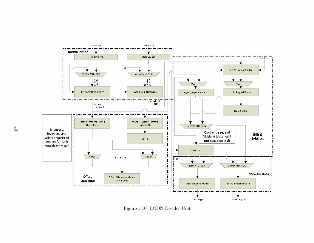
Figure 5.10 presents a diagram of the logical blocks found in the division unit.
This design results in a divider unit, capable of performing on n-bit operands in no
more than n + 4 steps, where operands may be 64-bit, 32-bit, 16-bit, or 8-bit signed
integers, suitable for the LARK instruction set architecture.
5.5 Writeback of Results
If the executed instruction was a vector operation, the Writeback stage is simple.
The result is simply sent back to the DLAR bank to be stored in the appropriate
DLAR. If instead the operation was a scalar operation, two operations must take
place: the scalar result must be shifted to the appropriate DLAR offset and the
41

result must be merged with the existing data in the DLAR. These operations take
place simultaneously within the WB Shifter, as the scalar result is simply latched
over the existing data in the DLAR at the provided offset. This new data line is then
sent to the DLAR bank.
Copyright c© Matthew Sparks, 2013.
42

Chapter 6 Problems with LARs
Due to their unconventional design, designing LARs into an architecture causes
problems with some solutions implemented in contemporary architectures. Input and
output to peripherals is difficult under the LARK ISA since there is no mechanism to
force data out to a memory address, and LARK does not contain other instructions
for input and output. Self-modifying code is also difficult to implement due to the
lack of a mechanism to force data to memory.
6.1 Input and Output
Input and output, or I/O, refers to communication between the processor/memory
system and any peripheral devices. I/O allows such necessities as keyboard and mouse
input to a computer, display of data to a video device, or sending information to a
printer. Two common methods of performing I/O are memory mapping, and port
mapping.
Memory-Mapped I/O
In memory-mapped I/O, addresses in memory space are assigned to correspond
with various peripherals and devices. To read or write data from a device, the pro-
cessor reads or writes to the appropriate memory location, effectively treating the
device as if it were memory. In traditional memory-cache systems, this method can
cause problems since the data at these “memory” addresses can change independent
of the processor. If the cache holds data belonging to a memory-mapped address, the
cached value will be provided upon read instead of the actual, potentially changed
value. This discrepancy can be resolved by specifying inside the program that the
value may change outside of the program’s control, such as by using C’s volatile key-
word. However, in LARs the cache-like behavior is far more integrated into the design
and cannot simply be bypassed. No mechanism exists for refreshing a DLAR from
43

memory if that memory location changes. “Lazy” writeback also presents problems
with writing to memory-mapped devices. Since there is no way in the LARK/LOON
design to definitively determine when a DLAR will be written back to memory, timing
and communication protocols become difficult if not impossible.
Port Mapped I/O
In port mapped I/O, a separate address space is defined for peripherals, and special
instructions are provided for reading and writing in this space. For example, in the x86
instruction set, the instructions IN and OUT provide these functions. This approach
would work reasonably well in a LAR-based architecture, as the I/O address space
is then separate from the caching behavior of the memory address space and is not
required to use LARs since their associative and caching behaviors are not required
in that context. However, the LARK instruction set architecture does not contain
instructions for port mapped I/O.
Conclusion
Overall, I/O presents a non-trivial problem in an entirely LAR-based architecture,
and falls outside the scope of the LOON architecture. Further iterations of the design
would likely include port-mapped I/O to clearly delineate between the LAR address
space and the peripheral address space.
6.2 Self-Modifying Code
Self-modifying code is a program that modifies its own instructions as it executes,
either through treating data like instructions, or through an explicit instruction for
modifying code. This concept presents an unusual issue in LARs due to the automatic
association between registers and memory. In particular, three problems arise: first,
since writeback of data to memory is “lazy”, there is no guarantee that modified
data is actually ready to be fetched as an instruction. Second, there is currently no
mechanism to refresh an ILAR if its corresponding memory location is changed. If
44

that memory location is already loaded into an ILAR, and is then modified elsewhere,
the modification will not reach the ILAR. Finally, although not implemented in the
LOON architecture, future development of LARs intends for compression on an ILAR
by ILAR basis in the instruction memory path in order to save bandwidth. Self-
modifying code would need to be aware of this compression scheme and be able
to appropriately package and compress an entire ILAR in order to accommodate.
Overall, LARs present many difficult challenges to self-modifying code which are not
covered by the scope of this work. In the LOON implementation, ILARs and the
corresponding memory locations are assumed to be read-only during the execution of
a program.
Copyright c© Matthew Sparks, 2013.
45

Chapter 7 Conclusions
7.1 Results
Virtually all of the sub-components of the LOON architecture are completed, and
basic functionality of each verified using Verilog testbenches running under Icarus
Verilog. We tested the multiplication unit, the divider unit, and the arithmetic shift
unit individually for multiple cases, including overflow, signed and unsigned arith-
metic, and all word sizes specified in the LARK ISA. We verified that the polymorphic
hardware units function for each possible conversion type. The entire memory system
including the ILAR and DLAR banks is assembled and tested for basic operations,
particularly LOAD, FETCH, and STORE instructions.
All Verilog modules, Verilog testbenches, and generation scripts in Perl and bash
are available online.[23]
7.2 Future Work
In conclusion, the LOON architecture is the most in-depth exploration of the con-
cept of Line Associative Registers to date. Its vector arithmetic units provide an
example of the incredible parallelism available through a LARs based architecture,
and its conversion units demonstrate capabilities that require pipeline flushes and
other delays in conventional architectures. An instruction that converts an entire
row of 256 bytes to 64 32-bit integers, performs 64 adds to another row of 32-bit
integers, and stores all results is not only viable but is normal within the LOON
architecture.
Future work with LARs-based architectures falls into several categories. Developing
a viable input/output scheme would help cement LARs as a usable architecture.
A more immediately promising approach would be integration of LAR-style type
46
and size tagging into existing SWAR instruction sets, such as AVX or SSE. These
formats already support the vector behavior of LARs, and integrating more LAR-
like characteristics would help bring some of the benefits of LARs into conventional
architectures. Finally, the instruction pipeline for a LARs-based architecture could
still benefit from an efficient instruction compression scheme, and would additionally
mitigate the effect of the memory gap.
Copyright c© Matthew Sparks, 2013.
47

Appendix A LEPH Table Generation
#!/bin/bashe ho -n "Line size: "read lineSize ;let i=1;let k=0;while [ $k -lt $lineSize ]doif(($i < $lineSize )); thenprintf "$i ,";let i=$i+1;
printf "$i ,";let i=$i+1;
printf "$i ,";let i=$i+1;
printf "$i ,";let i=$i+5;let k=k+4;elseprintf "0,";let k=k+1;fidone
printf ’\n’;let i=1;let k=0;while [ $k -lt $lineSize ]doif(($i < $lineSize )); thenprintf "$i ,";let i=$i+1;
printf "$i ,";let i=$i+7;let k=k+2;elseprintf "0,";let k=k+1;
48
fidoneprintf ’\n’;let i=1;let k=0;while [ $k -lt $lineSize ]doif(($i < $lineSize )); then
printf "$i ,";let i=$i+8;let k=k+1;elseprintf "0,";let k=k+1;fidone
printf ’\n’;let i=1;let k=0;while [ $k -lt $lineSize ]doif(($i < $lineSize )); thenprintf "$i ,";let i=$i+1;
printf "$i ,";let i=$i+3;let k=k+2;elseprintf "0,";let k=k+1;fidone
printf ’\n’;let i=1;let k=0;while [ $k -lt $lineSize ]doif(($i < $lineSize )); thenprintf "$i ,";
49

let i=$i+4;let k=k+1;elseprintf "0,";let k=k+1;fidone
printf ’\n’;let i=1;let k=0;while [ $k -lt $lineSize ]doif(($i < $lineSize )); thenprintf "$i ,";let i=$i+2;let k=k+1;elseprintf "0,";let k=k+1;fidone
printf ’\n’;let i=1;let k=0;while [ $k -lt $lineSize ]doif(($i < $lineSize )); thenprintf "$i ,";let i=$i+1;
printf "0,0,0,0,0,0,0,";let k=k+8;elseprintf "0,";let k=k+1;fidone
printf ’\n’;let i=1;let k=0;
50

while [ $k -lt $lineSize ]doif(($i < $lineSize )); thenprintf "$i ,";let i=$i+1;
printf "0,0,0,";let k=k+4;elseprintf "0,";let k=k+1;fidone
printf ’\n’;let i=1;let k=0;while [ $k -lt $lineSize ]doif(($i < $lineSize )); thenprintf "$i ,";let i=$i+1;
printf "0,";let k=k+2;elseprintf "0,";let k=k+1;fidone
printf ’\n’;let i=1;let k=0;while [ $k -lt $lineSize ]doif(($i < $lineSize )); thenprintf "$i ,";let i=$i+1;
printf "$i ,";let i=$i+1;
printf "0,0,0,0,0,0, ";let k=k+8;elseprintf "0,";
51
let k=k+1;fidoneprintf ’\n’;let i=1;let k=0;while [ $k -lt $lineSize ]doif(($i < $lineSize )); then
printf "$i ,";let i=$i+1;
printf "$i ,";let i=$i+1;
printf "0,0,";let k=k+4;elseprintf "0,";let k=k+1;fidone
printf ’\n’;let i=1;let k=0;while [ $k -lt $lineSize ]doif(($i < $lineSize )); thenprintf "$i ,";let i=$i+1;
printf "$i ,";let i=$i+1;
printf "$i ,";let i=$i+1;
printf "$i ,";let i=$i+1;
printf "0,0,0,0,";let k=k+8;elseprintf "0,";let k=k+1;fidone
52
printf ’\n’;let i=1;let k=0;while [ $k -lt $lineSize ]doif(($i < $lineSize )); thenprintf "$i ,";e ho -n "-$i ,-$i ,-$i ,-$i ,-$i ,-$i ,-$i ,";let i=$i+1;let k=k+8;elseprintf "0,";let k=k+1;fidone
printf ’\n’;let i=1;let k=0;while [ $k -lt $lineSize ]doif(($i < $lineSize )); thenprintf "$i ,";e ho -n "-$i ,-$i ,-$i ,";let i=$i+1;let k=k+4;elseprintf "0,";let k=k+1;fidone
printf ’\n’;let i=1;let k=0;while [ $k -lt $lineSize ]doif(($i < $lineSize )); thenprintf "$i ,";e ho -n "-$i ,";let i=$i+1;
53
let k=k+2;elseprintf "0,";let k=k+1;fidone
printf ’\n’;let i=1;let k=0;while [ $k -lt $lineSize ]doif(($i < $lineSize )); thenprintf "$i ,";let i=$i+1;
printf "$i ,";e ho -n "-$i ,-$i ,-$i ,-$i ,-$i ,-$i ,";let i=$i+1;let k=k+8;elseprintf "0,";let k=k+1;fidone
printf ’\n’;let i=1;let k=0;while [ $k -lt $lineSize ]doif(($i < $lineSize )); thenprintf "$i ,";let i=$i+1;
printf "$i ,";e ho -n "-$i ,-$i ,";let i=$i+1;let k=k+4;elseprintf "0,";let k=k+1;fidone
54
printf ’\n’;let i=1;let k=0;while [ $k -lt $lineSize ]doif(($i < $lineSize )); thenprintf "$i ,";let i=$i+1;
printf "$i ,";let i=$i+1;
printf "$i ,";let i=$i+1;
printf "$i ,";e ho -n "-$i ,-$i ,-$i ,-$i ,";let i=$i+1;let k=k+8;elseprintf "0,";let k=k+1;fidone
printf ’\n’;let i=1;let k=0;while [ $k -lt $lineSize ]doprintf "$i ,";let i=$i+1;let k=k+1;done
printf ’\n’;
55
Appendix B LEPH Code Generation from Table
#!/usr/bin/perluse strict;use warnings ;my $file = $ARGV [0] or die "No CSV file given.\n";open(my $data , ’<’, $file) or die "Could not open ’$file’
$!\n";my $byteNum = 0;while (my $line = <$data >)
{ print "byteSelector bs".$byteNum ."(out[".( $byteNum
*8+7).":".( $byteNum *8)."],";print "{"; homp $line;my @fields = split "," , $line;my $thisField ;my $firstFlag = 0;forea h $thisField (@fields )
{ if($firstFlag == 0)
{
$firstFlag = 1;
}else{ print ",";
}if($thisField == 0)
{ print "8’b00000000 ";
}elsif($thisField > 0)
{
$thisField --;print "in[";
56

print ($thisField *8+7);print ":";print ($thisField *8);print "]";
}elsif($thisField < 0)
{
$thisField = abs($thisField ) - 1;print "{";print "in[";print ($thisField *8+7);print "]";my $count;for($count = 0; $count < 7; $count
++)
{ print ",";print "in[";print ($thisField *8+7);print "]";
}print "}";
}else{ print $thisField ;
}
}
$byteNum ++;print "}";print ",op_type );\n";
}
57

Bibliography
[1] John Randal Allen. “Dependence analysis for subscripted variables and itsapplication to program transformations”. AAI8314916. PhD thesis. Houston,TX, USA, 1983.
[2] Tom Blank. “The maspar mp-1 architecture”. In: IEEE Compcon. 1990,pp. 20–24.
[3] C.-H. Chi and H. Dietz. “Unified management of registers and cache usingliveness and cache bypass”. In: SIGPLAN Not. 24.7 (June 1989), pp. 344–353.issn: 0362-1340. doi: 10.1145/74818.74849. url: http://doi.acm.org/10.1145/74818.74849.
[4] Robert P. Colwell et al. “A VLIW architecture for a trace schedulingcompiler”. In: IEEE Transactions on Computers 37.8 (Aug. 1988),pp. 967–979.
[5] Peter Dahl and Matthew O’Keefe. “Reducing Memory Traffic with CRegs”.In: Proceedings of the 27th Annual Symposium on Microarchitecture.Association for Computing Machinery. 1994.
[6] H. Dietz and C. H. Chi. “CRegs: a new kind of memory for referencing arraysand pointers”. In: Proceedings of the 1988 ACM/IEEE conference onSupercomputing. Supercomputing ’88. Los Alamitos, CA, USA: IEEEComputer Society Press, 1988, pp. 360–367. isbn: 0-8186-0882-X. url:http://dl.acm.org/citation.cfm?id=62972.63018.
[7] Paul S. Eberhart and Henry G. Dietz. A Compiler Target Model for LineAssociative Registers. 2010. url: http://aggregate.org/LAR/larscpc10.pdf.
[8] M.D. Ercegovac and T. Lang. “Fast multiplication without carry-propagateaddition”. In: Computers, IEEE Transactions on 39.11 (1990), pp. 1385–1390.issn: 0018-9340. doi: 10.1109/12.61047.
[9] Randall James Fisher. “General-purpose simd within a register: parallelprocessing on consumer microprocessors”.http://aggregate.org/LAR/fisher.pdf. PhD thesis. Purdue University, 2003.
[10] John Hennessy et al. “MIPS: A microprocessor architecture”. In: SIGMICRONewsl. 13.4 (Oct. 1982), pp. 17–22. issn: 1050-916X. url: http://dl.acm.org/citation.cfm?id=1014194.800930.
[11] John L. Hennessy and David A. Patterson. Computer Architecture: AQuantitative Approach. 5th ed. San Francisco, CA, USA: Morgan KaufmannPublishers Inc., 2011. isbn: 012383872X.
[12] Rajeev Kumar and Anil Vohra. “Design of Variable Width Barrel Shifter forHigh Speed Processor Architecture”. In: International Journal of EngineeringScience and Technology 4.4 (2012), pp. 1728–1733.
58
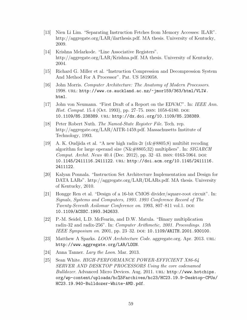
[13] Nien Li Lim. “Separating Instruction Fetches from Memory Accesses: ILAR”.http://aggregate.org/LAR/ilarthesis.pdf. MA thesis. University of Kentucky,2009.
[14] Krishna Melarkode. “Line Associative Registers”.http://aggregate.org/LAR/Krishna.pdf. MA thesis. University of Kentucky,2004.
[15] Richard G. Miller et al. “Instruction Compression and Decompression SystemAnd Method For A Processor”. Pat. US 5819058.
[16] John Morris. Computer Architecture: The Anatomy of Modern Processors.1998. url: http://www.cs.auckland.ac.nz/~jmor159/363/html/VLIW.html.
[17] John von Neumann. “First Draft of a Report on the EDVAC”. In: IEEE Ann.Hist. Comput. 15.4 (Oct. 1993), pp. 27–75. issn: 1058-6180. doi:10.1109/85.238389. url: http://dx.doi.org/10.1109/85.238389.
[18] Peter Robert Nuth. The Named-State Register File. Tech. rep.http://aggregate.org/LAR/AITR-1459.pdf. Massachusetts Institute ofTechnology, 1993.
[19] A. K. Oudjida et al. “A new high radix-2r (r≥8) multibit recodingalgorithm for large operand size (N≥32) multipliers”. In: SIGARCHComput. Archit. News 40.4 (Dec. 2012), pp. 32–43. issn: 0163-5964. doi:10.1145/2411116.2411122. url: http://doi.acm.org/10.1145/2411116.2411122.
[20] Kalyan Ponnala. “Instruction Set Architecture Implementation and Design forDATA LARs”. http://aggregate.org/LAR/DLARs.pdf. MA thesis. Universityof Kentucky, 2010.
[21] Hongge Ren et al. “Design of a 16-bit CMOS divider/square-root circuit”. In:Signals, Systems and Computers, 1993. 1993 Conference Record of TheTwenty-Seventh Asilomar Conference on. 1993, 807–811 vol.1. doi:10.1109/ACSSC.1993.342633.
[22] P.-M. Seidel, L.D. McFearin, and D.W. Matula. “Binary multiplicationradix-32 and radix-256”. In: Computer Arithmetic, 2001. Proceedings. 15thIEEE Symposium on. 2001, pp. 23–32. doi: 10.1109/ARITH.2001.930100.
[23] Matthew A Sparks. LOON Architecture Code. aggregate.org. Apr. 2013. url:http://www.aggregate.org/LAR/LOON.
[24] Anna Tanner. Lary the Loon. Mar. 2013.
[25] Sean White. HIGH-PERFORMANCE POWER-EFFICIENT X86-64SERVER AND DESKTOP PROCESSORS Using the core codenamedBulldozer. Advanced Micro Devices. Aug. 2011. url: http://www.hotchips.org/wp-content/uploads/hc%5Farchives/hc23/HC23.19.9-Desktop-CPUs/
HC23.19.940-Bulldozer-White-AMD.pdf.
59

[26] Maurice V. Wilkes. “The Memory Gap and the Future of High PerformanceMemories”. In: ACM SIGARCH Computer Architecture News 29.1 (Mar.2001), pp. 2–7.
[27] Xuerong Yu et al. “Design and Implementation of Reconfigurable Shift Unitusing FPGAs”. In: Pervasive Computing and Applications, 2006 1stInternational Symposium on. 2006, pp. 543–545. doi:10.1109/SPCA.2006.297479.
60

Vita
Education
• University of Kentucky - Bachelor of Science in Computer Engineering, GPA 3.97
Professional Experience
• Lexmark International, Inc - Firmware Engineer Intern, May 2012 to August 2012
• North American Stainless - Engineering Intern, May 2011 to August 2011
• US Army Aberdeen Test Center, Army Test and Evaluation Command - EngineeringIntern, May 2010 to August 2010
Scholastic Honors
• Northern Kentucky/Greater Cincinnati UK Alumni Club Fellowship, Fall 2012
• Lexmark Fellowship, Fall 2011 - Spring 2012
• University Scholar Program at University of Kentucky
• Dean’s List, all undergraduate semesters
• National Merit Scholar
61